ONET1130EC 11.7 Gbps Transceiver with Dual CDRs and ... · PDF file1• Dual CDR with...
63
VCC_TX TXIN+ TXIN- TX_LF GND RXIN+ SDA RX_LF VCC_RX RXOUT+ VCC_RX RX_LOS RXIN- GND SCK GND LOL GND PD RXOUT- VDD VCC_TX TXOUT+ TXOUT- ONET1130EC TXIN+ TXIN- 0.1F 0.1F LOL TX_DIS 0.1F Laser VCC_TX 0.1F 0.1F Modulator Anode EA BIAS 50 PD EML TOSA 0.1F RXIN+ RXIN- 0.1F SDA SCK BIAS 0.1F VCC_RX RXOUT- RXOUT+ 0.1F 0.1F MONP 0.1F 0.1F PD 2.2nF 2.2nF MONB MONP AMP COMP TX_DIS TX_FLT RX_DIS MONB TX_FLT VDD LOS 0.01F 0.1F PD 4.7k to10k VCC_R 4.7k to10k VCC_T 4.7k to10k VCC 4.7k to10k VCC 4.7k to10k 4.7k to10k Product Folder Sample & Buy Technical Documents Tools & Software Support & Community ONET1130EC SLLSEJ3A – JUNE 2015 – REVISED JULY 2015 ONET1130EC 11.7 Gbps Transceiver with Dual CDRs and Modulator Driver The transmit path consists of an adjustable input 1 Features equalizer for equalization of up to 300 mm 1• Dual CDR with 9.80-11.7 Gbps Reference-Free (12 inches) of microstrip or stripline transmission line Operation of FR4 printed circuit boards, a multi-rate CDR and • 2-Wire Digital Interface with Integrated DACs and an output modulator driver. Output waveform control, in the form of cross-point adjustment and de- ADC for Control and Diagnostic Management emphasis are available to improve the optical eye • Output Polarity Select for TX and RX mask margin. Bias current for the laser is provided • Programmable Jitter Transfer Bandwidth and an integrated automatic power control (APC) loop • Electrical and Optical Loopback. to compensate for variations in average optical power over voltage, temperature and time is included. • CDR Bypass Mode for Low Data Rate Operation • Integrated Modulator Driver with Output Amplitude The receive path consists of a limiting amplifier with programmable equalization and threshold adjustment, up to 2 V PP Single-ended and Bias Current up to a multi-rate CDR and output de-emphasis to 150 mA Source. compensate for frequency dependent loss of • Automatic Power Control (APC) Loop with connectors, microstrips or striplines connected to the Selectable Monitor PD Range output of the device, The receiver output amplitude • Programmable TX Input Equalizer and loss of signal assert level can be adjusted. • TX Cross-Point Adjust and De-Emphasis Device Information • Includes Laser Safety Features ORDER NUMBER PACKAGE (PIN) BODY SIZE • Integrated Limiting Amplifier with Programmable ONET1130EC VQFN (32) 4.00 mm x 4.00 mm LOS Threshold • Adjustable RX Equalization and Input Threshold Simplified Schematic • Programmable RX Output Voltage and De- emphasis. • Power Supply Monitor and Temperature Sensor • Single 2.5-V Supply • –40°C to 100°C Operation • Surface Mount 4 mm x 4 mm 32-Pin QFN Package with 0.4 mm Pitch 2 Applications • XFP and SFP+ 10 Gbps SONET OC-192 Optical Transceivers • XFP and SFP+ 10 GBASE-ER/ZR Optical Transceivers 3 Description The ONET1130EC is a 2.5 V integrated modulator driver and limiting amplifier with transmit and receive clock and data recovery (CDR) designed to operate between 9.80 Gbps and 11.7 Gbps without the need for a reference clock. Optical and electrical loopback are included. CDR bypass mode can be used for operation at lower data rates and a two-wire serial interface allows digital control of the features. 1 An IMPORTANT NOTICE at the end of this data sheet addresses availability, warranty, changes, use in safety-critical applications, intellectual property matters and other important disclaimers. PRODUCTION DATA.
Transcript of ONET1130EC 11.7 Gbps Transceiver with Dual CDRs and ... · PDF file1• Dual CDR with...

VC
C_T
X
TXIN+
TXIN-
TX
_LF
GND
RXIN+
SDA
RX
_LF
VC
C_R
X
RX
OU
T+
VC
C_R
X
RX_LOS
RXIN-
GND
SCK
GND
LOL
GND
PD
RX
OU
T-
VD
D
VC
C_T
X
TX
OU
T+
TX
OU
T-
ONET1130ECTXIN+
TXIN-
0.1�F
0.1�F
LOL
TX_DIS
0.1�F
Laser
VCC_TX
0.1�F 0.1�F
Modulator Anode
EA BIAS
50
PD
EML TOSA
0.1�F
RXIN+
RXIN-
0.1�F
SDA
SCK
BIA
S
0.1�F
VCC_RX
RXOUT-
RXOUT+
0.1�F
0.1�F
MONP
0.1�F 0.1�F
PD
2.2nF
2.2nF
MONB
MONP
AM
P
COMP
TX
_DIS
TX
_FLT
RX
_DIS
MONB
TX_FLT
VDD
LOS0.01�F
0.1�F
PD
4.7k to10k
VCC_R
4.7k to10k
VCC_T
4.7k to10k
VCC
4.7k to10k
VCC
4.7k to10k
4.7k to10k
Product
Folder
Sample &Buy
Technical
Documents
Tools &
Software
Support &Community
ONET1130ECSLLSEJ3A –JUNE 2015–REVISED JULY 2015
ONET1130EC 11.7 Gbps Transceiver with Dual CDRs and Modulator DriverThe transmit path consists of an adjustable input1 Featuresequalizer for equalization of up to 300 mm
1• Dual CDR with 9.80-11.7 Gbps Reference-Free (12 inches) of microstrip or stripline transmission lineOperation of FR4 printed circuit boards, a multi-rate CDR and
• 2-Wire Digital Interface with Integrated DACs and an output modulator driver. Output waveform control,in the form of cross-point adjustment and de-ADC for Control and Diagnostic Managementemphasis are available to improve the optical eye• Output Polarity Select for TX and RXmask margin. Bias current for the laser is provided
• Programmable Jitter Transfer Bandwidth and an integrated automatic power control (APC) loop• Electrical and Optical Loopback. to compensate for variations in average optical power
over voltage, temperature and time is included.• CDR Bypass Mode for Low Data Rate Operation• Integrated Modulator Driver with Output Amplitude The receive path consists of a limiting amplifier with
programmable equalization and threshold adjustment,up to 2 VPP Single-ended and Bias Current up toa multi-rate CDR and output de-emphasis to150 mA Source.compensate for frequency dependent loss of• Automatic Power Control (APC) Loop with connectors, microstrips or striplines connected to theSelectable Monitor PD Range output of the device, The receiver output amplitude
• Programmable TX Input Equalizer and loss of signal assert level can be adjusted.• TX Cross-Point Adjust and De-Emphasis
Device Information• Includes Laser Safety FeaturesORDER NUMBER PACKAGE (PIN) BODY SIZE• Integrated Limiting Amplifier with Programmable
ONET1130EC VQFN (32) 4.00 mm x 4.00 mmLOS Threshold• Adjustable RX Equalization and Input Threshold
Simplified Schematic• Programmable RX Output Voltage and De-
emphasis.• Power Supply Monitor and Temperature Sensor• Single 2.5-V Supply• –40°C to 100°C Operation• Surface Mount 4 mm x 4 mm 32-Pin QFN
Package with 0.4 mm Pitch
2 Applications• XFP and SFP+ 10 Gbps SONET OC-192 Optical
Transceivers• XFP and SFP+ 10 GBASE-ER/ZR Optical
Transceivers
3 DescriptionThe ONET1130EC is a 2.5 V integrated modulatordriver and limiting amplifier with transmit and receiveclock and data recovery (CDR) designed to operatebetween 9.80 Gbps and 11.7 Gbps without the needfor a reference clock. Optical and electrical loopbackare included. CDR bypass mode can be used foroperation at lower data rates and a two-wire serialinterface allows digital control of the features.
1
An IMPORTANT NOTICE at the end of this data sheet addresses availability, warranty, changes, use in safety-critical applications,intellectual property matters and other important disclaimers. PRODUCTION DATA.

ONET1130ECSLLSEJ3A –JUNE 2015–REVISED JULY 2015 www.ti.com
Table of Contents8.2 Functional Block Diagram ....................................... 201 Features .................................................................. 18.3 Feature Description................................................. 212 Applications ........................................................... 18.4 Device Functional Modes........................................ 313 Description ............................................................. 18.5 Programming .......................................................... 314 Revision History..................................................... 28.6 Register Mapping .................................................... 325 Description (continued)......................................... 3
9 Application Information and Implementations . 496 Pin Configuration and Function ........................... 39.1 Application Information............................................ 497 Specifications......................................................... 5 9.2 Typical Application, Transmitter Differential Mode.. 49
7.1 Absolute Maximum Ratings ..................................... 5 10 Power Supply Recommendations ..................... 537.2 ESD Ratings ............................................................ 511 Layout................................................................... 547.3 Recommended Operating Conditions....................... 5
11.1 Layout Guidelines ................................................. 547.4 Thermal Information .................................................. 611.2 Layout Example .................................................... 547.5 DC Electrical Characteristics .................................... 6
12 Device and Documentation Support ................. 557.6 Transmitter AC Electrical Characteristics ................. 812.1 Community Resources.......................................... 557.7 Receiver AC Electrical Characteristics ..................... 912.2 Trademarks ........................................................... 557.8 Timing Requirements .............................................. 1012.3 Electrostatic Discharge Caution............................ 557.9 Typical Characteristics ............................................ 1312.4 Glossary ................................................................ 558 Detailed Description ............................................ 19
13 Mechanical, Packaging, and Orderable8.1 Overview ................................................................. 19Information ........................................................... 55
4 Revision HistoryNOTE: Page numbers for previous revisions may differ from page numbers in the current version.
Changes from Original (June 2015) to Revision A Page
• Changed From: Product Preview To Production ................................................................................................................... 1
2 Submit Documentation Feedback Copyright © 2015, Texas Instruments Incorporated
Product Folder Links: ONET1130EC

1
3
2
4
9 1110 12
21
22
23
24
29303132 25262728
5
7
6
8 17
18
19
20
13 1514 16
TX
_DIS
RX
OU
T+
RX
OU
T±
TX
_FLT
VC
C_R
X
VC
C_R
X
RX
_LF
RX
_DIS
MONB
LOL
TXIN±
TXIN+
GND
PD
MONP
GND
BIA
S
TX
_LF
VC
C_T
X
TX
OU
T+
TX
OU
T±
VC
C_T
X
VD
D
AM
P
RXIN±
RXIN+
RX_LOS
GND
GND
SDA
SCK
COMP
EP
ONET1130ECwww.ti.com SLLSEJ3A –JUNE 2015–REVISED JULY 2015
5 Description (continued)The ONET1130EC contains internal analog to digital and digital to analog converters to support transceivermanagement and eliminate the need for special purpose microcontrollers.
The transceiver is characterized for operation from –40°C to 100°C case temperatures and is available in a smallfootprint 4mm × 4mm, 32 pin RoHS compliant VQFN package.
6 Pin Configuration and Function
RSM PACKAGE32 PIN VQFN(TOP VIEW)
Pin FunctionsNUMBER NAME Type DESCRIPTION
Output amplitude control. Output amplitude can be adjusted by applying a voltage ofAMP 16 Analog-in 0 to 2 V to this pin. Leave open when not used.BIAS 10 Analog Sinks or sources the bias current for the laser in both APC and open loop modes.
Compensation pin used to control the bandwidth of the APC loop. Connect a 0.01-µFCOMP 23 Analog capacitor to ground.GND 3, 6, 19, 22 Supply Circuit ground.
Transmitter and receiver loss of lock indicator. High level indicates the transmitter orLOL 1 Digital-out the receiver is out of lock. Open drain output. Requires an external 4.7 kΩ to 10 kΩ
pull-up resistor to VCC for proper operation. This pin is 3.3 V tolerant.MONB 2 Analog-out Bias current monitor.MONP 8 Analog-out Photodiode current monitor.PD 7 Analog Photodiode input. Pin can source or sink current dependent on register setting.
Disables the receiver output buffer when set to a high level. Includes a 250-kΩ pull-RX_DIS 26 Digital-in up resistor to VCC. Ground the pin to enable the output. This is an ORed function
with the RXOUT_DIS bit (bit 6 in register 4). This pin is 3.3-V tolerant.RX_LF 25 Analog-in Receiver loop filter capacitor.
Receiver loss of signal. High level indicates that the receiver input signal amplitude isRX_LOS 24 Digital-out below the programmed threshold level. Open drain output. Requires an external 4.7-
kΩ to 10-kΩ pull-up resistor to VCC for proper operation. This pin is 3.3-V tolerant.Non-inverted receiver data input. On-chip differentially 100 Ω terminated to RXIN–.RXIN+ 20 Analog-in Must be AC coupled.Inverted receiver data input. On-chip differentially 100 Ω terminated to RXIN+. MustRXIN- 21 Analog-in be AC coupled.
RXOUT– 28 CML-out Inverted receiver data output. 45 Ω back-terminated to VCC.RXOUT+ 29 CML-out Non-inverted data output. 45 Ω back-terminated to VCC.
Copyright © 2015, Texas Instruments Incorporated Submit Documentation Feedback 3
Product Folder Links: ONET1130EC
ONET1130ECSLLSEJ3A –JUNE 2015–REVISED JULY 2015 www.ti.com
Pin Functions (continued)NUMBER NAME Type DESCRIPTION
2-wire interface serial data input. Requires an external 4.7-kΩ to10-kΩ pull-up resistorSDA 17 Digital-in/out to VCC. This pin is 3.3-V tolerant.2-wire interface serial clock input. Requires an external 4.7-kΩ to10-kΩ pull-upSCK 18 Digital-in resistor to VCC. This pin is 3.3-V tolerant.Disables both bias and modulation currents when set to high state. Includes a 250-kΩpull-up resistor to VCC. Requires an external 4.7 kΩ to 10 kΩ pull-up resistor to VCCTX_DIS 32 Digital-in for proper operation Toggle to reset a fault condition. This is an ORed function withthe TXBIASEN bit (bit 2 in register 1). This pin is 3.3-V tolerant.Non-inverted transmitter data input. On-chip differentially 100 Ω terminated to TXIN–.TXIN+ 4 Analog-in Must be AC coupled.Inverted transmitter data input. On-chip differentially 100 Ω terminated to TXIN+. MustTXIN– 5 Analog-in be AC coupled.
TX_LF 9 Analog-in Transmitter loop filter capacitor.Transmitter fault detection flag. High level indicates that a fault has occurred. Open
TX_FLT 31 Digital-out drain output. Requires an external 4.7 kΩ to 10 kΩ pull-up resistor to VCC for properoperation. This pin is 3.3-V tolerant.Inverted transmitter data output. Internally terminated in single-ended operationTXOUT– 12 CML-out mode.
TXOUT+ 13 CML-out Non-Inverted transmitter data output.VCC_RX 27, 30 Supply 2.5 V ± 5% supply for the receiver.VCC_TX 11, 14 Supply 2.5 V ± 5% supply for the transmitter.VDD 15 Supply 2.5 V ± 5% supply for the digital circuitry.Exposed Pad EP Exposed die pad. Solder to the PCB.
4 Submit Documentation Feedback Copyright © 2015, Texas Instruments Incorporated
Product Folder Links: ONET1130EC
ONET1130ECwww.ti.com SLLSEJ3A –JUNE 2015–REVISED JULY 2015
7 Specifications
7.1 Absolute Maximum Ratings (1) (2)
over operating free-air temperature range (unless otherwise noted)MIN MAX UNIT
Supply voltage at VCC_TX, VCC_RX, VDD –0.5 3 Vat 3.3-V tolerant pins LOL, SDA, SCK, RX_LOS, RX_DIS, V–0.5 3.6TX_FLT, TX_DIS
Voltage at all other pins MONB, TXIN+, TXIN–, PD, MONP, TX_LF,BIAS, TXOUT–, TXOUT+, AMP, RXIN+, RXIN–, COMP, –0.5 3 VRX_LF, RXOUT–, RXOUT+,
Maximum current at transmitter input pins TXIN+, TXIN– 10 mAMaximum current at transmitter output TXOUT+, TXOUT– 125 mApinsMaximum current at receiver input pins RXIN+, RXIN– 10 mAMaximum current at receiver output pins RXOUT+, RXOUT– 30 mAMaximum junction temperature, TJ 125 °CStorage temperature, Tstg –65 150 °C
(1) Stresses beyond those listed under “absolute maximum ratings” may cause permanent damage to the device. These are stress ratingsonly and functional operation of the device at these or any other conditions beyond those indicated under “recommended operatingconditions” is not implied. Exposure to absolute–maximum–rated conditions for extended periods may affect device reliability.
(2) All voltage values are with respect to network ground terminal.
7.2 ESD RatingsVALUE UNIT
Human-body model (HBM), per ANSI/ESDA/JEDEC JS-001 (1) ±2000ElectrostaticV(ESD) Vdischarge Charged-device model (CDM), per JEDEC specification JESD22-C101 (2) ±750
(1) JEDEC document JEP155 states that 500-V HBM allows safe manufacturing with a standard ESD control process.(2) JEDEC document JEP157 states that 250-V CDM allows safe manufacturing with a standard ESD control process.
7.3 Recommended Operating Conditionsover operating free-air temperature range (unless otherwise noted)
MIN TYP MAX UNITVCC Supply Voltage 2.37 2.5 2.63 VVIH Digital input high voltage 2 V
TX_DIS, RX_DIS, SCK, SDA, 3.3-V tolerant IOsVIL Digital input low voltage 0.8 V
Control bit TXPDRNG = 1x, step size = 3 µA 3080Photodiode current range Control bit TXPDRNG = 01, step size = 1.5 µA 1540 µA
Control bit TXPDRNG = 00, step size = 0.75 µA 770TXCDR_DIS = 0 and RXCDR_DIS = 0 9.8 11.7
Serial Data rate GbpsTXCDR_DIS = 1 and RXCDR_DIS = 1 1 11.7
VAMP Amplitude control input voltage range 0 2 VtR-IN Input rise time 20%–80% 30 45 pstF-IN Input fall time 20%–80% 30 45 psTC Temperature at thermal pad –40 100 °C
Copyright © 2015, Texas Instruments Incorporated Submit Documentation Feedback 5
Product Folder Links: ONET1130EC
ONET1130ECSLLSEJ3A –JUNE 2015–REVISED JULY 2015 www.ti.com
7.4 Thermal InformationRSM (VQFN)
THERMAL METRIC (1) UNIT32 PINS
RθJA Junction-to-ambient thermal resistance 37.2 °C/WRθJCtop Junction-to-case (top) thermal resistance 30.1 °C/WRθJB Junction-to-board thermal resistance 7.8 °C/WψJT Junction-to-top characterization parameter 0.4 °C/WψJB Junction-to-board characterization parameter 7.6 °C/WRθJCbot Junction-to-case (bottom) thermal resistance 2.4 °C/W
(1) For more information about traditional and new thermal metrics, see the Semiconductor and IC Package Thermal Metrics applicationreport, SPRA953.
7.5 DC Electrical CharacteristicsOver recommended operating conditions, open loop operation, VOUT = 2 VPP single-ended, I(BIAS) = 80 mA, unless otherwisenoted. Typical operating condition is at VCC = 2.5 V and TA = 25°C
PARAMETER TEST CONDITIONS MIN TYP MAX UNIT
VCC Supply voltage 2.37 2.5 2.63 V
Supply current in single-ended TX 225 266 mATXMODE = 1, TXCDR_DIS = 0, TX VOUT = 2 VPP single-mode with CDRs enabledended, I(BIAS) = 0 mA; RXCDR_DIS = 0, 600 mVPP
Power dissipation in single-ended TX differential RX output 563 699 mWmode with CDRs enabled
Supply current in differential TX 270 310 mATXMODE = 0, TXCDR_DIS = 0, TX VOUT = 1.8 VPPmode with CDRs enabledsingle-ended, I(BIAS) = 0 mA; RXCDR_DIS = 0, 600 mVPP
Power dissipation in differential TX differential RX output 675 815 mWmode with CDRs enabledIVCC
Supply current in single-ended TX 161 185 mATXMODE = 1, TXCDR_DIS = 1, TX VOUT = 2 VPP single-mode with CDRs disabledended, I(BIAS) = 0 mA; RXCDR_DIS = 1, 600 mVPP
Power dissipation in single-ended TX differential RX output 403 487 mWmode with CDRs disabled
Supply current in differential TX 206 242 mATXMODE = 0, TXCDR_DIS = 1, TX VOUT = 1.8 VPPmode with CDRs disabledsingle-ended, I(BIAS) = 0 mA; RXCDR_DIS = 1, 600 mVPP
Power dissipation in differential TX differential RX output 515 636 mWmode with CDRs disabled
R(TXIN) Transmitter data input resistance Differential between TXIN+ / TXIN– 100 Ω
Transmitter data input termination 5%mismatch
R(RXIN) Receiver data input resistance Differential between RXIN+ / RXIN– 100 Ω
R(OUT) Transmitter output resistance Single-ended at TXOUT+ or TXOUT– 60 Ω
R(RXOUT) Receiver data output resistance Differential between RXOUT+ or RXOUT– 90 Ω
Receiver data output termination 5%mismatch
Digital input current TX_DIS, RX_DIS pull up to VCC –20 20 µA
LOL, TX_FLT, RX_LOS, pull-up to VCC,VOH Digital output high voltage 2.1 VISOURCE = 37.5 μA
LOL, TX_FLT, RX_LOS, pull-up to VCC,VOL Digital output low voltage 0.4 VISINK = 350 μA
I(BIAS-MIN) Minimum bias current See (1) 5 mA
Source. BIASPOL = 0, DAC set to maximum, open and 145 150closed loopI(BIAS-MAX) Maximum bias current mA
Sink. BIASPOL = 1, DAC set to maximum, open and 95 100closed loop
I(BIAS-DIS) Bias current during disable 100 µA
Average power stability APC loop enabled ±0.5 dB
Source. TXBIASPOL = 0 VCC-0.45 VBias pin compliance voltage
Sink. TXBIASPOL = 1 0.45
Temperature sensor accuracy With 1-point external mid-scale calibration ±3 °C
(1) The bias current can be set below the specified minimum according to the corresponding register setting; however, in closed loopoperation settings below the specified value may trigger a fault.
6 Submit Documentation Feedback Copyright © 2015, Texas Instruments Incorporated
Product Folder Links: ONET1130EC
ONET1130ECwww.ti.com SLLSEJ3A –JUNE 2015–REVISED JULY 2015
DC Electrical Characteristics (continued)Over recommended operating conditions, open loop operation, VOUT = 2 VPP single-ended, I(BIAS) = 80 mA, unless otherwisenoted. Typical operating condition is at VCC = 2.5 V and TA = 25°C
PARAMETER TEST CONDITIONS MIN TYP MAX UNIT
Photodiode reverse bias voltage APC active, I(PD) = 1500 μA 1.3 2.3 V
Photodiode fault current level Percent of target I(PD)(2) 150%
V(PD) I(MONP) / I(PD) with control bit PDRNG = 1X 10% 12.5% 15%
Photodiode current monitor ratio I(MONP) / I(PD) with control bit PDRNG = 01 20% 25% 30%
I(MONP) / I(PD) with control bit TXPDRNG = 00 40% 50% 60%
Monitor diode DMI accuracy With external mid-scale calibration ±10%
Bias current monitor ratio I(MONB) / I(BIAS) (nominal 1/100 = 1%), V(MONB) < 1.5V 0.9% 1% 1.1%
Bias current DMI accuracy I(BIAS) ≥ 20 mA –15% 15%
Power supply monitor accuracy With external mid-scale calibration –2% 2%
V(CC-RST) VCC reset threshold voltage VCC voltage level which triggers power-on reset 1.8 2.1 V
V(CC- VCC reset threshold voltage 100 mVRSTHYS) hysteresis
TXFLTEN = 1, TXDMONB = 0, Fault occurs if voltage atV(MONB-FLT) Fault voltage at MONB 1.15 1.2 1.25 VMONB exceeds this value
TXFLTEN = 1, TXMONPFLT = 1, TXDMONP = 0, FaultV(MONP-FLT) Fault voltage at MONP 1.15 1.2 1.25 Voccurs if voltage at MONP exceeds this value
(2) Assured by design over process, supply and temperature variation
Copyright © 2015, Texas Instruments Incorporated Submit Documentation Feedback 7
Product Folder Links: ONET1130EC

ONET1130ECSLLSEJ3A –JUNE 2015–REVISED JULY 2015 www.ti.com
7.6 Transmitter AC Electrical CharacteristicsOver recommended operating conditions, open loop operation, VOUT = 2 VPP single-ended, I(BIAS) = 80 mA unless otherwisenoted. Typical operating condition is at VCC = 2.5 V and TA = 25°C
PARAMETER TEST CONDITIONS MIN TYP MAX UNIT
TX INPUT SPECIFICATIONS
CDR lock range CPRI, Ethernet, SONET, Fibre Channel 9.80 11.7 Gbps
0.05 GHz < f ≤ 0.1 GHz 20
Differential input return loss 0.1 GHz < f ≤ 5.5 GHz 12 15 dB
5.5 GHz < f < 12 GHz 8
Differential to common mode conversion 0.1 GHz < f < 12 GHz 10 15 dB
Common mode input return loss 0.1 GHz < f < 12 GHz 3 dB
Input AC common mode voltage tolerance 15 mV
Total Non-DDJ Total jitter less ISI 0.45 UIPP
T(J_TX) Total Jitter 0.65 UIPP
S(J_TX) Sinusoidal Jitter Tolerance With addition of input jitter, See Figure 1 UIPP
VIN Differential input voltage swing 100 1000 mVPP
EQ(boost) EQ high freq boost Maximum setting; 7 GHz 6 9 dB
TX OUTPUT SPECIFICATIONS
Differential output return loss 0.01 GHz < f < 12 GHz 12 dB
VO(MIN) Minimum output amplitude AC Coupled Outputs, 50-Ω single-ended load 0.5 VPP
TX OUTPUT SPECIFICATIONS in SINGLE-ENDED MODE of OPERATION (TXMODE = 1)
VO(MAX) Maximum output amplitude AC Coupled Outputs, 50-Ω load, single-ended 2 VPP
Output amplitude stability AC Coupled Outputs, 50-Ω load, single-ended 230 mVPP
High Cross Point Control Range 50-Ω load, single-ended 70% 75%
Low Cross Point Control Range 50-Ω load, single-ended 35% 40%
Cross Point Stability 50-Ω load, single-ended -5 5 pp
TXDEADJ[0..3] = 1111, TXPKSEL = 0 5Output de-emphasis dB
TXDEADJ[0..3] = 1111, TXPKSEL = 1 6
TX OUTPUT SPECIFICATIONS in DIFFERENTIAL MODE of OPERATION (TXMODE = 0)
VO(MAX) Maximum output amplitude AC Coupled Outputs, 100-Ω differential load 3.6 VPP
Output amplitude stability AC Coupled Outputs, 100-Ω differential load 230 mVPP
High Cross Point Control Range 100-Ω differential load 65% 75%
Low Cross Point Control Range 100-Ω differential load 35% 40%
Cross Point Stability 100-Ω differential load –5 5 pp
TXDEADJ[0..3] = 1111, TXPKSEL = 0 5Output de-emphasis dB
TXDEADJ[0..3] = 1111, TXPKSEL = 1 6
TX CDR SPECIFICATIONS
BW(TX) Jitter Transfer Bandwidth 9.95 Gbps, PRBS31 8 MHz
J(P_TX) Jitter Peaking > 120 kHz 1 dB
JGEN(rms) Random RMS jitter generation Clock pattern, 50 kHz to 80 MHz 6 mUIrms
JGEN(PP) Total jitter generation 60 mUIPPClock pattern, 50 kHz to 80 MHz, BER = 10-12
8 Submit Documentation Feedback Copyright © 2015, Texas Instruments Incorporated
Product Folder Links: ONET1130EC

ONET1130ECwww.ti.com SLLSEJ3A –JUNE 2015–REVISED JULY 2015
7.7 Receiver AC Electrical CharacteristicsOver recommended operating conditions, outputs connected to a 50-Ω load, VOD = 600 mVpp differential unless otherwisenoted. Typical operating condition is at VCC = 2.5 V and TA = 25°C
PARAMETER TEST CONDITIONS MIN TYP MAX UNIT
RX INPUT SPECIFICATIONS
CDR lock range CPRI, Ethernet, SONET, Fibre Channel 9.8 11.7 Gbps
0.01 GHz < f ≤ 5 GHz 15Differential input return loss dB
5 GHz < f < 12 GHz 8
Differential to common mode 0.1 GHz < f < 12 GHz 15 dBconversion
TXOUT_DIS = 1, PRBS31 pattern at 11.7Gbps,VI(RX,MIN) Data input sensitivity 6 9 mVPPBER < 10-12
VI(RX,MAX) Data input overload 800 mVPP
1.59.95 Gbps, BER = 10-12, f = 400kHz
J(T_RX) Sinusoidal jitter tolerance 0.4 UIPP9.95 Gbps, BER = 10-12, f = 4MHz
0.49.95 Gbps, BER = 10-12, f = 80MHz
RX OUTPUT SPECIFICATIONS
0.05 GHz < f ≤ 0.1 GHz 20
Differential output return loss 0.1 GHz < f < 5.5 GHz 8 15 dB
5.5 GHz < f < 12 GHz 8
Common mode input return loss 0.1 GHz < f < 12 GHz 3 dB
CMOV(RX) Output AC common mode voltage PRBS31 pattern, RXAMP[0..3] = 0001 7 mVrms
f3dB-L Low frequency –3dB bandwidth 20 50 kHz
D(J_RX) Deterministic output jitter 0.1 UIPP
T(J_RX) Total output jitter 0.2 UIPP
VIN > 25 mVPP, RX_DIS = 0, RXAMP[0..3] = 0000 300 mVPP
VOD Differential data output voltage VIN > 25 mVPP, RX_DIS = 0, RXAMP[0..3] = 1111 900 mVPP
RX_DIS = 1 5 mVrms
Output De-emphasis RXDADJ[0..1] = 11 1 dB
RX LOS SPECIFICATIONS
LOW LOS assert threshold range PRBS7 pattern at 11.3Gbps, RXLOSRNG = 1 10minVTH mVPP
LOW LOS assert threshold range PRBS7 pattern at 11.3Gbps, RXLOSRNG = 1 50max
HIGH LOS assert threshold range PRBS7 pattern at 11.3Gbps, RXLOSRNG = 0 40minVTH mVPP
HIGH LOS assert threshold range PRBS7 pattern at 11.3Gbps, RXLOSRNG = 0 130max
LOS hysteresis (electrical) 2 4 6 dB
Versus temperature 1.5
LOS threshold variation Versus supply voltage 1 dB
Versus data rate 1.5
RX CDR SPECIFICATIONS
BW(RX) Jitter Transfer Bandwidth 9.95 Gbps, PRBS31 8 MHz
J(P_TX) Jitter Peaking > 50 kHz 1 dB
Copyright © 2015, Texas Instruments Incorporated Submit Documentation Feedback 9
Product Folder Links: ONET1130EC
ONET1130ECSLLSEJ3A –JUNE 2015–REVISED JULY 2015 www.ti.com
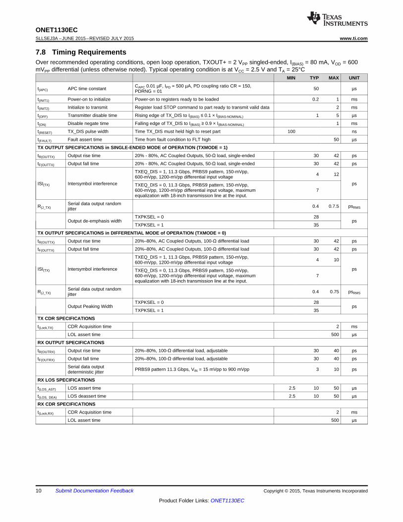
7.8 Timing RequirementsOver recommended operating conditions, open loop operation, TXOUT+ = 2 VPP singled-ended, I(BIAS) = 80 mA, VOD = 600mVPP differential (unless otherwise noted). Typical operating condition is at VCC = 2.5 V and TA = 25°C
MIN TYP MAX UNIT
CAPC 0.01 µF, IPD = 500 µA, PD coupling ratio CR = 150,t(APC) APC time constant 50 µsPDRNG = 01
t(INIT1) Power-on to initialize Power-on to registers ready to be loaded 0.2 1 ms
t(INIT2) Initialize to transmit Register load STOP command to part ready to transmit valid data 2 ms
t(OFF) Transmitter disable time Rising edge of TX_DIS to I(BIAS) ≤ 0.1 × I(BIAS-NOMINAL) 1 5 µs
t(ON) Disable negate time Falling edge of TX_DIS to I(BIAS) ≥ 0.9 × I(BIAS-NOMINAL) 1 ms
t(RESET) TX_DIS pulse width Time TX_DIS must held high to reset part 100 ns
t(FAULT) Fault assert time Time from fault condition to FLT high 50 µs
TX OUTPUT SPECIFICATIONS in SINGLE-ENDED MODE of OPERATION (TXMODE = 1)
tR(OUTTX) Output rise time 20% - 80%, AC Coupled Outputs, 50-Ω load, single-ended 30 42 ps
tF(OUTTX) Output fall time 20% - 80%, AC Coupled Outputs, 50-Ω load, single-ended 30 42 ps
TXEQ_DIS = 1, 11.3 Gbps, PRBS9 pattern, 150-mVpp, 4 12600-mVpp, 1200-mVpp differential input voltageISI(TX) Intersymbol interference psTXEQ_DIS = 0, 11.3 Gbps, PRBS9 pattern, 150-mVpp,
600-mVpp, 1200-mVpp differential input voltage, maximum 7equalization with 18-inch transmission line at the input.
Serial data output randomR(J_TX) 0.4 0.7.5 psRMSjitter
TXPKSEL = 0 28Output de-emphasis width ps
TXPKSEL = 1 35
TX OUTPUT SPECIFICATIONS in DIFFERENTIAL MODE of OPERATION (TXMODE = 0)
tR(OUTTX) Output rise time 20%–80%, AC Coupled Outputs, 100-Ω differential load 30 42 ps
tF(OUTTX) Output fall time 20%–80%, AC Coupled Outputs, 100-Ω differential load 30 42 ps
TXEQ_DIS = 1, 11.3 Gbps, PRBS9 pattern, 150-mVpp, 4 10600-mVpp, 1200-mVpp differential input voltageISI(TX) Intersymbol interference psTXEQ_DIS = 0, 11.3 Gbps, PRBS9 pattern, 150-mVpp,
600-mVpp, 1200-mVpp differential input voltage, maximum 7equalization with 18-inch transmission line at the input.
Serial data output randomR(J_TX) 0.4 0.75 psRMSjitter
TXPKSEL = 0 28Output Peaking Width ps
TXPKSEL = 1 35
TX CDR SPECIFICATIONS
t(Lock,TX) CDR Acquisition time 2 ms
LOL assert time 500 μs
RX OUTPUT SPECIFICATIONS
tR(OUTRX) Output rise time 20%–80%, 100-Ω differential load, adjustable 30 40 ps
tF(OUTRX) Output fall time 20%–80%, 100-Ω differential load, adjustable 30 40 ps
Serial data output PRBS9 pattern 11.3 Gbps, VIN = 15 mVpp to 900 mVpp 3 10 psdeterministic jitter
RX LOS SPECIFICATIONS
t(LOS_AST) LOS assert time 2.5 10 50 μs
t(LOS, DEA) LOS deassert time 2.5 10 50 μs
RX CDR SPECIFICATIONS
t(Lock,RX) CDR Acquisition time 2 ms
LOL assert time 500 μs
10 Submit Documentation Feedback Copyright © 2015, Texas Instruments Incorporated
Product Folder Links: ONET1130EC

tBUF±
tHDSTA
tr
tLOW
tHDDAT
tHIGH
tf
tSUDAT
tSUSTA
tHDSTA
tSUSTO
P S S P
SDA
SCK
ONET1130ECwww.ti.com SLLSEJ3A –JUNE 2015–REVISED JULY 2015
Figure 1. Transmitter Input Sinusoidal Jitter Tolerance (INF-8077i Rev. 4.5 XFP MSA)
Figure 2. 2-Wire Interface Diagram
Copyright © 2015, Texas Instruments Incorporated Submit Documentation Feedback 11
Product Folder Links: ONET1130EC

ONET1130ECSLLSEJ3A –JUNE 2015–REVISED JULY 2015 www.ti.com
Table 1. Timing Diagram DefinitionsSymbol Description Min Max Unit
fSCK SCK clock frequency 400 kHztBUF Bus free time between START and STOP conditions 1.3 µs
Hold time after repeated START condition. After this period, the first clock pulse istHDSTA 0.6 µsgeneratedtLOW Low period of the SCK clock 1.3 µstHIGH High period of the SCK clock 0.6 µstSUSTA Setup time for a repeated START condition 0.6 µstHDDAT Data HOLD time 0 µstSUDAT Data setup time 100 nstR Rise time of both SDA and SCK signals 300 nstF Fall time of both SDA and SCK signals 300 nstSUSTO Setup time for STOP condition 0.6 µs
12 Submit Documentation Feedback Copyright © 2015, Texas Instruments Incorporated
Product Folder Links: ONET1130EC
Modulation Current Register Setting (Decimal)
Ran
dom
Jitt
er (
psrm
s)
0 20 40 60 80 100 120 140 160 180 200 2200
0.1
0.2
0.3
0.4
0.5
0.6
0.7
0.8
0.9
1
D014Free-Air Temperature (°C)
Ran
dom
Jitt
er (
psrm
s)
-40 -20 0 20 40 60 80 1000
0.1
0.2
0.3
0.4
0.5
0.6
0.7
0.8
0.9
1
D015
Free-Air Temperature (°C)
ISI (
psP
P)
-40 -20 0 20 40 60 80 1000
2
4
6
8
D012Free-Air Temperature (°C)
ISI (
psP
P)
-40 -20 0 20 40 60 80 1000
2
4
6
8
D013
TXMOD Register 12 Setting (Decimal)
ISI (
psP
P)
0 20 40 60 80 100 120 140 160 180 2000
1
2
3
4
5
6
7
8
D010TXMOD Register 12 Setting (Decimal)
ISI (
psP
P)
0 20 40 60 80 100 120 140 160 180 2000
1
2
3
4
5
6
7
8
D011
ONET1130ECwww.ti.com SLLSEJ3A –JUNE 2015–REVISED JULY 2015
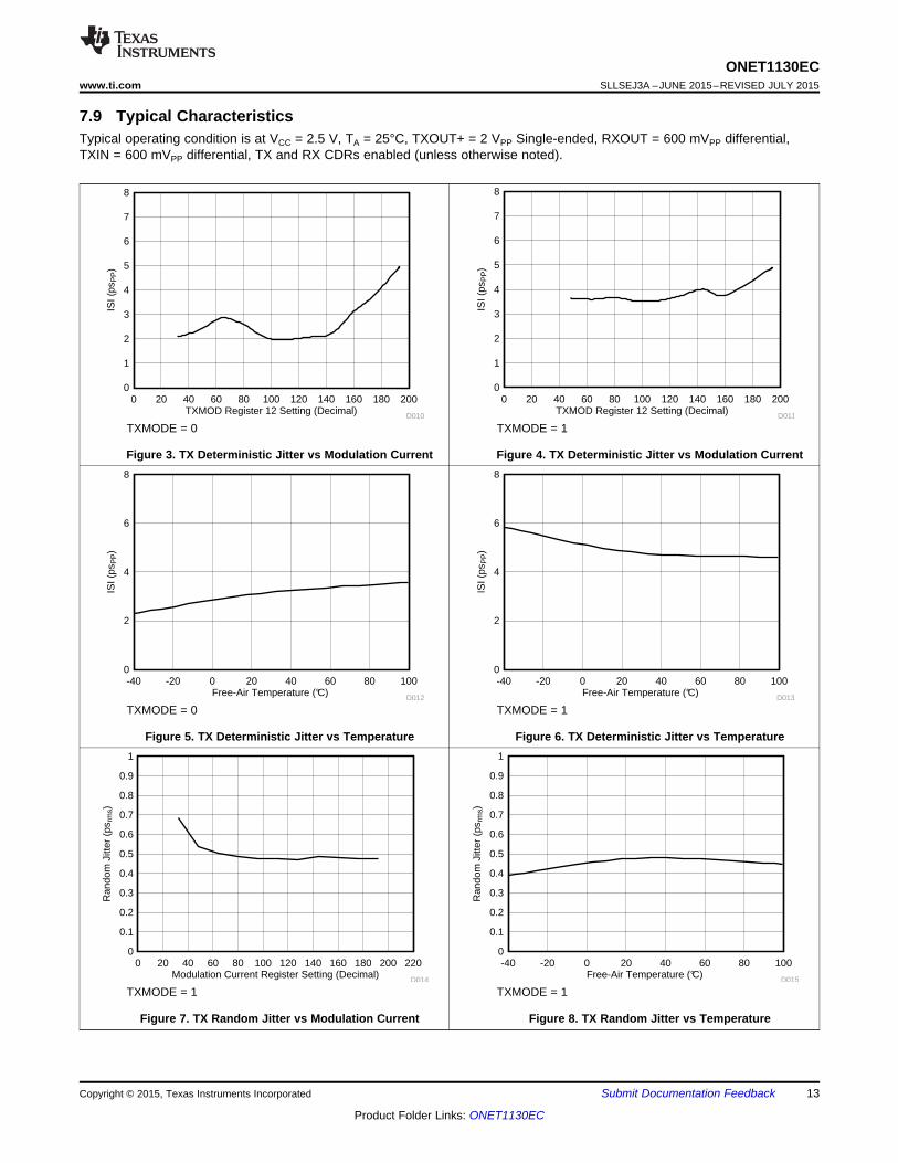
7.9 Typical CharacteristicsTypical operating condition is at VCC = 2.5 V, TA = 25°C, TXOUT+ = 2 VPP Single-ended, RXOUT = 600 mVPP differential,TXIN = 600 mVPP differential, TX and RX CDRs enabled (unless otherwise noted).
TXMODE = 0 TXMODE = 1
Figure 3. TX Deterministic Jitter vs Modulation Current Figure 4. TX Deterministic Jitter vs Modulation Current
TXMODE = 0 TXMODE = 1
Figure 5. TX Deterministic Jitter vs Temperature Figure 6. TX Deterministic Jitter vs Temperature
TXMODE = 1 TXMODE = 1
Figure 7. TX Random Jitter vs Modulation Current Figure 8. TX Random Jitter vs Temperature
Copyright © 2015, Texas Instruments Incorporated Submit Documentation Feedback 13
Product Folder Links: ONET1130EC
Bias Current (mA)
Bia
s M
onito
r C
urre
nt (
mA
)
0 20 40 60 80 100 120 140 160 1800
0.2
0.4
0.6
0.8
1
1.2
1.4
1.6
1.8
D020Photodiode Current (mA)
Pho
todi
ode
Mon
itor
Cur
rent
(m
A)
0 0.1 0.2 0.3 0.4 0.5 0.6 0.7 0.8 0.9 10
0.1
0.2
0.3
0.4
0.5
D021
TXBIAS Register 15 and 16 Setting (Decimal)
Sou
rce
OL
Bia
s C
urre
nt (
mA
)
0 200 400 600 800 1000 12000
20
40
60
80
100
120
140
160
180
D018TXBIAS Register 15 and 16 Setting (Decimal)
Sin
k O
L B
ias
Cur
rent
(m
A)
0 200 400 600 800 1000 12000
20
40
60
80
100
120
140
160
180
D019
TXMOD Register 12 Setting - Decimal
Tra
nsiti
on T
ime
(ps)
0 20 40 60 80 100 120 140 160 180 200 2200
5
10
15
20
25
30
35
40
D016
Rise TimeFall Time
Free-Air Temperature (°C)
Tra
nsiti
on T
ime
(ps)
-40 -20 0 20 40 60 80 1000
5
10
15
20
25
30
35
D017
Rise TimeFall Time
ONET1130ECSLLSEJ3A –JUNE 2015–REVISED JULY 2015 www.ti.com
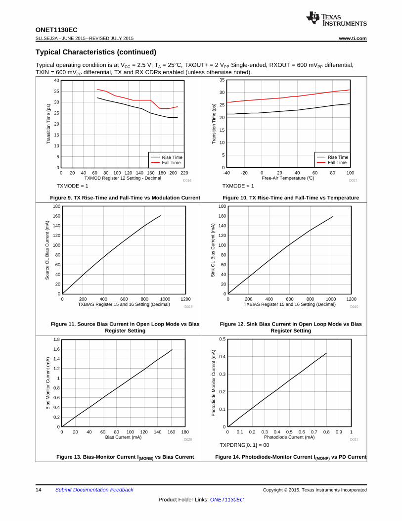
Typical Characteristics (continued)Typical operating condition is at VCC = 2.5 V, TA = 25°C, TXOUT+ = 2 VPP Single-ended, RXOUT = 600 mVPP differential,TXIN = 600 mVPP differential, TX and RX CDRs enabled (unless otherwise noted).
TXMODE = 1 TXMODE = 1
Figure 9. TX Rise-Time and Fall-Time vs Modulation Current Figure 10. TX Rise-Time and Fall-Time vs Temperature
Figure 11. Source Bias Current in Open Loop Mode vs Bias Figure 12. Sink Bias Current in Open Loop Mode vs BiasRegister Setting Register Setting
TXPDRNG[0..1] = 00
Figure 13. Bias-Monitor Current I(MONB) vs Bias Current Figure 14. Photodiode-Monitor Current I(MONP) vs PD Current
14 Submit Documentation Feedback Copyright © 2015, Texas Instruments Incorporated
Product Folder Links: ONET1130EC

TXBMF Register 17 Setting (Decimal)
Bia
s F
ault
Cur
rent
(m
A)
0 50 100 150 200 250 3000
20
40
60
80
100
120
140
160
180
D026TXPMF Register 18 Setting (Decimal)
PD
Fau
lt C
urre
nt (
mA
)
0 50 100 150 200 250 3000
0.2
0.4
0.6
0.8
1
1.2
D027
Free Air Temperature (°C
Sup
ply
Cur
rent
(m
A)
-40 -20 0 20 40 60 80 100220
230
240
250
260
270
280
290
300
D024Free Air Temperature (°C)
Sup
ply
Cur
rent
(m
A)
-40 -20 0 20 40 60 80 100180
190
200
210
220
230
240
250
260
D025
TXMOD Register 12 Setting (Decimal)
Diff
eren
tial O
utpu
t Vol
tage
(V
)
0 20 40 60 80 100 120 140 160 180 200 2200
0.5
1
1.5
2
2.5
3
3.5
4
4.5
D022TXMOD Register 12 Setting (Decimal)
Diff
eren
tial O
utpu
t Vol
tage
(V
)
0 20 40 60 80 100 120 140 160 180 200 2200
0.5
1
1.5
2
2.5
D023
ONET1130ECwww.ti.com SLLSEJ3A –JUNE 2015–REVISED JULY 2015
Typical Characteristics (continued)Typical operating condition is at VCC = 2.5 V, TA = 25°C, TXOUT+ = 2 VPP Single-ended, RXOUT = 600 mVPP differential,TXIN = 600 mVPP differential, TX and RX CDRs enabled (unless otherwise noted).
TXMODE = 0 TXMODE = 1
Figure 15. Output Voltage vs Modulation Current Figure 16. Output Voltage vs Modulation Current
TXMODE = 0 Bias Current = 0 TXMODE = 1 Bias Current = 0
Figure 17. Supply Current vs Temperature Figure 18. Supply Current vs Temperature
Figure 19. Bias Current Monitor Fault vs TXBMF Register Figure 20. Photodiode Current Monitor Fault vs TXPMFSetting Register Setting
Copyright © 2015, Texas Instruments Incorporated Submit Documentation Feedback 15
Product Folder Links: ONET1130EC

Frequency (GHz)
SD
D11
(dB
)
0.1 1 10 100-50
-45
-40
-35
-30
-25
-20
-15
-10
-5
0
D003Frequency (GHz)
SD
D22
(dB
)
0.1 1 10 100-50
-45
-40
-35
-30
-25
-20
-15
-10
-5
0
D004
Frequency (GHz)
SD
D21
(dB
)
0.1 1 10 1000
5
10
15
20
25
30
35
40
45
50
D001Input Voltage (mVPP)
Out
put V
olta
ge (
mV
PP)
0 50 100 150 200 250 3000
100
200
300
400
500
600
700
800
D002
ONET1130ECSLLSEJ3A –JUNE 2015–REVISED JULY 2015 www.ti.com
Typical Characteristics (continued)Typical operating condition is at VCC = 2.5 V, TA = 25°C, TXOUT+ = 2 VPP Single-ended, RXOUT = 600 mVPP differential,TXIN = 600 mVPP differential, TX and RX CDRs enabled (unless otherwise noted).
TXMODE = 0 15 ps/Div TXMODE = 1 15 ps/Div
Figure 21. TX Eye-Diagram at 11.3 Gbps Figure 22. TX Eye-Diagram at 11.3 Gbps
Figure 23. RX Frequency Response (CDR Disabled) Figure 24. RX Transfer Function
Figure 25. RX Differential Input Return Gain vs Frequency Figure 26. RX Differential Output Return Gain vs Frequency
16 Submit Documentation Feedback Copyright © 2015, Texas Instruments Incorporated
Product Folder Links: ONET1130EC

Register Setting (Decimal)
LOS
Ass
ert/D
eass
ert V
olta
ge (
mV
PP)
0 10 20 30 40 500
20
40
60
80
100
120
140
160
D009
LOS Assert VoltageLOS Deassert Voltage
Register Setting (Decimal)
LOS
Hys
tere
sis
(dB
)
0 10 20 30 400
1
2
3
4
5
6
7
8
D028
Input Voltage (mVPP)
Ran
dom
Jitt
er (
psR
MS)
20 30 40 50 60 70 80 90 1000
0.2
0.4
0.6
0.8
1
D007Register Setting (Decimal)
LOS
Ass
ert/D
eass
ert V
olta
ge (
mV
PP)
0 10 20 30 400
20
40
60
80
100
120
140
160
180
200
220
240
260
D008
LOS Assert VoltageLOS Deassert Voltage
Input Voltage (mVPP)
BE
R
SC
OT
T.
0 1 2 3 4 5
1E-12
1E-11
1E-10
1E-9
1E-8
1E-7
1E-6
1E-5
1E-4
1E-3
D005Input Voltage (mVPP)
DJ
(ps P
P)
0 200 400 600 800 1000 1200 1400 1600 1800 20000
1
2
3
4
5
6
7
8
D006
ONET1130ECwww.ti.com SLLSEJ3A –JUNE 2015–REVISED JULY 2015
Typical Characteristics (continued)Typical operating condition is at VCC = 2.5 V, TA = 25°C, TXOUT+ = 2 VPP Single-ended, RXOUT = 600 mVPP differential,TXIN = 600 mVPP differential, TX and RX CDRs enabled (unless otherwise noted).
11.3 Gbps TX Disabled
Figure 27. RX Bit-Error Ratio vs Input Amplitude Figure 28. RX Deterministic Jitter vs Input Amplitude
RX LOSRNG = 0
Figure 29. RX Random Jitter vs Input Amplitude Figure 30. LOS Assert / Deassert Voltage vs Register 7Setting
RX LOSRNG = 1 RX LOSRNG = 0
Figure 31. LOS Assert / Deassert Voltage vs Register 7 Figure 32. LOS Hysteresis vs Register 7 SettingSetting
Copyright © 2015, Texas Instruments Incorporated Submit Documentation Feedback 17
Product Folder Links: ONET1130EC
Register Setting (Decimal)
LOS
Hys
tere
sis
(dB
)
0 10 20 30 40 500
1
2
3
4
5
6
7
8
D028
ONET1130ECSLLSEJ3A –JUNE 2015–REVISED JULY 2015 www.ti.com
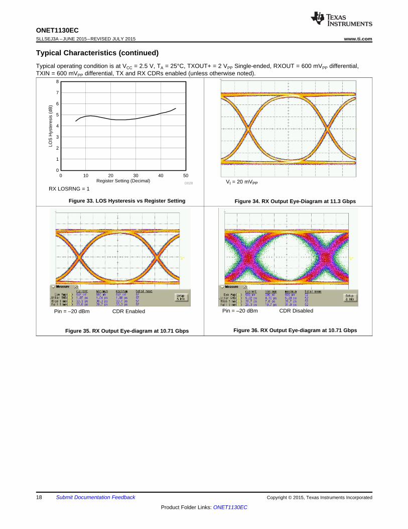
Typical Characteristics (continued)Typical operating condition is at VCC = 2.5 V, TA = 25°C, TXOUT+ = 2 VPP Single-ended, RXOUT = 600 mVPP differential,TXIN = 600 mVPP differential, TX and RX CDRs enabled (unless otherwise noted).
VI = 20 mVPPRX LOSRNG = 1
Figure 33. LOS Hysteresis vs Register Setting Figure 34. RX Output Eye-Diagram at 11.3 Gbps
Pin = –20 dBm CDR DisabledPin = –20 dBm CDR Enabled
Figure 36. RX Output Eye-diagram at 10.71 GbpsFigure 35. RX Output Eye-diagram at 10.71 Gbps
18 Submit Documentation Feedback Copyright © 2015, Texas Instruments Incorporated
Product Folder Links: ONET1130EC

ONET1130ECwww.ti.com SLLSEJ3A –JUNE 2015–REVISED JULY 2015
8 Detailed Description
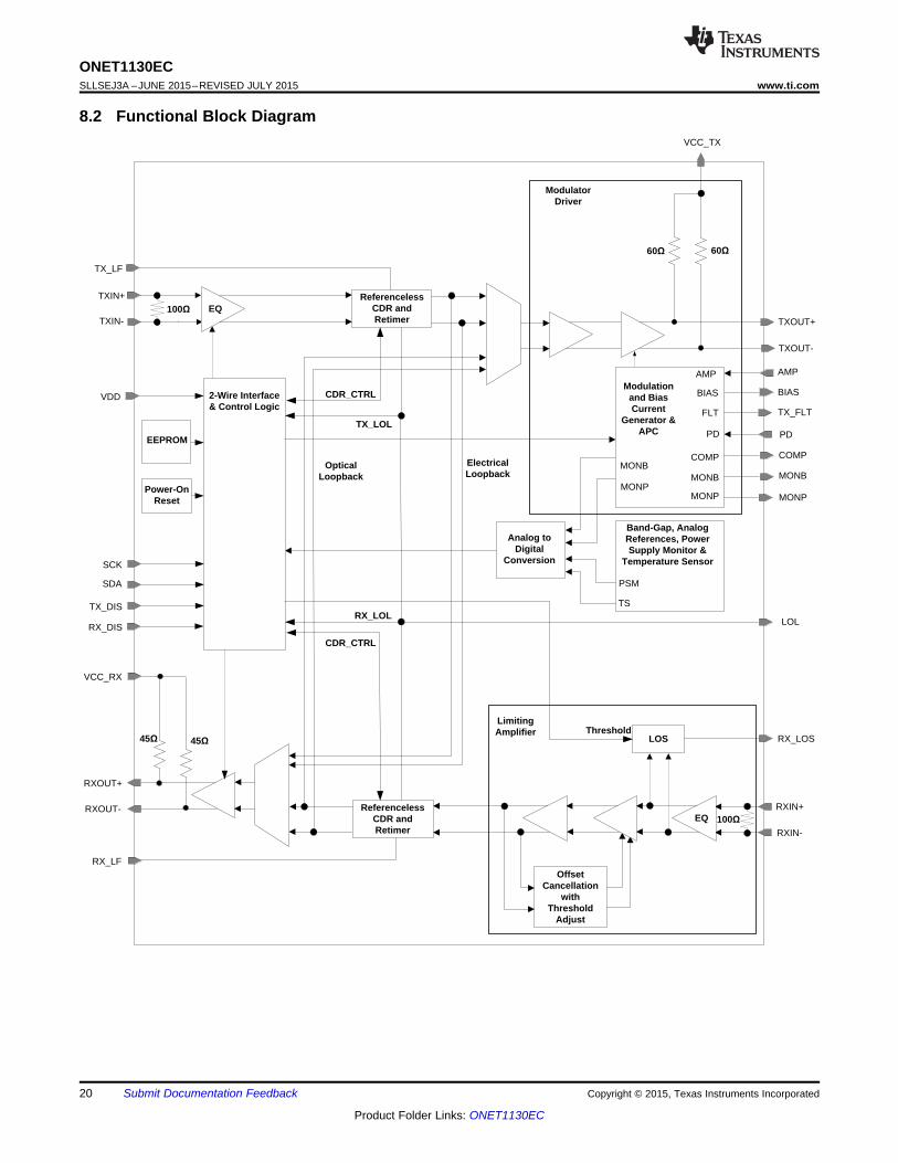
8.1 OverviewA simplified block diagram of the ONET1130EC is shown in Functional Block Diagram.
The ONET1130EC consists of a transmitter path, a receiver path, an analog reference block, an analog to digitalconverter and a 2-wire serial interface and control logic block with power-on reset.
The transmit path consists of an adjustable input equalizer, a multi-rate CDR and an output modulator driver. Theoutput driver provides a differential output voltage but can be operated in a single-ended mode to reduce thepower consumption. Output waveform control, in the form of cross-point adjustment and de-emphasis areavailable to improve the optical eye mask margin. Bias current for the laser is provided and an integratedautomatic power control (APC) loop to compensate for variations in average optical power over voltage,temperature and time is included.
The receive path consists of a limiting amplifier with programmable equalization and threshold adjustment, amulti-rate CDR and an output driver with de-emphasis to compensate for frequency dependent loss ofconnectors and transmission lines. The receiver output amplitude, de-emphasis and loss of signal assert levelcan be adjusted.
The ONET1130EC contains an analog to digital converter to support transceiver digital diagnostics and canreport the supply voltage, laser bias current, laser photodiode current and internal temperature.
The 2-wire serial interface is used to control the operation of the device and read the status of the controlregisters.
The device contains internal EEPROM for trimming purposes only.
Copyright © 2015, Texas Instruments Incorporated Submit Documentation Feedback 19
Product Folder Links: ONET1130EC
TX_DIS
TXIN+
TXIN-
SCK
SDA
LOS
Offset Cancellation
with Threshold
Adjust
RX_LOS
RXIN+
RXIN-
RXOUT+
RXOUT-
ThresholdLimiting Amplifier
ReferencelessCDR and Retimer
100
Referenceless CDR and Retimer
Band-Gap, Analog References, Power Supply Monitor &
Temperature Sensor
Analog to Digital
Conversion
TS
PSM
2-Wire Interface & Control Logic
Optical Loopback
RX_LOL
CDR_CTRL
TX_LOL
CDR_CTRL
Electrical Loopback
EQ
TX_LF
RX_LF
LOL
Power-On Reset
EEPROM
VDD
RX_DIS
VCC_RX
100
EQ
45 45
TXOUT+
TXOUT-
BIAS
PD
Modulator Driver
TX_FLT
Modulation and Bias Current
Generator & APC
MONB
MONP
FLT
PD
BIAS
MONB
MONP
VCC_TX
MONB
MONP
COMPCOMP
AMPAMP
60 60
ONET1130ECSLLSEJ3A –JUNE 2015–REVISED JULY 2015 www.ti.com
8.2 Functional Block Diagram
20 Submit Documentation Feedback Copyright © 2015, Texas Instruments Incorporated
Product Folder Links: ONET1130EC

ONET1130ECwww.ti.com SLLSEJ3A –JUNE 2015–REVISED JULY 2015
8.3 Feature Description
8.3.1 Transmitter
8.3.1.1 EqualizerThe data signal is applied to an input equalizer by means of the input signal pins TXIN+ / TXIN–, which provideon-chip differential 100-Ω line termination. The equalizer is enabled by default and can be disabled by setting thetransmitter equalizer disable bit TXEQ_DIS = 1 (bit 1 of register 10). Equalization of up to 300 mm (12 inches) ofmicrostrip or stripline transmission line on FR4 printed circuit boards can be achieved. The amount ofequalization is set through register settings TXCTLE [0..3] (register 11). The device can accept input amplitudelevels from 100 mVpp up to 1000 mVpp.
8.3.1.2 CDRThe clock and data recovery function consists of a Phase-Locked Loop (PLL) and retimer. The CDR can beoperated without a reference clock and the Voltage Controlled Oscillator (VCO) can cover 9.8 Gbps to 11.7 Gbpsdata rates. The PLL is phase locked to the incoming data stream and attenuates the high frequency jitter on thedata, producing a recovered clean clock with substantially reduced jitter. An external capacitor for the PLL loopfilter is connected to the TX_LF pin. A value of 2.2 nF is recommended. The clean clock is used to retime theincoming data, producing an output signal with reduced jitter, and in effect, resetting the jitter budget for thetransmitter.
The CDR is enabled by default. The CDR can be disabled and bypassed by setting the transmitter CDR disablebit TXCDR_DIS = 1 (bit 4 of register 10). Alternatively, the CDR can be left powered on but bypassed by settingthe transmitter CDR bypass bit TX_CDRBP = 1 (bit 3 of register 10); however, this function only works if thereceiver CDR bypass bit RX_CDRBP (bit 3 of register 4) is also set to 1.
The CDR is designed to meet the XFP Datacom requirements and Telecom requirements for a maximum of 1-dBjitter peaking at a frequency greater than 120 kHz. The CDR is not designed to meet the Telecom regeneratorrequirements of jitter peaking less than 0.03 dB at a frequency less than 120 kHz. The default CDR bandwidth istypically 4.5 MHz and can be adjusted using the SEL_RES[0..2] bits (bits 5 to 7 of register 51). Adjusting thesebits changes the bandwidth of both the transmitter and receiver CDRs.
For the majority of applications, the default settings in register 19 for the transmitter CDR can be used. However,for some applications or for test purposes, some modes of operation may be useful. The frequency detector forthe PLL is set to an automatic mode of operation by default. When a signal is applied to the transmitter input thefrequency detector search algorithm will be initiated to determine the frequency of the data. The default algorithmensures a fast CDR lock time of less than 2 ms. The fast lock can be disabled by setting the transmitter CDR fastlock disable bit TXFL_DIS = 1 (bit 3 of register 19). Once the frequency has been detected then the frequencydetector will be disabled and the supply current will decrease by approximately 10mA. In some applications, suchas when there are long periods of idle data, it may be advantageous to keep the frequency detector permanentlyenabled by setting the transmitter frequency detector enable bit TXFD_EN = 1 (bit 5 of register 19). For testpurposes, the frequency detector can be permanently disabled by setting the transmitter frequency detectordisable bit TXFD_DIS = 1 (bit 4 of register 19). For fast lock times the frequency detector can be set to one oftwo preselected data rates using the transmitter frequency detection mode selection bits TXFD_MOD[0..1] (bits 6and 7 of register 19). If it is desired to use the retimer at lower data rates than the standard 9.8 to 11.7Gbps thenthe transmitter divider ratio should be adjusted accordingly through TXDIV[0..2] (bits 0 to 2 of register 19). Forexample, for re-timed operation at 2.5 Gbps the divider should be set to divide by 4.
8.3.1.3 Modulator DriverThe modulation current is sunk from the common emitter node of the limiting output driver differential pair bymeans of a modulation current generator, which is digitally controlled by the 2-wire serial interface.
The collector nodes of the output stages are connected to the transmitter output pins TXOUT+ and TXOUT–.The collectors have internal 50Ω back termination resistors to VCC_TX. The outputs are optimized to drive a 50Ω single-ended load and to obtain the maximum single-ended output voltage of 2.0Vpp, AC coupling andinductive pull-ups to VCC are required. For reduced power consumption the DC resistance of the inductive pull-ups should be minimized to provide sufficient headroom on the TXOUT+ and TXOUT– pins.
Copyright © 2015, Texas Instruments Incorporated Submit Documentation Feedback 21
Product Folder Links: ONET1130EC

Transmitter De-EmphasisRegister 13 Bit 5 = 0
Transmitter De-EmphasisRegister 13 Bit 5 = 1
Register 13 Bits 0±3
Register 13 Bits 0±3
Register 11 Bit 6
Register 11 Bit 6
ONET1130ECSLLSEJ3A –JUNE 2015–REVISED JULY 2015 www.ti.com
Feature Description (continued)The polarity of the output pins can be inverted by setting the transmitter output polarity switch bit, TXOUTPOL(bit 5 of register 10) to 1. In addition, the output driver can be disabled by setting the transmitter output driverdisable bit TXOUT_DIS = 1 (bit 6 of register 10).
The output driver is set to differential output by default. In order to reduce the power consumption for single-ended applications driving an electroabsorptive modulated laser (EML) the output drive register 13 should be setto single-ended mode. The single-ended output signal is enabled by setting the transmitter mode select bitTXMODE = 1 (bit 6 of register 13). The positive output is active by default. To enable the negative output anddisable the positive output set TXOUTSEL = 1 (bit 7 of register 13).
Output de-emphasis can be applied to the signal by adjusting the transmitter de-emphasis bits TXDEADJ[0..3](bits 0 to 3 of register 13). In addition, the width of the applied de-emphasis can be increased by setting thetransmitter output peaking width TXPKSEL = 1 (bit 6 of register 11). The wide peaking width would typically beuseful for a more capacitive transmitter load. How de-emphasis is applied is controlled through the TXSTEP bit(bit 5 of register 13). Setting TXSTEP = 1 delays the time of the applied de-emphasis and has more of an impacton the falling edge. A graphical representation of the two de-emphasis modes is shown in Figure 37. Using de-emphasis can help to optimize the transmitted output signal; however, it will add to the power consumption.
The output edge speed can be set to slow mode of operation through the TXSLOW bit (bit 4 of register 13). Fortransmitter modulation output settings (TXMOD - register 12) below 0xC0 it is recommended to set TXSLOW = 1to reduce the output jitter.
Figure 37. Transmitter De-Emphasis Modes
8.3.1.4 Modulation Current GeneratorThe modulation current generator provides the current for the high speed output driver described above. Thecircuit can be digitally controlled through the 2-wire interface block or controlled by applying an analog voltage inthe range of 0 to 2V to the AMP pin. The default method of control is through the 2-wire interface. To use theAMP pin set the transmitter amplitude control bit TXAMPCTRL = 1 (bit 0 of register 10).
An 8-bit wide control bus, TXMOD[0..7] (register 12), is used to set the desired modulation current and the outputvoltage.
The entire transmitter signal path, including CDR, can be disabled and powered down by setting TX_DIS = 1 (bit7 of register 10).
22 Submit Documentation Feedback Copyright © 2015, Texas Instruments Incorporated
Product Folder Links: ONET1130EC

ONET1130ECwww.ti.com SLLSEJ3A –JUNE 2015–REVISED JULY 2015
Feature Description (continued)8.3.1.5 DC Offset Cancellation and Cross Point ControlThe ONET1130EC transmitter has DC offset cancellation to compensate for internal offset voltages. The offsetcancellation can be disabled by setting TXOC_DIS = 1 (bit 2 of register 10).
The crossing point can be moved toward the one level by setting TXCPSGN = 1 (bit 7 of register 14) and it canbe moved toward the zero level by setting TXCPSGN = 0. The percentage of shift depends upon the registersettings of the transmitter cross-point adjustment bits TXCPADJ[0..6] (register 14).
8.3.1.6 Transmitter Loopback (Electrical Loopback)The signal input to the TXIN+ and TXIN– pins can be looped back to the receiver output after the retimer asshown in Figure 38 by setting TX_LBMUX = 1 (bit 0 of register 2). Loopback from the receiver input to thetransmitter output (optical loopback) can be enabled at the same time.
If it is desired to loopback the signal input to the TXIN+ and TXIN– pins to the receiver output with the CDRdisabled then the transmit CDR must be disabled and bypassed by setting TXCDR_DIS = 1 (bit 4 of register 10)and the receiver CDR must also be disabled and bypassed by setting RXCDR_DIS =1 (bit 4 of register 4).
Copyright © 2015, Texas Instruments Incorporated Submit Documentation Feedback 23
Product Folder Links: ONET1130EC

TX_DIS
TXIN+
TXIN-
SCK
SDA
LOS
Offset Cancellation
with Threshold
Adjust
RX_LOS
RXIN+
RXIN-
RXOUT+
RXOUT-
ThresholdLimiting Amplifier
ReferencelessCDR and Retimer
100
Referenceless CDR and Retimer
Band-Gap, Analog References, Power Supply Monitor &
Temperature Sensor
Analog to Digital
Conversion
TS
PSM
2-Wire Interface & Control Logic
Optical Loopback
RX_LOL
CDR_CTRL
TX_LOL
CDR_CTRL
Electrical Loopback
EQ
TX_LF
RX_LF
LOL
Power-On Reset
EEPROM
VDD
RX_DIS
VCC_RX
100
EQ
45 45
TXOUT+
TXOUT-
BIAS
PD
Modulator Driver
TX_FLT
Modulation and Bias Current
Generator & APC
MONB
MONP
FLT
PD
BIAS
MONB
MONP
MONB
MONP
COMPCOMP
AMPAMP
VCC_TX
60 60
ONET1130ECSLLSEJ3A –JUNE 2015–REVISED JULY 2015 www.ti.com
Feature Description (continued)
Figure 38. Electrical Loopback
24 Submit Documentation Feedback Copyright © 2015, Texas Instruments Incorporated
Product Folder Links: ONET1130EC

ONET1130ECwww.ti.com SLLSEJ3A –JUNE 2015–REVISED JULY 2015
Feature Description (continued)8.3.1.7 Bias Current Generation and APC LoopThe bias current for the laser is turned off by default and has to be enabled by setting the laser bias currentenable bit TXBIASEN = 1 (bit 2 of register 1). In open loop operation, selected by setting TXOLENA = 1 (bit 4 ofregister 1), the bias current is set directly by the 10-bit wide control word TXBIAS[0..9] (register 15 and register16). In Automatic Power Control (APC) mode, selected by setting TXOLENA = 0, the bias current depends onthe register settings TXBIAS[0..9] and the coupling ratio (CR) between the laser bias current and the photodiodecurrent. CR = IBIAS/IPD. If the photodiode cathode is connected to VCC and the anode is connected to the PD pin(PD pin is sinking current) set TXPDPOL = 1 (bit 0 of register 1). If the photodiode anode is connected to groundand the cathode is connected to the PD pin (PD pin is sourcing current), set TXPDPOL = 0.
Three photodiode current ranges can be selected by means of the photodiode current range bits TXPDRNG[0..1](bits 5 and 6 of register 1). The photodiode range should be chosen to keep the laser bias control DAC,TXBIAS[0..9], close to the center of its range. This keeps the laser bias current set point resolution high. Fordetails regarding the bias current setting in open-loop mode as well as in closed-loop mode, see the RegisterMapping table.
The ONET1130EC has the ability to source or sink the bias current. The default condition is for the BIAS pin tosource the current (TXBIASPOL = 0). To act as a sink, set TXBIASPOL = 1 (bit 1 of register 1).
The bias current is monitored using a current mirror with a gain equal to 1/100. By connecting a resistor betweenMONB and GND, the bias current can be monitored as a voltage across the resistor. A low temperaturecoefficient precision resistor should be used. The bias current can also be monitored as a 10 bit unsigned digitalword by setting the transmitter bias current digital monitor selection bit TXDMONB = 1 (bit 5 of register 16) andremoving the resistor from MONB to ground.
The photodiode current is monitored using a current mirror with various gains that are dependent upon thephotodiode current range being used. By connecting a resistor between MONP and GND, the photodiode currentcan be monitored as a voltage across the resistor. A low temperature coefficient precision resistor should beused. The photodiode current can also be monitored as a 10 bit unsigned digital word by setting the transmitterphotodiode current digital monitor selection bit TXDMONP = 1 (bit 6 of register 16) and removing the resistorfrom MONP to ground.
8.3.1.8 Laser Safety Features and Fault Recovery ProcedureThe ONET1130EC provides built in laser safety features. The following fault conditions are detected if thetransmitter fault detection enable bit TXFLTEN = 1 (bit 3 of register 1):1. Voltage at MONB exceeds the bandgap voltage (1.2 V) or, alternately, if TXDMONB = 1 and the bias current
exceeds the bias current monitor fault threshold set by TXBMF[0..7] (register 17). When using the digitalmonitor, the resistor from the MONB pin to ground must be removed.
2. Voltage at MONP exceeds the bandgap voltage (1.2 V) and the analog photodiode current monitor faulttrigger bit, TXMONPFLT (bit 7 of register 1), is set to 1. Alternately, a fault can be triggered if TXDMONP = 1and the photodiode current exceeds the photodiode current monitor fault threshold set by TXPMF[0..7](register 18). When using the digital monitor, the resistor from the MONP pin to ground must be removed.
3. Photodiode current exceeds 150% of its set value,4. Bias control DAC drops in value by more than 50% in one step.
If the fault detection is being used then to avoid a fault from occurring at start-up it is recommended to set up therequired bias current and APC loop conditions first and enable the laser bias current (TXBIASEN = 1) as the laststep in the sequence of commands.
If one or more fault conditions occur and the transmitter fault enable bit TXFLTEN is set to 1, the ONET1130ECresponds by:1. Setting the bias current to zero.2. Asserting and latching the TX_FLT pin.3. Setting the TX_FLT bit (bit 5 of register 43) to 1.
Fault recovery is performed by the following procedure:1. The transmitter disable pin TX_DIS and/or the transmitter bias current enable bit TXBIASEN are toggled for
at least the fault latch reset time.
Copyright © 2015, Texas Instruments Incorporated Submit Documentation Feedback 25
Product Folder Links: ONET1130EC

ONET1130ECSLLSEJ3A –JUNE 2015–REVISED JULY 2015 www.ti.com
Feature Description (continued)2. The TX_FLT pin de-asserts while the transmitter disable pin TX_DIS is asserted or the transmitter bias
current enable bit TXBIASEN is de-asserted.3. If the fault condition is no longer present, the part will return to normal operation with its prior output settings
after the disable negate time.4. If the fault condition is still present, TX_FLT re-asserts once TX_DIS is set to a low level and/or TXBIASEN is
set to 0 and the part will not return to normal operation.
8.3.2 Receiver
8.3.2.1 EqualizerThe data signal is applied to an input equalizer by means of the input signal pins RXIN+ / RXIN–, which provideon-chip differential 100 Ω line-termination. The equalizer is enabled by default and can be disabled by setting thereceiver equalizer disable bit RXEQ_DIS = 1 (bit 1 of register 4). Equalization is provided for bandwidthcompensation of the optical receiver. The amount of equalization is set through the register settings RXCTLE[0..2] (register 5). The device can accept input amplitude levels from 6 mVpp up to 800 mVpp.
8.3.2.2 DC Offset Cancellation and Cross Point ControlReceiver offset cancellation compensates for internal offset voltages and thus ensures proper operation even forvery small input data signals. The offset cancellation is enabled by default and the input threshold voltage can beadjusted using register settings RXTHADJ[0..3] (register 6) to optimize the bit error rate or change the eyecrossing point to compensate for input signal pulse width distortion. The offset cancellation can be disabled bysetting RXOC_DIS = 1 (bit 2 of register 4) and this also disables the cross point adjustment.
8.3.2.3 CDRThe receiver clock and data recovery function consists of a Phase-Locked Loop (PLL) and retimer. The CDR canbe operated without a reference clock and the Voltage Controlled Oscillator (VCO) can cover 9.8Gbps to 11.7Gbps data rates. The PLL is phase locked to the incoming data stream and attenuates the high frequency jitteron the data, producing a recovered clean clock with substantially reduced jitter. An external capacitor for the PLLloop filter is connected to the RX_LF pin. A value of 2.2 nF is recommended. The clean clock is used to retimethe incoming data, producing an output signal with reduced jitter, and in effect, resetting the jitter budget for thereceiver.
The CDR is enabled by default. The CDR can be disabled and bypassed by setting the receiver CDR disable bitRXCDR_DIS = 1 (bit 4 of register 4). Alternatively, the CDR can be left powered on but bypassed by setting thereceiver CDR bypass bit RX_CDRBP = 1 (bit 3 of register 4); however, this only works if the transmitter CDRbypass bit TX_CDRBP (bit 3 of register 10) is also set to 1.
The CDR is designed to meet the XFP Datacom requirements and Telecom requirements for a maximum of 1 dBjitter peaking at a frequency greater than 120 kHz. The CDR is not designed to meet the Telecom regeneratorrequirements of jitter peaking less than 0.03 dB at a frequency less than 120 kHz.The default CDR bandwidth istypically 4.5 MHz and can be adjusted using the SEL_RES[0..2] bits (bits 5 to 7 of register 51). Adjusting thesebits changes the bandwidth of both the receiver and transmitter CDRs.
For the majority of applications the default settings in register 9 for the receiver CDR can be used. However, forsome applications or for test purposes, some modes of operation may be useful. The frequency detector for thePLL is set to an automatic mode of operation by default. When a signal is applied to the receiver input thefrequency detector search algorithm will be initiated to determine the frequency of the data. The default algorithmensures a fast CDR lock time of less than 2 ms. The fast lock can be disabled by setting the receiver CDR fastlock disable bit RXFL_DIS = 1 (bit 3 of register 9). Once the frequency has been detected then the frequencydetector will be disabled and the supply current will decrease by approximately 10 mA. In some applications,such as when there are long periods of idle data, it may be advantageous to keep the frequency detectorpermanently enabled by setting the receiver frequency detector enable bit RXFD_EN = 1 (bit 5 of register 9). Fortest purposes, the frequency detector can be permanently disabled by setting the receiver frequency detector
26 Submit Documentation Feedback Copyright © 2015, Texas Instruments Incorporated
Product Folder Links: ONET1130EC

ONET1130ECwww.ti.com SLLSEJ3A –JUNE 2015–REVISED JULY 2015
Feature Description (continued)disable bit RXFD_DIS = 1 (bit 4 of register 9). For fast lock times the frequency detector can be set to one of twopreselected data rates using the receiver frequency detection mode selection bits RXFD_MOD[0..1] (bits 6 and 7of register 9). If it is desired to use the retimer at lower data rates than the standard 9.8 to 11.7 Gbps then thereceiver divider ratio should be adjusted accordingly through RXDIV[0..2] (bits 0 to 2 of register 9). For example,for retimed operation at 2.5 Gbps the divider should be set to divide by 4.
8.3.2.4 Output DriverThe output amplitude of the driver can be varied from 300 mVpp to 900 mVpp using the register settingsRXAMP[0..3] (register 8). The default amplitude setting is 300 mVpp. To compensate for frequency dependentlosses of transmission lines connected to the output, adjustable de-emphasis is provided. The de-emphasis canbe adjusted using RXDADJ[0..2] (register 8). The polarity of the output pins can be inverted by setting thereceiver output polarity switch bit RXOUTPOL = 1 (bit 5 of register 4).
In addition, the output driver can be disabled by setting the receiver output driver disable bit RXOUT_DIS = 1 (bit6 of register 4) or the receiver signal path can be disabled and powered down by setting RX_DIS = 1 (bit 7 ofregister 4).
8.3.2.5 Receiver Loopback (Optical Loopback)The signal input to the RXIN+ and RXIN– pins can be looped back to the transmitter output after the retimer asshown in Figure 39 by setting RX_LBMUX = 1 (bit 1 of register 2). Loopback from the transmitter input to thereceiver output (electrical loopback) can be enabled at the same time.
If it is desired to loopback the signal input to the RXIN+ and RXIN– pins to the transmitter output with the CDRdisabled then the receive CDR must be disabled and bypassed by setting RXCDR_DIS = 1 (bit 4 of register 4)and the transmit CDR must also be disabled and bypassed by setting TXCDR_DIS =1 (bit 4 of register 10).
Copyright © 2015, Texas Instruments Incorporated Submit Documentation Feedback 27
Product Folder Links: ONET1130EC

TX_DIS
TXIN+
TXIN-
SCK
SDA
LOS
Offset Cancellation
with Threshold
Adjust
RX_LOS
RXIN+
RXIN-
RXOUT+
RXOUT-
ThresholdLimiting Amplifier
ReferencelessCDR and Retimer
100
Referenceless CDR and Retimer
Band-Gap, Analog References, Power Supply Monitor &
Temperature Sensor
Analog to Digital
Conversion
TS
PSM
2-Wire Interface & Control Logic
Optical Loopback
RX_LOL
CDR_CTRL
TX_LOL
CDR_CTRL
Electrical Loopback
EQ
TX_LF
RX_LF
LOL
Power-On Reset
EEPROM
VDD
RX_DIS
VCC_RX
100
EQ
45 45
TXOUT+
TXOUT-
BIAS
PD
Modulator Driver
TX_FLT
Modulation and Bias Current
Generator & APC
MONB
MONP
FLT
PD
BIAS
MONB
MONP
MONB
MONP
COMPCOMP
AMPAMP
VCC_TX
60 60
ONET1130ECSLLSEJ3A –JUNE 2015–REVISED JULY 2015 www.ti.com
Feature Description (continued)
Figure 39. Optical Loopback
28 Submit Documentation Feedback Copyright © 2015, Texas Instruments Incorporated
Product Folder Links: ONET1130EC
ONET1130ECwww.ti.com SLLSEJ3A –JUNE 2015–REVISED JULY 2015
Feature Description (continued)8.3.2.6 Loss of Signal DetectionThe loss of signal (LOS) detection is done by 2 separate level detectors to cover a wide dynamic range. Thepeak values of the input signal are monitored by a peak detector and compared to a pre-defined loss of signalthreshold voltage inside the loss of signal detection block. As a result of the comparison, the LOS signal, whichindicates that the input signal amplitude is below the defined threshold level, is generated. There are 2 LOSranges settable with the RXLOSRNG bit (bit 0 of register 4). With RXLOSRNG = 0 the high range of the LOSassert values are used (40 mVPP to 130 mVPP) and by setting RXLOSRNG = 1 the low range of the LOS assertvalues are used (10 mVPP to 50 mVPP). There are 64 possible internal LOS settings set with RXLOSA[0..5](register 7) for each LOS range to adjust the LOS assert level.
The typical LOS hysteresis, as defined by 20log(LOS de-assert voltage/LOS assert voltage) is 4 dB. This can bereduced by approximately 2 dB by setting receiver hysteresis RXHYS = 1 (bit 7 of register 6). In addition, theLOS detection time can be reduced by setting the receiver fast LOS bit RXFLOS = 1 (bit 3 of register 5);however, this may result in chatter (LOS bounce).
8.3.3 Analog Block
8.3.3.1 Analog Reference and Temperature SensorThe ONET1130EC is supplied by a single 2.5 V ±5% supply voltage connected to the VCC_TX, VCC_RX andVDD pins. This voltage is referred to ground (GND) and can be monitored as a 10 bit unsigned digital wordthrough the 2-wire interface.
On-chip bandgap voltage circuitry generates a reference voltage, independent of the supply voltage, from whichall other internally required voltages and bias currents are derived.
In order to minimize the module component count, the ONET1130ECprovides an on-chip temperature sensor.The temperature can be monitored as a 10 bit unsigned digital word through the 2-wire interface.
8.3.3.2 Power-On ResetThe ONET1130EC has power on reset circuitry which ensures that all registers are reset to default values duringstartup. After the power-on to initialize time (tINIT1), the internal registers are ready to be loaded. The part is readyto transmit data after the initialize to transmit time (tINIT2), assuming that the enable chip bit EN_CHIP = 1 (bit 0 ofregister 0). In addition, the transmitter disable pin TX_DIS and receiver disable pin RX_DIS must be set to zero.
The ONET1130EC bias current can be disabled by setting the TX_DIS pin high. The internal registers are notreset. After the transmitter disable pin TX_DIS is set low the part returns to its prior output settings.
8.3.3.3 Analog to Digital ConverterThe ONET1130EC has an internal 10 bit analog to digital converter (ADC) that converts the analog monitors fortemperature, power supply voltage, bias current and photodiode current into a 10 bit unsigned digital word. Thefirst 8 most significant bits (MSBs) are available in register 40 and the 2 least significant bits (LSBs) are availablein register 41. Depending on the accuracy required, 8 bits or 10 bits can be read. However, due to thearchitecture of the 2-wire interface, in order to read the 2 registers, 2 separate read commands have to be sent.
The ADC is enabled by default so to monitor a particular parameter, select the parameter with ADCSEL[0..2](bits 0 to 2 of register 3). Table 2 shows the ADCSEL bits and the parameter that is monitored.
Table 2. ADC Selection Bits and the Monitored ParameterADCSEL2 ADCSEL1 ADCSEL0 MONITORED PARAMETER
0 0 0 Temperature0 0 1 Supply voltage0 1 0 Bias current0 1 1 Photodiode current
Copyright © 2015, Texas Instruments Incorporated Submit Documentation Feedback 29
Product Folder Links: ONET1130EC

ONET1130ECSLLSEJ3A –JUNE 2015–REVISED JULY 2015 www.ti.com
To digitally monitor the photodiode current, ensure that TXDMONP = 1 (bit 6 of register 16) and that a resistor isnot connected to the MONP pin. To digitally monitor the bias current, ensure that TXDMONB = 1 (bit 5 of register16) and that a resistor is not connected to the MONB pin. The ADC is disabled by default. To enable the ADC,set the ADC oscillator enable bit OSCEN = 1 (bit 6 of register 3) and set the ADC enable bit ADCEN = 1 (bit 7 ofregister 3).
The digital word read from the ADC can be converted to its analog equivalent through the following formulas.Temperature (°C) = (0.5475 × ADCx) – 273 (1)Power supply voltage (V) = (1.36m × ADCx) + 1.76 (2)IPD(μA) = 2 x [ (0.62 × ADCx) – 16] for TXPDRNG00 (3)IPD(μA) = 4 x [ (0.62 × ADCx) – 16] for TXPDRNG01 (4)IPD(μA) = 8 x [ (0.62 × ADCx) – 16] for TXPDRNG1x (5)IBIAS (mA) = (0.2 × ADCx) – 4.5 (6)
Where: ADCx = the decimal value read from the ADC
8.3.3.4 2-Wire Interface and Control LogicThe ONET1130EC uses a 2-wire serial interface for digital control. The two circuit inputs, SDA and SCK, aredriven, respectively, by the serial data and serial clock from a microprocessor, for example. The SDA and SCKpins require external 4.7-kΩ to 10-kΩ pull-up resistor to VCC for proper operation.
The 2-wire interface allows write access to the internal memory map to modify control registers and read accessto read out the control signals. The ONET1130EC is a slave device only which means that it cannot initiate atransmission itself; it always relies on the availability of the SCK signal for the duration of the transmission. Themaster device provides the clock signal as well as the START and STOP commands. The protocol for a datatransmission is as follows:1. START command2. Seven (7) bit slave address (0001000) followed by an eighth bit which is the data direction bit (R/W). A zero
indicates a WRITE and a 1 indicates a READ.3. 8 bit register address4. 8 bit register data word5. STOP command
Regarding timing, the ONET1130EC is I2C compatible. The typical timing is shown in Figure 2 and a completedata transfer is shown in Figure 40. Parameters for Figure 2 are defined in Table 1.
8.3.3.5 Bus IdleBoth SDA and SCK lines remain HIGH
8.3.3.6 Start Data TransferA change in the state of the SDA line, from HIGH to LOW, while the SCK line is HIGH, defines a STARTcondition (S). Each data transfer is initiated with a START condition.
8.3.3.7 Stop Data TransferA change in the state of the SDA line from LOW to HIGH while the SCK line is HIGH defines a STOP condition(P). Each data transfer is terminated with a STOP condition; however, if the master still wishes to communicateon the bus, it can generate a repeated START condition and address another slave without first generating aSTOP condition.
8.3.3.8 Data TransferOnly one data byte can be transferred between a START and a STOP condition. The receiver acknowledges thetransfer of data.
30 Submit Documentation Feedback Copyright © 2015, Texas Instruments Incorporated
Product Folder Links: ONET1130EC
S Slave Address Wr A Register Address A Data Byte A P
1 7 11 8 1 8 11
Slave Address Wr A Register Address A Data Byte N
1 7 11 8 1 8 11
Write Sequence
Read Sequence
S
1
Slave Address Rd A
7 11
Legend
S Start Condition
Wr Write Bit (Bit Value = 0)
Rd Read Bit (Bit Value = 1)
A Acknowledge
N Not Acknowledge
P Stop Condition
S P
ONET1130ECwww.ti.com SLLSEJ3A –JUNE 2015–REVISED JULY 2015
8.3.4 AcknowledgeEach receiving device, when addressed, is obliged to generate an acknowledge bit. The transmitter releases theSDA line and a device that acknowledges must pull down the SDA line during the acknowledge clock pulse insuch a way that the SDA line is stable LOW during the HIGH period of the acknowledge clock pulse. Setup andhold times must be taken into account. When a slave-receiver doesn’t acknowledge the slave address, the dataline must be left HIGH by the slave. The master can then generate a STOP condition to abort the transfer. If theslave-receiver does acknowledge the slave address but some time later in the transfer cannot receive any moredata bytes, the master must abort the transfer. This is indicated by the slave generating the not acknowledge onthe first byte to follow. The slave leaves the data line HIGH and the master generates the STOP condition, seeFigure 2.
8.4 Device Functional ModesThe ONET1130EC has two main functional modes of operation: differential transmitter output and single-endedtransmitter output.
8.4.1 Differential Transmitter OutputOperation with differential output is the default mode of operation. This mode is intended for externally modulatedlasers requiring differential drive such as Mach Zehnder modulators.
8.4.2 Single-Ended Transmitter OutputIn order to reduce the power consumption for single-ended EML applications the output driver should be set tosingle-ended mode. The single-ended output signal can be enabled by setting the transmitter mode select bitTXMODE = 1 (bit 6 of register 13). The positive output is active by default. To enable the negative output anddisable the positive output set TXOUTSEL = 1 (bit 7 of register 13).
8.5 Programming
Figure 40. Programming Sequence
Copyright © 2015, Texas Instruments Incorporated Submit Documentation Feedback 31
Product Folder Links: ONET1130EC

ONET1130ECSLLSEJ3A –JUNE 2015–REVISED JULY 2015 www.ti.com
8.6 Register Mapping
8.6.1 R/W Control Registers
8.6.1.1 Core Level Register 0 (offset = 0100 0001 [reset = 41h]
Figure 41. Core Level Register 0
7 6 5 4 3 2 1 00 Reserved 0 1
RWSC RW – – – RWSC RWSC RWLEGEND: R/W = Read/Write; R = Read only; -n = value after reset. RWSC = Read/Write self clearing (always reads back to zero)
Table 3. Core Level Register 0 Field DescriptionsBit Field Type Reset Description7 GLOBAL SW_PIN RESET RWSC 0h Global Reset SW
1 = reset, resets all I2C and EEPROM modules to default0 = normal operation (self-clearing, always reads back ‘0’)
6 :2 – R/W 4h Reserved1 I2C RESET RWSC 0h Chip reset bit
1 = resets all I2C registers to default0 = normal operation (self-clearing, always reads back ‘0’)
0 EN_CHIP R/W 1h Enable chip bit1 = Chip enabled
8.6.1.2 Core Level Register 1 (offset = 0000 0000) [reset = 0h]
Figure 42. Core Level Register 1
7 6 5 4 3 2 1 00 0 0 0 0 0 0 0
R/W R/W R/W R/W R/W R/W R/W R/WLEGEND: R/W = Read/Write; R = Read only; -n = value after reset
Table 4. Core Level Register 1 Field DescriptionsBit Field Type Reset Description
Analog photodiode current monitor fault trigger bit7 TXMONPFLT R/W 0 1 = Fault trigger on MONP pin is enabled
0 = Fault trigger on MONP pin is disabledPhotodiode current range bits
6 TXPDRNG1 1X: up to 3080μA / 3μA resolutionR/W 05 TXPDRNG0 01: up to 1540μA / 1.5μA resolution00: up to 770μA / 0.75μA resolutionOpen loop enable bit
4 TXOLENA R/W 0 1 = Open loop bias current control0 = Closed loop bias current controlFault detection enable bit
3 TXFLTEN R/W 0 1 = Fault detection on0 = Fault detection offLaser Bias current enable bit
2 TXBIASEN R/W 0 1 = Bias current enabled. Toggle to 0 to reset a fault condition.0 = Bias current disabledLaser Bias current polarity bit
1 TXBIASPOL R/W 0 1 = Bias pin sinks current0 = Bias pin sources current
32 Submit Documentation Feedback Copyright © 2015, Texas Instruments Incorporated
Product Folder Links: ONET1130EC

ONET1130ECwww.ti.com SLLSEJ3A –JUNE 2015–REVISED JULY 2015
Table 4. Core Level Register 1 Field Descriptions (continued)Bit Field Type Reset Description
Photodiode polarity bit0 TXPDPOL R/W 0 1 = Photodiode cathode connected to VCC
0 = Photodiode anode connected to GND
8.6.1.3 Core Level Register 2 (offset = 0000 0000 ) [reset = 0h]
Figure 43. Core Level Register 2
7 6 5 4 3 2 1 0Reserved 0 0
R/W R/W R/W R/W R/W R/W R/W R/WLEGEND: R/W = Read/Write; R = Read only; -n = value after reset
Table 5. Core Level Register 2 Field DescriptionsBit Field Type Reset Description7:4 – R/W 0h Reserved3 – R/W 0h Reserved2 – R/W 0h Reserved1 RX_LBMUX R/W 0h RX-Loopback MUX Setting (optical LB)
1 = Loopback from TX-CDR output selected.0 = Normal operation: RX-CDR output selected
0 TX_LBMUX R/W 0h TX-Loopback MUX Setting (electrical LB)1 = Loopback from RX-CDR output selected.0 = Normal operation: TX-CDR output selected
8.6.1.4 Core Level Register 3 (offset = 0000 0000) [reset = 0h]
Figure 44. Core Level Register 3
7 6 5 4 3 2 1 00 0 – 0 – 0 0 0
R/W R/W R/W R/W R/W R/W R/W R/WLEGEND: R/W = Read/Write; R = Read only; -n = value after reset
Table 6. Core Level Register 3 Field DescriptionsBit Field Type Reset Description
ADC enabled bit7 ADCEN R/W 0h 1 = ADC enabled
0 = ADC disabledADC oscillator bit
6 OSCEN R/W 0h 1 = Oscillator enabled0 = Oscillator disabled
5 – R/W 0h ReservedADC reset
4 ADCRST R/W 0h 1 = ADC reset0 = ADC no reset
3 – R/W 0h Reserved2 ADCSEL2 R/W 0h ADC input selection bits <2:0>
000 selects the temperature sensor1 ADCSEL1 R/W 0h001 selects the power supply monitor010 selects IMONB
0 ADCSEL0 R/W 0h 011 selects IMONP1XX are reserved
Copyright © 2015, Texas Instruments Incorporated Submit Documentation Feedback 33
Product Folder Links: ONET1130EC
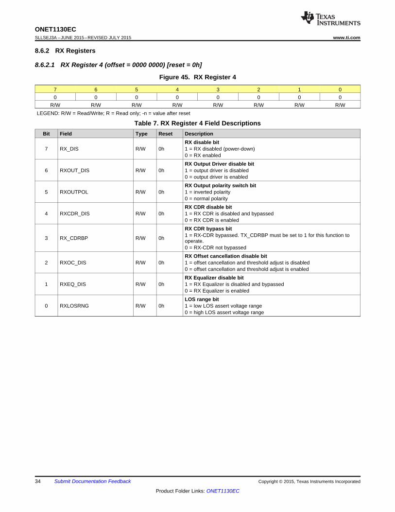
ONET1130ECSLLSEJ3A –JUNE 2015–REVISED JULY 2015 www.ti.com
8.6.2 RX Registers
8.6.2.1 RX Register 4 (offset = 0000 0000) [reset = 0h]
Figure 45. RX Register 4
7 6 5 4 3 2 1 00 0 0 0 0 0 0 0
R/W R/W R/W R/W R/W R/W R/W R/WLEGEND: R/W = Read/Write; R = Read only; -n = value after reset
Table 7. RX Register 4 Field DescriptionsBit Field Type Reset Description
RX disable bit7 RX_DIS R/W 0h 1 = RX disabled (power-down)
0 = RX enabledRX Output Driver disable bit
6 RXOUT_DIS R/W 0h 1 = output driver is disabled0 = output driver is enabledRX Output polarity switch bit
5 RXOUTPOL R/W 0h 1 = inverted polarity0 = normal polarityRX CDR disable bit
4 RXCDR_DIS R/W 0h 1 = RX CDR is disabled and bypassed0 = RX CDR is enabledRX CDR bypass bit1 = RX-CDR bypassed. TX_CDRBP must be set to 1 for this function to3 RX_CDRBP R/W 0h operate.0 = RX-CDR not bypassedRX Offset cancellation disable bit
2 RXOC_DIS R/W 0h 1 = offset cancellation and threshold adjust is disabled0 = offset cancellation and threshold adjust is enabledRX Equalizer disable bit
1 RXEQ_DIS R/W 0h 1 = RX Equalizer is disabled and bypassed0 = RX Equalizer is enabledLOS range bit
0 RXLOSRNG R/W 0h 1 = low LOS assert voltage range0 = high LOS assert voltage range
34 Submit Documentation Feedback Copyright © 2015, Texas Instruments Incorporated
Product Folder Links: ONET1130EC

ONET1130ECwww.ti.com SLLSEJ3A –JUNE 2015–REVISED JULY 2015
8.6.2.2 RX Register 5 (offset = 0000 0000) [reset = 0h]
Figure 46. RX Register 5
7 6 5 4 3 2 1 0Reserved 0 0 0 0
R/W R/W R/W R/W R/W R/W R/W R/WLEGEND: R/W = Read/Write; R = Read only; -n = value after reset
Table 8. RX Register 5 Field DescriptionsBit Field Type Reset Description7:4 – R/W 0h Reserved
Receiver fast LOS bit3 RXFLOS R/W 0h 1 = Fast LOS
0 = normal operation2 RXCTLE2 R/W 0h RX input CTLE setting
000 = minimum1 RXCTLE1 R/W 0h111 = maximum
0 RXCTLE0 R/W 0h
8.6.2.3 RX Register 6 (offset = 0000 0000) [reset = 0h]
Figure 47. RX Register 6
7 6 5 4 3 2 1 00 Reserved 0 0 0 0 0
R/W R/W R/W R/W R/W R/W R/W R/WLEGEND: R/W = Read/Write; R = Read only; -n = value after reset
Table 9. RX Register 6 Field DescriptionsBit Field Type Reset Description
Receiver Hysteresis7 RXHYS R/W 0h 1 = Reduce hysteresis level by approximately 2dB
0 = default level of hysteresis (approximately 4dB)6:5 – R/W 0h Reserved4 RXTHSGN R/W 0h RX Eye cross-point adjustment setting
RXTHSGN = 1 (positive shift)3 RXTHADJ3 R/W 0hMaximum shift for 11112 RXTHADJ2 R/W 0hMinimum shift for 00001 RXTHADJ1 R/W 0h
RXTHSGN = 0 (negative shift)
Maximum shift for 11110 RXTHADJ0 R/W 0hMinimum shift for 0000
Copyright © 2015, Texas Instruments Incorporated Submit Documentation Feedback 35
Product Folder Links: ONET1130EC

ONET1130ECSLLSEJ3A –JUNE 2015–REVISED JULY 2015 www.ti.com
8.6.2.4 RX Register 7 (offset = 0000 0000) [reset = 0h]
Figure 48. RX Register 7
7 6 5 4 3 2 1 0Reserved 0 0 0 0 0 0
R/W R/W R/W R/W R/W R/W R/W R/WLEGEND: R/W = Read/Write; R = Read only; -n = value after reset
Table 10. RX Register 7 Field DescriptionsBit Field Type Reset Description7:6 – R/W 0h Reserved5 RXLOSA5 R/W 0h LOS assert level
Minimum LOS assert level for 0000004 RXLOSA4 R/W 0hMaximum LOS assert level for 111111
3 RXLOSA3 R/W 0h2 RXLOSA2 R/W 0h1 RXLOSA1 R/W 0h0 RXLOSA0 R/W 0h
8.6.2.5 RX Register 8 (offset = 0000 0000) [reset = 0h]
Figure 49. RX Register 8
7 6 5 4 3 2 1 0Reserved 0 0 0 0 0 0 0
R/W R/W R/W R/W R/W R/W R/W R/WLEGEND: R/W = Read/Write; R = Read only; -n = value after reset
Table 11. RX Register 8 Field DescriptionsBit Field Type Reset Description7 – R/W 0h Reserved6 RXDADJ1 R/W 0h RX output de-emphasis setting
00 = minimum de-emphasis5 RXDADJ0 R/W 0h 11 = maximum de-emphasis
RX driver short circuit protection4 RXDRVSC R/W 0h 1 = short circuit protection enabled
0 = normal operation3 RXAMP3 R/W 0h RX output amplitude adjustment
0000 = minimum amplitude2 RXAMP2 R/W 0h1111 = maximum amplitude
1 RXAMP1 R/W 0h0 RXAMP0 R/W 0h
36 Submit Documentation Feedback Copyright © 2015, Texas Instruments Incorporated
Product Folder Links: ONET1130EC

ONET1130ECwww.ti.com SLLSEJ3A –JUNE 2015–REVISED JULY 2015
8.6.2.6 RX Register 9 (offset = 0000 0000) [reset = 0h]
Figure 50. RX Register 9
7 6 5 4 3 2 1 00 0 0 0 0 0 0 0
R/W R/W R/W R/W R/W R/W R/W R/WLEGEND: R/W = Read/Write; R = Read only; -n = value after reset
Table 12. RX Register 9 Field DescriptionsBit Field Type Reset Description7 RXFD_MOD1 R/W 0h RX frequency detection mode selection
00 = auto selection enabled01 = Pre-selected to 10.3Gbps
6 RXFD_MOD0 R/W 0h 10 = Pre-select to 11.1Gbps11 = test mode (do not use)RX frequency detector enable bit
5 RXFD_EN R/W 0h 1 = RX frequency detector is always enabled0 = RX frequency detector in automatic modeRX frequency detector disable bit
4 RXFD_DIS R/W 0h 1 = RX frequency detector is always disabled0 = RX frequency detector is in automatic modeRX CDR fast lock disable bit
3 RXFL_DIS R/W 0h 1 = RX CDR fast lock disabled0 = RX CDR in fast lock mode
2 RXDIV2 R/W 0h RX Divider Ratio000: Full-Rate,1 RXDIV1 R/W 0h001: Divide by 2010: Divide by 4011: Divide by 80 RXDIV0 R/W 0h100: Divide by 16101: Divide by 32
Copyright © 2015, Texas Instruments Incorporated Submit Documentation Feedback 37
Product Folder Links: ONET1130EC

ONET1130ECSLLSEJ3A –JUNE 2015–REVISED JULY 2015 www.ti.com
8.6.3 TX Registers
8.6.3.1 TX Register 10 (offset = 0000 0000) [reset = 0h]
Figure 51. TX Register 10
7 6 5 4 3 2 1 00 0 0 0 0 0 0 0
R/W R/W R/W R/W R/W R/W R/W R/WLEGEND: R/W = Read/Write; R = Read only; -n = value after reset
Table 13. TX Register 10 Field DescriptionsBit Field Type Reset Description
TX disable bit7 TX_DIS R/W 0h 1 = TX disabled (power-down)
0 = TX enabledTX Output Driver disable bit
6 TXOUT_DIS R/W 0h 1 = output disabled0 = output enabledTX Output polarity switch bit
5 TXOUTPOL R/W 0h 1 = inverted polarity0 = normal polarityTX CDR disable bit
4 TXCDR_DIS R/W 0h 1 = TX CDR is disabled and bypassed0 = TX CDR is enabledTX CDR bypass bit1 = TX-CDR bypassed. RX_CDRBP must be set to 1 for this function to3 TX_CDRBP R/W 0h operate.0 = TX-CDR not bypassedTX OC disable bit
2 TXOC_DIS R/W 0h 1 = TX Offset Cancellation disabled0 = TX Offset Cancellation enabledTX Equalizer disable bit
1 TXEQ_DIS R/W 0h 1 = TX Equalizer is disabled and bypassed0 = TX Equalizer is enabledTX AMP Ctrl
0 TXAMPCTRL R/W 0h 1 = TX AMP Control is enabled (analog amplitude control)0 = TX AMP Control is disabled (digital amplitude control)
38 Submit Documentation Feedback Copyright © 2015, Texas Instruments Incorporated
Product Folder Links: ONET1130EC
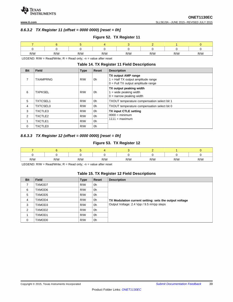
ONET1130ECwww.ti.com SLLSEJ3A –JUNE 2015–REVISED JULY 2015
8.6.3.2 TX Register 11 (offset = 0000 0000) [reset = 0h]
Figure 52. TX Register 11
7 6 5 4 3 2 1 00 0 0 0 0 0 0 0
R/W R/W R/W R/W R/W R/W R/W R/WLEGEND: R/W = Read/Write; R = Read only; -n = value after reset
Table 14. TX Register 11 Field DescriptionsBit Field Type Reset Description
TX output AMP range7 TXAMPRNG R/W 0h 1 = Half TX output amplitude range
0 = Full TX output amplitude rangeTX output peaking width
6 TXPKSEL R/W 0h 1 = wide peaking width0 = narrow peaking width
5 TXTCSEL1 R/W 0h TXOUT temperature compensation select bit 14 TXTCSEL0 R/W 0h TXOUT temperature compensation select bit 03 TXCTLE3 R/W 0h TX input CTLE setting
0000 = minimum2 TXCTLE2 R/W 0h1111 = maximum
1 TXCTLE1 R/W 0h0 TXCTLE0 R/W 0h
8.6.3.3 TX Register 12 (offset = 0000 0000) [reset = 0h]
Figure 53. TX Register 12
7 6 5 4 3 2 1 00 0 0 0 0 0 0 0
R/W R/W R/W R/W R/W R/W R/W R/WLEGEND: R/W = Read/Write; R = Read only; -n = value after reset
Table 15. TX Register 12 Field DescriptionsBit Field Type Reset Description7 TXMOD7 R/W 0h6 TXMOD6 R/W 0h5 TXMOD5 R/W 0h4 TXMOD4 R/W 0h TX Modulation current setting: sets the output voltage
Output Voltage: 2.4 Vpp / 9.5 mVpp steps3 TXMOD3 R/W 0h2 TXMOD2 R/W 0h1 TXMOD1 R/W 0h0 TXMOD0 R/W 0h
Copyright © 2015, Texas Instruments Incorporated Submit Documentation Feedback 39
Product Folder Links: ONET1130EC

ONET1130ECSLLSEJ3A –JUNE 2015–REVISED JULY 2015 www.ti.com
8.6.3.4 TX Register 13 (offset = 0h) [reset = 0]
Figure 54. TX Register 13
7 6 5 4 3 2 1 00 0 0 0 0 0 0 0
R/W R/W R/W R/W R/W R/W R/W R/WLEGEND: R/W = Read/Write; R = Read only; -n = value after reset
Table 16. TX Register 13 Field DescriptionsBit Field Type Reset Description
TX output selection bit7 TXOUTSEL R/W 0h 1 = The negative output TXOUT– is active if TXMODE = 1
0 = The positive output TXOUT+ is active if TXMODE = 1TX output mode selection bit
6 TXMODE R/W 0h 1 = Single-ended mode0 = Differential modeTX output de-emphasis mode selection bit
5 TXSTEP R/W 0h 1 = Delayed de-emphasis0 = Normal de-emphasisTX edge speed selection bit
4 TXSLOW R/W 0h 1 = Slow edge speed0 = Normal operation
3 TXDEADJ3 R/W 0h TX de-emphasis setting0000 = minimum2 TXDEADJ2 R/W 0h1111 = maximum
1 TXDEADJ1 R/W 0h0 TXDEADJ0 R/W 0h
8.6.3.5 TX Register 14 (offset = 0000 0000) [reset = 0h]
Figure 55. TX Register 14
7 6 5 4 3 2 1 00 0 0 0 0 0 0 0
R/W R/W R/W R/W R/W R/W R/W R/WLEGEND: R/W = Read/Write; R = Read only; -n = value after reset
Table 17. TX Register 14 Field DescriptionsBit Field Type Reset Description7 TXCPSGN R/W 0h TX Eye cross-point adjustment setting
TXCPSGN = 1 (positive shift)6 TXCPADJ6 R/W 0hMaximum shift for 11111115 TXCPADJ5 R/W 0hMinimum shift for 00000004 TXCPADJ4 R/W 0h
TXCPSGN = 0 (negative shift)3 TXCPADJ3 R/W 0h
Maximum shift for 11111112 TXCPADJ2 R/W 0h
Minimum shift for 00000001 TXCPADJ1 R/W 0h0 TXCPADJ0 R/W 0h
40 Submit Documentation Feedback Copyright © 2015, Texas Instruments Incorporated
Product Folder Links: ONET1130EC

ONET1130ECwww.ti.com SLLSEJ3A –JUNE 2015–REVISED JULY 2015
8.6.3.6 TX Register 15 (offset = 0000 0000) [reset = 0h]
Figure 56. TX Register 15
7 6 5 4 3 2 1 00 0 0 0 0 0 0 0
R/W R/W R/W R/W R/W R/W R/W R/WLEGEND: R/W = Read/Write; R = Read only; -n = value after reset
Table 18. TX Register 15 Field DescriptionsBit Field Type Reset Description7 TXBIAS9 R/W 0h Bias current settings (8MSB; 2LSBs are in register 16)
Closed loop (APC):6 TXBIAS8 R/W 0hCoupling ratio CR = IBIAS / IPD, TXBIAS = 0..1023, IBIAS ≤ 150mA:
5 TXBIAS7 R/W 0 h TXPDRNG = 00; IBIAS = 0.75μA x CR x TXBIAS4 TXBIAS6 R/W 0h TXPDRNG = 01; IBIAS = 1.5μA x CR x TXBIAS
TXPDRNG = 1X; IBIAS = 3μA x CR x TXBIAS3 TXBIAS5 R/W 0hOpen Loop:2 TXBIAS4 R/W 0hIBIAS ~ 156μA x TXBIAS in source mode
1 TXBIAS3 R/W 0h IBIAS ~ 156μA x TXBIAS in sink mode0 TXBIAS2 R/W 0h
8.6.3.7 TX Register 16 (offset = 0000 0000) [reset = 0h]
Figure 57. TX Register 16
7 6 5 4 3 2 1 0Reserved 0 0 Reserved 0 0
R/W R/W R/W R/W R/W R/W R/W R/WLEGEND: R/W = Read/Write; R = Read only; -n = value after reset
Table 19. TX Register 16 Field DescriptionsBit Field Type Reset Description7 – R/W 0h Reserved
Digital photodiode current monitor selection bit (MONP)6 TXDMONP R/W 0h 1 = Digital photodiode monitor is active (no external resistor is needed)
0 = Analog photodiode monitor is active (external resistor is required)Digital bias current monitor selection bit (MONB)
5 TXDMONB R/W 0h 1 = Digital bias current monitor is active (no external resistor is needed)0 = Analog bias current monitor is active (external resistor is required)
4:2 – R/W 0h Reserved1 TXBIAS1 R/W 0h
Bias current setting (2 LSBs)0 TXBIAS0 R/W 0h
Copyright © 2015, Texas Instruments Incorporated Submit Documentation Feedback 41
Product Folder Links: ONET1130EC

ONET1130ECSLLSEJ3A –JUNE 2015–REVISED JULY 2015 www.ti.com
8.6.3.8 TX Register 17 (offset = 0000 0000) [reset = 0h]
Figure 58. TX Register 17
7 6 5 4 3 2 1 00 0 0 0 0 0 0 0
R/W R/W R/W R/W R/W R/W R/W R/WLEGEND: R/W = Read/Write; R = Read only; -n = value after reset
Table 20. TX Register 17 Field DescriptionsBit Field Type Reset Description7 TXBMF7 R/W 0h Bias current monitor fault threshold
With TXDMONB = 16 TXBMF6 R/W 0h Register sets the value of the bias current that will trigger a fault.5 TXBMF5 R/W 0h The external resistor on the MONB pin must be removed to use this
feature.4 TXBMF4 R/W 0h3 TXBMF3 R/W 0h2 TXBMF2 R/W 0h1 TXBMF1 R/W 0h0 TXBMF0 R/W 0h
8.6.3.9 TX Register 18 (offset = 0000 0000) [reset = 0h]
Figure 59. TX Register 18
7 6 5 4 3 2 1 00 0 0 0 0 0 0 0
R/W R/W R/W R/W R/W R/W R/W R/WLEGEND: R/W = Read/Write; R = Read only; -n = value after reset
Table 21. TX Register 18 Field DescriptionsBit Field Type Reset Description7 TXPMF7 R/W 0h Power monitor fault threshold
With TXDMONP = 16 TXPMF6 R/W 0h Register sets the value of the photodiode current that will trigger a fault.5 TXPMF5 R/W 0h The external resistor on the MONP pin must be removed to use this
feature.4 TXPMF4 R/W 0h3 TXPMF3 R/W 0h2 TXPMF2 R/W 0h1 TXPMF1 R/W 0h0 TXPMF0 R/W 0h
42 Submit Documentation Feedback Copyright © 2015, Texas Instruments Incorporated
Product Folder Links: ONET1130EC

ONET1130ECwww.ti.com SLLSEJ3A –JUNE 2015–REVISED JULY 2015
8.6.3.10 TX Register 19 (offset = 0000 0000) [reset = 0h]
Figure 60. TX Register 19
7 6 5 4 3 2 1 00 0 0 0 0 0 0 0
R/W R/W R/W R/W R/W R/W R/W R/WLEGEND: R/W = Read/Write; R = Read only; -n = value after reset
Table 22. TX Register 19 Field DescriptionsBit Field Type Reset Description7 TXFD_MOD1 R/W 0 TX frequency detection mode selection
00 = auto selection enabled01 = Pre-selected to 10.3Gbps
6 TXFD_MOD0 R/W 0 10 = Pre-select to 11.1Gbps11 = test mode (do not use)TX frequency detector enable bit
5 TXFD_EN R/W 0 1 =TX frequency detector is always enabled0 = TX frequency detector in automatic modeTX frequency detector disable bit
4 TXFD_DIS R/W 0 1 = TX frequency detector is always disabled0 = TX frequency detector is in automatic modeTX CDR fast lock disable bit
3 TXFL_DIS R/W 0 1 = TX CDR fast lock disabled0 = TX CDR in fast lock mode
2 TXDIV2 R/W 0 TX Divider Ratio000: Full-Rate,1 TXDIV1 R/W 0001: Divide by 2010: Divide by 4011: Divide by 80 TXDIV0 R/W 0100: Divide by 16101: Divide by 32
Copyright © 2015, Texas Instruments Incorporated Submit Documentation Feedback 43
Product Folder Links: ONET1130EC

ONET1130ECSLLSEJ3A –JUNE 2015–REVISED JULY 2015 www.ti.com
8.6.4 Reserved Registers
8.6.4.1 Reserved Registers 20-39
Figure 61. Reserved Registers 20-39
7 6 5 4 3 2 1 0Reserved
R/W R/W R/W R/W R/W R/W R/W R/WLEGEND: R/W = Read/Write; R = Read only; -n = value after reset
Table 23. Reserved Registers 20-39 Field DescriptionsBit Field Type Reset Description7:0 – – – Reserved
44 Submit Documentation Feedback Copyright © 2015, Texas Instruments Incorporated
Product Folder Links: ONET1130EC

ONET1130ECwww.ti.com SLLSEJ3A –JUNE 2015–REVISED JULY 2015
8.6.5 Read Only Registers
8.6.5.1 Core Level Register 40 (offset = 0000 0000) [reset = 0h]
Figure 62. Core Level Register 40
7 6 5 4 3 2 1 00 0 0 0 0 0 0 0R R R R R R R R
LEGEND: R/W = Read/Write; R = Read only; -n = value after reset
Table 24. Core Level Register 40 Field DescriptionsBit Field Type Reset Description7 ADC9 (MSB) R 0h Digital representation of the ADC input source (read only)6 ADC8 R 0h5 ADC7 R 0h4 ADC6 R 0h3 ADC5 R 0h2 ADC4 R 0h1 ADC3 R 0h0 ADC2 R 0h
8.6.5.2 Core Level Register 41 (offset = 0000 0000) [reset = 0h]
Figure 63. Core Level Register 41
7 6 5 4 3 2 1 0Reserved 0 0
R R R R R R R RLEGEND: R/W = Read/Write; R = Read only; -n = value after reset
Table 25. Core Level Register 41 Field DescriptionsBit Field Type Reset Description7:2 – R 0h Reserved1 ADC1 R 0h Digital representation of the ADC input source (read only)0 ADC0 (LSB) R 0h
Copyright © 2015, Texas Instruments Incorporated Submit Documentation Feedback 45
Product Folder Links: ONET1130EC

ONET1130ECSLLSEJ3A –JUNE 2015–REVISED JULY 2015 www.ti.com
8.6.5.3 RX Registers 42 (offset = 0000 0000) [reset = 0h]
Figure 64. RX Registers 42
7 6 5 4 3 2 1 00 0 0 0 ReservedR R R R R R R R
LEGEND: R/W = Read/Write; R = Read only; -n = value after reset; RCLR = Read clear
Table 26. RX Registers 42 Field DescriptionsBit Field Type Reset Description
RX CDR lock status bit7 RXCDRLock R 0 1 = RX CDR is not locked
0 = RX CDR is lockedLatched low status of bit 7. Cleared when read.
6 RXCDRlock (latched LOW) RCLR 0 Latched low bit set to 0 when raw status goes low and keep it low even ifraw status goes high.RX LOS status bit
5 RXLOS R 0 1 = RX LOS asserted0 = RX LOS de-assertedLatched high status of RXLOS(bit5). Cleared when read.
4 RX_LOS (latched high) RCLR 0 Latched high status set to 1 when raw status goes high and keep it higheven if raw status goes low.
3:0 – R 0 Reserved
46 Submit Documentation Feedback Copyright © 2015, Texas Instruments Incorporated
Product Folder Links: ONET1130EC

ONET1130ECwww.ti.com SLLSEJ3A –JUNE 2015–REVISED JULY 2015
8.6.5.4 TX Register 43 (offset = 0000 0000) [reset = 0h]
Figure 65. Core Level Register 43
7 6 5 4 3 2 1 00 0 0 0 ReservedR R R R R R R R
LEGEND: R/W = Read/Write; R = Read only; -n = value after reset; RCLR = Read clear
Table 27. TX Registers 43 Field DescriptionsBit Field Type Reset Description
TX CDR lock status bit7 TXCDRLock R 0 1 = TX CDR is not locked
0 = TX CDR is lockedLatched low status of bit 7. Cleared when read.
6 TXCDRLock (latched Low) RCLR 0 Latched low bit set to 0 when raw status goes low and keep it low even ifraw status goes high.TX fault status bit
5 TX_FLT R 0 1 = TX fault detected0 = TX fault not detectedTX driver disable status bit
4 TX_DRVDIS R 0 1 = TX fault logic disables the driver0 = TX fault logic does not disable the driver
3:0 – R 0 Reserved
Copyright © 2015, Texas Instruments Incorporated Submit Documentation Feedback 47
Product Folder Links: ONET1130EC

ONET1130ECSLLSEJ3A –JUNE 2015–REVISED JULY 2015 www.ti.com
8.6.6 Adjustment Registers
8.6.6.1 Adjustment Registers 44-50
Figure 66. Adjustment Registers 44-50
7 6 5 4 3 2 1 0Reserved
R R R R R R R RLEGEND: R/W = Read/Write; R = Read only; -n = value after reset
Table 28. Adjustment Registers 44-50 Field DescriptionsBit Field Type Reset Description7:0 – – – Reserved
8.6.6.2 Adjustment Register 51 (offset = 0100 0000) [reset = 40h]
Figure 67. Adjustment Register 51
7 6 5 4 3 2 1 00 1 0 ReservedR R R R R R R R
LEGEND: R/W = Read/Write; R = Read only; -n = value after reset
Table 29. Adjustment Register 51 Field DescriptionsBit Field Type Reset Description7 SEL_RES_2 R/W 0 TX and RX CDR Loop Filter Resistor
000: 75,6 SEL_RES_1 R/W 1001: 150010: 225011: 300100: 375
5 SEL_RES_0 R/W 0 101: 450110: 525111: 600Default = 225
4:0 – R/W 0 Reserved
48 Submit Documentation Feedback Copyright © 2015, Texas Instruments Incorporated
Product Folder Links: ONET1130EC

VC
C_T
X
TXIN+
TXIN-
TX
_LF
GND
RXIN+
SDA
RX
_LF
VC
C_R
X
RX
OU
T+
VC
C_R
X
RX_LOS
RXIN-
GND
SCK
GND
LOL
GND
PD
RX
OU
T-
VD
D
VC
C_T
X
TX
OU
T+
TX
OU
T-
ONET1130ECTXIN+
TXIN-
0.1�F
0.1�F
LOL
TX_DIS
0.1�F
VCC_TX0.1�F
RXIN+
RXIN-
0.1�F
SDA
SCK
BIA
S
0.1�F
VCC_RX
RXOUT-
RXOUT+
0.1�F
0.1�F
MONP
0.1�F 0.1�F
2.2nF
2.2nF
MONB
MONP
AM
P
COMP
TX
_DIS
TX
_FLT
RX
_DIS
MONB
TX_FLT
VDD
LOS0.01�F
4.7k to10k
VCC_R
4.7k to10k
VCC_T
4.7k to10k
MZ MOD+
MZ MOD-
0.1�F 0.1�F
VCC
4.7k to10k
VCC
4.7k to10k
4.7k to10k
ONET1130ECwww.ti.com SLLSEJ3A –JUNE 2015–REVISED JULY 2015
9 Application Information and Implementations
NOTEInformation in the following applications sections is not part of the TI componentspecification, and TI does not warrant its accuracy or completeness. TI’s customers areresponsible for determining suitability of components for their purposes. Customers shouldvalidate and test their design implementation to confirm system functionality.
9.1 Application InformationThe ONET1130EC is designed to be used in conjunction with a Transmitter Optical Sub-Assembly (TOSA) and aReceiver Optical Sub-Assembly (ROSA). The ONET1130EC, TOSA, ROSA, microcontroller and powermanagement circuitry will typically be used in an XFP or SFP+ 10 Gbps optical transceiver. Figure 68 shows theONET1130EC in differential mode of operation modulating a differentially driven Mach Zehnder (MZ) modulatorTOSA and Figure 70 and Figure 71 show the device in single-ended output mode with an ElectroabsorptiveModulated Laser (EML) TOSA. Figure 70 has the photodiode cathode available and Figure 71 has thephotodiode anode available.
9.2 Typical Application, Transmitter Differential Mode
Figure 68. Typical Application Circuit in Differential Mode
Copyright © 2015, Texas Instruments Incorporated Submit Documentation Feedback 49
Product Folder Links: ONET1130EC

ONET1130ECSLLSEJ3A –JUNE 2015–REVISED JULY 2015 www.ti.com
Typical Application, Transmitter Differential Mode (continued)9.2.1 Design Requirements
Table 30. Design ParametersPARAMETER VALUESupply voltage 2.5 VTransmitter input voltage 100 mVpp to 1000 mVpp differentialTransmitter output voltage 1 Vpp to 3.6 Vpp differentialReceiver input voltage 6 mVpp to 800 mVpp differentialReceiver output voltage 300 mVpp to 900 mVpp differential
9.2.2 Detailed Design ProcedureIn the transmitter differential mode of operation, the output driver is intended to be used with a differentiallydriven Mach Zehnder (MZ) modulator TOSA. On the input side, the TXIN+ and TXIN- pins are required to be ACcoupled to the signal from the host system and the input voltage should be between 100 mVpp and 1000 mVppdifferential. On the output side, the TXOUT+ pin is AC coupled to the modulator positive input and the TXOUT–pin is AC coupled to the modulator negative input. A bias-T from VCC to both the TXOUT+ and TXOUT– pins isrequired to supply sufficient headroom voltage for the output driver transistors. It is recommended that theinductance in the bias-T have low DC resistance to limit the DC voltage drop and maximize the voltage suppliedto the TXOUT+ and TXOUT– pins. If the voltage on these pins drops below approximately 2.1V then the outputrise and fall times can be adversely affected.
The receiver inputs, RXIN+ and RXIN–, are AC coupled to the output of ROSA and the input voltage should bebetween 6 mVpp and 800 mVpp differential. The receiver outputs, RXOUT+ and RXOUT–, are AC coupled to thereceiver input of the host system.
9.2.3 Application Curve
Figure 69. Differential Mode Transmitter Output Eye Diagram
50 Submit Documentation Feedback Copyright © 2015, Texas Instruments Incorporated
Product Folder Links: ONET1130EC
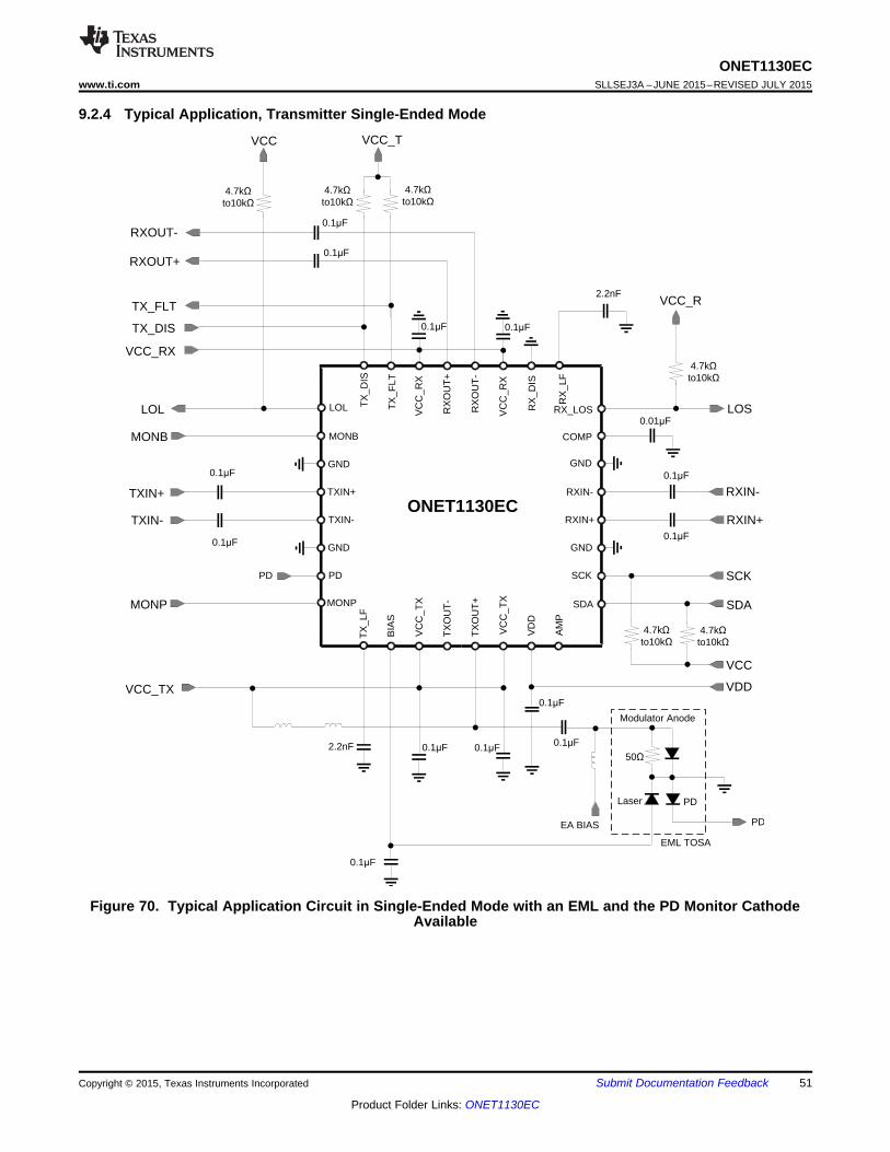
VC
C_T
X
TXIN+
TXIN-
TX
_LF
GND
RXIN+
SDA
RX
_LF
VC
C_R
X
RX
OU
T+
VC
C_R
XRX_LOS
RXIN-
GND
SCK
GND
LOL
GND
PD
RX
OU
T-
VD
D
VC
C_T
X
TX
OU
T+
TX
OU
T-
ONET1130ECTXIN+
TXIN-
0.1�F
0.1�F
LOL
TX_DIS
0.1�F
Laser
VCC_TX
0.1�F 0.1�F
Modulator Anode
EA BIAS
50
PD
EML TOSA
0.1�F
RXIN+
RXIN-
0.1�F
SDA
SCK
BIA
S
0.1�F
VCC_RX
RXOUT-
RXOUT+
0.1�F
0.1�F
MONP
0.1�F 0.1�F
PD
2.2nF
2.2nF
MONB
MONP
AM
P
COMP
TX
_DIS
TX
_FLT
RX
_DIS
MONB
TX_FLT
VDD
LOS0.01�F
0.1�F
PD
4.7k to10k
VCC_R
4.7k to10k
VCC_T
4.7k to10k
VCC
4.7k to10k
VCC
4.7k to10k
4.7k to10k
ONET1130ECwww.ti.com SLLSEJ3A –JUNE 2015–REVISED JULY 2015
9.2.4 Typical Application, Transmitter Single-Ended Mode
Figure 70. Typical Application Circuit in Single-Ended Mode with an EML and the PD Monitor CathodeAvailable
Copyright © 2015, Texas Instruments Incorporated Submit Documentation Feedback 51
Product Folder Links: ONET1130EC

VC
C_T
X
TXIN+
TXIN-
TX
_LF
GND
RXIN+
SDA
RX
_LF
VC
C_R
X
RX
OU
T+
VC
C_R
X
RX_LOS
RXIN-
GND
SCK
GND
LOL
GND
PD
RX
OU
T-
VD
D
VC
C_T
X
TX
OU
T+
TX
OU
T-
ONET1130ECTXIN+
TXIN-
0.1�F
0.1�F
LOL
TX_DIS
0.1�F
Laser
VCC_TX
0.1�F 0.1�F
Modulator Anode
EA BIAS
50
PD
EML TOSA
0.1�F
RXIN+
RXIN-
0.1�F
SDA
SCK
BIA
S
0.1�F
VCC_RX
RXOUT-
RXOUT+
0.1�F
0.1�F
MONP
0.1�F 0.1�F
PD
2.2nF
2.2nF
MONB
MONP
AM
P
COMP
TX
_DIS
TX
_FLT
RX
_DIS
MONB
TX_FLT
VDD
LOS
4.7k �to 10k
0.01�F
0.1�F
PD
VCC_R
-3V
4.7k to 10k
4.7k to 10k
VCC_T
4.7k to10k
VCC
VCC
4.7k to10k
4.7k to10k
ONET1130ECSLLSEJ3A –JUNE 2015–REVISED JULY 2015 www.ti.com
Figure 71. Typical Application Circuit in Single-Ended Mode with an EML and the PD Monitor AnodeAvailable
52 Submit Documentation Feedback Copyright © 2015, Texas Instruments Incorporated
Product Folder Links: ONET1130EC
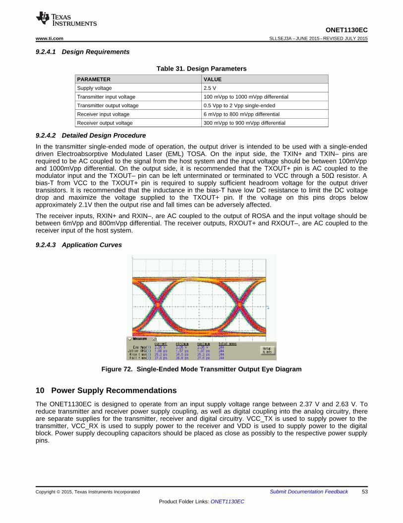
ONET1130ECwww.ti.com SLLSEJ3A –JUNE 2015–REVISED JULY 2015
9.2.4.1 Design Requirements
Table 31. Design ParametersPARAMETER VALUESupply voltage 2.5 VTransmitter input voltage 100 mVpp to 1000 mVpp differentialTransmitter output voltage 0.5 Vpp to 2 Vpp single-endedReceiver input voltage 6 mVpp to 800 mVpp differentialReceiver output voltage 300 mVpp to 900 mVpp differential
9.2.4.2 Detailed Design ProcedureIn the transmitter single-ended mode of operation, the output driver is intended to be used with a single-endeddriven Electroabsorptive Modulated Laser (EML) TOSA. On the input side, the TXIN+ and TXIN– pins arerequired to be AC coupled to the signal from the host system and the input voltage should be between 100mVppand 1000mVpp differential. On the output side, it is recommended that the TXOUT+ pin is AC coupled to themodulator input and the TXOUT– pin can be left unterminated or terminated to VCC through a 50Ω resistor. Abias-T from VCC to the TXOUT+ pin is required to supply sufficient headroom voltage for the output drivertransistors. It is recommended that the inductance in the bias-T have low DC resistance to limit the DC voltagedrop and maximize the voltage supplied to the TXOUT+ pin. If the voltage on this pins drops belowapproximately 2.1V then the output rise and fall times can be adversely affected.
The receiver inputs, RXIN+ and RXIN–, are AC coupled to the output of ROSA and the input voltage should bebetween 6mVpp and 800mVpp differential. The receiver outputs, RXOUT+ and RXOUT–, are AC coupled to thereceiver input of the host system.
9.2.4.3 Application Curves
Figure 72. Single-Ended Mode Transmitter Output Eye Diagram
10 Power Supply RecommendationsThe ONET1130EC is designed to operate from an input supply voltage range between 2.37 V and 2.63 V. Toreduce transmitter and receiver power supply coupling, as well as digital coupling into the analog circuitry, thereare separate supplies for the transmitter, receiver and digital circuitry. VCC_TX is used to supply power to thetransmitter, VCC_RX is used to supply power to the receiver and VDD is used to supply power to the digitalblock. Power supply decoupling capacitors should be placed as close as possibly to the respective power supplypins.
Copyright © 2015, Texas Instruments Incorporated Submit Documentation Feedback 53
Product Folder Links: ONET1130EC

TX
OU
T+
TXOUT-
TXIN+
TXIN-
RXIN-
RXIN+
RX
OU
T-
RX
OU
T+
From
ROSA
To
TO
SA
From
Host
To
Ho
st
AC-coupling
capacitors
50O��to VCC
Termination
Bias-T
Ferrites
ONET1130ECSLLSEJ3A –JUNE 2015–REVISED JULY 2015 www.ti.com
11 Layout
11.1 Layout GuidelinesFor optimum performance, use 50-Ω transmission lines (100-Ω differential) for connecting the high speed inputsand outputs. The length of transmission lines should be kept as short as possible to reduce loss and pattern-dependent jitter. It is recommended to maximize the separation of the TXOUT+ and TXOUT- transmission linesfrom the RXIN+ and RXIN- transmission lines to minimize transmitter to receiver crosstalk.
If the single-ended mode of operation is being used (TXMODE = 1) then it is recommended to terminate theunused output with a 50-Ω resistor to VCC. Figure 73 shows a typical layout for the high speed inputs andoutputs.
11.2 Layout Example
Figure 73. Board Layout
54 Submit Documentation Feedback Copyright © 2015, Texas Instruments Incorporated
Product Folder Links: ONET1130EC

ONET1130ECwww.ti.com SLLSEJ3A –JUNE 2015–REVISED JULY 2015
12 Device and Documentation Support
12.1 Community ResourcesThe following links connect to TI community resources. Linked contents are provided "AS IS" by the respectivecontributors. They do not constitute TI specifications and do not necessarily reflect TI's views; see TI's Terms ofUse.
TI E2E™ Online Community TI's Engineer-to-Engineer (E2E) Community. Created to foster collaborationamong engineers. At e2e.ti.com, you can ask questions, share knowledge, explore ideas and helpsolve problems with fellow engineers.
Design Support TI's Design Support Quickly find helpful E2E forums along with design support tools andcontact information for technical support.
12.2 TrademarksE2E is a trademark of Texas Instruments.All other trademarks are the property of their respective owners.
12.3 Electrostatic Discharge CautionThese devices have limited built-in ESD protection. The leads should be shorted together or the device placed in conductive foamduring storage or handling to prevent electrostatic damage to the MOS gates.
12.4 GlossarySLYZ022 — TI Glossary.
This glossary lists and explains terms, acronyms, and definitions.
13 Mechanical, Packaging, and Orderable InformationThe following pages include mechanical, packaging, and orderable information. This information is the mostcurrent data available for the designated devices. This data is subject to change without notice and revision ofthis document. For browser-based versions of this data sheet, refer to the left-hand navigation.
Copyright © 2015, Texas Instruments Incorporated Submit Documentation Feedback 55
Product Folder Links: ONET1130EC
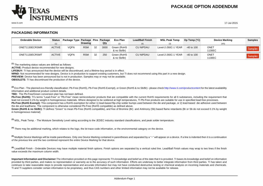
PACKAGE OPTION ADDENDUM
www.ti.com 17-Jul-2015
Addendum-Page 1
PACKAGING INFORMATION
Orderable Device Status(1)
Package Type PackageDrawing
Pins PackageQty
Eco Plan(2)
Lead/Ball Finish(6)
MSL Peak Temp(3)
Op Temp (°C) Device Marking(4/5)
Samples
ONET1130ECRSMR ACTIVE VQFN RSM 32 3000 Green (RoHS& no Sb/Br)
CU NIPDAU Level-2-260C-1 YEAR -40 to 100 ONET1130EC
ONET1130ECRSMT ACTIVE VQFN RSM 32 250 Green (RoHS& no Sb/Br)
CU NIPDAU Level-2-260C-1 YEAR -40 to 100 ONET1130EC
(1) The marketing status values are defined as follows:ACTIVE: Product device recommended for new designs.LIFEBUY: TI has announced that the device will be discontinued, and a lifetime-buy period is in effect.NRND: Not recommended for new designs. Device is in production to support existing customers, but TI does not recommend using this part in a new design.PREVIEW: Device has been announced but is not in production. Samples may or may not be available.OBSOLETE: TI has discontinued the production of the device.
(2) Eco Plan - The planned eco-friendly classification: Pb-Free (RoHS), Pb-Free (RoHS Exempt), or Green (RoHS & no Sb/Br) - please check http://www.ti.com/productcontent for the latest availabilityinformation and additional product content details.TBD: The Pb-Free/Green conversion plan has not been defined.Pb-Free (RoHS): TI's terms "Lead-Free" or "Pb-Free" mean semiconductor products that are compatible with the current RoHS requirements for all 6 substances, including the requirement thatlead not exceed 0.1% by weight in homogeneous materials. Where designed to be soldered at high temperatures, TI Pb-Free products are suitable for use in specified lead-free processes.Pb-Free (RoHS Exempt): This component has a RoHS exemption for either 1) lead-based flip-chip solder bumps used between the die and package, or 2) lead-based die adhesive used betweenthe die and leadframe. The component is otherwise considered Pb-Free (RoHS compatible) as defined above.Green (RoHS & no Sb/Br): TI defines "Green" to mean Pb-Free (RoHS compatible), and free of Bromine (Br) and Antimony (Sb) based flame retardants (Br or Sb do not exceed 0.1% by weightin homogeneous material)
(3) MSL, Peak Temp. - The Moisture Sensitivity Level rating according to the JEDEC industry standard classifications, and peak solder temperature.
(4) There may be additional marking, which relates to the logo, the lot trace code information, or the environmental category on the device.
(5) Multiple Device Markings will be inside parentheses. Only one Device Marking contained in parentheses and separated by a "~" will appear on a device. If a line is indented then it is a continuationof the previous line and the two combined represent the entire Device Marking for that device.
(6) Lead/Ball Finish - Orderable Devices may have multiple material finish options. Finish options are separated by a vertical ruled line. Lead/Ball Finish values may wrap to two lines if the finishvalue exceeds the maximum column width.
Important Information and Disclaimer:The information provided on this page represents TI's knowledge and belief as of the date that it is provided. TI bases its knowledge and belief on informationprovided by third parties, and makes no representation or warranty as to the accuracy of such information. Efforts are underway to better integrate information from third parties. TI has taken andcontinues to take reasonable steps to provide representative and accurate information but may not have conducted destructive testing or chemical analysis on incoming materials and chemicals.TI and TI suppliers consider certain information to be proprietary, and thus CAS numbers and other limited information may not be available for release.

PACKAGE OPTION ADDENDUM
www.ti.com 17-Jul-2015
Addendum-Page 2
In no event shall TI's liability arising out of such information exceed the total purchase price of the TI part(s) at issue in this document sold by TI to Customer on an annual basis.
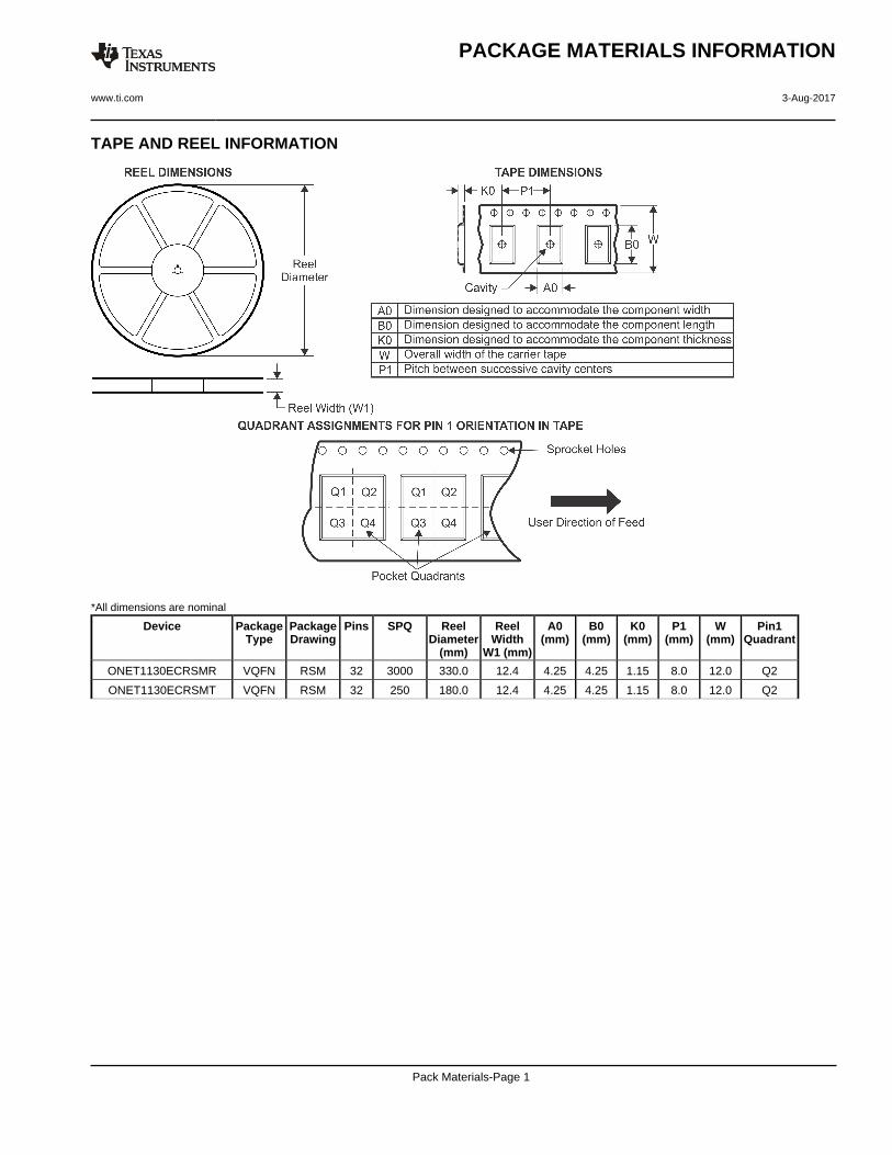
TAPE AND REEL INFORMATION
*All dimensions are nominal
Device PackageType
PackageDrawing
Pins SPQ ReelDiameter
(mm)
ReelWidth
W1 (mm)
A0(mm)
B0(mm)
K0(mm)
P1(mm)
W(mm)
Pin1Quadrant
ONET1130ECRSMR VQFN RSM 32 3000 330.0 12.4 4.25 4.25 1.15 8.0 12.0 Q2
ONET1130ECRSMT VQFN RSM 32 250 180.0 12.4 4.25 4.25 1.15 8.0 12.0 Q2
PACKAGE MATERIALS INFORMATION
www.ti.com 3-Aug-2017
Pack Materials-Page 1

*All dimensions are nominal
Device Package Type Package Drawing Pins SPQ Length (mm) Width (mm) Height (mm)
ONET1130ECRSMR VQFN RSM 32 3000 367.0 367.0 35.0
ONET1130ECRSMT VQFN RSM 32 250 210.0 185.0 35.0
PACKAGE MATERIALS INFORMATION
www.ti.com 3-Aug-2017
Pack Materials-Page 2


IMPORTANT NOTICE
Texas Instruments Incorporated (TI) reserves the right to make corrections, enhancements, improvements and other changes to itssemiconductor products and services per JESD46, latest issue, and to discontinue any product or service per JESD48, latest issue. Buyersshould obtain the latest relevant information before placing orders and should verify that such information is current and complete.TI’s published terms of sale for semiconductor products (http://www.ti.com/sc/docs/stdterms.htm) apply to the sale of packaged integratedcircuit products that TI has qualified and released to market. Additional terms may apply to the use or sale of other types of TI products andservices.Reproduction of significant portions of TI information in TI data sheets is permissible only if reproduction is without alteration and isaccompanied by all associated warranties, conditions, limitations, and notices. TI is not responsible or liable for such reproduceddocumentation. Information of third parties may be subject to additional restrictions. Resale of TI products or services with statementsdifferent from or beyond the parameters stated by TI for that product or service voids all express and any implied warranties for theassociated TI product or service and is an unfair and deceptive business practice. TI is not responsible or liable for any such statements.Buyers and others who are developing systems that incorporate TI products (collectively, “Designers”) understand and agree that Designersremain responsible for using their independent analysis, evaluation and judgment in designing their applications and that Designers havefull and exclusive responsibility to assure the safety of Designers' applications and compliance of their applications (and of all TI productsused in or for Designers’ applications) with all applicable regulations, laws and other applicable requirements. Designer represents that, withrespect to their applications, Designer has all the necessary expertise to create and implement safeguards that (1) anticipate dangerousconsequences of failures, (2) monitor failures and their consequences, and (3) lessen the likelihood of failures that might cause harm andtake appropriate actions. Designer agrees that prior to using or distributing any applications that include TI products, Designer willthoroughly test such applications and the functionality of such TI products as used in such applications.TI’s provision of technical, application or other design advice, quality characterization, reliability data or other services or information,including, but not limited to, reference designs and materials relating to evaluation modules, (collectively, “TI Resources”) are intended toassist designers who are developing applications that incorporate TI products; by downloading, accessing or using TI Resources in anyway, Designer (individually or, if Designer is acting on behalf of a company, Designer’s company) agrees to use any particular TI Resourcesolely for this purpose and subject to the terms of this Notice.TI’s provision of TI Resources does not expand or otherwise alter TI’s applicable published warranties or warranty disclaimers for TIproducts, and no additional obligations or liabilities arise from TI providing such TI Resources. TI reserves the right to make corrections,enhancements, improvements and other changes to its TI Resources. TI has not conducted any testing other than that specificallydescribed in the published documentation for a particular TI Resource.Designer is authorized to use, copy and modify any individual TI Resource only in connection with the development of applications thatinclude the TI product(s) identified in such TI Resource. NO OTHER LICENSE, EXPRESS OR IMPLIED, BY ESTOPPEL OR OTHERWISETO ANY OTHER TI INTELLECTUAL PROPERTY RIGHT, AND NO LICENSE TO ANY TECHNOLOGY OR INTELLECTUAL PROPERTYRIGHT OF TI OR ANY THIRD PARTY IS GRANTED HEREIN, including but not limited to any patent right, copyright, mask work right, orother intellectual property right relating to any combination, machine, or process in which TI products or services are used. Informationregarding or referencing third-party products or services does not constitute a license to use such products or services, or a warranty orendorsement thereof. Use of TI Resources may require a license from a third party under the patents or other intellectual property of thethird party, or a license from TI under the patents or other intellectual property of TI.TI RESOURCES ARE PROVIDED “AS IS” AND WITH ALL FAULTS. TI DISCLAIMS ALL OTHER WARRANTIES ORREPRESENTATIONS, EXPRESS OR IMPLIED, REGARDING RESOURCES OR USE THEREOF, INCLUDING BUT NOT LIMITED TOACCURACY OR COMPLETENESS, TITLE, ANY EPIDEMIC FAILURE WARRANTY AND ANY IMPLIED WARRANTIES OFMERCHANTABILITY, FITNESS FOR A PARTICULAR PURPOSE, AND NON-INFRINGEMENT OF ANY THIRD PARTY INTELLECTUALPROPERTY RIGHTS. TI SHALL NOT BE LIABLE FOR AND SHALL NOT DEFEND OR INDEMNIFY DESIGNER AGAINST ANY CLAIM,INCLUDING BUT NOT LIMITED TO ANY INFRINGEMENT CLAIM THAT RELATES TO OR IS BASED ON ANY COMBINATION OFPRODUCTS EVEN IF DESCRIBED IN TI RESOURCES OR OTHERWISE. IN NO EVENT SHALL TI BE LIABLE FOR ANY ACTUAL,DIRECT, SPECIAL, COLLATERAL, INDIRECT, PUNITIVE, INCIDENTAL, CONSEQUENTIAL OR EXEMPLARY DAMAGES INCONNECTION WITH OR ARISING OUT OF TI RESOURCES OR USE THEREOF, AND REGARDLESS OF WHETHER TI HAS BEENADVISED OF THE POSSIBILITY OF SUCH DAMAGES.Unless TI has explicitly designated an individual product as meeting the requirements of a particular industry standard (e.g., ISO/TS 16949and ISO 26262), TI is not responsible for any failure to meet such industry standard requirements.Where TI specifically promotes products as facilitating functional safety or as compliant with industry functional safety standards, suchproducts are intended to help enable customers to design and create their own applications that meet applicable functional safety standardsand requirements. Using products in an application does not by itself establish any safety features in the application. Designers mustensure compliance with safety-related requirements and standards applicable to their applications. Designer may not use any TI products inlife-critical medical equipment unless authorized officers of the parties have executed a special contract specifically governing such use.Life-critical medical equipment is medical equipment where failure of such equipment would cause serious bodily injury or death (e.g., lifesupport, pacemakers, defibrillators, heart pumps, neurostimulators, and implantables). Such equipment includes, without limitation, allmedical devices identified by the U.S. Food and Drug Administration as Class III devices and equivalent classifications outside the U.S.TI may expressly designate certain products as completing a particular qualification (e.g., Q100, Military Grade, or Enhanced Product).Designers agree that it has the necessary expertise to select the product with the appropriate qualification designation for their applicationsand that proper product selection is at Designers’ own risk. Designers are solely responsible for compliance with all legal and regulatoryrequirements in connection with such selection.Designer will fully indemnify TI and its representatives against any damages, costs, losses, and/or liabilities arising out of Designer’s non-compliance with the terms and provisions of this Notice.
Mailing Address: Texas Instruments, Post Office Box 655303, Dallas, Texas 75265Copyright © 2017, Texas Instruments Incorporated