of Electron Mobility in InSb QW-FETs
4
Atomi stic-Level Modeling for Thickness Dependence of Electron Mobility in InSb QW-FETs Ximeng Guan, Jing Lu, Yan Wang, and Zhiping Yu Institute of Microelectronics Tsinghua University Beijing 100084, China gxmgmails.tsinghua.edu.cn Abstract-The thickness dependence of electron mobility in the InSb quantum well (QW) FETs are calculated based on an atomistic approach for bandstructure calculation. The electron effective mass (m* ) is computed using fast yet accurate sp3d5s tight-binding (TB) method for InSb quantum-well (QW) (or ultra-thin-body, UTB) with thickness of 3-16 nm. The m dependence on the UTB thickness is then used in determining the electron mobility in the channel region of InSb QW-FETs. It is found that in QW-FETs, optical phonon scattering is a dominant factor, which is in turn strongly coupled to the carrier effective mass determined by channel thickness. The thickness dependence of electron mobility differs from that of the MOSFETs, where surface roughness is one of the major scattering mechanisms, Keywords - mobility; Indium Antimonide (InSb); ultra-thin- body (UTB); bandstructure; effectlive mass. I. INTRODUCTION InSb quantum-well (QW) transistors formed by AlInSb/InSb heterostructures are under spotlight recently due to its remarkable potential in low power/voltage and high- speed circuits [1]. It has been observed that to achieve the same performance as the state-of-the-art silicon MOSFETs, InSb QW-FETs consume about 10% in power owing to extremely high electron mobility (as high as 30,000 cm2 V-s) and saturation velocity (5 x107 cm/s ) in the channel region [2]. Although electron mobility for bulk InSb has already been studied, the modeling of effective electron mobility for InSb QW transistors calls for additional effort in two aspects. First, the quantum confinement in the thickness direction needs to be correctly and accurately calculated. Second, the difference in the scattering mechanisms of a InSb QW transistor from those of bulk materials should be studied. The difference in scattering mechanisms between InSb QW and Si MOSFETs have been studied in [3]. However, the strong quantum confinement in a nanoscaled InSb ultra-thin-body (UTB) and its impact on electron mobility needs further discussion. In this paper, the mobility of two-dimensional electron gas (2DEG) in InSb QW is calculated based on the bandstructure computation using the sp3ds* TB method [4]. The effective mass obtained is then used to determine the polar optical phonon scattering rate, which dominates the electron mobility. It is found that as the layer thickness decreases, so does the electron mobility in InSb channel region. II. DEVICE STRUCTURE The depletion mode InSb QW-FET studied in this paper is illustrated in Fig. 1. A a doped AlInSb barrier layer saves the carriers from Coulomb scattering caused by ionized impurities and provides carriers in channel at a zero gate voltage. The transistor thus works in a depletion mode with carriers confined in the InSb QW, as shown in Fig. 2. The device structure is also known as a modulation doped field-effective- transistor (MODFET). It has been demonstrated that when the mole fraction of Al increases to 30%0, the electron wavefunction is perfectly confined in the well [2]. Therefore, surface roughness scattering does not play a major role in determining the carrier mobility in the channel [3], in contrast to surface mode devices like Si MOSFETs. Figure 1. The AlInSb/InSb Quantum Well Transistor studied in this work. The mole fraction of Al in the barrier layer is set to 30% (i.e., x = y = 0.3). III. APPROACHES Different approaches have been developed for carrier mobility simulation. One of the most commonly adopted schemes is based on the Monte Carlo method, which randomly select from different scattering mechanisms at the end of each free flight. The mobility calculated then converges to a constant value after enough time of simulation. Although the This work is supported by a grant from National Science Foundation in China (Computational Nanoelectronics, # 90307016). The grant from Foundation for Ph.D. studies of Chinese Ministry of Education is also greatly appreciated. 1-4244-0404-5/06/$20.00 © 2006 IEEE SISPAD 2006 248
Transcript of of Electron Mobility in InSb QW-FETs
Atomistic-Level Modeling for Thickness Dependence
of Electron Mobility in InSb QW-FETsXimeng Guan, Jing Lu, Yan Wang, and Zhiping Yu
Institute of MicroelectronicsTsinghua University
Beijing 100084, Chinagxmgmails.tsinghua.edu.cn
Abstract-The thickness dependence of electron mobility in theInSb quantum well (QW) FETs are calculated based on anatomistic approach for bandstructure calculation. The electroneffective mass (m* ) is computed using fast yet accurate sp3d5stight-binding (TB) method for InSb quantum-well (QW) (orultra-thin-body, UTB) with thickness of 3-16 nm. Them dependence on the UTB thickness is then used in determiningthe electron mobility in the channel region of InSb QW-FETs. Itis found that in QW-FETs, optical phonon scattering is adominant factor, which is in turn strongly coupled to the carriereffective mass determined by channel thickness. The thicknessdependence of electron mobility differs from that of theMOSFETs, where surface roughness is one of the majorscattering mechanisms,
Keywords - mobility; Indium Antimonide (InSb); ultra-thin-body (UTB); bandstructure; effectlive mass.
I. INTRODUCTIONInSb quantum-well (QW) transistors formed by
AlInSb/InSb heterostructures are under spotlight recently dueto its remarkable potential in low power/voltage and high-speed circuits [1]. It has been observed that to achieve the sameperformance as the state-of-the-art silicon MOSFETs, InSbQW-FETs consume about 10% in power owing to extremelyhigh electron mobility (as high as 30,000 cm2 V-s) andsaturation velocity (5 x107 cm/s ) in the channel region [2].Although electron mobility for bulk InSb has already beenstudied, the modeling of effective electron mobility for InSbQW transistors calls for additional effort in two aspects. First,the quantum confinement in the thickness direction needs to becorrectly and accurately calculated. Second, the difference inthe scattering mechanisms of a InSb QW transistor from thoseof bulk materials should be studied. The difference inscattering mechanisms between InSb QW and Si MOSFETshave been studied in [3]. However, the strong quantumconfinement in a nanoscaled InSb ultra-thin-body (UTB) andits impact on electron mobility needs further discussion.
In this paper, the mobility of two-dimensional electron gas(2DEG) in InSb QW is calculated based on the bandstructurecomputation using the sp3ds* TB method [4]. The effectivemass obtained is then used to determine the polar opticalphonon scattering rate, which dominates the electron mobility.
It is found that as the layer thickness decreases, so does theelectron mobility in InSb channel region.
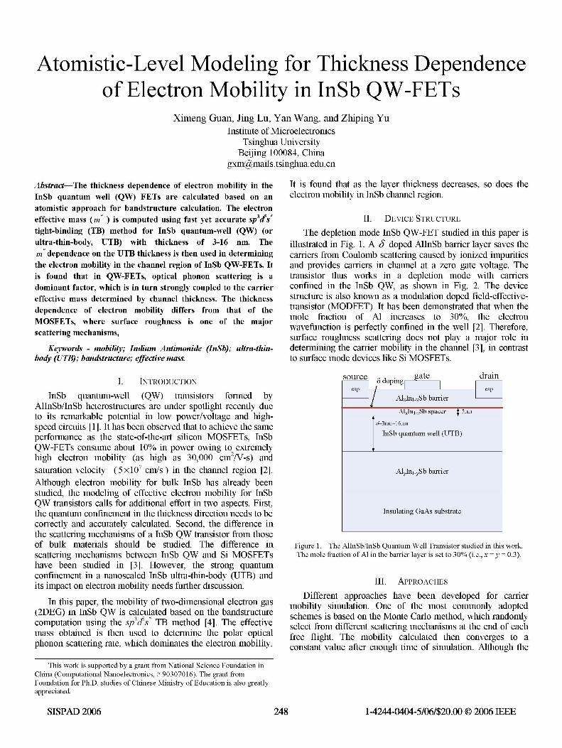
II. DEVICE STRUCTUREThe depletion mode InSb QW-FET studied in this paper is
illustrated in Fig. 1. A a doped AlInSb barrier layer saves thecarriers from Coulomb scattering caused by ionized impuritiesand provides carriers in channel at a zero gate voltage. Thetransistor thus works in a depletion mode with carriersconfined in the InSb QW, as shown in Fig. 2. The devicestructure is also known as a modulation doped field-effective-transistor (MODFET). It has been demonstrated that when themole fraction of Al increases to 30%0, the electronwavefunction is perfectly confined in the well [2]. Therefore,surface roughness scattering does not play a major role indetermining the carrier mobility in the channel [3], in contrastto surface mode devices like Si MOSFETs.
Figure 1. The AlInSb/InSb Quantum Well Transistor studied in this work.The mole fraction ofAl in the barrier layer is set to 30% (i.e., x = y = 0.3).
III. APPROACHESDifferent approaches have been developed for carrier
mobility simulation. One of the most commonly adoptedschemes is based on the Monte Carlo method, which randomlyselect from different scattering mechanisms at the end of eachfree flight. The mobility calculated then converges to aconstant value after enough time of simulation. Although the
This work is supported by a grant from National Science Foundation inChina (Computational Nanoelectronics, # 90307016). The grant fromFoundation for Ph.D. studies of Chinese Ministry of Education is also greatlyappreciated.
1-4244-0404-5/06/$20.00 © 2006 IEEESISPAD 2006 248
method has been approved for accurate mobility calculation, itdoes not relate the average electron mobility and scatteringprobability for each mechanism in an analytical way, and thusdoes not give a direct insight into the impacts of differentscattering mechanisms and potential changes caused bybandstructure distortion.
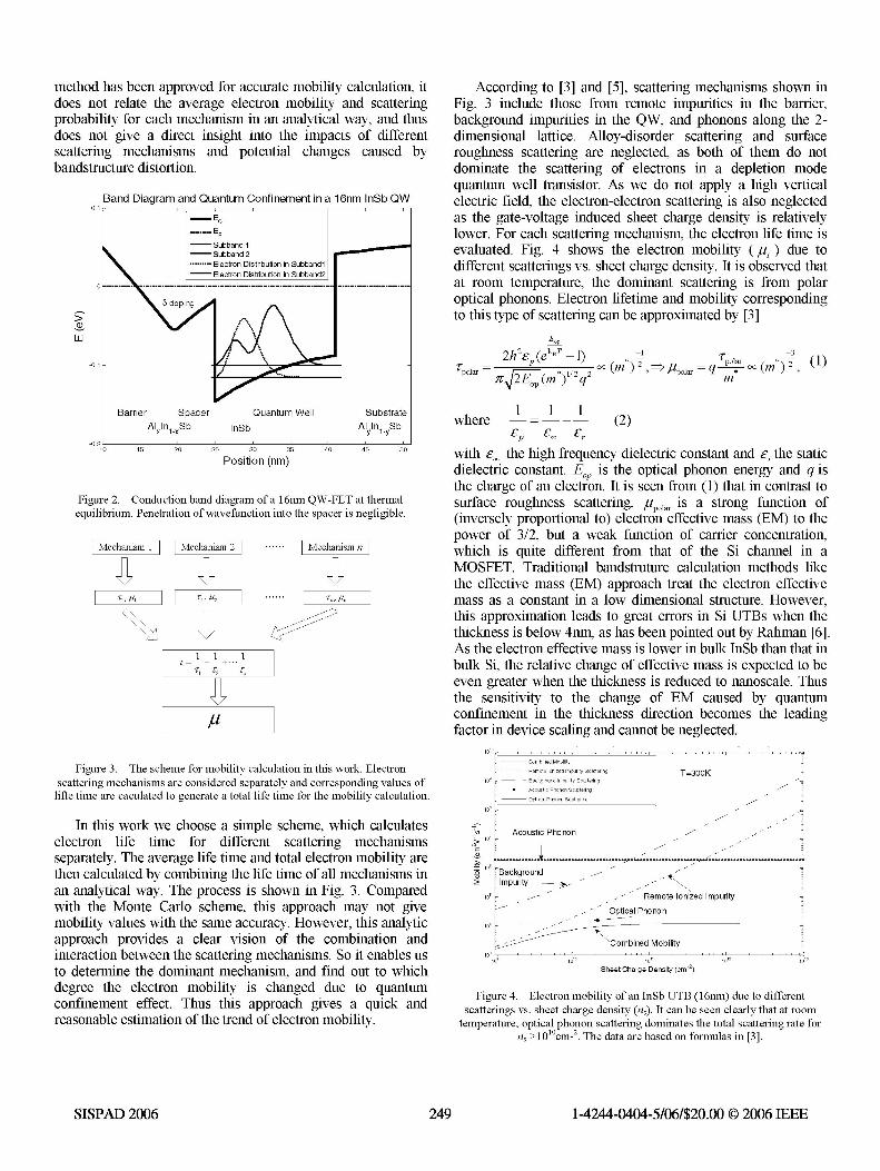
Band Diagram and Quantum Confinement in a 16nm InSb QW
ci)uJ]
According to [3] and [5], scattering mechanisms shown inFig. 3 include those from remote impurities in the barrier,background impurities in the QW, and phonons along the 2-dimensional lattice. Alloy-disorder scattering and surfaceroughness scattering are neglected, as both of them do notdominate the scattering of electrons in a depletion modequantum well transistor. As we do not apply a high verticalelectric field, the electron-electron scattering is also neglectedas the gate-voltage induced sheet charge density is relativelylower. For each scattering mechanism, the electron life time isevaluated. Fig. 4 shows the electron mobility (y,1 ) due todifferent scatterings vs. sheet charge density. It is observed thatat room temperature, the dominant scattering is from polaroptical phonons. Electron lifetime and mobility correspondingto this type of scattering can be approximated by [3]
2h2 (ekBT 1)Tpolar 2E(m*)1/2 q2 (m) 2 , > 'polar -q plar (* (1)
m
-0.2L10
Barrier Spacer Quantum Well
Alx n1 xSb nSb
15 20 25 30 35
Position (nm)
Figure 2. Conduction band diagram of a 16nm QNequilibrium. Penetration ofwavefunction into the sp
Mechansm VMechanism 2
TA,TA fl2
...... Fme
...
1 11'C =-+-+ .. ._
1C C2 C,
SubstrateAl InSbyI -y
1 _1 1where I -
I Er£p £c£r--
(2)
40 45 50 with Ec the high frequency dielectric constant and Er the staticdielectric constant. Eo is the optical phonon energy and q isthe charge of an electron. It is seen from (1) that in contrast to
Af-FET at thermal surface roughness scattering,/'pola is a strong function ofzacer iS negligible. (inversely proportional to) electron effective mass (EM) to the
power of 3/2, but a weak function of carrier concentration,chanism n which is quite different from that of the Si channel in a
MOSFET. Traditional bandstruture calculation methods likethe effective mass (EM) approach treat the electron effective
rn, Un/ mass as a constant in a low dimensional structure. However,this approximation leads to great errors in Si UTBs when thethickness is below 4nm, as has been pointed out by Rahman [6].As the electron effective mass is lower in bulk InSb than that inbulk Si, the relative change of effective mass is expected to beeven greater when the thickness is reduced to nanoscale. Thusthe sensitivity to the change of EM caused by quantumconfinement in the thickness direction becomes the leadingfactor in device scaling and cannot be neglected.
Figure 3. The scheme for mobility calculation in this work. Electronscattering mechanisms are considered separately and corresponding values oflifte time are caculated to generate a total life time for the mobility calculation.
_:| Combine.d Mobility|. - - - Remo.te lonized Impunty Scadtterng
109 - Background Impunty Scttenng* Acoustic Phonon Scattenng
Optical Ph.,,., Scattering
T=300K
In this work we choose a simple scheme, which calculateselectron life time for different scattering mechanismsseparately. The average life time and total electron mobility arethen calculated by combining the life time of all mechanisms inan analytical way. The process is shown in Fig. 3. Comparedwith the Monte Carlo scheme, this approach may not givemobility values with the same accuracy. However, this analyticapproach provides a clear vision of the combination andinteraction between the scattering mechanisms. So it enables usto determine the dominant mechanism, and find out to whichdegree the electron mobility is changed due to quantumconfinement effect. Thus this approach gives a quick andreasonable estimation of the trend of electron mobility.
Q)
10
*51o
Acoustic Phonon -I I
| / ,~~~~~~I..1..... .............. .......... ...............
BackgroundImpurity -*
Remote Ionized ImpurityOptical Phonon
Combined Mobility103
109 1010 1 10'2 1013Sheet Charge Density (cm-2
Figure 4. Electron mobility of an InSb UTB (16nm) due to differentscatterings vs. sheet charge density (n,). It can be seen clearly that at room
temperature, optical phonon scattering dominates the total scattering rate forn, >l'0 cm-2. The data are based on formulas in [3].
1-4244-0404-5/06/$20.00 0 2006 IEEESISPAD 2006 249
In this work, we employ an atomistic approach inbandstructure calculation, based on the sp3cds* tight-bindingmodel. The approach has been successfully applied in Si/Genanowires [7], and Fig. 5 shows its application in an InSb UTBwith 6 atom layers. Table 1 shows the Hamiltonian matrix ofthis UTB, resulting from our approach.
[100]
3* * * 0 0 * * Amion or
4 0 0 0 0 0 00
typeIatom
Cation or
5* * * 0 0 0 * 0 type 2 atom
6 O ) ) ( ( (
employed in estimating sheet charge densities for different gatevoltages.
IV. RESULTS AND DISCUSSIONS
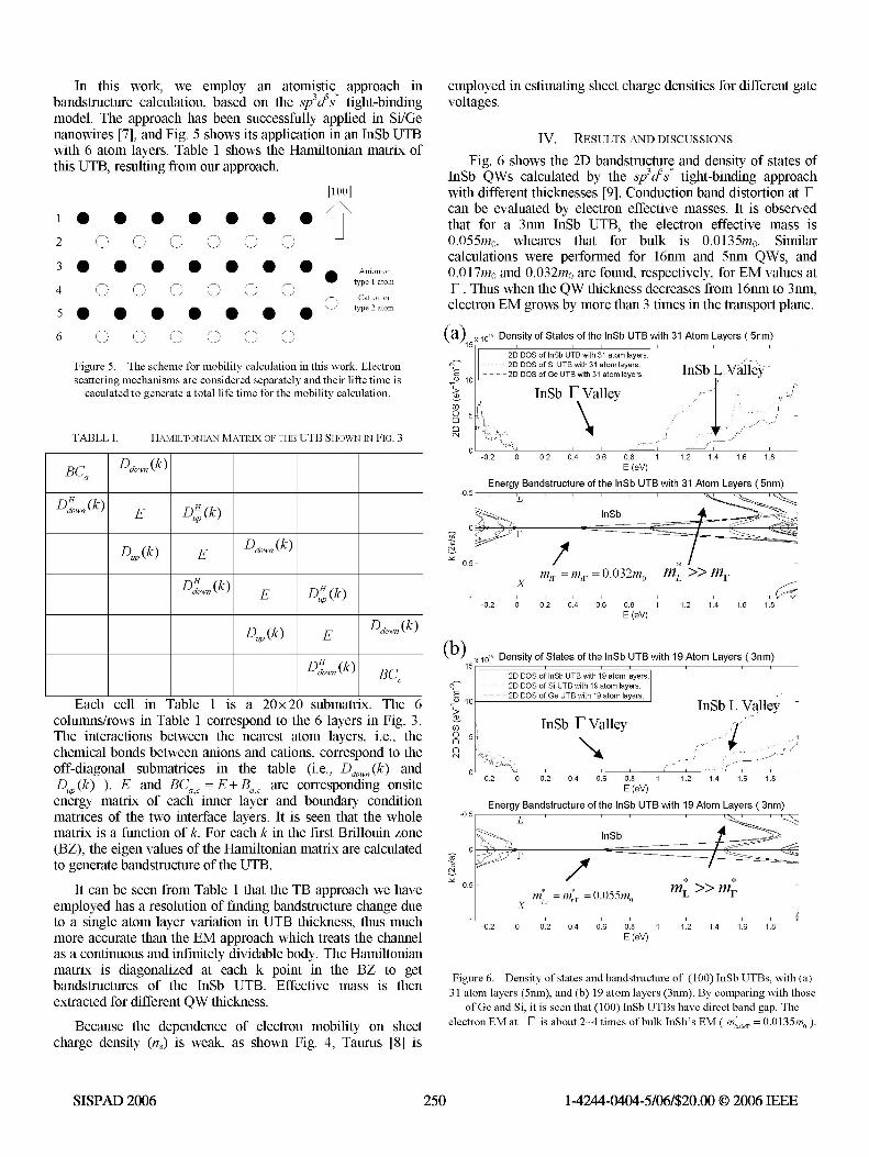
Fig. 6 shows the 2D bandstructure and density of states ofInSb QWs calculated by the sp3cds* tight-binding approachwith different thicknesses [9]. Conduction band distortion at Fcan be evaluated by electron effective masses. It is observedthat for a 3nm InSb UTB, the electron effective mass is0.055mo, wheares that for bulk is 0.0135mo. Similarcalculations were performed for 16nm and 5nm QWs, and0.017mo and 0.032mo are found, respectively, for EM values atF. Thus when the QW thickness decreases from 16nm to 3nm,electron EM grows by more than 3 times in the transport plane.
(a) X 1ol5 Density of States of the InSb UTB with 31 Atom Layers ( 5nm)151
Figure 5. The scheme for mobility calculation in this work. Electronscattering mechanisms are considered separately and their lifte time is
caculated to generate a total life time for the mobility calculation.
TABLE I. HAMILTONIAN MATRIX OF THE UTB SHOWN iN FIG. 3
BC | Ddowf(k)
DUp(k) E Ddowf(k)
DH, (k) E DH(k)
DEp(k) E Ddowfk(k)t ,,,, Ddk) , (k)
DdL,(k) BC,Each cell in Table 1 is a 20x20 submatrix. The 6
columns/rows in Table 1 correspond to the 6 layers in Fig. 3.The interactions between the nearest atom layers, i.e., thechemical bonds between anions and cations, correspond to theoff-diagonal submatrices in the table (i.e., Ddowfl (k) andDup (k) ). E and BCac = E + Ba,c are corresponding onsiteenergy matrix of each inner layer and boundary conditionmatrices of the two interface layers. It is seen that the wholematrix is a function of k. For each k in the first Brillouin zone(BZ), the eigen values of the Hamiltonian matrix are calculatedto generate bandstructure of the UTB.
It can be seen from Table 1 that the TB approach we haveemployed has a resolution of finding bandstructure change dueto a single atom layer variation in UTB thickness, thus muchmore accurate than the EM approach which treats the channelas a continuous and infinitely dividable body. The Hamiltonianmatrix is diagonalized at each k point in the BZ to getbandstructures of the InSb UTB. Effective mass is thenextracted for different QW thickness.
Because the dependence of electron mobility on sheetcharge density (ns) is weak, as shown Fig. 4, Taurus [8] is
.E-ID 10
D5)0 5
20D DOS of InSb UTB with 31 atom layers.2D DOS of Si UTB with 31 atom layers.2D DOS of Ge UTB with 31 atom layers.
InSb F Valley
-02 0 02 04 06 08E (eV)
InSb L.Valley-
1.2 1.4 1.6 1.8
Energy Bandstructure of the InSb UTB with 31 Atom Layers (5nm)-0.5 I ~L IIIX
InSb
o0.
mx = mtr = 0.032mo mL >> m,
-02 0 02 04 06 08 1 1.2 1.4 1.6E (eV)
1.8
(b) X 1015 Density of States of the InSb UTB with 19 Atom Layers ( 3nm)15,
(N
Eo 10 -
U)o 5 t
CN
2D DOS of InSb UTB with 19 atom layers.2D DOS of Si UTB with 19 atom layers.2D DOS of Ge UTB with 19 atom layers.
InSb F ValleyInSb L Valley
-0.2 0 0.2 0.4 0.6 0.8 1 1.2 1.4 1.6 1.8E (eV)
Energy Bandstructure of the InSb UTB with 19 Atom Layers (3nm)
InSb
ml =mtr 0.055mo L r
-02 0 02 04 06 08 1 1.2 1.4 1.6 1.8E (eV)
Figure 6. Density of states and bandstructure of (100) InSb UTBs, with (a)31 atom layers (5nm), and (b) 19 atom layers (3nm). By comparing with those
ofGe and Si, it is seen that (100) InSb UTBs have direct band gap. Theelectron EM at F is about 2-4 times of bulk InSb's EM ( m' = 0.0135mo ).
1-4244-0404-5/06/$20.00 © 2006 IEEE
r-
-Y
SISPAD 2006 250
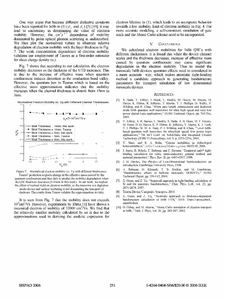
One may argue that because different dielectric constantshave been reported for InSb in (1) ( and e,.) [3] [10], it maylead to uncertainty in determining the value of electronmobility. However, the (m*)-3 2 dependence of mobilitydominated by polar optical phonon scattering is undistrurbed.We thus plot the normalized values to illustrate relativedegradation of electron mobility with the layer thickness in Fig.7. The weak concentration dependence of electron mobilityvalidates our employment of Taurus as a first-order estimatorfor sheet charge density (ns).
Fig. 7 shows that according to our calculation, the electronmobility decreases as the thickness of the UTB increases. Thisis due to the increase of effective mass when quantumconfinement induces distortion in the conduction band valley.However, the quantum box in Taurus which is based on theeffective mass approximation indicates that the mobilityincreases when the channel thickness is shrunk from 15nm to3nm.
Normalized Electron Mobility vs. Vg with Different Channel Thicknesses0.4
0.35 _. _9~
0.3
0.25 e Well Thickness0 Well Thickness
0.2 Well ThicknessWell Thickness
0.15 El Well Thickness:
RO=7x1 04cm/Ns
1 6nm, this work1 6nm, Taurus5nm, this work5nm, Taurus3nm, this work
-0 .4 -0 .3 -0.2 -0.( 1
Vg9 (V)
Figure 7. Normalized electron mobility vs. Vg with different thicknesses.Taurus' prediction neglects change in the effective mass caused by the
quantum confinement and thus fails to predict the mobility degradation whenthe QW thickness decreases (3-16nm in this work). In our work, we neglectthe effect of vertical field on electron mobility, as the transistor is a depletion
mode device and surface scattering is not dominating the transport ofelectrons. The results from Taurus validate the approximation we take.
It is seen from Fig. 7 that the mobility does not exceeds104cm2/Vs. However, experiments by Datta [1] have shown ameasured electron of mobility of 32000 cm2 Vs. We find thatthe relatively smaller mobility calculated by us is due to theapproximations used in deriving the analytic expression for
electron lifetime in (1), which leads to an asymptotic behaviortowards a low mobility limit of electron mobility in Fig. 4. Formore accurate modeling, a self-consistent simulation of gatestack and the Monte Carlo scheme need to be incorporated.
V. CONCLUSIONS
We calculated electron mobilities for InSb QW's withdifferent thicknesses. It is found that while the device channelscales and the thickness decreases, increase of effective masscaused by quantum confinement may cause significantdegradation in the electron mobility. Thus to model thenanoscale InSb devices, quantum effects need to considered ina more accurate way, which makes atomistic tight-bindingmethod a candidate approach to generating bandstructureparameters for transport simulation of low dimensionalnanoscale devices.
REFERENCES[1] S. Datta, T. Ashley, J. Brask, L. Buckle, M. Doczy, M. Emeny, D.
Hayes, K. Hilton, R. Jefferies, T. Martin, T. J. Phillips, D. Wallis, P.Wilding, and R. Chau, "85nm gate length enhancement and depletionmode InSb quantum well transistors for ultra high speed and very lowpower digital logic applications," IEDM Technical Digest, pp. 763-766,2005.
[2] T. Ashley, A. R. Barnes, L. Buckle, S. Datta, A. B. Dean, M. T. Emeny,M. Fearn, D. G. Hayes, K. P. Hilton, R. Jefferies, T. Martin, K. J. Nash,T. J. Phillips, W. H. A. Tang, P. J. Wilding, and R. Chau, "Novel InSb-based quantum well transistors for ultra-high speed, low power logicapplications," 7th Int'l Conf. on Solid-State and Integrated CircuitsTechnology (ICSICT) Proceedings, vol. 3, p. 2253-2256, 2004.
[3] Y. Shao, and S. A. Solin, "Carrier mobilities in delta-dopedheterostructures," ArXiv Condensed Matter e-prints, 0602140, 2006.
[4] J. Jancu, R. Scholz, F. Beltram, and F. Bassani, "Empirical spds* tight-binding calculation for cubic semiconductors: general method andmaterial parameters," Phys. Rev. B, pp. 6493-6507, 1998.
[5] J. H. Davies, The Physics of Low-Dimensional Semiconductors: anIntroduction, Cambridge University Press, 1998.
[6] A. Rahman, G. Klimeck, T. B. Boykin, and M. Lundstrom,"Bandstructure effects in ballistic nanoscale MOSFETs," IEDMTechnical Digest, pp. 139-142, 2004.
[7] X. Guan, and Z. Yu, "Supercell approach in tight-binding calculation ofSi and Ge nanowire bandstructures," Chin. Phys. Lett., vol. 22, pp.265 1-2654, 2005.
[8] Taurus Device Userguide, Synopsys, 2003.[9] X. Guan, and Z. Yu, "Atomistic approach to thickness-dependent
bandstructure calculation of InSb UTB," IEEE Trans.Nanotechnol.,unpublished.
[10] 0. Ozba*, and M. Akarsu, "Monte Carlo simulation of electron transportin InSb," Turk. J. Phys., vol. 26, pp. 283-287, 2002.
1-4244-0404-5/06/$20.00 © 2006 IEEE
0.1
0.05-
0.1
SISPAD 2006 251


![Strained -Sn on InSb(001) · InSb, is likewise a heteroepitaxial strained system. The use of InSb as a template for high quality crystals is well established [18{20]. It induces a](https://static.fdocuments.net/doc/165x107/5f63835e50764f10ad37eb67/strained-sn-on-insb001-insb-is-likewise-a-heteroepitaxial-strained-system-the.jpg)