Mechanisms of Silicide Formation by Reactive Diffusion in ...

Observation on Isothermal Reactive Diffusion between Solid Ni and Liquid Sn
Akihiro Nakane1, Takao Suzuki1, Minho O2 and Masanori Kajihara2,*
1Graduate School, Tokyo Institute of Technology, Yokohama 226–8502, Japan2Department of Materials Science and Engineering, Tokyo Institute of Technology
The kinetics of the reactive diffusion between solid Ni and liquid Sn was experimentally examined using Ni/Sn diffusion couples. The diffusion couples were prepared by an isothermal bonding technique and then immediately annealed in the temperature range of T = 533–623 K for various times up to t = 14.4 ks (4 h). During annealing, a compound layer of Ni3Sn4 is formed at the original Ni/Sn interface in the diffusion couple and grows mainly into the liquid Sn specimen. The mean thickness of the compound layer is proportional to a power function of the annealing time. The exponent n of the power function takes values between 0.31 and 0.43. Since there is no systematic dependence of n on T, we may consider that n is insensitive to T within experimental uncertainty. When growth of a compound layer with uniform thickness is con-trolled by volume diffusion, n is equivalent to 0.5. If boundary diffusion contributes to the layer growth and grain growth occurs in the compound layer, however, n becomes smaller than 0.5. Since grain growth practically takes place in the compound layer, it is concluded that the layer growth of Ni3Sn4 is mainly controlled by boundary diffusion at T = 533–623 K. [doi:10.2320/matertrans.MD201510]
(Received December 8, 2015; Accepted February 1, 2016; Published March 18, 2016)
Keywords: reactive diffusion, intermetallic compounds, soldering, bulk diffusion, Ni–Sn system
1. Introduction
Owing to high electrical conductivity, Cu-base alloys are widely used as conductor materials in the electronics indus-try. When the Cu-base conductor is interconnected with a Sn-base solder, Cu6Sn5 and Cu3Sn are formed at the interconnec-tion between the conductor and the solder during soldering and then gradually grow during energization heating at sol-id-state temperatures.1–11) Since the Cu–Sn compounds are brittle and possess high electrical resistivities, their growth deteriorates the mechanical and electrical properties of the interconnection. To inhibit the formation of the compounds, the Cu-base conductor is usually plated with a Ni layer. How-ever, Ni is not suf�ciently corrosion resistant. Hence, the Ni layer is plated with a Au or Pd layer to improve corrosion re-sistance.12–15)
For the multilayer Au/Ni/Cu conductor with a thin Au lay-er, the Au layer quickly dissolves into a molten Sn-base sol-der during soldering, and then the Ni layer is contacted with the solder. As a consequence, the Ni layer is directly reacted with the solder during soldering and solid-state energization heating. As to a phenomenon during energization heating, the solid-state reactive diffusion in the Ni/Sn system was experi-mentally examined using sandwich Sn/Ni/Sn diffusion cou-ples prepared by a diffusion bonding technique in a previous study.16) In this experiment, the diffusion couples were iso-thermally annealed at temperatures of T = 433–473 K. At the interface in the annealed diffusion couple, a layer of Ni3Sn4 was observed at T = 453–473 K, but granular particles of Ni3Sn4 were recognized at T = 433 K. The mean thickness of the Ni3Sn4 layer is proportional to a power function of the annealing time. The exponent of the power function is 0.46 and 0.41 at T = 453 and 473 K, respectively. The exponent smaller than 0.5 indicates that the growth of Ni3Sn4 is con-trolled by boundary and volume diffusion and grain growth occurs in Ni3Sn4. Although the growth of Ni3Sn4 may be ac-celerated by boundary diffusion, the overall growth rate is
smaller for Ni3Sn416) than for Cu6Sn5 and Cu3Sn.3,11) Conse-
quently, the Ni layer works as a barrier against the reactive diffusion at the interconnection between the Sn-base solder and the multilayer Au/Ni/Cu conductor with a thin Au layer during solid-state energization heating.
On the other hand, during soldering, the Ni layer is reacted with the molten Sn-base solder at the interconnection. The reactive diffusion between solid Ni and liquid Sn was experi-mentally observed by Kang and Ramachandran17) using Ni/Sn diffusion couples prepared by an immersion technique in the temperature range of T = 573–773 K. During annealing, an intermetallic layer composed of Ni3Sn4 and Ni3Sn2 is formed at the original interface in the Ni/Sn diffusion couple, where the thickness of the Ni3Sn2 layer is much smaller than that of the Ni3Sn4 layer. In contrast, a soldering technique was used by Lin et al.18) to observe experimentally the reactive diffusion between solid Ni and liquid Sn at temperatures of T = 523–553 K. In their experiment, however, an intermetal-lic layer consisting of only Ni3Sn4 is produced at the original interface in the Ni/Sn diffusion couple. The temperature range is lower for the experiment by Lin et al.18) than for that by Kang and Ramachandran.17) Furthermore, an immersion technique was used by Kang and Ramachandran,17) but a sol-dering technique was utilized by Lin et al.18) Thus, the forma-tion of Ni3Sn2 may be sensitive to the annealing temperature and/or the preparation technique of diffusion couple.
Kinetics of reactive diffusion between various solid and liquid metals was experimentally observed using an isother-mal bonding (IB) technique in previous studies.19–22) In the IB technique, the solid and liquid metals are separately pre-heated at the same temperature as the isothermal annealing temperature in a vacuum. After suf�cient preheating, the sol-id and liquid metals are bonded with each other and then an-nealed immediately. Thus, unlike immersion and soldering techniques, the temperatures of the solid and liquid metals are equivalent and remain constant during preheating, bonding and annealing in the IB technique. In the present study, the IB technique was used to observe experimentally kinetics of the reactive diffusion between solid Ni and liquid Sn. Diffusion * Corresponding author, E-mail: [email protected]
Materials Transactions, Vol. 57, No. 6 (2016) pp. 838 to 845 Special Issue on Frontier Researches Related to Interconnection, Packaging and Microjoining Materials and Microprocessing for Such Materials ©2016 The Japan Institute of Metals and Materials

couples consisting of pure Ni and Sn specimens were pre-pared by the IB technique and then isothermally annealed in the temperature range of T = 533–623 K. The microstructure of the annealed diffusion couple was observed in a metallo-graphical manner. The rate-controlling process of the com-pound growth was discussed on the basis of the observation.
2. Experimental
Polycrystalline columnar specimens with length of 5 mm were cut from a commercial rod of pure Ni with diameter of 8 mm and purity higher than 99% in a manner similar to a previous study.22) The columnar specimens were separately annealed in evacuated silica capsules at a temperature of 1173 K for a time of 2 h, followed by air cooling without breaking the capsules. The top and bottom �at-surfaces of each annealed columnar specimen were mechanically pol-ished on # 800–4000 emery papers.
A commercial rod of pure Sn with diameter of 6 mm and purity of 99.9% was cut into columnar specimens with length of 30 mm. Each polished Ni specimen was encapsulated to-gether with a columnar Sn specimen in an evacuated silica capsule with inner diameter of 8.5 mm. The silica capsule was isothermally preheated for a time of 1.8 ks (0.5 h) in the temperature range between 533 K and 623 K. During pre-heating, the solid Ni specimen was separated from the Sn melt in the silica capsule. After preheating, a �at surface of the solid Ni specimen was immediately contacted with that of the Sn melt with diameter of 8.5 mm and length of 15 mm to prepare a columnar Ni/Sn diffusion couple. The diffusion couple was isothermally annealed for various times up to 14.4 ks (4 h) at the same temperature as preheating, followed by water quenching with breaking the capsule. The annealing temperature and time are denoted by T and t, respectively.
Cross-sections of the annealed diffusion couple were me-chanically polished on # 800–4000 emery papers and then �nished using diamond with diameter of 1 μm. The micro-structure of the cross-section was observed by differential interference contrast optical microscopy (DICOM) and with a back-scattered electron image (BEI) by scanning electron microscopy (SEM). Concentrations of Ni and Sn in each phase on the cross-section were measured by electron probe microanalysis (EPMA) using pure Ni and Sn with purity of 99.99% as standard specimens under the following condi-tions: the accelerating voltage was 20 kV; the probe current was 5 nA; the analyzing crystals for Ni-Kα and Sn-Lα were lithium �uoride (LiF) and polyethylene terephthalate (PET), respectively; and the chemical composition was evaluated by a standard ZAF correction technique.
3. Results and Discussion
3.1 MicrostructureA cross-sectional DICOM image of a diffusion couple an-
nealed at T = 533 K for t = 1.2 ks (20 min) is shown in Fig. 1. In this �gure, the lower and upper regions are the Ni and Sn specimens, respectively. As can be seen, a compound layer with a slightly different contrast is observed between the Ni and the Sn. Concentration pro�les of Ni and Sn across the compound layer along the direction normal to the original
Ni/Sn interface were measured by EPMA. A result for a dif-fusion couple with T = 583 K and t = 3.6 ks (1 h) is indicated in Fig. 2. In this �gure, the ordinate and the abscissa show the mol fraction yi of component i and the distance x, respective-ly, and open squares and circles indicate the mol fractions yNi and ySn, respectively. In Fig. 2, the origin x = 0 of the distance is located in the Ni. For the EPMA measurement, however, attention was focused on phase identi�cation of the com-pound layer. Consequently, the location of the origin is mere-ly arbitrarily chosen to represent conveniently the concentra-tion pro�les. As can be seen, the compound layer is Ni3Sn4. According to a recent phase diagram in the binary Ni–Sn sys-tem,23) Ni3Sn, Ni3Sn2 and Ni3Sn4 are the stable compounds at T = 533–623 K. Nevertheless, only Ni3Sn4 was observed in all the annealed diffusion couples. The Ni3Sn4 layer grows
Fig. 1 DICOM image of cross-section for the diffusion couple annealed at T = 533 K for t = 1.2 ks (20 min).
Fig. 2 Concentration pro�les of Ni and Sn across the intermetallic layer along the direction normal to the original Ni/Sn interface for the diffusion couple annealed at T = 583 K for t = 3.6 ks (1 h).
839Observation on Isothermal Reactive Diffusion between Solid Ni and Liquid Sn

mainly towards the Sn in the diffusion couple.The spatial resolution of EPMA is about 1 μm. If the thick-
ness of a compound is much smaller than the spatial resolu-tion, the compound cannot be detected by EPMA. When the interdiffusion coef�cient of a compound is very small, the compound cannot grow to detectable thicknesses within real-istic annealing times.24–33) A diffusion couple technique has been conveniently used by many researchers to determine phase diagrams in multicomponent systems. In this tech-nique, however, all the stable compounds may not be neces-sarily observed under experimental conditions.34–42) There-fore, stable compounds with very small interdiffusion coef�cients are missing in the phase diagram. Consequently, it is rather dangerous to determine the phase diagram only by the diffusion couple technique. The microstructure observa-tion of the annealed Ni/Sn diffusion couple implies that the interdiffusion coef�cient is much smaller for Ni3Sn and Ni3Sn2 than for Ni3Sn4.
3.2 Growth behavior of intermetallic layerIn cross-sectional DICOM images such as that shown in
Fig. 1, the Ni3Sn4 layer is distinguishable from the Ni and the Sn. Hereafter, the Ni3Sn4 layer is called the intermetallic lay-er. A schematic microstructure of the intermetallic layer on cross-section i is shown in Fig. 3. From the DICOM image, the area Ai of the intermetallic layer corresponding to the par-tial length wi of the original Ni/Sn interface in Fig. 3 was measured on each cross-section, and then the sums A and w were obtained as22)
A =m
i=1
Ai (1a)
and
w =m
i=1
wi (1b)
from Ai and wi, respectively, where m ≥ 5. Using the values of A and w, the mean thickness l of the intermetallic layer was evaluated at each annealing time t by the following equa-tion:22)
l =Aw. (2)
The results for T = 533, 583, 603, 613 and 623 K are indicated as open triangles, rhombuses, squares, inverse-triangles and circles, respectively, in Fig. 4. In this �gure, the ordinate and the abscissa show the logarithms of l and t, respectively. As can be seen, most of the experimental points are located well on a straight line at each annealing temperature. This means that l is expressed as a power function of t by the following equation.
l = ktt0
n
(3)
Here, t0 is unit time, 1 s. It is adopted to make the argument t/t0 of the power function dimensionless. The proportionality coef�cient k has the same dimension as the thickness l, but the exponent n is dimensionless. The dimensionless argument of the power function is essentially important; otherwise the dimension of k varies depending on the value of n. From the experimental points in Fig. 4, k and n were estimated by the least-squares method as shown with various straight lines. The estimated values are indicated in Fig. 4.
As mentioned in Section 1, the reactive diffusion between solid Ni and liquid Sn was experimentally observed by Kang and Ramachandran17) using an immersion technique in the
Fig. 3 Schematic microstructure of intermetallic layer on cross-section i.Fig. 4 The thickness l of the intermetallic layer versus the annealing time t.
Open triangles, rhombuses, squares, inverse-triangles and circles show the results for T = 533, 583, 603, 613 and 623 K, respectively. Various lines represent the calculations from eq. (3).
840 A. Nakane, T. Suzuki, M. O and M. Kajihara

temperature range of T = 573–773 K. In their experiment, a pure Ni sheet with dimensions of 50 mm × 10 mm × 1 mm was immersed into molten pure Sn with weight of 50 g and then annealed for various periods up to 28.8 ks (8 h). During annealing, an intermetallic layer composed of Ni3Sn4 and Ni3Sn2 is formed at the original interface in the Ni/Sn diffu-sion couple, where the thickness of the Ni3Sn2 layer is much smaller than that of the Ni3Sn4 layer. As mentioned in Section 3.1, the interdiffusion coef�cient is much smaller for Ni3Sn and Ni3Sn2 than for Ni3Sn4. In the experiment by Kang and Ramachandran,17) however, Ni3Sn2 was observed but Ni3Sn was not recognized. This means that the interdiffusion coef�-cient of Ni3Sn is much smaller than that of Ni3Sn2.24) The total thickness l of the intermetallic layer is plotted against the annealing time t as open triangles, rhombuses and squares for T = 573, 673 and 773 K, respectively, in Fig. 5. In this �gure, like Fig. 4, the ordinate and the abscissa indicate the logarithms of l and t, respectively. As can be seen, the power relationship between l and t holds also in Fig. 5.
A soldering technique was used by Lin et al.18) to observe experimentally the reactive diffusion between solid Ni and liquid Sn in the temperature range of T = 523–553 K. In their experiment, a pure Sn specimen was put on a pure Ni sub-strate covered with a rosin-mildly-activated type �ux and then annealed in an oven at a constant temperature. Due to annealing, the Sn specimen is immediately melted and then reacted with the Ni substrate. As a result, an intermetallic lay-er consisting of Ni3Sn4 is produced at the original interface in the Ni/Sn diffusion couple. Like the observation in the pres-ent study, however, Ni3Sn2 and Ni3Sn were not recognized in their annealed diffusion couples. The mean thickness l of the intermetallic layer is plotted against the annealing time t as open triangles, rhombuses, squares and circles for T = 523, 533, 543 and 553 K, respectively, in Fig. 6. In this �gure, like
Figs. 4 and 5, the ordinate and the abscissa indicate the loga-rithms of l and t, respectively. Also in Fig. 6, the power rela-tionship holds between l and t.
The results for T = 533 K in Figs. 4 and 618) are shown again as open circles with a solid line and open squares with a dashed line, respectively, in Fig. 7. Within the experimental annealing times in Fig. 7, the growth rate of the intermetallic layer is slightly smaller for the dashed line than for the solid line. As previously mentioned, a soldering technique was used by Lin et al.18) to prepare the Ni/Sn diffusion couple. In
Fig. 5 The thickness l of the intermetallic layer versus the annealing time t for the observation reported by Kang and Ramachandran.17) Open trian-gles, rhombuses and squares show the results for T = 573, 673 and 773 K, respectively. Various lines represent the calculations from eq. (3).
Fig. 6 The thickness l of the intermetallic layer versus the annealing time t for the observation reported by Lin et al.18) Open triangles, rhombuses, squares and circles show the results for T = 523, 533, 543 and 553 K, re-spectively. Various lines represent the calculations from eq. (3).
Fig. 7 The results for T = 533 K in Figs. 4 and 6 are represented as open circles with a solid line and open squares with a dashed line, respectively.
841Observation on Isothermal Reactive Diffusion between Solid Ni and Liquid Sn

this technique, the temperature of the diffusion couple gradu-ally increases with increasing soldering time and then reaches to the highest value after a certain time. The annealing time t in Fig. 6 corresponds to the summation of the heating and isothermal-annealing times. The growth rate of the interme-tallic layer is smaller at lower temperatures during heating than at the highest temperature during isothermal annealing. This is the reason why the dashed line is located below the solid line within the experimental annealing times in Fig. 7.
3.3 Rate-controlling processThe values of the exponent n in Figs. 4, 5 and 6 are plotted
against the annealing temperature T as open circles with error bars in Figs. 8, 9 and 10, respectively. Hereafter, the error bar shows the standard error. As can be seen in Fig. 8, n is small-er than 0.5 at T = 533–623 K. Although the open circles are slightly scattered, there exists no systematic dependence of n on T. When the layer growth is controlled by volume diffu-sion, n is equal to 0.5.24–33) Such a relationship is called the parabolic relationship. If boundary diffusion contributes to the layer growth and grain growth occurs in the intermetallic layer, however, n becomes smaller than 0.5.43) Also in Fig. 10,18) n is smaller than 0.5 at T = 523–553 K. Conse-quently, we may consider that the layer growth of Ni3Sn4 is governed by volume and boundary diffusion at T = 523–623 K.
On the other hand, in Fig. 9,17) n takes values of 0.60–0.64 at T = 573–773 K. For precipitation of a second phase into an untransformed matrix in binary alloy systems, the growth of the second phase controlled by volume diffusion usually obeys the parabolic relationship. If the shape of the second phase is a paraboloid of revolution or a parabolic cylinder, however, the longitudinal growth of the second phase occurs
according to the linear relationship even for the diffusion rate-controlling process.44–48) Here, the linear relationship means that the length of the second phase linearly increases in proportion to the annealing time. As previously mentioned, the intermetallic layer grows mainly towards the Sn. Thus, the growth rate of the intermetallic layer is predominantly de-termined by the migration rate of the moving Ni3Sn4/Sn in-terface. According to the observation by Kang and Ramach-
Fig. 8 The exponent n versus the annealing temperature T for the result in Fig. 4 shown as open circles with error bars. The common value of n si-multaneously evaluated from all the experimental points in Fig. 4 is indi-cated as a solid circle with error bars. The calculations from eq. (5) are indicated as open squares with error bars.
Fig. 10 The exponent n versus the annealing temperature T for the result in Fig. 6 shown as open circles with error bars. The common value of n si-multaneously evaluated from all the experimental points in Fig. 6 is indi-cated as a solid circle with error bars.
Fig. 9 The exponent n versus the annealing temperature T for the result in Fig. 5 shown as open circles with error bars. The common value of n si-multaneously evaluated from all the experimental points in Fig. 5 is indi-cated as a solid circle with error bars.
842 A. Nakane, T. Suzuki, M. O and M. Kajihara
andran,17) the Ni3Sn4/Sn interface is slightly gathered. The values n = 0.60–0.64 may be attributed to such morphology of the Ni3Sn4/Sn interface. In�uence of the moving-interface morphology on the exponent n in eq. (3) is extensively dis-cussed in a previous study.22)
In cross-sectional DICOM images such as that shown in Fig. 1, each grain of Ni3Sn4 may not be necessarily clearly distinguishable in the intermetallic layer. If we carefully look at the Sn/Ni3Sn4 interface, however, the gathered morpholo-gy of the interface can be attributed to the polycrystalline mi-crostructure of the intermetallic layer.22) Here, the convex curvature of the interface corresponds to each crystal grain of Ni3Sn4 growing towards the Sn. Hence, the mean grain size d of Ni3Sn4 was estimated by the technique reported in previ-ous studies.37,49) The results for T = 583 and 603 K are shown as open squares and circles, respectively, in Fig. 11. In this �gure, the ordinate and the abscissa indicate the logarithms of d and t, respectively. As can be seen, the grain size d mono-tonically increases with increasing annealing time t. Thus, the grain growth of Ni3Sn4 occurs at certain rates. If d is ex-pressed as a power function of t by the following equation37,49) of the same formula as eq. (3)
d = kdtt0
p
, (4)
the proportionality coef�cient kd and the exponent p can be determined by the least-squares method from the open sym-bols, as indicated by various straight lines in Fig. 11. The de-termined values of kd and p are shown in Fig. 11. The growth of a compound layer controlled by boundary diffusion was theoretically analyzed by Corcoran et al.50) In their analysis, a compound layer in a semi-in�nite diffusion couple consists of cylindrical grains with an identical diameter of d, where the rotation axis of the grain with a length of z is perpendicu-lar to the interface and the diameter d increases in proportion
to a power function of the annealing time t with an exponent of p. Thus, the thickness l of the compound layer is equal to z. Furthermore, only boundary diffusion occurs in the com-pound layer, but volume diffusion takes place merely in the neighboring phase ahead of the growing compound layer. If the boundary diffusion predominantly governs the growth of the compound layer, the thickness l is expressed as a power function of the annealing time t with the exponent n by eq. (3). In such a case, the following relationship holds good between p and n.50)
n =1 − p
2 (5)
Using the values of p in Fig. 11, n was calculated from eq. (5). The calculated values of n are shown as open squares with error bars in Fig. 8. As can be seen, the calculation is merely slightly greater than the experiment. As mentioned earlier, eq. (5) was obtained for the layer growth controlled by bound-ary diffusion. If volume diffusion partially contributes to the layer growth, the calculation provides underestimation. No such underestimation is recognized in Fig. 8. Therefore, it is concluded that the layer growth of Ni3Sn4 is predominantly governed by boundary diffusion.
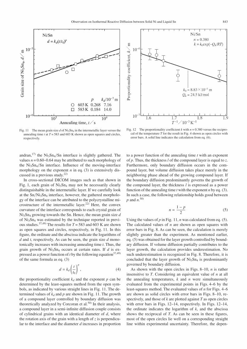
As shown with the open circles in Figs. 8–10, n is rather insensitive to T. Considering an equivalent value of n at all the annealing temperatures, k and n were simultaneously evaluated from the experimental points in Figs. 4–6 by the least-squares method. The evaluated values of n for Figs. 4–6 are shown as solid circles with error bars in Figs. 8–10, re-spectively, and those of k are plotted against T as open circles with error bars in Figs. 12–14, respectively. In Figs. 12–14, the ordinate indicates the logarithm of k, and the abscissa shows the reciprocal of T. As can be seen in these �gures, most of the open circles lie well on a corresponding straight line within experimental uncertainty. Therefore, the depen-
Fig. 11 The mean grain size d of Ni3Sn4 in the intermetallic layer versus the annealing time t at T = 583 and 603 K shown as open squares and circles, respectively.
Fig. 12 The proportionality coef�cient k with n = 0.380 versus the recipro-cal of the temperature T for the result in Fig. 4 shown as open circles with error bars. A solid line indicates the calculation from eq. (6).
843Observation on Isothermal Reactive Diffusion between Solid Ni and Liquid Sn

dence of k on T is expressed by the following equation.
k = k0 exp − Qk
RT (6)
Here, k0 is the pre-exponential factor, Qk is the activation en-thalpy, and R is the gas constant. The values of k0 and Qk were evaluated from the open circles by the least-squares method as shown with solid lines in Figs. 12–14. The evaluation pro-vides Qk = 24.5 kJ/mol, 18.7 kJ/mol and 15.7 kJ/mol for Figs. 12, 13 and 14, respectively. If the growth of the interme-tallic layer is purely controlled by volume diffusion and the
parabolic relationship holds between l and t, the dependence of k on T is estimated from the interdiffusion coef�cients and the solubility ranges of the constituent phases in the diffusion couple by an appropriate analytical technique.24–33) On the basis of the estimation, Qk is compared with the activation enthalpy of the interdiffusion coef�cient for each phase. However, n is typically smaller than 0.5 in Figs. 8 and 10 but greater than 0.5 in Fig. 9. Thus, unfortunately, the parabolic relationship does not hold between l and t. Consequently, the analytical technique24–33) cannot be used to estimate the value of Qk in a straightforward manner. When n is greater than 0.5, we may not determine whether boundary diffusion contrib-utes to the rate-controlling process. The value Qk = 24.5 kJ/mol with n = 0.38 and that Qk = 15.7 kJ/mol with n = 0.48 correlate with the compound growth controlled by boundary diffusion. If the compound growth for n = 0.63 is governed by volume diffusion, Qk should be much greater than 24.5 kJ/mol. However, the value Qk = 18.7 kJ/mol with n = 0.63 cor-responds to an intermediate value between Qk = 15.7 kJ/mol and 24.5 kJ/mol. From this intermediate value of Qk, it is concluded that boundary diffusion contributes to the com-pound growth not only at T = 523–623 K but also at T = 623–773 K.
4. Conclusions
To examine the kinetics of the reactive diffusion in the sol-id-Ni/liquid-Sn system, the Ni/Sn diffusion couples were prepared by the isothermal bonding technique and then im-mediately annealed at temperatures of T = 533–623 K. At these temperatures, Ni3Sn, Ni3Sn2 and Ni3Sn4 are the stable intermetallic compounds in the binary Ni–Sn system.23) During annealing, however, only Ni3Sn4 is formed as a visi-ble compound layer at the original Ni/Sn interface in the dif-fusion couple and grows mainly towards the liquid-Sn. The mean thickness of the compound layer increases in propor-tion to a power function of the annealing time. When volume diffusion controls the layer growth, the exponent n of the power function is equal to 0.5. If boundary diffusion contrib-utes to the rate-controlling process and grain growth occurs in the compound layer, however, n becomes smaller than 0.5. According to the observation, n takes values of 0.31–0.43 and grain growth actually takes place in the compound layer. This means that the layer growth is predominantly controlled by boundary diffusion.
Acknowledgements
The authors are grateful to Dr. Y. Nagatomo, Mr. T. Ohashi and Mr. K. Kuba at Mitsubishi Materials Co. Ltd., Japan for stimulating discussions. The present study was supported by Mitsubishi Materials Co. Ltd., Japan. The study was partially supported by a Grant-in-Aid for Scienti�c Research from the Ministry of Education, Culture, Sports, Science and Technol-ogy of Japan.
REFERENCES
1) L. Zakraysek: Welding Res. Suppl. Nov. (1972) 536–541. 2) K.N. Tu: Acta Metall. 21 (1973) 347–354.
Fig. 13 The proportionality coef�cient k with n = 0.627 versus the recipro-cal of the temperature T for the result in Fig. 5 shown as open circles with error bars. A solid line indicates the calculation from eq. (6).
Fig. 14 The proportionality coef�cient k with n = 0.478 versus the recipro-cal of the temperature T for the result in Fig. 6 shown as open circles with error bars. A solid line indicates the calculation from eq. (6).
844 A. Nakane, T. Suzuki, M. O and M. Kajihara

3) M. Onishi and H. Fujibuchi: Trans. JIM 16 (1975) 539–547. 4) H.N. Keller: IEEE Trans. Components Hybrids Manuf. Tech. CHMT-2
(1979) 180–195. 5) H.N. Keller and J.M. Morabito: Surf. Interface Anal. 3 (1981) 16–22. 6) J.O.G. Parent, D.D.L. Chung and I.M. Bernstein: J. Mater. Sci. 23
(1988) 2564–2572. 7) A.J. Sunwoo, J.W. Morris, Jr. and G.K. Lucey, Jr.: Metall. Trans. A 23
(1992) 1323–1332. 8) P.T. Vianco, P.F. Hlava and A.L. Kilgo: J. Electron. Mater. 23 (1994)
583–594. 9) D.R. Frear and P.T. Vianco: Metall. Trans. A 25 (1994) 1509–1523. 10) S. Choi, T.R. Bieler, J.P. Lucas and K.N. Subramanian: J. Electron.
Mater. 28 (1999) 1209–1215. 11) T. Takenaka, S. Kano, M. Kajihara, N. Kurokawa and K. Sakamoto:
Mater. Sci. Eng. A 396 (2005) 115–123. 12) C. Wright: IEEE Trans. Parts, Hybrids, Packaging PHP-13 (1977)
202–207. 13) H.N. Keller: IEEE Trans. Components, Hybrids, Manuf. Tech. CHMT-
5 (1982) 408–419. 14) E.I.-B. Hannech and C.R. Hall: Mater. Sci. Technol. 8 (1992) 817–824. 15) G. Ghosh: Acta Mater. 48 (2000) 3719–3738. 16) M. Mita, M. Kajihara, N. Kurokawa and K. Sakamoto: Mater. Sci. Eng.
A 403 (2005) 269–275. 17) S.K. Kang and V. Ramachandran: Scr. Metall. 14 (1980) 421–424. 18) C.-Y. Lin, C.-C. Jao, C. Lee and Y.-W. Yen: J. Alloy. Compd. 440
(2007) 333–340. 19) Y. Tanaka, M. Kajihara and Y. Watanabe: Mater. Sci. Eng. A 445–446
(2007) 355–363. 20) Y. Tanaka and M. Kajihara: Mater. Trans. 50 (2009) 2212–2220. 21) Y. Tanaka and M. Kajihara: J. Mater. Sci. 45 (2010) 5676–5684. 22) M. Hida and M. Kajihara: Mater. Trans. 53 (2012) 1240–1246. 23) T.B. Massalski, H. Okamoto, P.R. Subramanian and L. Kacprzak: Bina-
ry Alloy Phase Diagrams, vol. 3 (ASM International, Materials Park, OH, 1990) p. 2864.
24) M. Kajihara: Acta Mater. 52 (2004) 1193–1200.
25) M. Kajihara: Mater. Sci. Eng. A 403 (2005) 234–240. 26) M. Kajihara: Mater. Trans. 46 (2005) 2142–2149. 27) M. Kajihara: Diffus. Defect Forum 249 (2006) 91–96. 28) M. Kajihara: Mater. Trans. 47 (2006) 1480–1484. 29) Y. Tanaka and M. Kajihara: Mater. Trans. 47 (2006) 2480–2488. 30) M. Kajihara and T. Yamashina: J. Mater. Sci. 42 (2007) 2432–2442. 31) M. Kajihara: Mater. Trans. 49 (2008) 715–722. 32) M. Kajihara: Mater. Trans. 51 (2010) 1242–1248. 33) M. Kajihara: Mater. Trans. 53 (2012) 1896–1904. 34) T. Yamada, K. Miura and M. Kajihara: J. Mater. Sci. 39 (2004) 2327–
2334. 35) T. Yamada, K. Miura, M. Kajihara, N. Kurokawa and K. Sakamoto:
Mater. Sci. Eng. A 390 (2005) 118–126. 36) M. Mita, M. Kajihara, N. Kurokawa and K. Sakamoto: Mater. Sci. Eng.
A 403 (2005) 269–275. 37) T. Takenaka, M. Kajihara, N. Kurokawa and K. Sakamoto: Mater. Sci.
Eng. A 406 (2005) 134–141. 38) A. Furuto and M. Kajihara: Mater. Sci. Eng. A 445–446 (2007) 604–
610. 39) D. Naoi and M. Kajihara: Mater. Sci. Eng. A 459 (2007) 375–382. 40) M. Yamakami and M. Kajihara: Mater. Trans. 50 (2009) 130–137. 41) M. O and M. Kajihara: Mater. Trans. 52 (2011) 677–684. 42) M. O, Y. Takamatsu and M. Kajihara: Mater. Trans. 55 (2014) 1058–
1064. 43) A. Furuto and M. Kajihara: Mater. Trans. 49 (2008) 294–303. 44) A. Papapetrou: Z. Krist. 92 (1935) 89–129. 45) G.P. Ivantsov: Dokl. Akad. Nauk SSSR 58 (1947) 567–569. 46) G. Horvay and J.W. Cahn: Acta Metall. 9 (1961) 695–705. 47) R. Trivedi: Acta Metall. 18 (1970) 287–296. 48) P.E.J. Rivera-Diaz-del-Castillo and H.K.D.H. Bhadeshia: Mater. Sci.
Technol. 17 (2001) 25–29. 49) M. Hashiba, W. Shinmei and M. Kajihara: J. Electron. Mater. 41 (2012)
32–43. 50) Y.L. Corcoran, A.H. King, N. de Lanerolle and B. Kim: J. Electron.
Mater. 19 (1990) 1177–1183.
845Observation on Isothermal Reactive Diffusion between Solid Ni and Liquid Sn