
o¥¬ ïµ â - ir.nctu.edu.tw
93
國立交通大學 電子工程學系 電子研究所 碩 士 論 文 一個與電壓控制震盪器整合的 一個與電壓控制震盪器整合的 一個與電壓控制震盪器整合的 一個與電壓控制震盪器整合的 K 頻帶互補式金 頻帶互補式金 頻帶互補式金 頻帶互補式金 氧半 氧半 氧半 氧半 E 類功率放大器 類功率放大器 類功率放大器 類功率放大器 A K-Band CMOS Class E Power Amplifier Integrated with Voltage-Controlled Oscillator 研 究 生: 彭國權 (Guo-Quan Peng) 指導教授: 吳重雨教授 (Prof. Chung-Yu Wu) 中華民國九十九年十一月
Transcript of o¥¬ ïµ â - ir.nctu.edu.tw

國立交通大學
電子工程學系 電子研究所
碩 士 論 文
一個與電壓控制震盪器整合的一個與電壓控制震盪器整合的一個與電壓控制震盪器整合的一個與電壓控制震盪器整合的 K 頻帶互補式金頻帶互補式金頻帶互補式金頻帶互補式金
氧半氧半氧半氧半 E 類功率放大器類功率放大器類功率放大器類功率放大器
A K-Band CMOS Class E Power Amplifier
Integrated with Voltage-Controlled Oscillator
研 究 生: 彭國權 (Guo-Quan Peng)
指導教授: 吳重雨教授 (Prof. Chung-Yu Wu)
中華民國九十九年十一月

一個與電壓控制震盪器整合的一個與電壓控制震盪器整合的一個與電壓控制震盪器整合的一個與電壓控制震盪器整合的 K 頻帶互補式金氧半頻帶互補式金氧半頻帶互補式金氧半頻帶互補式金氧半
E 類功類功類功類功率放大器率放大器率放大器率放大器
A K-Band CMOS Class E Power Amplifier
Integrated with Voltage-Controlled Oscillator
研 究 生:彭國權 Student: Guo-Quan Peng
指導教授:吳重雨教授 Advisor: Prof. Chung-Yu Wu
國立交通大學
電子工程學系 電子研究所
碩士論文
A Thesis
Submitted to Department of Electronics Engineering and Institute of Electronics College of Electrical and Computer Engineering
National Chiao-Tung University in Partial Fulfillment of the Requirements
for the Degree of Master
in Electronics Engineering
November 2010
Hsin-Chu, Taiwan, Republic of China
中華民國九十九年十一月

i
一個與電壓控制震盪器整合的一個與電壓控制震盪器整合的一個與電壓控制震盪器整合的一個與電壓控制震盪器整合的 K頻帶互補頻帶互補頻帶互補頻帶互補
式金氧半式金氧半式金氧半式金氧半 E類功率放大器類功率放大器類功率放大器類功率放大器
研究生研究生研究生研究生: 彭國權彭國權彭國權彭國權
指導教授指導教授指導教授指導教授: 吳重雨吳重雨吳重雨吳重雨 博士博士博士博士
國立交通大學國立交通大學國立交通大學國立交通大學
電子工程學系電子工程學系電子工程學系電子工程學系 電子研究所碩士班電子研究所碩士班電子研究所碩士班電子研究所碩士班
摘要摘要摘要摘要
具有高操作頻具有高操作頻具有高操作頻具有高操作頻率高傳輸速率的通訊系統已被視為次世代通訊系統的主軸率高傳輸速率的通訊系統已被視為次世代通訊系統的主軸率高傳輸速率的通訊系統已被視為次世代通訊系統的主軸率高傳輸速率的通訊系統已被視為次世代通訊系統的主軸。。。。在最近在最近在最近在最近
幾年幾年幾年幾年,,,,K 頻帶頻帶頻帶頻帶中中中中,,,,已已已已有有有有許多頻帶如許多頻帶如許多頻帶如許多頻帶如 24.05–24.25-GHz的的的的 ISM-band 及及及及 22–29 GHz被被被被
FCC釋出作為汽車雷達應用等用途釋出作為汽車雷達應用等用途釋出作為汽車雷達應用等用途釋出作為汽車雷達應用等用途。。。。
此論文中介紹此論文中介紹此論文中介紹此論文中介紹實現一個實現一個實現一個實現一個與電壓控制震盪器整合與電壓控制震盪器整合與電壓控制震盪器整合與電壓控制震盪器整合操作在操作在操作在操作在K頻帶頻帶頻帶頻帶的的的的互補式金氧半互補式金氧半互補式金氧半互補式金氧半E類類類類
功率放大器功率放大器功率放大器功率放大器。。。。此此此此電路電路電路電路包含了包含了包含了包含了一個一個一個一個 LC 槽的電壓控制震盪器槽的電壓控制震盪器槽的電壓控制震盪器槽的電壓控制震盪器以及以及以及以及一個一個一個一個 E類類類類功率放功率放功率放功率放大器大器大器大器等等等等
電路並且使用了電路並且使用了電路並且使用了電路並且使用了 0.13-µµµµm CMOS技術來設計並製造技術來設計並製造技術來設計並製造技術來設計並製造。。。。藉由藉由藉由藉由使用使用使用使用電壓控制震盪器與高電壓控制震盪器與高電壓控制震盪器與高電壓控制震盪器與高功功功功
率率率率效益效益效益效益 E類功率放大器類功率放大器類功率放大器類功率放大器,,,,使得使得使得使得在在在在大訊號操作大訊號操作大訊號操作大訊號操作高輸出功率高輸出功率高輸出功率高輸出功率的傳送器電路的傳送器電路的傳送器電路的傳送器電路上上上上可以得到高可以得到高可以得到高可以得到高功功功功
率效益率效益率效益率效益的性能的性能的性能的性能。。。。
此電路包含了此電路包含了此電路包含了此電路包含了電壓控制震盪器電壓控制震盪器電壓控制震盪器電壓控制震盪器以及以及以及以及 E類類類類功率放大器等電路功率放大器等電路功率放大器等電路功率放大器等電路,已被模擬已被模擬已被模擬已被模擬、、、、實現實現實現實現於於於於 1.05
mm2 的晶片面積的晶片面積的晶片面積的晶片面積、、、、以及量測以及量測以及量測以及量測。。。。根據量測結果根據量測結果根據量測結果根據量測結果,,,,此電路由於佈局時此電路由於佈局時此電路由於佈局時此電路由於佈局時的錯誤的錯誤的錯誤的錯誤、、、、EM、、、、寄生寄生寄生寄生
效應效應效應效應的的的的考慮考慮考慮考慮沒有詳盡沒有詳盡沒有詳盡沒有詳盡,,,,使得使得使得使得輸出功率減少輸出功率減少輸出功率減少輸出功率減少 12.56 dB。。。。然而然而然而然而,,,,從修改後的模擬結果從修改後的模擬結果從修改後的模擬結果從修改後的模擬結果與其與其與其與其
它所發表它所發表它所發表它所發表電路電路電路電路比較比較比較比較可知可知可知可知,,,,此電路操作在此電路操作在此電路操作在此電路操作在較低較低較低較低的供應的供應的供應的供應電壓下電壓下電壓下電壓下,,,,仍有較仍有較仍有較仍有較高高高高的的的的功率效益功率效益功率效益功率效益。。。。因因因因
此此此此,,,,E 類功率放大器類功率放大器類功率放大器類功率放大器電路電路電路電路非常適合用在非常適合用在非常適合用在非常適合用在高功率效益的應用高功率效益的應用高功率效益的應用高功率效益的應用,,,,尤其是高整合度尤其是高整合度尤其是高整合度尤其是高整合度、、、、低成本低成本低成本低成本
的的的的 CMOS製程製程製程製程。。。。

ii
A K-Band CMOS Class E Power Amplifier
Integrated with Voltage-Controlled
Oscillator
Student: Guo-Quan Peng Advisor: Dr. Chung-Yu Wu
Department of Electronic Engineering &
Institute of Electronics
National Chiao Tung University
Abstract
In the next-generation wireless communication, high data rate transmission with a high
operating frequency is expected to be realized. Over the past few years, the
24.05–24.25-GHz Industrial, Scientific, and Medical (ISM) band, 22–29 GHz band
provided by Federal Communications Commission (FCC) for the operation of vehicular
radar have been released.
In this thesis, a K-band CMOS class E power amplifier integrated with
voltage-controlled oscillator is presented. The proposed circuits which consist of a LC-tank
voltage-controlled oscillator and a class E power amplifier are designed using 0.13-µm
CMOS technology. By adopting voltage-controlled oscillator and high efficiency class E
power amplifier, the large-signal operated high output power transmitter circuit can be
implemented with high efficiency performance.
The proposed circuits, including a voltage-controlled oscillator and a class E power

iii
amplifier, are simulated, fabricated with a chip size of 1.05 mm2, and measured. Because of
the layout mistake, and the effects such as EM, parasitic effect which are not carefully
considered before fabrication, the measured output power decreases 12.56 dB. Comparing
the results of the re-design circuits with other proposed circuits, however, the class E power
amplifier can have better efficiency under lower supply voltage. Therefore, class E power
amplifier is suitable for high efficiency application, especially for high-integrated low-cost
CMOS technology.

iv
誌誌誌誌 謝謝謝謝
本論文能夠順利完成本論文能夠順利完成本論文能夠順利完成本論文能夠順利完成,,,,首先要感謝的是我的論文指導教授吳重雨老師這幾年首先要感謝的是我的論文指導教授吳重雨老師這幾年首先要感謝的是我的論文指導教授吳重雨老師這幾年首先要感謝的是我的論文指導教授吳重雨老師這幾年
下來辛勤的指導下來辛勤的指導下來辛勤的指導下來辛勤的指導。。。。在老師的教誨下在老師的教誨下在老師的教誨下在老師的教誨下,,,,讓我學到很多類比積體電路設計的專業知識讓我學到很多類比積體電路設計的專業知識讓我學到很多類比積體電路設計的專業知識讓我學到很多類比積體電路設計的專業知識
和待人處世的方法和待人處世的方法和待人處世的方法和待人處世的方法,,,,使我受益匪淺使我受益匪淺使我受益匪淺使我受益匪淺。。。。
另外要感謝博士班的王文傑學長另外要感謝博士班的王文傑學長另外要感謝博士班的王文傑學長另外要感謝博士班的王文傑學長、、、、黃祖德學長黃祖德學長黃祖德學長黃祖德學長、、、、陳旻珓學長陳旻珓學長陳旻珓學長陳旻珓學長、、、、虞繼堯學長虞繼堯學長虞繼堯學長虞繼堯學長、、、、
蘇煊毅學長蘇煊毅學長蘇煊毅學長蘇煊毅學長、、、、Fadi 學長學長學長學長、、、、台祐學長台祐學長台祐學長台祐學長、、、、世豪學長世豪學長世豪學長世豪學長等曾經給我的指點等曾經給我的指點等曾經給我的指點等曾經給我的指點、、、、討論和協助討論和協助討論和協助討論和協助,,,,
讓我在研究的過程中能順利的進行讓我在研究的過程中能順利的進行讓我在研究的過程中能順利的進行讓我在研究的過程中能順利的進行。。。。再來我要感謝碩班已畢業的學長們以及實驗再來我要感謝碩班已畢業的學長們以及實驗再來我要感謝碩班已畢業的學長們以及實驗再來我要感謝碩班已畢業的學長們以及實驗
室的同學與學弟妹們室的同學與學弟妹們室的同學與學弟妹們室的同學與學弟妹們::::順維學長順維學長順維學長順維學長、、、、國忠學長國忠學長國忠學長國忠學長、、、、維德學長維德學長維德學長維德學長、、、、柏宏學長柏宏學長柏宏學長柏宏學長、、、、廷偉學長廷偉學長廷偉學長廷偉學長、、、、
晏維學長晏維學長晏維學長晏維學長、、、、昌平學長昌平學長昌平學長昌平學長、、、、大仔大仔大仔大仔、、、、塔哥塔哥塔哥塔哥、、、、區文區文區文區文、、、、威宇威宇威宇威宇、、、、政邦政邦政邦政邦、、、、建名建名建名建名、、、、歐陽歐陽歐陽歐陽、、、、科科科科科科科科、、、、紹紹紹紹
歧歧歧歧、、、、北鴨北鴨北鴨北鴨、、、、世範世範世範世範、、、、宗恩宗恩宗恩宗恩、、、、亭州亭州亭州亭州、、、、順天學弟順天學弟順天學弟順天學弟、、、、育祥學弟育祥學弟育祥學弟育祥學弟、、、、kittykittykittykitty 學弟學弟學弟學弟、、、、敬程學弟敬程學弟敬程學弟敬程學弟、、、、
韋丞學弟韋丞學弟韋丞學弟韋丞學弟、、、、宗昀學弟宗昀學弟宗昀學弟宗昀學弟、、、、慧君學妹慧君學妹慧君學妹慧君學妹、、、、慧雯學妹慧雯學妹慧雯學妹慧雯學妹、、、、世昕學弟世昕學弟世昕學弟世昕學弟、、、、邱神學弟邱神學弟邱神學弟邱神學弟、、、、佳琪學妹佳琪學妹佳琪學妹佳琪學妹、、、、
堂龍學弟堂龍學弟堂龍學弟堂龍學弟、、、、書瑾學妹書瑾學妹書瑾學妹書瑾學妹、、、、子薰學弟子薰學弟子薰學弟子薰學弟、、、、明翰學弟明翰學弟明翰學弟明翰學弟、、、、、、、、、、、、等等等等。。。。在這幾年中我們一起研究在這幾年中我們一起研究在這幾年中我們一起研究在這幾年中我們一起研究
功課功課功課功課,,,,在失落的時候互相鼓勵在失落的時候互相鼓勵在失落的時候互相鼓勵在失落的時候互相鼓勵,,,,使我在碩士生涯不會有孤單奮戰的感覺使我在碩士生涯不會有孤單奮戰的感覺使我在碩士生涯不會有孤單奮戰的感覺使我在碩士生涯不會有孤單奮戰的感覺。。。。
另外另外另外另外,,,,我要謝謝我的女朋友佐芝我要謝謝我的女朋友佐芝我要謝謝我的女朋友佐芝我要謝謝我的女朋友佐芝,,,,謝謝妳陪我走過我的碩士生涯謝謝妳陪我走過我的碩士生涯謝謝妳陪我走過我的碩士生涯謝謝妳陪我走過我的碩士生涯,,,,在我最失在我最失在我最失在我最失
落失意的時候落失意的時候落失意的時候落失意的時候,,,,能忍受我的脾氣並鼓勵能忍受我的脾氣並鼓勵能忍受我的脾氣並鼓勵能忍受我的脾氣並鼓勵、、、、接受接受接受接受著著著著我我我我。。。。
最後最後最後最後,,,,我要謝謝我的家人我要謝謝我的家人我要謝謝我的家人我要謝謝我的家人,,,,謝謝你們無限制的容忍著我的失敗與失落謝謝你們無限制的容忍著我的失敗與失落謝謝你們無限制的容忍著我的失敗與失落謝謝你們無限制的容忍著我的失敗與失落,,,,讓我讓我讓我讓我
感受到無論發生什麼事都有人支持著我感受到無論發生什麼事都有人支持著我感受到無論發生什麼事都有人支持著我感受到無論發生什麼事都有人支持著我,,,,而使我能無後顧之憂的向成功邁進而使我能無後顧之憂的向成功邁進而使我能無後顧之憂的向成功邁進而使我能無後顧之憂的向成功邁進。。。。
其他要感謝的人還有很多其他要感謝的人還有很多其他要感謝的人還有很多其他要感謝的人還有很多,,,,無法一一列出無法一一列出無法一一列出無法一一列出,,,,在此一併謝過在此一併謝過在此一併謝過在此一併謝過。。。。
彭國權彭國權彭國權彭國權
于于于于 風城交大風城交大風城交大風城交大
99999999 年年年年 冬冬冬冬

v
A K-Band CMOS Class E Power Amplifier Integrated with
Voltage-Controlled Oscillator
Contents
Chinese Abstract i English Abstract ii Acknowledgement iv Contents v Table Captions vii Figure Captions viii Chapter 1 Introduction 1.1 Background 1 1.1.1 Review on Class E Power Amplifier
1.1.2 Review on K-Band (18 - 26.5 GHz) Power
Amplifier
2
5
1.2 Motivation 10 1.3 Main Results and Thesis Organization 12 Chapter 2 Circuit Design and Simulation Results 2.1 Design Considerations 14 2.2 Circuit Design 16 2.2.1 Class E Power Amplifier 16
2.2.2 Voltage-Controlled Oscillator with Cascode
Buffer
36
2.2.3 Class E Power Amplifier Integrated with
Voltage-Controlled Oscillator
39
2.3 Post-Simulation Results 44 Chapter 3 Experimental Results 3.1 Chip Layout Descriptions 54 3.2 Measurement Setup 56 3.3 Experimental Results 56 3.4 Discussion 62 3.4.1 The Degradation of Output Power
3.4.2 The Degradation of Frequency Drift
62
63

vi
3.4.3 Revised Post-Simulation Results 64
3.5 Re-Design 69 Chapter 4 Conclusions and Future Work 4.1 Conclusions 77 4.2 Future Work 79 References 80

vii
Table Captions Table 1-1 Performance of the class of power amplifiers at K-band 11
Table 2-1 Summary of device value 42
Table 2-2 Dimension summary of transmission line 43
Table 2-3 Summaries of original post-sim results1 53
Table 2-4 Summaries of original post-sim results2 53
Table 3-1 Summaries of measurement results 61
Table 3-2 Summaries of revised post-sim results 68
Table 3-3 Dimensions summaries of the re-design version 70
Table 3-4 Comparison with other K-band power amplifiers 74
Table 3-5 Comparison with other K-band power amplifiers 74
Table 3-6 Summaries of re-design post-sim results 75
Table 3-7 Ron case comparisons 76

viii
Figure Captions Fig. 1-1 24-GHz service band plan release by FCC 1
Fig. 1-2 Class E power amplifier 3
Fig. 1-3 Drain voltage and current waveforms of ideal class E power
amplifier
3
Fig. 1-4 Schematic of proposed class E power amplifier in [9] 5
Fig. 1-5 Schematic of proposed current-mode power amplifier in [10] 5
Fig. 1-6 Schematic of proposed K-band power amplifier in [11] 6
Fig. 1-7 Schematic of proposed 24 GHz power amplifier in [12] 8
Fig. 1-8 Schematic of proposed 24 GHz power amplifier in [13] 9
Fig. 2-1 Block diagrams of polar loop structure 15
Fig. 2-2 The load network of class E power amplifier 17
Fig. 2-3 Voltage and current waveforms of class E power amplifier 17
Fig. 2-4 Response of class E power amplifier when the transistor turns off 18
Fig. 2-5 Effect for optimal load when swing is limited 19
Fig. 2-6 Optimal load resistance determined by load-line analysis 20
Fig. 2-7 Neutralization for resonating parasitic Cgd 22
Fig. 2-8 Small-signal model of common-source transistor 22
Fig. 2-9 Equivalent network between gate-drain of common-source
transistor
25
Fig. 2-10 Equivalent network between gate-drain of common-source
transistor (L’ gd is the combination of Lgd and Cb)
25
Fig. 2-11 The load network of ideal case class E power amplifier 26
Fig. 2-12 The load network of Ron case class E power amplifier 28
Fig. 2-13 Schematic of designed power amplifier 31
Fig. 2-14 Stability factor (k factor) 33
Fig. 2-15 Stability means (b factor) 33
Fig. 2-16 Constant Pout, constant PAE contours and the chosen ZL 35
Fig. 2-17 Impedance transformation network of power amplifier 35
Fig. 2-18 Load impedance transferred by transformation network 36
Fig. 2-19 The design of LC-tank VCO 37

ix
Fig. 2-20 The design of voltage-controlled oscillator with cascode buffer 39
Fig. 2-21 Schematic of designed whole circuits 41
Fig. 2-22 Schematic of designed whole circuits (with parasitic routing effect) 41
Fig. 2-23 Layout, 3-D model and setting for EM analysis (2-port networks) 41
Fig. 2-24 With and without neutralization technique analysis of re-matching
stand-alone class E power amplifier
45
Fig. 2-25 Neutralization technique phase shift of re-matching stand-alone
class E power amplifier
46
Fig. 2-26 Neutralization technique phase shift effect 46
Fig. 2-27 Drain voltage and current waveforms with gate voltage waveform
of re-matching stand-alone class E power amplifier
47
Fig. 2-28 Large signal S-parameter (LSSP) for re-matching stand-alone
class E power amplifier
47
Fig. 2-29 Pout vs Pin, PAE vs Pin and Drain Efficiency vs Pin for re-matching
stand-alone class E power amplifier
48
Fig. 2-30 Tuning range of voltage-controlled oscillator 49
Fig. 2-31 Phase noise of voltage-controlled oscillator 49
Fig. 2-32 Pout vs Vtune for whole circuits 50
Fig. 2-33 Overall drain Efficiency vs Vtune for whole circuits 51
Fig. 2-34 Output power spectrum for whole circuits 51
Fig. 2-35 Pout vs Pin, PAE vs Pin and Drain Efficiency vs Pin for cascode
buffer with power amplifier
52
Fig. 3-1 Chip microphotograph of the proposed whole circuits 55
Fig. 3-2 Measurement setup for the proposed whole circuits 56
Fig. 3-3 Measured output frequency v.s. tuning voltage for proposed whole
circuits
58
Fig. 3-4 Measured output power v.s. tuning voltage for proposed whole
circuits
58
Fig. 3-5 Measured phase noise for proposed whole circuits 59
Fig. 3-6 Measured output power spectrum for proposed whole circuits 59
Fig. 3-7 Pout vs Pin for cascode buffer with power amplifier 60
Fig. 3-8 PAE and drain efficiency vs Pin for cascode buffer with power 60

x
amplifier
Fig. 3-9 The crossover MOS line and the effect in the gate waveforms of
Mbuffer4
63
Fig. 3-10 Layout view and 3-D model in HFSS for revised post-simulation 64
Fig. 3-11 Output frequency of revised post-sim comparing with original
post-sim and measurement
65
Fig. 3-12 Output power of revised post-sim comparing with original
post-sim and measurement
65
Fig. 3-13 Phase noise of revised post-sim comparing with original post-sim 66
Fig. 3-14 Pout vs Pin of revised post-sim comparing with original post-sim
and measurement
66
Fig. 3-15 PAE and drain efficiency vs Pin of revised post-sim comparing with
original post-sim and measurement
67
Fig. 3-16 Change components’ dimensions for re-design 70
Fig. 3-17 The modified layout for re-design whole circuits 71
Fig. 3-18 Output frequency of re-design comparing with original and
revised post-sim
71
Fig. 3-19 Output power of re-design comparing with original and revised
post-sim
72
Fig. 3-20 Phase noise of re-design comparing with original and revised
post-sim
72
Fig. 3-21 Pout vs Pin of re-design comparing with original and revised
post-sim
73
Fig. 3-22 PAE and drain efficiency vs Pin of re-design comparing with
original and revised post-sim
73

1
Chapter 1
Introduction
1.1. Background
Recently, the research on radio-frequency integrated circuits (RFICs) in higher
frequencies have been accelerated since the frequency spectra below 10 GHz have
gradually become crowded by massive requirements of data transmission from the
modern wireless applications such as Bluetooth, wireless local area network (WLAN)
and ultra-wideband (UWB), etc. Many researchers investigate RF transceiver front-end
circuits in 24 GHz because higher operating frequency can provide more bandwidth. In
addition, the 24.05–24.25-GHz Industrial, Scientific, and Medical (ISM) band [1],
22–29 GHz band provided by Federal Communications Commission (FCC) for the
operation of vehicular radar [2]–[3], and the 24-GHz band plan as shown in Fig. 1-1 [4]
are released.
Fig. 1-1 24-GHz service band plan release by FCC

2
In RF transmitter front-end, key components such as voltage-controlled
oscillators (VCOs) and power amplifiers (PAs) have been reported in many CMOS
designs [5]–[7]. Nevertheless, in standard CMOS technologies, the active devices have
poor inherent characteristics comparing to GaAs and SiGe, and the passive
components such as planar inductors have higher losses from lossy substrate. These
inherent characteristics seriously degrade the performance of the transmitter front-end
circuits. However, today’s consumers demand wireless systems that are low-cost,
power efficient, reliable and have a high integration form. High levels of integration
are desired to reduce cost and achieve compact form. Hence the long term vision of
goal for wireless transceiver is to merge as many components as possible to a single
die in an inexpensive technology. Therefore, there is a growing interest in utilizing
CMOS technologies for RF power amplifier (PAs) [8]. Although the output power of
the transmitter can be increased by utilizing multiple parallel transistors to implement
power amplifiers [5], the power-added efficiency (PAE) remains the same in such a
structure. To improve the PAE, several design techniques have been proposed. By
using the special structure of transmission line and additional algorithms, the PAE of a
RF CMOS PA can be improved to around 10% [6]–[7].
1.1.1. Review on Class E Power Amplifier
Class E power amplifier is a single transistor operated as a switch. It uses a high
order reactive network to shape the switch voltage to have both zero value (zero
voltage switching; ZVS) and slope (zero derivative switching; ZDS) at the switch
turn-on. Therefore, the ideal efficiency is 100 %. A class E power amplifier is showed
in Fig. 1-2. The drain voltage and current waveform of ideal class E power amplifier is
showed in Fig. 1-3.

3
VinMpa
Vdd,pa
RFC
Cshunt RL
Lshaping
Cshaping
Vout
Vc
Id
Fig. 1-2 Class E power amplifier
Fig. 1-3 Drain voltage and current waveforms of ideal class E power amplifier

4
Obviously, the current of the transistor is near maximum when the switch turns
off. However, it will introduce a significant switch turn off losses because the switch is
not infinitely fast. Hence, it will reduce the efficiency. Another drawback is the large
peak voltage approximately 3.56 Vdd,pa when the switch sustains in the off state.
Therefore, it needs a high breakdown voltage and is not a good choice for
short-channel devices.
An 18 GHz fully-integrated class E power amplifier is proposed in [9], as shown
in Fig. 1-4. It consists of a two-stage cascode amplifier, a common source driver, and
an output stage. Due to the limited voltage headroom, common-source amplifiers are
used in the last two stages. The cascode amplifiers are used to provide sufficient gain,
good input matching and isolation from the last two stages which potentially could
oscillate. Besides, this proposed fully-integrated class E power amplifier also adopts a
mode-locking (also known as injection-locking) technique exploiting the instability of
driver amplifier which is used to improve the drive for the gate of output stage. The
mode-locking technique actually increases the gain of the circuit and reduces the drive
requirement for switching the output transistor. The comparison table in [9] shows that
this class E power amplifier has significantly higher efficiency and lower input
requirement than that for the previously reported CMOS PA operating near 20 GHz. It
also suggests CMOS technology is a viable candidate for building fully-integrated
transmitter near 20 GHz. But the method of its isolation is too complicated; we
develop another kind of isolation technique to improve this disadvantage as will be
discussed after. Due to the limited voltage headroom, the power supply of [9] is too
high and the power added efficiency (PAE) is not high enough.

5
Fig. 1-4 Schematic of proposed class E power amplifier in [9]
1.1.2. Review on K-Band (18 - 26.5 GHz) Power Amplifier
Schematic shown in Fig. 1-5 is a 24 GHz current-mode power amplifier proposed
in [10]. It is accomplished by using two-stage cascade current-mirror structure and it
also operates in class AB mode. Besides, the proposed current-mode power amplifier
also uses L7 and L8 to resonate the device capacitance between gate and drain of M8
and M10. It also uses R3 for low frequency stability consideration. And the optimized
output impedance transfer network is determined by the load-pull simulation. From the
comparison table in [10], it shows that the proposed CMOS current-mode power
amplifier has the highest PAE and the largest output power among the RF PAs.
Fig. 1-5 Schematic of proposed current-mode power amplifier in [10]
Schematic shown in Fig. 1-6 is another K-band power amplifier proposed in [11].
It is composed of 3 stages. The first two stages are driver stage, and the third stage is

6
formed by two parallel power cells. The typical topologies of the CMOS transistors are
common source and cascode. The biasing point of this design is at class A for better
linearity. The devices selected in the power cell were determined by the load-pull
simulation from the large signal model provided by TSMC, and the Gmax simulation.
The power stage includes two power cells. And the power cells are in-phase combined
directly. Two odd-mode suppression resistors of 11 Ω are placed within two power
cells for stability consideration. Each power cell was pre-matched to 100 Ω by an
appropriate matching network before binary combining. The matching network
includes an inductor (used for inductive peaking), and impedance transform network,
which is implemented by thin film micro-strip lines (TFMS) used for lower loss than
lumped elements for wide band power match. Appropriate bypass circuits are placed at
each bias point for low frequency stability consideration. The comparison table in [11]
shows that the proposed K-band power amplifier has the highest gain and good output
power in standard CMOS process.
Fig. 1-6 Schematic of proposed K-band power amplifier in [11]

7
Schematic shown in Fig. 1-7 is a 24 GHz power amplifier proposed in [12]. By
shunt combining N times transistors with device size of (W/N), the parasitic
capacitance Cgd of each transistor is reduced, which means higher gain and output
power performance are maintained. The binary combining method is a simple way to
combine output power of each transistor with equal phase and loss. To maintain low
loss in output matching circuits with good stability at low frequency, output high pass
matching network is chosen. A shunt short stub is connected to the device to resonance
the parasitic capacitance and provides dc biasing path. By shunting the resonance stubs,
the optimum load impedance is calculated via the load line estimation and the load-pull
simulation. The T-shaped high-pass matching is used as impedance transformer and
ensures the low frequency stability. In order to achieve higher gain and better linearity
performance, the cascode pairs are all biased in class A. It also uses thin-film
micro-strip line (TFMS) for interconnection and matching stubs. The proposed 24 GHz
power amplifier provides larger gain and power compared to commercial designs.
From the comparison table in [12], the proposed power amplifier shows the highest
OP1dB and saturation power among the CMOS PAs above 20 GHz.

8
VDD
VDD
32 fingers
160 m width
Binary
combination
T-matching
Ropt 25 Ω
RFin
50 ohm
RFout
50 ohm
Thin Film Micro-Strip Line
(TFMS)
Fig. 1-7 Schematic of proposed 24 GHz power amplifier in [12]
Schematic shown in Fig. 1-8 is a 24 GHz power amplifier proposed in [13]. The
PA has two gain stages with each gain stage consisting of a cascode transistor pair to
ensure stability and increase breakdown voltage. The PA is designed to operate in class
AB mode. The output and inter-stage matching networks in the PA are realized with
the substrate-shielded coplanar waveguide structure to reduce power losses and area.
The substrate-shielded coplanar waveguide is leading to more than a factor of two
reductions in wavelength at 24 GHz when compared to a standard coplanar waveguide
structure in silicon dioxide. The short wavelengths can improve isolation and make this
structure particularly suitable for integrating multiple power amplifiers on the same die.
Amplifier stability is improved by the RC network at the input of each stage, which
guarantees low frequency stability.

9
Fig. 1-8 Schematic of proposed 24 GHz power amplifier in [13]

10
1.2. Motivation
This research focuses on the novel approach for designing and implementing
24-GHz transmitter circuits by CMOS technology.
Because of the applications released in 24-GHz frequency range, many
researchers are attracted to design high-performance and low-cost wireless
applications in this frequency band with advanced CMOS technologies. However,
CMOS technology has limitation of low supply voltage. That is why traditional
commercial implementation of wireless transceivers typically utilizes a mixture of
technologies in order to implement a high-performance, completed system.
Nevertheless, considering the cost and integration capability, CMOS technology is
still the most suitable choice for designing RF circuits.
When implementing 24-GHz transmitter circuits by CMOS technology, the
output power of the transmitter can be increased by utilizing some structures to
implement power amplifiers. The higher output power can be achieved, but the
power-added efficiency remains the same in such structures. Therefore, the
improvement of the PAE of a RF CMOS PA at the higher output power level is a main
course of discussion. According to theses reasons as mentioned above, the class E
power amplifier compared with other class of power amplifiers at K-band as the Table
1-1 shown can provide higher power-added efficiency. Therefore, at 24-GHz, we
adopt the class E power amplifier as our design which tries to improve the PAE of a
RF CMOS PA at the higher output power level and use the voltage-controlled
oscillator as the input signal of class E power amplifier. The use of class E power
amplifier has solved the design conflict between improvement of power efficiency
and maintenance of amplifier linearity in K-band system. Besides, in order to solve
the isolation problem, a neutralization technique must be developed.

11
[9] *[10] [11] [12] [13]
Technology 0.13-µm CMOS 0.13-µm CMOS 0.18-µm CMOS 0.18-µm CMOS 0.18-µm CMOS
Topology Class E Class AB Class A Class A Class AB
Supply Voltage (V) 1.5 1.2 3.6 3.6 2.5
Freq (GHz) 18 20 24 18-23 24 24
Output Power
(dBm) 10.9 10.2 17.1 20.1 22 14
Peak PAE (%) 23.5 20.5 23.9 9.3 20 6.5
Chip Area (mm2) 0.782 1.05 2.4 0.42 14.28
*[10] : redesign post-sim results of proposed power amplifier in [10]
Table 1-1 Performance of the class of power amplifiers at K-band

12
1.3 . Main Results and Thesis Organization
In this work, the voltage-controlled oscillator and class E power amplifier are
designed. The voltage-controlled oscillator is realized by cross-coupled NMOS with
LC tank and PMOS current source oscillator. Besides, the voltage-controlled oscillator
cascades with a cascode buffer. A differential single stage common source class E
amplifier is proposed for the power amplifier. This is the first work including a
voltage-controlled oscillator and a power amplifier for K-band applications.
Measurement results show that the measured output center frequency and maximum
output power are 23.2 GHz and –2.41 dBm, respectively. The measured phase noise is
-108 dBc at 10 MHz. The measured output power of cascode buffer with power
amplifier is lower than original post layout simulation about 13 dB. And the measured
total power consumption of VCO and power amplifier is 29.4 mW from 1.2 V power
supply. From the analysis, experimental results, and re-design circuit, the proposed
circuit is suitable for high efficiency application.
The post layout simulation results of the re-design circuits show that the output
center frequency and maximum output power are 24.26 GHz and 10.41 dBm,
respectively. The phase noise is -119.9 dBc at 10 MHz. The output power of cascode
buffer with power amplifier is almost the same to the original post layout simulation.
And the total power consumption of VCO and power amplifier is 56.13 mW from 1.2
V power supply. The power consumption is less than other type power amplifier
because the class E power amplifier operates at the threshold voltage.
The thesis is divided into five chapters. Chapter 1 introduces the background,
motivation and main results of this research. The whole circuit design and simulation
results of this thesis will be presented at Chapter 2. Design considerations are
discussed in Section 2.1. Then the power amplifier, voltage-controlled oscillator and

13
the whole circuits design procedures are presented in Section 2.2.1, 2.2.2, and 2.2.3,
respectively. Post-simulation results are shown in Section 2.3.
The chip microphotograph, measurement setup, experimental results, revised post
simulation and re-design will be included in Chapter 3. Finally, the conclusions and
future work will be presented in Chapter 4.

14
Chapter 2
Circuit Design and Simulation Results
2.1. Design Considerations
How to use CMOS technology to design large-signal transmitter front-end
circuits is the most challenge part. In order to obtain enough trans-conductance, the
transistors’ sizes must be increased. However, the larger the size it is, the more serious
parasitic effect it will be. The parasitic capacitance effect will provide leakage path for
high-frequency signal or degrade reverse isolation and stability. In this research, these
leakage paths for RF signal and stability-degraded effects are resonated and
neutralized by on-chip inductors, respectively. The output matching network of power
amplifier is determined by load-pull analysis which considers the imaginary part
caused by the parasitic effect.
The block diagrams of polar loop structure are shown in Fig. 2-1. In this research,
as shown in Fig. 2-1, the proposed circuits included a voltage-controlled oscillator
with cascode buffer and a class E power amplifier are realized with 0.13-µm standard
CMOS technology. The designed VCO is implemented by the cross-coupled NMOS
with LC tank concept in order to provide a signal source for class E power amplifier.
The class E power amplifier is also realized by push-pull concept. The 1st-stage of
cascode buffer the RF signal comes from designed VCO to drive the 2nd-stage of class
E power amplifier. The 2nd-Stage is designed to have capability to provide enough
signal swing that the required output power can be achieved. The specification of the
designed whole circuits is to output more than 10-dBm output power at 24 GHz.

15
Limiter
LO2_Q
LO2_I
Fig. 2-1 Block diagrams of polar loop structure

16
2.2. Circuit Design
2.2.1. Class E Power Amplifier
Class E power amplifiers (PA) have been proved to be popular radio frequency
(RF) PAs with high efficiency. Using Class E power amplifier can maintain high
enough efficiency at high output power level. To achieve high enough efficiency, the
output load network must be carefully designed to eliminate the overlap between
voltage and current waveform at the designated operating frequency and output power
level. Generally speaking, the transistor output capacitance included the parasitic
capacitances constructs an optimum parallel reactance at the output load network and
satisfies the optimum Class E power amplifier conditions. The conditions of Class E
power amplifier were given by Sokal [14], and can be put in the form:
( ) 0
E (2.1)0
on
sw on
sw
t
v t
Class dv
dt
=⇔ =
Where ton represents the instant at which the switch closes, and vsw(t) represents the
switch voltage. These conditions can be guaranteed by the use of the load network
shown in Fig. 2-2. And the voltage and current waveforms of Class E power amplifier
are also shown in Fig. 2-3. Above equations show the typical properties of Class E
power amplifiers, where the passive components are used to minimize the
drain-source voltage when the switch closes. This property of Class E power
amplifiers is usually called “zero voltage switching”. Furthermore, another one
property can demand that the derivative of the switch voltage also equals zero at the
switching moment. Which is usually called “zero derivative switching”. These
demands will make the amplifier less sensitive to timing errors and component
variations [15].

17
Fig. 2-2 The load network of class E power amplifier
Fig. 2-3 Voltage and current waveforms of class E power amplifier

18
After the switch turns off, the load network operates as a damped second-order
system as shown in Fig. 2-4 with initial conditions across Cp and Cs and in Ls. The
time response depends on the quality factor Q of the network for underdamped,
overdamped, and critically damped conditions. We note that in the last case, VX
approaches zero volt with zero slope.
Fig. 2-4 Response of class E power amplifier when the transistor turns off
When implementing a power amplifier at high output power level, the most
critical node in the power amplifier circuit is its output node and resultant large
voltage and current swing are required. Operated at high output power level which
implies to need large DC bias means that the reliability such as metal current density
must be considered. Besides, large voltage and current swing which implies to the
large-signal operation viewpoint must also be considered with the small-signal
operation viewpoint at the same time. Therefore, for the power amplifiers of RF
systems, the output impedance transformation networks (output matching networks)
are always implemented by load-line or load-pull analysis method instead of
traditional conjugate matching analysis method.
The traditional conjugate matching analysis method can provide maximal power
transfer only under the condition of no current and voltage swing limitation. In other
words, it is always true for small-signal operation. That’s why most of RF systems,
such as receiver, adopt traditional conjugate matching analysis method for their
matching networks. However, in the transmitter front-end, especially for the output of
power amplifier, the large voltage and current swing are large signal operation

19
viewpoints. Because the output of power amplifier always produces high output
power level, the current or voltage swing always reaches the limitation of its supply.
Therefore, the output matching networks of power amplifiers are usually determined
by two methods – load-line or load-pull analysis methods instead of traditional
conjugate matching analysis method.
Fig. 2-5 shows the quantitative description of the above analysis methods for the
difference of optimal load if the voltage and current swing are limited. For traditional
conjugate matching analysis method, the load resistance RLOAD is chosen to equal to
RS. Under the voltage and current swing are limited conditions, the “VMAX /IMAX ” load
resistance has maximal output power delivered capability than any other load
resistance.
Fig. 2-5 Effect for optimal load when swing is limited
The hand-calculated procedure for load-line analysis can be accessed through
(2.2)–(2.3).
, DC knee DC= ( - ) (2.2)OUT MAX
1P V V I
2
,
-= (2.3)DC knee
L OPTDC
V VR
I
According to these equations, the load-line analysis on a common-source
transistor I-V curve is illustrated in Fig. 2-6.

20
RL>RL,OPT(lower current swing)
Vknee VDC VMAXVDS
ID
IMAX
IDC
RL=RL,OPT
RL<RL,OPT(lower voltage swing)
Fig. 2-6 Optimal load resistance determined by load-line analysis
The black color load-line is the optimal load resistance determined by load-line
analysis. And the optimal load resistance value also equals “VMAX /IMAX ”. It shows that
the black color load-line has maximal output power under this voltage and current
swing limitation. The red color load-line is the load resistance which is smaller than
the optimal resistance. It will have the same current swing but smaller voltage swing
and resultant smaller output power. The blue color load-line is the load resistance
which is larger than the optimal resistance. It will have the same voltage swing but
smaller current swing and resultant smaller output power.
Based on the figures and equations of load-line analysis above, the load-line
analysis can be used for quickly determining optimal load resistance, but not
reactance. That is, only the real part of the load impedance (ZL) can be determined by
this analysis, the effect of imaginary part caused by the parasitic effect of the circuit
will be completely neglected. Because the load-line analysis bases on I-V curve, the
junction parasitic effect is exclusive. Unfortunately, when the signal is operated at
high frequency, the parasitic effect induces lose. Besides, the larger size of the
transistor it is, the parasitic effect is worse and cannot be ignored.

21
Considering the parasitic effect and comparing to the load-line analysis, the
load-pull analysis can be used to determine the load impedance ZL, both real and
imaginary part, of power amplifiers. The load-pull analysis is mainly to sweep ZL to
see how PAs perform. The analysis procedures are:First, add a load tuner (ZL) at the
output of power amplifier. Second, sweep the value of load tuner (ZL) to see the
difference of output power (POUT) and power-added efficiency (PAE). Because of each
point on Smith chart is a reflection coefficient, and the reflection coefficient and
impedance are one-to-one mapping for 50 Ω characteristic impedance. When
changing the value of load tuner (ZL), the swept data of the same output power and
the same PAE was recorded. The swept data can be used to construct constant POUT
and constant PAE contours. Third, choose one reflection coefficient (load impedance)
on Smith chart by trade-off between constant POUT and constant PAE contours. Using
load-pull analysis to determine ZL has several advantages. Because the constant POUT
and PAE contours are drawn on the same Smith chart, it is easy and obvious to
trade-off between them. Besides, because of the one-to-one mapping characteristic,
both real and imaginary part of ZL can be determined as soon as the trade-off point
has been chosen.
Another difficulty for designing power amplifier is the parasitic effect. Because
high output power is required, a large size of each transistor and resultant seriously
parasitic effect are inevitable. Large parasitic Cgd provides a short path between input
and output at high frequency in common-source amplifier. Therefore, a resonated
inductor (Lgd) must be added between these two nodes shown in Fig. 2-7 for
resonating parasitic Cgd for stability consideration.

22
Fig. 2-7 Neutralization for resonating parasitic Cgd
The small-signal model for a common-source amplifier is shown in Fig. 2-8.
Because the S-parameter S12 is desired, input phasor E2 is placed at port 2 (drain).
Fig. 2-8 Small-signal model of common-source transistor
According to the definition of S12 shown in (2.4) [16], the term “VO1/E2” can be
expressed by (2.5). Although equations (2.4) and (2.5) can show the effect for value of
ZX, it is not obvious. In order to further simplify this equation, the matched condition
at output node is assumed. This condition is always true for RF systems. The S22 of
common-source amplifier can be calculated through (2.6) to (2.7). α and β are the
substituted variables for the numerator and denominator in (2.6), respectively. Under
the matched condition, the condition “ZO2β=α” can be derived as shown in (2.8). Thus
the equation (2.5) can be further simplified by this derived condition and the final
result for S12 of common-source amplifier is shown in (2.9).
For a traditional common-source amplifier, ZX is “1/jωCgd” and S12 will become
the equation in (2.10). Thus larger the transistor size it is, larger the value of parasitic

23
Cgd it has and worse the reverse isolation it becomes. For extremely case of infinitely
large Cgd value, the S12 will become the equation shown in (2.11) and equal to 1 (or 0
dB) in general for RF circuits (for ZO1 = ZO2 = ZO = 50 ohm, general case in RF
circuits). 0-dB S12 means this circuit has no any reverse isolation or the equivalent
circuit for this two-port network is short circuit. It is reasonable because the infinitely
large Cgd provides a zero-impedance short path between port-1 and port-2.
If the resonated inductor Lgd is adopted and placed between gate-drain, the
impedance ZX in (2.9) will become (2.12). Thus S12 can be zero as long as the
condition in (2.13) is achieved. That is the reason why a resonated inductor is always
adopted for large-sized common-source amplifier.
O 2 O1
2O1
Z VS12 2
EZ≡ × ×≡ × ×≡ × ×≡ × × (2.4)
(((( )))) (((( )))) (((( )))) (((( ))))O1 O1 GS DS
2 O 2 m O1 GS DS X O1 X GS O1 GS O1 DS GS DS DS X O1 X GS O1 GS
V Z Z Z
E Z g Z Z Z Z Z Z Z Z Z Z Z Z Z Z Z Z Z Z Z Z====
× + + + + + + × + +× + + + + + + × + +× + + + + + + × + +× + + + + + + × + + (2.5)
(((( ))))(((( )))) (((( )))) (((( ))))
DS X O1 X GS O1 GST 2
m O1 GS DS X O1 X GS O1 GS O1 DS GS DS
Z Z Z Z Z Z ZZ
g Z Z Z Z Z Z Z Z Z Z Z Z Z
× + +× + +× + +× + +====
+ + + + ++ + + + ++ + + + ++ + + + + (2.6)
T 2 O 2 O 2
T 2 O 2 O 2
Z - Z α - Z βS22
Z Z α Z β≡ =≡ =≡ =≡ =
+ ++ ++ ++ + (2.7)
O 2S22 0 Z β α→→→→ ⇒⇒⇒⇒ ==== (2.8)
O 2 O 2O1 O1 GS DS
2 O 2O1 O1
Z ZV Z Z ZS12 2 2
E Z β αZ Z
≡ × × = × ×≡ × × = × ×≡ × × = × ×≡ × × = × ×
++++

24
(((( ))))O 2 O1 GS DS
X O1 DS GS DS O1 GS DSO1
Z Z Z Z
Z Z Z Z Z Z Z ZZ
= ×= ×= ×= × + ++ ++ ++ +
(2.9)
(((( ))))O 2 O1 GS DS
O1O1 DS GS DS O1 GS DS
gd
Z Z Z ZS12
Z 1Z Z Z Z Z Z Z
jωC
= ×= ×= ×= × × + +× + +× + +× + +
(2.10)
O 2
O1
ZS12
Z≈≈≈≈ (2.11)
gdX gd 2
gd gd gd
jωL1Z jωL //
jωC 1 ω L C= == == == =
−−−− (2.12)
2gd gd Xif ω L C 1 Z S12 0==== ⇒⇒⇒⇒ → ∞→ ∞→ ∞→ ∞ ⇒⇒⇒⇒ →→→→ (2.13)
For RF system, an ideal inductor is equal to a short path for DC because its
impedance is “jωL”. Therefore, as long as the resonated inductor is implemented, a
blocking capacitor is always used for blocking unnecessary DC path. This blocking
capacitor, Cb, comes from the consideration during measurement. The cable inherent
resistance between probe and DC power supply is around 3 Ω. It’s not a serious issue
for small-signal systems such as receiver front-end. However, for hundreds
milli-ampere transmitter front-end, it may cause milli-volt or even several volts drop
during measurement. Because such voltage drop may downgrade internal biasing
points by different levels, DC current may be sunk into unexpected path when
measurement. In order to avoid this phenomenon, a capacitor must be added to block
DC current from stage to stage.

25
Fig. 2-9 is the equivalent network between gate-drain of common-source
transistor. If Cb is an ideal blocking capacitor (infinite large), parasitic Cgd can be
resonated by Lgd at desired frequency to increase reverse isolation. However, the
effective value of inductor (L’ gd in Fig. 2-10) is slightly smaller than Lgd. It will
slightly shift the resonant frequency caused by L’gd and parasitic Cgd. This problem
can be corrected by fine tuning the value of Lgd [10].
Fig. 2-9 Equivalent network between gate-drain of common-source transistor
Fig. 2-10 Equivalent network between gate-drain of common-source transistor
(L ’gd is the combination of Lgd and Cb)
By (2.2)–(2.3), the transistors’ dimensions and optimal load resistance can be roughly
predicted by hand calculation. Because the biasing is fixed to VDD, the variable for
transistor itself is size. And the operation mode is class E, the gate biasing is also
fixed to the transistor threshold voltage. The transistor’s size is also determined by the
required output power. In order to determine the transistor’s size, some analysis steps
on transistor which is operated at class E condition are needed. At first, the transistor

26
operates at ideal case which means that the transistor turn-on resistance ideally equals
zero. According to the assumption, some initial design steps can be provided. But
because of the assumption, these initial design steps are not suited to design the
circuits. These initial design steps can only determine some initial circuit parameters.
Therefore, the transistor turn-on resistance should be considered and the modified
design steps could be provided. These design steps are shown below. The load
network of ideal case class E power amplifier is shown in Fig. 2-11.
Fig. 2-11 The load network of ideal case class E power amplifier
At first, the output node Vo is described in (2.14). And we get Io in (2.15). The
voltage of the shunt capacitor Vc can be calculated through (2.16) to (2.18). In order
to get c1, we use the Fourier integral as shown in (2.19) and (2.20). Equation (2.21)
and (2.22) show the results of the Fourier integral. Because RF choke has no voltage
drop, the average voltage of Vc is Vcc. Therefore we can get equation (2.23). By the
equation (2.23), we can define the equal load resistance RDC measured from the power
supply. According to this, the output AC power can be shown in (2.24). The overall
drain efficiency η also can be shown in (2.25). The amplitude A of output waveform
equals a constant c.
( ) sin( ) sin( ) (2.14)V c t co θ ω ϕ θ ϕ= + = +
: ( )( ) sin( ) (2.15)
: L L
c output voltage magnitudeV coi whereo phase difference at outputR R
θθ θ ϕϕ
= = +
1( ) ( ) (2.16)
0cV I u ducB
θθ = ∫
( ) ( ) sin( ) (2.17)c t tL
cI u I I u I uo R
ϕ= − = − +

27
( ) [cos( ) cos ], B (2.18)tc shunt
L
I cV c
B BRθ θ θ ϕ ϕ ω∴ = + + − ≜
2
1 10
2
10
1( )sin( ) (2.19)
10 ( )cos( ) (2.20)
c
c
c V d
V d
π
π
θ θ ϕ θπ
θ θ ϕ θπ
= +∫ = +∫
1 11
1
cos 2sin( , , , , ) (2.21)
sin 2cos cos2
t L t L L
L
c I R I R h B R P where c cBR
π ϕ ϕ ϕ ψ ρππ ρ ψ ϕ ϕ
−= ⋅ ⋅ ⋅ ⋅ =− +
≜
1 11
1
sin 2cos( , ) = (2.22)
2cos sin cos2
t L t Lc I R I R g whereπ ϕ ϕ ϕ ψ ψ ϕ ϕπϕ ϕ ψ
+= ⋅ ⋅ ⋅ ⋅ −+
≜
2 2
0
1 1( ) [ 2 sin cos ] (2.23)
2 2 2cc c t t DCV V d I g g I RB
π πθ θ ϕ π ϕπ π
= = ⋅ − − ⋅∫ ≜
22 22
2 2t 2
( )1 12 = I (2.24)2 2 2
cc Lout L
L L DC
cV g Rc
P g RR R R
= ⋅ =≜
2
(2.25)2
out L
DC DC
P Rg
P Rη = ⋅≜
According to the class E power amplifier boundary equation, we can get
equation (2.26) and (2.27). We can get (2.28) from (2.26) and (2.29) from (2.27). So
the φ equals -32.4820 or -0.5669 rad. Because the ideal drain efficiency of class E
power amplifier η is 100 %, we can get a group of initial design values through (2.30)
to (2.36).
( ) 0 (2.26)
( )0 (2.27)
c
c
V
dV
d
θ π
θ π
θ
θθ
=
=
=
=
cos (2.28)2gπϕ =
1sin (2.29)gϕ −=
0=-32.482 =-0.5669 rad (2.30)ϕ

28
L
1=1.7337R (2.31)DCR
Bπ=
1 (2.32)
5.4466 L
BR
=
0=49.052 =0.85613 rad (2.33)ψ
LX=1.1525R (2.34)
c maxV ( ) 3.562V (2.35)ccθ =
ccc=1.074V (2.36)
Next, the transistor turn-on resistance should be considered and the modified
design steps could be provided. These design steps are also shown below. The load
network of Ron case class E power amplifier is shown in Fig. 2-12.
Fig. 2-12 The load network of Ron case class E power amplifier
At first, the output node Vo also can be described in (2.37). Therefore we get Io
in (2.38). So the node V1 can be described in (2.39). Because the transistor has the on
state and off state, the voltage of the shunt capacitor Vc can be calculated in two
equations (2.40) and (2.41). According to the two boundary equations (2.42) and
(2.43), we can get (2.44). The amplitude A of output waveform equals a constant c.
( ) sin( ) (2.37)oV cθ θ ϕ+≜
( )( ) sin( ) (2.38)o
oL L
V ci
R R
θθ θ ϕ= = +

29
1 1 1
21
1 2 21
1
( ) sin( ) sin( ) sin( )
1 ( )
tan , 1 ( ) 1 tan (2.39)
tan
L
L
L L
L
cV c jX c
R
Xc c c
R
X Xwhere
R R
X
R
θ θ ϕ θ ϕ θ ϕ
ρ
ϕ ϕ ρ ψ
ψ
−
−
= + + + = +
= ⋅ +
= + = + = +
≜
≜
, [ sin( )] (2.40)c on t onL
cV I R
Rθ ϕ= − + ×
,
0 0
1 1( ) = [ sin(u + )] = [cos( ) cos ] (2.41)t
c off c tL L
Ic cV I u du I - du
B B R B BR
θ θ
ϕ θ θ ϕ ϕ= + ⋅ + −∫ ∫
, ,( 0) ( 2 ) (2.42)c off c onV Vθ θ π= = =
, ,( ) ( ) 0 (2.43)c off c onV Vθ π θ π= = = =
[ sin( )] , 2
( ) (2.44)
[cos( ) cos ] [ sin ], 0
t onL
ct
on tL L
cI R
RV
I c cR I
B BR R
θ ϕ π θ πθ
θ θ ϕ ϕ ϕ θ π
− + × ≤ ≤= + ⋅ + − + − ≤ ≤
Next, we also use the Fourier integral to get c1 which is described through (2.45)
to (2.48). For high efficiency of class E power amplifier, V c(θ=π) equals zero at the
instant that the transistor turns on as shown in (2.49). Therefore we can get equations
(2.50) and (2.51). For high efficiency of class E power amplifier, dVc(θ)/dθ at
θ=π equals zero. As a result, we can get equation (2.52). And the average voltage of
Vc(θ) equals Vcc’, equation (2.53) can be obtained. According to (2.53), we can define
the dc resistance RDC in (2.54). Through (2.50) to (2.52), the dc resistance RDC can be
derived in (2.55).
1 1
1 1
cos 2sin (2.45)
sin 2cos cos 2 sin cos cos2 2
t eq
L on on
c I RBR BR BR
π ϕ ϕπ πρπ ψ ϕ ϕ ϕ ϕ ψ
−=− + + +
( , , , , , ) (2.46)t L L onc I R h B R Rϕ ψ ρ⋅ ⋅≜

30
1 1
1 1
sin 2cos= (2.47)
cos 2cos sin 2 sin sin sin2 2
t L
on on
c I RBR BR
π ϕ ϕπ πψ ϕ ϕ ϕ ϕ ψ
+
+ + +
( , , , ) (2.48)t L onc I R g B Rϕ ψ⋅ ⋅≜
,( ) 0 ( ) (2.49)c,off c onV Vπ π= =
(2.50)sin 2cos
sin (2.51)
on
on
tL
BRg
BR
cI
R
πϕ ϕ
ϕ
+ = + = −
1 (2.52)
sing h
ϕ= = −
2 2'
. .
0 0
1 1 1( ) ( ) ( ) (2.53)
2 2 2cc c c off c onV V d V d V dπ π π
π
θ θ θ θ θ θπ π π
= = +∫ ∫ ∫
21[ 2 sin (2 ) cos ( 2 )] (2.54)
2 2DC on on onR BR g BR g BRB
π π ϕ π ϕ ππ
= + − + − −
1[2 (2 3 )] (2.55)
2DC on onR BR BRB
ππ
= + +
According to the above equations, we can build up a design flow by iteration
method to design our circuits. The design flow is shown below. First, the output
power level should be set up. Second, we should overdesign our circuits to prevent
parasitic effect. Third, we can figure out the initial design parameters from ideal case.
Fourth, we can use equations (2.50) to (2.52) to get an initial design parameter φinitial.
Fifth, according to this design parameter φinitial value, we can get some other design
parameter such as φ and ρ. Sixth, we can define an error value ε between the left and
the right of the identically equal equation form our calculate process. Seventh, we can
set up the error ε tolerate value. The set up error ε tolerate value which we define is ε0.
The error ε tolerate value ε0 is as small as possible. Eighth, if the absolute value of ε is
smaller or equal than ε0 , the design parameter B and φ are got with the designed
parameters such as R, Ron, and f. If the absolute value of ε is larger than ε0, it describes

31
that the iteration is not convergence. According to this, the iteration should be
continued until the iteration is convergence. Ninth, in accordance with every Ron, we
can build up a design table. Tenth, we can design a matching network to transform the
50 Ω terminal to Ron. Eleventh, because of parasitic resistance of tank circuit, it will
produce appended power loss. And the quality factor of the tank is defined as Qtank.
And the quality factor of the load R of the LC tank is defined as loaded-Q, QL. When
the Qtank increases, the power loss decreases. Therefore, the quality factor of inductor
must be high enough. And the bandwidth of the class E PA is depended on the QL. At
the same time, the Ltank and Ctank are resonated at operating frequency. Twelfth, to
consider the MOS drain capacitor Cj, there are two ways to design our circuit. If the
shunt-to-ground capacitor Cshunt is larger than Cj, we must shunt capacitor at the drain
terminal of MOS to compensate. If the shunt-to-ground capacitor Cshunt is smaller than
Cj, we must shunt inductor at the drain terminal of MOS to compensate. Thirteenth,
we merge all the components and achieve final class E PA.
Fig. 2-13 Schematic of designed power amplifier

32
Shown in Fig. 2-13 is the designed power amplifier. The proposed PA consists of
two push-pull amplifiers to amplify the signal which comes from the
voltage-controlled oscillator.
By (2.2)-(2.3), the transistors’ dimensions and optimal load resistance can be
roughly predicted by hand calculation. Because the biasing is fixed to threshold
voltage and VDD, the variable for transistor itself is size. The transistor’s size of class
E power amplifier is determined by the required output power.
Two on-chip inductors, Ld1 and Ld2, are used to resonate out the parasitic
capacitance of the drain (that is, node B1 and B2) and to bias the drain DC voltage to
VDD. Because of large size transistors and resultant seriously parasitic capacitance,
two on-chip inductors, Lgd1 and Lgd2, are used to resonate out the gate-drain parasitic
capacitance Cgd,Mpa1 and Cgd,Mpa2 of transistors Mpa1 and Mpa2, respectively.
The inductors Ld1 and Ld2, which are used for resonating parasitic capacitance of
the internal nodes of power amplifier (B1 and B2), are determined and simulated with
core circuit of power amplifier during the load-pull analysis. When the inductors Ld1
and Ld2 are modified, the output impedance transformation network which is
determined by load-pull analysis will be affected. However, the chosen ZL and its
corresponding transformation network are for previous circuit – core circuit of PA
with non-modified inductors, load-pull analysis has to be simulated again for
modified inductors. Therefore the load-pull analysis has to be simulated again as long
as any part of circuit is modified; iterative simulations may be needed to determine
the values of resonated inductors and output impedance transformation network. For
iterative procedure, it is endless if it is not convergent. From this point of view, the
better way is to increase reverse isolation so that these resonated inductors need no
any modification when the output impedance transformation network is connected to
the circuit. That is the reason why both two inductors (Lgd1 and Lgd2) are used between

33
gate-drain for both stages of PA.
Two capacitors, Cb1 and Cb2, are adopted to cut out unnecessary DC paths
provided by Lgd1 and Lgd2. To consider the stability effect, the k and b stability factor
are shown in Fig. 2-14 – 2-15. The stability factor (k factor) is described in (2.56).
And the stability means (b factor) is also described in (2.58). The output impedance
transformation network is composed of Cshaping, Lshaping, Cm and the parasitic
capacitance of the output pad Cpad.
0 5 10 15 20 25 30 35 4002468
10121416182022242628303234363840
Sta
bili
ty F
acto
r, k
Frequency (GHz)
Fig. 2-14 Stability factor (k factor)
0 5 10 15 20 25 30 35 400.0
0.2
0.4
0.6
0.8
1.0
1.2
1.4
1.6
1.8
2.0
Sta
bili
ty M
eas,
b
Frequency (GHz)
Fig. 2-15 Stability means (b factor)

34
2 2 21 11 22
(2.56)2 12 21
S Sk
S S
− − + ∆=
11 22 12 21 (2.57)S S S S∆ = −
2 2 21 11 - S22 - (2.58)b S= + ∆
In order to minimize chip area, internal nodes such as PA’s input (connected to
VCO) are not implemented any matching networks. Instead, shunt inductors are
adopted to resonate out the parasitic capacitance of these nodes. Because any parasitic
capacitance is equivalent as a short path for high frequency, it may degrade RF signal
by leakage RF signal to ground. The output node, however, is connected to external
50-Ω impedance probe during measurement. Therefore, output transformation
network is needed and implemented by load-pull analysis. Fig. 2-16 is the constant
Pout, constant PAE contours and the chosen ZL by trade-off between them. Fig. 2-17 is
the impedance transformation network, which transfers 50-Ω port to chosen ZL
determined by the load-pull analysis. The transferred load impedance seen by power
amplifier is shown in Fig. 2-18.

35
Fig. 2-16 Constant Pout, constant PAE contours and the chosen ZL
Fig. 2-17 Impedance transformation network of power amplifier

36
Fig. 2-18 Load impedance transferred by transformation network
2.2.2. Voltage-Controlled Oscillator with Cascode Buffer
We can design a voltage-controlled oscillator as a voltage source of class E
power amplifier. There are several ways to build a VCO. In research work, we adopt
the LC tank VCO which has the best normalized phase noise compared to other fully
integrated structures like ring oscillators, relaxation oscillators, and gm-C oscillators.
In other words, this architecture has the lowest phase noise for a given amount of
power. The various VCO constructed by modern CMOS technology are also reported.
Due to the lack of high Q elements in the conventional CMOS technology, the
differential oscillator feature is the mostly often-used configuration.
LC-tank voltage-controlled oscillators are designed in NMOS cross-coupled pair
with an inductor L in parallel with a capacitor C resonates at a center frequency and a
PMOS current source. The design of LC-tank VCO is shown in Fig. 2-19.

37
Vdd,vco Vdd,vco
Mcurrent1 Mcurrent2
Mbias3VbiasLtank1 Ltank2
Vtune
Ctank1 Ctank2
Mvco1 Mvco2
Next stageNext stage
Cc
MswVsw
Fig. 2-19 The design of LC-tank VCO
A NMOS cross-coupled pair can provide a negative impedance to compensate
the loss of the tank and other parasitic impedance to sustain the oscillation. This
circuit is the well-known “negative-Gm oscillator”. And then the different ideal current
sources are used to obtain the different biased currents of VCO, the appropriate size of
CMOS and values of inductors and capacitors.
The active devices provide a negative resistance to cancel the loss of the tank.
We should optimize these effects of these devices such as: (1) quality factor (2) gain
of MOS (3) all capacitance of device (4) varactor (5) phase noise (6) effects of pulling
or pushing frequency. There are many relations between any effects and a tradeoff
each other.
The maximal energy stored in the inductor must equal the maximal energy stored
in the capacitor as:

38
2 2
(2.59)2 2
tank peak tank peakC V L I=
Where the Vpeak is the peak voltage amplitude of the capacitor and Ipeak is the peak
current amplitude of the inductor. And then the loss in the tank is:
2 2 2 22 2
(2.60)loss tank c peak peaktank c
RP RC V V
Lω
ω= =
Where the ωc is the center frequency of the LC tank. According to (2.60), the power
loss decreases linearly for lower series resistances R in the resonance tank. The tank
inductance (L) can be increased and the power consumption will decrease.
The most important design issue in the cross-coupled pair NMOS is to ensure
that the negative impedance is enough to sustain the oscillation. The channel length is
set to minimum to reduce parasitic capacitance to achieve the highest
trans-conductance. Because of the channel length modulation, the phase noise
sideband near the center frequency is made by the noise of harmonics mixed with
fundamental oscillation frequency. Therefore, we use bypass capacitor Cc to filter out
the second harmonic tone of the center frequency which is composed of PMOS
current source and cross-coupled pair NMOS. It is in order to avoid the second
harmonic tone of the center frequency to mix up with the center frequency. By using
bypass capacitor Cc, it also can make sure that the connected node is a perfect AC
ground. And the design of voltage-controlled oscillator with cascode buffer is shown
in Fig. 2-20.

39
Fig. 2-20 The design of voltage-controlled oscillator with cascode buffer
In order to measure the cascode buffer and class E power amplifier performance,
we use a hybrid component at the input to divide the input power signal path into two
paths. And we use two Bias-Tees to bias the common source transistors of cascode
buffer. But it will form a serious problem. When we bias as that, the Bias-Tee circuits
also turn on the cross-coupled pair NMOS. It will provide a signal loss path.
Therefore, we add a large size NMOS Msw at the bottom of the cross-coupled pair
NMOS to cut off the signal loss path. In normal case, Vsw will be biased at Vdd,vco.
In such case, Vsw will be biased at ground. At the output node of voltage-controlled
oscillator, we add a cascode buffer to provide enough reverse isolation between
voltage-controlled oscillator and class E power amplifier. It also provides gain at the
same time.
2.2.3. Class E Power Amplifier Integrated with Voltage-Controlled Oscillator
Shown in Fig. 2-21 are the integrated whole circuits which consist of a
differential voltage-controlled oscillator integrated with cascode buffer and a
push-pull pair class E power amplifier. The dimensions and functions of other
components are described as mention in section 2.2.1 and 2.2.2.

40
L1, L2, C1 and C2 are the equivalent circuit of two off-chip Bias-Tees for testing
the cascode buffer with power amplifier. The off-chip hybrid is used to transform
single-ended RF signal to differential one. The output impedance transformation
network which consists of Lshaping, Cshaping, Cm, and parasitic capacitance of RF output
PAD (Cpad) is designed through the load-pull analysis.
The effective schematic diagram which includes routing effect after layout is
shown in Fig. 2-22. High-frequency electro-magnetic (EM) effect of routing has been
simulated individually by EM-simulated EDA tool named HFSS. There are several
sections, such as the inter-stage of VCO–PA, the drain of power amplifier, and the
node between impedance transformation network and RF output pad. The routing
effect of inter-stage node comes from the distance between voltage-controlled
oscillator and power amplifier; others are connected by long wire because of the
guard-ring of inductance. These wire connections are longer than λ/10 that their EM
effect can not be neglected, thus they are simulated by HFSS and modeled by the S2P
file (2-port network). The other one is the input port of RF signal for testing the
cascode buffer with power amplifier. Two S2P files consist of wire connected from
the gate of Mbuffer3 to RF+ PAD for positive path and Mbuffer1 to RF– PAD for opposite
path. The last one is the three-port network which locates at the gate terminal of
power amplifier. The output transformation network which includes some S2P files
can transfer 50-Ω impedance of output port to desired impedance as shown in Fig.
2-19. The procedure and model view for EM analysis are illustrated in Fig. 2-23.
Dimension for all components are summarized in Table 2.1 and Table 2.2.

41
Fig. 2-21 Schematic of designed whole circuits
Cpad
Cblock2
Vdd,pa
PA
input 1
Ld1
Cshaping1
Mpa1
Lgd1
Cb1
Lshaping1Cm1
PA
output
Cshunt1
Vdd,paPA
input 2Ld2
Cshaping2
Mpa2
Lgd2
Cb2
Lshaping2Cm2 Cpad
PA
output
Cshunt2
Vbias1
Rbias1
Vbias2
Rbias2
On-Chip
VCO BufferPower Amplifier
Vbias,buf
Vbias,buf
Hybrid
Input
Power
00
1800
50 ohm
Off-Chip
Bias-Tee
Off-Chip
Bias-Tee
Vout_PVout_N
Vtune
Ctank1 Ctank2
Mvco1 Mvco2
Mbuffer3
Mbuffer4
Mbuffer1
Mbuffer2
Mcurrent2
Lbuffer1Ltank1
Vdd,vco
Cc
Vdd,vco
Vdd,bufVdd,buf
Ltank2
Mcurrent1
Lbuffer2
Vdd,buf
MswVsw
S2P2
S2P1
S2P3
S2P4
Cblock1S3P1
S3P2
S2P5
S2P6
S2P7
S2P8
S2P9
S2P10
Idc
L1
L2
C1
C2
Fig. 2-22 Schematic of designed whole circuits
(with parasitic routing effect)
Fig. 2-23 Layout, 3-D model and setting for EM analysis (2-port networks)

42
Table 2-1 Summaries of device value
Dimension (µm)
M pa1 5*30/0.13
M pa2 5*30/0.13
M current1 3*20*1/0.35
M current2 3*20*7/0.35
M vco1 3*8/0.13
M vco2 3*8/0.13
M sw 3*40/0.13
M buffer1 3*10/0.13
M buffer2 3*8/0.13
M buffer3 3*10/0.13
M buffer4 3*8/0.13
Value
Rbias1–Rbias2 10 Kohm
Cb1–Cb2 1.38 pF
Cshaping1–Cshaping2 70.1 fF
Cm1–Cm2 109.1 fF
Cpad 30 fF
Cblock1–Cblock2 0.997 pF
Cc 2.5 pF
Ctank1–Ctank2 8-18 fF
Value
Lgd1–Lgd2 827.1 pH
L d1–Ld2 395.9 pH
L shaping1–Lshaping2 868.2 pH
L tank1–Ltank2 270 pH
L buffer1–Lbuffer2 270 pH
Vdd,vco ; Vdd,buf ;
Vdd,pa 1.2 V
Vbias1-Vbias2 0.3 V
I dc 0.6 mA

43
Table 2-2 Dimension summaries of transmission line
Transmission Line Width (µm) Length (µm)
S2P1 6 33.95+75.62+105.05
S2P2 6 41.3+50.51+95.4
S2P3 6 32.37+22.94
S2P4 6 37.22
S2P5 6 112.31+50.8
S2P6 6 112.31+50.8
S2P7 6 77.29+5.64
S2P8 6 77.29+5.64
S2P9 6 35
S2P10 6 35
S3P1 6 149.98+62.65+9.49
S3P2 6 149.98+62.65+9.49

44
2.3. Post-Simulation Results
The K-Band integrated transmitter circuits are designed in 0.13-µm 1P8M
CMOS technology. And the TSMC 1.2 V NMOS with DNW components are used.
From the supply voltage of 1.2 V, the current consumption of the LC tank
voltage-controlled oscillator, cascode buffer and class E PA are 4.8 mA, 7.97 mA and
25.91 mA, respectively. The total power dissipation is 46.42 mW.
With and without neutralization technique analysis, neutralization technique
phase shift, neutralization technique phase shift effect, drain voltage and current
waveforms, large signal S-parameter (LSSP), output power (Pout) and PAE versus
input power (Pin) of re-matching stand-alone class E power amplifier presented by
post-simulation are illustrated in Fig. 2-24, Fig. 2-25, Fig. 2-26, Fig. 2-27, Fig. 2-28,
and Fig. 2-29, respectively. As shown in Fig. 2-24, the S12 of re-matching stand-alone
class E power amplifier presented by post-simulation with neutralization technique
analysis at 25 GHz equals -23.6 dB which has better performance than the S12 which
equals -7.8 dB of that without neutralization technique analysis. Therefore, the
neutralization technique can improve the reverse isolation of class E power amplifier.
As shown in Fig. 2-25, we can find that the neutralization technique phase shift
(fundamental tone 25 GHz) equals 1.9 degree. As shown in Fig. 2-26, the 1.9 degree
neutralization technique phase shift can improve PAE (7.49 %) and output power
(0.72 dB). As shown in Fig. 2-27, we can find that it still has overlapping waveform
and DC power consumption. The overlapping waveform is formed by the parasitic
effect which can provide phase shift on the drain voltage and current waveforms. And
the DC power consumption is formed by the turn-on resistance effect which can
provide a DC voltage on the drain voltage waveform. Meanwhile, the switch
waveform is not a square-wave because that the input signal comes from VCO. Due
to turn-on resistance and parasitic effect, the ZVS and ZDS points are not exactly on

45
the point when the switch turns on. And the peak voltage value is about 1.81 Vdd. The
peak voltage value does not exceed the breakdown voltage of MOS component.
Therefore, it is still a reliable and stable design. According to Fig. 2-28, the large
signal S-parameter of re-matching stand-alone class E PA has S11 of –8.6 dB, S12
of –23 dB, S21 of 4.9 dB, and S22 of –4 dB at 25 GHz. Due to the re-matching, the
S11 has a good performance. When we simulate the large signal S-parameter, we
define the input (4 dBm) and output power (10.49 dBm) of the input and output
terminal at the same time. Because the class E PA operates in large signal, the S21 has
positive gain. Because of the load-pull analysis, the S22 will not be matched to 50
ohm terminal. “Pout versus Pin”, “PAE versus Pin” and “Drain Efficiency versus Pin”
curves in Fig. 2-29 show this power amplifier has variable power gain because class E
power amplifier is a kind of nonlinear power amplifier. The maximum PAE is 38.67
% at the input power of 4 dBm and output power of 10.49 dBm.
0 5 10 15 20 25 30 35 40-60
-55
-50
-45
-40
-35
-30
-25
-20
-15
-10
-5
0
S12
(d
B)
Frequency (GHz)
w/o neutralization w/i neutralization
Fig. 2-24 With and without neutralization technique analysis of re-matching stand-alone class E
power amplifier

46
0 10 20 30 40 50 60 70 80 90 100 110 120 130 140-200-175-150-125-100-75-50-25
0255075
100125150175200
Ph
ase
(deg
ree)
Frequency (GHz)
Gate Waveform Drain Waveform
Fig. 2-25 Neutralization technique phase shift of re-matching stand-alone class E power amplifier
Fig. 2-26 Neutralization technique phase shift effect
w/i neutralization
w/o neutralization

47
Fig. 2-27 Drain voltage and current waveforms with gate voltage waveform of re-matching
stand-alone class E power amplifier
0 5 10 15 20 25 30 35 40-60
-55
-50
-45
-40
-35
-30
-25
-20
-15
-10
-5
0
5
10
S11
, S12
, S21
& S
22 (
dB
)
Frequency (GHz)
S11 S12 S22 S21
Fig. 2-28 Large signal S-parameter (LSSP) for re-matching stand-alone class E power amplifier
0 1 0 2 0 3 0 4 0 5 0 6 0 7 0 8 00 .0
0 .3
0 .6
0 .9
1 .2
1 .5
1 .8
2 .1
2 .4
0 1 0 2 0 3 0 4 0 5 0 6 0 7 0 8 0-2 0
-1 0
0
10
20
30
40
50
60
Dra
in C
urr
ent (
mA
)
T im e (p se c )
D rain C u rren t
Dra
in V
olt
age
(V)
T im e (p s e c )
D ra in V o lta g e
- 0 . 8- 0 . 7- 0 . 6- 0 . 5- 0 . 4- 0 . 3- 0 . 2- 0 . 1
0 . 00 . 10 . 20 . 30 . 40 . 50 . 60 . 70 . 80 . 91 . 01 . 11 . 2
Gat
e V
olt
age
(V)
G a t e V o l t a g e
switch turns on
switch turns off

48
-30 -25 -20 -15 -10 -5 0 5 10 150
5
10
15
20
25
30
35
40
45
50
55
60P
AE
& D
rain
Eff
icie
ncy
(%
)
Input Power (dBm)
PAE Drain Efficiency
-30 -25 -20 -15 -10 -5 0 5 10 15-40
-35
-30
-25
-20
-15
-10
-5
0
5
10
15
20
Ou
tpu
t P
ow
er (
dB
m)
Input Power (dBm)
Pout
Fig. 2-29 Pout vs Pin, PAE vs Pin and Drain Efficiency vs Pin for re-matching stand-alone
class E power amplifier
Fig. 2-30–Fig. 2-31 show the post-simulation performance of voltage-controlled
oscillator and cascode buffer with the loading equaled to the PA’s input impedance.
Fig. 2-30 is the tuning range of voltage-controlled oscillator. When the tuning
voltage changes from 0 V to 1.2 V, the frequency changes from 23.99 GHz to 24.79
GHz. Therefore, the tuning range of voltage-controlled oscillator is 0.8 GHz.
Fig. 2-31 is the phase noise of voltage-controlled oscillator. From this figure, it’s
obvious that the chosen bypass capacitor Cc and PMOS current source can improve
the phase noise of voltage-controlled oscillator. Therefore, the phase noise of
voltage-controlled oscillator is -117 dBc at 10 MHz.

49
0.0 0.1 0.2 0.3 0.4 0.5 0.6 0.7 0.8 0.9 1.0 1.1 1.223.5
23.6
23.7
23.8
23.9
24.0
24.1
24.2
24.3
24.4
24.5
24.6
24.7
24.8
24.9
25.0
Fre
qu
ency
(G
Hz)
Tuning Voltage (V)
Fig. 2-30 Tuning range of voltage-controlled oscillator
1000 10000 100000 1000000 1E7 1E8-120
-100
-80
-60
-40
-20
0
Ph
ase
No
ise
(dB
c)
Frequency (Hz)
Fig. 2-31 Phase noise of voltage-controlled oscillator

50
The post-simulation results for whole circuits are shown in Fig. 2-32–2-34. Fig.
2-32–2-33 illustrate the output power and overall drain efficiency versus tuning
voltage. As Fig. 2-32 shown, it is obvious that the output power is all about 10 dBm
when the tuning voltage changes from 0 V to 1.2 V. As Fig. 2-33 shown, it is obvious
that the overall drain efficiency is all about 20 % when the tuning voltage changes
from 0 V to 1.2 V. The DC power consumption mentioned in Fig. 2-33 is included
with the DC power consumption of whole circuits not only class E power amplifier.
Fig. 2-34 shows the output power spectrum for whole circuits. As Fig. 2-34 shown, it
has about 50 dB harmonic rejection capability. Due to the differential architecture, it
has a good harmonic rejection capability.
0.0 0.1 0.2 0.3 0.4 0.5 0.6 0.7 0.8 0.9 1.0 1.1 1.24
5
6
7
8
9
10
11
12
13
14
Ou
tpu
t P
ow
er (
dB
m)
Tuning Voltage (V)
Fig. 2-32 Pout vs Vtune for whole circuits

51
0.0 0.1 0.2 0.3 0.4 0.5 0.6 0.7 0.8 0.9 1.0 1.1 1.216
17
18
19
20
21
22
23
24
Ove
rall
Dra
in E
ffic
ien
cy (
%)
Tuning Voltage (V)
Fig. 2-33 Overall drain Efficiency vs Vtune for whole circuits
0 5 10 15 20 25 30 35 40 45 50 55 60 65 70 75 80-60
-50
-40
-30
-20
-10
0
10
20
Ou
tpu
t P
ow
er (
dB
m)
Frequency (GHz)
Fig. 2-34 Output power spectrum for whole circuits
~ 50 dB

52
Fig. 2-35 shows the post-simulation results for the cascode buffer with power
amplifier. “Pout versus Pin”, “PAE versus Pin” and “Drain Efficiency versus Pin” curves
are shown in Fig. 2-35. The maximum PAE is 21.25 % at the input power of 0 dBm
and output power of 9.73 dBm. It is because that the input of cascode buffer is
off-chip Bias-Tee and the DC power consumption is included with the DC power
consumption of cascode buffer not only class E power amplifier.
Table 2-3 and Table 2-4 give the performance summaries of voltage-controlled
oscillator, power amplifier, and integrated whole circuits.
-30 -25 -20 -15 -10 -5 0 5 10 150
5
10
15
20
25
30
-30 -25 -20 -15 -10 -5 0 5 10 15-40
-35
-30
-25
-20
-15
-10
-5
0
5
10
15
20
Ou
tpu
t P
ow
er (
dB
m)
Input Power (dBm)
Pout
PA
E &
Dra
in E
ffic
ien
cy (
%)
Input Power (dBm)
PAE Drain Efficiency
Fig. 2-35 Pout vs Pin, PAE vs Pin and Drain Efficiency vs Pin for cascode buffer with power
amplifier

53
Table 2-3 Summaries of original post-sim results1
Post-Sim (Original)
Technology 0.13-µm CMOS
Supply Voltage (V) 1.2
RF (GHz) 25
Voltage-Controlled Oscillator with
Cascode Buffer 15.3
Class E Power Amplifier 31.1
Pow
er (
mW
)
Total 46.4
Table 2-4 Summaries of original post-sim results2
Post-sim (Original) Spec.
Tuning Range (GHz) 0.8 -
VC
O
Phase Noise @ 10 MHz (dBc) -117 -
Peak PAE (%) 38.67 -
Max. Pout (dBm) 10.49 >10
Pow
er A
mpl
ifier
S11 / S22 (dB) –30.3 / –3.3 -
Tuning Range (GHz) 0.795 -
Phase Noise @ 10 MHz (dBc) -117 -
Max. Pout (dBm) 10.15 >10
Who
le C
ircui
ts
Overall Drain Efficiency (%) 22.31 -
Cas
code
Buf
fer
with
Pow
er A
mpl
ifier
Peak PAE (%) 21.25 -

54
Chapter 3
Experimental Results
The proposed K-band CMOS class E power amplifier integrated with
voltage-controlled oscillator is designed and fabricated using TSMC 0.13-um CMOS
process. This chapter presenting the chip layout, test environment, and experiment
results. Measured performance is compared with post-simulation results and
discussion which is made for further study.
3.1. Chip Layout Descriptions
The chip microphotograph for the proposed circuits is given by Fig. 3-1 where the
total chip area, including testing PADs, is 0.92 mm × 1.14 mm. The path from inductor
to device is minimized in order to minimize impact on its quality factor. The parasitic
inductance and capacitance of inevitable metal line are considered and pre-simulated in
advance. Because of the differential structure of the designing VCO, symmetric style is
adopted for VCO layout. The power line cell consisted of metal layers 1st, 3rd, 5th, and
7th for ground and metal layers 2nd, 4th, 6th, and 8th for VDD is used in layout. These
power line cells can provide power line between DC pad and core circuits and enough
metal density at the same time. Besides, because the cell has bypass capacitance
between each two layers, it also can provide enough bypass paths between VDD/bias to
ground.

55
VCO
Buffer
Current Source
Class E PA
VDD,BUF VSW VBIAS VDD,PAVDD,PA
VDD,VCOVB,VCOVT,VCO VDD,PAVDD,PA
RF+
RF-
RF+
RF-
1.14 mm0
.92
mm
Fig. 3-1 Chip microphotograph of the proposed whole circuits

56
3.2. Measurement Setup
The measurement setup is shown in Fig. 3-2. This proposed circuits are on-wafer
measuring. Two Infinite GSGSG-100 probes are used for differential signal PADs.
Two 6-pin DC probe cards with 100-µm pitch are used for DC PADs. Besides,
because of the off-chip components are needed at the RF output PAD and the RF
input PAD, a Mini-Circuit ZFSCJ-2-1 transformer and two Anritsu V255 Bias-Tees
are adopted. The S-parameter of the proposed whole circuits is measured by Agilent
E8364B PNA. The Agilent E8257D signal generator and Agilent E4448A spectrum
analyzer are used for linearity and output delivered power measurement.
Keithley 236 Source Measurement Unit
KRYTAR4060265
6-26.5GHz 180?Hybrid
Anritsu 50k-65G Hz
Bias Tee
Agilent E8257D Signal Generator
Vbias,buffer
Keithley 2400 Source Measurement Unit
Agilent E8361A PNA Network
Analyzer
For matching testingAgilent E4448A
Spectrum Analyzer
Fig. 3-2 Measurement setup for the proposed whole circuits
3.3. Experimental Results
The measured results of the proposed whole circuits are given by Fig. 3-3–Fig.
3-7. The measured results of sweep tuning voltage from 0 V to 1.2 V are given in Fig.
3-3–Fig. 3-4. As Fig. 3-3 shown, by comparing with the simulation results, it is
obvious that the output center frequency is drifted from 24.4 GHz to near 23.2 GHz.
As Fig. 3-4 shown, by comparing with the simulation results, it is obvious that the
output power is decreased about 13 dB.

57
The measured results of phase noise, output power spectrum and cascode buffer
with power amplifier are shown in Fig. 3-5–Fig. 3-7. In some figures, the cable losses
of measurement setup at RF ports are calibrated already.
As Fig. 3-5 shown, by comparing with the simulation results, it is obvious that
the phase noise at 10 MHz is decreased from -117 dBc to -108 dBc.
As Fig. 3-6 shown, the center frequency is about 23.20 GHz and the output
power is -9.96 dBm when the tuning voltage equals 0.6 V.
As Fig. 3-7 shown, in order to test the cascode buffer with power amplifier, extra
cables and off-chip components such as Bias-Tees and hybrid must be used. By
comparing with the simulation results, it is obvious that the output power is decreased
also about 13 dB. The summaries and comparison table with the simulation results are
given by Table 3-1.
As Fig. 3-8 shown, the drain efficiency is low and the PAE is negative. It is
because that the output power is smaller than input power. Due to that the output
power is decreased also about 13 dB, the PAE of cascode buffer and power amplifier
has negative value.

58
0.0 0.1 0.2 0.3 0.4 0.5 0.6 0.7 0.8 0.9 1.0 1.1 1.2
22.6
22.8
23.0
23.2
23.4
23.6
23.8
24.0
24.2
24.4
24.6
24.8
25.0
Fre
qu
ency
(G
Hz)
Tuning Voltage (V)
Post-Sim (Original) Measured
Fig. 3-3 Measured output frequency v.s. tuning voltage for proposed whole circuits
0.0 0.1 0.2 0.3 0.4 0.5 0.6 0.7 0.8 0.9 1.0 1.1 1.2-8
-6
-4
-2
0
2
4
6
8
10
12
Ou
tpu
t P
ow
er (
dB
m)
Tuning Voltage (V)
Post-Sim (Original) Measured
Fig. 3-4 Measured output power v.s. tuning voltage for proposed whole circuits

59
Fig. 3-5 Measured phase noise for proposed whole circuits
Fig. 3-6 Measured output power spectrum for proposed whole circuits

60
-30 -25 -20 -15 -10 -5 0 5 10 15-45
-40
-35
-30
-25
-20
-15
-10
-5
0
5
10
15
Ou
tpu
t P
ow
er (
dB
m)
Input Power (dBm)
Post-Sim (Original) Measured
Fig. 3-7 Pout vs Pin for cascode buffer with power amplifier
-30 -25 -20 -15 -10 -5 0 5 10 15-100
-90
-80
-70
-60
-50
-40
-30
-20
-10
0
10
20
30
40
PA
E &
Dra
in E
ffic
ien
cy (
%)
Input Power (dBm)
Drain Efficiency (Original Postsim) PAE (Original Postsim) Drain Efficiency (Measured) PAE (Measured)
Fig. 3-8 PAE and drain efficiency vs Pin for cascode buffer with power amplifier

61
Table 3-1 Summaries of measurement results
Post-Sim
(Original) Measurement Spec.
Technology 0.13-µµµµm CMOS -
Supply Voltage (V) 1.2 -
RF (GHz) 24.4 23.2 24
Voltage-Controlled
Oscillator with Cascode
Buffer
15.3 13.7 -
Power Amplifier 31.1 15.7 -
Pow
er (
mW
)
Total 46.4 29.4 -
Tuning Range (GHz) 0.795 0.602 -
Phase Noise @ 10 MHz
(dBc) -117 -108 -
Max. Pout (dBm) 10.15 –2.41 >10
Who
le C
ircui
ts
Overall Drain Efficiency
(%) 22.31 1.95 -
Cas
code
Buf
fer
with
Pow
er A
mpl
ifier
Peak PAE (%) 21.25 - -
Chip Area (mm2) 1.05 -

62
3.4. Discussion
It is obvious that the measured results are quite different from the results shown
in post simulation. The performance degradation can be categorized into two parts.
One is the degradation of the output power. Another is the drift of the center frequency.
The detailed explanation will be introduced as follows.
3.4.1. The Degradation of Output Power
The gate waveforms of Mbuffer4 given by original post-simulation and by revised
post-simulation are given by Fig. 3-9. It is clear that the gate waveform given by
post-simulation is biased to 1.2 V. However, the revised post-simulation result shows
that the gate waveform of Mbuffer4 is not exactly biased to 1.2 V. It has about 0.46 V
swing on the 1.2 V DC level. After re-check the layout of the designing circuits, a
mistake of crossover MOS line has been found. Because the crossover MOS line
locates at the gate of Mbuffer4, it may cause a big substrate coupling effect to let the
gate waveform have about that kind of swing on the 1.2 V DC level. The original
routing of the crossover MOS line in schematic and layout and the difference between
the gate waveform of Mbuffer4 with and without this crossover MOS line are shown in
Fig. 3-9. In addition to that the source and body of Mbuffer4 are connected together, the
output power comes form voltage-controlled oscillator will be introduced to the gate
of Mbuffer4 by this substrate coupling effect. That is the reason why output power
during the measurement is much lower than that in post-simulation.

63
Fig. 3-9 The crossover MOS line and the effect in the gate waveforms of Mbuffer4
3.4.2. The Degradation of the Frequency Drift
In general, the frequency drift comes from the parasitic effect. Because the
parasitic effect had been considered for long metal line as shown in Fig. 2-22–Fig.
2-23, it is possible to underestimate the parasitic effect of other nodes. Therefore, the
revised post-simulation has been done by considering full chip EM effect and
re-simulated by HFSS. The layout view and 3-D model in HFSS are shown in Fig.
3-10.
Therefore, the revised post-simulation is done by replacing each SNP file
produced by EM simulation in HFSS.

64
Fig. 3-10 Layout view and 3-D model in HFSS for revised post-simulation
3.4.3. Revised Post-Simulation Results
The revised simulation results, comparing with the original post-simulation
results and measurement results, are shown in Fig. 3-11–Fig. 3-15. The sweep tuning
voltage is shown in Fig. 3-11–Fig. 3-12. The center frequency drifts to 23.5 GHz
which is similar to the measured results. Comparing to the original post-simulation, it
is obvious that the phase noise and the testing cascode buffer with power amplifier
case shown in Fig. 3-13–Fig. 3-15 of revised post-simulation results close to the
measured results. The summaries and comparison table are given by Table 3-2

65
0.0 0.1 0.2 0.3 0.4 0.5 0.6 0.7 0.8 0.9 1.0 1.1 1.222.6
22.8
23.0
23.2
23.4
23.6
23.8
24.0
24.2
24.4
24.6
24.8
25.0
Fre
qu
ency
(G
Hz)
Tuning Voltage (V)
Post-Sim(Original) Post-Sim(Revised) Measured
Fig. 3-11 Output frequency of revised post-sim comparing with original post-sim and
measurement
0.0 0.1 0.2 0.3 0.4 0.5 0.6 0.7 0.8 0.9 1.0 1.1 1.2-8
-6
-4
-2
0
2
4
6
8
10
12
Ou
tpu
t P
ow
er (
dB
m)
Tuning Voltage (V)
Post-Sim(Original) Post-Sim(Revised) Measured
Fig. 3-12 Output power of revised post-sim comparing with original post-sim and
measurement

66
1000 10000 100000 1000000 1E7 1E8-120
-100
-80
-60
-40
-20
0
Ph
ase
No
ise
(dB
c)
Frequency (Hz)
Post-Sim(Original) Post-Sim(Revised)
Fig. 3-13 Phase noise of revised post-sim comparing with original post-sim
-30 -25 -20 -15 -10 -5 0 5 10 15-45
-40
-35
-30
-25
-20
-15
-10
-5
0
5
10
15
Ou
tpu
t P
ow
er (
dB
m)
Input Power (dBm)
Post-Sim(Original) Post-Sim(Revised) Measured
Fig. 3-14 Pout vs Pin of revised post-sim comparing with original post-sim and measurement

67
-30 -25 -20 -15 -10 -5 0 5 10 15-100
-90
-80
-70
-60
-50
-40
-30
-20
-10
0
10
20
30
40
PA
E &
Dra
in E
ffic
ien
cy (
%)
Input Power (dBm)
Drain Efficiency (Original Postsim) PAE (Original Postsim) Drain Efficiency (Revised Postsim) PAE (Revised Postsim) Drain Efficiency (Measured) PAE (Measured)
Fig. 3-15 PAE and drain efficiency vs Pin of revised post-sim comparing with original
post-sim and measurement

68
Table 3-2 Summaries of revised post-sim results
Post-Sim (Original) Measurement Post-Sim (Revised) Spec.
RF (GHz) 24.4 23.2 23.5 24
Voltage-Controlled
Oscillator with Cascode
Buffer
15.3 13.7 15.2 -
Power Amplifier 31.1 15.7 10.9 -
Pow
er (
mW
)
Total 46.4 29.4 26.1 -
Tuning Range (GHz) 0.795 0.602 0.632 -
Phase Noise @ 10 MHz
(dBc) -117 -108 -120 -
Max. Pout (dBm) 10.15 –2.41 2.47 >10
Who
le C
ircui
ts
Overall Drain Efficiency
(%) 22.31 1.95 6.77 -
Cas
code
Buf
fer
with
Pow
er A
mpl
ifier
Peak PAE (%) 21.25 - - -

69
3.5. Re-Design
Because some factor such as the parasitic effect simulated by Fig. 2-22–Fig. 2-23
is underestimated, the performance is quite degraded in measurement. Therefore, the
purpose of the re-design is to match the original simulation performance but under the
revised conditions. Under the worse conditions, the DC current, transistor’s gm,
linearity, and power gain are degraded. Therefore, not only the passive components,
the dimensions of active components have to be modified to improve the performance.
In addition, the crossover MOS line (Metal 8) should be divided into two separate
transmission lines (Metal 6, Metal 6). The components and transmission lines which
have modified their dimensions are shown by red color in Fig. 3-16; the summaries of
these dimensions are given by Table 3-3. The performance of the re-design version,
including the detailed EM simulation of modified layout in Fig. 3-17 is simulated.
The results of re-design version, comparing with original and revised post-sim, are
shown in Fig. 3-18–Fig. 3-22. It is obvious that the output frequency and output
power in Fig. 3-18–Fig. 3-19 are similar to the original design. The phase noise and
the testing cascode buffer with power amplifier case, given by Fig. 3-20–Fig. 3-22,
show that the phase noise and the testing cascode buffer with power amplifier case of
the re-design are almost the same as the original. The summaries and the comparisons
are given in Table 3-4–Table 3-7. It shows the proposed circuit has better PAE and
drain efficiency under lower supply voltage. And the Ron case of re-design has better
design results.
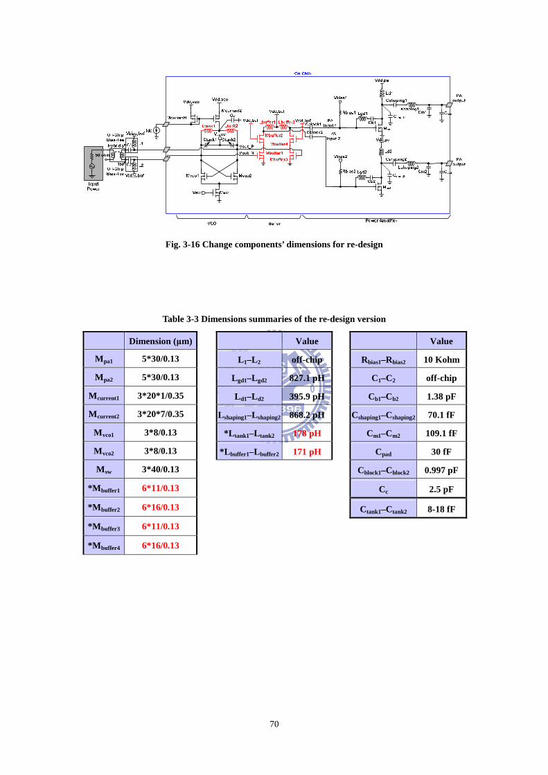
70
Fig. 3-16 Change components’ dimensions for re-design
Table 3-3 Dimensions summaries of the re-design version
Dimension (µm)
M pa1 5*30/0.13
M pa2 5*30/0.13
M current1 3*20*1/0.35
M current2 3*20*7/0.35
M vco1 3*8/0.13
M vco2 3*8/0.13
M sw 3*40/0.13
*M buffer1 6*11/0.13
*M buffer2 6*16/0.13
*M buffer3 6*11/0.13
*M buffer4 6*16/0.13
Value
L1–L2 off-chip
Lgd1–Lgd2 827.1 pH
L d1–Ld2 395.9 pH
L shaping1–Lshaping2 868.2 pH
*L tank1–Ltank2 178 pH
*L buffer1–Lbuffer2 171 pH
Value
Rbias1–Rbias2 10 Kohm
C1–C2 off-chip
Cb1–Cb2 1.38 pF
Cshaping1–Cshaping2 70.1 fF
Cm1–Cm2 109.1 fF
Cpad 30 fF
Cblock1–Cblock2 0.997 pF
Cc 2.5 pF
Ctank1–Ctank2 8-18 fF

71
Fig. 3-17 The modified layout for re-design whole circuits
0.0 0.1 0.2 0.3 0.4 0.5 0.6 0.7 0.8 0.9 1.0 1.1 1.222.6
22.8
23.0
23.2
23.4
23.6
23.8
24.0
24.2
24.4
24.6
24.8
25.0
Fre
qu
ency
(G
Hz)
Tuning Voltage (V)
Post-Sim(Original) Post-Sim(Revised) Post-Sim(Re-Design)
Fig. 3-18 Output frequency of re-design comparing with original and revised post-sim

72
0.0 0.1 0.2 0.3 0.4 0.5 0.6 0.7 0.8 0.9 1.0 1.1 1.2-8
-6
-4
-2
0
2
4
6
8
10
12
Ou
tpu
t P
ow
er (
dB
m)
Tuning Voltage (V)
Post-Sim(Original) Post-Sim(Revised) Post-Sim(Re-Design)
Fig. 3-19 Output power of re-design comparing with original and revised post-sim
1000 10000 100000 1000000 1E7 1E8-120
-100
-80
-60
-40
-20
0
Ph
ase
No
ise
(dB
c)
Frequency (Hz)
Post-Sim(Original) Post-Sim(Revised) Post-Sim(Re-Design)
Fig. 3-20 Phase noise of re-design comparing with original and revised post-sim

73
-30 -25 -20 -15 -10 -5 0 5 10 15-45
-40
-35
-30
-25
-20
-15
-10
-5
0
5
10
15
Ou
tpu
t P
ow
er (
dB
m)
Input Power (dBm)
Post-Sim(Original) Post-Sim(Revised) Post-Sim(Re-Design)
Fig. 3-21 Pout vs Pin of re-design comparing with original and revised post-sim
-30 -25 -20 -15 -10 -5 0 5 10 15-80
-70
-60
-50
-40
-30
-20
-10
0
10
20
30
40
PA
E &
Dra
in E
ffic
ien
cy (
%)
Input Power (dBm)
Drain Efficiency (Original Postsim) PAE (Original Postsim) Drain Efficiency (Revised Postsim) PAE (Revised Postsim) Drain Efficiency (Redesign Postsim) PAE (Redesign Postsim)
Fig. 3-22 PAE and drain efficiency vs Pin of re-design comparing with original and revised
post-sim

74
Table 3-4 Comparison with other K-band power amplifiers
Post-Sim (Re-Design) [9] [13]
Technology 0.13-µµµµm CMOS 0.13-µµµµm CMOS 0.18-µµµµm CMOS
Topology Class E Power Amplifier Class E Power
Amplifier
Class AB Power
Amplifier
Supply Voltage (V) 1.2 1.5 2.5
Power Consumption
(mW) 32.7 52.5 170
Frequency (GHz) 24.26 18 24
PAE (%) 27.82 23.5 6.5
Drain Efficiency (%) 32.91 23.43 14.78
Max. Pout (dBm) 10.41 10.9 14
Chip Area (mm2) 1.05 0.78 14.28
Table 3-5 Comparison with other K-band power amplifiers
Post-Sim (Re-Design) *[10] [11] [12]
Technology 0.13-µµµµm CMOS 0.13-µµµµm CMOS 0.18-µµµµm CMOS 0.18-µµµµm CMOS
Topology Class E Power Amplifier Class AB Power
Amplifier
Class A Power
Amplifier
Class A Power
Amplifier
Supply Voltage (V) 1.2 1.2 3.6 3.6
Power Consumption
(mW) 32.7 349.9 885.6 504
Frequency (GHz) 24.26 24 18-23 24
PAE (%) 27.82 23.9 9.3 20
Drain Efficiency (%) 32.91 29.3 11.55 31.45
Max. Pout (dBm) 10.41 17.1 20.1 22
Chip Area (mm2) 1.05 1.05 0.79 0.42
*[10] : redesign post-sim results of proposed power amplifier in [10]

75
Table 3-6 Summaries of re-design post-sim results
Post-Sim
(Original) Measurement
Post-Sim
(Revised)
Post-Sim
(Re-Design) Spec.
RF (GHz) 24.4 23.2 23.5 24.26 24
Voltage-Controlled
Oscillator with
Cascode Buffer
15.3 13.7 15.2 23.4 -
Power Amplifier 31.1 15.7 10.9 32.7 -
Pow
er (
mW
)
Total 46.4 29.4 26.1 56.1 -
Tuning Range (GHz) 0.795 0.602 0.632 0.492 -
Phase Noise @ 10
MHz (dBc) -117 -108 -120 -119.9 -
Max. Pout (dBm) 10.15 -2.41 2.47 10.41 >10
Who
le C
ircui
ts
Overall Drain
Efficiency (%) 22.31 1.95 6.77 19.59 -
Cas
code
Buf
fer
with
Pow
er A
mpl
ifier
Peak PAE (%) 21.25 - - 19.83 -

76
Table 3-7 Ron case comparisons
Ron Case (Re-Design Postsim) w/o Ron Case (Re-Design Postsim)
Technology 0.13-µµµµm CMOS 0.13-µµµµm CMOS
Topology Class E Power Amplifier Class E Power Amplifier
Supply Voltage (V) 1.2 1.2
Power Consumption (mW) 32.7 21
Frequency (GHz) 24.26 24.26
PAE (%) 27.82 14.9
Drain Efficiency (%) 32.91 26.89
Max. Pout (dBm) 10.41 7.51

77
Chapter 4
Conclusions and Future Work
4.1. Conclusions
In this research, 1.2-V K-band front-end circuits consisted of voltage-controlled
oscillator and class E power amplifier are designed and measured. The power
amplifier is realized by one-stage differential push-pull amplifier, and the
voltage-controlled oscillator is realized by differential cross coupled LC tank
voltage-controlled oscillator. This is the first work including a voltage-controlled
oscillator and a power amplifier for K-band applications. A neutralization technique to
improve isolation also has been developed instead of the cascode architecture.
Because of the layout mistake and incorrect post simulation procedure, the
measured performance is seriously degraded. Measurement results show that the
measured output center frequency and maximum output power are 23.2 GHz
and –2.41 dBm, respectively. The measured phase noise is -108 dBc at 10 MHz. The
measured output power of cascode buffer with power amplifier is lower than original
post layout simulation about 13 dB. And the measured power consumption is 29.4
mW from 1.2 V power supply.
As after carefully considering these effects, the post layout simulation results of the
re-design circuits show that the output center frequency and maximum output power
are 24.26 GHz and 10.41 dBm, respectively. The phase noise is -119.9 dBc at 10 MHz.
The output power of cascode buffer with power amplifier is almost the same to the
original post layout simulation. And the total power consumption is 56.13 mW from
1.2 V power supply.
Even though the measured performance is seriously degraded, the advantages of

78
class E power amplifier approach can be noticed by post-sim results of the original or
re-design circuits. Comparing to other works, this power amplifier has higher drain
efficiency and PAE under lower supply voltage. Therefore, class E power amplifiers
are suitable for high efficiency application, especially for advanced CMOS
technology.

79
4.2. Future Work
Because the problem of frequency drift is occurred in measurement results, the
re-design version is moved to 24.26 GHz by careful whole chip EM simulation. This
re-design circuit will be tape-out and measured in the future. On-chip transformers at
differential input and output will be integrated in next version. Polar loop structure
will be designed in order to improve the linearity required of power amplifier in the
future.

80
References [1] ETSI EN 302 288-1 V1.1.1.
[2] Federal Communications Commission (FCC) 02-04, Section 15.249.
[3] Federal Communications Commission (FCC) 02-04, Section 15.515.
[4] Federal Communications Commission (FCC)
website .(http://wireless.fcc.gov/auctions/default.htm?job=release&id=3578&y
=2007), Auctions Datas, Band Plans, 24 GHz.
[5] E. Afshari, H. Bhat, X. Li, and A. Hajimiri, “Electrical funnel: a broadband
signal combining method,” in IEEE Int. Solid-State Circuits Conf. (ISSCC) Dig.
Tech. Papers, Feb. 2006, pp. 206–207.
[6] A. Komijani and A. Hajimiri, “A 24 GHz, +14.5 dBm fully integrated power
amplifier in 0.18 µm CMOS,” in Proc. IEEE Custom Integrated Circuits Conf.,
Oct. 2004, pp. 561–564.
[7] Abbas Komijani, and Ali Hajimiri, “A Wideband 77-GHz, 17.5-dBm Fully
Integrated Power Amplifier in Silicon,” in IEEE Journal of Solid-State Circuits
(JSSC), VOL. 41, NO. 8, AUGUST 2006, pp. 1749-1756.
[8] J.-L. Kuo, Z.-M. Tsai, and H. Wang, “A 19.1-dBm fully-integrated 24 GHz
power amplifier using 0.18-µm CMOS technology,” in Proc. EuMA, Oct. 2008,
pp. 1425–1428.
[9] C. Cao, H.-F. Xu, Y. Su, and K. K. O, “An 18-GHz, 10.9-dBm fully-integrated
power amplifier with 23.5% PAE in 130-nm CMOS,” in Proc. ESSCIRC, Sep.
2005, pp. 137–140.
[10] C.-Y. Wu, S.-W. Hsu, and W.-C Wang, “A 24-GHz CMOS current-mode
power amplifier with high PAE and output power,” in Proc. IEEE ISCAS, 2007,
pp. 2866–2869.
[11] C.-C. Hung, J.-L. Kuo, K.-Y. Lin, and H. Wang, “A 22.5-dB gain, 20.1-dBm
output power K-band power amplifier in 0.18-µm CMOS,” in Proc. IEEE
RFICS, 2010, pp. 557–560.
[12] P.-C. Huang, J.-L. Kuo, Z.-M. Tsai, K.-Y. Lin and H. Wang, “A 22-dBm
24-GHz power amplifier using 0.18-µm CMOS technology,” in Proc. IEEE
IMS, 2010, pp. 248–251. [13] A. Komijani, A. Natarajan, and A. Hajimiri, “A 24-GHz, +14.5-dBm fully
integrated power amplifier in 0.18-µm CMOS,” IEEE J. Solid-State Circuits,
vol. 40, no. 9, pp. 1901–1908, Sep. 2005.
[14] N.O. Sokal and A.D. Sokal. Class E-a new class of high efficiency tuned
single-ended switching power amplifier. Journal of Solid-State Circuits,
vol.sc-10, no. 3, Jun. 1975.

81
[15] Patrick Reynaert, Koen L. R. Mertens, and Michiel S. J. Steyaert, “A
state-space behavioral model for CMOS class E power amplifiers,” IEEE
Transactions on Computer-Aided Design of Integrated Circuits and Systems,
vol. 22, no. 2, Feb. 2003
[16] Guillermo Gonzalez, “MICROWAVE TRANSISTOR AMPLIFIERS Analysis
and Design,” SECOND EDITION.


![1.yËë ï¬æ Â ï¬ ¦æ´Æ礯ÞÚ » U b{ 1.yÏá¿Ñ£Ã Æ Âz …... Òçp Ëë ï¬æ  ﬡ ]qÑ迳áÚ¢ çÅÍ Æ¿ÓçÎx Ñ Ûæ µ» çp Ëë ïÛá ´¿«qÑå¼ïµ](https://static.fdocuments.net/doc/165x107/5e38321613ad7e45a55dc036/1y-u-b-1yf-z-.jpg)

