NXP PCD6001, PCD6002 Data Sheet - Keil · •Embedded DTMF detection, call progress detection,...
96
DATA SHEET Product specification Supersedes data of 2001 Feb 05 File under Integrated Circuits, IC17 2001 Apr 17 INTEGRATED CIRCUITS PCD6001 Digital telephone answering machine chip
-
Upload
trankhuong -
Category
Documents
-
view
237 -
download
2
Transcript of NXP PCD6001, PCD6002 Data Sheet - Keil · •Embedded DTMF detection, call progress detection,...

DATA SHEET
Product specificationSupersedes data of 2001 Feb 05File under Integrated Circuits, IC17
2001 Apr 17
INTEGRATED CIRCUITS
PCD6001Digital telephone answeringmachine chip

2001 Apr 17 2
Philips Semiconductors Product specification
Digital telephone answering machine chip PCD6001
CONTENTS
1 FEATURES
2 APPLICATION SUMMARY
2.1 Metalink emulation
3 GENERAL DESCRIPTION
4 ORDERING INFORMATION
5 BLOCK DIAGRAM
6 PINNING INFORMATION
6.1 Pinning6.2 Pin description6.3 Pin types
7 FUNCTIONAL DESCRIPTION
7.1 Architecture7.2 I/O summary7.3 Overview of functional description
8 POWER SUPPLY, RESET AND START-UP
8.1 Power supply8.2 Reset and start-up
9 TICB - GENERATION AND SELECTION OFSYSTEM CLOCKS
9.1 Microprocessor, DSP, CODEC and IOM clockgeneration
9.2 System clocks9.3 Real-Time Clock generation
10 THE MICROCONTROLLER
10.1 Microcontroller architecture10.2 Memory mapping10.3 SFR mapping10.4 Microcontroller interrupts10.5 Interface to DSP10.6 Interface to Real-Time Clock (RTC)10.7 Interface to the Memory Control Block (MCB)10.8 The test registers CDTRx, PMTRx and TCTRL10.9 Interface to Timing and Control Block (TICB)10.10 Power and Interrupt Control Register (PCON)10.11 I2C-bus10.12 MSK modem10.13 LE control
11 DSP I/O REGISTERS
11.1 Interface to CODEC
12 EXTERNAL MEMORY INTERFACE
12.1 Supported flash memories12.2 DTAM external interface during target
debugging
13 THE CODECs
13.1 Definitions13.2 CODEC architecture
14 ANALOG VOLTAGE REFERENCE (AVR)
14.1 Bandgap reference14.2 Analog Voltage Source (AVS)
15 IOM
15.1 Features15.2 Pin description15.3 Functional description15.4 IOM data buffers15.5 IOM Control Register (IOMC)15.6 Timing
16 EXTERNAL I/O INTERFACES
16.1 External analog interfaces16.2 External digital Interfaces
17 ELECTRICAL CHARACTERISTICS
17.1 Limiting values17.2 Supply characteristics17.3 Digital I/O17.4 Analog supplies and general purpose ADC and
DAC17.5 CODECs
18 APPLICATION DIAGRAMS
19 PACKAGE OUTLINE
20 SOLDERING
20.1 Introduction to soldering surface mountpackages
20.2 Reflow soldering20.3 Wave soldering20.4 Manual soldering20.5 Suitability of surface mount IC packages for
wave and reflow soldering methods
21 DATA SHEET STATUS
22 DEFINITIONS
23 DISCLAIMERS
24 PURCHASE OF PHILIPS I2C COMPONENTS

2001 Apr 17 3
Philips Semiconductors Product specification
Digital telephone answering machine chip PCD6001
1 FEATURES
· Excellent speech quality at average:2.6, 3.2 or 5.2 kbits/s compression rate
· Excellent background noise suppression for speechquality improvement
· Speech compression rate selection: 2.6, 3.2 or5.2 kbits/s
· Speech decompression rate selection: 2.6, 3.2 or5.2 kbits/s
· Variable playback speed: 50%, 100% and 200% of realtime
· Voice prompt playback
· Philips International Language Library (PILL) supporttools available; coding at 2.6, 3.2 or 5.2 kbits/s
· Voice operated start message recording (VOX)
· Call progress detection by busy tone detection andprogrammable silence detection
· Recording time of minimum 20 minutes in 4-Mbit flashmemory (at 3.2 kbits/s)
· Excellent true full-duplex handsfree performanceprovided by Philips ‘phlux’ algorithm
· On-hook caller ID detection according to Bell 202 andV.23 standards, as well as DTMF caller ID support
· Caller Alerting Signal (CAS) - caller ID level 2
· Dual tone generation for DTMF, melody tones andinformation tones
· Optional dial tone detection, and optional ringingdetection using hardware Caller Identification (CID)interface
· DTMF detection (for remote control function) with localecho canceller for high reliability
· Digital volume control
· Mixed digital/analog adaptive limit and/or level control ofaudio input signals
· Programmable analog CODEC gain for easy interfacing
· Internal 80C51 microcontroller can operate as systemcontroller; with selectable operating frequenciesbetween 1 and 21 MHz
· Internal 80C51 microcontroller emergency operationdown to 2.2 V eliminates the need for external diallers intelephone answering machine applications
· Standard 80C51 development tools allow fast design ofMan-Machine-Interface (MMI) features
· On-board Minimum Shift Keying (MSK) modem forCT0/CT1 applications
· Two integrated differential bit stream Analog-to-DigitalConverters (ADCs) for high quality audio input
· Two integrated differential bitstream Digital-to-AnalogConverters (DACs) for high quality audio output
· Software selectable auxiliary CODEC input channel
· Up to 38 general purpose digital I/O lines (most of thembidirectional) including I2C-bus, available for connectionto keyboard, display, line interface, etc.
· On-chip 2-channel time multiplexed 8-bit generalpurpose ADC for e.g. parallel set detection and batteryvoltage measurement
· On-chip 8-bit general purpose DAC for e.g. speakeramplifier volume control
· Day and time stamp possibility using built-in Real-TimeClock
· Flexible speech memory interface for connection ofseveral types of speech flash memory (serial, CAD orparallel) and DRAM
· I2C master/slave bus for peripheral control or I2C-busspeech memory access
· Extensive power management support for battery andemergency operation, also allowing portable (voicememo) applications
· Digital IOM A/u-law interface for Slave or Master modeoperation at various bit rates
· Emergency operation from telephone line power only;microprocessor and DTMF generator continue tooperate in this mode
· On-chip software switchable supply voltage for electretmicrophone
· Single low supply voltage (2.2 to 2.8 V)
· Built-in single low-frequency, low-power, crystal orceramic resonator oscillator and on-chip PLL to reduceEMI
· Stand-alone operation with low cost PAL, NTSC andDTMF crystals
· API providing flash memory management functionssuch as speech, telephone or CID data storage
· Pin and software compatible with the PCD6002OTP-device (see Application note for restrictions).

2001 Apr 17 4
Philips Semiconductors Product specification
Digital telephone answering machine chip PCD6001
2 APPLICATION SUMMARY
The PCD6001 can be used in various applications, someof which are listed below. Refer to Chapter 18 for thecorresponding outline application diagrams.
· Stand-alone digital answering machine; with handsfree
· Feature phone with integrated digital answeringmachine and full-duplex handsfree
· Dual-line digital answering machines
· Analog cordless applications such as CT0/1 basestations; with handsfree and MSK modem function forRF digital data transmission
· Portable voice memo recorders
· Automotive applications - car status announcements forexample
· Low-cost desktop video conferencing
· IOM master/slave interface to connect directly to digitalsystems like ISDN and DECT.
2.1 Metalink emulation
Metalink emulation is supported with the standardpackage.
3 GENERAL DESCRIPTION
The PCD6001 integrates all the digital and analog speechmanagement and processing functions required for afeature-phone with integrated digital answering machine,or a stand-alone digital answering machine into a singlelow-cost chip.
Key hardware features which give the chip distinctadvantages in performance and application overcompetitive solutions include:
· The flexibility to change the MMI
· An easy-to-program standard 80C51 microcontrollerwith 32-kbyte internal ROM memory
· High 80C51 microprocessor power for system controllerfunctions of CT0/CT1 system control functions
· Up to 38 general purpose I/O lines for peripheral control
· I2C-bus interface
· Flexible flash memory control to interface to severaltypes of serial and parallel flash memory
· Two integrated 16-bit bitstream audio CODECs for truefull-duplex handsfree operation or dual-line stand-aloneanswering machine operation
· Internal Digital Speech Processor (DSP) for excellent‘HARMONY’ sinusoidal speech compression,decompression and variable playback speed
· Embedded DTMF detection, call progress detection,voice operated recording (VOX)
· High quality caller ID FSK demodulation and CallerAlerting Signal (CAS) detection for CID level 2
· Two channel telephone line input for caller ID FSK andaudio interfacing.
Philips provides a sophisticated API running on theinternal 80C51, allowing product developers to designtheir MMIs quickly to suit particular applications. The APItakes care of all flash memory and DSP managementtasks and can be enhanced on request.
For the pre-recorded voice prompts, the PhilipsInternational Language Library (PILL) tools are availablefor a standard multimedia PC platform under Windows 95.These tools provide a way to compile a range ofmulti-lingual voice prompts for efficient storage in thespeech (flash) memory. The PILL tools support variouslanguages and their grammar adaptations.
4 ORDERING INFORMATION
TYPENUMBER
PACKAGE TEMPERATURERANGE (°C)NAME DESCRIPTION VERSION
PCD6001H QFP80 plastic quad flat package; 80 leads (lead length 1.95 mm);body 14 ´ 20 ´ 2.8 mm
SOT318-2 - 25 to +70
PCD6001U U/10 sawn wafer on Film Frame Carrier (delivery as KnownGood Dies)
- - 25 to +70

2001 Apr 17 5
Philips Semiconductors Product specification
Digital telephone answering machine chip PCD6001
5 BLOCK DIAGRAM
handbook, full pagewidth
MGT427
32 KBYTEROMAND
EXTERNALINTERFACE
P4
I2C-BUS
MCB
P2
P0
MICROCONTROLLER80C51
PSEN
ALE, RDN, WRN
P4.3
3
2
11 to 4
80 to 73
72 to 65
62
1
64
63
ALE
EA
MA7 to MA0
P2.7 to P2.0
P0.7 to P0.0
P4.3
PSEN
WR
RD
55RSTIN
54TST
MSKIOMMICM
WATCHDOG
CODEC 2(ANALOG)
CODEC 2(DIGITAL)
MAIN andAUX RAM
56P4.0/LE
57P4.1/FSK
58P4.2/FSO
59P4.4/FSI
60P4.5/GPC
P1
14 to 18 P1.0/EX2 toP1.4/EX6
19P1.5
20P1.6/SCL
21P1.7/SDA
52
P3.7/MIN/DI
MA
P3
51
P3.6/MOUT2/
FSC
50
P3.5/T1
49
P3.4/T0
48
P3.3/EX1N
47
P3.2/EX0N
46
P3.1/MOUT1/
DCK
45
26
SPKRM24
MICP25
VMIC
ANALOGVOLTAGE
REFERENCEand SUPPLY
27
VBGP29
VREF30
DAOUT
GENERALPURPOSE
A/D and D/A33
AD1IN32
AD0IN31
SPKRP23
LIFMIN2
CODEC 1(ANALOG)
CODEC 1(DIGITAL)
36
LIFPIN35
LIFMIN137
LIFPOUT39
LIFMOUT38
P3.0/MOUT0/
DO
XTAL1
OSCILLATORand PLL
TICB
PCD6001
idle
events m C_CLKDMI
RSTANA
CLK
main bus
wake-up
DSPCLK
DSPplus
ROM,RAM
42
XTAL241
VSSA
VSSPLL
WAKE-UP28
VDDA
VDDPLL
34
43 40 53 12 44
VSS3V1VDD3V1 VSS3V2VDD3V2
13 61 22
VSS3V3VDD3V3
Fig.1 Block diagram.

2001 Apr 17 6
Philips Semiconductors Product specification
Digital telephone answering machine chip PCD6001
6 PINNING INFORMATION
6.1 Pinning
handbook, full pagewidth
PCD6001
MGT428
1
2
3
4
5
6
7
8
9
10
11
12
13
14
15
16
17
18
19
20
60
59
58
57
56
64
63
62
61
55
54
53
52
51
50
49
48
47
46
45
44
43
42
41
P4.5/GPC
P4.4/FSI
P4.2/FSO
P4.1/FSK
P4.0/LE
WR
RD
P4.3
VSS3V2
RSTIN
TST
VDD3V1
P3.7/MIN/DI
P3.6/MOUT2/FSC
P3.5/T1
P3.4/T0
P3.3/EX1N
P3.2/EX0N
P3.1/MOUT1/DCK
P3.0/MOUT0/DO
VDD3V3
VDDPLL
XTAL1
XTAL2
MA1
MA2
MA3
MA4
MA5
PSEN
EA
ALE
MA0
MA6
MA7
VDD3V2
VSS3V1
P1.0/EX2
P1.1/EX3
P1.2/EX4
P1.3/EX5
P1.4/EX6
P1.5
P1.6/SCL
P1.7/SDA
VSS3V3
SPKRP
SPKRM
21
22
23
24
25 26 27 28 29 30 31 32 33 34 35 36 37 38 39 40
MIC
P
MIC
M
VM
IC
VS
SA
VB
GP
VR
EF
AD
0IN
AD
1IN
DA
OU
T
VD
DA
LIF
PIN
LIF
MIN
2
LIF
MIN
1
LIF
MO
UT
LIF
PO
UT
VS
SP
LL
P2.
7
P2.
6
P2.
5
P2.
4
P2.
3
P2.
2
P2.
1
P2.
0
P0.
7
P0.
6
P0.
5
P0.
4
P0.
3
P0.
2
P0.
1
P0.
0
80 79 78 77 76 75 74 73 72 71 70 69 68 67 66 65
Fig.2 Pin configuration.

2001 Apr 17 7
Philips Semiconductors Product specification
Digital telephone answering machine chip PCD6001
6.2 Pin description
Table 1 QFP80 package
SYMBOL PIN I/ORESETSTATE
PIN TYPE(1) DESCRIPTION
PSEN 1 O H ucp4mthuwh program store enable (80C51)
EA 2 I Z ucp4mthuwh external access NOT (80C51)
ALE 3 O H ucp4mthuwh address latch enable signal (80C51)
MA0 4 O L ops10c general purpose output; EA = 1; add_low; EA = 0
MA1 5 O L ops10c general purpose output; EA = 1; add_low; EA = 0
MA2 6 O L ops10c general purpose output; EA = 1; add_low; EA = 0
MA3 7 O L ops10c general purpose output; EA = 1; add_low; EA = 0
MA4 8 O L ops10c general purpose output; EA = 1; add_low; EA = 0
MA5 9 O L ops10c general purpose output; EA = 1; add_low; EA = 0
MA6 10 O L ops10c general purpose output; EA = 1; add_low; EA = 0
MA7 11 O L ops10c general purpose output; EA = 1; add_low; EA = 0
VDD3V2 12 power supply positive supply 2 (3.0 V) for digital circuitry
VSS3V1 13 power supply ground supply 1 for digital circuitry
P1.0/EX2 14 I/O H ucp4mthuwh 80C51 port pin/EX2 input
P1.1/EX3 15 I/O H ucp4mthuwh 80C51 port pin/EX3 input
P1.2/EX4 16 I/O H ucp4mthuwh 80C51 port pin/EX4 input
P1.3/EX5 17 I/O H ucp4mthuwh 80C51 port pin/EX5 input
P1.4/EX6 18 I/O H ucp4mthuwh 80C51 port pin/EX6 input
P1.5 19 I/O H ucp4mthuwh 80C51 port pin
P1.6/SCL 20 I/O Z I2C400k 80C51 port pin/I2C-bus clock
P1.7/SDA 21 I/O Z I2C400k 80C51 port pin/I2C-bus data
VSS3V3 22 power supply ground supply 3 for digital circuitry
SPKRP 23 O Z ana positive output to speaker from CODEC2 (handsfree)
SPKRM 24 O Z ana negative output to speaker from CODEC2 (handsfree)
MICP 25 I 0.625 V ana positive input from microphone to CODEC2 (handsfree)
MICM 26 I 0.625 V ana negative input from microphone to CODEC2 (handsfree)
VMIC 27 O Z ana positive microphone supply voltage (2 V)
VSSA 28 power supply ground supply voltage for analog circuits
VBGP 29 O 1.25 V band gap output voltage (VBGP)
VREF 30 O 2.00 V ana reference voltage (VREF)
AD0IN 31 I - ana analog input channel 1 for general purpose ADC
AD1IN 32 I - ana analog input channel 2 for general purpose ADC
DAOUT 33 O 0.5VDDA ana analog output channel for general purpose D/A converter
VDDA 34 power supply positive supply (2.5 V) for analog circuits
LIFPIN 35 I 0.625 V ana positive analog input of CODEC1 (line CODEC)
LIFMIN2 36 I 0.625 V ana negative analog input 2 of CODEC1 (line CODEC)
LIFMIN1 37 I 0.625 V ana negative analog input 1 of CODEC1 (line CODEC)
LIFMOUT 38 O Z ana negative analog output of CODEC1 (line CODEC)

2001 Apr 17 8
Philips Semiconductors Product specification
Digital telephone answering machine chip PCD6001
LIFPOUT 39 O Z ana positive analog output of CODEC1 (line CODEC)
VSSPLL 40 power supply ground supply for XTAL clock and PLL circuitry
XTAL2 41 O running ana crystal oscillator output
XTAL1 42 I - ana crystal oscillator input
VDDPLL 43 power supply positive supply (2.5 V) for XTAL clock and PLL circuitry
VDD3V3 44 power supply positive supply 3 (3.0 V) for digital circuitry
P3.0/MOUT0/DO 45 I/O H ucp4mthuwh 80C51 port pin/MSK output 0/IOM data output
P3.1/MOUT/DCK 46 I/O H ucp4mthuwh 80C51 port pin/MSK output 1/IOM DCK signal
P3.2/EX0N 47 I/O H ucp4mthuwh 80C51 port pin/EX0N input
P3.3/EX1N 48 I/O H ucp4mthuwh 80C51 port pin/EX1N input
P3.4/T0 49 I/O H ucp4mthuwh 80C51 port pin/Timer 0 input
P3.5/T1 50 I/O H ucp4mthuwh 80C51 port pin/Timer 1 input
P3.6/MOUT2/FSC 51 I/O H ucp4mthuwh 80C51 port pin/MSK output 2/IOM FSC signal
P3.7/MIN/DI 52 I/O H ucp4mthuwh 80C51 port pin/MSK input/IOM data input
VDD3V1 53 power supply positive supply 1 (2.5 V) for digital circuitry
TST 54 I - iptd test input (recommended to be connected to ground)
RSTIN 55 I - ipth reset in
P4.0/LE 56 I/O L ucp4mthuwh general purpose I/O/LCD enable, configured as OD afterreset
P4.1/FSK 57 I/O Z ucp4mthuwh general purpose I/O/Flash Serial Clock, configuredas OD after reset
P4.2/FSO 58 I/O Z ucp4mthuwh general purpose I/O/Flash Serial Out, configured as ODafter reset
P4.4/FSI 59 I/O Z ucp4mthuwh general purpose I/O/Flash Serial In, configured as ODafter reset
P4.5/GPC 60 I/O L ucp4mthuwh general purpose I/O/GP clock output (crystal clock ormicrocontroller clock), configured as OD after reset
VSS3V2 61 power supply negative supply 2 (ground) for digital circuitry
P4.3 62 I/O Z ucp4mthuwh general purpose I/O, configured as OD after reset
RD 63 O Z ucp4mthuwh 80C51 read NOT, configured as OD after reset
WR 64 O Z ucp4mthuwh 80C51 write NOT, configured as OD after reset
P0.0 65 I/O Z uceda4mtuwh 80C51 Port 0 input/output
P0.1 66 I/O Z uceda4mtuwh 80C51 Port 0 input/output
P0.2 67 I/O Z uceda4mtuwh 80C51 Port 0 input/output
P0.3 68 I/O Z uceda4mtuwh 80C51 Port 0 input/output
P0.4 69 I/O Z uceda4mtuwh 80C51 Port 0 input/output
P0.5 70 I/O Z uceda4mtuwh 80C51 Port 0 input/output
P0.6 71 I/O Z uceda4mtuwh 80C51 Port 0 input/output
P0.7 72 I/O Z uceda4mtuwh 80C51 Port 0 input/output
P2.0 73 O L ucp4mthuwh general purpose output, EA = 1; add_high; EA = 0
P2.1 74 O L ucp4mthuwh general purpose output, EA = 1; add_high; EA = 0
SYMBOL PIN I/ORESETSTATE
PIN TYPE(1) DESCRIPTION

2001 Apr 17 9
Philips Semiconductors Product specification
Digital telephone answering machine chip PCD6001
Note
1. The pin type codes are explained in Section 6.3.
P2.2 75 O L ucp4mthuwh general purpose output, EA = 1; add_high; EA = 0
P2.3 76 O L ucp4mthuwh general purpose output, EA = 1; add_high; EA = 0
P2.4 77 O L ucp4mthuwh general purpose output, EA = 1; add_high; EA = 0
P2.5 78 O L ucp4mthuwh general purpose output, EA = 1; add_high; EA = 0
P2.6 79 O L ucp4mthuwh general purpose output, EA = 1; add_high; EA = 0
P2.7 80 O L ucp4mthuwh general purpose output, EA = 1; add_high; EA = 0
SYMBOL PIN I/ORESETSTATE
PIN TYPE(1) DESCRIPTION
6.3 Pin types
6.3.1 POWER SUPPLY PINS
There are 6 different power supply domains (see Fig.3):
· Digital core circuit (2.5 V): VDD3V1/VSS3V1
· Digital periphery circuit (3.0 V): VDD3V2/VSS3V2 andVDD3V3/VSS3V3
· PLL circuits and crystal oscillator (2.5 V): VDDPLL andVSSPLL
· Analog circuits (2.5 V): VDDA and VSSA.
All VSS pins must be connected to the same ground planeon the Printed-Circuit Board (PCB). All 2.5 V VDD pinsmust be connected to the same power supply. All VDD pinshave to be separately decoupled, according to Chapter 18.
6.3.2 ANALOG PINS
· ana: full ESD protected analog I/O pad (doubleprotection diode).
6.3.3 DIGITAL PINS
· ucp4mthuwh: 4 mA 80C51 I/O pins
· uceda4mtuwh: 4 mA 80C51 I/O pins with input enable
· iptd: input pad buffer; pull-down
· ipth: input pad buffer with Schmitt trigger
· ops10c: output pad; push-pull; 4 mA output drive; 10 nsslew control
· I2C400k: bidirectional open-drain I2C-bus compatiblepad.
handbook, halfpage
MGT429
VDD3V1
VSS3V1
VDD3V2
VSS3V2
VDD3V3
VSS3V3
VDDPLL
VSSPLL
VDDA
VSSA
Fig.3 PCD6001 chip supply rails with protection diodes.

2001 Apr 17 10
Philips Semiconductors Product specification
Digital telephone answering machine chip PCD6001
7 FUNCTIONAL DESCRIPTION
7.1 Architecture
The PCD6001 architecture is based on an embedded 8-bit80C51 microcontroller, a Philips ‘REAL’ DSP core, twohigh quality AD/DA CODECs and a 32-kbyte ROMmicrocontroller memory. Refer to the block diagram inChapter 5.
The most important DSP peripherals are the:
· CODECs
· DSP program ROM
· DSP RAM
· IOM interface.
The most important microcontroller peripherals are the:
· Memory Control Block (MCB)
· Watchdog Timer
· General purpose ports
· I2C-bus interface
· MSK block (used for digital data transfer and analoguecordless applications).
The MCB, through Ports P0, P2, P4 and MemoryAddress (MA) can interface to various types of flashmemory including serial, parallel or multiplexedcommand/address/data. Most of the peripherals arecontrolled via microcontroller special function registers.
The microcontroller initializes and controls the:
· DSP via the DSP to Microcontroller Interface (DMI)
· Speech flash memory via the Memory ControlBlock (MCB), and P0/P4 port pins
· Clock and power settings via the Timing and ControlBlock (TICB)
· Analog section via its Special Function Registers (SFR).
7.2 I/O summary
All digital I/O for peripherals such as keyboard, display,line interface and others are handled by themicrocontroller via ports P0, P1, P2, P3, P4, and MA.
Port 2 and MA provide 16 general purpose output-onlylines (not bit-addressable, push-pull, 4 mA) to driveperipherals. These ports can be used for peripheral controlif EA is logic 1. The 4 mA driving level should be adequateto drive a low power LED directly if required.
In addition to these 16 output-only lines, 16 generalpurpose I/O lines are provided by Ports 1 and 3. Port 1can handle 5 external interrupts (P1.0 to P1.4) that arealso HIGH/LOW interrupt level programmable. Port 1 alsocontains the I2C-bus. Port 3 can handle an additional2 external interrupts (P3.2 and P3.3) which are activeLOW only. The Timer 0 and Timer 1 inputs are availableon Port 3 as for the standard 80C51. Ports 1 and 3 are80C51 weak pull-up I/O lines with a 4 mA sink capability,with the exception of the I2C-bus lines P1.6 and P1.7which are open-drain. If the P3 alternate port function forthe MSK modem is chosen then the standard I/O is notavailable on pins P3.0, P3.1, P3.6 and P3.7.
Port 4 lines are 6 more general purpose I/O. They will beconfigured as open-drain after reset. These open-drainscan be connected via pull-up resistors to the telephonesystem supply or to the mains AC supply. If a flashmemory with a different supply voltage (VDD_FLASH upto 3.3 V) is connected, P4.3 can be pulled-up to thisvoltage. This is required such that the Chip EnableNot (CEN) input of a flash device is equal to VDD_FLASH toreduce the standby power consumption. All other Port 4pins should not be pulled up to a voltage higher thanVDD_DTAM.
In case a CAD flash is used, P4.4 and P4.5 are freebit-addressable ports.
All P4 pins also can be configured to push-pull via theregister P4CFG. This brings the total of I/O lines to 38 (ofwhich 16 are output only).
In case an I2C-bus LCD driver is used, P4.0, at whicha Latch Enable (LE) function is provided for 68xxx familymicrocontroller peripherals, is an additional freebit-addressable open-drain I/O port.
The analog interfacing for the PCD6001 consists of theanalog audio I/O of the 2 CODECs and 2 additionalgeneral purpose analog-to-digital inputs and a generalpurpose digital-to-analog output for voltage measurementand control respectively. Furthermore a stabilizedmicrophone supply output VMIC is provided which can beswitched on/off for power control.
One audio CODEC is dedicated for the PSTN linecommunication (CODEC1). This line CODEC has adifferential low ohmic analog output which consists ofLIFPOUT and LIFMOUT. In case only one of thedifferential outputs is used, LIFPOUT should be chosen,since the Emergency mode DTMF signal is also available.

2001 Apr 17 11
Philips Semiconductors Product specification
Digital telephone answering machine chip PCD6001
The line CODEC has 3 inputs which are configurable as2 single-ended inputs LIFMIN1 and LIFMIN2 that can beselected by software control, while LIFPIN is AC coupledto ground. It is also possible to use one of the LIFMINinputs (leaving the other unconnected) in conjunction withthe LIFPIN input as a differential input, in case a highCMRR is required.
The second CODEC is dedicated for a local microphoneand loudspeaker connection (CODEC2). This handsfreeCODEC has a differential low ohmic analog output whichconsists of SPKRP and SPKRM. This output can be usedeither differential or single ended. The speaker outputimpedance and driving level is not suitable to directlyconnect a speaker. The handsfree CODEC has adifferential microphone input which consists of MICP andMICM. This differential input features a fixed 16 dBmicrophone preamplifier.
Both the line and handsfree CODEC outputs have on-chipfiltering for out of band signals such that no external filtersare required.
There are 2 ´ 8-bit analog-to-digital inputs AD0IN andAD1IN for voltage measurements which can be used forparallel set detection algorithms or battery control. An 8-bitDAC output DAOUT can provide an analog peripheralcontrol signal.
7.3 Overview of functional description
The detailed functional description is divided into separatechapters covering the major functional blocks, as follows:
Chapter 8 “Power supply, reset and start-up”
Chapter 9 “TICB - generation and selection of systemclocks”
Chapter 10 “The microcontroller”
Chapter 11 “DSP I/O registers”
Chapter 12 “External memory interface”
Chapter 13 “The CODECs”
Chapter 16 “External I/O interfaces”.
8 POWER SUPPLY, RESET AND START-UP
8.1 Power supply
The PCD6001 core circuitry is supplied by three 3 V supplypairs. The crystal oscillator and PLL are supplied with aseparate pair of supply pins to provide a ‘clean’ supplyvoltage required for low jitter. The following supplies exist:
VDD3V1 and VSS3V1: digital core supply 1 (2.5 V)
VDD3V2 and VSS3V2: digital supply 2 (3.0 V)
VDD3V3 and VSS3V3: digital supply 3 (3.0 V)
VDDA and VSSA: analog supply (2.5 V)
VDDPLL and VSSPLL: crystal clock and PLL supply (2.5 V).
8.2 Reset and start-up
After applying the power supply voltage, the chip will needan external Power-on reset via pin RSTIN. RSTIN shouldremain active (logic 1) until Vtrh and has to become activeagain before the power supply drops below Vtrl.
The reset via RSTIN is one of 3 possible ways to performa reset. The following reset conditions exist:
· Wake-up from system off (crystal is off, but power is on)by an external interrupt
· RSTIN, reset in from pin RSTIN
· Watchdog Timer expires.
After a Power-on reset and after a wake-up from systemoff, a counter is activated, which guarantees that the firstinstruction fetch of the microcontroller is delayed by atleast 4096 clock cycles.
To reduce power consumption during reset, the followingreset strategy is used. If the DSP function is not required,it can be switched off by the microcontroller. The DSPreset will then be delayed (until it is switched on again), inorder to avoid a large (reset) power consumption.

2001 Apr 17 12
Philips Semiconductors Product specification
Digital telephone answering machine chip PCD6001
9 TICB - GENERATION AND SELECTION OFSYSTEM CLOCKS
The TICB generates the clocks for all digital chip blocks,and controls the on/off switching of these blocks by usingclock gating. The TICB is controlled via the microcontrollerSFR registers SYMOD, CKCON and SPCON. The TICBcontains:
· An input section to adapt to different input clock rates
· A clock generation section
· A clock selection section
· The Real-Time Clock for a 1 minute interrupt generation
· The microcontroller interrupt timers (FS_event andTIME_event) and the DSP interrupt timer (FS1) torespectively synchronize the microcontroller and DSPprocesses.
9.1 Microprocessor, DSP, CODEC and IOM clockgeneration
Figure 4 shows the TICB input section and the clockgeneration section.
The clock generation section contains a PLL to generatethe clock rates which are higher then the input clock rate.With the input section, a wider variety of input clockfrequencies can be adapted to the input frequency valuesneeded by the PLL (3.456 or 3.580 MHz).
In order to save power the PLL can be switched off. Thisshould however only be done when the chip is in theEmergency mode. When switching on the PLL, it takes40 m s (173 emergency clock periods) until the clockfrequencies are derived from the PLL output.
Table 2 gives a description of the signals and their valuesfor a crystal frequency of 3.456 and 3.580 MHz.
The clock generation section also contains logic tosynchronize the CODEC timing signals and the DSP andmicrocontroller interrupt timers to an external FrameSync. (FSC). This synchronization is only activated whenusing the IOM in Slave mode. If the IOM is activated inMaster mode, the TICB generates the DCK andFSC signals from CLK28.
Some of the clock signals can be made available asgeneral purpose clock, for various peripherals needing aclock source such as an PCA1070 line interface. Thisgeneral purpose clock (GPC) signal is an alternativeoutput of P4.5 and can be turned on with ALTP bit 3. WithALTP bit 2, the source for GPC can be defined. The GPCsource is EMG_CLK (normally 3.58 MHz) when bit 2 islogic 0 and the GPC source is m C_CLK when bit 2 is set tologic 1. As a spike-free GPC is not guaranteed whenswitching between these clocks, it is recommended to firstset the clock source before switching on the GPC. TheALTP register is described in more detail in Section 16.2.

2001 Apr 17 13
Philips Semiconductors Product specification
Digital telephone answering machine chip PCD6001
handbook, full pagewidth
MGT430
÷2
÷2
÷6
÷24
÷3
÷4
÷192
DCKGENERATOR
CLK3GEN
control and synchronization CODEC timing signals
CLK_21 CLK_3
CDCCNTRL
EMG_CLK
PLL ´ 24
on
CLK_IN
SYMOD[5]PLL_ON
CLK_28
CLK_21CLK_14
0
1
CLK_7
CLK_1
CLK3_EMG FSC
DCK
CLK_3
FS1
÷2 CLK_42
÷2
÷4
SYMOD[5]PLL_ON
SYMOD[6 or 7]
PLL_IN
20.736 MHzfor a 3.456 MHzPLL input clock
CLK3_CORR
CLK3_OUT
CKCON[6 or 7]
Fig.4 TICB input section and clock generation.

2001 Apr 17 14
Philips Semiconductors Product specification
Digital telephone answering machine chip PCD6001
Table 2 Descriptions and frequency values for signals shown in Fig.4
Notes
1. These values are only valid if the RTC mode bit CKCON.6 has been set according to the PLL_IN frequency used(see also Table 6).
2. If the IOM Slave mode is activated, these clock signals are synchronized to the externally applied FSC.
3. Proper IOM functionality is only guaranteed at DSP clock frequencies of 28 and 42 MHz. If the IOM Slave mode isactivated, the externally applied DCK and FSC signals are used.
4. These master frequencies do not comply to IOM specification. For 3.58 MHz crystal operation, proper IOMfunctionality is therefore only guaranteed in Master mode.
SIGNAL FUNCTIONVALUE (MHz)
PLL_IN 3.456 PLL_IN 3.580
Microprocessor and DSP clock signals
EMG_CLK emergency clock 3.456 3.580
CLK_42 DSP selectable clock frequency 41.472 42.960
CLK_28 DSP selectable clock frequency 27.648 28.640
CLK_21 microcontroller selectable clock frequency 20.736 21.480
CLK_14 microcontroller selectable clock frequency 13.824 14.320
CLK_7 DSP and microcontroller selectable clock frequency 6.912 7.160
CLK_1 DSP and microcontroller selectable clock frequency 1.152 1.193
CODEC clock signals
CLK_21 input clock for phase corrected CLK3_OUT 20.736 21.480
CLK3_EMG EMG_CLK input to CLK_3 multiplexer 3.456 3.580
CLK3_CORR frequency corrected CODEC clock (24/25 ´ 3.58 MHz) - 3.437(1)(2)
CLK3_OUT phase corrected 3.456 MHz CODEC clock 3.456(1)(2) -CLK14_CODEC input clock for CODECs 13.824 14.320
IOM clock/timing signals
DCKmaster the IOM master clock signal DCK generated by the TICB 1.536(1)(3) 1.527(1)(3)(4)
FSCmaster the IOM master frame sync FSC generated by the TICB 8 kHz(1)(3) 7.955 kHz(1)(3)(4)

2001 Apr 17 15
Philips Semiconductors Product specification
Digital telephone answering machine chip PCD6001
9.2 System clocks
Figure 5 shows the multiplexers with their input and control signals for the DSP processor clock, the microcontrollerclock, the CODEC clock (CLK_3) and the chip input clock frequency. The functional position of the CODEC clockmultiplexer is shown in Fig.4.
handbook, full pagewidth
MGT431
R S
QFF
CLK_3_DRT2
CLK_3_DRT1CLK_3
CDCCNTRL_CLK
DSP_IDLE
DSP_WAKEUP
DSP_CLK
m C_CLK
DSP_CLK_IN
EMG_CLK
EMG_CLK
EMG_CLK
CLK_1
CLK_7
CLK_14
CLK_21
CLK_1
CLK_7
CLK_42
CLK_28
CLK3_CORR
CLK3_OUT
CKCON[2, 3 or 7]
CKCON[4, 5 or 7]
CKCON[6 or 7]
CKCON[0 or 1]
SPCON[0 or 1] SPCON[2 or 3]
SPCON[4]
÷ 4 ÷ 2 ÷ 2 ÷ 5FS1
FS_event TIME_event
3 2 1 0
Fig.5 Clock and event rate selection.

2001 Apr 17 16
Philips Semiconductors Product specification
Digital telephone answering machine chip PCD6001
9.2.1 SELECTION OF SYSTEM CLOCKS
Selection of system clocks involves:
· Selection of the crystal input clock in conjunction withPLL on/off selection (SYMOD register)
· Selection of clocks for the DSP, microcontroller andCODEC, together with microcontroller timing interruptrates (CKCON register)
· Activation, deactivation of individual clocks ordeactivation of the whole TICB in order to get anoptimum power consumption (SPCON register).
SYMOD, SPCON and CKCON are SFR registers in thedigital section which can be directly accessed by themicrocontroller. Sections 9.2.2 to 9.2.4 summarize thecontrol registers and settings used for system clockselection.
The activation of the DSP, and the digital part of bothCODECs is controlled via the SPCON SFR.
The clock rates of the DSP and microcontroller, and themicrocontroller timing interrupt rates are set via theCKCON SFR.
9.2.2 ANALOG SYSTEM MODE REGISTER (SYMOD)
Table 3 Analog System Mode Register (SFR address C5H); reset state 00H
9.2.3 SYSTEM POWER AND CLOCK CONFIGURATION REGISTER (SPCON)
Table 4 System Power and Clock Configuration Register (SFR address 99H); reset state 00H
9.2.4 CLOCK CONTROL REGISTER (CKCON)
Table 5 Clock Control Register (SFR address 9AH); reset state 00H
7 6 5 4 3 2 1 0
input clock 1 input clock 0 PLL off/on VMIC off/on CODEC2; analog CODEC1; analog
D/A(loudspeaker)off/on
A/D(microphone)off/on
D/A(to_line)off/on
A/D(from_line)off/on
7 6 5 4 3 2 1 0
system off spare spare DSP on CODEC2; digital CODEC1; digital
D/A(loudspeaker)off/on
A/D(microphone)off/on
D/A(to_line)off/on
A/D(from_line)off/on
7 6 5 4 3 2 1 0
EMG mode RTC mode DSP clock 1 DSP clock 0 micro clock 1 micro clock 0 FS_event 1 FS_event 0

2001 Apr 17 17
Philips Semiconductors Product specification
Digital telephone answering machine chip PCD6001
Table 6 shows the input clock selection in the analogsection of the chip. Note that for 3.456 and 3.58 MHzcrystal input clock, no clock division is done prior toinputting it to the PLL. After reset the input clock divisionrate is by default 1. This means that applications using aninput clock frequency other than 3.456 or 3.580 MHz, willhave to set the proper division rate, after system start-up.Otherwise proper functionality of the analog blocks is notguaranteed.
Table 7 shows the microcontroller clock frequencies. InEmergency mode (bit 7 of CKCON reset), the EMG_CLKis input directly to the microcontroller. The values ofCKCON bits 2 and 3 are then irrelevant. Note thatEmergency mode operation is only designed for start-upand POTS mode condition. Peripheral blocks (such as theCODECs and the IOM block) are not guaranteed to workwhen CKCON bit 7 is reset.
Table 6 Input clock selection
Note
1. The PCD6001 timing system is based on the 3.456 MHz (or multiples) input clock frequency. In order to be able touse the low cost 3.58 MHz crystal or ceramic resonator, a clock frequency correction is needed for some blocks(RTC, CODEC and IOM). IOM will only operate in Master mode.
Table 7 Microcontroller clock selection
Notes
1. 6 clocks/cycle.
2. If the PLL is switched off when not in Emergency mode, the selected clock would not be available. The micro wouldhang up. Before CKCON.7 is set to logic 1, SYMOD.5 must be set to logic 1 to activate the PLL.
CKCON.6(RTC MODE)
SYMOD.7(input clock 1)
SYMOD.6(input clock 0)
INPUT CLOCKDIVISION RATIO
CHIP INPUT CLOCKFREQUENCY (MHz)
0 0 0 1 3.456
1 0 0 1 3.580(1)
0 0 1 2 6.912
0 1 0 4 13.824
CKCON.7(EMG mode)
CKCON.3(micro clock 1)
CKCON.2(micro clock 0)
SYMOD.5PLL on/off
MICROCONTROLLERCLOCK FREQUENCY (1)
0 X X X EMG_CLK
1 X X 0 do not use(2)
1 0 0 1 CLK_1
1 0 1 1 CLK_7
1 1 0 1 CLK_14
1 1 1 1 CLK_21

2001 Apr 17 18
Philips Semiconductors Product specification
Digital telephone answering machine chip PCD6001
Table 8 shows the DSP clock frequency settings. Settingthe DSP frequency to the correct value according to theoperation mode of the DSP is done by the ApplicationProgramming Interface (API). Please refer to the APIspecification for more details.
Table 9 shows CLK_3 selection (CKCON.6/CKCON.7according to Fig.4). The selection depends on the type ofcrystal which is connected (determined by RTC modesetting according to Table 6). The setting of CKCON [6:7],thus determines the selection of the CLK_3 source (seeTable 2 and Fig.4). If CKCON.7 = 0 to denote Emergencymode - CLK_3 will be derived from the EMG_CLK, asshown in the following tables.
The TICB provides two periodic outputs to themicrocontroller: FS_event and TIME_event. FS_event isprogrammable to 4 different rates. Both outputs arederived from and therefore synchronized to FS1. Theoutputs are connected to an interrupt input of themicrocontroller and called ‘Time_event interrupt’ and‘FS_event interrupt’ respectively. The selection of theFS_event interrupt rate is done via the CKCON SFR, seeSection 9.2.4. Figure 8 shows the generation of theseinterrupts. Table 10 shows the selection of the FS_eventrate. The FS1 clock is provided by the CDCCNTRL blockshown in Fig.4.
Table 8 DSP clock selection
Table 9 CODEC clock selection
Note
1. A phase corrected CLK_3 clock is not available in Emergency mode (CKCON.7 = 0). For a CLK_3 phase correction(CKCON.6 = 1), CLK_21 must be available.
Table 10 FS_event rate selection
CKCON.7(EMG mode)
CKCON.5(DSP clock 1)
CKCON.4(DSP clock 0)
SYMOD.5(PLL on/off)
DSP CLOCKFREQUENCY
0 X X X EMG_CLK
1 X X 0 no clock active
1 0 0 1 CLK_1
1 0 1 1 CLK_7
1 1 0 1 CLK_42
1 1 1 1 CLK_28
CKCON.7(EMG mode)
CKCON.6(RTC mode)
CLK_3 SOURCE
0 X EMG_CLK(1)
1 1 CLK3_CORR
1 0 CLK3_OUT
CKCON.1(FS_event 1)
CKCON.0(FS_event 0)
FS_event INTERRUPT RATE
0 0 FS1/16 500 Hz 2 ms
0 1 FS1/8 1 kHz 1 ms
1 0 FS1/4 2 kHz 500 m s
1 1 FS1 8 kHz 125 m s

2001 Apr 17 19
Philips Semiconductors Product specification
Digital telephone answering machine chip PCD6001
9.3 Real-Time Clock generation
The Real-Time Clock (RTC) divider provides a 1 minutetiming signal which is available as an interrupt to themicrocontroller. The RTC_CLK input clock is alwaysactive, whether the PLL is active or not. Thus the completechip can be set into Power-down mode (but not System-offmode), where the microcontroller can be woken up by theRTC to maintain the values for date and time. TheRTC_CLK is directly derived from the EMG_CLK inputclock signal.
Figure 6 shows the RTC clock generation. To divide a3.456 or a 3.580 MHz clock into a 1 minute RTC signal a28 bit counter is required to count 60 ´ 3.456 ´ 106 clockperiods. To determine the number of most significant bitsof this counter required for an accurate RTC, the maximumallowed time deviation per month and the crystal accuracyneed to be taken into account. The LSB of the 28 counterhas an accuracy of 1/(60 ´ 3.456 ´ 106) = 0.005parts-per-million (ppm). Since a normal crystal accuracy isabout 10 ppm it is tolerable to have only the 17 MSB of thecounter available (10/0.005 = 2000, which implies that the11 LSB can be disregarded), as shown in Fig.6.
If one month is set to 30 ´ 24 ´ 60 ´ 60 = 2.6 ´ 106seconds, 10 ppm deviation equals 26 seconds per monthor about 5 minutes per year.
Since there are 2 possible RTC_CLK values, 3.580 and3.456 MHz, there are 2 comparators selectable for the
RTC; COMP_3.580 and COMP_3.456. The nominal valueof these comparators are (11 LSB are set to logic 0):
COMP_3.580: CCD2800H (RTCON = A5H)
COMP_3.456: C5C1000H (RTCON = 82H).
In Section 9.2 the conditions for the RTC_MODE signalare described.To allow connection of various crystals orceramic resonators, as well as to provide adjustment of theRTC clock according to the crystal tolerance, 8 of the 17most significant bits of the comparators are programmablevia the SFR register RTCON. The binary values of thecomparators are then as shown in Table 11.
Since the accuracy of Q11 is 10 ppm, with the adjustmentof the RTC via RTCON an accuracy of ±5 ppm can beachieved. For an RTC pulse every 1 minute the outer limitsof the crystal frequency inputs which can be connectedare:
COMP_3.580 (max): CCFF800H ® 3.582600 MHz
COMP_3.580 (min): CC80000H ® 3.573897 MHz.
COMP_3.456 (max): C5FF800H ® 3.460267 MHz
COMP_3.456 (min): C580000H ® 3.451563 MHz.
The default value of RTCON for an input frequency3.58 MHz is A5H and for an input frequency of 3.456 MHzis 82H.
Table 11 Comparator contents
Q27 Q18 Q11
COMP_3.580 1 1 0 0 1 1 0 0 1 x x x x x x x x
COMP_3.456 1 1 0 0 0 1 0 1 1 x x x x x x x x
bit 7 ¬ RTCON® bit 0
handbook, full pagewidth
MGM770
17
17
17Q11 to Q27
EMG_CLK
Q10
Q0
28 BITRIPPLE
COMP_3.456
COMP_3.580
0
1
RTC_MODE0: RTC_CLK = 3.456 MHz1: RTC_CLK = 3.580 MHz
synch_reset
RTC_event
Fig.6 Real-Time Clock (RTC) generation.

2001 Apr 17 20
Philips Semiconductors Product specification
Digital telephone answering machine chip PCD6001
10 THE MICROCONTROLLER
The embedded MS80C51 microcontroller controls theDigital Telephone Answering Machine (DTAM) chip bymeans of Special Function Registers (SFRs). SFRs aredefined for the blocks MCB, TICB, PCON, DSP, I2C-bus,ports P1, P3 and P4, MA, MSK and ANA (the analogblocks). All of these (except SFR PCON) are shown in theblock diagram in Fig.1. The architecture of themicrocontroller itself and the interface to these blocks aredescribed in this chapter.
10.1 Microcontroller architecture
The microcontroller architecture and its environment isshown in Fig.7.
The microcontroller has some application-specificperipherals such as the I2C-bus, Watchdog Timer (WD),P1, P3, P4, MCB, External Interface with MA port, SFRs ofthe DSP block, the TICB and the ANA block. Most of thesefunctions and SFRs are located in the Application SpecificFunction block (ASF), see Fig.7.
The 80C51 core contains the 80C51 standard functionssuch as Timer 0 and Timer 1, power-down/idle states anda 15 vector dual-level interrupt controller INT15L2.Furthermore, the microcontroller contains the Metalinkenhanced hooks protocol which enables Metalinkemulation via ALE, PSEN, EA, P0 and P2. The externalprogram memory access is done via the standard Ports P0and P2. Connection of external flash memory is done viathe P4, P0 and P2 I/O pads. The microcontroller ClockDriver (CD) has no clock divider, which means that themicrocontroller operates on 6 microcontroller_CLK clocksper machine cycle.
The 80C51 has a few basic modes of operation: Reset,Normal, Metalink, Test (various) Idle and Power-down.Entering the Metalink mode can be done via inputs ALEand EA during a reset.
The Idle mode can be entered by setting the IDL bit in thePCON register. Leaving the Idle mode can be done via amaster reset (RSTIN), any external interrupt, aDSP_event, TIME_event or RTC_event, Timer 0 andTimer 1, I2C-bus interrupt, MSK_event or FS_event; ifthese interrupts are enabled.
The Power-down mode can be entered by setting thePD bit in PCON. The power-down logic of themicrocontroller will turn all microcontroller clocks off.
The TIME_event, DSP_event, RTC_event andEX2 to EX6 are mixed with EX0 (see Fig.10) and thereforemake use of the standard wake-up circuitry of the 80C51.These interrupts should be active for more than 6 clocks(read, modify, write of IRQ1 takes 1 instruction) toguarantee the interrupt for the microcontroller.
Setting the PD bit of PCON after setting the system-off bitof SPCON, will trigger the analog section to turn off theoscillator and therefore the whole chip. In order to keepstatic supply currents minimal, it is advised to switch off thedigital-to-analog part of the CODECs before going in thissystem-off mode. Wake-up from system-off can be donevia a RSTIN or an external interrupt EX0 to EX6 (if the EX0interrupt is enabled) or EX1 (if the EX1 interrupt isenabled). A wake-up from system-off will always reset thePCD6001. The EX interrupt condition should last morethan 4096 + 64 + 4 clocks to be sure that the interrupt ishandled when entering the normal mode. If the interrupt isshorter the microcontroller will only enter the normal modeafter the reset is gone.
10.2 Memory mapping
The memory map of the 80C51 is shown in Fig.8.In addition to all the SFRs, the microcontroller has128 bytes of directly addressable (DATA) memory,128 bytes of indirectly addressable (IDATA) memory and512 bytes of AUX RAM, the on-chip ‘MOVX’ addressable(XDATA) memory. On-chip XDATA memory access canbe disabled by setting the ARD bit in PCON to logic 1. Theinternal 32-kbyte ROM of microcontroller program (CODE)memory can be accessed when EA is set to logic 1.
Via Ports P0, MA, P2 and P4 it is possible to access up to512 kbytes of external speech data memory stored in aparallel flash memory. A CAD flash memory can also bemapped in this area. A serial (SPI or Microwire compatible)flash memory can be connected to P4 which is controlledby the MCB. Up to 64 kbytes of program (CODE) memorycan be connected to the P0, P2 and PSEN pads. This canbe any external program memory (like the MON51 targetdebug ROM) if EA is logic 0.
When the EAM SFR bit (P4CFG.5) is logic 0 (default afterreset), the XRAM-mapped control registers can only beaccessed if P4.3 is logic 1. Otherwise, XRAM addressingis independent of the value of the P4.3 SFR bit.

2001 Apr 17 21
Philips Semiconductors Product specification
Digital telephone answering machine chip PCD6001
handbook, full pagewidth
MGT432
IRQ1/IX1
GROUP IF
MSK
TICB
ANAANALOG
FUNCTIONS
DSP
I/O PADSP1, P3RD,WR
FLASHI2C-BUS
FLASHCAD
FLASHPARALLEL
FLASHMICROWIRE/
SPI
EXTERNAL64-kbyteSRAM
I/O PADSP4
DSP
CDMSEL
PORT1
WDWDRST
PORT3
MODECONTROL
RAMIF
CPU
XMEMU
PORT4
I PADRST_IN
I PADRST_ANA
O PADMRST
O PADDIS_XTAL
I2C-BUSI2C-bus_int
ARD PCON.2to
PCON.7
MCB
I/O PADSP0, P2PSEN
EAALE
SFGROUP INT.
TIMER 0TIMER 1PCON.0
toPCON.1INT15L2
SRAMMAIN/AUX
RAM256/512BYTES
APPLICATIONSPECIFIC
FUNCTIONS
EX0 to EX6
DSP_req
MSK_INT
ROMIF
INTERNAL32 KBYTE
ROM
m CMS 80C51 CORE
m C_CLK
MRST
osc_off
pad_alepad_ea_n
TICBIF
SPCON[7]
DSP_event
TIME_event
RTC_event
FS_event
TICB
DRAMARAM
Fig.7 Microcontroller (MS 80C51) architecture and environment.

2001 Apr 17 22
Philips Semiconductors Product specification
Digital telephone answering machine chip PCD6001
handbook, full pagewidth
MGT433
External programmemory
External datamemory
Internal XDATAmemory
Internal ROM
AUX RAM
ConfRegMAP2
EA = 1
XDATA
IDATA
Main RAM SFR
DATA
128
255
48
32
0
BITADDRESSABLE
SPACE
REGISTERBANKS 0 TO 3
P4.3 = XARD = X
P4.3 = 0ARD = 1
XDATAARD = 0
P4.3 = XARD = 1
CODE
CODE
64K
32K
518
515
512
EA = 1
XDATA-mapped registersP4.3 = 1, EAM = 0, ARD = Xor ARD = 0, EAM = 1, EA = 1
Fig.8 Microcontroller memory map.

2001 Apr 17 23
Philips Semiconductors Product specification
Digital telephone answering machine chip PCD6001
10.3 SFR mapping
The SFR mapping for the microcontroller is shown in Table 12. All SFRs and their reset states are described in Table 13.
Table 12 SFR mapping
Notes
1. SFRs in this column are both bit and byte-addressable.
2. Complies to 80C51 family architecture specification.
3. These registers are read only (all other SFRs are read/write).
4. Reserved register, used for testing purposes. Writing of reserved or undocumented bits might lead to unexpectedbehaviour of the device (see Section 10.8).
SFRADDRESS
(HEX)
SPECIAL FUNCTION REGISTERS 8 BITS EACH
ADDRESSABLE (1) ONLY BYTE ADDRESSABLE
F8 to FF IP1(2) - - - - - - WDT(2)
F0 to F7 B(2) - - - - - - WDTKEY
E8 to EF IEN1(2) IX1 - - - - - -E0 to E7 ACC(2) - - - - - - -D8 to DF S1CON(2) S1STA(2)(3) S1DAT(2) S1ADR(2) - - - -D0 to D7 PSW(2) - - - - - - -C8 to CF MCON MBUF MSTAT - - - - -C0 to C7 IRQ1 INTC GPADR(3) GPADC GPDAR SYMOD - DTCON
B8 to BF IP0(2) XWUD VREFR CDVC1 CDVC2 CDTR1(4) - TCTRL(4)
B0 to B7 P3(2) - - - - PMTR1(4) PMTR2(4) CDTR2(4)
A8 to AF IEN0(2) MCSC MCSD ALTP - - - -A0 to A7 - - DTM0(3) DTM1(3) DTM2(3) MTD0 MTD1 MTD2
98 to 9F P4 SPCON CKCON RTCON - CDTR1(4) - P4CFG
90 to 97 P1(2) - - - - - - -88 to 8F TCON(2) TMOD(2) TL0(2) TL1(2) TH0(2) TH1(2) - -80 to 87 - SP(2) DPL(2) DPH(2) - - - PCON

2001 Apr 17 24
Philips Semiconductors Product specification
Digital telephone answering machine chip PCD6001
Table 13 Microcontroller register list
NAME ADDRESS (HEX) DESCRIPTION RESET STATE (1)
ACC E0 accumulator 0000 0000
ALTP AB LE and GPC control X000 0000
A - accumulator 0000 0000
B F0 B register for multiply, divide or scratch 0000 0000
CKCON 9A Clock Control Register 0000 0000
CDVC1 BB CODEC digital volume control for CODEC1 00XX 0XXX
CDVC2 BC CODEC digital volume control for CODEC2 00XX 0XXX
CDTR1 BD CODEC Test Register 1; see note 1 00XX 0XXX
CDTR2 B7 CODEC Test Register 2; see note 2 00XX 0XXX
DTCON C7 line selection and alternative gain control register XX00 X00X
DPL 82 data pointer low 0000 0000
DPH 83 data pointer high 0000 0000
DTM0 A2 DSP to Microcontroller Communication Register 0 (read only) 0000 0000
DTM1 A3 DSP to Microcontroller Communication Register 1 (read only) 0000 0000
DTM2 A4 DSP to Microcontroller Communication Register 2 (read only) 0000 0000
GPADC C3 automatic analog-to-digital conversion, channel select, requestconfirm
XXXX X000
GPADR C2 digital value of analog input (read only) 0000 0000
GPDAR C4 digital value of analog output 1000 0000
IEN0 A8 Interrupt Enable Register 0 0000 0000
IEN1 E8 Interrupt Enable Register 1 0000 0000
INTC C1 Interrupt Control Register XXXX XX00
IP0 B8 Interrupt Priority Register 0 X000 0000
IP1 F8 Interrupt Priority Register 1 0000 0000
IRQ1 C0 Interrupt Request Flag Register 0000 0000
IX1 E9 Interrupt Polarity Register XXX0 0000
MCSD AA Memory Control Serial Data Register 0000 0000
MCSC A9 Memory Control Serial Command Register XXXX 0000
MTD0 A5 microcontroller to DSP communication register 0 0000 0000
MTD1 A6 microcontroller to DSP communication register 1 0000 0000
MTD2 A7 microcontroller to DSP communication register 2 0000 0000
MCON C8 MSK Control Register 0000 0000
MBUF C9 MSK Data Buffer Register XXXX XXXX
MSTAT CA MSK Status Register 0X00 0000
P1 90 general purpose digital I/O 1111 1111
P3 B0 general purpose digital I/O 1111 1111
P4 98 P4 can be used to control flash memory XX01 1110
P4CFG 9F P4 configuration and addressing mode register 0000 0000
PCON 87 Power and Interrupt Control Register X000 0000
PMTR1 B5 Power Management Test Register 1; see note 2 0000 0000

2001 Apr 17 25
Philips Semiconductors Product specification
Digital telephone answering machine chip PCD6001
Notes
1. All SFR bits with reset state ‘X’ are either ‘spare’ (i.e. have a memory bit in this position with reset state ‘0’) or ‘-’ (i.e.do not have a physical memory bit in this position). All ‘spare’ bits can be addressed and used as additional generalpurpose bits. All bits marked ‘-’ cannot be addressed by the user. To see which bits are ‘spare’ or ‘-’ refer to therespective SFR layouts.
2. Reserved registers, used for testing purposes. Writing of undocumented or reserved bits might lead to unexpectedbehaviour of the device (see Section 10.8).
PMTR2 B6 Power Management Test Register 2; see note 2 0000 0000
PSW D0 Program Status Word 0000 0000
RTCON 9B Real-Time Clock control 0000 0000
S1CON D8 I2C-bus Serial Control Register 0000 0000
S1ADR DB I2C-bus own slave address register 0000 0000
S1DAT DA I2C-bus Data Shift Register 0000 0000
S1STA D9 I2C-bus Status Register (read only) 1111 1000
SYMOD C5 analog system mode control 0000 0000
SPCON 99 system power and clock configuration 0XX0 0000
SP 81 Stack Pointer 0000 0111
TCON 88 Timer/counter Control Register 0000 0000
TMOD 89 Timer/counter Mode Control Register 0000 0000
TL0 90 Timer Low Register 0 0000 0000
TL1 91 Timer Low Register 1 0000 0000
TH0 92 Timer High Register 0 0000 0000
TH1 93 Timer High Register 1 0000 0000
VREFR BA Voltage Reference Register 1010 0000
WDT FF Watchdog Timer 0000 0000
WDTKEY F7 Watchdog Key Register 0000 0000
XWUD B9 external wake-up disable 0000 0000
NAME ADDRESS (HEX) DESCRIPTION RESET STATE (1)

2001 Apr 17 26
Philips Semiconductors Product specification
Digital telephone answering machine chip PCD6001
10.4 Microcontroller interrupts
The microcontroller has 15 interrupt sources, shownbelow, which can be programmed to have a low or highpriority. If enabled these interrupts sources result in jumpto the addresses shown in Table 14.
· EX2 to EX6 asynchronous external interrupts viaP1.0 to P1.4
· EX0 and EX1 asynchronous external interrupts viaP3.2 (INT0N) and P3.3 (INT1N)
· DSP_event
· FS_event
· TIME_event
· I2C-bus interrupt
· RTC_event
· Timer 0 and Timer 1 interrupt
· MSK interrupt.
The external interrupt configuration of P1 is shown inFig.9. Pins P1.5, P1.6 and P1.7 cannot be used asexternal interrupts. The IX1 SFR determines the polarity ofthe external interrupt sources of P1. Clearing the ‘globalenable’ bit in IEN0 disables all interrupt sources. UsingIEN0 (and IEN1) each individual external interrupt can beenabled or disabled.
The IRQ1 SFR stores all external interrupts. So if anexternal interrupt with a low priority is detected duringexecution of another (high or low priority) interrupt it will behandled just after the return of this interrupt.
The interrupt service routine for an external interrupt mustclear the right IRQ1 flag to indicate that it has serviced theinterrupt request. Notice that during the interrupt routinethis flag can be set again immediately after clearing theIRQ1 flag if the interrupt source is (still) HIGH.
The complete interrupt system is shown in Fig.10. All15 interrupts are allocated and can be given a low or highpriority according to the setting of IP0 and IP1.
Each interrupt source can be individually enabled bymeans of IEN0 and IEN1.
The IRQ1 and IX.7 registers are clocked (a clock which isactive during Idle) and can be set by P1.0 to P1.4, theTIME_event, the DSP_event, the FS_event and theRTC_event. These flags can only be cleared by software.Only TCON.1, TCON.3, TCON.5 and TCON.7 flags arecleared by the interrupt controller hardware. All other flagsmust be cleared by software.
The polling of a potential interrupt goes from a high priorityto a low priority interrupt. Within a high (or low) priorityinterrupt level the EX0 (if set to high priority) will be polledfirst followed by the next high priority interrupt.
The interrupt SFRs IP0, IP1, IEN0, IEN1, IRQ1 and IX1 aredefined in Sections 10.4.1 to 10.4.6. A flag set to logic 1 inIP0 or IP1 (Tables 15 and 16) causes the correspondinginterrupt to have high priority.

2001 Apr 17 27
Philips Semiconductors Product specification
Digital telephone answering machine chip PCD6001
Table 14 Allocation of interrupt sources
Notes
1. For some C-compilers ‘1’ has to be added to this number.
2. The interrupt controller supports up to 15 interrupt sources, each with a 2-level (high or low) priority. High priorityinterrupt is always serviced before a low priority interrupt, but within the high and low levels, interrupts are servicedin the order shown in this column.
VECTOR SOURCE NUMBER(1) PRIORITY(2) DESCRIPTION IENx/IPx
0003 EX0 0 1 external interrupt 0 IEN0.0/IP0.0
000B T0 1 4 Timer 0 interrupt IEN0.1/IP0.1
0013 EX1 2 7 external interrupt 1 IEN0.2/IP0.2
001B T1 3 10 Timer 1 interrupt IEN0.3/IP0.3
0023 MSK_event 4 13 MSK RI or TI interrupt IEN0.4/IP0.4
002B TIME_event 5 2 TIME interrupt IEN0.5/IP0.5
0033 FS_event 6 5 FS interrupt IEN0.6/IP0.6
003B EX2 7 8 external interrupt 2 IEN1.0/IP1.0
0043 EX3 8 11 external interrupt 3 IEN1.1/IP1.1
004B EX4 9 14 external interrupt 4 IEN1.2/IP1.2
0053 EX5 10 3 external interrupt 5 IEN1.3/IP1.3
005B EX6 11 6 external interrupt 6 IEN1.4/IP1.4
0063 I2C-bus 12 9 I2C-bus interrupt IEN1.5/IP1.5
006B DSP_event 13 12 DSP interrupt IEN1.6/IP1.6
0073 RTC_event 14 15 RTC interrupt IEN1.7/IP1.7
handbook, full pagewidth
MGM773
P1.7
P1.6
P1.5
P1.4
P1.3
P1.2
P1.1
P1.0
IX1 IEN1
RTC
FS
TIME
EX6
EX5
EX4
EX3
EX2
IRQ1
RTC_event
DSP_event
TIME_event
Fig.9 Port 1 external interrupt configuration.

2001 Apr 17 28
Philips Semiconductors Product specification
Digital telephone answering machine chip PCD6001
10.4.1 INTERRUPT PRIORITY REGISTER 0 (IP0)
Table 15 Interrupt Priority Register 0 (SFR address B8H); reset state 00H
10.4.2 Interrupt Priority Register 1 (IP1)
Table 16 Interrupt Priority Register 1 (SFR address F8H); reset state 00H
7 6 5 4 3 2 1 0
- priority FS_event priority TIME priority MSK priority T1 priority EX1 priority T0 priority EX0
7 6 5 4 3 2 1 0
priority RTC priority DSP priority I2C priority EX6 priority EX5 priority EX4 priority EX3 priority EX2
handbook, full pagewidth
MGM774
TIME_event
FS_event
DSP_event
RTC_event
EX6
EX5
EX4
EX3
EX2
IX.4
IX.3
IX.2
IX.1
IX.0
MSK
T1
EX1
T0
EX0
I2C-BUS
TCON.0 TCON.1 IEN0.0
IEN0.1
IEN0.2
IEN0.3
IEN0.4
IEN0.5
IEN0.6
IEN1.0
IEN1.1
IEN1.2
IEN1.3
IEN1.4
IEN1.5
IEN1.6
IEN1.7
TCON.5
TCON.3
TCON.7MSTAT.0MSTAT.1S1CON.3
INTC.0
IRQ1.0
IRQ1.1
IRQ1.2
IRQ1.3
IRQ1.4
IRQ1.5
IRQ1.6
IRQ1.7
clocks
EXP1N
XWUD.0to
XWUD.7XWUD
EDGE/LEVELSOURCE FLAGS ENABLE
TCON.2
IP0.0
IP0.1
IP0.2
IP0.3
IP0.4
IP0.5
IP0.6
IP1.0
IP1.1
IP1.2
IP1.3
IP1.4
IP1.5
IP1.6
IP1.7
PRIORITY
INTERRUPTSCANNING
INTERRUPT CONTROLLER
EXP1N + XWU
POLARITY
Fig.10 PCD6001/80C51 interrupt system.

2001 Apr 17 29
Philips Semiconductors Product specification
Digital telephone answering machine chip PCD6001
10.4.3 INTERRUPT ENABLE REGISTER 0 (IEN0)
Table 17 Interrupt Enable Register 0 (SFR address A8H); reset state 00H
10.4.4 INTERRUPT ENABLE REGISTER 1 (IEN1)
Table 18 Interrupt Enable Register 1 (SFR address E8H); reset state 00H
10.4.5 INTERRUPT REQUEST FLAG REGISTER (IRQ1)
Table 19 Interrupt Request Flag Register 1 (SFR address C0H); reset state 00H; note 1
Note
1. The flags of IRQ1 will be set to logic 1 by hardware if the interrupt occurs. They must be cleared by software in theinterrupt service routine.
10.4.6 INTERRUPT POLARITY REGISTER (IX1)
Table 20 Interrupt Polarity Register (SFR address E9H); reset state 00H; note 1
Note
1. A polarity bit set to logic 1 in IX1 will cause the external interrupt to be active HIGH.
10.4.7 INTERRUPT CONTROL REGISTER (INTC)
Table 21 Interrupt Control Register (SFR address C1H); reset state 00H
10.4.8 EXTERNAL WAKE-UP DISABLE REGISTER (XWUD)
Table 22 External Wake-up Disable Register (SFR address B9H); reset state 00H
7 6 5 4 3 2 1 0
globalenable
enableFS_event
enable TIME enableMSK_event
enable T1 enable EX1 enable T0 enable EX0
7 6 5 4 3 2 1 0
enable RTC enable DSP enable I2C enable EX6 enable EX5 enable EX4 enable EX3 enable EX2
7 6 5 4 3 2 1 0
RTC flag DSP flag TIME flag EX6 flag EX5 flag EX4 flag EX3 flag EX2 flag
7 6 5 4 3 2 1 0
spare spare spare polarity EX6 polarity EX5 polarity EX4 polarity EX3 polarity EX2
7 6 5 4 3 2 1 0
spare spare spare spare spare spare extendedwake-up;
XWU
FS flag
7 6 5 4 3 2 1 0
RTC XWUdisable
DSP XWUdisable
TIME XWUdisable
EX6 XWUdisable
EX5 XWUdisable
EX4 XWUdisable
EX3 XWUdisable
EX2 XWUdisable

2001 Apr 17 30
Philips Semiconductors Product specification
Digital telephone answering machine chip PCD6001
10.5 Interface to DSP
The DSP to Microcontroller Interface (DMI) can be used forthe following purposes:
· Transferring compressed speech data frommicrocontroller to DSP
· Transferring compressed speech data from DSP tomicrocontroller
· Transferring DSP parameters (DSP mode, tonefrequency etc.) from microcontroller (API) to the DSP
· Transferring DSP events (Caller ID, Ring Detect, VOX,Call Progress etc.) to the microcontroller.
The microcontroller and the DSP can communicate bymeans of 6 SFRs (MTD0, MTD1 and MTD2 and DTM0,DTM1 and DTM2) and 4 DSP I/O registers (DTMC,DTMD, MTDC and MTDD), see Fig.11. The DTMC andMTDC registers are used for communication and controland the DTMD and MTDD registers for transferring data.
The Micro Transmit (MT), DR (DSP receive) and DT (DSPTransmit), Micro Receive (MR) ensure that either the olddata is read or new data is read although the DSP andmicrocontroller operate on different clocks. This can beachieved by means of simple handshake circuitry in eitherdirection. The DR state machine ensures that the DSP willnever read new MTDC control data and old MTDD speechdata. In order to guarantee proper transitions of theDR state machine the DSP always has to read the DTMCfirst and afterwards the DTMD IO register.
The TICB generates the DSP_event interrupt when itreceives a dsp_uc_req signal. The dsp_uc_req cannot begenerated by the microcontroller because the dsp_eventinterrupt must be able to wake-up the microcontroller fromPower-down.
MTD0/1/2 are written by the microcontroller. After eachwrite to MTD0 the contents of MTD0/1/2 are transferred tothe 16-bit register MTDD and the 8-bit register MTDC (theMSB is set to 00H), which can be read by the DSP via theDSP I/O bus. In this way the DSP always receives a validcontrol byte and a valid 16-bit data word. If MTD0 is writtenwhile the DSP is turned off the MTD0 value will betransferred to the MTDC IO-register as soon as the DSP isturned on.
The MTDC and MTDD registers are continuously andimmediately read by the DSP after every FS1 interrupt.The microcontroller can write a new word to MTD0/1/2 buthas to wait for at least 125 m s to be sure that the DSP hasread the previous value.
DTM0/1/2 are read by the microcontroller as SFRs. Thecontents of the DTMD and DTMC registers are transferredto the DTM0/1/2 SFRs when the DSP writes the DTMCregister. At this time an interrupt signal called DSP_eventis generated to the microcontroller, which triggers themicrocontroller to read the DTM0/1/2 SFRs. In this wayDSP events and speech data can be transferred easily tothe microcontroller. The DSP will transfer a maximum of3 bytes, one command byte and two data bytes, forexample; every 125 m s to the microcontroller. Thus onewrite to DTMC takes place every 125 m s.
Similarly, the microcontroller can transfer a maximum of3 bytes every 125 m s to the DSP. Thus one write to MTD0takes place every 125 m s. The default rate for theFS_event interrupt will be FS1/8 resulting in a data transferrate of 10 words every 10 ms which equals 16 kbits/s.In case a higher rate is needed the FS_event interrupt ratecan be switched to FS1/4.
10.6 Interface to Real-Time Clock (RTC)
When the RTC_event interrupt is enabled in IEN1 and the‘global enable’ bit in IEN0 is set and the PCD6001 is not inEmergency mode (CKCON.7 = 1), the microcontroller willget an RTC_event interrupt every 1 minute. The RTCinterrupt service routine must clear the RTC flag. TheRTC_event interrupt will also wake-up the microcontrollerwhen it is in the Power-down or in the Idle state. Underpower saving conditions this will allow the user to switch offthe microcontroller and still maintain an accurate real timeclock.

2001 Apr 17 31
Philips Semiconductors Product specification
Digital telephone answering machine chip PCD6001
handbook, full pagewidth
MGM775
LSB
DTMC
LSB
MTDC
DR
MTDC/D write
rd_MTDD
rd_MTDCMT
DTDTMC write
m c_dsp_ack
dsp_m c_req
m c_dsp_req
dsp_m c_ack
dsp_m c_req
dsp_clk m C_CLK
DSP_event
DTM0,DTM1 or DTM2
FS1interrupt
FS_event
MR
LSB
DTMD
MSB
MTD0 write
LSB
MTDD
MSB
DTM0
MTD0
DTM1
DTM2
MTD1
MTD2
RD16010MICRO-
CONTROLLER80C51
DSP
IO
TICB
m CMS 80C51
SFR
Fig.11 DSP to Microcontroller Interface (DMI).

2001 Apr 17 32
Philips Semiconductors Product specification
Digital telephone answering machine chip PCD6001
10.7 Interface to the Memory Control Block (MCB)
The MCB is a 3-wire serial interface designed to interfacewith a versatile range of serial flash memories (bothMicrowire and SPI mode 0/3 compatible slave devices) inparallel with program OTP/external ROM and evenexternal data SRAM.
The 3-wire serial interface consists of a serial data output(FSO) serial data input (FSI) and a serial clock signal(FSK). FSK, FSO and FSI are alternative functions of thegeneral purpose I/O pins P4.1, P4.2 and P4.4. The serialinterface is controlled via the MCSC and MCSD SFRs. TheFSK and FSO outputs are both open-drain and must bepulled to 3 V with external resistors RFSK and RFSO. Therecommended value for both resistors at high FSK speeds(>1 MHz) is 1 kW . The MCSC SFR is defined inSection 10.7.1.
Turning the MCB on by setting bit MCSC.3, will switch theFSK and FSO pins to logic 0. A write to MCSD willgenerate the appropriate FSK/FSO signal. A read fromMCSD will only generate 8 FSK pulses and will shift-in thenext byte. The shifting and the FSK/FSO signal can besuppressed by setting bit 2 of MCSC. This can be used forreading the last byte out of the serial flash memory duringa read sequence. The FSK shift off operation however isnot necessary if the MCB is already turned off whenreading the MCSD SFR for the last time.
If a serial flash memory is chosen the FSK master clockrate can be selected with bits 0 and 1, as shown inTable 24. The MCB is always master, which means thatthe FSK clock is always generated by the PCD6001.Depending on the FSK clock rate, the shifting can continuefor 8 ´ 32 microcontroller_CLK periods. During this period,the microcontroller should not be put in a power savingmode (Idle, Power-down and System-off), otherwise theshifting will stop.
Data coming from or going to the serial flash memory canbe accessed by means of the MCSD SFR. This is simplyan 8-bit serial shift register. The first FSO and FSI bits arealways the most significant bits of MCSD. The first read ofthe MCSD SFR will only serially load the MCSD SFR withvalid data. Therefore, the first read operation must alwaysbe followed with another read operation which reads theactual received data out of the MCSD SFR.
The serial shifting of bits into and out of MCSD is done atthe same moment: 1 microcontroller clock before thefalling edge of FSK (tSF). When the FSK speed isprogrammed at the highest speed (microcontroller_CLK/4)this shifting will be done in the middle of the FSK HIGHlevel time. The most time-critical situation is when FSK isonly 2 clocks wide and has a frequency of 3.5 MHz(14 MHz/4). In this case make sure that tr(FSK), which canbe controlled by the value of RFSK, is greater than the holdtime requirement of the slave device.
Figure 12 shows how a Microwire compatible device canbe accessed with an FSK speed of microcontroller_CLK/4.A SPI mode 0/3 device requires an additional FSK clockfalling edge to trigger the slave device to generate validdata on the FSI line. The SPI mode 3 can be achieved bystarting with FSK high when the device is turned on (turnMCB on after asserting the chip enable of the slave device)and by ending with FSK. The SPI mode 0 can be achievedby generating an additional FSK pulse (by turning the MCBoff and on again, see Fig.12) between the last write toMCSD and the first read of MCSD.
A variety of serial flash memory driver software packagesis included in the API software for the microcontroller thatis provided with the chip.
An application note is available to help implementation ofthe software for the SPI.
10.7.1 MEMORY CONTROL SERIAL COMMAND REGISTER (MCSC)
Table 23 Memory Control Serial Command Register (SFR address A9H)
Table 24 Selection of FSK clock rate
7 6 5 4 3 2 1 0
spare spare spare spare MCB on shift off FSK rate 1 FSK rate 0
MCSC.1 MCSC.0 FSK CLOCK RATE
0 0 microcontroller_CLK/4
0 1 microcontroller_CLK/8
1 0 microcontroller_CLK/16
1 1 microcontroller_CLK/32

2001 Apr 17 33
Philips Semiconductors Product specification
Digital telephone answering machine chip PCD6001
Table 25 MCB timing
Notes
1. N depends on the chosen FSK clock rate and can be 4, 8, 16 and 32.
2. The rise time of FSK and FSO depends on the externally connected pull-up resistor and the capacitive load.
SYMBOL PARAMETER VALUE
TFSK FSK period N ´ tmicro_clock; note 1
tsu(FSO) FSO setup time with respect to the rising edge of FSK (N/2 + 1) ´ tmicro_clock - tr(FSO)
th(FSO) FSO hold time with respect to the rising edge of FSK (N/2 - 1) ´ tmicro_clock - tr(FSK)
tr(FSK) FSK rise time note 2
tr(FSO) FSO rise time note 2
tsu(FSI) FSI setup time with respect to the internal shift clock (N/2 + 1) ´ tmicro_clock - tV(FSI)
th(FSI) FSI hold time with respect to the internal shift clock >tmicro_clock
tV(FSI) FSI valid time with respect to the falling edge of FSK depending on the used flash memory
handbook, full pagewidthFSO
FSI
FSK
FSO O2 O1 O0O5 O4
DATA OUT
DATA IN
O3O6O7
FSI
FSK
I7 I6
th(FSO)
tr(FSO)
MGM776
MCBON
MCSDWRITE
MCSDREAD
slave shift inslave shift out slave shift out
MCBSHIFT OFF
MCSDREAD
MCBOFF
tr(FSK)
tV(FSI)
th(FSI)TFSK
tsu(FSO) tsu(FSI)
Fig.12 MCB timing for a Microwire compatible device.

2001 Apr 17 34
Philips Semiconductors Product specification
Digital telephone answering machine chip PCD6001
10.7.2 PARALLEL FLASH INTERFACE
If a parallel (4-Mbit) flash memory is chosen Table 26 isvalid.
Table 26 Using P4 with 4-Mbit parallel flash memory
Since parallel flash memory has a much larger addressingrange than the 64 kbytes addressing capability of the80CL51, additional addressing is done by means of theP4 SFR and the P4 I/O pad. The P4 SFR is connected toPort P4 as shown in Table 27.
One pin is necessary to enable and disable the flashmemory to reduce power consumption. Four pins of P4are necessary to connect various types of flash memories:
· A parallel flash: P4.0 to P4.2, P4.3, RD and WR areconnected to MA[16:18], CEN, OEN and WN
· A serial flash: FSO, FSI, FSC and P4.3 are connectedto DI, DO, SK and CEN pins
· A CAD flash: P4.1 to P4.3, RD, WR are connected toCLE, ALE, CEN, REN and WEN pins.
RD and WR are available as separate pins. If an access isdone to the AUX RAM (ARD bit of PCON equals logic 0)the RD and WR will be logic 1 on these pins.
Bits 1, 2 and 4 of Port 4 are set to FSI, FSK and FSO whena serial flash is selected in the MCSC SFR.
The P4 SFR is defined in Table 28. Bits P4.6 and P4.7 arenot available as addressable bits or port pins.
P4 pin behaviour and configuration is described in moredetail in Section 16.2.
P4.2 P4.1 P4.0 ADDRESS
0 0 0 Bank 0: 00000H to 0FFFFH
0 0 1 Bank 1: 10000H to 1FFFFH
0 1 0 Bank 2: 20000H to 2FFFFH
0 1 1 Bank 3: 30000H to 3FFFFH
1 0 0 Bank 4: 40000H to 4FFFFH
1 0 1 Bank 5: 50000H to 5FFFFH
1 1 0 Bank 6: 60000H to 6FFFFH
1 1 1 Bank 7: 70000H to 7FFFFH
Table 27 P4 pin behaviour (alternative pin functions)
Note
1. The alternative outputs (GPC, FSI, FSO, FSK and LE) are connected with the general purpose outputs via an ANDlogic gate. Therefore when using the alternative functions the corresponding port bits have to be set to a logic 1.
10.7.2.1 Port 4 Register (P4)
Table 28 Port 4 Register (SFR address 98H); reset state 1EH
7 6 5(1) 4 3 2 1 0
- - P4.5/GPC P4.4/FSI P4.3 P4.2/FSO P4.1/FSK P4.0/LE
7 6 5 4 3 2 1 0
P4.7 P4.6 P4.5 P4.4 P4.3 P4.2 P4.1 P4.0

2001 Apr 17 35
Philips Semiconductors Product specification
Digital telephone answering machine chip PCD6001
10.8 The test registers CDTRx, PMTRx and TCTRL
The special function registers CDTR1, CDTR2, PMTR1, PMTR2 and TCTRL can put the DSP or CODECs into varioustest modes. In these test modes normal operation is not guaranteed. The output behaviour of P3 can be changed andthe DSP test modes can lead to a higher current consumption and to malfunction of the DSP. Three bits however areaccessible by the user: CDTR2.0, PMTR2.0 and PMTR2.2. See Tables 29 and 30 for detailed description.
Table 29 CDTR2 (98H) bit assignment; reset state 00H
Table 30 PMTR2 (98H) bit assignment; reset state 00H
Notes
1. For minimum current consumption in POTS mode (telephone line supplied operation), two bits of these registershave to be set (PMTR2.0 = 1, CDTR2.0 = 1).
2. For best noise performance of the Sigma Delta AD, chopping has to be enabled (PMTR2.2 = 1).
10.9 Interface to Timing and Control Block (TICB)
The interface to the TICB consists of the special function registers SPCON, CKCON and RTCON and the signalsmicrocontroller_CLK_EN, microcontroller_CLK, FS_event, Time_event and RTC_event. The signals are described inSection 10.1.
10.10 Power and Interrupt Control Register (PCON)
Table 31 Power and Interrupt Control Register (SFR address 87H); reset state 00H
Table 32 Description of PCON bits
7 6 5 4 3 2 1 0
reserved reserved reserved reserved reserved reserved reserved avo_off(1)
7 6 5 4 3 2 1 0
reserved reserved reserved reserved reserved atc_chop_en(2) reserved avb_off(1)
7 6 5 4 3 2 1 0
spare ARD spare WLE/EW GF1 GF0 PD IDL
BIT SYMBOL DESCRIPTION
7 - Spare, may be used as general purpose bit.
6 ARD AUX-RAM Disable. If ARD = 1, then the access of a MOVX instruction to the 512 bytesof the AUX-RAM is disabled. If ARD = 1, then a MOVX operation can access the lower512 bytes of the external memory. The upper part of the external memory can alwaysbe accessed independently of the setting of the ARD bit.
5 - Spare, may be used as general purpose bit.
4 WLE/EW Watchdog Load Enable. This flag must be set by software prior to loading theWatchdog Timer. The flag is reset when the timer is loaded. See Section 10.10.3
3 GF1 General Purpose Flag 1.
2 GF0 General Purpose Flag 0.
1 PD Power-down mode select. Setting this bit activates the Power-down mode; seeSection 10.10.2.
0 IDL Idle mode select. Setting this bit activates the Idle mode; see Section 10.10.2.

2001 Apr 17 36
Philips Semiconductors Product specification
Digital telephone answering machine chip PCD6001
10.10.1 IDLE MODE
In the Idle state Timer 0 and Timer 1 and the I2C-buscontroller are still clocked. The CPU status along with allSFRs, main RAM and AUX RAM registers are preserved.Leaving the Idle state can be done by any enabledinterrupt or reset. The microcontroller hardware will clearthe Idle flag and start executing the interrupt. When theinterrupt is serviced (RETI instruction) the microcontrollerwill execute the next instruction following the instructionthat put the microcontroller in the idle state.
10.10.2 POWER-DOWN MODE
In the Power-down state the clock of the entiremicrocontroller with its peripherals is off. The CPU statusalong with all SFRs, main RAM and AUX RAM registersare preserved. Leaving the Power-down state can be doneby any active enabled interrupt source or reset.
The microcontroller hardware will clear the PD flag andstart executing the interrupt. When the interrupt is serviced(RETI instruction) the microcontroller will execute theinstruction following the instruction that put themicrocontroller in the PD state.
Toggling of the ALE signal (for enhanced EMCperformance) is not supported.
10.10.3 THE WATCHDOG CIRCUITRY
The purpose of the watchdog is to reset the microcontrollerif it enters erroneous states caused by EMI or bugs in thesoftware that cannot be detected or eliminated.
When enabled the watchdog circuitry will generate a resetif the user program fails to reload the Watchdog Timerwithin a specified length of time known as the watchdoginterval.
The watchdog interval is calculated as follows:
The programmer should implement the following protocol:
1. Write the key value 55H to the WDTKEY SFR todisable the watchdog.
2. Set the WLE/EW bit to logic 1 to initially enable thewatchdog. WLE/EW now functions as a WLE bit. Onlya reset can clear the EW bit.
3. Enable the Watchdog Timer by writing a value notequal to 55H to the WDTKEY SFR. This is onlynecessary if the previous value of the WDTKEYregister was 55H. The value after reset is 00H.
4. Enable the load of the WDT SFR by setting the WLEbit to logic 1.
5. Load the watchdog interval by writing the requiredvalue into the WDT SFR. After the load the WLE bit isset to logic 0 again by the watchdog hardware. Thevalue of WDT is 00H after reset.
6. Write a value not equal to 55H to the WDTKEY SFR toenable the watchdog.
7. Repeat steps 4 and 5 in the user software before theWatchdog Timer expires.
Note in Metalink emulation mode the watchdog cannot beused, the watchdog reset will reset the entire chip.
TWD 256 WDT–( ) 12 287microcontroller_CLK------------------------------------------------------´=

2001 Apr 17 37
Philips Semiconductors Product specification
Digital telephone answering machine chip PCD6001
10.11 I2C-bus
The serial port I2C-bus is a simple bidirectional 2-wire busfor efficient inter IC data exchange. The I2C-bus consistsof a data line (SDA) and a clock line (SCL). These linesalso function as I/O Port P1.7 and P1.6 respectively.The system is unique because data transport, clockgeneration, address recognition and bus arbitration are allcontrolled by hardware. The I2C-bus serial I/O hascomplete autonomy in byte handling and supports all fourI2C-bus operating modes:
· Master transmitter
· Master receiver
· Slave transmitter
· Slave receiver.
The I2C-bus block contains 4 SFR registers. The mode ofoperation is controlled by the S1CON register. S1STA isthe status register whose contents may also be used as avector to various service routines. S1DAT is the data shiftregister and S1ADR is the slave address register. Slaveaddress recognition is performed by hardware.
An application note is available to help implementation ofthe software for the I2C-bus.
handbook, full pagewidth
MGM777
S1ADR
DATA SHIFT REGISTER
S1DAT
SDA
BUS ARBITRATION LOGIC
SCL BUS CLOCK GENERATOR
MIC
RO
CO
NT
RO
LLE
R A
SF
GR
OU
P IN
TE
RF
AC
E
S1CON
SERIAL CONTROL REGISTER
STATUS REGISTER
OWN ADDRESS REGISTER
S1STA
Fig.13 I2C-bus serial I/O.

2001 Apr 17 38
Philips Semiconductors Product specification
Digital telephone answering machine chip PCD6001
10.11.1 SERIAL CONTROL REGISTER (S1CON)
Two bits are affected by the I2C-bus hardware, the SI bit is set to logic 1 when a serial interrupt is requested, and theSTO bit is set to logic 0 (cleared) when a STOP condition is present on the I2C-bus. The STO bit is also cleared whenENS1 = 0. When the I2C-bus block is in the Master mode the serial clock frequency is determined by the clock rate bitsCR[2:0].
Table 33 Serial Control Register (SFR address D8H)
Table 34 Description of S1CON bits
7 6 5 4 3 2 1 0
CR2 ENS1 STA STO SI AA CR1 CR0
BIT SYMBOL DESCRIPTION
7 CR2 Clock rate. This bit along with bits CR1 and CR0 determines the serial clock frequencywhen I2C-bus is in Master mode, see Table 35.
6 ENS1 When this bit is set to logic 0 the I2C-bus is disabled, outputs SDA and SCL are in thehigh-impedance state, and P1.6 and P1.7 function as open-drain ports. With this bit setto logic 1 the I2C-bus is enabled. The P1.6 and P1.7 port latch must be set to logic 1.
5 STA Start flag. When the STA bit is set to logic 1 in Slave mode, the I2C-bus hardwarechecks the status of the I2C-bus and generates a START condition if the bus is free. IfSTA is set to logic 1 while the I2C-bus is in Master mode, the I2C-bus transmits arepeated START condition.
4 STO Stop flag. With this bit set to logic 1 while in Master mode a STOP condition isgenerated. When a STOP condition is detected on the bus, the I2C-bus hardware clearsthe STO flag. In the Slave mode, the STO flag may also be set to logic 1 to recover froman error condition. In this case no STOP condition is transmitted to the I2C-bus.However, the I2C-bus hardware behaves as if a STOP condition has been received andreleases SDA and SCL. The I2C-bus then switches to the ‘not addressed’ receivermode. The STO flag is automatically cleared by hardware.
3 SI I2C-bus interrupt flag. When this flag is set to logic 1, an acknowledge is returned (i.e.an interrupt is generated) after any one of the following conditions:
· A start condition is generated in Master mode
· Own slave address received during AA = 1
· General call address received while S1ADR[0] = 1and AA = 1
· Data byte received or transmitted in Master mode (even if arbitration is lost)
· Data byte received or transmitted as selected slave
· Stop or start condition received as selected slave receiver or transmitter.
2 AA Assert Acknowledge. When set to logic 1 an acknowledge will be returned during theacknowledge clock pulse on SCL when:
· Own slave address is received
· General call address is received while S1ADR[0] = 1
· Data byte is received while device is a selected slave.
With AA = 0 no acknowledge will be returned. Consequently, no interrupt is requestedwhen the ‘own slave address’ or general call address is received.
1 CR1 Clock rate. These 2 bits along with the CR2 bit determine the serial clock frequencywhen I2C-bus is in Master mode, see Table 35.0 CR0

2001 Apr 17 39
Philips Semiconductors Product specification
Digital telephone answering machine chip PCD6001
Table 35 I2C-bus bit frequencies in Master mode
Note that any I2C-bus device tolerates a maximum and sometimes a minimum SCL frequency. The correct setting of bitsCR2, CR1 and CR0 using a specific microcontroller clock frequency is therefore important.
10.11.2 STATUS REGISTER (S1STA)
S1STA is an 8-bit read-only register. Its contents may be used as a vector to a service routine. This optimizes theresponse time of the software and consequently the I2C-bus.
Table 36 Status Register (SFR address D9H); reset state F8H
10.11.3 DATA SHIFT REGISTER (S1DAT)
S1DAT contains the serial data to be transmitted or data that has just been received. Bit 7 is transmitted or received first.
Table 37 Data Shift Register (SFR address DAH); reset state 00H
10.11.4 ADDRESS REGISTER (S1ADR)
This 8-bit ‘own address register’ may be loaded with the 7-bit address to which the controller will respond whenprogrammed as a slave receiver/transmitter. The LSB bit GC is used to determine whether the general CALL address isrecognized.
Table 38 Address Register (SFR address DBH); reset state 00H
CR2 CR1 CR0fmicrocontroller_clk
DIVIDED BY
I2C-BUS BIT FREQUENCY (kHz) at f microcontroller_clk
0.9 MHz 3.58 MHz 7.16 MHz 14.32 MHz 21 MHz
0 0 0 10 90 358 - - -0 0 1 20 45 179 358 - -0 1 0 30 30 119 239 - -0 1 1 40 22 90 179 358 -1 0 0 80 11 45 89.5 179 269
1 0 1 120 7.5 30 59.7 119 179
1 1 0 160 5.6 22 44.8 89.5 134
1 1 1 - - - - - -
BIT SYMBOL DESCRIPTION
7 to 3 SC[4:0] contains the status code defined by the I2C protocol
2 to 0 - not used, all bits are 0
BIT SYMBOL DESCRIPTION
7 to 0 S1DAT[7:0] I2C-bus serial data
BIT SYMBOL DESCRIPTION
7 to 1 SLA[6:0] own I2C-bus address
0 GC 0: general CALL address is not recognized
1: general CALL address is recognized

2001 Apr 17 40
Philips Semiconductors Product specification
Digital telephone answering machine chip PCD6001
10.12 MSK modem
The MSK modem is used for in-band signalling betweenhandset and base in analog cordless telephone systemsCT0, CT1 and CT1+. The MSK modems receiver andtransmitter can be enabled separately. Receive andtransmit interrupts can wake-up the microcontroller duringits power saving Idle mode. The baud rates areprogrammable between 1200 and 4800 baud. Figure 14shows the functional diagram of the MSK modem.
The MIN input is the alternative input of P3.7 andMOUT[2:0] is the alternative output of P3.0, P3.1 andP3.6. The RX and TX mute can be done in software by anypin of MA, P1, P3 and P2. The MTI and MRI interrupts areOR-ed together to a single interrupt called msk_int. So themsk_in interrupt handler should investigate the status ofthe MRI and MTI bit in the MCON SFR.
The MOUT[2:0] outputs and the MIN input are alternativefunctions of P3.0, P3.1, P3.6 and P3.7. The MOUT[2 :0]outputs are ‘111’ when the MSK transmitter is disabled(default after reset). Therefore, P3.0, P3.1, P3.6 and P3.7can still be used as general purpose I/O ports. Setting bit 7of MSTAT will invert the MIN polarity.
The modem has the following features:
· Full-duplex operation via 8-bit parallel interface; themessage is fully Manchester coded/decoded
· Automatic detection of 16 bit Manchester preamblepattern
· The last received 4 bits of the preamble pattern areprogrammable
· Receiver full, transmitter empty indication bits
· Manchester coding and decoding for clock recovery andearly error detection
· Programmable input polarity
· Baud rate selection from 1200, 2400, 3600and 4800 baud with internal modem timer
· Receiver and transmitter off-states with no powerconsumption.

2001 Apr 17 41
Philips Semiconductors Product specification
Digital telephone answering machine chip PCD6001
handbook, full pagewidth
MGT434
MPOLRECEIVER TRANSMITTER
MOUT0
MOUT1
MOUT2 R2
R1
R0
RFRFSLICER
MIN
VOUT
MSTAT
MPR
MCLK
MRI
IBD7 to IBD0 AN7 to AN0
MSK_INT
MTI
MB0
MB1
MREN
MTEN
MBUFMCONTIMER
MSK MODEM
80C51 CORE
earpiece mouthpiece
RX_MUTE TX_MUTE
Fig.14 MSK modem functional diagram.

2001 Apr 17 42
Philips Semiconductors Product specification
Digital telephone answering machine chip PCD6001
10.12.1 80C51 MICROCONTROLLER INTERFACE.
The modem block interfaces to the microcontroller via the interrupt signal MSK_INT and via the control and data SFRsMCON, MSTAT and MBUF. The MSK modem receive and transmit registers are both accessed via the SFR MBUF.Writing to MBUF loads the transmit register and reading MBUF accesses a physically separate receive register.
10.12.1.1 MSK Modem Control Register (MCON)
Table 39 MSK Modem Control Register (SFR address C8H)
Table 40 Description of MCON bits
Note
1. If both the transmitter and the receiver are disabled (MTEN = 0 and MREN = 0), the clock of the MSK modem isswitched off. It is advised to use this state for power saving.
Table 41 Selection of the modem’s baud rates
10.12.1.2 MSK Modem Status Register (MSTAT)
Table 42 MSK Modem Status Register (SFR address CAH), reset state 00H
7 6 5 4 3 2 1 0
MPR3 MPR2 MPR1 MPR0 MB1 MB0 MTEN MREN
BIT SYMBOL DESCRIPTION
7 to 4 MPR[3:0] Preamble pattern. These 4 bits define the modems preamble pattern.
3 to 2 MB[1:0] RX/TX frequency. These 2 bits define the modem transmit/receive frequency; seeTable 41.
1 MTEN Modem Transmitter Enable. If set the transmitter is active and MOUT[2:0] will get thevalue <100> if no data is transmitted. If reset, MOUT[2:0] will get the value <111> tozero the currents in the resistive DAC; see note 1.
0 MREN Modem Receiver Enable. If set the modem receiver is active and scans for Manchesterdata; see note 1.
MB1 MB0 MODEM BAUD RATE
0 0 1200 baud
0 1 2400 baud
1 0 3600 baud
1 1 4800 baud
7 6 5 4 3 2 1 0
MPOL - MRF MRE MRP MRL MTI MRI

2001 Apr 17 43
Philips Semiconductors Product specification
Digital telephone answering machine chip PCD6001
Table 43 Description of MSTAT bits
10.12.1.3 MSK Modem Data Buffer (MBUF)
Table 44 MSK Modem Data Buffer (SFR address C9H)
Table 45 Description of MBUF bits
BIT SYMBOL DESCRIPTION
7 MPOL MIN polarity switch. If MPOL = 1, the value of the MIN pin is inverted before beingapplied to the MSK block.
5 MRF Modem receiver full flag. This bit is set when MBUF holds a newly received byte. MRFis reset if the receiver is disabled (MREN = 0) or by reading MBUF. This bit is read-only.Writing to it will have no effect.
4 MRE Modem Receiver Error flag. Indicates the reception of a non-Manchester bit. This bit isset by hardware and is reset by reading MBUF, by disabling the receiver (MREN = 0) orby resetting MRI. This bit is read-only. Writing to it will have no effect.
3 MRP Modem Receiver Preamble flag. This bit is set by hardware when the modemrecognized the programmed preamble pattern (AAAH, MPR3 to MPR0) after locking thereceiver clock (MRL = 1). MRP is reset by hardware if the receiver is disabled(MREN = 0) or if non-Manchester data is received (MRE = 1). This bit is read-only.Writing to it will have no effect.
2 MRL Modem Receiver Clock Locked flag. This bit is set when the clock of the receiver islocked, i.e. when the receiver has detected Manchester data but has not found thepreamble pattern yet. MRL is reset when the receiver detects a non-Manchester bit orwhen the receiver is disabled. This bit is read-only. Writing to it will have no effect.
1 MTI Modem Transmit Interrupt flag. Indicates MBUF is empty to accept a new byte fortransmission. This bit is reset by writing to MBUF or by writing a 0 to it. Writing a 1 toMTI will set the bit. This allows to generate a hardware interrupt by software.
0 MRI Modem Receive Interrupt flag. Indicates:
Modem Receiver Full (MRF = 1) or
Modem Receiver Error (MRE = 1) or
Modem Receiver Preamble (MRP = 1) or
Modem Receiver Clock Locked (MRL = 1)
This bit is reset by reading MBUF or by writing a logic 0 to MRI. A reset of MRI will alsoreset MRE. Writing a logic 1 to MRI will have no effect.
7 6 5 4 3 2 1 0
D7 D6 D5 D4 D3 D2 D1 D0
BIT SYMBOL DESCRIPTION
7 to 0 D7 to D0 Writing to MBUF will load the data in the transmit buffer and automatically start atransmission at MOUT if the transmitter is enabled (MTEN = 1). A new byte can beloaded after MTI is set. If a new byte is loaded before the setting of MTI then theprevious byte will be lost. After data has been received at MIN, indicated by MRI, thereceived byte can be read from MBUF.

2001 Apr 17 44
Philips Semiconductors Product specification
Digital telephone answering machine chip PCD6001
10.12.2 DATA TRANSMISSION
Data transmission is enabled if bit MTEN in register MCONis set to logic 1. If MTEN is logic 0 data transmission isdisabled and MOUT[2:0] is set to <111> to zero thecurrents in the resistive DAC. Setting MTEN to logic 1 setsMOUT[2:0] to the Idle value <100>. This results in a valueclose to 0.5VDD on the output signal of the external DAC.Transmission is started by loading the first byte intoregister MBUF. All bytes are transmitted starting with theMSB.
A message is transferred in a block of 3 or more bytes, thefirst two bytes being the programmed Manchesterpreamble pattern. In order to insert the preamble pattern,the first two bytes AAH and AxH (with x being theMPR[3:0] values programmed in the receiver MSKmodem) have to be written to MBUF by software. Afterthis, the first byte of the message is written to MBUF.
As soon as MBUF is ready to accept new input, signal MTIis set. A new byte written to MBUF automatically clearsMTI. The time between two MTI interrupts is:
(e.g. for 1200 baud, T = 6.7 ms).
If no new byte is written to MBUF at the end of a bytetransmission, the modem transmitter stops transmissionand MOUT[2:0] is set to the Idle state <100>. In this caseMTI must be cleared explicitly. If MTEN is reset duringtransmission, the transmitter will finish the transmission ofthe current byte and then will set MOUT[2:0] to the off state<111>. No interrupt on MTI will be generated at the end ofthe transmission.
During reception, a digital PLL re-synchronizes on theactive transition of every bit. This allows a continuoustransmission of long messages. Figure 15 shows apossible timing diagram of data transmission.
T 81
baud rate------------------------´=
handbook, full pagewidth
MGM779
data ADHdata AAH data AAH data 55H data 55H
writeMBUF55H
writeMBUF55H
80C51access
MOUT
MTI
TX_MUTE
setMTEN
clearMTI
writeMBUFAAH
writeMBUFAAH
writeMBUFADH
Fig.15 Data transmission timing diagram.

2001 Apr 17 45
Philips Semiconductors Product specification
Digital telephone answering machine chip PCD6001
10.12.3 DATA RECEPTION
A message is received as a block of one or more databytes. When enabled, the receiver starts sampling MINand tries to detect a Manchester pattern. As soon as3 consecutive Manchester bits are detected the receiverclock is locked (MRL = 1) and the receiver starts scanningthe incoming data for the programmed Manchesterpreamble pattern. When the modem recognizes thepreamble pattern, bit MRP is set to logic 1. If anon-Manchester bit is detected before finding thepreamble pattern then MRL is reset and MRE is set tologic 1. The synchronization process has to restart. If thepreamble pattern has been detected the receiver starts toManchester decode the incoming data bits and shifts theminto an internal register. After eight bits the contents of theinternal register are copied to MBUF and MRF bit is set tologic 1. The received byte can be read from MBUF whilereceiving continues in the internal register. If anon-Manchester bit is received during data reception thenMRE is set to logic 1 and MRL and MRP are reset. Thereceiver has to resynchronize before receiving new data.
Whenever one of the bits MRF, MRE, MRP and MRL is setthe MRI bit is also set and an MRI interrupt is generated.This means that when an MRI interrupt occurs the 4 statusbits have to be polled by software. The bit MRL allows thesoftware to decide very quickly whether an occupiedchannel contains Manchester coded data or not. The MRPbit is used to find the start of data transmission in amessage that is repeated over and over again. MRE isused to detect a Manchester error, which is a violation ofthe Manchester coding rule that the received level shouldchange in the middle of a bitcell. The MRF bit indicates thatthe data in MBUF is ready to be read by the software.During data reception the time between two settings ofMRF (each one generating an MRI interrupt) is;
Figure 16 shows an example of the timing diagram of datareception.
T 81
baud rate------------------------´=
handbook, full pagewidth
MGM780
data37
dataAA
dataAD
data1F
data37
non-Manchester(speech)
non-Manchester(speech)
readMBUF
1F
readMBUF
37
clearMRI
clearMRI
clearMRI
RX_MUTE should begenerated by microcontroller
upon interrupt
RX_MUTE should becleared by microcontroller
at end of message
writeMREN = 1
80C51access
MIN
MRI
MRF
MRL
MRP
MRE
Fig.16 Data reception timing diagram.

2001 Apr 17 46
Philips Semiconductors Product specification
Digital telephone answering machine chip PCD6001
10.12.4 MANCHESTER CODING OF DATA
The bits of the data byte written in MBUF are Manchesterencoded as shown in Fig.17. A logic 1 is coded as aLOW-to-HIGH transition in the middle of a bitcell, a logic 0is coded as a HIGH-to-LOW transition.The Manchesterencoded signal contains redundancy for early errordetection in received bits. A non-matching 1 and 0 or0 and 1 pair indicates an error condition.The Manchesterencoded signal has a polarity change in each bitcell.
10.12.5 WAVEFORM GENERATION WITH MOUT[2:0]
The 3 digital output pins MOUT[2:0] should be used as aninput to a 3-bit external DAC. The signals can beconnected via external resistors R2, R1 and R0 to asummation point and then be filtered with an externalcapacitor C1. This 3-bit DAC is shown in Fig.17.
Table 46 gives the relationship between MOUT[2:0] andthe voltage VOUT.
Table 46 VOUT as a function of MOUT[2:0]; note 1
Note
1. Resistor values are shown in Fig.17.
Figure 18 shows the possible waveforms that areproduced by the waveform generator. The horizontal axisshows the sample counter on which the waveformchanges its value. Each bit is built-up out of 2 ´ 40samples (n ´ 3.456 MHz crystal, CKCON.6 = 0) or 2 ´ 42samples (3.58 MHz, CKCON.6 = 1). The vertical axisshows the values of MOUT[2:0], forming the inputs of theresistive DAC. The first half of the waveform is determinedby the previous and the current bit, whereas the secondhalf of the waveform is determined by the current and thenext bit to be transmitted. The count frequency of thesample counter depends on the programmed baud rate.
If the transmitter is disabled with MTEN set to logic 0,MOUT[2:0] is <111> to save power in the resistive DAC.If the transmitter is enabled and no data is transmitted,MOUT[2:0] has an idle value of <100>, which correspondsto 0.57VDD.
handbook, halfpage
MGM781
R0
WAVEFORMGENERATOR
MOUT0
R1MOUT1
VOUTR2MOUT2
C110 nF
Fig.17 3-bit DAC with MOUT[2:0].
R0 = RR1 = 0.48 ´ RR2 = 0.25 ´ R
MOUT[2:0] VOUT
000 0
001 0.14VDD
010 0.29VDD
011 0.43VDD
100 0.57VDD
101 0.71VDD
110 0.86VDD
111 VDD

2001 Apr 17 47
Philips Semiconductors Product specification
Digital telephone answering machine chip PCD6001
handbook, full pagewidth
MGM787
111
101
011
001010
3 6 10 30 34 37 40 46 53 61 80000
100
110
001
53 61
111
101
011
001010
3 6 10 30 34 37 40 46 80000
100
110
110
111
101
011
001010
3 6 10 30 34 37 40 43 46 50 70 74 77 80000
100
110
111
111
101
011
001010
19 27 34 40 43 46 50 70 74 77 80000
100
110
100
111
101
011
001010
19 27 34 40 46 53 61 80000
100
110
101
111
101
011
001010
3 6 10 30 34 37 40 43 46 50 70 74 77 80000
100
110
000
111
101
011
001010
19 27 34 40 46 53 61 80000
100
110
010
43
111
101
011
001010
19 27 34 40 46 50 70 74 77 80000
100
110
011
Fig.18 Waveforms with MOUT[2:0] for previous, current and next bits to be transmitted.

2001 Apr 17 48
Philips Semiconductors Product specification
Digital telephone answering machine chip PCD6001
10.12.6 SYNCHRONISATION
When enabled the receiver samples MIN with a frequencyf = 8 ´ baud rate. The sampled values are shifted into an8-bit shift register. This register is regularly checkedwhether it contains samples that fulfil the Manchestercoding rule i.e. whether there is a LOW-to-HIGH or aHIGH-to-LOW transition in the middle of the bitcell. Thereceiver searches for 3 consecutive sets of 8 samples thatfulfil the Manchester coding rule. If these sets have beenfound the clock is locked (MRL = 1) and the receiver startslooking for the Manchester preamble pattern. From thispoint on the receiver uses a Phase Locked Loop (PLL) toadjust the synchronisation after each received Manchesterbit.
10.13 LE control
The LE signal is the alternative output of P4.0 and can beturned on with ALTP bit 1. The LE signal can be used toconnect to the E input of 68xxx microcontroller compatibleperipherals such as an LCD controller. If these peripheralshave a slow access time the LE signal can be made HIGHearlier by setting bit 0 of ALTP. Bit 0 of ALTP will becleared by hardware after the execution of a MOVXinstruction. The ALTP register is described in more detailin Section 16.2.
Figure 19 shows the LE signal shapes for early readand/or write when the P4.0 alternative port function for LEis selected. In Fig.19, the DTAM WR signal is only shownfor timing reference.
Neither WR nor RD are physically connected to thedisplay. The display RS and R/W pin can be connected toPort 2 or MA pins (logic 0 after reset) and controlled bysoftware. The early LE timing hardware makes it possibleto access LCD drivers (or other peripheral devices with thesame interface) which require a large access time(>3 ´ microcontroller_CLK).
The display LE pin (P4.0) rising edge is determined bysoftware, by setting bit 0 and 1 of the ALTP SFR. In orderto latch the Port 0 data at the correct moment, the fallingedge is determined by internal DTAM hardware. Thisgenerates for the LCD write operation an LE falling edgeat 0.5 of a microcontroller clock before the falling edge ofWR, such that the LCD data hold time (th) requirement isalways fulfilled.
Figure 20 shows the LE signal shape for normal readand/or write when the P4.0 alternate port function for LE isselected. Again, the DTAM WR signal is only shown fortiming reference. Both the rising and falling edges of thedisplay LE pin (P4.0) are determined by hardware if onlybit 1 of the ALTP SFR is set. This generates for the LCDwrite operation an LE falling edge at 0.5 of amicrocontroller clock before the falling edge of WR, suchthat the LCD data hold time (th) requirement is alwaysfulfilled.
The normal LE timing is actually the inverted value ofeither the RD or WR signal. This timing can be used forperipheral devices that have an access time of less than3 ´ microcontroller_CLK.

2001 Apr 17 49
Philips Semiconductors Product specification
Digital telephone answering machine chip PCD6001
handbook, full pagewidth
MGT435
PCD6001 LCD
MAx
MAy
LE
P00 to P07
RS
R/W
n.c.
E
DB0 to DB7
software controllededge timing
software controlledrising edge timing
hardware controlledfalling edge timing
software controllededge timing
command
data
DATA
read
write
>400 ns
1/2 m C_CLK1 m C_CLK
(RD)WR
Fig.19 Early LE timing.

2001 Apr 17 50
Philips Semiconductors Product specification
Digital telephone answering machine chip PCD6001
handbook, full pagewidth
MGT436
PCD6001 LCD
MAx
MAy
LE
P00 to P07
RS
R/W
n.c.
E
DB0 to DB7
software controllededge timing
hardware controlledrising edge timing
hardware controlledfalling edge timing
software controllededge timing
command
data
DATA
read
write
1/2 m C_CLK1 m C_CLK
(RD)WR
Fig.20 Normal LE timing.

2001 Apr 17 51
Philips Semiconductors Product specification
Digital telephone answering machine chip PCD6001
11 DSP I/O REGISTERS
For the DTAM application, the DSP is connected withseveral peripherals as shown in Fig.21. Basically, the DSPis connected to the analog interfaces CODEC1 andCODEC2.
The DSP communicates with the peripherals via theDSP I/O registers. The data transfer is performed by the16-bit XD data bus. The I/O registers of the differentI/O units are 16 bits wide.
The microcontroller controls the DSP and is the linkbetween an external speech memory and the DSP. TheTICB provides the FS1 clock, which interrupts the DSPevery 125 m s.
11.1 Interface to CODEC
The CODEC data buffers are used to exchange speechdata between the DSP and the CODECs (see Fig.21). Thedigital decimation filter DDF writes equidistant in time16-bit linear PCM samples to the DSP I/O registersCDC_DI0 to CDC_DI3 (address 01H to 04H for CODEC1and address 09H to 0CH for CODEC2) at a rate of 32 kHz.The Digital Noise Shaper (DNS) reads equidistant in time16-bit linear PCM samples from the DSP I/O registersCDC_DO0 to CDC_DO3 (address 05H to 08H forCODEC1 and address 0DH to 10H for CODEC2) at a rateof 32 kHz. The input registers CDC_DI0 to CDC_DI3 andthe output registers CDC_DO0 to CDC_DO3 are alsocalled data input/output DIO registers.

2001 Apr 17 52
Philips Semiconductors Product specification
Digital telephone answering machine chip PCD6001
handbook, full pagewidth
MGM785
00H DTMC
00H MTDC
IOA4 to IOA0
D15 to D0
MTDD
DTMD80C51
IOMDI
IOMDO
IOMC
CDC1_DI0
CDC1_DI1
CDC1_DI2
CDC1_DI3
CDC1_DO0
CDC1_DO1
CDC1_DO2
CDC1_DO3
CDC2_DI0
CDC2_DI1
CDC2_DI2
CDC2_DI3
CDC2_DO0
CDC2_DO1
CDC2_DO2
CDC2_DO3
IOSRI/O CONTROL BLOCK
DNS
DDF
DNS
DDF
DSP_IACK
FSEO
FSC
FSC
DCK
DO
DI
DCK
TICB
REAL 16010DSP CORE
IOM
OR
DIGITAL CODEC1
(LINE CODEC)
analogsection
CODEC1
DIGITAL CODEC2
(HANDSFREE CODEC)
analogsection
CODEC2
IACK
IORQ
DATA MEMORY
IOC IOA IOD
Fig.21 DSP I/O architecture.

2001 Apr 17 53
Philips Semiconductors Product specification
Digital telephone answering machine chip PCD6001
12 EXTERNAL MEMORY INTERFACE
The external memory interface consists of the interface from the 80C51 microcontroller to external flash memory andsoftware debugging circuitry such as a Metalink emulator or target debugger. The external memory interface is shown inFig.22.
handbook, full pagewidth
MGT456
80C51
MCBandP4
EA ALE
P0_INT
P2_INT
ARD
ALE
RST
P4.3
RD
WR
PSE
P4.1/FSK
P4.2/FSO
P4.4/FSI
P4.0/LE
P4.5/GPC
WNCAD
SCK/CLE
DI/ALE
DO
PSEN
E_LCD
P0P0
P1 P3
MA
P2
MA
P2
IO7 to IO0
CENFLASH
OENCAD
FLASHandLCD
OTP
PCD6001
EXTERNALMEMORY
INTERFACE
control
XRAM MAPPEDREGISTERS
Fig.22 External memory interface.

2001 Apr 17 54
Philips Semiconductors Product specification
Digital telephone answering machine chip PCD6001
The internal ROM fetching will be activated by making EAa logic 1. If EA is logic 0 external program memory can beconnected and the internal ROM will be disabled. Theexternal memory interface block contains the MA and P2generation logic and registers.
The P2 and MA latches have special enable signals.Appropriate bits (MAGP and P2GP) in the control registermake P2 and MA available as general purpose outputports or as the 80C51 address bus. The last option isnecessary for target debugging (EA = 0), external ROM(EA = 0) or parallel flash memory (MAGP = 1 andP2GP = 1). In these cases external latches must beprovided if the application needs the P2/MA as generalpurpose output ports as well.
The MAGP and P2GP signals are bit 3 and 4 of theconfiguration register latch. MA will be a general purposeoutput port when MAGP is set to logic 0 by software(default after reset). If MAGP is set to logic 1 the MA portoperates as the lower 8 bits of the program/data addressbus. P2 will be a general purpose output port when P2GPis set to logic 0 by software (default after reset). If P2GP isset to logic 1 the P2 port operates as the higher 8 bits ofthe program/data address bus. The accessability of theP2GP and MAGP bits of the ConfReg register in theexternal interface block depends on the value of the EAM(P4CFG.5) SFR bit: when EAM is logic 0 (default afterreset), the XRAM-mapped control registers can only beaccessed if P4.3 is logic 1 (compatible mode to PCD6002DTAM device). Otherwise (i.e. when EAM is logic 0),XRAM addressing is independent of the value of the P4.3SFR bit, but needs ARD to be logic 0 (only available whenfetching from internal memory, i.e. EA is logic 1).
The latches are used for the configuration, MA andP2 registers and they are mapped at addresses200H to 202H of the external data memory map. Refer toTable 48.
· Register ConfReg (2-bit): this is the ConfigurationRegister. In this register single bits are set to control thefunctionality of the external outputs. The content of thisregister is given in Table 49. With the bits P2GP(P2 General Purpose) and MAGP (MA GeneralPurpose) the output function of MA and P2 isdetermined.
With bit P2GP = 0 (reset value) the output P2 is latchedand can be used as a general purpose output forexample to drive LEDs. Data can be written to theregister P2 with a MOVX command. With P2GP = 1 theinternal bus P2_int[7:0] is directly transferred to theoutput P2[7:0]. This mode is for example applied whenusing parallel flash. Output P2[7:0] delivers then thehigh address byte for the parallel flash.
With MAGP = 0 (reset value MAGP = 0) the outputMA[7:0] can be used as a general purpose output.Otherwise, output MA[7:0] serves as latch (with ALE asenable signal) for the low address byte provided by ainternal bus.
· Register MA (8-bit): If EA = 1 (internal ROM used) andMAGP = 0 (default after reset) the MA pins will outputthe contents of the MA register (0201H) which contains00H after reset. The state of the MA pins can bechanged by writing a new value to the MA register. Thismust be done with a MOVX instruction while the P4.3 bitor the EAM bit is logic 1.
· Register P2 (8-bit): If EA = 1 (internal ROM used) andP2GP = 0 (default after reset) the P2 pins will output thecontents of the P2 register (0202H) which contains 00Hafter reset. The state of the P2 pins can be changed bywriting a new value to the P2 register.This must be donewith a MOVX instruction while the P4.3 bit or the EAMbit is logic 1.
Table 47 Overview of P0/MA/P2 settings; notes 1, 2, 3, 4 and 5
Notes
1. XA/XD: address and data during a MOVX instruction; PA/PD: address and data during a code fetch; GP: generalpurpose port; low: low address byte; high: high address byte.
EA MAGP P2GP FUNCTION P0/MA/P2
0 X X P0 = XA_low/XD/PA_low/PD, MA = XA/PA_low and P2 = XA/PA_high
1 0 0 P0 =XD, MA =GP and P2 = GP
1 1 0 P0 = XD, MA = XA_low and P2 = GP
1 0 1 P0 = XD, MA = GP and P2 = XA_high
1 1 1 P0 = XD, MA = XA_low and P2 = XA_high

2001 Apr 17 55
Philips Semiconductors Product specification
Digital telephone answering machine chip PCD6001
2. Writing MAGP/P2GP is independent of the setting of the P4.3 SFR bit if P4CFG.5 (EAM) is set to logic 1, otherwise(EAM logic 0) P4.3 must be logic 1.
3. The WR/RD pins are always active when doing a MOVX. They can be turned inactive for MOVX below 200H bysetting the ARD bit in PCON in case the EAM Bit is set to logic 1.
4. P0/P2 are standard 80C51 ports. An external latch is not needed since the demultiplexing of P0 is taken over by theMA port.
5. The MA/P2/ConfReg registers are part of the auxiliary RAM address space and can be disabled by setting the ARDbit in PCON in case the EAM Bit is set to logic 1.
Table 48 External memory control registers
Table 49 Configuration Register (ConfReg); reset state 00H
12.1 Supported flash memories
Table 50 shows the ports that are available in an application using various flash memories.
For all types of flash memory shown in Table 50 (except for the parallel flash memory) at least 34 general purposeI/O pins can be used for the application (display, line interface, keypad and LEDs; for example). P0 can also be used forthe application to connect memory mapped peripherals such as an LCD controller or keypad. P0 pins have no outputlatch, so data written to this port will not remain here.
There are many different types of flash memories manufactured, and the PCD6001 will work with many of them. Table 51explains the most important characteristics of a few of the commercially available flash memories which can beconnected to the PCD6001 directly.
Table 50 Ports available for the application
Note
1. P0 can be used as a data bus for other peripherals if not conflicting with the flash memory.
EXTERNAL MEMORY CONTROLREGISTERS
ADDRESS P2/P0(P4.3 = 1, EAM = 0
or ARD = 0, EAM = 1, EA = 1)RESET VALUE ACCESS
ConfReg 0200H 00H R and W
MA 0201H 00H R and W
P2 0202H 00H R and W
7 6 5 4 3 2 1 0
- - - P2GP MAGP - - -
FLASHMEMORY
PORTS USED BY FLASH PORTS AVAILABLE FOR APPLICATION
I/O I O I/O I/O O
CAD P0 - P4.1, P4.2 and P4.3 P1, P3, P4.0,P4.4 and P4.5
P0(1) MA and P2
SPI/Microwire - P4.4 P4.1, P4.2 and P4.3 P1, P3,P4.0 and P4.5
P0 MA and P2
I2C-bus P1.6 and P1.7 - - P1, P3 and P4(except P4.3)
P0(1) MA, P2 and P4.3
Parallel P0 - MA, P2, P4.0, P4.1,P4.2 and P4.3
P1, P3,P4.4 and P4.5
P0(1) -

2001A
pr17
56
Philips S
emiconductors
Product specification
Digital telephone answ
ering machine chip
PC
D6001
Table 51 Selection of supported flash devices
Notes
1. Supported by Philips PCD6001 API 1.x software (not all are necessarily supported in parallel at runtime, check actual Philips API specification fordetails).
2. Expected to be available from Q2/01. Please check with your local sales organization.
3. With the aid of the internal flash data memory buffers.
Table 52 Memory access time requirement
The delay parameters are defined by the delay (capacitive load) of the address bus, data bus, RD and PSEN pins, the power supply voltage and theinternal delay in the digital memory interface section. As shown in Table 52 there is a trade-off between power consumption and memory speedrequirement.
FLASHMEMORY TYPE
NUMBERMADE BY
INTERFACETYPE
SIZE(Mbit)
MIN. WRITESIZE
(bytes)
MIN. READSIZE
(bytes)
MIN. ERASESIZE
(bytes)
tACC(ns)
SUPPLY(V)
TYP. STAND-BYCURRENT
(m A)
OM48101(1)(2) Philips SPI 4 32 1 2K - 2.5 2
AT45DB041A(1) ATMEL SPI 4 1(3) 1 264 - 2.7 8
AT45DB081(1) ATMEL SPI 8 1(3) 1 264 - 3 2
AT45DB161(1) ATMEL SPI 16 1(3) 1 528 - 3 3
AT45DB321 ATMEL SPI 32 1(3) 1 528 - 3 3
KM29W040 Samsung mux CAD 4 32 1 4K 100 3 10
TC58A040F Toshiba Microwire 4 32 32 4K - 5 50
NM29A040 National Semiconductors Microwire 4 32 32 4K - 5 5
AM29LV004 AMD parallel 8 4 1 1 64K 100 3 1
AM29LV400 AMD parallel 8/16 4 1 1 64K 100 3 1
MBM29LV004 Fujitsu parallel 8 4 1 1 64K 100 3 5
M29V040 SGS Thomson parallel 8 4 1 1 64K 120 3 25
CASE MEMORY TYPE CEN CONNECTION OEN OPERATION t ACC REQUIREMENT
1 ROM/OTP VSS PSEN tACC < (5/2 ´ Tmicrocontroller_CLK) - delay
2 CAD/PF VSS RD tACC < (5 ´ Tmicrocontroller_CLK) - delay
3 ROM/OTP ALE PSEN tACC < (2 ´ Tmicrocontroller_CLK) - delay
4 CAD/PF ALE RD tACC < (9/2 ´ Tmicrocontroller_CLK) - delay
5 ROM/OTP PSEN VSS tACC < (3/2 ´ Tmicrocontroller_CLK) - delay
6 CAD/PF RD AND WR RD tACC < (3 ´ Tmicrocontroller_CLK) - delay

2001 Apr 17 57
Philips Semiconductors Product specification
Digital telephone answering machine chip PCD6001
12.1.1 DTAM EXTERNAL MEMORY USING A PARALLEL FLASH
A parallel flash memory can be connected to the PCD6001 chip as shown in Fig.23. The MAGP and P2GP bits in theXRAM-mapped Configuration Register (ConfReg) must be set. Clearing P4.3 will enable the flash memory.
12.1.2 DTAM EXTERNAL MEMORY INTERFACE USING A 4-WIRE SERIAL FLASH
A 4-wire serial flash memory (like SPI or Microwire flash memory) can be connected to the PCD6001 chip as shown inFig.24. P4.3 must be level shifted when using a 5 V serial flash memory. P4.1 and P4.2 must be pulled to 3 V with aresistor. When using a 5 V flash memory the DO output of the flash must be level-shifted to 3 V with 2 resistors(1 and 1.5 kW ).
handbook, full pagewidth
MGT437
1 kW
P4.3
1 kW
CEN
RD OEN
WR WN
RY/BYN
P3.x
P1.x
P2, MA7 to MA0 and P4.0 to P4.2
VDD3V
P0 IO7 to IO0
A18 to A0
A19
PCD6001
4/8 MBITFLASH
Fig.23 Parallel flash memory connection.
handbook, full pagewidth
MGT438
1 kW
P4.3
1 kW
CEN
P4.4/FSI DO
P4.2/FSO DI
SKP4.1/FSK
VDD3VVDD3V/VDD5V
PCD6001
SERIALFLASH
Fig.24 Serial flash memory connection.

2001 Apr 17 58
Philips Semiconductors Product specification
Digital telephone answering machine chip PCD6001
12.1.3 DTAM EXTERNAL MEMORY INTERFACE USING AN I2C-BUS SERIAL FLASH
An I2C-bus flash memory can be connected to the PCD6001 chip as shown in Fig.25.
handbook, full pagewidth
MGT439
1 kW
P1.6/SCL
1 kW
SCL
P1.7/SDA SDA
VDD3VVDD3V
PCD6001
I2C-BUSFLASH
Fig.25 I2C-bus serial flash memory connection.
12.1.4 DTAM EXTERNAL MEMORY USING A CAD FLASH
A CAD flash memory can be connected to the PCD6001 chip as shown in Fig.26. P4.3 must be pulled up to 3 V with aresistor. P4.1, P4.2, RD and WR must also be pulled to 3 V with a resistor.
handbook, full pagewidth
MGT440
1 kW
P4.3
1 kW
CEN
P4.x CLE
P4.y ALE
RD REN
WR WEN
P1.x RY/BYN
VDD3V
P0 IO7 to IO0
PCD6001
MUXCAD
FLASH
Fig.26 Mixed CAD flash memory connection.
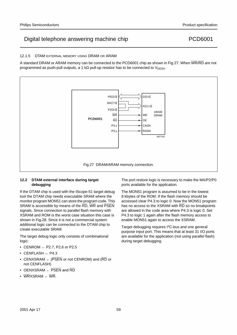
2001 Apr 17 59
Philips Semiconductors Product specification
Digital telephone answering machine chip PCD6001
12.1.5 DTAM EXTERNAL MEMORY USING DRAM OR ARAM
A standard DRAM or ARAM memory can be connected to the PCD6001 chip as shown in Fig.27. When WR/RD are notprogrammed as push-pull outputs, a 1 kW pull-up resistor has to be connected to VDD3V.
handbook, full pagewidth
MGT441
WE
OE
CASN
D[3:0]
A[11:0]
RASN
WR
RD
P3.x
P0[3:0]
MA[7:0]
P2[3:0]
P3.y
PCD6001
ARAMDRAM
Fig.27 DRAM/ARAM memory connection.
12.2 DTAM external interface during targetdebugging
If the DTAM chip is used with the tScope-51 target debugtool the DTAM chip needs executable SRAM where themonitor program MON51 can store the program code. ThisSRAM is accessible by means of the RD, WR and PSENsignals. Since connection to parallel flash memory withXSRAM and ROM is the worst case situation this case isshown in Fig.28. Since it is not a commercial systemadditional logic can be connected to the DTAM chip tocreate executable SRAM.
The target debug logic only consists of combinationallogic:
· CENROM ¬ P2.7, P2.6 or P2.5
· CENFLASH ¬ P4.3
· CENXSRAM ¬ (PSEN or not CENROM) and (RD ornot CENFLASH)
· OENXSRAM ¬ PSEN and RD
· WRXSRAM ¬ WR.
The port restore logic is necessary to make the MA/P2/P0ports available for the application.
The MON51 program is assumed to be in the lowest8 kbytes of the ROM. If the flash memory should beaccessed clear P4.3 to logic 0. Now the MON51 programhas no access to the XSRAM with RD so no breakpointsare allowed in the code area where P4.3 is logic 0. SetP4.3 to logic 1 again after the flash memory access toenable MON51 again to access the XSRAM.
Target debugging requires I2C-bus and one generalpurpose input port. This means that at least 31 I/O portsare available for the application (not using parallel flash)during target debugging.

2001 Apr 17 60
Philips Semiconductors Product specification
Digital telephone answering machine chip PCD6001
handbook, full pagewidth
MGT443
P4.3 CEN
RD OEN
WR WN
RY/BYN
P3.x
P3.z
P1.x
P4.0 to P4.2
P1.6/SCL
P1.7/SDA
P0
P2
EA
PSEN
MA
IO7 to IO0
A18 to A0
A19
DACKN
SCL
SDA
PCD6001
4/8-MbitFLASH
KEILtScope-51
PC
CEN
P0_R
MA_R
P2_R
TX
RX
GND
OEN
WN
IO7 to IO0
A15 to A0
64-kbyteXSRAM
CEN
OEN
IO7 to IO0
A15 to A0
MON51ROM
TARGET DEBUG LOGICAND
OTP PORT RESTORE
I2C-BUS TORS232
CONVERTER
Fig.28 Flash, XSRAM and MON51 ROM memory connection.

2001 Apr 17 61
Philips Semiconductors Product specification
Digital telephone answering machine chip PCD6001
13 THE CODECs
13.1 Definitions
In the description of the CODECs, amplitude units in dBare used. The following definitions apply:
· dBm: used for absolute analog signal power levels.0 dBm equals 1 mW power dissipation in 600 W . Asingle sinewave signal with a power level of 0 dBmcorresponds to an RMS voltage value of 774.6 mV.
· dBmp: used for absolute analog signal power levelswith psophometric weighting according to “CCITTRecommendation G.223”. This unit is used to expressanalog noise power levels.
· dBm0: used for relative digital signal power levels.0 dBm0 is defined in “CCITT Recommendation G.711(Section 4, Table 5)”. It follows that the maximum digitalsignal power level is 3.14 dBm0 (A-law). Thus3.14 dBm0 is the RMS value of a sinewave signal whosepeaks just reach the full-scale of the digital code. For the(internal) bitstream signal (output of ARS and DNS) thepositive full-scale value is a continuous stream of ‘ones’,whereas the negative full-scale value is a continuousstream of ‘zeroes’. For the (internal) digital 14 or 16-bitwords, represented in 2s complement (MSB first) thepositive full-scale value is a ‘zero’ followed by 13 or 15‘ones’, whereas the negative full-scale value is a ‘one’followed by 13 or 15 ‘zeroes’.
· dBm0p: used for relative digital signal power levels withpsophometric weighting according to “CCITTRecommendation G.223”.
· dB: is used for the signal level gain between any twonodes within the speech path. As different signalrepresentations are used within the speech path, thegain value depends on the used signal definitions.
· dBp: is used for the signal level gain between any twonodes within the speech path with psophometricweighting according to “CCITT RecommendationG.223”.
· The uniform PCM reference point is the (virtual) signalnode in the DSP at the input of the PCM encoder for theanalog-to-digital speech path and the output of the PCMdecoder for the digital-to-analog speech path.
13.2 CODEC architecture
The PCD6001 is provided with two CODECs that performthe analog-to-digital and digital-to-analog conversion ofspeech signals. In Fig.29, the CODECs are the interfacebetween the external analog peripherals and the DSP.CODEC1 is used for the line interface and CODEC2 isused for the loudspeaker and the microphone.
The DTCON register bit DTCON.4 selects the input toCODEC1 (LIFMIN1 or LIFMIN2).
The main CODEC functions are (refer to Fig.29):
· AMP - Pre-amplifier
· ARS - Analog Receive Sigma delta ADC
· DDF - Digital Decimation Filter
· DNS - Digital Noise Shaper
· ATD - Analog Transmit DAC.
For CODEC1 the balanced line interface input is fed to theARS block that performs analog-to-digital conversion, thegain of the input can be set to the amplification steps:7, 23 and 35 dB (see Section 17.5 for typical/maximumgain specifications). This programmable range is used bythe microcontroller on command of the DSP to performlimit or automatic gain control. The analog data isconverted by ARS to a bit stream. The basic samplingfrequency (fs) is 8 kHz. The DDF decimates the bit streamdown to 16-bit linear PCM data. The DF has a gain of3.14 dB (which has to be added to the programmable ARSgain) to achieve a uniform reference point at the DSP inputfor linear PCM data. Finally, the DSP will decimate thisdata to 16-bit linear PCM data at a rate of 8 kHz.
The reverse operation is performed in the transmit path.The DSP produces 16-bit linear PCM to the DNS. The ATDwhich is a DAC converts the bit stream into an analogsignal. The converter has a programmable amplificationrange of 18 dB. This programmability is - 12, - 6, +0 and+6 dB.
CODEC2 is built-up in a similar manner as CODEC1, theonly difference being the microphone amplifier before theADC. This will amplify the balanced analog (microphone)signal in the receive path with a fixed +15 dB (seeSection 17.5 for exact gain specifications). For directconnectivity of an external microphone, a software on/offswitchable supply voltage is available.
Several registers are available for the CODECS control:
· DTCON: for selecting the input to CODEC1(DTCON.4 = 0 means LIFMIN1 is selected,DTCON.4 = 1 means LIFMIN2 is selected) and foralternative gain settings (see Section 13.2.2)
· CDVC1: the volume control register for CODEC1
· CDVC2: the volume control register for CODEC2.
· CDTRx: test mode control registers for both CODECS
· PMTRx: test mode control registers for both CODECS

2001 Apr 17 62
Philips Semiconductors Product specification
Digital telephone answering machine chip PCD6001
13.2.1 VOLUME CONTROL REGISTERS (CDVC1 AND CDVC2)
The Volume Control Registers are identical and both are reset to 00H. Table 54 is relevant to both registers.
Table 53 Volume Control Register 1 (SFR address BBH); Volume Control Register 2 (SFR address BCH)
Table 54 Digital-to-analog gain values
Note
1. In these gain values the - 4 dB digital gain (software DSP output port gain of - 2 dB and DNS path gain of - 2 dB) isnot included as in previous PCD600x data sheets.
13.2.2 DATA CONTROL REGISTER (DTCON)
Table 55 Data Control Register (SFR address C7H), reset state 00H
Table 56 Analog-to-digital gain values
Notes
1. The 3.14 dB digital gain of DDF hardware block is not included here. The nominal values given in this table arerounded for naming convention. See Section 17.5 for exact typical/maximum gain specifications.
2. System application should be such that the maximum line input signal level does not exceed the specified value toavoid distortion (see Section 17.5 for maximum input level specifications). At a maximum line input level of - 37 dBmfull-scale control the internal ADC can still be achieved by a maximum gain setting of 35 dB.
3. System application should be such that the maximum differential microphone input signal level does not exceed thespecified value to avoid distortion (see Section 17.5 for maximum input level specifications). At a maximummicrophone input level of - 52 dBm full-scale control the internal ADC can still be achieved by a maximum gain settingof 50 dB. The high dynamic range of the ADC allows for additional digital gain up to 30 dB by the DSP.
4. If the HI_GAIN1/LO_GAIN2 bit is set to logic 1, the value of bit 3 of CDVC1/2 and AMP_EN is overruled and the gainwill be +35 dB for CODEC1 and +7 dB for CODEC2.
7 6 5 4 3 2 1 0
D/A.1 D/A.0 spare spare A/D spare spare spare
CDVC1[7:4]/CDVC2[7:4] DIGITAL-TO-ANALOG GAIN FOR CODEC1 AND CODEC2 (1)
00XX - 12 dB
01XX - 6 dB
10XX 0 dB
11XX +6 dB
7 6 5 4 3 2 1 0
spare spare HI_GAIN1 LINESEL spare AMP_ENA LO_GAIN2 spare
CODEC1 analog-to-digital gain and channel selection CODEC2 analog-to-digital gain
CDVC1[3:0]/CDVC2[3:0]
ANALOG-TO-DIGITAL GAIN (1)
CODEC1 (LINE)(2)CODEC2 (MIC)(3)
HI_GAIN1 (LINE)/LO_GAIN2 (MIC)AMP_ENA = 0 AMP_ENA = 1
0XXX 7 dB 23 dB 38 dB HI_GAIN1/LO_GAIN2 = 0(4)
1XXX 23 dB 35 dB 50 dB
XXXX 35 dB 7 dB HI_GAIN1/LO_GAIN2 = 1(4)

2001 Apr 17 63
Philips Semiconductors Product specification
Digital telephone answering machine chip PCD6001
The analog and digital parts of both CODECs can beindependently activated by the SYMOD register; seeSection 9.2.2. Bit 4 of SYMOD is used to activate themicrophone supply voltage, if the bit is logic 0 the supply isoff.
The balanced microphone input has a minimum differentialinput resistance of RMICDM, and the balanced line interfaceinput has a minimum differential input resistance ofRLIFINDM.
The output resistance of the balanced CODEC outputs isRLIFOUT for CODEC1 and RSPKR for CODEC2 at adifferential output level of 1350 mV (RMS). For exactmeasurement conditions and specified values seeSection 17.5.
handbook, full pagewidth
MGT442
DTCON.4CDVC1
ARS1
ATD1
DDF1
DNS1DT1
DR1
LIFMOUT line interfaceoutput
line interfaceinput
loudspeakeroutput
microphoneinput
receive path
LIFPOUT
LIFMIN1
LIFMIN2LIFPIN
CDVC2
ARS2 AMP
ATD2
DDF2
DNS2DT2
DR2
transmit path
MICP
MICM
SPKRP
SPKRM
CODEC1
CODEC2
DSP
Fig.29 Block diagram of CODECs.

2001 Apr 17 64
Philips Semiconductors Product specification
Digital telephone answering machine chip PCD6001
14 ANALOG VOLTAGE REFERENCE (AVR)
14.1 Bandgap reference
The Analog Voltage Reference circuitry (AVR) includes abandgap circuit with a nominal output voltage of about1.25 V. This voltage is used by the power-on reset blockand by the analog voltage source to generate thereference voltage VREF.
Block AVR is always on, even in System-off mode, and willconsume only a few m A of current. The output of AVR isdirectly connected to the power-on reset block and itdetermines the power-on reset threshold levels accuracyin first order. The connection from AVR to the analogvoltage source circuitry (AVS, see Section 14.2) is via aninternal series resistor of about 500 kW (typical). Thevoltage after this resistor is connected to pin VBGP, whichallows an external capacitor (100 nF) to be connected tofilter out any noise from AVR otherwise entering AVS.
With this configuration the noise at pin VBGP will be about- 115 dBmp. The pin also allows a direct measurement ofthe bandgap voltage, but no current must be drawn.
In order to guarantee a correct start-up of the bandgapvoltage under all conditions, a supply voltage ramp test isperformed on each device. The bandgap voltage iscompared against specified values at the indicated times(see Fig.30). The test setup intends to reflect the worstcase start-up conditions which may occur in an application(for initial power-up and after short power drop). Note thattrise is critical and should not be greater than indicated in agiven application. Other indicated times (tsettle and trise)reflect the worst case conditions for the device andtherefore can change in the application.
handbook, full pagewidth
MGT445tfalltsettle trise
t
measure VBGPVDDA
0 V
0.6 V
2.5 V
tfall = 2 mstsettle = 45 mstrise = 20 ms
Fig.30 Bandgap voltage test setup.

2001 Apr 17 65
Philips Semiconductors Product specification
Digital telephone answering machine chip PCD6001
14.2 Analog Voltage Source (AVS)
The analog voltage source generates the followingvoltages:
· A precise reference voltage VREF. The value in registerVREFR determines the VREF. In the application thisvoltage should be tuned to 2000 mV, since it willdetermine the absolute accuracy of the auxiliaryanalog-to-digital and digital-to-analog conversion. VREFis the direct output of an opamp which can source anoutput current, and not sink. An external capacitorshould be connected between VREF and VSSA forstability and noise performance. The reference voltagecan also directly supply an external electret microphonevia pin VMIC. The switch between VREF and VMIC iscontrolled via bit 4 in the SYMOD special functionregister.
· An analog output voltage DAOUT. This voltage can beset between approximately 8 mV (1 LSB = VREF/256)and VREF (= 2000 mV) by changing the contents ofregister GPDAR. This large range is possible when noopamp is used.
This causes a relatively high output resistance with asettling time of about 10 ms. The dynamic switching ofDAOUT causes the output resistance to be dependentof the actual load on DAOUT. This effect can becancelled if an external capacitor larger than 500 pFbetween DAOUT and VSSA is applied. This will howeverresult in a slower settling time of the output voltage, toabout 30 m s.
· The internal analog common mode voltage Vacm, usedin the CODEC.
· The internal voltage Vadc is used only when ananalog-to-digital conversion is executed.
As mentioned above, for highest analog performance thereference voltage VREF has to be adjusted in theapplication to 2000 mV. For this purpose the VREFR SFRhas been defined. The reset state should ensure that thereference voltage is about 2000 mV on a typical device.Exact adjustment has to be done under software controlusing the VREFR register, where increasing the VREFRvalue will decrease the reference voltage.
14.2.1 VOLTAGE REFERENCE REGISTER (VREFR)
Table 57 Voltage Reference Register (SFR address BAH); reset state A0H
7 6 5 4 3 2 1 0
VREF.7 VREF.6 VREF.5 VREF.4 VREF.3 VREF.2 VREF.1 VREF.0

2001 Apr 17 66
Philips Semiconductors Product specification
Digital telephone answering machine chip PCD6001
15 IOM
15.1 Features
The IOM block in the PCD6001 is a 4-wire serial interfaceperforming following functions:
· Digital interface with up to two 64 kbits/s channels at abit rate of n ´ 256 kbits/s (n = 1, 2, 3, 4 or 8), complyingwith the “IOM-2 specifications” (IOM-2 is a registeredtrademark of Siemens AG)
· Digital interface with 32 slots/frame and non-doubleddata clock; compatible with the digital interface of somespeech CODEC ICs
· Autonomous storing/fetching of data into/from theDSP I/O registers
· Byte or word (16 bits) transfer.
15.2 Pin description
The following pins are used by the IOM interface:
· DI: serial data input with a bit rate of n ´ 256 kbits/s(n = 1, 2, 3, 4 or 8)
· DO: serial data output with a bit rate of n ´ 256 kbits/s(n = 1, 2, 3, 4 or 8)
· FSC: 8 kHz frame synchronization input/output
· DCK: data clock input/output. Twice the datatransmission frequency on DI and DO, except in thenon-doubled data clock mode (see Section 15.3).
These pins are alternative functions of P3. Whenactivated, DO is an open-drain pin, as many devices mustbe able to write on the same data line in a time-multiplexedmode. Therefore DO must be externally pulled-up. FSCand DCK are inputs or push-pull outputs, depending on theIOM being in Slave or Master mode. Activation of the IOMalternative functions of P3 and switching between Slave orMaster mode is controlled by the SFR ALTP, bit 6 and 5respectively (see Section 16.2 for more details).
15.3 Functional description
The digital interface of the PCD6001 can work at severalbit rates, summarized in Table 61. A particular bit rate isselected by writing the 3-bit code given in the first columnof the table into the IOM control register bits IOMC[15:13].Choosing the code ‘000’ or ‘001’ deactivates the IOMinterface and stops all the transactions on the IOM bus.This is the default state after reset.
The PCD6001 IOM can be master or slave. After reset theIOM is in Slave mode. Switching between Slave or Mastermode is controlled by the SFR ALTP, bit 6 and bit 5respectively (see Section 16.2.5 for more details). In Slavemode both FSC and DCK are inputs. In Master mode bothFSC and DCK are outputs. In Master mode FSC and DCKare generated by the TICB (see Section 9.1). Master modeshould only be used in combination with the bit rate768 kbits/s. Slave mode should only be used whenoperating with a 3.456 MHz (or multiple) crystal. Ingeneral, proper IOM functionality is only guaranteedat DSP operating frequencies of 28 and 42 MHz.
FSC is an 8 kHz framing signal for synchronizing datatransmission on DI and DO. The rising edge of FSC givesthe time reference for the first bit transmitted in the first slotof a speech frame. The number of slots per speech framedepends on the selected data rate. Each slot contains8 data bits.
DCK is a data clock. Its frequency is twice the selecteddata rate in IOM mode. In speech mode, theDCK frequency is equal to the data rate (2048 kHz for2048 kbits/s).
DI is the serial data input. Data coming on DI in packets of8 bits (A-law PCM encoded data) or 16 bits (linear PCMdata) is stored temporarily in an IOM data buffer, fromwhere it is processed by the on-chip DSP. On the otherhand, data written into the IOM data buffers by the DSP isshifted out on pin DO.
There are two IOM data buffers, allowing the use of two8-bit channel. One channel is 64 kbits/s in case of A-lawPCM encoded data and 128 kbits/s if linear PCM data istransferred, in which case two consecutive slots are used.
The speech mode was implemented to support the Codecinterface of some speech compression ICs. This mode isvery similar to the IOM 32 slots mode, the main differencebeing the non-doubled data clock. See Section 15.6 fortiming information.
15.4 IOM data buffers
Table 58 and 59 show the two 16-bit DSP registers usedas data buffers: IOMDI for storing inbound data andIOMDO for the outbound data. The high bytes store thedata of buffer 1, the low bytes the data of buffer 0.

2001 Apr 17 67
Philips Semiconductors Product specification
Digital telephone answering machine chip PCD6001
15.4.1 IOM DATA IN REGISTER (IOMDI)
Table 58 IOM Data In Register; reset state 00H
15.4.2 IOM DATA OUT REGISTER (IOMDO)
Table 59 IOM Data Out Register; reset state 00H
15.5 IOM Control Register (IOMC)
The bit rates, the selection of active slots on the IOM interface and the logic connection between an IOM slot and an IOMdata buffer are defined in the IOM Control Register. The IOM modes which can be selected are listed in Table 61.
Writing to the IOMC register is done via the Application Programming Interface (API) software. Please refer to the APIspecification for more details.
Table 60 IOM Control Register; reset state 00H
Table 61 Selection of IOM modes
Note
1. The Speech mode is similar to the IOM slave 32 slots mode, but with a non-doubled data clock DCK.
15 14 13 12 11 10 9 8 7 6 5 4 3 2 1 0
IOM inbound data buffer 1 IOM inbound data buffer 0
15 14 13 12 11 10 9 8 7 6 5 4 3 2 1 0
IOM outbound data buffer 1 IOM outbound data buffer 0
15 14 13 12 11 10 9 8 7 6 5 4 3 2 1 0
IOM Mode select IOM buffer 0; slot position spare buffer 0active
buffer 1active
IOM buffer 1; slot position
IOMC[15:13] MODE
000 or 001 Inactive (default after reset)
010 IOM Slave mode, 256 kbits/s in 4 slots/speech-frame
011 IOM Slave mode, 512 kbits/s in 8 slots/speech-frame
100 IOM Master/Slave mode, 768 kbits/s in 12 slots/speech-frame
101 IOM Slave mode, 1024 kbits/s in 16 slots/speech-frame
110 Speech Slave mode, 2048 kbits/s in 32 slots/speech-frame(1)
111 IOM Slave mode, 2048 kbits/s in 32 slots/speech-frame

2001 Apr 17 68
Philips Semiconductors Product specification
Digital telephone answering machine chip PCD6001
15.6 Timing
The timing on the 4-wire interface is given in Fig.31 and Table 62 for the IOM mode and in Fig.32 and Table 63 for thespeech mode.
handbook, full pagewidth
MGM794
DCK
FSC
DI/DO
DCK
FSC
DO
DI
bit 7 bit 6 bit 5
tr(DCK) tf(DCK)
td(F)
tWH
td(DF)
td(DC)
tsu(F)
th(D)
tsu(D)
tw(FH)
tWLTDCK
bit 7
bit 7
Fig.31 4-wire interface timing in IOM mode.

2001 Apr 17 69
Philips Semiconductors Product specification
Digital telephone answering machine chip PCD6001
Table 62 Timing parameters in IOM mode
Notes
1. Corresponds to the highest DCK frequency allowed (4.096 MHz) with a 10% margin.
2. Condition CL = 150 pF.
SYMBOL PARAMETER MIN. MAX. UNITS
tr(DCK) data clock rise time - 60 ns
tf(DCK) data clock fall time - 60 ns
TDCK data clock period 220(1) - ns
tWH data clock HIGH time pulse width 80 - ns
tWL data clock LOW time pulse width 80 - ns
tr(FSC) frame sync rise time - 60 ns
tf(FSC) frame sync fall time - 60 ns
td(FSC) frame sync delay time - tWL 60 ns
tsu(FSC) frame sync set-up time 60 - ns
tWFH frame sync HIGH time pulse width 130 - ns
td(DC) output data to data clock delay time - 100(2) ns
td(DF) output data to frame sync delay time - 150(2) ns
tsu(D) input data set-up time tWH - ns
th(D) input data hold time 50 - ns

2001 Apr 17 70
Philips Semiconductors Product specification
Digital telephone answering machine chip PCD6001
Table 63 Timing parameters in speech mode
Notes
1. Corresponds to the DCK frequency (2.048 MHz) with a 10% margin.
2. Condition CL = 150 pF.
SYMBOL PARAMETER MIN. MAX. UNITS
td(FSC) frame sync (FSC) delay time - tWL 100 ns
tsu(FSC) frame sync (FSC) set-up time 60 - ns
tWFH frame sync (FSC) high time pulse width 130 - ns
TDCK data clock (DCK) period 440(1) - ns
tWH data clock (DCK) high time pulse width 150 - ns
tWL data clock (DCK) low time pulse width 150 - ns
td(DC) output data (DO) to data clock delay time - 100(2) ns
tsu(D) input data (DI) set-up time 60 - ns
th(D) input data (DI) hold time 60 - ns
handbook, full pagewidth
FSC
DCK
DI/DO
FSC
DCK
DO B7
B7
B6
DI
B2 B1 B0B5 B4 B3B6B7
tW(FH)
TDCK
tsu(FSC)
th(D)tsu(D)
tWH tWL
td(FSC)
td(DC)
MGM795
Fig.32 4-wire interface timing in speech mode.

2001 Apr 17 71
Philips Semiconductors Product specification
Digital telephone answering machine chip PCD6001
16 EXTERNAL I/O INTERFACES
16.1 External analog interfaces
16.1.1 GENERAL PURPOSE ADC AND DAC
For general use, for instance battery management, parallelset detection or speaker amplifier volume control, a 2-linemultiplexed 8-bit ADC and an 8-bit DAC are on-chip. TheADC and the DAC consist of several analog sub-blockscalled AVS and AAD, which are controlled by the digitalblock DCA (see Fig.33). Block AVS generates voltages ina time multiplexed way, and acts as a DAC with thebandgap voltage VBGP as input voltage. Block AADcontains a comparator that is part of the successiveapproximation ADC formed by a combination of AVS, AADand DCA. The analog-to-digital conversion can beperformed on two external input signals: AD0IN andAD1IN.
The whole circuit is active as long as the chip is inSystem-on mode. Both the ADC and the DAC can becontrolled by the microcontroller, the SFR mapped
DCA block allowing the user a flexible interface to analogperipherals.
16.1.2 GENERAL PURPOSE ADC
The on-chip ADC is a two channel multiplexed 8-bitconverter. The control of this converter is done via two bitsin the microcontroller GPADC SFR. One bit selects thechannel and the other bit is the converter request bit. Therequest bit is reset by hardware when the converter hasfinished its conversion cycle. The ADC (AAD in Fig.33), isof the successive approximation type.
An internal register contains the value of the slider positionand is changed after each comparison of Vadc with one ofthe two possible analog-to-digital inputs (AD0IN andAD1IN). After 8 comparisons the conversion is finishedand the contents of the internal register is copied into theregister GPADR. Total analog-to-digital conversion time(from setting the Request bit until GPADR ready) is lessthan 50 ms. This register can in turn be read by the internalmicrocontroller.
16.1.2.1 General Purpose ADC Register (GPADC)
Table 64 General Purpose ADC Register (SFR address C3H); reset state 00H
Table 65 Description of GPADC bits
16.1.2.2 General Purpose ADC Result Register (GPADR)
This register holds the 8-bit result value from the conversion. The conversion range is 0 to 2000 mV (VREF) with 8 mVresolution.
Table 66 General Purpose ADC Result Register (SFR address C2H); reset state 00H, read only
7 6 5 4 3 2 1 0
- - - - - AADC CS REQCOM
BIT SYMBOL DESCRIPTION
7 to 3 - These 5 bits are reserved.
2 AADC Automatic Analog-to-Digital Conversion. If AADC = 1, then a conversion isperformed every 30 ms, regardless of state of request confirm bit.
1 CS Channel Select. If CS = 0, analog-to-digital conversion input is on pin AD0IN. If CS = 1,analog-to-digital conversion input is on pin AD1IN. Switching of the analog-to-digitalchannel is only allowed when no analog-to-digital conversion currently is in progress.Otherwise the resulting value will be corrupt.
0 REQCOM Request Confirm.
7 6 5 4 3 2 1 0
A/D.7 A/D.6 A/D.5 A/D.4 A/D.3 A/D.2 A/D.1 A/D.0

2001 Apr 17 72
Philips Semiconductors Product specification
Digital telephone answering machine chip PCD6001
16.1.3 GENERAL PURPOSE DAC
The on-chip DAC is a single channel 8-bit converter. The control of this converter is done via the GPDAR register. Thevalue written in this register triggers the conversion which will be present at the output pin after the digital-to-analogconversion cycle (<25 m s). The range from the digital-to-analog output is 0 to 2000 mV (VREF).
The conversion principle for both analog-to-digital and digital-to-analog conversion is shown in Fig.34.
16.1.3.1 General Purpose DAC Register (GPDAR)
Table 67 General Purpose DC A Register (SFR address C4H); reset state 80H
7 6 5 4 3 2 1 0
D/A.7 D/A.6 D/A.5 D/A.4 D/A.3 D/A.2 D/A.1 D/A.0
handbook, full pagewidth
MGM796
VACMRDAC
VADC
AVS
AAD
SYMOD.4 (MIC supply bit)
VMIC
Vref
DAOUT
AD0IN
AD1IN
VREFRDCA GPADC GPDAR GPADR
GPADC(channelrequest bit)
VBGP
Fig.33 The architecture of the auxiliary DAC and ADC.
handbook, full pagewidth
MGM797
time
pin GPDARrepresents output
GPADC SFRhas been changedby the microcontroller
GPADC SFRhas been changedby the micro
HW resets request bit.Conversion finished.Result in GPADR SFR
conversion cycle (<30 m s)
analog-to-digital conversion
conversion cycle (<10 m s)
digital-to-analog conversion
Fig.34 Analog-to-digital and digital-to-analog conversion principle.

2001 Apr 17 73
Philips Semiconductors Product specification
Digital telephone answering machine chip PCD6001
16.2 External digital Interfaces
For control of peripherals like a display, ringer, key padand line interface a large number of general purposedigital I/O pins are available in addition to the flashmemory, LCD control pins and MSK or IOM modem pins.The exact number of free I/O pins depends on the choiceof peripherals that make up the system configuration. Incase all alternative port functions of P1 and P3 are used,10 input lines remain available on P1 and P3 of which 7are programmable for interrupts.
I/O ports P1 and P3 are ‘weak pull-up’ types which cantherefore be used either as inputs or outputs. The resetvalue of P1 and P3 is FFH (input mode). In output modefor driving with a logic 1 (weak pull-up) the external load ofP1 and P3 should be equivalent to >100 kW , for ‘driving’with a logic 0 the sink current should not exceed 4 mA.
In addition to P1 and P3 there are 16 output portsavailable at P2 and MA. Output Ports P2 and MA arepush-pull ports and their reset value is 00H (output 00H).The driving level of P2 and MA is 4 mA for either logic 0 orlogic 1. Port P4 provides the flash memory and displaycontrol signals. The P1, P3 and P4 I/O lines are availableas SFR bit-addressable I/O registers in the configurationshown in Fig.35, while P2 and MA are available as (not bitaddressable) XDATA mapped ports (for exactconfiguration and detailed description see Chapter 12).
The MA and P2 ports are described in Chapter 12. Theconfiguration of Ports P1 and P3 are described in theTables 68 to 76.
MGM798
MA00
MA11
MA22
MA33
MA44
MA55
MA66
MA77
MA
P000
P011
P022
P033
P044
P055
P066
P077
P0
P1.0/EX20
P1.1/EX31
P1.2/EX42
P1.3/EX53
P1.4/EX64
P1.55
P1.6/SCL6
P1.7/SDA7
P1
P2.00
P2.11
P2.22
P2.33
P2.44
P2.55
P2.66
P2.77
P2
P3.0/MOUT0/DO0
P3.1/MOUT1/DCK1
P3.2/EX0N2
P3.3/EX1N3
P3.4/T04
P3.5/T15
P3.6/MOUT2/FSC6
P3.7/MIN/DI7
P3
P4.0/LE0
P4.1/FSK1
P4.2/FSO2
P4.33
P4.4/FSI4
P4.5/GPC5
P4
Fig.35 DTAM general purpose digital I/Oconfiguration.

2001 Apr 17 74
Philips Semiconductors Product specification
Digital telephone answering machine chip PCD6001
16.2.1 PORT 1 REGISTER (P1)
The alternative outputs (SDA and SCL) are connected with the general purpose outputs via an AND logic gate. Thereforewhen using the alternative functions the corresponding port bits have to be set to a logic 1.
For control of I2C-bus peripherals like for instance EEPROMs and LCD displays, P1.6 and P1.7 can also be used as SDAand SCL to support I2C-bus. See Section 10.11 on how to activate this alternative function of P1.6 and P1.7. The rest ofPort 1 is defined as general purpose I/O pins as for the standard 80C51 microcontroller.
Table 68 Port 1 Register (SFR address 90H); bit addressable; reset state FFH
Table 69 P1 pin configuration
16.2.2 PORT 3 REGISTER (P3)
Port 3 is defined as a set of 8 general purpose I/O pins similar to the standard 80C51 microcontroller except for P3.6 andP3.7 which do not have the RD and WR functionality (the RD and WR are separate pins). Table 72 gives the differentfunctions and the corresponding port configurations available on P3.7, P3.6, P3.1 and P3.0. The last column gives thefunction and configuration after reset.
Table 70 P3 (B0H) bit assignment; bit addressable; reset state FFH; note 1
Note
1. The alternative outputs (for MSK, IOM) are connected with the general purpose outputs via an AND logic gate.Therefore when using the alternative functions the corresponding port bits have to be set to a logic 1.
Table 71 P3 pin configuration
Table 72 Port 3.7, 3.6, 3.1 and 3.0 modes and configuration
7 6 5 4 3 2 1 0
P1.7/SDA P1.6/SCL P1.5 P1.4/EX6 P1.3/EX5 P1.2/EX4 P1.1/EX3 P1.0/EX2
PORT PINS CONFIGURATION
P1.7 and P1.6 open-drain
P1.5 to P1.0 quasi-bidirectional
7 6 5 4 3 2 1 0
P3.7/MIN/DI P3.6/MOUT2/FSC
P3.5/T1 P3.4/T0 P3.3/EX1N P3.2/EX0N P3.1/MOUT1/DCK
P3.0/MOUT0/DO
PORT PINS CONFIGURATION
P3.7, P3.6, P3.1 and P3.0 see Table 72
P3.5 to P3.2 quasi-bidirectional
MSKIOM GENERAL PURPOSE I/O PORT
(RESET STATE)SIGNAL MASTER SLAVE
MOUT0 push-pull DO open-drain 4 mA open-drain 4 mA P3.0 quasi-bidirectionalweak pull-upMOUT1 push-pull DCK push-pull input P3.1
MOUT2 push-pull FSC push-pull input P3.6
MIN input DI input input P3.7

2001 Apr 17 75
Philips Semiconductors Product specification
Digital telephone answering machine chip PCD6001
16.2.3 PORT 4 REGISTER (P4)
The alternative outputs (GPC, FSO, FSK and LE) are connected with the general purpose outputs via an AND gate.Therefore, when using the alternative functions the corresponding port bits should be set to a logic 1.
Table 73 Port 4 Register (SFR address 98H); bit addressable; reset state 1EHH; note 1
16.2.4 PORT 4 CONFIGURATION REGISTER (P4CFG)
This register is used to select the output configuration of the pins WR, RD and P4.0 to P4.4. The output configuration isopen-drain by default after reset. Note that the output configuration of P4.5 is selected by the P4.5 bit in SFR ALTP.
Table 74 Port 4 Configuration Register (SFR address 9FH); reset state 00H
Table 75 Description of P4CFG bits
16.2.5 ALTERNATIVE PORT FUNCTION REGISTER (ALTP)
This register selects the pin configuration for the MSK, IOM master/slave and general purpose function; see Table 77.The general purpose clock function is described in Section 9.1. The LE functionality is described in Section 10.13.
Table 76 Alternative Port Function Register (SFR address ABH); reset state 00H
Table 77 P3.7, P3.6, P3.1 and P3.0 selection of pin configurations for alternative function
7 6 5 4 3 2 1 0
- - P4.5/GPC P4.4/FSI P4.3 P4.2/FSO P4.1/FSK P4.0/LE
7 6 5 4 3 2 1 0
WR RD EAM P4.4 P4.3 P4.2 P4.1 P4.0
BIT SYMBOL DESCRIPTION
7 WR If WR = 0, then open-drain configuration. If WR = 1, then push-pull configuration.
6 RD If RD = 0, then open-drain configuration. If RD = 1, then push-pull configuration.
5 EAM The EAM bit is used to select the Enhanced Addressing Mode; this is described in moredetail in Chapter 12.
4 P4.4 If P4.4 = 0, then open-drain configuration. If P4.4 = 1, then push-pull configuration.
3 P4.3 If P4.3 = 0, then open-drain configuration. If P4.3 = 1, then push-pull configuration.
2 P4.2 If P4.2 = 0, then open-drain configuration. If P4.2 = 1, then push-pull configuration.
1 P4.1 If P4.1 = 0, then open-drain configuration. If P4.1 = 1, then push-pull configuration.
0 P4.0 If P4.0 = 0, then open-drain configuration. If P4.0 = 1, then push-pull configuration.
7 6 5 4 3 2 1 0
- IOM on P3 IOM master/MSK
P4.5 GPC off/on GPC source LE off/on early LE
ALTP.6 ALTP.5 MODE
0 0 general purpose I/O port
0 1 MSK
1 0 IOM slave
1 1 IOM master

2001 Apr 17 76
Philips Semiconductors Product specification
Digital telephone answering machine chip PCD6001
17 ELECTRICAL CHARACTERISTICS
17.1 Limiting valuesIn accordance with the Absolute Maximum Rating System (IEC 60134); note 1
Note
1. Parameters are valid over operating temperature range unless otherwise specified; all voltages are with respect toVSS unless otherwise specified.
SYMBOL PARAMETER MIN. MAX. UNIT
VDD3V supply voltage 3.0 V (VDD3V2 and VDD3V3) - 0.5 +3.6 V
VDD2.5V supply voltage 2.5 V (VDD3V1, VDDA, VDDPLL) - 0.5 +3.3 V
VI input voltage on any pin with respect to ground (VSS) - 0.5 VDD + 0.5 V
II/O maximum sink/source current for all input/output pins - 10 +10 mA
IVDD, IVSS maximum DC current for each supply pin - 150 mA
Ptot total power dissipation - 800 mW
VESD(HBM) maximum ESD stress level applied; according to human bodymodel (100 pF; 1.5 kW )
- 1500 V
VESD(MM) maximum ESD stress level applied; according to machine model(200 pF; 0.75 m H)
- 150 V
Tamb operating ambient temperature - 25 +70 °CTstg storage temperature - 65 +150 °C

2001 Apr 17 77
Philips Semiconductors Product specification
Digital telephone answering machine chip PCD6001
17.2 Supply characteristics
Notes
1. This defines requirements for the external Power-on reset circuit. The exact requirements can be relaxed dependingon the specific application. A hysteresis is required to overcome reset oscillations especially in battery operatedapplications.
2. For these parameters, the recommended external components are specified which are supported by the internaloscillator. This is not measured on a sample-by-sample basis.
SYMBOL PARAMETER CONDITIONS/REMARKS MIN. TYP. MAX. UNIT
VDD3V1 digital supply voltage to pinsVDD3V1
2.25 2.5 2.75 V
VDD3V2/3 digital supply voltage to pinsVDD3V2 and VDD3V3
voltage must be set equal or higherthan VDD3V1
2.25 3.0 3.3 V
VDDA analog supply voltage to pinVDDA
2.25 2.5 2.75 V
VDDPLL analog supply voltage to pinVDDPLL
2.25 2.5 2.75 V
IDD(max) total input current whenrecording a message fromPSTN, CAS, line echocancellation, listen in onCODEC2 to all supply pins
PLL on; CODEC1 and CODEC2active; DSP at 42 MHz; microcontrollerat 21 MHz;VDD3V1 = VDDA = VDDPLL = 2.75 V;VDD3V2 = VDD3V3 = 3.30 V; no load
- 28 35 mA
VDD3V1 only - 22.0 - mA
VDD3V2 only no load on port pins - 0.01 - mA
VDD3V3 only no load on port pins - 0.01 - mA
VDDA only - 5.0 - mA
VDDPLL only - 0.5 - mA
IDD(POTS) POTS mode supply currentto all supply pins
PLL off; DSP only generating DTMFtones; only CODEC1 D/A on;microcontroller in power-down;XTAL runs at 3.58 MHz; PMTR2.0 = 1;CDTR2.0 = 1;VDD3Vx = VDDA = VDDPLL = 2.25 V;no load
- 2.6 3.5 mA
IDD(sys-off) total input current when inSystem-off mode
digital-to-analog part of CODEC1 andCODEC2 switched-off
- 0.17 0.90 mA
POR (Power-on reset)
Vth(H) POR threshold value HIGH note 1 - - 2.2 V
Vth(L) POR threshold value LOW note 1 1.8 - - V
Vhys POR hysteresis note 1 0.08 - - V
OSC
CL(xtal1,2) crystal load capacitances atXTAL1 and XTAL2 to VSS
3.45 to 13.824 MHz; note 2 - 18 39 pF
RS crystal series resistance 3.58 MHz; note 2 - - 300 W13.824 MHz; note 2 - - 40 W
CP crystal shunt capacitance note 2 - - 7 pF

2001 Apr 17 78
Philips Semiconductors Product specification
Digital telephone answering machine chip PCD6001
17.3 Digital I/O
Notes
1. VDD(periph) refers to the peripheral supplies VDD3V2 and VDD3V3.
2. VDD - VOUT = 400 mV (for IOH), VOUT - VSS = 400 mV (for |IOL|).3. 4 mA drive levels are only guaranteed for VDD3V2/3 greater than 2.7 V.
4. On a LOW-to-HIGH transition, the output current value will be 4 mA for one microcontroller clock period, beforechanging to the specified lower value. VDD3Vx = VDDA = VDDPLL = 2.75 V.
5. If the MSK mode is activated, the output current value for P3.0, P3.1 and P3.6 will continuously be 4 mA. If the IOMMaster mode is activated, the output current value for P3.1 and P3.6 will continuously be 4 mA.
6. When configured as push-pull.
SYMBOL PARAMETER CONDITIONS MIN. MAX. UNIT
VIL LOW-level input voltage
SDA and SCL 0 0.3VDD3V1 V
other pins note 1 0 0.2VDD(periph) V
VIH HIGH-level input voltage
SDA and SCL 0.7VDD3V1 VDD(periph) V
other pins note 1 0.8VDD(periph) VDD(periph) V
|IOL| LOW-level output current notes 2 and 3
RD, WR, PSEN, P0, P1, P2, P3,P4 and MA
4 - mA
IOH HIGH-level output current notes 2 and 3
RD(6), WR(6), PSEN, P0, P2,P4(6) and MA
- mA
P1.0, P1.1, P1.2, P1.3, P1.4,P1.5 and P3
90(4)(5) 250(4)(5) m A
Iload Total static load current on VDD3V2/VDD3V3 - 30 mA

2001 Apr 17 79
Philips Semiconductors Product specification
Digital telephone answering machine chip PCD6001
17.4 Analog supplies and general purpose ADC and DAC
Notes
1. VBGP output current is zero. Decoupling capacitance between VBGP and VSSA is 100 nF.
2. The VREF output current is zero however the VREF output buffer is loaded via VMIC (see note 3). Decouplingcapacitance between VREF and VSSA is between 1 and 100 m F, with a 100 nF capacitance in parallel. The output canonly source current (i.e. not sink).
3. Pin VMIC is connected to VREF via an internal switch. The VMIC switch is closed by setting SYMOD.4 = 1. The VMICDC output current is max. 400 m A, and VREF must be programmed to its typical value. For the connections of VMIC toa microphone (see Fig.36). VMIC adjustment can only be done by adjusting VREF.
4. Output resistances represent the theoretical maximum which can be guaranteed by design. Actual output resistancevalues can vary depending on several conditions as processing, temperature and drive signal shape.
SYMBOL PARAMETER CONDITIONS MIN. TYP. MAX. UNIT
VBGP AVR bandgap voltage note 1 1.15 1.23 1.30 V
VREF(RESET) reference voltage, after reset note 2 1.9 2.0 2.1 V
VREF(TUNED) reference voltage when tuned viaVREFR
- 30 - mV
dVMIC VREF - VMIC note 3 - 40 - mV
VADIN,OFS ADIN1 and ADIN2 input offsetvoltage
- 20 50 mV
VADIN1,2 ADIN1 and ADIN2 input voltagerange
0 - VREF mV
RADIN1,2 ADIN1 and ADIN2 inputresistance
2 10 - MW
RDAOUT DAOUT output resistance note 4 - 7 - kWVDAOUT DAOUT output voltage range 8 - VREF mV

2001 Apr 17 80
Philips Semiconductors Product specification
Digital telephone answering machine chip PCD6001
17.5 CODECsFor all values specified, VREF is tuned to 2.0 V; unless mentioned differently, typical values for the analog-to-digital anddigital-to-analog filter characteristics conform to the G.712 specification.
SYMBOL PARAMETER CONDITIONS MIN. TYP. MAX. UNIT
Analog-to-digital path performance
VMIC maximum microphone input level notes 1 and 2 - - - 8 dBm
RMIC(DM) microphone input resistance fromMICM to MICP, differential mode
notes 3 and 4 - 250 - kW
RMIC(CM) microphone input resistance fromMICM to VSSA or MICP to VDDA,common mode
notes 3 and 5 - 25 - kW
VLIFIN(max) maximum line input level notes 1 and 6 - - - 8 dBm
RLIFIN1(dif) line input resistance from LIFMIN1 toLIFPIN, differential mode
notes 3 and 7 - 1000 - kW
RLIFIN1(CM) minimum line input resistance fromLIFMIN1 to VSSA or LIFPIN to VDDA,common mode
notes 3 and 8 - 25 - kW
RLIFIN2(dif) minimum line input resistance fromLIFMIN2 to LIFPIN, differential mode
notes 3 and 9 - 50 - kW
RLIFIN2(CM) minimum line input resistance fromLIFMIN2 to VSSA, common mode
notes 3 and 10 - 1000 - kW
G(A/D)(7dB) typical analog-to-digital path gain ofCODEC1/ CODEC2 from LIF/MIC toDR1/DR2
notes 1 and 11 - 7.1 - dB
G(A/D)(23dB) notes 1 and 12 - 23.5 - dB
G(A/D)(35dB) notes 1 and 13 - 35.5 - dB
G(A/D)(preamp) additional path gain for CODEC2microphone preamplifier
notes 1 and 14 - 14.5 - dB
D G(A/D)(7dB/23dB) delta analog-to-digital path gain ofCODEC1/ CODEC2 from LIF/MIC toDR1/DR2
notes 1 and 15 - 1 0 1 dB
D G(A/D)(35dB) notes 1 and 16 - 1.5 0 1.5 dB
F(A/D)(idle) analog-to-digital idle channel noise notes 1 and 17 - - 85 - 75 dBm0p
S/(N+THD)(A/D)( - 25) analog-to-digital signal-to-(noise + totalharmonic distortion) ratio for CODEC2at 23 dB gain
notes 1 and 18 - 76 - dBp
S/(N+THD)(A/D)( - 49) notes 1 and 19 40 52 - dBp
S/(N+THD)(A/D)( - 65) notes 1 and 20 - 36 - dBp
S/(N+THD)(A/D)( - 9) analog-to-digital signal-to-(noise + totalharmonic distortion) ratio for CODEC1at 7 dB gain
notes 1 and 21 - 78 - dBp
S/(N+THD)(A/D)( - 25) notes 1 and 22 - 62 - dBp
S/(N+THD)(A/D)( - 49) notes 1 and 23 24 38 - dBp
td(g)(A/D) analog-to-digital path group delay - 500 - m s
Digital-to-analog path performance
VLIFOUT(dif) maximum line interface differentialoutput level
note 24 - 1400 - mV
RLIFOUT line interface output resistance note 25 - 20 - WVSPKRD maximum speaker differential output
levelnote 26 - 1400 - mV
RSPKR speaker output resistance note 25 - 8 - W

2001 Apr 17 81
Philips Semiconductors Product specification
Digital telephone answering machine chip PCD6001
Notes
1. For the definition of the amplitude units (dB, dBm, dBm0, dBmp, dBm0p) see Section 13.1. All measurements areperformed with chopping switched on (PMTR2 = 04H) and unless mentioned otherwise, all measurements areperformed in RTC mode = 0 (CKCON.6 = 0) and at nominal supply voltage (VDDA = 2.50 V).
2. Maximum sinewave RMS level applied differentially between pins MICP and MICM. The analog-to-digital path gainfor CODEC2 is set to 7 dB (DTCON.1 = 1, DTCON.2 = 0). For larger input levels the output signal will saturate. Forhigher analog-to-digital gain settings (including the microphone preamplifier), the maximum RMS input level willdecrease by the same amount as the gain will increase.
3. All input resistances represent the theoretical minimum which can be guaranteed by design. Note that given inputresistance values can vary depending on several conditions as processing, temperature and input signal shape. Forthe measurement, the input signal is a 1 kHz sine wave which is AC coupled with a 1 m F capacitor (see Applicationexample in Fig. 36). The input resistance will increase when others than the noted gains are selected. For detailedinformation on input resistances for all gain settings, refer to the PCD6001 application note which is available.
4. The differential resistance is seen between pins MICP and MICM. The minimum resistance will be seen for ananalog-to-digital path gain of 7 dB and will slightly increase for all other gain settings.
5. The common mode resistance is seen between MICP/MICM and VSSA. MICP and MICM are shorted. It correspondsto RMICVDD ||RMICVSS (see Fig.36). The minimum resistance will be seen for an analog-to-digital path gain of23/35 dB and will increase for all other gain settings.
6. Maximum sinewave RMS level applied differentially between pins LIFPIN and LIFMIN1/LIFMIN2. VREF is tuned to2.0 V and the analog-to-digital path gain for CODEC1 is set to 7 dB (CDVC1.3 = 0, DTCON.5 = 0). For larger inputlevels the output signal will saturate. For higher analog-to-digital gain settings, the maximum RMS input level willdecrease by the same amount as the gain will increase.
7. The differential resistance is seen between pins LIFPIN and LIFMIN1. The minimum resistance will be seen for ananalog-to-digital path gain of 23/35 dB and will increase for other gain settings.
8. The common mode resistance is seen between LIFPIN/LIFMIN1 and VSSA. LIFPIN and LIFMIN1 are shorted. Itcorresponds to RLIF1VDD || RLIF1VSS (see Fig.36). The minimum resistance will be seen for an analog-to-digital pathgain of 7 dB and will increase for other gain settings.
9. The differential resistance is seen between pins LIFPIN and LIFMIN2. The minimum resistance will be seen for ananalog-to-digital path gain of 23/35 dB and will increase for other gain settings.
10. The common mode resistance is seen between LIFPIN/LIFMIN2 and VSSA. LIFPIN and LIFMIN2 are shorted.It corresponds to RLIF2VDD || RLIF2VSS (see Fig. 36). The minimum resistance will be seen for an analog-to-digital pathgain of 7 dB and will increase for other gain settings.
11. Absolute typical gain for CODEC1 and CODEC2 for gain step 7dB (CDVC1.3 = 0, DTCON.5 = 0 and DTCON.1 = 1),measured at the DR1/DR2 bitstream interface as defined in Fig.29 using a 1020 Hz sinewave. VREF is tuned to2.00 V.
12. Absolute typical gain for CODEC1 and CODEC2 for gain step 23 dB (CDVC1.3 = 1, CDVC2.3 = 0 and DTCON.5 = 0,DTCON.1 = 0), measured at the DR1/DR2 bitstream interface as defined in Fig.29 using a 1020 Hz sinewave. VREFis tuned to 2.00 V.
D G(D/A) delta digital-to-analog path gain fromDT1/DT2 to SPKR or LIFOUT
notes 1 and 27 - 1 0 1 dB
F(D/A)(idle) digital-to-analog idle channel noise notes 1 and 28 - - 89 - 80 dBmp
S/(N+THD)(D/A)(0) digital-to-analogsignal-to-(noise + totalharmonic distortion) ratio
notes 1 and 29 - 80 - dBp
S/(N+THD)(D/A)( - 40) notes 1 and 30 - 42 50 - dBp
td(g)(D/A) digital-to-analog path group delay - 500 - m s
SYMBOL PARAMETER CONDITIONS MIN. TYP. MAX. UNIT

2001 Apr 17 82
Philips Semiconductors Product specification
Digital telephone answering machine chip PCD6001
13. Absolute typical gain for CODEC1 and CODEC2 for gain step 35 dB (CDVC2.3 = 1, DTCON.5 = 1 andDTCON.1 = 0), measured at the DR1/DR2 bitstream interface as defined in Fig.29 using a 1020 Hz sinewave. VREFis tuned to 2.00 V.
14. Absolute typical additional gain for CODEC2 when enabling the 15 dB microphone preamplifier (DTCON.1 = 0 andDTCON.2 = 1), measured using a 1020 Hz sinewave. VREF is tuned to 2.00 V.
15. The deviation of the actual gain for CODEC1 and CODEC2 from the specified absolute typical gain for gain steps7 dB and +23 dB (CDVC2.3 = 0 and DTCON.5 = 0), measured at the DR1/DR2 bitstream interface as defined inFig.29 using a 1020 Hz sinewave. Including eventual gain variation for CODEC2 when enabling the microphonepreamplifier.
16. The deviation of the actual gain for CODEC1 and CODEC2 from the specified absolute typical gain for gain step35 dB (CDVC2.3 = 1, DTCON.5 = 1 and DTCON.1 = 0), measured at the DR1/DR2 bitstream interface as defined inFig.29 using a 1020 Hz sinewave. VREF is tuned to 2.00 V. Including eventual gain variation for CODEC2 whenenabling the microphone preamplifier.
17. The analog-to-digital path gain is set to 7 dB for CODEC1 and to 23 dB for CODEC2 (CDVC1.3 = 0, CDVC2.3 = 0,DTCON.5 = 0, DTCON.1 = 0 and DTCON.2 = 0). LIFPIN and LIFMIN1 or LIFMIN2 are shorted together forCODEC1, MICP and MICM are shorted together for CODEC2. The measured value is psophometrically weighted.
18. The analog-to-digital path gain is set to 23 dB for CODEC2 (CDVC2.3 = 0, DTCON.1 = 0 and DTCON.2 = 0), whena sinewave of 1020 Hz with a level of - 25 dBm is applied between MICP and MICM. The value includes harmonicdistortion and is psophometrically weighted.
19. The analog-to-digital path gain is set to 23 dB for CODEC2 (CDVC2.3 = 0, DTCON.1 = 0 and DTCON.2 = 0), whena sinewave of 1020 Hz with a level of - 49 dBm is applied between MICP and MICM. The value includes harmonicdistortion and is psophometrically weighted.
20. The analog-to-digital path gain is set to 23 dB for CODEC2 (CDVC2.3 = 0, DTCON.1 = 0 and DTCON.2 = 0), whena sinewave of 1020 Hz with a level of - 65 dBm is applied between MICP and MICM. The value includes harmonicdistortion and is psophometrically weighted.
21. The analog-to-digital path gain is set to 7 dB for CODEC1 (CDVC1.3 = 0 and DTCON.5 = 0), when a sinewave of1020 Hz with a level of - 9 dBm is applied between LIFPIN and LIFMIN1 or LIFMIN2. The value includes harmonicdistortion and is psophometrically weighted.
22. The analog-to-digital path gain is set to 7 dB for CODEC1 (CDVC1.3 = 0 and DTCON.5 = 0), when a sinewave of1020 Hz with a level of - 25 dBm is applied between LIFPIN and LIFMIN1 or LIFMIN2. The value includes harmonicdistortion and is psophometrically weighted.
23. The analog-to-digital path gain is set to 7 dB for CODEC1 (CDVC1.3 = 0 and DTCON.5 = 0), when a sinewave of1020 Hz with a level of - 49 dBm is applied between LIFPIN and LIFMIN1 or LIFMIN2. The value includes harmonicdistortion and is psophometrically weighted.
24. Sinewave RMS level measured differentially between pins LIFPOUT and LIFMOUT. The digital-to-analog path gainis set to 6 dB (CDVC1.7 = 1 and CDVC1.6 = 1). The input signal is 1020 Hz with the maximum level of 3.14 dBm0at the PCM interface (see Section 13.1 for definitions). Load resistance is greater than 400 W . Lower load resistanceswill cause harmonic distortion greater than 1% at the Line output.
25. All output resistances represent the theoretical maximum which can be guaranteed by design at maximum signalstrength (as defined in note 24). Actual output resistance values can vary depending on several conditions asprocessing, temperature and drive signal shape. For smaller signals the output resistance will strongly decrease.
26. Sinewave RMS level measured differentially between pins SPKRP and SPKRM. The digital-to-analog path gain isset to 6 dB (CDVC2.7 = 1 and CDVC2.6 = 1). The input signal is 1020 Hz with the maximum level of 3.14 dBm0 atthe PCM interface (see Section 13.1 for definitions). Load resistance is greater than 100 W . Lower load resistanceswill cause harmonic distortion greater than 1% at the speaker output.
27. The deviation of the actual digital-to-analog gain from the nominal digital-to-analog gain as specified inCDVC1/CDVC2, measured at the DT1/DT2 bitstream interface as defined in using a 1020 Hz sinewave. VREF istuned to 2.00 V.

2001 Apr 17 83
Philips Semiconductors Product specification
Digital telephone answering machine chip PCD6001
28. The digital-to-analog path gain for CODEC1 and CODEC2 is set to 0 dB (CDVC1/2 = 8xH). The DSP is in Idle mode.The value is differentially measured and psophometrically weighted.
29. The digital-to-analog path gain in control register CDVC1/2 = 8xH is set to 0 dB for CODEC1 and CODEC2, when abit stream representing a sinewave of 970 Hz with a level of 0 dBm0 is applied at the PCM interface (DSP output).The value includes harmonic distortion and is psophometrically weighted. The load between SPKRM and SPKRP orLIFMOUT and LIFPOUT is 100 pF in parallel to 150 W and 800 mH.
30. The digital-to-analog path gain in control register CDVC1/2 = 8xH is set to 0 dB for CODEC1 and CODEC2, when abit stream representing a sinewave of 970 Hz with a level of - 40 dBm0 is applied at the PCM interface (DSP output).The value includes harmonic distortion and is psophometrically weighted. The load between SPKRM and SPKRP orLIFMOUT and LIFPOUT is 100 pF in parallel to 150 W and 800 mH.

2001 Apr 17 84
Philips Semiconductors Product specification
Digital telephone answering machine chip PCD6001
18 APPLICATION DIAGRAMS
handbook, full pagewidth
MGT444
200 kW
100 kW
100 kW200 kW
100 nF
100 nF
47 m F
1 m F
47 m F
68m F
10m F
100 nF
100 nF
100 nF
(1) (1) (1)
100 nF
100nF
100 nF
100 nF10 nF
100nF
100nF
VDD
1/2VDD
1/2VDD
PSTN B
PSTN A
LIFMIN1
LIFMIN2
LIFPIN
VDD3V1 VDD3V2
CODEC1
CODEC2
VDD3V3
- 6 dB
10 m F100 nF 10 m F100 nF
2.2m F
100nF
7 dB23 dB35 dB
∑ D
7 dB23 dB35 dB
∑ D
line interfacereceive output
RLIFxVXD
RLIFxMD
RLIFxVSS
RMICVDD
RMICVSS
RM
ICD
M
100 W
2 kW
100kW
100 kW
100 W5 W
0 dB15 dB
MICP
VMIC
MICM
handsfreemicrophone
handsetmicrophoneline interface
VBGP Vref
VDDPLL
VDD
Rx
VDD
VDDAVDD
Fig.36 Application example: supply and analog input connections for line interface, caller ID and handsfree.
(1) The decoupling capacitors for VDD3V1, VDD3V2 and VDD3V3 must be mounted as close as possible to the respective pins.

2001 Apr 17 85
Philips Semiconductors Product specification
Digital telephone answering machine chip PCD6001
handbook, full pagewidth
MGT446
KEYBOARDDISPLAY
FLASHSPEECHMEMORY
DTAM
PCD6001
PSTN
CO
DE
C2
CO
DE
C1
LINEINTERFACE
A
Fig.37 Stand alone digital answering machine with handsfree application example.
handbook, full pagewidth
MGT447
KEYBOARDDISPLAY
FLASHSPEECHMEMORY
DTAM
PCD6001
PSTN
CO
DE
C2
CO
DE
C1
LINEINTERFACE
A
Fig.38 Digital telephone answering machine with handsfree application example.

2001 Apr 17 86
Philips Semiconductors Product specification
Digital telephone answering machine chip PCD6001
handbook, full pagewidth
MGT448
KEYBOARDDISPLAY
FLASHSPEECHMEMORY
CT0/1RADIO
DTAM
PCD6001
PSTN
CO
DE
C2
CO
DE
C1
LINEINTERFACE
A
Fig.39 Analog cordless base station with digital handsfree answering machine application example.
handbook, full pagewidth
MGT449
KEYBOARDDISPLAY
FLASHSPEECHMEMORY
DTAM
PCD6001
CO
DE
C2 A
Fig.40 Portable voice memo recorder application example.

2001 Apr 17 87
Philips Semiconductors Product specification
Digital telephone answering machine chip PCD6001
handbook, full pagewidth
MGT450
SERIAL OR PARALLELINTERFACE
TO HOST CONTROLLER
FLASHSPEECHMEMORY
DTAM
Shared with car radio
PCD6001
CO
DE
C2
A
Fig.41 Automotive application example (audible car status information is presented to the driver).

2001 Apr 17 88
Philips Semiconductors Product specification
Digital telephone answering machine chip PCD6001
19 PACKAGE OUTLINE
UNIT A1 A2 A3 bp c E(1) e HE L Lp Zywv q
REFERENCESOUTLINEVERSION
EUROPEANPROJECTION ISSUE DATE
IEC JEDEC EIAJ
mm 0.250.05
2.902.65 0.25
0.450.30
0.250.14
14.113.9 0.8 1.95
18.217.6
1.20.8
70
o
o0.20.2 0.1
DIMENSIONS (mm are the original dimensions)
Note
1. Plastic or metal protrusions of 0.25 mm maximum per side are not included.
1.00.6
SOT318-2 MO-112
D(1) (1)(1)
20.119.9
HD
24.223.6
EZ
1.00.6
D
bpe
q
E A1A
Lp
detail X
L
(A )3
B
24
c
bp
EHA2
D
ZD
A
ZE
e
v M A
1
80
65
64 41
40
25
pin 1 index
X
y
DH v M B
w M
w M
97-08-0199-12-27
0 5 10 mm
scale
QFP80: plastic quad flat package; 80 leads (lead length 1.95 mm); body 14 x 20 x 2.8 mm SOT318-2
Amax.
3.2

2001 Apr 17 89
Philips Semiconductors Product specification
Digital telephone answering machine chip PCD6001
20 SOLDERING
20.1 Introduction to soldering surface mountpackages
This text gives a very brief insight to a complex technology.A more in-depth account of soldering ICs can be found inour “Data Handbook IC26; Integrated Circuit Packages”(document order number 9398 652 90011).
There is no soldering method that is ideal for all surfacemount IC packages. Wave soldering is not always suitablefor surface mount ICs, or for printed-circuit boards withhigh population densities. In these situations reflowsoldering is often used.
20.2 Reflow soldering
Reflow soldering requires solder paste (a suspension offine solder particles, flux and binding agent) to be appliedto the printed-circuit board by screen printing, stencilling orpressure-syringe dispensing before package placement.
Several methods exist for reflowing; for example,infrared/convection heating in a conveyor type oven.Throughput times (preheating, soldering and cooling) varybetween 100 and 200 seconds depending on heatingmethod.
Typical reflow peak temperatures range from215 to 250 °C. The top-surface temperature of thepackages should preferable be kept below 230 °C.
20.3 Wave soldering
Conventional single wave soldering is not recommendedfor surface mount devices (SMDs) or printed-circuit boardswith a high component density, as solder bridging andnon-wetting can present major problems.
To overcome these problems the double-wave solderingmethod was specifically developed.
If wave soldering is used the following conditions must beobserved for optimal results:
· Use a double-wave soldering method comprising aturbulent wave with high upward pressure followed by asmooth laminar wave.
· For packages with leads on two sides and a pitch (e):
– larger than or equal to 1.27 mm, the footprintlongitudinal axis is preferred to be parallel to thetransport direction of the printed-circuit board;
– smaller than 1.27 mm, the footprint longitudinal axismust be parallel to the transport direction of theprinted-circuit board.
The footprint must incorporate solder thieves at thedownstream end.
· For packages with leads on four sides, the footprint mustbe placed at a 45° angle to the transport direction of theprinted-circuit board. The footprint must incorporatesolder thieves downstream and at the side corners.
During placement and before soldering, the package mustbe fixed with a droplet of adhesive. The adhesive can beapplied by screen printing, pin transfer or syringedispensing. The package can be soldered after theadhesive is cured.
Typical dwell time is 4 seconds at 250 °C.A mildly-activated flux will eliminate the need for removalof corrosive residues in most applications.
20.4 Manual soldering
Fix the component by first soldering twodiagonally-opposite end leads. Use a low voltage (24 V orless) soldering iron applied to the flat part of the lead.Contact time must be limited to 10 seconds at up to300 °C.
When using a dedicated tool, all other leads can besoldered in one operation within 2 to 5 seconds between270 and 320 °C.

2001 Apr 17 90
Philips Semiconductors Product specification
Digital telephone answering machine chip PCD6001
20.5 Suitability of surface mount IC packages for wave and reflow soldering methods
Notes
1. All surface mount (SMD) packages are moisture sensitive. Depending upon the moisture content, the maximumtemperature (with respect to time) and body size of the package, there is a risk that internal or external packagecracks may occur due to vaporization of the moisture in them (the so called popcorn effect). For details, refer to theDrypack information in the “Data Handbook IC26; Integrated Circuit Packages; Section: Packing Methods”.
2. These packages are not suitable for wave soldering as a solder joint between the printed-circuit board and heatsink(at bottom version) can not be achieved, and as solder may stick to the heatsink (on top version).
3. If wave soldering is considered, then the package must be placed at a 45° angle to the solder wave direction.The package footprint must incorporate solder thieves downstream and at the side corners.
4. Wave soldering is only suitable for LQFP, TQFP and QFP packages with a pitch (e) equal to or larger than 0.8 mm;it is definitely not suitable for packages with a pitch (e) equal to or smaller than 0.65 mm.
5. Wave soldering is only suitable for SSOP and TSSOP packages with a pitch (e) equal to or larger than 0.65 mm; it isdefinitely not suitable for packages with a pitch (e) equal to or smaller than 0.5 mm.
PACKAGESOLDERING METHOD
WAVE REFLOW (1)
BGA, LFBGA, SQFP, TFBGA not suitable suitable
HBCC, HLQFP, HSQFP, HSOP, HTQFP, HTSSOP, SMS not suitable(2) suitable
PLCC(3), SO, SOJ suitable suitable
LQFP, QFP, TQFP not recommended(3)(4) suitable
SSOP, TSSOP, VSO not recommended(5) suitable

2001 Apr 17 91
Philips Semiconductors Product specification
Digital telephone answering machine chip PCD6001
21 DATA SHEET STATUS
Notes
1. Please consult the most recently issued data sheet before initiating or completing a design.
2. The product status of the device(s) described in this data sheet may have changed since this data sheet waspublished. The latest information is available on the Internet at URL http://www.semiconductors.philips.com.
DATA SHEET STATUS (1) PRODUCTSTATUS(2) DEFINITIONS
Objective data Development This data sheet contains data from the objective specification for productdevelopment. Philips Semiconductors reserves the right to change thespecification in any manner without notice.
Preliminary data Qualification This data sheet contains data from the preliminary specification.Supplementary data will be published at a later date. PhilipsSemiconductors reserves the right to change the specification withoutnotice, in order to improve the design and supply the best possibleproduct.
Product data Production This data sheet contains data from the product specification. PhilipsSemiconductors reserves the right to make changes at any time in orderto improve the design, manufacturing and supply. Changes will becommunicated according to the Customer Product/Process ChangeNotification (CPCN) procedure SNW-SQ-650A.
22 DEFINITIONS
Short-form specification ¾ The data in a short-formspecification is extracted from a full data sheet with thesame type number and title. For detailed information seethe relevant data sheet or data handbook.
Limiting values definition ¾ Limiting values given are inaccordance with the Absolute Maximum Rating System(IEC 60134). Stress above one or more of the limitingvalues may cause permanent damage to the device.These are stress ratings only and operation of the deviceat these or at any other conditions above those given in theCharacteristics sections of the specification is not implied.Exposure to limiting values for extended periods mayaffect device reliability.
Application information ¾ Applications that aredescribed herein for any of these products are forillustrative purposes only. Philips Semiconductors makeno representation or warranty that such applications will besuitable for the specified use without further testing ormodification.
23 DISCLAIMERS
Life support applications ¾ These products are notdesigned for use in life support appliances, devices, orsystems where malfunction of these products canreasonably be expected to result in personal injury. PhilipsSemiconductors customers using or selling these productsfor use in such applications do so at their own risk andagree to fully indemnify Philips Semiconductors for anydamages resulting from such application.
Right to make changes ¾ Philips Semiconductorsreserves the right to make changes, without notice, in theproducts, including circuits, standard cells, and/orsoftware, described or contained herein in order toimprove design and/or performance. PhilipsSemiconductors assumes no responsibility or liability forthe use of any of these products, conveys no licence or titleunder any patent, copyright, or mask work right to theseproducts, and makes no representations or warranties thatthese products are free from patent, copyright, or maskwork right infringement, unless otherwise specified.

2001 Apr 17 92
Philips Semiconductors Product specification
Digital telephone answering machine chip PCD6001
24 PURCHASE OF PHILIPS I2C COMPONENTS
Purchase of Philips I2C components conveys a license under the Philips’ I2C patent to use thecomponents in the I2C system provided the system conforms to the I2C specification defined byPhilips. This specification can be ordered using the code 9398 393 40011.

2001 Apr 17 93
Philips Semiconductors Product specification
Digital telephone answering machine chip PCD6001
NOTES

2001 Apr 17 94
Philips Semiconductors Product specification
Digital telephone answering machine chip PCD6001
NOTES

2001 Apr 17 95
Philips Semiconductors Product specification
Digital telephone answering machine chip PCD6001
NOTES

© Philips Electronics N.V. SCA
All rights are reserved. Reproduction in whole or in part is prohibited without the prior written consent of the copyright owner.
The information presented in this document does not form part of any quotation or contract, is believed to be accurate and reliable and may be changedwithout notice. No liability will be accepted by the publisher for any consequence of its use. Publication thereof does not convey nor imply any licenseunder patent- or other industrial or intellectual property rights.
Internet: http://www.semiconductors.philips.com
2001 72
Philips Semiconductors – a worldwide company
For all other countries apply to: Philips Semiconductors,Marketing Communications, Building BE-p, P.O. Box 218, 5600 MD EINDHOVEN,The Netherlands, Fax. +31 40 27 24825
Argentina: see South America
Australia: 3 Figtree Drive, HOMEBUSH, NSW 2140,Tel. +61 2 9704 8141, Fax. +61 2 9704 8139
Austria: Computerstr. 6, A-1101 WIEN, P.O. Box 213,Tel. +43 1 60 101 1248, Fax. +43 1 60 101 1210
Belarus: Hotel Minsk Business Center, Bld. 3, r. 1211, Volodarski Str. 6,220050 MINSK, Tel. +375 172 20 0733, Fax. +375 172 20 0773
Belgium: see The Netherlands
Brazil: see South America
Bulgaria: Philips Bulgaria Ltd., Energoproject, 15th floor,51 James Bourchier Blvd., 1407 SOFIA,Tel. +359 2 68 9211, Fax. +359 2 68 9102
Canada: PHILIPS SEMICONDUCTORS/COMPONENTS,Tel. +1 800 234 7381, Fax. +1 800 943 0087
China/Hong Kong: 501 Hong Kong Industrial Technology Centre,72 Tat Chee Avenue, Kowloon Tong, HONG KONG,Tel. +852 2319 7888, Fax. +852 2319 7700
Colombia: see South America
Czech Republic: see Austria
Denmark: Sydhavnsgade 23, 1780 COPENHAGEN V,Tel. +45 33 29 3333, Fax. +45 33 29 3905
Finland: Sinikalliontie 3, FIN-02630 ESPOO,Tel. +358 9 615 800, Fax. +358 9 6158 0920
France: 7 - 9 Rue du Mont Valérien, BP317, 92156 SURESNES Cedex,Tel. +33 1 4728 6600, Fax. +33 1 4728 6638
Germany: Hammerbrookstraße 69, D-20097 HAMBURG,Tel. +49 40 2353 60, Fax. +49 40 2353 6300
Hungary: Philips Hungary Ltd., H-1119 Budapest, Fehervari ut 84/A,Tel: +36 1 382 1700, Fax: +36 1 382 1800
India: Philips INDIA Ltd, Band Box Building, 2nd floor,254-D, Dr. Annie Besant Road, Worli, MUMBAI 400 025,Tel. +91 22 493 8541, Fax. +91 22 493 0966
Indonesia: PT Philips Development Corporation, Semiconductors Division,Gedung Philips, Jl. Buncit Raya Kav.99-100, JAKARTA 12510,Tel. +62 21 794 0040 ext. 2501, Fax. +62 21 794 0080
Ireland: Newstead, Clonskeagh, DUBLIN 14,Tel. +353 1 7640 000, Fax. +353 1 7640 200
Israel: RAPAC Electronics, 7 Kehilat Saloniki St, PO Box 18053,TEL AVIV 61180, Tel. +972 3 645 0444, Fax. +972 3 649 1007
Italy: PHILIPS SEMICONDUCTORS, Via Casati, 23 - 20052 MONZA (MI),Tel. +39 039 203 6838, Fax +39 039 203 6800
Japan: Philips Bldg 13-37, Kohnan 2-chome, Minato-ku,TOKYO 108-8507, Tel. +81 3 3740 5130, Fax. +81 3 3740 5057
Korea: Philips House, 260-199 Itaewon-dong, Yongsan-ku, SEOUL,Tel. +82 2 709 1412, Fax. +82 2 709 1415
Malaysia: No. 76 Jalan Universiti, 46200 PETALING JAYA, SELANGOR,Tel. +60 3 750 5214, Fax. +60 3 757 4880
Mexico: 5900 Gateway East, Suite 200, EL PASO, TEXAS 79905,Tel. +9-5 800 234 7381, Fax +9-5 800 943 0087
Middle East: see Italy
Netherlands: Postbus 90050, 5600 PB EINDHOVEN, Bldg. VB,Tel. +31 40 27 82785, Fax. +31 40 27 88399
New Zealand: 2 Wagener Place, C.P.O. Box 1041, AUCKLAND,Tel. +64 9 849 4160, Fax. +64 9 849 7811
Norway: Box 1, Manglerud 0612, OSLO,Tel. +47 22 74 8000, Fax. +47 22 74 8341
Pakistan: see Singapore
Philippines: Philips Semiconductors Philippines Inc.,106 Valero St. Salcedo Village, P.O. Box 2108 MCC, MAKATI,Metro MANILA, Tel. +63 2 816 6380, Fax. +63 2 817 3474
Poland : Al.Jerozolimskie 195 B, 02-222 WARSAW,Tel. +48 22 5710 000, Fax. +48 22 5710 001
Portugal: see Spain
Romania: see Italy
Russia: Philips Russia, Ul. Usatcheva 35A, 119048 MOSCOW,Tel. +7 095 755 6918, Fax. +7 095 755 6919
Singapore: Lorong 1, Toa Payoh, SINGAPORE 319762,Tel. +65 350 2538, Fax. +65 251 6500
Slovakia: see Austria
Slovenia: see Italy
South Africa: S.A. PHILIPS Pty Ltd., 195-215 Main Road Martindale,2092 JOHANNESBURG, P.O. Box 58088 Newville 2114,Tel. +27 11 471 5401, Fax. +27 11 471 5398
South America: Al. Vicente Pinzon, 173, 6th floor,04547-130 SÃO PAULO, SP, Brazil,Tel. +55 11 821 2333, Fax. +55 11 821 2382
Spain: Balmes 22, 08007 BARCELONA,Tel. +34 93 301 6312, Fax. +34 93 301 4107
Sweden: Kottbygatan 7, Akalla, S-16485 STOCKHOLM,Tel. +46 8 5985 2000, Fax. +46 8 5985 2745
Switzerland: Allmendstrasse 140, CH-8027 ZÜRICH,Tel. +41 1 488 2741 Fax. +41 1 488 3263
Taiwan: Philips Semiconductors, 5F, No. 96, Chien Kuo N. Rd., Sec. 1,TAIPEI, Taiwan Tel. +886 2 2134 2451, Fax. +886 2 2134 2874
Thailand: PHILIPS ELECTRONICS (THAILAND) Ltd.,60/14 MOO 11, Bangna Trad Road KM. 3, Bagna, BANGKOK 10260,Tel. +66 2 361 7910, Fax. +66 2 398 3447
Turkey: Yukari Dudullu, Org. San. Blg., 2.Cad. Nr. 28 81260 Umraniye,ISTANBUL, Tel. +90 216 522 1500, Fax. +90 216 522 1813
Ukraine : PHILIPS UKRAINE, 4 Patrice Lumumba str., Building B, Floor 7,252042 KIEV, Tel. +380 44 264 2776, Fax. +380 44 268 0461
United Kingdom: Philips Semiconductors Ltd., 276 Bath Road, Hayes,MIDDLESEX UB3 5BX, Tel. +44 208 730 5000, Fax. +44 208 754 8421
United States: 811 East Arques Avenue, SUNNYVALE, CA 94088-3409,Tel. +1 800 234 7381, Fax. +1 800 943 0087
Uruguay: see South America
Vietnam: see Singapore
Yugoslavia: PHILIPS, Trg N. Pasica 5/v, 11000 BEOGRAD,Tel. +381 11 3341 299, Fax.+381 11 3342 553
Printed in The Netherlands 403506/02/pp96 Date of release: 2001 Apr 17 Document order number: 9397 750 08241

![[MS-DTMF]: RTP Payload for DTMF Digits, Telephony Tones ...](https://static.fdocuments.net/doc/165x107/618761294ef0486d5b31de99/ms-dtmf-rtp-payload-for-dtmf-digits-telephony-tones-.jpg)