
NXP P80CL31, P80CL51 Data Sheet
68
D A T A SH EET Product specification Supersedes data of January 1995 File under Integrated circuits, IC20 1997 Apr 15 INTEGRATED CIRCUITS P80CL31; P80CL51 Low voltage 8-bit microcontrollers with UART
Transcript of NXP P80CL31, P80CL51 Data Sheet

DATA SHEET
Product specificationSupersedes data of January 1995File under Integrated circuits, IC20
1997 Apr 15
INTEGRATED CIRCUITS
P80CL31; P80CL51Low voltage 8-bit microcontrollerswith UART

1997 Apr 15 2
Philips Semiconductors Product specification
Low voltage 8-bit microcontrollers withUART
P80CL31; P80CL51
CONTENTS
1 FEATURES
2 GENERAL DESCRIPTION
2.1 Versions: P80CL31 and P80C51
3 APPLICATIONS
4 ORDERING INFORMATION
5 BLOCK DIAGRAM
6 FUNCTIONAL DIAGRAM
7 PINNING INFORMATION
7.1 Pinning7.2 Pin description
8 FUNCTIONAL DESCRIPTION OVERVIEW
8.1 General8.2 CPU timing
9 MEMORY ORGANIZATION
9.1 Program Memory9.2 Data Memory9.3 Special Function Registers (SFRs)9.4 Addressing
10 I/O FACILITIES
10.1 Ports10.2 Port options10.3 Port 0 options10.4 SET/RESET options
11 TIMERS/EVENT COUNTERS
12 REDUCED POWER MODES
12.1 Idle mode12.2 Power-down mode12.3 Wake-up from Power-down mode12.4 Power Control Register (PCON)12.5 Status of external pins
13 STANDARD SERIAL INTERFACE SIO0:UART
13.1 Multiprocessor communications13.2 Serial Port Control and Status Register
(S0CON)
13.3 Baud rates
14 INTERRUPT SYSTEM
14.1 External interrupts INT2 to INT914.2 Interrupt priority14.3 Interrupt registers
15 OSCILLATOR CIRCUITRY
16 RESET
16.1 External reset using the RST pin16.2 Power-on-reset
17 MASK OPTIONS FOR P80CL31 AND P80C51
17.1 P80CL31: ROMless version17.2 P80C51: 5V standard version
18 SPECIAL FUNCTION REGISTERSOVERVIEW
19 INSTRUCTION SET
20 LIMITING VALUES
21 DC CHARACTERISTICS FOR P80CL31 ANDP80CL51
22 DC CHARACTERISTICS FOR P80C51
23 AC CHARACTERISTICS
24 P85CL000HFZ ‘PIGGY-BACK’SPECIFICATION
24.1 General description24.2 Feature differences/additional features with
respect to P80CL5124.3 Common specification/feature differences
between P85CL000HFZ andP83CL410/P80CL51
25 PACKAGE OUTLINES
26 SOLDERING
26.1 Introduction26.2 DIP26.3 QFP and VSO
27 DEFINITIONS
28 LIFE SUPPORT APPLICATIONS

1997 Apr 15 3
Philips Semiconductors Product specification
Low voltage 8-bit microcontrollers withUART
P80CL31; P80CL51
1 FEATURES
· Full static 80C51 Central Processing Unit
· 8-bit CPU, ROM, RAM, I/O in a 40-lead DIP,40-lead VSO or 44-lead QFP package
· 128 bytes on-chip RAM Data Memory
· 4 kbytes on-chip ROM Program Memory for P80CL51
· External memory expandable up to 128 kbytes: RAM upto 64 kbytes and ROM up to 64 kbytes
· Four 8-bit ports; 32 I/O lines
· Two 16-bit Timer/Event counters
· On-chip oscillator suitable for RC, LC, quartz crystal orceramic resonator
· Thirteen source, thirteen vector, nested interruptstructure with two priority levels
· Full duplex serial port (UART)
· Enhanced architecture with:
– non-page oriented instructions
– direct addressing
– four 8-byte RAM register banks
– stack depth limited only by available internal RAM(maximum 128 bytes)
– multiply, divide, subtract and compare instructions
· Reduced power consumption through Power-down andIdle modes
· Wake-up via external interrupts at Port 1
· Frequency range: 0 to 16 MHz (P80C51: 3.5 MHz min.)
· Supply voltage: 1.8 to 6.0 V (P80C51: 5.0 V ±10%)
· Very low current consumption
· Operating ambient temperature range: - 40 to +85 °C.
2 GENERAL DESCRIPTION
The P80CL31; P80CL51 (hereafter generally referred toas the P80CLx1) is manufactured in an advanced CMOStechnology. The P80CLx1 has the same instruction set asthe 80C51, consisting of over 100 instructions:49 one-byte, 46 two-byte, and 16 three-byte. The deviceoperates over a wide range of supply voltages and has lowpower consumption; there are two software selectablemodes for power reduction: Idle and Power-down.For emulation purposes, the P85CL000 (piggy-backversion) with 256 bytes of RAM is recommended.
This data sheet details the specific properties of theP80CL31; P80CL51. For details of the 80C51 core see“Data Handbook IC20”.
2.1 Versions: P80CL31 and P80C51
The P80CL31 is the ROMless version of the P80CL51.The mask options on the P80CL31 are fixed as follows:
· All ports have option ‘1S’ (standard, HIGH after reset)
· Oscillator option: Oscillator 3
· Power-on-reset option: OFF.
The P80C51 is a restricted-voltage range version of theP80CL51. The operating voltage is 5.0 V ±10%.
3 APPLICATIONS
The P80CLx1 is especially suited for real-time applicationssuch as instrumentation, industrial control, intelligentcomputer peripherals and consumer products.The P80CLx1 also functions as an arithmetic processorhaving facilities for both binary and BCD arithmetic plusbit-handling capabilities.

1997 Apr 15 4
Philips Semiconductors Product specification
Low voltage 8-bit microcontrollers withUART
P80CL31; P80CL51
4 ORDERING INFORMATION
Note
1. Refer to the Order Entry Form (OEF) for this device for the full type number, including options/program.
TYPE NUMBER(1) PACKAGE
ROMless ROM NAME DESCRIPTION VERSION
P80CL31HFP P80CL51HFP DIP40 plastic dual in-line package; 40 leads (600 mil) SOT129-1
P80CL31HFT P80CL51HFT VSO40 plastic very small outline package; 40 leads SOT158-1
P80CL31HFH P80CL51HFH QFP44 plastic quad flat package; 44 leads (lead length 1.3 mm);body 10 ´ 10 ´ 1.75 mm
SOT307-2
- P80C51HFP DIP40 plastic dual in-line package; 40 leads (600 mil) SOT129-1
- P80C51HFT VSO40 plastic very small outline package; 40 leads SOT158-1
- P80C51HFH QFP44 plastic quad flat package; 44 leads (lead length 1.3 mm);body 10 ´ 10 ´ 1.75 mm
SOT307-2

1997 Apr 15 5
Philips Semiconductors Product specification
Low voltage 8-bit microcontrollers withUART
P80CL31; P80CL51
5 BLOCK DIAGRAM
Fig
.1 B
lock
dia
gram
.
(1)
Pin
s sh
ared
with
par
alle
l por
t pin
s.
PR
OG
RA
MM
AB
LE I/
O64
kby
te B
US
E
XP
AN
SIO
N
CO
NT
RO
L
OS
CIL
LAT
OR
A
ND
T
IMIN
G
CP
U
inte
rnal
in
terr
upts
PR
OG
RA
M
ME
MO
RY
(4
K x
8 R
OM
)
DA
TA
M
EM
OR
Y
(128
x 8
RA
M)
PR
OG
RA
MM
AB
LE
SE
RIA
L P
OR
T
FU
LL D
UP
LEX
UA
RT
S
YN
CH
RO
NO
US
SH
IFT
TW
O 1
6-B
IT
TIM
ER
/EV
EN
T
CO
UN
TE
RS
XT
AL2
XT
AL1
freq
uenc
y re
fere
nce
T0
T1
coun
ter
(1)
exte
rnal
inte
rrup
ts (
1)co
ntro
lpa
ralle
l por
ts,
addr
ess/
data
bus
an
d I/O
pin
s
RX
DT
XD
MLA
556
P80
CL
31
P80
CL
51
103
(1)
1997 Apr 15 6
Philips Semiconductors Product specification
Low voltage 8-bit microcontrollers withUART
P80CL31; P80CL51
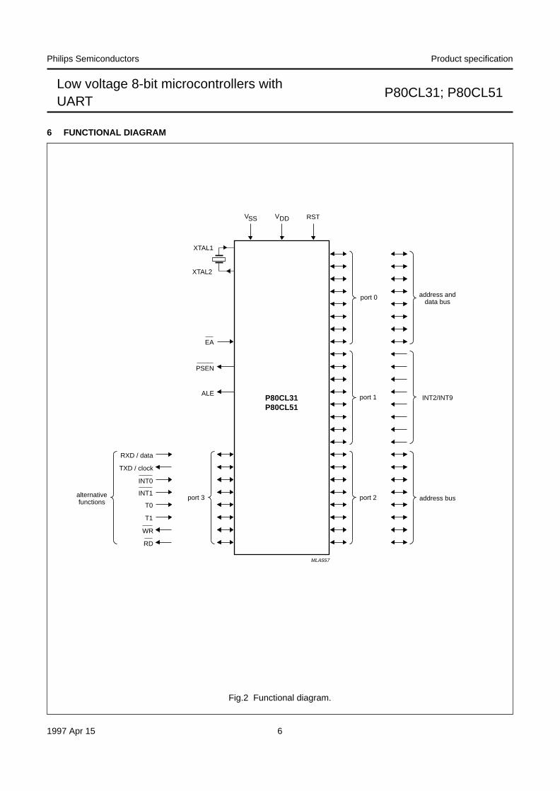
6 FUNCTIONAL DIAGRAM
Fig.2 Functional diagram.
handbook, full pagewidth
port 0 address and data bus
address bus
port 1
port 2
VDDVSS RST
XTAL1
XTAL2
ALE
EA
PSEN
port 3
RXD / data
TXD / clock
T0
T1
INT0
INT1
WR
RD
alternative functions
P80CL31 P80CL51
MLA557
INT2/INT9

1997 Apr 15 7
Philips Semiconductors Product specification
Low voltage 8-bit microcontrollers withUART
P80CL31; P80CL51
7 PINNING INFORMATION
7.1 Pinning
Fig.3 Pin configuration for DIP40 and VSO40 packages.
handbook, halfpage
MLA558
1
2
3
4
5
6
7
8
9
10
11
12
13
14
15
16
17
18
19
20
40
39
38
37
36
35
34
33
32
31
30
29
28
27
21
22
23
24
25
26
P0.4/AD4
P0.5/AD5
P0.6/AD6
P0.7/AD7
P2.7/A15
P2.6/A14
P2.5/A13
EA
PSEN
RST
P3.4/T0
P3.5/T1
P3.2/INT0
P3.3/INT1
ALE
P80CL31 P80CL51
XTAL2
XTAL1
P2.0/A8
P2.1/A9
P2.2/A10
P2.3/A11
P2.4/A12
V SS
P3.7/RD
P3.6/WR
V DD P1.0/INT2
P1.1/INT3
P1.2/INT4
P1.3/INT5
P1.4/INT6
P1.5/INT7
P1.6/INT8
P1.7/INT9
P3.0/RXD/data
P3.0/TXD/clock
P0.0/AD0
P0.1/AD1
P0.2/AD2
P0.3/AD3

1997 Apr 15 8
Philips Semiconductors Product specification
Low voltage 8-bit microcontrollers withUART
P80CL31; P80CL51
Fig.4 Pin configuration for QFP44 package.
handbook, full pagewidth
P80CL31 P83CL51
MBK034
1P1.5/INT7
2
3
4
5
6
7
8
9
10
11
33
32
31
30
29
28
27
26
25
24
23
12 13 14 15 16 17 18 19 20 21 22
44 43 42 41 40 39 38 37 36 35 34
P1.6/INT8
P1.7/INT9
RST
P3.0/RXD/data
n.c.
P3.1/TXD/clock
P3.2/INT0
P3.3/INT1
P3.4/T0
P3.5/T1
P3.
6/W
R
P3.
7/R
D
XT
AL2
XT
AL1 n.c.
P2.
0/A
8
P2.
1/A
9
P2.
2/A
10
P2.
3/A
11
P2.
4/A
12
P2.5/A13
P2.6/A14
P2.7/A15
PSEN
ALE
EA
n.c.
P0.7/AD7
P0.6/AD6
P0.5/AD5
P0.4/AD4
P0.
3/A
D3
P0.
2/A
D2
P0.
1/A
D1
P0.
0/A
D0
VD
D
n.c.
P1.
0/IN
T2
P1.
1/IN
T3
P1.
2/IN
T4
P1.
3/IN
T5
P1.
4/IN
T6
VS
S

1997 Apr 15 9
Philips Semiconductors Product specification
Low voltage 8-bit microcontrollers withUART
P80CL31; P80CL51
7.2 Pin description
Table 1 Pin description for DIP40 (SOT190-1), VSO40 (SOT319-2) and QFP44 (SOT307-2) packagesFor more extensive description of the port pins see Chapter 10 “I/O facilities”.
SYMBOL
PIN
DESCRIPTIONDIP40VSO40
QFP44
P1.0/INT2 1 40 · Port 1 : 8-bit bidirectional I/O port (P1.0 to P1.7). Port pins that havelogic 1s written to them are pulled HIGH by internal pull-ups, and in thisstate can be used as inputs. As inputs, Port 1 pins that are externallypulled LOW will source current (IIL, see Chapter 21) due to the internalpull-ups. Port 1 output buffers can sink/source 4 LS TTL loads.
· Alternative functions:
– INT2 to INT9 are external interrupt inputs.
P1.1/INT3 2 41
P1.2/INT4 3 42
P1.3/INT5 4 43
P1.4/INT6 5 44
P1.5/INT7 6 1
P1.6/INT8 7 2
P1.7/INT9 8 3
RST 9 4 Reset : a HIGH level on this pin for two machine cycles while the oscillatoris running resets the device.
P3.0/RXD/data 10 5 · Port 3: 8-bit bidirectional I/O port (P3.0 to P3.7).Same characteristics as Port 1.
· Alternative functions:
– RXD/data is the serial port receiver data input (asynchronous) or datainput/output (synchronous)
– TXD/clock is the serial port receiver data output (asynchronous) orclock output (synchronous)
– INT0 and INT1 are external interrupts 0 and 1
– T0 and T1 are external inputs for timers 0 and 1
– WR is the external Data Memory write strobe
– RD is the external Data Memory read strobe.
P3.1/TXD/clock 11 7
P3.2/INT0 12 8
P3.3/INT1 13 9
P3.4/T0 14 10
P3.5/T1 15 11
P3.6/WR 16 12
P3.7/RD 17 13
XTAL2 18 14 Crystal oscillator output : output of the inverting amplifier of the oscillator.Left open when external clock is used.
XTAL1 19 15 Crystal oscillator input : input to the inverting amplifier of the oscillator,also the input for an externally generated clock source.
VSS 20 16 Ground: circuit ground potential.
P2.0 to P2.7A8 to A15
21 to 28 18 to 25 · Port 2 : 8-bit bidirectional I/O port (P2.0 to P2.7) with internal pull-ups.Same characteristics as Port 1.
· High-order addressing : Port 2 emits the high-order address byte(A8 to A15) during accesses to external memory that use 16-bitaddresses (MOVX @DPTR). In this application it uses the strong internalpull-ups when emitting logic 1s. During accesses to external memory thatuse 8-bit addresses (MOVX @Ri), Port 2 emits the contents of the P2Special Function Register.
PSEN 29 26 Program Store Enable . Output read strobe to external Program Memory.When executing code out of external Program Memory, PSEN is activatedtwice each machine cycle. However, during each access to external DataMemory two PSEN activations are skipped.

1997 Apr 15 10
Philips Semiconductors Product specification
Low voltage 8-bit microcontrollers withUART
P80CL31; P80CL51
ALE 30 27 Address Latch Enable . Output pulse for latching the low byte of theaddress during access to external memory. ALE is emitted at a constantrate of 1 ¤ 6 ´ fosc, and may be used for external timing or clocking purposes(assuming MOVX instructions are not used).
EA 31 29 External Access . When EA is held HIGH the CPU executes out of internalprogram memory (unless the program counter exceeds 0FFFH). HoldingEA LOW forces the CPU to execute out of external memory regardless ofthe value of the program counter.
P0.7 to P0.0AD7 to AD0
32 to 39 30 to 37 · Port 0 : 8-bit open-drain bidirectional I/O port. As an open-drain outputport it can sink 8 LS TTL loads. Port 0 pins that have logic 1s written tothem float, and in that state will function as high impedance inputs.
· Low-order addressing : Port 0 is also the multiplexed low-order addressand data bus during access to external memory. The strong internalpull-ups are used while emitting logic 1s within the low order address.
VDD 40 38 Power supply.
n.c. - 6, 17, 28,39
Not connected.
SYMBOL
PIN
DESCRIPTIONDIP40VSO40
QFP44
1997 Apr 15 11
Philips Semiconductors Product specification
Low voltage 8-bit microcontrollers withUART
P80CL31; P80CL51
8 FUNCTIONAL DESCRIPTION OVERVIEW
This chapter gives a brief overview of the device.The detailed functional description is in the followingchapters as follows:
Chapter 9 “Memory organization”
Chapter 10 “I/O facilities”
Chapter 11 “Timers/event counters”
Chapter 12 “Reduced power modes”
Chapter 13 “Standard serial interface SIO0: UART”
Chapter 14 “Interrupt system”
Chapter 15 “Oscillator circuitry”
Chapter 16 “Reset”.
8.1 General
The P80CLx1 is a stand-alone high-performance CMOSmicrocontroller designed for use in real-time applicationssuch as instrumentation, industrial control, intelligentcomputer peripherals and consumer products.
The device provides hardware features, architecturalenhancements and new instructions to function as acontroller for applications requiring up to 64 kbytes ofProgram Memory and/or up to 64 kbytes of Data Memory.
The P80CLx1 contains 4 kbytes Program Memory (ROM;P80CL51 only); a static 128 bytes Data Memory (RAM);32 I/O lines; two16-bit timer/event counters;a thirteen-source, two priority-level, nested interruptstructure and on-chip oscillator and timing circuit.A standard UART serial interface is also provided.
The device has two software-selectable modes of reducedactivity for power reduction:
· Idle mode ; freezes the CPU while allowing the timers,serial I/O and interrupt system to continue functioning.
· Power-down mode ; saves the RAM contents butfreezes the oscillator causing all other chip functions tobe inoperative.
8.2 CPU timing
A machine cycle consists of a sequence of 6 states. Eachstate lasts for two oscillator periods, thus a machine cycletakes 12 oscillator periods or 1 m s if the oscillatorfrequency (fosc) is 12 MHz.

1997 Apr 15 12
Philips Semiconductors Product specification
Low voltage 8-bit microcontrollers withUART
P80CL31; P80CL51
9 MEMORY ORGANIZATION
The P80CLx1 has 4 kbytes of Program Memory (ROM;P80CL51 only) plus 128 bytes of Data Memory (RAM) onboard.The device has separate address spaces forProgram and Data Memory (see Fig.5). Using Port latchesP0 and P2, the P80CLx1 can address a maximum of64 kbytes of program memory and a maximum of64 kbytes of data memory. The CPU generates both read(RD) and write (WR) signals for external Data Memoryaccesses, and the read strobe (PSEN) for externalProgram Memory.
9.1 Program Memory
The P80CL51 contains 4 kbytes of internal ROM. Afterreset the CPU begins execution at location 0000H.The lower 4 kbytes of Program Memory can beimplemented in either on-chip ROM or external ProgramMemory.
If the EA pin is tied to VDD, then Program Memory fetchesfrom addresses 0000H to 0FFFH are directed to the
internal ROM. Fetches from addresses 1000H to FFFFHare directed to external ROM. Program Counter valuesgreater than 0FFFH are automatically addressed toexternal memory regardless of the state of the EA pin.
9.2 Data Memory
The P80CLx1 contains 128 bytes of internal RAM and 25Special Function Registers (SFR). The memory map(Fig.5) shows the internal Data Memory space divided intothe lower 128, the upper 128, and the SFR space.The lower 128 bytes of the internal RAM are organized asmapped in Fig.6. The lowest 32 bytes are grouped into 4banks of 8 registers. Program instructions refer to theseregisters within a register bank as R0 through R7. Two bitsin the Program Status Word select which register bank isin use. The next 16 bytes above the register banks form ablock of bit-addressable memory space. The 128 bits inthis area can be directly addressed by the single-bitmanipulation instructions. The remaining registers(30H to 7FH) are directly and indirectly byte addressable.
Fig.5 Memory map.
handbook, full pagewidth
MLA559
INTERNAL DATA RAM
255
127
0
EXTERNAL
(EA = 0)
INTERNAL
(EA = 1)
INTERNAL DATA MEMORY EXTERNAL DATA MEMORY
PROGRAM MEMORY
EXTERNAL 64K
64K
4096
4095 OVERLAPPED SPACE
0
4095
SPECIAL FUNCTION
REGISTERS

1997 Apr 15 13
Philips Semiconductors Product specification
Low voltage 8-bit microcontrollers withUART
P80CL31; P80CL51
Fig.6 The lower 128 bytes of internal RAM.
handbook, halfpage
MLA560 - 1
R7
R0
07H
0
R7
R0
0FH
08H
R7
R0
17H
10H
R7
R0
1FH
18H
2FH
7FH
20H
30H
bit-addressable space (bit addresses 0 to 7F)
4 banks of 8 registers (R0 to R7)
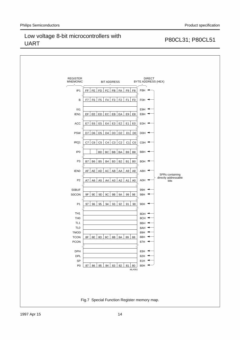
9.3 Special Function Registers (SFRs)
The upper 128 bytes are the address locations of theSFRs. Figure 7 shows the SFR space. The SFRs includethe port latches, timers, peripheral control, serial I/Oregisters, etc. These registers can only be accessed bydirect addressing. There are 128 directly addressablelocations in the SFR address space (SFRs with addressesdivisible by eight).
9.4 Addressing
The P8xCL410 has five methods for addressing sourceoperands:
· Register
· Direct
· Register-indirect
· Immediate
· Base-register plus index-register-indirect.
The first three methods can be used for addressingdestination operands. Most instructions have a‘destination/source’ field that specifies the data type,addressing methods and operands involved.For operations other than MOVs, the destination operandis also a source operand.
Access to memory addressing is as follows:
· Registers in one of the four register banks throughregister, direct or register-indirect
· Internal RAM (128 bytes) through direct orregister-indirect
· Special Function Registers through direct
· External data memory through register-indirect
· Program Memory look-up tables through base-registerplus index-register-indirect.
1997 Apr 15 14
Philips Semiconductors Product specification
Low voltage 8-bit microcontrollers withUART
P80CL31; P80CL51
Fig.7 Special Function Register memory map.
book, full pagewidth
MLA561
E6E7 E5 E4 E3 E2 E1 E0
D6D7 D5 D4 D3 D2 D1 D0
AEAF AD AC AB AA A9 A8
A6A7 A5 A4 A3 A2 A1 A0
9E9F 9D 9C 9B 9A 99 98
9697 95 94 93 92 91 90
8E8F 8D 8C 8B 8A 89 88
8687 85 84 83 82 81 80
BIT ADDRESSREGISTER MNEMONIC
DIRECT BYTE ADDRESS (HEX)
E0H
D0H
C0H
B8H
B0H
A8H
A0H
99H
98H
90H
8DH
8CH
8BH
8AH
89H
88H
87H
83H
82H
81H
80H
SFRs containing directly addressable
bits
ACC
PSW
P2
S0BUF
S0CON
P1
TH1
TH0
TL1
TL0
TMOD
PCON
DPH
DPL
SP
P0
IRQ1
IP0
P3
IEN0
TCON
EEEF ED EC EB EA E9 E8 E8HIEN1
E9H
F6F7 F5 F4 F3 F2 F1 F0 F0HB
FEFF FD FC FB FA F9 F8 F8HIP1
IX1
BD BC BB BA B9 B8
C6C7 C5 C4 C3 C2 C1 C0
B5 B4 B3 B2 B1 B0B6B7

1997 Apr 15 15
Philips Semiconductors Product specification
Low voltage 8-bit microcontrollers withUART
P80CL31; P80CL51
10 I/O FACILITIES
10.1 Ports
The P80CLx1 has 32 I/O lines treated as 32 individuallyaddressable bits or as four parallel 8-bit addressable ports.Ports 0, 1, 2 and 3 perform the alternative functionsdetailed below. To enable a port pin alternate function, theport bit latch in its SFR must contain a logic 1.
Port 0 Provides the multiplexed low-order address anddata bus for expanding the device with standardmemories and peripherals.
Port 1 Provides the inputs for the external interruptsINT2 to INT9.
Port 2 Provides the high-order address when expandingthe device with external Program or Data Memory.
Port 3 Pins can be configured individually to provide:
· External interrupt request inputs: INT1 and INT0
· Timer/counter inputs: T1 and T0
· Control signals to read and write to externalmemories: RD and WR
· UART input and output: RXD/data andTXD/clock.
Each port consists of a latch (SFRs P0 to P3), an outputdriver and input buffer. Ports 1, 2, and 3 have internalpull-ups Figure 8(a) shows that the strong transistor ‘p1’ isturned on for only 2 oscillator periods after a LOW-to-HIGHtransition in the port latch. When on, it turns on ‘p3’ (a weakpull-up) through the inverter. This inverter and ‘p3’ form alatch which holds the logic 1. In Port 0 the pull-up ‘p1’ isonly on when emitting logic 1s for external memoryaccess. Writing a logic 1 to a Port 0 bit latch leaves bothoutput transistors switched off so that the pin can be usedas a high-impedance input.
10.2 Port options
The pins of port 1, port 2 and port 3 may be individuallyconfigured with one of the following options. These optionsare also shown in Fig.8.
Option 1 Standard Port ; quasi-bidirectional I/O withpull-up. The strong booster pull-up ‘p1’ is turnedon for two oscillator periods after aLOW-to-HIGH transition in the port latch;Fig.8(a).
Option 2 Open-drain ; quasi-bidirectional I/O withn-channel open-drain output. Use as an outputrequires the connection of an external pull-upresistor; see Fig.8(b).
Option 3 Push-pull ; output with drive capability in bothpolarities. Under this option, pins can only beused as outputs; see Fig.8(c).
10.3 Port 0 options
The definition of port options for Port 0 is slightly different.Two cases are considered. First, access to externalmemory (EA = 0 or access above the built-in memoryboundary) and second, I/O accesses.
10.3.1 EXTERNAL MEMORY ACCESSES
Option 1 True logic 0 and logic 1 are written as address tothe external memory (strong pull-up to be used).
Option 2 An external pull-up resistor is required forexternal accesses.
Option 3 Not allowed for external memory accesses asthe port can only be used as output.
10.3.2 I/O ACCESSES
Option 1 When writing a logic 1 to the port latch, thestrong pull-up ‘p1’ will be on for 2 oscillatorperiods. No weak pull-up exists. Without anexternal pull-up, this option can be used as ahigh-impedance input.
Option 2 Open-drain; quasi-directional I/O with n-channelopen-drain output. Use as an output requires theconnection of an external pull-up resistor.See Fig.8(b).
Option 3 Push-Pull; output with drive capability in bothpolarities. Under this option pins can only beused as outputs. See Fig.8(c).
10.4 SET/RESET options
Individual mask selection of the post-reset state isavailable with any of the above pins. The requiredselection is made by appending ‘S’ or ‘R’ to Options 1, 2,or 3 above.
Option R RESET, at reset this pin will be initialized LOW.
Option S SET, at reset this pin will be initialized HIGH.

1997 Apr 15 16
Philips Semiconductors Product specification
Low voltage 8-bit microcontrollers withUART
P80CL31; P80CL51
Fig.8 Port configuration options.
handbook, full pagewidth
MGD677
p1
n
strong pull-up
+5 V
Q from port latch
(c) Push-pull
p1
p2
p3
input data
read port pin
2 oscillator periods
n
strong pull-up
I/O pin
+5 V
Q from port latch
INPUT BUFFER
(a) Standard
I/O pin
n
+5 V
Q from port latch
input data
read port pin
INPUT BUFFER
(b) Open-drain
external pull-up
I/O pin

1997 Apr 15 17
Philips Semiconductors Product specification
Low voltage 8-bit microcontrollers withUART
P80CL31; P80CL51
11 TIMERS/EVENT COUNTERS
The P80CLx1 contains two16-bit timer/event counterregisters; Timer 0 and Timer 1, which can perform thefollowing functions:
· Measure time intervals and pulse durations
· Count events
· Generate interrupt requests.
In the ‘Timer’ operating mode the register is incrementedevery machine cycle. Since a machine cycle consists of 12oscillator periods, the count rate is 1 ¤ 12 ´ fosc.
In the ‘Counter’ operating mode, the register isincremented in response to a HIGH-to-LOW transition.Since it takes 2 machine cycles (24 oscillator periods) torecognize a HIGH-to-LOW transition, the maximum countrate is 1 ¤ 24 ´ fosc. To ensure a given level is sampled, itshould be held for at least one complete machine cycle.
Timer 0 and Timer 1 can be programmed independently tooperate in four modes:
Mode 0 8-bit timer or 8-bit counter each with divide-by-32prescaler.
Mode 1 16-bit time-interval or event counter.
Mode 2 8-bit time-interval or event counter with automaticreload upon overflow.
Mode 3 Timer 0 establishes TL0 and TH0 as twoseparate counters.
12 REDUCED POWER MODES
There are two software selectable modes of reducedactivity for further power reduction: Idle and Power-down.
12.1 Idle mode
Idle mode operation permits the external interrupts, UART,and timer blocks to continue to function while the clock tothe CPU is halted.
Idle mode is entered by setting the IDL bit in the PowerControl Register (PCON.0, see Table 2). The instructionthat sets IDL is the last instruction executed in the normaloperating mode before the Idle mode is activated.
Once in Idle mode, the CPU status is preserved along withthe Stack Pointer, Program Counter, Program StatusWord and Accumulator. The RAM and all other registersmaintain their data during Idle mode. The status of theexternal pins during Idle mode is shown in Table 3.
The following functions remain active during the Idlemode:
· Timer 0 and Timer 1
· UART
· External interrupt.
These functions may generate an interrupt or reset; thusending the Idle mode.
There are two ways to terminate the Idle mode:
1. Activation of any enabled interrupt will cause IDL(PCON.0) to be cleared by hardware thus terminatingthe Idle mode. The interrupt is serviced, and followingthe RETI instruction, the next instruction to beexecuted will be the one following the instruction thatput the device in the Idle mode. The flag bits GF0(PCON.2) and GF1 (PCON.3) may be used todetermine whether the interrupt was received duringnormal execution or during the Idle mode.For example, the instruction that writes to PCON.0 canalso set or clear one or both flag bits. When the Idlemode is terminated by an interrupt, the service routinecan examine the status of the flag bits.
2. The second way of terminating the Idle mode is with anexternal hardware reset. Since the oscillator is stillrunning, the hardware reset is required to be active fortwo machine cycles (24 oscillator periods) to completethe reset operation. Reset redefines all SFRs but doesnot affect the on-chip RAM.
12.2 Power-down mode
Operation in Power-down mode freezes the oscillator.The internal connections which link both Idle andPower-down signals to the clock generation circuit areshown in Fig.9.
Power-down mode is entered by setting the PD bit in thePower Control Register (PCON.1, see Table 2).The instruction that sets PD is the last executed prior togoing into the Power-down mode.
Once in the Power-down mode, the oscillator is stopped.The contents of the on-chip RAM and the SFRs arepreserved. The port pins output the value held by theirrespective SFRs. ALE and PSEN are held LOW.
In the Power-down mode, VDD may be reduced tominimize circuit power consumption. The supply voltagemust not be reduced until the Power-down mode isentered, and must be restored before the hardware resetis applied which will free the oscillator. Reset should not bereleased until the oscillator has restarted and stabilized.

1997 Apr 15 18
Philips Semiconductors Product specification
Low voltage 8-bit microcontrollers withUART
P80CL31; P80CL51
12.3 Wake-up from Power-down mode
When in Power-down mode the controller can bewoken-up with either the external interrupts INT2 to INT9,or a reset operation. The wake-up operation has two basicapproaches as explained in Section 12.3.1; 12.3.2 andillustrated in Fig.10.
12.3.1 WAKE-UP USING INT2 TO INT9
If any of the interrupts INT2 to INT9 are enabled, thedevice can be woken-up from the Power-down mode withthe external interrupts. To ensure that the oscillator isstable before the controller restarts, the internal clock willremain inactive for 1536 oscillator periods. This iscontrolled by an on-chip delay counter.
12.3.2 WAKE-UP USING RST
To wake-up the P80CLx1, the RST pin must be kept HIGHfor a minimum of 24 periods. The on-chip delay counter isinactive. The user must ensure that the oscillator is stablebefore any operation is attempted.
12.4 Power Control Register (PCON)
See Tables 2 and 3. Idle and Power-down modes areactivated by software using this SFR. PCON is notbit-addressable.
12.5 Status of external pins
The status of the external pins during Idle and Power-downmode is shown in Table 4. If the Power-down mode isactivated whilst accessing external Program Memory, theport data that is held in the Special Function Register P2 isrestored to Port 2.
If the data is a logic 1, the port pin is held HIGH during thePower-down mode by the strong pull-up transistor ‘p1’;see Fig.8(a).
Table 2 Power Control Register (address 87H)
Table 3 Description of PCON bits
Table 4 Status of external pins during Idle and Power-down modes
7 6 5 4 3 2 1 0
SMOD - - - GF1 GF0 PD IDL
BIT SYMBOL DESCRIPTION
7 SMOD Double Baud rate bit; see description of UART
6, 5, 4 - reserved
3 and 2 GF1 and GF0 General purpose flag bits
1 PD Power-down bit; setting this bit activates the Power-down mode
0 IDL Idle mode bit; setting this bit activates the Idle mode
MODE MEMORY ALE PSEN PORT 0 PORT 1 PORT 2 PORT 3 PORT 4
Idle internal 1 1 port data port data port data port data port data
external 1 1 floating port data address port data port data
Power-down internal 0 0 port data port data port data port data port data
external 0 0 floating port data port data port data port data

1997 Apr 15 19
Philips Semiconductors Product specification
Low voltage 8-bit microcontrollers withUART
P80CL31; P80CL51
Fig.9 Internal clock control in Idle and Power-down mode.
handbook, full pagewidth
MLA563
OSCILLATOR
CLOCK GENERATOR
interrupts serial ports timer blocks
CPU
IDLPD
XTAL1XTAL2
Fig.10 Wake-up operation.
handbook, full pagewidth
MGD679
delay counter 1536 periods
24 periods
power-down
RST pin
external interrupt
oscillator

1997 Apr 15 20
Philips Semiconductors Product specification
Low voltage 8-bit microcontrollers withUART
P80CL31; P80CL51
13 STANDARD SERIAL INTERFACE SIO0: UART
This serial port is full duplex which means that it cantransmit and receive simultaneously. It is alsoreceive-buffered and can commence reception of asecond byte before a previously received byte has beenread from the register. (However, if the first byte has notbeen read by the time the reception of the second byte iscomplete, one of the bytes will be lost). The serial portreceive and transmit registers are both accessed via theSpecial Function Register S0BUF. Writing to S0BUF loadsthe transmit register and reading S0BUF accesses aphysically separate receive register.
The serial port can operate in 4 modes:
Mode 0 Serial data enters and exits through RXD. TXDoutputs the shift clock. Eight bits aretransmitted/received (LSB first). The baud rate isfixed at 1 ¤ 12 ´ fosc.
Mode 1 10 bits are transmitted (through TXD) or received(through RXD): a start bit (logic 0), 8 data bits(LSB first), and a stop bit (logic 1). On receive,the stop bit goes into RB8 in Special FunctionRegister S0CON. The baud rate is variable.
Mode 2 11 bits are transmitted (through TXD) or received(through RXD): start bit (logic 0), 8 data bits (LSBfirst), a programmable 9th data bit, and a stop bit(logic 1). On transmit, the 9th data bit (TB8 inS0CON) can be assigned the value of a logic 0 orlogic 1. Or, for example, the parity bit (P, in thePSW) could be moved into TB8. On receive, the9th data bit goes into RB8 in S0CON, while thestop bit is ignored. The baud rate isprogrammable to either 1 ¤ 32 or 1¤ 64 ´ fosc.
Mode 3 11 bits are transmitted (through TXD) or received(through RXD): a start bit (logic 0), 8 data bits(LSB first), a programmable 9th data bit and astop bit (logic 1). In fact, Mode 3 is the same asMode 2 in all respects except baud rate.The baud rate in Mode 3 is variable.
In all four modes, transmission is initiated by anyinstruction that uses S0BUF as a destination register.Reception is initiated in Mode 0 by the condition RI = 0 andREN = 1. Reception is initiated in the other modes by theincoming start bit if REN = 1.
13.1 Multiprocessor communications
Modes 2 and 3 have a special provision for multiprocessorcommunications. In these modes, 9 data bits are received.The 9th bit goes into RB8. The following bit is the stop bit.The port can be programmed such that when the stop bitis received, the serial port interrupt will be activated, butonly if RB8 = 1. This feature is enabled by setting bit SM2in S0CON. One use of this feature, in multiprocessorsystems, is as follows.
When the master processor wants to transmit a block ofdata to one of several slaves, it first sends out an addressbyte which identifies the target slave. An address bytediffers from a data byte in that the 9th bit is HIGH in anaddress byte and LOW in a data byte. With SM2 = 1,no slave will be interrupted by a data byte. An addressbyte, however, will interrupt all slaves, so that each slavecan examine the received byte and see if it is beingaddressed. The addressed slave will clear its SM2 bit andprepare to receive the data bytes that will be sent. Theslaves that were not being addressed leave their SM2 bitsset and go on about their business, ignoring the comingdata bytes.
SM2 has no effect in Mode 0, and in Mode 1 can be usedto check the validity of the stop bit. In a Mode 1 reception,if SM2 = 1, the receive interrupt will not be activated unlessa valid stop bit is received.
13.2 Serial Port Control and Status Register(S0CON)
The Serial Port Control and Status Register is the SpecialFunction Register S0CON. The register contains not onlythe mode selection bits, but also the 9th data bit for transmitand receive (TB8 and RB8), and the serial port interruptbits (TI and RI).

1997 Apr 15 21
Philips Semiconductors Product specification
Low voltage 8-bit microcontrollers withUART
P80CL31; P80CL51
Table 5 Serial Port Control Register (address 98H)
Table 6 Description of S0CON bits
Table 7 Selection of the serial port modes
7 6 5 4 3 2 1 0
SM0 SM1 SM2 REN TB8 RB8 TI RI
BIT SYMBOL DESCRIPTION
7 SM0 These bits are used to select the serial port mode; see Table 7.
6 SM1
5 SM2 Enables the multiprocessor communication feature in Modes 2 and 3. In these modes, ifSM2 = 1, then RI will not be activated if the received 9th data bit (RB8) is a logic 0.In Mode 1, if SM2 = 1, then RI will not be activated unless a valid stop bit was received.In Mode 0, SM2 should be a logic 0.
4 REN Enables serial reception and is set by software to enable reception, and cleared bysoftware to disable reception.
3 TB8 Is the 9th data bit that will be transmitted in Modes 2 and 3; set or cleared by software asdesired.
2 RB8 In Modes 2 and 3, is the 9th data bit received. In Mode 1, if SM2 = 0 then RB8 is the stopbit that was received; in Mode 0, RB8 is not used.
1 TI The transmit interrupt flag . Set by hardware at the end of the 8th bit time in Mode 0, orat the beginning of the stop bit time in the other modes, in any serial transmission. Mustbe cleared by software.
0 RI The receive interrupt flag . Set by hardware at the end of the 8th bit time in Mode 0, orhalfway through the stop bit time in the other modes, in any serial transmission (exceptsee SM2). Must be cleared by software.
SM0 SM1 MODE DESCRIPTION BAUD RATE
0 0 Mode 0 Shift register 1¤ 12 ´ fosc
0 1 Mode 1 8-bit UART variable
1 0 Mode 2 9-bit UART 1¤ 32 or 1 ¤ 64 ´ fosc
1 1 Mode 3 9-bit UART variable

1997 Apr 15 22
Philips Semiconductors Product specification
Low voltage 8-bit microcontrollers withUART
P80CL31; P80CL51
13.3 Baud rates
The baud rate in Mode 0 is fixed and may be calculated as:
The baud rate in Mode 2 depends on the value of theSMOD bit in Special Function Register PCON and may becalculated as:
· If SMOD = 0 (value on reset), the baud rate is 1 ¤ 64 ´ fosc
· If SMOD = 1, the baud rate is 1 ¤ 32 ´ fosc
The baud rates in Modes 1 and 3 are determined by theTimer 1 or Timer 2 overflow rate.
13.3.1 USING TIMER 1 TO GENERATE BAUD RATES
When Timer 1 is used as the Baud Rate Generator, thebaud rates in Modes 1 and 3 are determined by theTimer 1 overflow rate and the value of the SMOD bit as
Baud Ratefosc
12--------=
Baud Rate2
SMOD
64----------------- fosc´=
follows:
The Timer 1 interrupt should be disabled in thisapplication. The Timer itself can be configured for either‘timer’ or ‘counter’ operation in any of its 3 running modes.In most typical applications, it is configured for ‘timer’operation, in the Auto-reload mode (high nibble ofTMOD = 0010B). In this case the baud rate is given by theformula:
By configuring Timer 1 to run as a 16-bit timer (high nibbleof TMOD = 0001B), and using the Timer 1 interrupt to doa 16-bit software reload, very low baud rates can beachieved. Table 8 lists commonly used baud rates andhow they can be obtained from Timer 1.
Baud Rate 2SMOD
32----------------- Timer 1 Overflow Rate.´=
Baud Rate2
SMOD
32-----------------
fosc
12 256 TH1–( )´{ }--------------------------------------------------------´=
Table 8 Commonly used baud rates generated by Timer 1
Notes
1. Maximum in Mode 0.
2. X = don’t care.
3. Maximum in Mode 2.
4. Maximum in Modes 1 and 3.
BAUD RATE (kbits/s) f osc (MHz) SMOD C/T TIMER 1 MODE RELOAD VALUE
1330.0(1) 16.000 X(2) X X X
500.0(3) 16.000 1 X X X
83.3(4) 16.000 1 0 Mode 2 FFH
19.2 11.059 1 0 Mode 2 FDH
9.6 11.059 0 0 Mode 2 FDH
4.8 11.059 0 0 Mode 2 FAH
2.4 11.059 0 0 Mode 2 F4H
1.2 11.059 0 0 Mode 2 E8H
137.5 11.986 0 0 Mode 2 1DH
110.0 6.000 0 0 Mode 2 72H
110.0 12.000 0 0 Mode 1 FEEBH

1997 Apr 15 23
Philips Semiconductors Product specification
Low voltage 8-bit microcontrollers withUART
P80CL31; P80CL51
Fig.11 Serial port Mode 0.
andbook, full pagewidth
MGC752
START SHIFT
T1
TX CONTROLTX CLOCK SEND
serial port interrupt
RX CLOCKR1
SHIFTRX CONTROL
START
INPUT SHIFT REGISTER
S0 BUFFER
INTERNAL BUS
READ SBUF
SHIFTLOAD SBUF
S0 BUFFER
ZERO DETECTORSHIFT
D
CL
SQ
INTERNAL BUS
write to SBUF
1 1 1 1 1 1 1 0
REN
S6
RI
RXD P3.0 ALT
output function
RECEIVE
SHIFT CLOCK
TXD P3.1 ALT
output function
RXD P3.0 ALT
input function

1997 Apr 15 24
Philips Semiconductors Product specification
Low voltage 8-bit microcontrollers withUART
P80CL31; P80CL51
handbook, full pagewidth
MLA
567
s1...
s6s1
...s6
s1...
s6s1
...s6
s1...
s6s1
...s6
s1...
s6s1
...s6
s1...
s6s1
...s6
s1...
s6s1
...s6
s1...
s6s1
...s6
s1...
s6s1
...s6
s1...
s6s1
...s6
s1...
s6s1
...s6
...s6
WR
ITE
TO
SB
UF
S6P
2
D0
D1
D2
D3
D4
D5
D6
D7
S3P
1S
6P1
WR
ITE
TO
SC
ON
(C
LEA
R R
1)
D0
D1
D2
D3
D4
D5
D6
D7
S5P
2
ALE
SE
ND
SH
IFT
RX
D (
DA
TA
OU
T)
TS
C (
SH
IFT
CLO
CK
)
RI
RE
CE
IVE
SH
IFT
RX
D (
DA
TA
IN)
TX
D (
SH
IFT
CLO
CK
)
T
R
A
N
S
M I T R
E
C
E I V
E
Fig
.12
Ser
ial p
ort M
ode
0 tim
ing.

1997 Apr 15 25
Philips Semiconductors Product specification
Low voltage 8-bit microcontrollers withUART
P80CL31; P80CL51
dbook, full pagewidth
MGC755
STARTSHIFT
DATA
T1
TX CONTROLTX CLOCK SEND16
serial port interrupt
16
RX CLOCK R1 LOAD SBUF
SHIFTRX CONTROLSTART
sample
INPUT SHIFT REGISTER
(9-BITS)
BIT DETECTOR
S0 BUFFER
INTERNAL BUS
READ SBUF
SHIFT
LOAD SBUF
S0 BUFFER
ZERO DETECTORSHIFT
D
CL
SQ
TB8
INTERNAL BUS
write to SBUF
RXD
TXD
0
SMOD
RTCLK
1
0 1
HIGH-TO-LOW TRANSITION DETECTOR
2
Timer 1 overflow
Timer 2 overflow
Fig.13 Serial port Mode 1.

1997 Apr 15 26
Philips Semiconductors Product specification
Low voltage 8-bit microcontrollers withUART
P80CL31; P80CL51
Fig
.14
Ser
ial p
ort M
ode
1 tim
ing.
handbook, full pagewidth
MLA
569
D0
D1
D2
D3
D4
D5
D6
D7
ST
AR
T B
IT
D0
D1
D2
D3
D4
D5
D6
D7
TX
CLO
CK
WR
ITE
TO
SB
UF
DA
TA
SH
IFT
TX
D
TI
ST
AR
T B
IT
S1P
1
ST
OP
BIT
÷16
RE
SE
T
RX
CLO
CK
RX
D
ST
OP
BIT
BIT
DE
TE
CT
OR
SA
MP
LE T
IME
SH
IFT
RI
SE
ND
T
R
A
N
S
M I T
R
E
C
E I V
E

1997 Apr 15 27
Philips Semiconductors Product specification
Low voltage 8-bit microcontrollers withUART
P80CL31; P80CL51
Fig.15 Serial port Mode 2.
handbook, full pagewidth
MGC754
STARTSTOP BIT SHIFT
DATA
T1
TX CONTROLTX CLOCK SEND16
serial port interrupt
16
RX CLOCK R1 LOAD SBUF
SHIFTRX CONTROLSTART
sample
INPUT SHIFT REGISTER
(9-BITS)
BIT DETECTOR
S0 BUFFER
INTERNAL BUS
READ SBUF
SHIFT
LOAD SBUF
S0 BUFFER
ZERO DETECTORSHIFT
D
CL
SQ
TB8
INTERNAL BUS
write to SBUF
2
phase 2 clock (fosc / 2)
RXD
TXD
0CSMOD at
PCON.7
1
HIGH-TO-LOW TRANSITION DETECTOR

1997 Apr 15 28
Philips Semiconductors Product specification
Low voltage 8-bit microcontrollers withUART
P80CL31; P80CL51
handbook, full pagewidth
TX
CLO
CK
ST
OP
BIT
GE
N
RX
CLO
CK
BIT
DE
TE
CT
OR
SA
MP
LE T
IME
SH
IFT
MLA
571
D0
D1
D2
D3
D4
D5
D6
D7
TB
8
WR
ITE
TO
SB
UF
SE
ND
DA
TA
SH
IFT
TX
D
TI
ST
AR
T B
IT
S1P
1
ST
OP
BIT
÷16
RE
SE
T
ST
AR
T B
IT
RX
DD
0D
1D
2D
3D
4D
5D
6D
7S
TO
P B
IT
RI
RB
8
T
R
A
N
S
M I T
R
E
C
E I V
E
Fig
.16
Ser
ial p
ort M
ode
2 tim
ing.

1997 Apr 15 29
Philips Semiconductors Product specification
Low voltage 8-bit microcontrollers withUART
P80CL31; P80CL51
Fig.17 Serial port Mode 3.
handbook, full pagewidth
MGC753
STARTSHIFT
DATA
T1
0
SMOD
RTCLK
1
0 1
TX CONTROLTX CLOCK SEND16
serial port interrupt
16
RX CLOCK R1 LOAD SBUF
SHIFTRX CONTROLSTART
HIGH-TO-LOW TRANSITION DETECTOR
sample
INPUT SHIFT REGISTER
(9-BITS)
BIT DETECTOR
S0 BUFFER
INTERNAL BUS
READ SBUF
SHIFT
LOAD SBUF
S0 BUFFER
ZERO DETECTORSHIFT
D
CL
SQ
TB8
INTERNAL BUS
write to SBUF
2
Timer 1 overflow
Timer 2 overflow
RXD
TXD
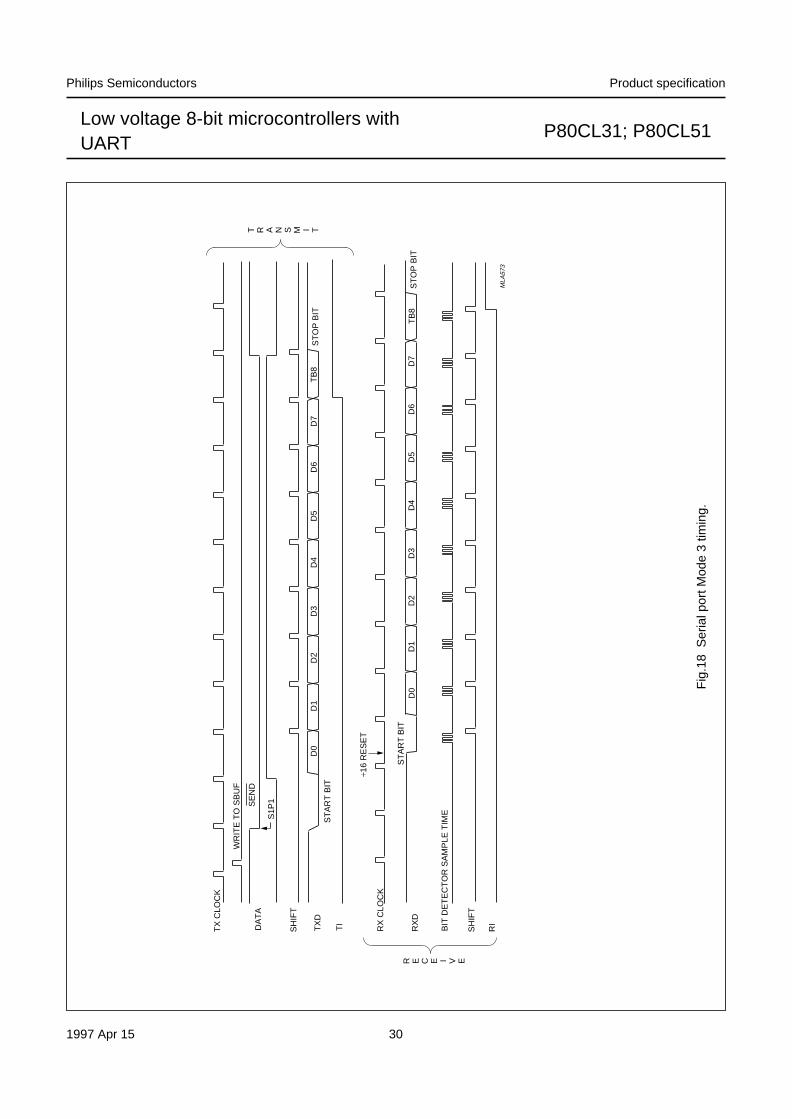
1997 Apr 15 30
Philips Semiconductors Product specification
Low voltage 8-bit microcontrollers withUART
P80CL31; P80CL51
Fig
.18
Ser
ial p
ort M
ode
3 tim
ing.
handbook, full pagewidth
MLA
573
D0
D1
D2
D3
D4
D5
D6
D7
TX
CLO
CK
WR
ITE
TO
SB
UF
SE
ND
DA
TA
SH
IFT
TX
D
TI
ST
AR
T B
IT
S1P
1
ST
OP
BIT
÷16
RE
SE
T
ST
AR
T B
IT
RX
CLO
CK
RX
DD
0D
1D
2D
3D
4D
5D
6D
7S
TO
P B
IT
BIT
DE
TE
CT
OR
SA
MP
LE T
IME
SH
IFT
RI
TB
8
TB
8
T
R
A
N
S
M I T
R
E
C
E I V
E

1997 Apr 15 31
Philips Semiconductors Product specification
Low voltage 8-bit microcontrollers withUART
P80CL31; P80CL51
14 INTERRUPT SYSTEM
External events and the real-time-driven on-chipperipherals require service by the CPU at unpredictabletimes. To tie the asynchronous activities of these functionsto normal program execution a multiple-source,two-priority-level, nested interrupt system is provided.The system is shown in Fig.19. The P80CLx1acknowledges interrupt requests from thirteen sources asfollows:
· INT0 to INT9
· Timer 0 and Timer 1
· UART.
Each interrupt vectors to a separate location in ProgramMemory for its service routine. Each source can beindividually enabled or disabled by corresponding bits inthe Interrupt Enable Registers (IEN0 and IEN1).The priority level is selected via the Interrupt PriorityRegisters (IP0 and IP1). All enabled sources can beglobally disabled or enabled. Figure 19 shows the interruptsystem.
14.1 External interrupts INT2 to INT9
Port 1 lines serve an alternative purpose as eightadditional interrupts INT2 to INT9. When enabled, each ofthese lines may wake-up the device from the Power-downmode. Using the Interrupt Polarity Register (IX1), each pinmay be initialized to be either active HIGH or active LOW.IRQ1 is the Interrupt Request Flag Register. If the interruptis enabled, each flag will be set on an interrupt request butmust be cleared by software, i.e. via the interrupt softwareor when the interrupt is disabled.
Port 1 interrupts are level sensitive. A Port 1 interrupt willbe recognized when a level (HIGH or LOW depending onthe Interrupt Polarity Register) on P1.n is held active for atleast one machine cycle. The interrupt request is notserviced until the next machine cycle. Figure 20 shows theexternal interrupt configuration.
14.2 Interrupt priority
Each interrupt source can be set to either a high priority orto a low priority. If a low priority interrupt is receivedsimultaneously with a high priority interrupt, the highpriority interrupt will be dealt with first.
If interrupts of the same priority are requestedsimultaneously, the processor will branch to the interruptpolled first, according to the sequence shown in Table 9and in Fig.19. The ‘vector address’ is the ROM locationwhere the appropriate interrupt service routine starts.
Table 9 Interrupt vector polling sequence
A low priority interrupt routine can only be interrupted by ahigh priority interrupt. A high priority interrupt routinecannot be interrupted.
SYMBOLVECTOR
ADDRESS (HEX)SOURCE
X0 (first) 0003 External 0
S0 002B UART
X5 0053 External 5
T0 000B Timer 0
X6 005B External 6
X1 0013 External 1
X2 003B External 2
X7 0063 External 7
T1 001B Timer 1
X3 0043 External 3
X8 006B External 8
X4 004B External 4
X9 (last) 0073 External 9

1997 Apr 15 32
Philips Semiconductors Product specification
Low voltage 8-bit microcontrollers withUART
P80CL31; P80CL51
Fig.19 Interrupt system.
handbook, full pagewidth INTERRUPT SOURCES REGISTERS
PRIORITY
GLOBAL ENABLE
X0
S0
X5
T0
X6
X1
X2
X7
T1
X3
X8
X4
X9
IEN0/1 IP0/1
HIGH
LOW
INT
ER
RU
PT
PO
LLIN
G S
EQ
UE
NC
E
MLA574

1997 Apr 15 33
Philips Semiconductors Product specification
Low voltage 8-bit microcontrollers withUART
P80CL31; P80CL51
14.3 Interrupt registers
The registers used in the interrupt system are listed in Table 10. Tables 11 to 22 describe the contents of these registers.
Table 10 Special Function Registers related to the interrupt system
ADDRESS REGISTER DESCRIPTION
A8H IEN0 Interrupt Enable Register
E8H IEN1 Interrupt Enable Register (INT2 to INT9)
B8H IP0 Interrupt Priority Register
F8H IP1 Interrupt Priority Register (INT2 to INT9
E9H IX1 Interrupt Polarity Register
C0H IRQ1 Interrupt Request Flag Register
Fig.20 External interrupt configuration.
handbook, full pagewidth
MLA575
P1.7
P1.6
P1.5
P1.4
P1.3
P1.2
P1.1
P1.0
X9
X8
X7
X6
X5
X4
X3
X2
IX1 IEN1 IRQ1
WAKE-UP

1997 Apr 15 34
Philips Semiconductors Product specification
Low voltage 8-bit microcontrollers withUART
P80CL31; P80CL51
14.3.1 INTERRUPT ENABLE REGISTER (IEN0)
Bit values: 0 = interrupt disabled; 1 = interrupt enabled.
Table 11 Interrupt Enable Register (SFR address A8H)
Table 12 Description of IEN0 bits
14.3.2 INTERRUPT ENABLE REGISTER (IEN1)
Bit values: 0 = interrupt disabled; 1 = interrupt enabled.
Table 13 Interrupt Enable Register (SFR address E8H)
Table 14 Description of IEN1 bits
7 6 5 4 3 2 1 0
EA - - ES0 ET1 EX1 ET0 EX0
BIT SYMBOL DESCRIPTION
7 EA general enable/disable control. If EA = 0, no interrupt is enabled; if EA = 1, anyindividually enabled interrupt will be accepted
6 - reserved
5 - reserved
4 ES0 enable UART SIO interrupt
3 ET1 enable Timer 1 interrupt (T1)
2 EX1 enable external interrupt 1
1 ET0 enable Timer 0 interrupt (T0)
0 EX0 enable external interrupt 0
7 6 5 4 3 2 1 0
EX9 EX8 EX7 EX6 EX5 EX4 EX3 EX2
BIT SYMBOL DESCRIPTION
7 EX9 enable external interrupt 9
6 EX8 enable external interrupt 8
5 EX7 enable external interrupt 7
4 EX6 enable external interrupt 6
3 EX5 enable external interrupt 5
2 EX4 enable external interrupt 4
1 EX3 enable external interrupt 3
0 EX2 enable external interrupt 2

1997 Apr 15 35
Philips Semiconductors Product specification
Low voltage 8-bit microcontrollers withUART
P80CL31; P80CL51
14.3.3 INTERRUPT PRIORITY REGISTER (IP0)
Bit values: 0 = low priority; 1 = high priority.
Table 15 Interrupt Priority Register (SFR address B8H)
Table 16 Description of IP0 bits
14.3.4 INTERRUPT PRIORITY REGISTER (IP1)
Bit values: 0 = low priority; 1 = high priority.
Table 17 Interrupt Priority Register (SFR address F8H)
Table 18 Description of IP1 bits
7 6 5 4 3 2 1 0
- - - PS0 PT1 PX1 PT0 PX0
BIT SYMBOL DESCRIPTION
7 - reserved
6 - reserved
5 - reserved
4 PS0 UART SIO interrupt priority level
3 PT1 Timer 1 interrupt priority level
2 PX1 external interrupt 1 priority level
1 PT0 Timer 0 interrupt priority level
0 PX0 external interrupt 0 priority level
7 6 5 4 3 2 1 0
PX9 PX8 PX7 PX6 PX5 PX4 PX3 PX2
BIT SYMBOL DESCRIPTION
7 PX9 external interrupt 9 priority level
6 PX8 external interrupt 8 priority level
5 PX7 external interrupt 7 priority level
4 PX6 external interrupt 6 priority level
3 PX5 external interrupt 5 priority level

1997 Apr 15 36
Philips Semiconductors Product specification
Low voltage 8-bit microcontrollers withUART
P80CL31; P80CL51
14.3.5 INTERRUPT POLARITY REGISTER (IX1)
Writing either a logic 1 or logic 0 to any Interrupt Polarity Register bit sets the polarity level of the corresponding externalinterrupt to an active HIGH or active LOW respectively.
Table 19 Interrupt Polarity Register (SFR address E9H)
Table 20 Description of IX1 bits
14.3.6 INTERRUPT REQUEST FLAG REGISTER (IRQ1)
Table 21 Interrupt Request Flag Register (SFR address C0H)
Table 22 Description of IRQ1 bits
2 PX4 external interrupt 4 priority level
1 PX3 external interrupt 3 priority level
0 PX2 external interrupt 2 priority level
7 6 5 4 3 2 1 0
IL9 IL8 IL7 IL6 IL5 IL4 IL3 IL2
BIT SYMBOL DESCRIPTION
7 IL9 external interrupt 9 polarity level
6 IL8 external interrupt 8 polarity level
5 IL7 external interrupt 7 polarity level
4 IL6 external interrupt 6 polarity level
3 IL5 external interrupt 5 polarity level
2 IL4 external interrupt 4 polarity level
1 IL3 external interrupt 3 polarity level
0 IL2 external interrupt 2 polarity level
7 6 5 4 3 2 1 0
IQ9 IQ8 IQ7 IQ6 IQ5 IQ4 IQ3 IQ2
BIT SYMBOL DESCRIPTION
7 IQ9 external interrupt 9 request flag
6 IQ8 external interrupt 8 request flag
5 IQ7 external interrupt 7 request flag
4 IQ6 external interrupt 6 request flag
3 IQ5 external interrupt 5 request flag
2 IQ4 external interrupt 4 request flag
1 IQ3 external interrupt 3 request flag
0 IQ2 external interrupt 2 request flag
BIT SYMBOL DESCRIPTION

1997 Apr 15 37
Philips Semiconductors Product specification
Low voltage 8-bit microcontrollers withUART
P80CL31; P80CL51
15 OSCILLATOR CIRCUITRY
The on-chip oscillator circuitry of the P80CLx1 is asingle-stage inverting amplifier biased by an internalfeedback resistor. The oscillator circuit is shown in Fig.22.For operation as a standard quartz oscillator, no externalcomponents are needed, except for the 32 kHz option.When using external capacitors, ceramic resonators, coilsand RC networks to drive the oscillator, five differentconfigurations are supported (see Table 23 and Fig.21).
In the Power-down mode the oscillator is stopped andXTAL1 is pulled HIGH. The oscillator inverter is switchedoff to ensure no current will flow regardless of the voltageat XTAL1, for configurations (a), (b), (c), (d), (e) and (g) ofFig.21.
To drive the device with an external clock source, apply theexternal clock signal to XTAL1, and leave XTAL2 to float,as shown in Fig.21(f). There are no requirements on theduty cycle of the external clock, since the input to theinternal clocking circuitry is buffered by a flip-flop.
Various oscillator options are provided for optimumon-chip oscillator performance; these are specified inTable 23 and shown in Fig.21. The required option shouldbe stated when ordering.
Table 23 Oscillator options
OPTION APPLICATION
Oscillator 1 for 32 kHz clock applications with external trimmer for frequency adjustment; a 4.7 MW bias resistoris needed for use in parallel with the crystal; see Fig.21(c)
Oscillator 2 low-power, low-frequency operations using LC components; see Fig.21(e)
Oscillator 3 medium frequency range applications
Oscillator 4 high frequency range applications
RC oscillator RC oscillator configuration; see Figs 21(g) and 23
handbook, full pagewidth
MLA577
VDD
XTAL1 XTAL2
(d)
XTAL1 XTAL2
(e)
XTAL1 XTAL2
(f)
XTAL1 XTAL2
(g)
n.c. n.c.
XTAL1 XTAL2
(b)
XTAL1 XTAL2
(c)
XTAL1 XTAL2
(a)
STANDARD QUARTZ
OSCILLATOR
QUARTZ OSCILLATOR WITH EXTERNAL
CAPACITORS32 kHz
OSCILLATOR
CERAMIC RESONATOR LC - OSCILLATOR EXTERNAL CLOCK RC - OSCILLATOR
Fig.21 Oscillator configurations.

1997 Apr 15 38
Philips Semiconductors Product specification
Low voltage 8-bit microcontrollers withUART
P80CL31; P80CL51
Fig.22 Standard oscillator.
handbook, full pagewidth
MLA576
VDD
P80CL31 P80CL51
VDD
RbiasC1i C2i
XTAL1 XTAL2
to internal timing circuits
VDD
PD
Fig.23 RC oscillator frequency as a function of RC.
handbook, halfpage
0
600
400
200
02 4 6
MLA579
RC ( m s)
(kHz)
fosc
RC oscillator frequency is externally adjustable; 100 kHz £ fosc £ 500 kHz.

1997 Apr 15 39
Philips Semiconductors Product specification
Low voltage 8-bit microcontrollers withUART
P80CL31; P80CL51
Table 24 Oscillator type selection guide
Note
1. 32 kHz quartz crystals with a series resistance >15 kW will reduce the guaranteed supply voltage range to2.5 to 3.5 V.
RESONATORFREQUENCY
(MHz)OPTION
(see Table 23)
C1 EXT. (pF) C2 EXT. (pF) RESONATOR MAX.SERIES RESISTANCEMIN. MAX. MIN. MAX.
Quartz 0.032 Oscillator 1 0 0 5 15 15 kW (1)
1.0
Oscillator 2
0 30 0 30 600 W3.58 0 15 0 15 100 W4.0 0 20 0 20 75 W6.0 Oscillator 3 0 10 0 10 60 W
10.0
Oscillator 4
0 15 0 15 60 W12.0 0 10 0 10 40W16.0 0 15 0 15 20 W
PXE 0.455
Oscillator 2
40 50 40 50 10 W1.0 15 50 15 50 100 W3.58 0 40 0 40 10 W4.0 0 40 0 40 10 W6.0 0 20 0 20 5 W
10.0 Oscillator 3 0 15 0 15 6 W12.0 Oscillator 4 10 40 10 40 6 W
LC - Oscillator 2 20 90 20 90 10 m H = 1 W
100 m H = 5 W
1 mH = 75 W

1997 Apr 15 40
Philips Semiconductors Product specification
Low voltage 8-bit microcontrollers withUART
P80CL31; P80CL51
Table 25 Oscillator equivalent circuit parametersThe equivalent circuit data of the internal oscillator compares with that of matched crystals.
SYMBOL PARAMETER OPTION CONDITION MIN. TYP. MAX. UNIT
gm transconductance Oscillator 1; 32 kHz Tamb = +25 °C;VDD = 4.5 V
- 15 - m S
Oscillator 2 200 600 1000 m S
Oscillator 3 400 1500 4000 m S
Oscillator 4 1000 4000 10000 m S
C1i input capacitance Oscillator 1; 32 kHz - 3.0 - pF
Oscillator 2 - 8.0 - pF
Oscillator 3 - 8.0 - pF
Oscillator 4 - 8.0 - pF
C2i output capacitance Oscillator 1; 32 kHz - 23 - pF
Oscillator 2 - 8.0 - pF
Oscillator 3 - 8.0 - pF
Oscillator 4 - 8.0 - pF
R2 output resistance Oscillator 1; 32 kHz - 3800 - kWOscillator 2 - 65 - kWOscillator 3 - 18 - kWOscillator 4 - 5.0 - kW
Fig.24 Oscillator equivalent circuit diagram.
handbook, full pagewidth
MLA578
C1 i
R f
V1 gm C2 iR2
XTAL1 XTAL2

1997 Apr 15 41
Philips Semiconductors Product specification
Low voltage 8-bit microcontrollers withUART
P80CL31; P80CL51
16 RESET
To initialize the P80CLx1 a reset is performed by either ofthree methods:
· Applying an external signal to the RST pin
· Via Power-on-reset circuitry.
A reset leaves the internal registers as shown inChapter 18. The reset state of the port pins ismask-programmable and can be defined by the user.
16.1 External reset using the RST pin
The reset input for the P80CLx1 is RST. A Schmitt triggeris used at the input for noise rejection. The output of theSchmitt trigger is sampled by the reset circuitry everymachine cycle. A reset is accomplished by holding theRST pin HIGH for at least two machine cycles(24 oscillator periods) while the oscillator is running.The CPU responds by executing an internal reset. Portpins adopt their reset state immediately after the RST goesHIGH. During reset, ALE and PSEN are held HIGH.
The external reset is asynchronous to the internal clock.The RST pin is sampled during state 5, phase 2 of everymachine cycle. After a HIGH is detected at the RST pin, aninternal reset is repeated until RST goes LOW.The internal RAM is not affected by reset. When VDD isturned on, the RAM contents are indeterminate.
16.2 Power-on-reset
The device contains on-chip circuitry which switches theport pins to the customer defined logic level as soon asVDD exceeds 1.3 V; if the mask option ‘ON’ has beenchosen. As soon as the minimum supply voltage isreached, the oscillator will start up. However, to ensurethat the oscillator is stable before the controller starts, theclock signals are gated away from the CPU for a further1536 oscillator periods. During that time the CPU is held ina reset state. A hysteresis of approximately 50 mV at atypical power-on switching level of 1.3 V will ensurecorrect operation (see Fig.27).
The on-chip Power-on-reset circuitry can also be switchedoff via the mask option ‘OFF’. This option reduces thePower-down current to typically 800 nA and can bechosen if external reset circuitry is used. For applicationsnot requiring the internal reset, option ‘OFF’ should bechosen.
An automatic reset can be obtained by connecting the RSTpin to VDD via a 10 m F capacitor. At power-on, the voltageon the RST pin is equal to VDD minus the capacitor voltage,and decreases from VDD as the capacitor charges throughthe internal resistor (RRST) to ground. The larger thecapacitor, the more slowly VRST decreases. VRST mustremain above the lower threshold of the Schmitt triggerlong enough to effect a complete reset. The time requiredis the oscillator start-up time, plus 2 machine cycles.The Power-on-reset circuitry is shown in Fig.26.
Fig.25 Reset configuration.
handbook, halfpage
MLA580
SCHMITT TRIGGER
RESET CIRCUITRYRST
Fig.26 Recommended Power-on-reset circuitry.
handbook, halfpageVDD
VDD
RST
10 µF
R RST
MLA582
P80CL31 P80CL51

1997 Apr 15 42
Philips Semiconductors Product specification
Low voltage 8-bit microcontrollers withUART
P80CL31; P80CL51
Fig.27 Power-on-reset switching level.
handbook, full pagewidth
MLA581
SUPPLY VOLTAGE
POWER-ON-RESET (INTERNAL)
OSCILLATOR
CPU RUNNING
Start-up time
1536 oscillator periods delay
hysteresis
switching level POR
17 MASK OPTIONS FOR P80CL31 AND P80C51
17.1 P80CL31: ROMless version
The P80CL31 is a low voltage ROMless version of theP80CL51 microcontroller. The mask options for theP80CL31 are fixed as follows:
· Port options: all ports have option “1S”, i.e. standardport, HIGH after reset
· Oscillator option: Oscillator 3
· Power-on-reset option: OFF.
17.2 P80C51: 5 V standard version
The P80C51 is a 5 V version of the low voltage P80CL51microcontroller. All functional features of the P80CL51 aremaintained in the P80C51 with the exception of the maskoptions. The mask options on the P80C51 are fixed asfollows:
· Port options: all ports have option “1S”, i.e. standardport, HIGH after reset
· Oscillator option: Oscillator 3
· Power-on-reset option: OFF.

1997 Apr 15 43
Philips Semiconductors Product specification
Low voltage 8-bit microcontrollers withUART
P80CL31; P80CL51
18 SPECIAL FUNCTION REGISTERS OVERVIEWThe P80CLx1 has 25 SFRs available to the user.
Notes
1. Bit addressable register.
2. Port reset state determined by the customer.
ADDRESS(HEX)
NAMERESET VALUE
(B)FUNCTION
F8 IP1(1) 00000000 Interrupt Priority Register (INT2 to INT9)
F0 B(1) 00000000 B Register
E9 IX1 00000000 Interrupt Polarity Register
E8 IEN1(1) 00000000 Interrupt Enable Register 1
E0 ACC(1) 00000000 Accumulator
D0 PSW(1) 00000000 Program Status Word
C0 IRQ1(1) 00000000 Interrupt Request Flag Register
B8 IP0(1) X0000000 Interrupt Priority Register 0
B0 P3(1) XXXXXXXX(2) Digital I/O Port Register 3
A8 IEN0(1) 00000000 Interrupt Enable Register
A0 P2(1) XXXXXXXX(2) Digital I/O Port Register 2
99 S0BUF XXXXXXXX Serial Data Buffer Register 0
98 S0CON(1) 00000000 Serial Port Control Register 0
90 P1(1) XXXXXXXX(2) Digital I/O Port Register 1
8D TH1 00000000 Timer 1 High byte
8C TH0 00000000 Timer 0 High byte
8B TL1 00000000 Timer 1 Low byte
8A TL0 00000000 Timer 0 Low byte
89 TMOD 00000000 Timer 0 and 1 Mode Control Register
88 TCON(1) 00000000 Timer 0 and 1 Control/External Interrupt Control Register
87 PCON 0XX00000 Power Control Register
83 DPH 00000000 Data Pointer High byte
82 DPL 00000000 Data Pointer Low byte
81 SP 00000111 Stack Pointer
80 P0(1) XXXXXXXX(2) Digital I/O Port Register 0

1997 Apr 15 44
Philips Semiconductors Product specification
Low voltage 8-bit microcontrollers withUART
P80CL31; P80CL51
19 INSTRUCTION SET
The P80CLx1 uses a powerful instruction set which permits the expansion of on-chip CPU peripherals and optimizesbyte efficiency and execution speed. Assigned opcodes add new high-power operation and permit new addressingmodes. The instruction set consists of 49 single-byte, 46 two-byte and 16 three-byte instructions. When using a 12 MHzoscillator, 64 instructions execute in 1 m s and 45 instructions execute in 2 m s. Multiply and divide instructions execute in4 m s.
For the description of the Data Addressing modes and Hexadecimal opcode cross-reference see Table 30.
Table 26 Instruction set description: Arithmetic operations
MNEMONIC DESCRIPTION BYTES CYCLESOPCODE
(HEX)
Arithmetic operations
ADD A,Rr add register to A 1 1 2*
ADD A,direct add direct byte to A 2 1 25
ADD A,@Ri add indirect RAM to A 1 1 26, 27
ADD A,#data add immediate data to A 2 1 24
ADDC A,Rr add register to A with carry flag 1 1 3*
ADDC A,direct add direct byte to A with carry flag 2 1 35
ADDC A,@Ri add indirect RAM to A with carry flag 1 1 36, 37
ADDC A,#data add immediate data to A with carry flag 2 1 34
SUBB A,Rr subtract register from A with borrow 1 1 9*
SUBB A,direct subtract direct byte from A with borrow 2 1 95
SUBB A,@Ri subtract indirect RAM from A with borrow 1 1 96, 97
SUBB A,#data subtract immediate data from A with borrow 2 1 94
INC A increment A 1 1 04
INC Rr increment register 1 1 0*
INC direct increment direct byte 2 1 05
INC @Ri increment indirect RAM 1 1 06, 07
DEC A decrement A 1 1 14
DEC Rr decrement register 1 1 1*
DEC direct decrement direct byte 2 1 15
DEC @Ri decrement indirect RAM 1 1 16, 17
INC DPTR increment data pointer 1 2 A3
MUL AB multiply A and B 1 4 A4
DIV AB divide A by B 1 4 84
DA A decimal adjust A 1 1 D4

1997 Apr 15 45
Philips Semiconductors Product specification
Low voltage 8-bit microcontrollers withUART
P80CL31; P80CL51
Table 27 Instruction set description: Logic operations
MNEMONIC DESCRIPTION BYTES CYCLESOPCODE
(HEX)
Logic operations
ANL A,Rr AND register to A 1 1 5*
ANL A,direct AND direct byte to A 2 1 55
ANL A,@Ri AND indirect RAM to A 1 1 56, 57
ANL A,#data AND immediate data to A 2 1 54
ANL direct,A AND A to direct byte 2 1 52
ANL direct,#data AND immediate data to direct byte 3 2 53
ORL A,Rr OR register to A 1 1 4*
ORL A,direct OR direct byte to A 2 1 45
ORL A,@Ri OR indirect RAM to A 1 1 46, 47
ORL A,#data OR immediate data to A 2 1 44
ORL direct,A OR A to direct byte 2 1 42
ORL direct,#data OR immediate data to direct byte 3 2 43
XRL A,Rr exclusive-OR register to A 1 1 6*
XRL A,direct exclusive-OR direct byte to A 2 1 65
XRL A,@Ri exclusive-OR indirect RAM to A 1 1 66, 67
XRL A,#data exclusive-OR immediate data to A 2 1 64
XRL direct,A exclusive-OR A to direct byte 2 1 62
XRL direct,#data exclusive-OR immediate data to direct byte 3 2 63
CLR A clear A 1 1 E4
CPL A complement A 1 1 F4
RL A rotate A left 1 1 23
RLC A rotate A left through the carry flag 1 1 33
RR A rotate A right 1 1 03
RRC A rotate A right through the carry flag 1 1 13
SWAP A swap nibbles within A 1 1 C4

1997 Apr 15 46
Philips Semiconductors Product specification
Low voltage 8-bit microcontrollers withUART
P80CL31; P80CL51
Table 28 Instruction set description: Data transfer
Note
1. MOV A,ACC is not permitted.
MNEMONIC DESCRIPTION BYTES CYCLESOPCODE
(HEX)
Data transfer
MOV A,Rr move register to A 1 1 E*
MOV A,direct (note 1) move direct byte to A 2 1 E5
MOV A,@Ri move indirect RAM to A 1 1 E6, E7
MOV A,#data move immediate data to A 2 1 74
MOV Rr,A move A to register 1 1 F*
MOV Rr,direct move direct byte to register 2 2 A*
MOV Rr,#data move immediate data to register 2 1 7*
MOV direct,A move A to direct byte 2 1 F5
MOV direct,Rr move register to direct byte 2 2 8*
MOV direct,direct move direct byte to direct 3 2 85
MOV direct,@Ri move indirect RAM to direct byte 2 2 86, 87
MOV direct,#data move immediate data to direct byte 3 2 75
MOV @Ri,A move A to indirect RAM 1 1 F6, F7
MOV @Ri,direct move direct byte to indirect RAM 2 2 A6, A7
MOV @Ri,#data move immediate data to indirect RAM 2 1 76, 77
MOV DPTR,#data 16 load data pointer with a 16-bit constant 3 2 90
MOVC A,@A+DPTR move code byte relative to DPTR to A 1 2 93
MOVC A,@A+PC move code byte relative to PC to A 1 2 83
MOVX A,@Ri move external RAM (8-bit address) to A 1 2 E2, E3
MOVX A,@DPTR move external RAM (16-bit address) to A 1 2 E0
MOVX @Ri,A move A to external RAM (8-bit address) 1 2 F2, F3
MOVX @DPTR,A move A to external RAM (16-bit address) 1 2 F0
PUSH direct push direct byte onto stack 2 2 C0
POP direct pop direct byte from stack 2 2 D0
XCH A,Rr exchange register with A 1 1 C*
XCH A,direct exchange direct byte with A 2 1 C5
XCH A,@Ri exchange indirect RAM with A 1 1 C6, C7
XCHD A,@Ri exchange LOW-order digit indirect RAM with A 1 1 D6, D7
1997 Apr 15 47
Philips Semiconductors Product specification
Low voltage 8-bit microcontrollers withUART
P80CL31; P80CL51
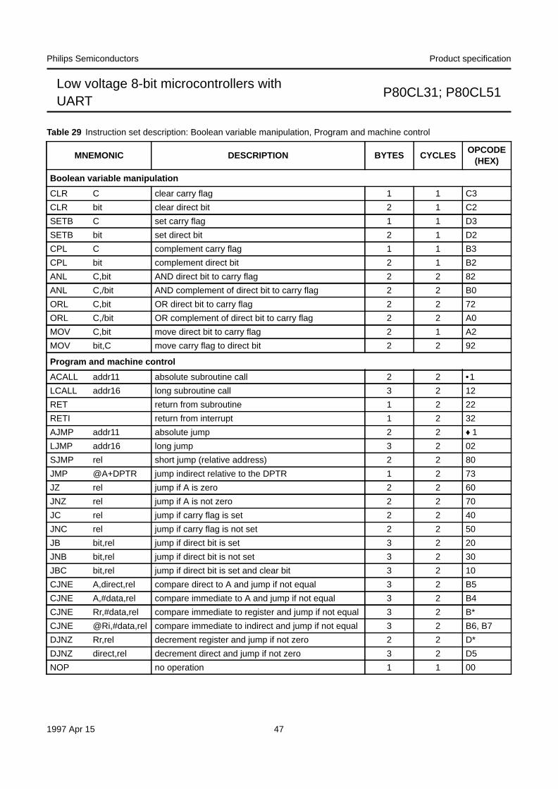
Table 29 Instruction set description: Boolean variable manipulation, Program and machine control
MNEMONIC DESCRIPTION BYTES CYCLESOPCODE
(HEX)
Boolean variable manipulation
CLR C clear carry flag 1 1 C3
CLR bit clear direct bit 2 1 C2
SETB C set carry flag 1 1 D3
SETB bit set direct bit 2 1 D2
CPL C complement carry flag 1 1 B3
CPL bit complement direct bit 2 1 B2
ANL C,bit AND direct bit to carry flag 2 2 82
ANL C,/bit AND complement of direct bit to carry flag 2 2 B0
ORL C,bit OR direct bit to carry flag 2 2 72
ORL C,/bit OR complement of direct bit to carry flag 2 2 A0
MOV C,bit move direct bit to carry flag 2 1 A2
MOV bit,C move carry flag to direct bit 2 2 92
Program and machine control
ACALL addr11 absolute subroutine call 2 2 · 1
LCALL addr16 long subroutine call 3 2 12
RET return from subroutine 1 2 22
RETI return from interrupt 1 2 32
AJMP addr11 absolute jump 2 2 ¨ 1
LJMP addr16 long jump 3 2 02
SJMP rel short jump (relative address) 2 2 80
JMP @A+DPTR jump indirect relative to the DPTR 1 2 73
JZ rel jump if A is zero 2 2 60
JNZ rel jump if A is not zero 2 2 70
JC rel jump if carry flag is set 2 2 40
JNC rel jump if carry flag is not set 2 2 50
JB bit,rel jump if direct bit is set 3 2 20
JNB bit,rel jump if direct bit is not set 3 2 30
JBC bit,rel jump if direct bit is set and clear bit 3 2 10
CJNE A,direct,rel compare direct to A and jump if not equal 3 2 B5
CJNE A,#data,rel compare immediate to A and jump if not equal 3 2 B4
CJNE Rr,#data,rel compare immediate to register and jump if not equal 3 2 B*
CJNE @Ri,#data,rel compare immediate to indirect and jump if not equal 3 2 B6, B7
DJNZ Rr,rel decrement register and jump if not zero 2 2 D*
DJNZ direct,rel decrement direct and jump if not zero 3 2 D5
NOP no operation 1 1 00

1997 Apr 15 48
Philips Semiconductors Product specification
Low voltage 8-bit microcontrollers withUART
P80CL31; P80CL51
Table 30 Description of the mnemonics in the Instruction set
MNEMONIC DESCRIPTION
Data addressing modes
Rr working register R0-R7
direct 128 internal RAM locations and any special function register (SFR)
@Ri indirect internal RAM location addressed by register R0 or R1 of the actual register bank
#data 8-bit constant included in instruction
#data 16 16-bit constant included as bytes 2 and 3 of instruction
bit direct addressed bit in internal RAM or SFR.
addr16 16-bit destination address. Used by LCALL and LJMP;the branch will be anywhere within the 64 kbytes Program Memory address space
addr11 111-bit destination address. Used by ACALL and AJMP. The branch will be within the same 2 kbytespage of Program Memory as the first byte of the following instruction
rel signed (two's complement) 8-bit offset byte. Used by SJMP and all conditional jumps;range is - 128 to +127 bytes relative to first byte of the following instruction
Hexadecimal opcode cross-reference
* 8, 9, A, B, C, D, E, F
· 1, 3, 5, 7, 9, B, D, F
¨ 0, 2, 4, 6, 8, A, C, E
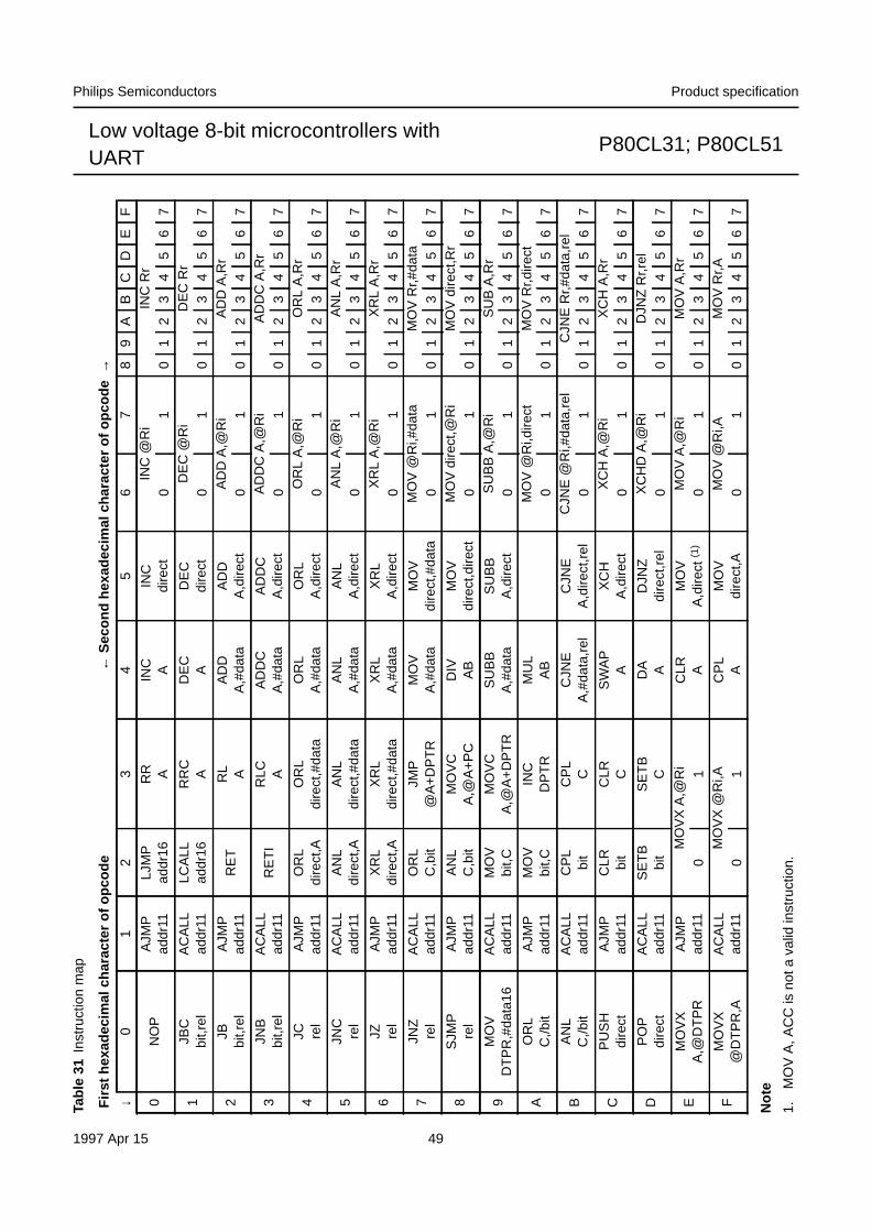
1997 Apr 15 49
Philips Semiconductors Product specification
Low voltage 8-bit microcontrollers withUART
P80CL31; P80CL51
Tabl
e 31
Inst
ruct
ion
map
Not
e
1.M
OV
A, A
CC
is n
ot a
val
id in
stru
ctio
n.
Firs
t hex
adec
imal
cha
ract
er o
f opc
ode
¬ S
econ
d he
xade
cim
al c
hara
cter
of o
pcod
e ®
¯0
12
34
56
78
9A
BC
DE
F
0N
OP
AJM
Pad
dr11
LJM
Pad
dr16
RR A
INC A
INC
dire
ctIN
C @
Ri
INC
Rr
01
01
23
45
67
1JB
Cbi
t,rel
AC
ALL
addr
11LC
ALL
addr
16R
RC
AD
EC
AD
EC
dire
ctD
EC
@R
iD
EC
Rr
01
01
23
45
67
2JB
bit,r
elA
JMP
addr
11R
ET
RL A
AD
DA
,#da
taA
DD
A,d
irect
AD
D A
,@R
iA
DD
A,R
r0
10
12
34
56
7
3JN
Bbi
t,rel
AC
ALL
addr
11R
ET
IR
LC AA
DD
CA
,#da
taA
DD
CA
,dire
ctA
DD
C A
,@R
iA
DD
C A
,Rr
01
01
23
45
67
4JC re
lA
JMP
addr
11O
RL
dire
ct,A
OR
Ldi
rect
,#da
taO
RL
A,#
data
OR
LA
,dire
ctO
RL
A,@
Ri
OR
L A
,Rr
01
01
23
45
67
5JN
Cre
lA
CA
LLad
dr11
AN
Ldi
rect
,AA
NL
dire
ct,#
data
AN
LA
,#da
taA
NL
A,d
irect
AN
L A
,@R
iA
NL
A,R
r0
10
12
34
56
7
6JZ re
lA
JMP
addr
11X
RL
dire
ct,A
XR
Ldi
rect
,#da
taX
RL
A,#
data
XR
LA
,dire
ctX
RL
A,@
Ri
XR
L A
,Rr
01
01
23
45
67
7JN
Zre
lA
CA
LLad
dr11
OR
LC
,bit
JMP
@A
+D
PT
RM
OV
A,#
data
MO
Vdi
rect
,#da
taM
OV
@R
i,#da
taM
OV
Rr,#
data
01
01
23
45
67
8S
JMP
rel
AJM
Pad
dr11
AN
LC
,bit
MO
VC
A,@
A+
PC
DIV AB
MO
Vdi
rect
,dire
ctM
OV
dire
ct,@
Ri
MO
V d
irect
,Rr
01
01
23
45
67
9M
OV
DT
PR
,#da
ta16
AC
ALL
addr
11M
OV
bit,C
MO
VC
A,@
A+
DP
TR
SU
BB
A,#
data
SU
BB
A,d
irect
SU
BB
A,@
Ri
SU
B A
,Rr
01
01
23
45
67
AO
RL
C,/b
itA
JMP
addr
11M
OV
bit,C
INC
DP
TR
MU
LA
BM
OV
@R
i,dire
ctM
OV
Rr,d
irect
01
01
23
45
67
BA
NL
C,/b
itA
CA
LLad
dr11
CP
Lbi
tC
PL
CC
JNE
A,#
data
,rel
CJN
EA
,dire
ct,r
elC
JNE
@R
i,#da
ta,r
elC
JNE
Rr,#
data
,rel
01
01
23
45
67
CP
US
Hdi
rect
AJM
Pad
dr11
CLR bit
CLR C
SW
AP
AX
CH
A,d
irect
XC
H A
,@R
iX
CH
A,R
r0
10
12
34
56
7
DP
OP
dire
ctA
CA
LLad
dr11
SE
TB
bit
SE
TB
CD
A AD
JNZ
dire
ct,r
elX
CH
D A
,@R
iD
JNZ
Rr,r
el0
10
12
34
56
7
EM
OV
XA
,@D
TP
RA
JMP
addr
11M
OV
X A
,@R
iC
LR AM
OV
A,d
irect
(1)
MO
V A
,@R
iM
OV
A,R
r0
10
10
12
34
56
7
FM
OV
X@
DT
PR
,AA
CA
LLad
dr11
MO
VX
@R
i,AC
PL
AM
OV
dire
ct,A
MO
V @
Ri,A
MO
V R
r,A0
10
10
12
34
56
7

1997 Apr 15 50
Philips Semiconductors Product specification
Low voltage 8-bit microcontrollers withUART
P80CL31; P80CL51
20 LIMITING VALUESIn accordance with the Absolute Maximum Rating System (IEC 134).
21 DC CHARACTERISTICS FOR P80CL31 AND P80CL51VSS = 0 V; Tamb = - 40 to +85 °C; all voltages with respect to VSS unless otherwise specified.
SYMBOL PARAMETER MIN. MAX. UNIT
VDD supply voltage - 0.5 +6.5 V
VI input voltage on any pin with respect to ground (VSS) - 0.5 VDD + 0.5 V
II DC current on any input - 5.0 +5.0 mA
IO DC current on any output - 5.0 +5.0 mA
Ptot total power dissipation - 300 mW
Tstg storage temperature - 65 +150 °CTamb operating ambient temperature - 40 +85 °CTj operating junction temperature - +125 °C
SYMBOL PARAMETER CONDITIONS MIN. MAX. UNIT
VDD supply voltage
operating VSS = 0 V 1.8 6.0 V
RAM retention in Power-downmode
1.0 - V
Supply current (note 1, note 2)
IDD operating supply current Oscillator 1; fclk = 32 kHz; VDD = 1.8 V;Tamb = 25 °C
- 50 m A
Oscillator 2; fclk = 3.58 MHz; VDD = 3 V - 2.5 mA
Oscillator 3; fclk = 16 MHz; VDD = 5 V - 24 mA
Oscillator 4; fclk = 16 MHz; VDD = 5 V - 26 mA
Supply current (Idle mode) (note 2, note 3)
IDD(idle) supply current (Idle mode) Oscillator 1; fclk = 32 kHz; VDD = 1.8 V;Tamb = 25 °C
- 25 m A
Oscillator 2; fclk = 3.58 MHz; VDD = 3 V - 1.0 mA
Oscillator 3; fclk = 16 MHz; VDD = 5 V - 10 mA
Oscillator 4; fclk = 16 MHz; VDD = 5 V - 12 mA
Supply current (Power-down mode) (note 2, note 4)
IDD(pd) supply current (Power-down mode) VDD = 1.8 V; Tamb = 25 °C - 10 m A
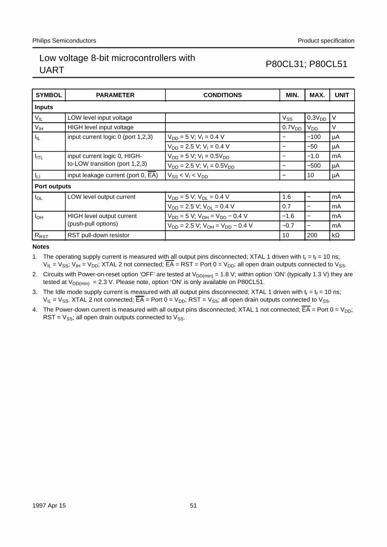
1997 Apr 15 51
Philips Semiconductors Product specification
Low voltage 8-bit microcontrollers withUART
P80CL31; P80CL51
Notes
1. The operating supply current is measured with all output pins disconnected; XTAL 1 driven with tr = tf = 10 ns;VIL = VSS; VIH = VDD; XTAL 2 not connected; EA = RST = Port 0 = VDD; all open drain outputs connected to VSS.
2. Circuits with Power-on-reset option ‘OFF’ are tested at VDD(min) = 1.8 V; within option ‘ON’ (typically 1.3 V) they aretested at VDD(min) = 2.3 V. Please note, option ‘ON’ is only available on P80CL51.
3. The Idle mode supply current is measured with all output pins disconnected; XTAL 1 driven with tr = tf = 10 ns;VIL = VSS. XTAL 2 not connected; EA = Port 0 = VDD; RST = VSS; all open drain outputs connected to VSS.
4. The Power-down current is measured with all output pins disconnected; XTAL 1 not connected; EA = Port 0 = VDD;RST = VSS; all open drain outputs connected to VSS.
Inputs
VIL LOW level input voltage VSS 0.3VDD V
VIH HIGH level input voltage 0.7VDD VDD V
IIL input current logic 0 (port 1,2,3) VDD = 5 V; VI = 0.4 V - - 100 m A
VDD = 2.5 V; VI = 0.4 V - - 50 m A
IITL input current logic 0, HIGH-to-LOW transition (port 1,2,3)
VDD = 5 V; VI = 0.5VDD - - 1.0 mA
VDD = 2.5 V; VI = 0.5VDD - - 500 m A
ILI input leakage current (port 0, EA) VSS < VI < VDD - 10 m A
Port outputs
IOL LOW level output current VDD = 5 V; VOL = 0.4 V 1.6 - mA
VDD = 2.5 V; VOL = 0.4 V 0.7 - mA
IOH HIGH level output current(push-pull options)
VDD = 5 V; VOH = VDD - 0.4 V - 1.6 - mA
VDD = 2.5 V; VOH = VDD - 0.4 V - 0.7 - mA
RRST RST pull-down resistor 10 200 kW
SYMBOL PARAMETER CONDITIONS MIN. MAX. UNIT

1997 Apr 15 52
Philips Semiconductors Product specification
Low voltage 8-bit microcontrollers withUART
P80CL31; P80CL51
22 DC CHARACTERISTICS FOR P80C51VSS = 0 V; VDD = 5.0V ±10%; fclk = 3.5 to 16 MHz; Tamb = - 40 to +85 °C all voltages with respect to VSS unlessotherwise specified. Note that the Power-on-reset option is ‘OFF’ and the Oscillator option is ‘Oscillator 3’.
Notes
1. The operating supply current is measured with all output pins disconnected; XTAL 1 driven with tr = tf = 10 ns;VIL = VSS; VIH = VDD; XTAL 2 not connected; EA = RST = Port 0 = VDD; all open drain outputs connected to VSS.
2. The Idle mode supply current is measured with all output pins disconnected; XTAL 1 driven with tr = tf = 10 ns;VIL = VSS. XTAL 2 not connected; EA = Port 0 = VDD; RST = VSS; all open drain outputs connected to VSS.
3. The Power-down current is measured with all output pins disconnected; XTAL 1 not connected; EA = Port 0 = VDD;RST = VSS; all open drain outputs connected to VSS.
SYMBOL PARAMETER CONDITIONS MIN. MAX. UNIT
VDD supply voltage
operating VSS = 0 V 4.5 5.5 V
RAM retention in Power-downmode
1.0 - V
IDD operating supply current fclk = 16 MHz; VDD = 5.0 V; note 1 - 24 mA
IDD(idle) supply current (Idle mode) fclk = 16 MHz; VDD = 5.0 V; note 2 - 10 mA
IDD(pd) supply current (Power-down mode) VDD = 5.0 V; note 3 - 50 mA
Inputs
VIL LOW level input voltage VSS 0.3VDD V
VIH HIGH level input voltage 0.7VDD VDD V
IIL input current logic 0 (port 1,2,3) VI = 0.4 V - 100 m A
ITL input current logic 0, HIGH- to-LOWtransition (port 1,2,3)
VI = 0.5VDD - 1.0 mA
ILI input leakage current (port 0, EA) VSS < VI < VDD - 10 m A
Port outputs
IOL LOW level output current VOL = 0.4 V 1.6 - mA
IOH HIGH level output current (push-pulloptions)
VOH = VDD - 0.4 V - 1.6 - mA
RRST RST pull-down resistor 10 200 kW

1997 Apr 15 53
Philips Semiconductors Product specification
Low voltage 8-bit microcontrollers withUART
P80CL31; P80CL51
Fig.28 Frequency operating range.
handbook, halfpage
0 2
fXTAL (MHz)
4 6VDD (V)
20
0
16
12
8
4
MBK035
Fig.29 Typical operating current as a function offrequency and VDD.
Tamb = 25 °C.
handbook, halfpage
0 2 4
IDD (mA)
6VDD (V)
20
16
12
4
0
8
MBK036
3.58 MHz
8 MHz
12 MHz
16 MHz
Fig.30 Typical Idle current as a function offrequency and VDD.
Tamb = 25 °C.
handbook, halfpage
0 VDD (V)2 4
16 MHz
12 MHz
IDD (idle)
6
6
0
2
4
MBK046
8 MHz
3.58 MHz
Fig.31 Typical Power-down current as a function ofVDD.
handbook, halfpage
0 2 4 6
6
4
0
2
MLA592
IDD(pd) (m A)
VDD (V)
Tamb = 25 °C.

1997 Apr 15 54
Philips Semiconductors Product specification
Low voltage 8-bit microcontrollers withUART
P80CL31; P80CL51
23 AC CHARACTERISTICSVDD = 5 V; VSS = 0 V; Tamb = - 40 to +85 °C; CL = 50 pF for Port 0, ALE and PSEN; CL = 40 pF for all other outputsunless specified; tCLK = 1/ fCLK.
SYMBOL PARAMETERfosc = 12 MHz fosc = VARIABLE
UNITMIN. MAX. MIN. MAX.
Program Memory (Fig.32)
tLHLL ALE pulse width 127 - 2tCLK - 40 - ns
tAVLL address valid to ALE LOW 43 - tCLK - 40 - ns
tLLAX address hold after ALE LOW 48 - tCLK - 35 - ns
tLLIV ALE LOW to valid instruction in - 233 - 4tCLK - 100 ns
tLLPL ALE LOW to PSEN LOW 58 - tCLK - 25 - ns
tPLPH PSEN pulse width 215 - 3tCLK - 35 - ns
tPLIV PSEN LOW to valid instruction in - 125 - 3tCLK - 125 ns
tPXIX input instruction hold after PSEN 0 - 0 - ns
tPXIZ input instruction float after PSEN - 63 - tCLK - 20 ns
tPXAV PSEN to address valid 75 - tCLK - 8 - ns
tAVIV address to valid instruction in - 302 - 5tCLK - 115 ns
tPLAZ PSEN LOW to address float 12 - 0 - ns
External Data Memory (Figs 33 and 34)
tRLRH RD pulse width 400 - 6tCLK - 100 - ns
tWLWH WR pulse width 400 - 6tCLK - 100 - ns
tLLAX address hold after ALE LOW 48 - tCLK - 35 - ns
tRLDV RD LOW to valid data in - 150 - 5tCLK - 165 ns
tRHDZ data float after RD - 97 - 2tCLK - 70 ns
tLLDV ALE LOW to valid data in - 517 8tCLK - 150 ns
tAVDV address to valid data in - 585 - 9tCLK - 165 ns
tLLWL ALE LOW to RD or WR LOW 200 300 3tCLK - 50 3tCLK + 50 ns
tAVWL address valid to RD or WR LOW 203 - 4 - ns
tWHLH RD or WR HIGH to ALE HIGH 43 123 tCLK - 40 tCLK + 40 ns
tQVWX data valid to WR transition 23 - tCLK - 60 - ns
tQVWH data valid time WR HIGH 433 - 7tCLK - 150 - ns
tWHQX data hold after WR 33 - tCLK - 50 - ns
tRLAZ RD LOW to address float - 12 - 12 ns

1997 Apr 15 55
Philips Semiconductors Product specification
Low voltage 8-bit microcontrollers withUART
P80CL31; P80CL51
Fig.32 Read from Program Memory.
handbook, full pagewidth
MGD680
t LHLL
ALE
PORT 0
PORT 2
t CY
LLIVt
t LLPL
t PLPH
t LLAX
tAVLL
AVIVt
PLAZt
PLIVt
t PXIX
t PXIZ
t PXAV
address A8 to A15 address A8 to A15
inst. inputinst. input A0 to A7A0 to A7
PSEN
handbook, full pagewidth
MGA177
t LHLL
ALE
PORT 0
PORT 2
t CY
t LLDV
t LLAXt AVLL
AVDVt
RLAZt
address A8 to A15 (DPH) or Port 2
data inputA0 to A7
PSEN
tWHLH
AVWLt
t LLWL t RLRH
t RHDX
t RHDZ
t RLDV
RD
Fig.33 Read from Data Memory.

1997 Apr 15 56
Philips Semiconductors Product specification
Low voltage 8-bit microcontrollers withUART
P80CL31; P80CL51
Fig.34 Write to Data Memory.
handbook, full pagewidth
MGA178
t LHLL
ALE
PORT 0
PORT 2
t CY
t LLAXtAVLL
address A8 to A15 (DPH) or Port 2
data outputA0 to A7
PSEN
tWHLH
AVWLt
t LLWL t WLWH
t WHQXt QVWH
t QVWX
WR

1997 Apr 15 57
Philips Semiconductors Product specification
Low voltage 8-bit microcontrollers withUART
P80CL31; P80CL51
Fig.35 Instruction cycle timing.
handbook, full pagewidth
MGD681
P1 P2S1
P1 P2S2
P1 P2S3
P1 P2S4
P1 P2S5
P1 P2S6
P1 P2S1
P1 P2S2
P1 P2S3
P1 P2S4
P1 P2S5
P1 P2S6
one machine cycle one machine cycle
XTAL1 INPUT
address A0 - A7
inst. in
address A0 - A7
inst. in
address A0 - A7
inst. in
address A0 - A7
inst. in
address A8 - A15address A8 - A15address A8 - A15address A8 - A15
address A0 - A7
inst. in
address A0 - A7
inst. in
address A0 - A7
data output or data input
address A8 - A15address A8 - A15 or Port 2 outputaddress A8 - A15
old data new data
sampling time of I/O port pins during input
SERIAL PORT SHIFT CLOCK (MODE 0)
PORT 0, 2, 3 INPUT
PORT 0, 2, 3 OUTPUT
PORT 2
BUS (PORT 0)read or
write of external data
memory
PORT 2
BUS (PORT 0)
external program memory
fetch
WR
RD
only active during a write
to external data memory
only active during a read from external data memory
PSEN
ALE
dotted lines are valid when RD or WR are
active
old data new dataPORT 1 OUTPUT

1997 Apr 15 58
Philips Semiconductors Product specification
Low voltage 8-bit microcontrollers withUART
P80CL31; P80CL51
Fig.36 AC testing input waveform.
handbook, halfpage
MLA586
0.9 V
0.4 V
0.7 V
0.3 V
0.7 V
0.3 V
test points
DD
DD
DD
DD DD
DD
Fig.37 Input current.
handbook, 4 columns MGD682
0.5 VDD VDD
- 100 m A
- 500 m A
IIL
IL
IIL(T)
1997 Apr 15 59
Philips Semiconductors Product specification
Low voltage 8-bit microcontrollers withUART
P80CL31; P80CL51
24 P85CL000HFZ ‘PIGGY-BACK’ SPECIFICATION
The differences between the masked version and thepiggy-back are described below.
24.1 General description
The P85CL000HFZ is a piggy-back version with 256 bytesof RAM used for emulation of the P80CL51 and theP83CL410 microcontrollers. The P85CL000HFZ ismanufactured in an advanced CMOS technology.The instruction set of the P85CL000HFZ is based on thatof the 8051. The device has low power consumption and awide supply voltage range. The P85CL000HFZ has twosoftware selectable modes of reduced activity for furtherpower reduction: Idle and Power-down. For timing andAC/DC characteristics, please refer to the P80CL51specifications.
24.2 Feature differences/additional features withrespect to P80CL51
· No internal ROM
· 8-bit CPU, RAM, I/O in a single 40-lead package withDIP pin-out
· Socket for up to 16 kbytes external EPROM
· 256 bytes RAM, expandable externally to 64 kbytes
· I2C-bus interface for serial transfer on two lines
· On-chip oscillator: Oscillator 4 option only.
24.3 Common specification/feature differences between P85CL000HFZ and P83CL410/P80CL51
PARAMETER P83CL410/P80CL51 P85CL000HFZ ‘PIGGY-BACK’
RAM size 128 256
ROM size 4K EPROM size dependent (max. 16K)
Port options 1, 2, 3 1
Oscillator options Oscillator 1, 2, 3, 4, RC Oscillator 4
Mechanical dimensions standard dual in-line, small outline same pin-out as SOT129-1, but largerpackage size
Current consumption IDD IDD (Oscillator 4) + IEPROM
Voltage range full full, limited by EPROM
ESD specification not tested (different package)

1997 Apr 15 60
Philips Semiconductors Product specification
Low voltage 8-bit microcontrollers withUART
P80CL31; P80CL51
25 PACKAGE OUTLINES
UNIT Amax.
1 2 b1 c D E e MHL
REFERENCESOUTLINEVERSION
EUROPEANPROJECTION ISSUE DATE
IEC JEDEC EIAJ
mm
inches
DIMENSIONS (inch dimensions are derived from the original mm dimensions)
SOT129-192-11-1795-01-14
A min.
A max. b Z
max.wMEe1
1.701.14
0.530.38
0.360.23
52.5051.50
14.113.7
3.603.05 0.2542.54 15.24
15.8015.24
17.4215.90 2.254.7 0.51 4.0
0.0670.045
0.0210.015
0.0140.009
2.0672.028
0.560.54
0.140.12 0.010.10 0.60
0.620.60
0.690.63 0.089 0.19 0.020 0.16
051G08 MO-015AJ
MH
c
(e )1
ME
A
L
seat
ing
plan
e
A1
w Mb1
e
D
A2
Z
40
1
21
20
b
E
pin 1 index
0 5 10 mm
scale
Note
1. Plastic or metal protrusions of 0.25 mm maximum per side are not included.
(1)(1)(1)
DIP40: plastic dual in-line package; 40 leads (600 mil) SOT129-1

1997 Apr 15 61
Philips Semiconductors Product specification
Low voltage 8-bit microcontrollers withUART
P80CL31; P80CL51
UNIT A1 A2 A3 bp c D(1) E(2) Z(1)e HE L Lp Q ywv q
REFERENCESOUTLINE VERSION
EUROPEAN PROJECTION ISSUE DATE
IEC JEDEC EIAJ
mm
inches
0.3 0.1
2.45 2.25 0.25
0.42 0.30
0.22 0.14
15.6 15.2
7.6 7.5 0.762 2.25
12.3 11.8
1.15 1.05
0.6 0.3 7
0
o
o
0.1 0.1
DIMENSIONS (inch dimensions are derived from the original mm dimensions)
Notes
1. Plastic or metal protrusions of 0.4 mm maximum per side are not included.
2. Plastic interlead protrusions of 0.25 mm maximum per side are not included.
1.7 1.5
SOT158-192-11-17 95-01-24
X
w M
q
AA1
A2
bp
D
HE
Lp
Q
detail X
E
Z
e
c
L
v M A
(A )3
A
y
40
20
21
1
pin 1 index
0.012 0.004
0.096 0.089
0.017 0.012
0.0087 0.0055
0.61 0.60
0.30 0.29 0.03 0.089
0.48 0.46
0.045 0.041
0.024 0.0120.004
0.2
0.008 0.0040.067 0.0590.010
0 5 10 mm
scale
VSO40: plastic very small outline package; 40 leads SOT158-1
A max.
2.70
0.11

1997 Apr 15 62
Philips Semiconductors Product specification
Low voltage 8-bit microcontrollers withUART
P80CL31; P80CL51
UNIT A1 A2 A3 bp c E(1) e HE L Lp Q Zywv q
REFERENCESOUTLINEVERSION
EUROPEANPROJECTION ISSUE DATE
IEC JEDEC EIAJ
mm 0.250.05
1.851.65 0.25
0.400.20
0.250.14
10.19.9 0.8 1.3
12.912.3
0.850.75
1.20.8
100
o
o0.15 0.10.15
DIMENSIONS (mm are the original dimensions)
Note
1. Plastic or metal protrusions of 0.25 mm maximum per side are not included.
0.950.55
SOT307-292-11-1795-02-04
D(1) (1)(1)
10.19.9
HD
12.912.3
EZ
1.20.8
D
e
E
B
11
c
EH
D
ZD
A
ZE
e
v M A
X
1
44
34
33 23
22
12
y
q
A1A
Lp
Q
detail X
L
(A )3A2
pin 1 index
DH v M B
bp
bp
w M
w M
0 2.5 5 mm
scale
QFP44: plastic quad flat package; 44 leads (lead length 1.3 mm); body 10 x 10 x 1.75 mm SOT307-2
Amax.
2.10

1997 Apr 15 63
Philips Semiconductors Product specification
Low voltage 8-bit microcontrollers withUART
P80CL31; P80CL51
26 SOLDERING
26.1 Introduction
There is no soldering method that is ideal for all ICpackages. Wave soldering is often preferred whenthrough-hole and surface mounted components are mixedon one printed-circuit board. However, wave soldering isnot always suitable for surface mounted ICs, or forprinted-circuits with high population densities. In thesesituations reflow soldering is often used.
This text gives a very brief insight to a complex technology.A more in-depth account of soldering ICs can be found inour “IC Package Databook” (order code 9398 652 90011).
26.2 DIP
26.2.1 SOLDERING BY DIPPING OR BY WAVE
The maximum permissible temperature of the solder is260 °C; solder at this temperature must not be in contactwith the joint for more than 5 seconds. The total contacttime of successive solder waves must not exceed5 seconds.
The device may be mounted up to the seating plane, butthe temperature of the plastic body must not exceed thespecified maximum storage temperature (Tstg max). If theprinted-circuit board has been pre-heated, forced coolingmay be necessary immediately after soldering to keep thetemperature within the permissible limit.
26.2.2 REPAIRING SOLDERED JOINTS
Apply a low voltage soldering iron (less than 24 V) to thelead(s) of the package, below the seating plane or notmore than 2 mm above it. If the temperature of thesoldering iron bit is less than 300 °C it may remain incontact for up to 10 seconds. If the bit temperature isbetween 300 and 400 °C, contact may be up to 5 seconds.
26.3 QFP and VSO
26.3.1 REFLOW SOLDERING
Reflow soldering techniques are suitable for all QFP andVSO packages.
The choice of heating method may be influenced by largerplastic QFP packages (44 leads, or more). If infrared orvapour phase heating is used and the large packages arenot absolutely dry (less than 0.1% moisture content byweight), vaporization of the small amount of moisture inthem can cause cracking of the plastic body. For moreinformation, refer to the Drypack chapter in our “QualityReference Manual” (order code 9397 750 00192).
Reflow soldering requires solder paste (a suspension offine solder particles, flux and binding agent) to be appliedto the printed-circuit board by screen printing, stencilling orpressure-syringe dispensing before package placement.
Several techniques exist for reflowing; for example,thermal conduction by heated belt. Dwell times varybetween 50 and 300 seconds depending on heatingmethod. Typical reflow temperatures range from215 to 250 °C.
Preheating is necessary to dry the paste and evaporatethe binding agent. Preheating duration: 45 minutes at45 °C.
26.3.2 WAVE SOLDERING
26.3.2.1 QFP
Wave soldering is not recommended for QFP packages.This is because of the likelihood of solder bridging due toclosely-spaced leads and the possibility of incompletesolder penetration in multi-lead devices.
If wave soldering cannot be avoided, the followingconditions must be observed:
· A double-wave (a turbulent wave with high upwardpressure followed by a smooth laminar wave)soldering technique should be used.
· The footprint must be at an angle of 45 ° to the boarddirection and must incorporate solder thievesdownstream and at the side corners.
Even with these conditions, do not consider wavesoldering the following packages: QFP52 (SOT379-1),QFP100 (SOT317-1), QFP100 (SOT317-2),QFP100 (SOT382-1) or QFP160 (SOT322-1).
26.3.2.2 VSO
Wave soldering techniques can be used for all VSOpackages if the following conditions are observed:
· A double-wave (a turbulent wave with high upwardpressure followed by a smooth laminar wave) solderingtechnique should be used.
· The longitudinal axis of the package footprint must beparallel to the solder flow.
· The package footprint must incorporate solder thieves atthe downstream end.

1997 Apr 15 64
Philips Semiconductors Product specification
Low voltage 8-bit microcontrollers withUART
P80CL31; P80CL51
26.3.2.3 Method (QFP and VSO)
During placement and before soldering, the package mustbe fixed with a droplet of adhesive. The adhesive can beapplied by screen printing, pin transfer or syringedispensing. The package can be soldered after theadhesive is cured.
Maximum permissible solder temperature is 260 °C, andmaximum duration of package immersion in solder is10 seconds, if cooled to less than 150 °C within6 seconds. Typical dwell time is 4 seconds at 250 °C.
A mildly-activated flux will eliminate the need for removalof corrosive residues in most applications.
26.3.3 REPAIRING SOLDERED JOINTS
Fix the component by first soldering two diagonally-opposite end leads. Use only a low voltage soldering iron(less than 24 V) applied to the flat part of the lead. Contacttime must be limited to 10 seconds at up to 300 °C. Whenusing a dedicated tool, all other leads can be soldered inone operation within 2 to 5 seconds between270 and 320 °C.
27 DEFINITIONS
28 LIFE SUPPORT APPLICATIONS
These products are not designed for use in life support appliances, devices, or systems where malfunction of theseproducts can reasonably be expected to result in personal injury. Philips customers using or selling these products foruse in such applications do so at their own risk and agree to fully indemnify Philips for any damages resulting from suchimproper use or sale.
Data sheet status
Objective specification This data sheet contains target or goal specifications for product development.
Preliminary specification This data sheet contains preliminary data; supplementary data may be published later.
Product specification This data sheet contains final product specifications.
Limiting values
Limiting values given are in accordance with the Absolute Maximum Rating System (IEC 134). Stress above one ormore of the limiting values may cause permanent damage to the device. These are stress ratings only and operationof the device at these or at any other conditions above those given in the Characteristics sections of the specificationis not implied. Exposure to limiting values for extended periods may affect device reliability.
Application information
Where application information is given, it is advisory and does not form part of the specification.

1997 Apr 15 65
Philips Semiconductors Product specification
Low voltage 8-bit microcontrollers withUART
P80CL31; P80CL51
NOTES

1997 Apr 15 66
Philips Semiconductors Product specification
Low voltage 8-bit microcontrollers withUART
P80CL31; P80CL51
NOTES

1997 Apr 15 67
Philips Semiconductors Product specification
Low voltage 8-bit microcontrollers withUART
P80CL31; P80CL51
NOTES

Internet: http://www.semiconductors.philips.com
Philips Semiconductors – a worldwide company
© Philips Electronics N.V. 1997 SCA54
All rights are reserved. Reproduction in whole or in part is prohibited without the prior written consent of the copyright owner.
The information presented in this document does not form part of any quotation or contract, is believed to be accurate and reliable and may be changedwithout notice. No liability will be accepted by the publisher for any consequence of its use. Publication thereof does not convey nor imply any licenseunder patent- or other industrial or intellectual property rights.
Netherlands: Postbus 90050, 5600 PB EINDHOVEN, Bldg. VB,Tel. +31 40 27 82785, Fax. +31 40 27 88399
New Zealand: 2 Wagener Place, C.P.O. Box 1041, AUCKLAND,Tel. +64 9 849 4160, Fax. +64 9 849 7811
Norway: Box 1, Manglerud 0612, OSLO,Tel. +47 22 74 8000, Fax. +47 22 74 8341
Philippines: Philips Semiconductors Philippines Inc.,106 Valero St. Salcedo Village, P.O. Box 2108 MCC, MAKATI,Metro MANILA, Tel. +63 2 816 6380, Fax. +63 2 817 3474
Poland: Ul. Lukiska 10, PL 04-123 WARSZAWA,Tel. +48 22 612 2831, Fax. +48 22 612 2327
Portugal: see Spain
Romania: see Italy
Russia: Philips Russia, Ul. Usatcheva 35A, 119048 MOSCOW,Tel. +7 095 755 6918, Fax. +7 095 755 6919
Singapore: Lorong 1, Toa Payoh, SINGAPORE 1231,Tel. +65 350 2538, Fax. +65 251 6500
Slovakia: see Austria
Slovenia: see Italy
South Africa: S.A. PHILIPS Pty Ltd., 195-215 Main Road Martindale,2092 JOHANNESBURG, P.O. Box 7430 Johannesburg 2000,Tel. +27 11 470 5911, Fax. +27 11 470 5494
South America: Rua do Rocio 220, 5th floor, Suite 51,04552-903 São Paulo, SÃO PAULO - SP, Brazil,Tel. +55 11 821 2333, Fax. +55 11 829 1849
Spain: Balmes 22, 08007 BARCELONA,Tel. +34 3 301 6312, Fax. +34 3 301 4107
Sweden: Kottbygatan 7, Akalla, S-16485 STOCKHOLM,Tel. +46 8 632 2000, Fax. +46 8 632 2745
Switzerland: Allmendstrasse 140, CH-8027 ZÜRICH,Tel. +41 1 488 2686, Fax. +41 1 481 7730
Taiwan: Philips Semiconductors, 6F, No. 96, Chien Kuo N. Rd., Sec. 1,TAIPEI, Taiwan Tel. +886 2 2134 2865, Fax. +886 2 2134 2874
Thailand: PHILIPS ELECTRONICS (THAILAND) Ltd.,209/2 Sanpavuth-Bangna Road Prakanong, BANGKOK 10260,Tel. +66 2 745 4090, Fax. +66 2 398 0793
Turkey: Talatpasa Cad. No. 5, 80640 GÜLTEPE/ISTANBUL,Tel. +90 212 279 2770, Fax. +90 212 282 6707
Ukraine : PHILIPS UKRAINE, 4 Patrice Lumumba str., Building B, Floor 7,252042 KIEV, Tel. +380 44 264 2776, Fax. +380 44 268 0461
United Kingdom: Philips Semiconductors Ltd., 276 Bath Road, Hayes,MIDDLESEX UB3 5BX, Tel. +44 181 730 5000, Fax. +44 181 754 8421
United States: 811 East Arques Avenue, SUNNYVALE, CA 94088-3409,Tel. +1 800 234 7381
Uruguay: see South America
Vietnam: see Singapore
Yugoslavia: PHILIPS, Trg N. Pasica 5/v, 11000 BEOGRAD,Tel. +381 11 625 344, Fax.+381 11 635 777
For all other countries apply to: Philips Semiconductors, Marketing & Sales Communications,Building BE-p, P.O. Box 218, 5600 MD EINDHOVEN, The Netherlands, Fax. +31 40 27 24825
Argentina: see South America
Australia: 34 Waterloo Road, NORTH RYDE, NSW 2113,Tel. +61 2 9805 4455, Fax. +61 2 9805 4466
Austria: Computerstr. 6, A-1101 WIEN, P.O. Box 213,Tel. +43 1 60 101, Fax. +43 1 60 101 1210
Belarus: Hotel Minsk Business Center, Bld. 3, r. 1211, Volodarski Str. 6,220050 MINSK, Tel. +375 172 200 733, Fax. +375 172 200 773
Belgium: see The Netherlands
Brazil: see South America
Bulgaria: Philips Bulgaria Ltd., Energoproject, 15th floor,51 James Bourchier Blvd., 1407 SOFIA,Tel. +359 2 689 211, Fax. +359 2 689 102
Canada: PHILIPS SEMICONDUCTORS/COMPONENTS,Tel. +1 800 234 7381
China/Hong Kong: 501 Hong Kong Industrial Technology Centre,72 Tat Chee Avenue, Kowloon Tong, HONG KONG,Tel. +852 2319 7888, Fax. +852 2319 7700
Colombia: see South America
Czech Republic: see Austria
Denmark: Prags Boulevard 80, PB 1919, DK-2300 COPENHAGEN S,Tel. +45 32 88 2636, Fax. +45 31 57 0044
Finland: Sinikalliontie 3, FIN-02630 ESPOO,Tel. +358 9 615800, Fax. +358 9 61580920
France: 4 Rue du Port-aux-Vins, BP317, 92156 SURESNES Cedex,Tel. +33 1 40 99 6161, Fax. +33 1 40 99 6427
Germany: Hammerbrookstraße 69, D-20097 HAMBURG,Tel. +49 40 23 53 60, Fax. +49 40 23 536 300
Greece: No. 15, 25th March Street, GR 17778 TAVROS/ATHENS,Tel. +30 1 4894 339/239, Fax. +30 1 4814 240
Hungary: see Austria
India: Philips INDIA Ltd, Shivsagar Estate, A Block, Dr. Annie Besant Rd.Worli, MUMBAI 400 018, Tel. +91 22 4938 541, Fax. +91 22 4938 722
Indonesia: see Singapore
Ireland: Newstead, Clonskeagh, DUBLIN 14,Tel. +353 1 7640 000, Fax. +353 1 7640 200
Israel: RAPAC Electronics, 7 Kehilat Saloniki St, PO Box 18053,TEL AVIV 61180, Tel. +972 3 645 0444, Fax. +972 3 649 1007
Italy: PHILIPS SEMICONDUCTORS, Piazza IV Novembre 3,20124 MILANO, Tel. +39 2 6752 2531, Fax. +39 2 6752 2557
Japan: Philips Bldg 13-37, Kohnan 2-chome, Minato-ku, TOKYO 108,Tel. +81 3 3740 5130, Fax. +81 3 3740 5077
Korea: Philips House, 260-199 Itaewon-dong, Yongsan-ku, SEOUL,Tel. +82 2 709 1412, Fax. +82 2 709 1415
Malaysia: No. 76 Jalan Universiti, 46200 PETALING JAYA, SELANGOR,Tel. +60 3 750 5214, Fax. +60 3 757 4880
Mexico: 5900 Gateway East, Suite 200, EL PASO, TEXAS 79905,Tel. +9-5 800 234 7381
Middle East: see Italy
Printed in The Netherlands 457047/1200/03/pp68 Date of release: 1997 Apr 15 Document order number: 9397 750 01512


