Numerical Simulation of Superconducting Coil Wound with No -Insulation NbTi...
5
So Noguchi, Ryusei Itoh, Seungyong Hahn, and Yukikazu Iwasa Francis Bitter Magnet Laboratory, Plasma Science and Fusion Center Massachusetts Institute of Technology Cambridge MA 02139 USA November, 2013 This work was supported in part by the National Institute of Biomedical Imaging and Bioengineering of the National Institutes of Health under Award Number R01EB013231. Reproduction, translation, publication, use and disposal, in whole or in part, by or for the United States government is permitted. Submitted to IEEE Trans. Appl. Supercond. PSFC/JA-14-66 Numerical Simulation of Superconducting Coil Wound with No-Insulation NbTi Wire
Transcript of Numerical Simulation of Superconducting Coil Wound with No -Insulation NbTi...

So Noguchi, Ryusei Itoh, Seungyong Hahn, and Yukikazu Iwasa
Francis Bitter Magnet Laboratory, Plasma Science and Fusion Center
Massachusetts Institute of Technology Cambridge MA 02139 USA
November, 2013 This work was supported in part by the National Institute of Biomedical Imaging and Bioengineering of the National Institutes of Health under Award Number R01EB013231. Reproduction, translation, publication, use and disposal, in whole or in part, by or for the United States government is permitted. Submitted to IEEE Trans. Appl. Supercond.
PSFC/JA-14-66
Numerical Simulation of Superconducting Coil Wound with No-Insulation NbTi Wire

> 1654868 <
1
Numerical Simulation of Superconducting Coil Wound with No-Insulation NbTi Wire
So Noguchi, Ryusei Itoh, Seungyong Hahn, and Yukikazu Iwasa
Abstract—A No-Insulation winding technique for an NbTi superconducting coil is expected to improve its dynamic stability during charging or discharging. Experimental results, recently reported, demonstrated the charging stability enhancement of an NI coil. In an NI winding, an amount of current can bypass to adjacent wires to avoid the generation of a local hot spot and, as a result, the dynamic stability is improved. In spite of the potential technical merits of the NI technique, the charging responses of an NI coil, including the non-uniform current distribution under a time-varying condition, have not been investigated analytically yet. In this paper, we propose a simulation method using an equivalent circuit equation for an NI coil with its inductance and the contact turn-to-turn resistances taken into consideration. The simulation results were analyzed in three aspects: terminal voltage, loss energy, and stored magnetic energy.
Index Terms—circuit equation, dynamic stability, no-insulation coil, superconducting magnet.
I. INTRODUCTION ECENTLY, it was reported that a No-Insulation (NI) technique improved the dynamic stability of an NI
superconducting coil, both in LTS (low temperature superconductor) and HTS (high temperature superconductor). So far, the NI technique has been studied for applications of MRI (magnetic resonance imaging) magnet wound with LTS wires [2], high field HTS magnet [3], [4] and HTS racetrack coil for rotating machines [5], [6]. In LTS coils, mostly wound with NbTi and/or Nb3Sn, it is well known that wire motion often induces a premature quench during an initial charging. Insulation of the superconducting wire prevents a current from bypassing a local normal zone, created by the wire motion, to adjacent wires. Then the current in the local normal zone generates a Joule loss that may lead to the premature quench. On the other hands, as reported in [2], the current in an NI coil could bypass through the adjacent wires so that the Joule heating may be avoided, i.e., the dynamic stability of the coil may be improved. The NI coil, however, has some disadvantages. Firstly, charging an NI coil takes longer than its insulated counterpart due to the presence of the bypassing current path in the NI coil. In addition, during charging or
Manuscript received July 16, 2013. S. Noguchi and R. Itoh are with the Graduate School of Information
Science and Technology, Hokkaido University, Kita 14 Nishi 9, Kita-ku, Sapporo 060-0814, Japan (phone: +81-11-706-7671; fax: +81-11-706-7670; e-mail: [email protected]).
S. Hahn and Y. Iwasa are with the Francis Bitter Magnet Laboratory, Massachusetts Institutes of Technology, 170 Albany St., Cambridge, MA 02139, USA.
discharging, extra Joule loss is generated in the contact resistance [7]. Therefore, for the NI technique to become practically applicable to actual LTS magnets, the dynamic behavior of an NI coil needs to be investigated. Especially, a simulation technique, so far not thoroughly investigated, may be useful in estimation of the time-varying performance of an NI LTS coil and compromising the charging time and the Joule loss. This paper presents a simulation study on the dynamic performance of a no-insulation coil. The current flow path in an NI coil is investigated by use of an equivalent circuit equation. The proposed technique is also applied to simulate a partial-insulation (PI) coil that was recently proposed to reduce the charging delay and the consequent Joule loss of an NI coil [7]. The simulation results are compared with experimental ones for validation.
R
TABLE I SPECIFICATIONS OF NI COIL WOUND WITH NI NbTi WIRE
Diameter of NbTi wire [mm] 0.4 Inner diameter r1 [mm] 101.6 Outer diameter r2 [mm] 105.9
Length h [mm] 11.2 Number of solenoid layers 6
Number of total turns 165 Calculated inductance [mH] 5.11
Inner diameter r1Outer diameter r2
Length h
(a)
Cross section of NI coil
SuperconductorCopper stabilizer
(b)
Fig. 1. The conceptual view of (a) the cross section of the NI coil and (b) the no-insulated NbTi wire structure.

> 1654868 <
2
Current of ith discretized NI wire
Current of jth resistance Rj
ILi
IRj
Fig. 2. The conceptual view of the equivalent circuit for an NI coil.
II. SIMULATION APPROACH
A. Simulation Model Table I and Fig. 1(a) show the specifications and schematic
views of an NI test coil wound with un-insulated (bare) NbTi wires. The wire consists of NbTi filaments and Cu stabilizer, of which a schematic cross-sectional view is shown in Fig. 1(b). Note that, in the NI wire view, no insulator, which in general surrounds the Cu stabilizer in a conventional NbTi, is found so that a transport current can bypass through the turn-to-turn contacts to avoid a local normal zone. With the inductance and resistance along the current path taken into consideration, an NI coil may be represented by a complex parallel circuit system.
B. Simulation Method In the equivalent circuit, the NI wire is longitudinally
divided into many short NI wire elements, and the discretized NI wires have a self-inductance and a mutual-inductance with each other. The resistance is composed by the resistance of the copper stabilizer and the contact between the adjacent wires in the equivalent circuit. Fig. 2 shows the schematic view of the equivalent circuit of the NI coil whose wire is longitudinally divided with the individual contact resistance.
The equivalent circuit equations can be derived from the Kirchhoff’s law. The inflowing and outflowing currents are conditioned. The voltage of ith discretized NI wire VLi and the voltage of jth contact resistances VRj is given by
∑=
=L
1
LL d
dn
k
kiki tI
MV (1)
jjj IRV RR = (2)
where nL, Mik, ILk, Rj, and IRj are, respectively, the number of the discretized NI wires, the mutual-inductance (Mik=Li when i=k, where Li is the self-inductance of the ith discretized NI wire), the current flowing in the kth discretized NI wire, the jth resistance, and the current flowing in the jth resistance. Rj
consists of the contact resistance and the resistance of the copper stabilizer; for estimation of the contact resistance, the contact length between the adjacent wires was considered with a constant line contact resistance of 0.013 mΩ/m. All the resistances between the adjacent wires are assumed to be uniform in the simulation. In (1), the mutual-inductances Mik are calculated numerically based on the Biot-Savart law.
Using (1) and (2) with the calculated inductances, the following equivalent circuit equations are obtained:
0RL =+∑∑m
ml
l VV (3)
0RL =+∑∑q
qp
p II (4)
where l, m, p, and q are, respectively, the number of the inductances included in a closed circuit, the number of the resistances in the closed circuit, the number of the current flowing into the discretized NI wires connecting with a node, and the number of the current flowing into the resistances connecting with the node. (3) and (4) are built with the same number of the closed circuits and the nodes in the equivalent circuit. The system of the circuit equations is solved using an iterative solver.
0
0.5
1
1.5
2
2.5
3
0
0.5
1
1.5
2
2.5
3
0 300 600 900 1200
Magnetic energy W
m(J)Lo
ss en
ergy
WR
(mW
)
Time t (s)
WRWLWm
WR
Fig. 4. Time transition of the loss energy WR and the magnetic energy Wm.
00.050.10.150.20.250.30.35
05
101520253035
0 300 600 900 1200
Voltage (mV
)
Cur
rent
I coi
l(A
)
Time t (s)
IcoilVexpVsim1
Icoil
Vsim
Vexp
Fig. 3. Time vs. NI coil current Icoil and terminal voltage. Vexp and Vsim show the terminal voltage, respectively experimental and simulation. The simulation results were obtained from the proposed method using the equivalent circuit.
> 1654868 <
3
III. RESULTS AND DISCUSSIONS To investigate the transient behavior of an NI coil, the
proposed simulation is performed and validated by comparison between the simulation and experimental results. In the simulation, the NI wire is circumferentially discretized into 4 segments in every turn.
A. Terminal Voltage and Energy Fig. 3 shows the time vs. transition of the coil current and
the terminal voltages, both experimental and calculated. The coil current Icoil linearly increases to 32 A in 640 s. After the coil current reaches 32 A, it is kept to be constant. The ramping rate of the coil current is 0.05 A/s. Vsim and Vsim shows reasonably good agreement. The terminal voltages, both experimental and calculated, were approximately 0.25 mV when the coil current reaches its peak, 32 A. Then, the terminal voltages decrease as the coil current was kept constant.
While the NI coil is charged, a portion of the coil current bypasses through the turn-to-turn resistive contacts, which generates Joule loss. This is one of the important side effects for NI coils, which needs to be carefully studied. The remaining portion of the coil current flows through the designated spiral path in the NbTi filament, which determines the magnetic energy stored in the NI coil. Fig. 4 shows time vs. Joule loss and stored magnetic energy graphs that were obtained from the simulated results by the proposed method. Initially, the loss energy increases with time and reaches to approximately 2.2 mW at 640 s (Icoil = 32 A). The calculated total loss energy is 1.12 J, which agrees well with the measured one, 1.23 J. The stored magnetic energy is gradually
Dire
ctio
n of
the
sam
e so
leno
id la
yer
Direction of the different solenoid layer
Icoil Icoil
VBC
A
BC
DE
F
Cross section of the NI coil
VAD
: High voltage: Low voltage
Fig. 6. Enlarged view of the cross section of the NI coil.
32.0030.7529.5028.2527.0025.7524.5023.2522.0020.7519.50
IL [A]
7.506.806.095.394.693.983.282.581.871.170.47
IL [A]
Cross section of the NI coil
(a) t=150 s (b) t=640 s (c) t=700 s (d) t=800 s (e) t=1200 s
Icoil=32 AIncreasing Icoil
76.468.961.453.946.438.931.423.916.48.91.4
IR [mA]43.0038.7834.5630.3426.1221.9017.6813.46
9.245.02
0.8
IR [mA]
(f) t=150 s (g) t=640 s (h) t=700 s (i) t=800 s (j) t=1200 s
Fig. 5. Time transition of the current ILwhich flows the discretized NI wire in the equivalent circuit at (a) t=150 s, (b) t=640 s, (c) t=700 s, (d) t=800 s, and (e) t=1200 s. The time transition of the current IR which flows the resistance in the equivalent circuit at (f) t=150 s, (g) t=640 s, (h) t=700 s, (i) t=800 s, (j) t=1200 s.

> 1654868 <
4
increased as the "spiral" coil current increases; the peak stored energy is calculated 2.56 J. With the coil self-inductance of 5.11 mH, the estimated stored magnetic energy is 2.62 J. The good agreement between calculated and experimental results may validate the proposed simulation approach to descript the transient behavior of the NI coil using the equivalent circuit.
B. Current Path In charging of an NI coil, the low Joule loss and the fast
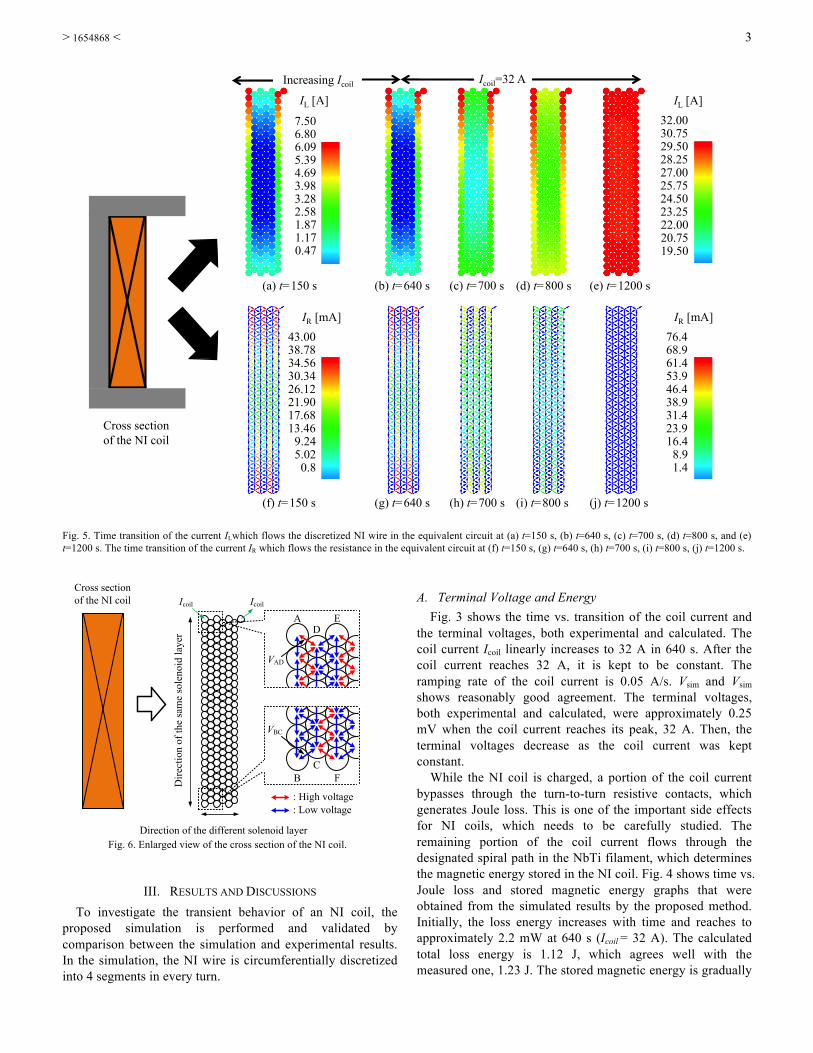
ramping, which are incompatible to each other, need to be compromised. For this purpose, we performed a simulation research to comprehend a non-uniform current path within the NI coil. Fig. 5 shows the temporal variation of the coil current distributions in the NbTi filaments of the NI coil, which were obtained using the proposed equivalent circuit approach. In Figs. 5(a) and (b), while the coil current Icoil increases, most of the current flows in the innermost and outermost layers. After Icoil reaches its peak (32 A), the distribution of the current IL becomes more uniform as shown in Figs. 5(c)-(e). During charging the NI coil (t<640 s), the current in the top of the first inner layer bypasses to the second inner layer. Therefore, IL decreases along the wire (axially downward in Fig. 5) in the first inner layer, i.e., a portion of the current bypasses to the adjacent wire as the current IR. Consequently, the current IL in the center region is small, e.g., 0.47 A at t=150 s as shown in Fig. 5(a). The primary reason for the small current at and near the center region is the induced inverse voltage. Note that the currents flow mostly in the top and bottom of the coil during charging, 0<t<640 s.
Figs. 5(f)-(j) show the distributions of bypass current IR. In Figs. 5(f) and (g), i.e. during charging (t<640 s), the current IR slowly increases as the coil current increases. After the coil current reaches 32 A and is kept constant, the current IR gradually decreases and becomes zero at t=~1200 s.
The bypassing currents, large or small, between the layers on the top and bottom of the NI coil are shown in Fig. 5(f). The reason is that the high voltage between the different layers appears when its distance along the wire is long. The turns A and D in Fig. 6 are connected to each other, while the distance between A and D along the wire is "long". As the result, the voltage VAD is high, and the current IR is large there. On the other hand, the voltage VBC between the turns B and C is very small since the distance along the wire is very short. Consequently, the currents of A-D and C-F are much larger than those of B-C and D-E.
From the above investigations, there are mainly two current paths between the terminals. One is the path completely along the NbTi filament of the wire and the other is the bypass on the top and bottom of the NI coil. The coil current flowing along the NbTi filament generates the magnetic energy, while the other one flowing in the resistive path is attenuated with generating the Joule loss. In view point of improvement of decreasing the loss energy and shortening the charging time, the partial insulation may be effective [7]. To investigate this issue, further researches are required.
IV. CONCLUSION The no-insulation (NI) technique may be useful for low
temperature superconducting (LTS) magnet applications since it may be effective to improve the dynamic stability of an LTS coil. We investigated a numerical approach to estimate the transient behavior of an NI coil. In order to identify the loss energy of an NI coil during charging, an equivalent circuit model is proposed with the inductance of the discretized NI wire and the contact resistance between the adjacent wires taken into consideration.
The terminal voltage and the energy of the NI coil are computed by solving the equivalent circuit equations based on the Kirchhoff’s laws. The simulation results agreed well with the experimental ones. Additionally, the non-linear current path within the NI winding is also investigated numerically. In simulation, the coil current is assumed to flow in two paths between the terminals. One is along the superconducting filament of the NI wire, and the other in the resistive path of the contacting wires. The former is associated with the stored magnetic energy, and the latter is attenuated with the loss energy.
In future, the proposed circuit analysis method is coupled with a thermal analysis. The dynamic stability for a heat has to be investigated by the analysis method considering the thermal behavior.
REFERENCES [1] S. Hahn, D. K. Park, J. Bascuñán, and Y. Iwasa, “HTS pancake coils
without turn-to-turn insulation,” IEEE Trans. Appl. Supercond., vol. 21, no. 3, pp. 1592-1595, 2011.
[2] S. Hahn, D. K. Park, K. Kim, J. Bascuñán, and Y. Iwasa, “No-Insulation (NI) winding technique for premature-quench-free NbTi MRI magnet,” IEEE Trans. Appl. Supercond., vol. 22, no. 3, p. 4501004, 2012.
[3] S. Choi, H. C. Jo, Y. J. Hwang, S. Hahn, and T. K. Ko, “A study on the no insulation winding method of the HTS coil,” IEEE Trans. Appl. Supercond., vol. 22, no. 3, p. 4904004, 2012.
[4] S. Hahn, D. K. Park, J. Voccio, J. Bascuñán, and Y. Iwasa, “No-Insulation (NI) HTS inserts for > 1 GHz LTS/HTS NMR magnets,” IEEE Trans. Appl. Supercond., vol. 22, no. 3, p. 4302405, 2012.
[5] Y. Kim, S. Hahn, K. L. Kim, O. H. Kwon, H. Lee, “Investigation of HTS racetrack coil without turn-to-turn insulation for superconducting rotating machines,” IEEE Trans. Appl. Supercond., vol. 22, no. 3, p. 5200604, 2012.
[6] H. Shin, K. L. Kim, Y. H. Choi, O. J. Kwon, S. Hahn, Y. Iwasa, H. G. Lee, “Effects of impregnating material on thermal and electrical stabilities of the HTS racetrack pancake coils without turn-to-turn insulation,” IEEE Trans. Appl. Supercond., vol. 23, no. 3, p. 7700404, 2013.
[7] S. Noguchi, Y. Kim, S. Hahn, and Y. Iwasa, “Charging test of Partial-Insulation (PI) winding technique for NbTi MRI magnets,” presented at MT-23, 2013.