Numerical modelling of near field optical data storage - VTT · Numerical modelling of near field...
106
ESPOO 2005 ESPOO 2005 ESPOO 2005 ESPOO 2005 ESPOO 2005 VTT PUBLICATIONS 570 Kari J. Kataja Numerical modelling of near field optical data storage
Transcript of Numerical modelling of near field optical data storage - VTT · Numerical modelling of near field...
VTT PU
BLICATIO
NS 570
Num
erical modelling of near field optical data storage
Kari J. K
ataja
Tätä julkaisua myy Denna publikation säljs av This publication is available from
VTT TIETOPALVELU VTT INFORMATIONSTJÄNST VTT INFORMATION SERVICEPL 2000 PB 2000 P.O.Box 2000
02044 VTT 02044 VTT FI–02044 VTT, FinlandPuh. 020 722 4404 Tel. 020 722 4404 Phone internat. +358 20 722 4404Faksi 020 722 4374 Fax 020 722 4374 Fax +358 20 722 4374
ISBN 951–38–6653–X (soft back ed.) ISBN 951–38–6654–8 (URL: http://www.vtt.fi/inf/pdf/)ISSN 1235–0621 (soft back ed.) ISSN 1455–0849 (URL: http://www.vtt.fi/inf/pdf/)
ESPOO 2005ESPOO 2005ESPOO 2005ESPOO 2005ESPOO 2005 VTT PUBLICATIONS 570
Kari J. Kataja
Numerical modelling of near fieldoptical data storage
In this thesis, two future generation optical data storage techniques arestudied using numerical models. Direct semiconductor laser readout (DSLR)system employs external cavity configuration and super resolution (SR)technique an optically nonlinear material layer at the optical disc forrecording and readout operation. Work with the DSLR system is focused onthe studying and optimisation of the writing performance of the system,while work with the SR system has focused on explaining the physicalphenomena responsible for SR readout and writing performance. Bothtechniques enable the writing and readout of the data marks smaller thanthe resolution limit of the conventional optical pickup head. Using SRtechnique 4x increase in the data density in comparison to DVD disk can beobtained. Because the studied structures are in the order of the wavelength,ray tracing and scalar methods cannot be used to model the system. But, thesolution of Maxwell's vector equations is required in order to study thesestructures. Moreover, analytical solutions usually do not exist for suchcomplex structures, thus the numerical methods have to be used. In thisthesis the main modelling tool has been the Finite Difference Time Domainmethod.


VTT PUBLICATIONS 570
Numerical modelling of near field optical data storage
Kari J. Kataja VTT Electronics
Academic Dissertation to be presented with the assent of the Faculty of Technology, University of Oulu,
for public discussion in the Auditorium YB210, Linnanmaa, on September 8th, 2005, at 12 o�clock noon.

ISBN 951�38�6653�X (soft back ed.) ISSN 1235�0621 (soft back ed.)
ISBN 951�38�6654�8 (URL: http://www.vtt.fi/inf/pdf/) ISSN 1455�0849 (URL: http://www.vtt.fi/inf/pdf/)
Copyright © VTT Technical Research Centre of Finland 2005
JULKAISIJA � UTGIVARE � PUBLISHER
VTT, Vuorimiehentie 5, PL 2000, 02044 VTT puh. vaihde 020 722 111, faksi 020 722 4374
VTT, Bergsmansvägen 5, PB 2000, 02044 VTT tel. växel 020 722 111, fax 020 722 4374
VTT Technical Research Centre of Finland, Vuorimiehentie 5, P.O.Box 2000, FI�02044 VTT, Finland phone internat. +358 20 722 111, fax +358 20 722 4374
VTT Elektroniikka, Kaitoväylä 1, PL 1100, 90571 OULU puh. vaihde 020 722 111, faksi 020 722 2320
VTT Elektronik, Kaitoväylä 1, PB 1100, 90571 ULEÅBORG tel. växel 020 722 111, fax 020 722 2320
VTT Electronics, Kaitoväylä 1, P.O.Box 1100, FI�90571 OULU, Finland phone internat. +358 20 722 111, fax +358 20 722 2320
Technical editing Maini Manninen Valopaino Oy, Helsinki 2005

3
Kataja, Kari J. Numerical modelling of near field optical data storage. Espoo 2005. VTT Publications 570. 102 p. + app. 63 p.
Keywords direct semiconductor laser readout system DSLR, super resolution technique SR,Finite Difference Time Domain method FDTD, numerical methods
Abstract In this thesis, two future generation optical data storage techniques are studied using numerical models. Direct semiconductor laser readout (DSLR) system employs external cavity configuration and super resolution (SR) technique an optically nonlinear material layer at the optical disc for recording and readout operation. Work with the DSLR system is focused on the studying and optimisation of the writing performance of the system, while work with the SR system has focused on explaining the physical phenomena responsible for SR readout and writing performance. Both techniques enable the writing and readout of the data marks smaller than the resolution limit of the conventional optical pickup head. Using SR technique 4x increase in the data density in comparison to DVD disk can be obtained. Because the studied structures are in the order of the wavelength, ray tracing and scalar methods cannot be used to model the system. But, the solution of Maxwell�s vector equations is required in order to study these structures. Moreover, analytical solutions usually do not exist for such complex structures, thus the numerical methods have to be used. In this thesis the main modelling tool has been the Finite Difference Time Domain method.

4
Preface The work presented in this thesis was carried out in the Technical Research Centre of Finland, VTT Electronics and in the University of Arizona, Optical Sciences Center, during the years 2001�2005.
My greatest thanks to Dr. Pentti Karioja and Prof. Dennis Howe who gave me an opportunity to study this interesting research field and their support and guidance during the course of this work. I also would like to thank my supervisors Prof. Harri Kopola, VTT Electronics and Prof. Risto Myllylä, Department of Electrical and Information Engineering at the University of Oulu for their support.
The financial support is also acknowledged. The work was carried out in the research programs Optical Technologies for Wireless Communication (OTECO) and VTT Key Technology Action: Micro and Nanotechnologies (MINARES). In addition, the work was also supported by the funding from the Academy of Finland, Tauno Tönning Foundation and the Foundation of Technology which is greatly acknowledged
Especially I wish to express my gratitude to my colleagues and co-authors Dr. Janne Aikio, Mr. Juuso Olkkonen, Prof. Junji Tominaga, Dr. Takashi Nakano and Mr. Teemu Alajoki for their contribution, support and many discussions during the work. I would also like to thank all the staff and co-workers in VTT Electronics.
Finally, I wish to thank my friends and family not forgetting my son Henry, who have supported and encouraged me in many ways during these years.
Oulu, June 2005
Kari Kataja

5
List of original publications This thesis consists of the following six publications, which will be referred to by their roman number.
I. Aikio, J., Kataja, K., Alajoki, T., Karioja, P. and Howe, D. Extremely short external cavity lasers: The use of wavelength tuning effects in near field sensing. Proceedings of SPIE � The International Society for Optical Engineering, Vol. 4640. 2002. Pp. 235�245.
II. Aikio, J., Kataja, K. and Howe, D. Extremely short external cavity lasers: Direct semiconductor laser readout modeling by using finite difference time domain calculations. Proceedings of SPIE � The International Society for Optical Engineering, Vol. 4595. 2001. Pp. 163�173.
III. Kataja, K., Aikio, J. and Howe, D. Numerical study of near field writing on a Phase Change optical disc. Applied Optics IP. Vol. 41. 2002. Pp. 4181�4187.
IV. Kataja, K., Olkkonen, J., Aikio, J. and Howe, D. Numerical Study of the AgOx Super Resolution Structure. Japanese Journal of Applied Physics. Vol. 43. 2004. Pp. 160�167.
V. Kataja, K., Olkkonen, J., Aikio, J. and Howe, D. Readout Modeling of Super Resolution Disks. Japanese Journal of Applied Physics. Vol. 43. 2004. Pp. 4718�4723.
VI. Kataja, K., Nakano, T., Aikio, J. and Tominaga, J. Readout signal simulation as a function of readout power of the super resolution optical disk. Proceedings of SPIE � The International Society for Optical Engineering, Vol. 5380. 2004. Pp 663�670.
The author of this thesis was responsible for most of the modelling and manuscript preparation work in all of the papers except [I], where the comparison of a numerical model to experimental results is presented. In [II, III] the author was also responsible for developing the numerical models for direct semiconductor readout modelling except the phenomenological laser model,

6
which was developed elsewhere by Dr. Aikio. In papers [IV�VI] the author studied the physical mechanism responsible for the super resolution readout using numerical models which have been developed by the author, except in paper [V] where Mr. Olkkonen performed most of the programming work of the parallel computing 3D finite difference time domain code.

7
Contents
Abstract ................................................................................................................. 3
Preface .................................................................................................................. 4
List of original publications .................................................................................. 5
List of symbols and abbreviations ........................................................................ 9
1. Introduction................................................................................................... 15 1.1 Objectives of the thesis........................................................................ 17 1.2 Contribution of the thesis .................................................................... 18
2. Optical data storage systems......................................................................... 19 2.1 Near field optical data storage ............................................................. 21 2.2 Direct semiconductor laser optical data storage .................................. 23 2.3 Super resolution optical data storage................................................... 25
3. Numerical models and simulation tools........................................................ 28 3.1 Laser model in ESEC system .............................................................. 28
3.1.1 Effective reflectance method................................................... 28 3.1.2 Phenomenological laser model ............................................... 32
3.2 Maxwell�s equations............................................................................ 34 3.3 FDTD algorithm for solving Maxwell�s equations ............................. 37
3.3.1 Material properties .................................................................. 39 3.3.2 Parallel computing .................................................................. 40 3.3.3 Numerical dispersion .............................................................. 41 3.3.4 Numerical stability criteria for the FDTD algorithm .............. 43 3.3.5 Boundary conditions ............................................................... 46 3.3.6 Initial conditions and source function ..................................... 49 3.3.7 Far-field calculation ................................................................ 55 3.3.8 Discussion on the FDTD model .............................................. 56
4. Validation of the models............................................................................... 58 4.1 Experimental results ............................................................................ 58 4.2 Comparison to analytical models ........................................................ 61
4.2.1 Laser front facet reflection ...................................................... 61

8
4.2.2 Mie scattering.......................................................................... 62 4.2.3 Zero order grating ................................................................... 64
5. Results from DSLR and SR simulations....................................................... 66 5.1 Direct semiconductor laser optical data storage .................................. 66
5.1.1 FDTD simulations with gain medium..................................... 67 5.1.2 Simulations with ESEC model................................................ 68 5.1.3 VSAL spot size modulation .................................................... 73
5.2 Super resolution optical data storage................................................... 74 5.2.1 Writing simulations................................................................. 77 5.2.2 Readout simulations ................................................................ 79 5.2.3 Nonlinear readout characteristics ............................................ 82 5.2.4 Quantum and temperature effects ........................................... 86
6. Conclusions................................................................................................... 88
References........................................................................................................... 89
Appendices Papers I�VI
Appendices of this publication are not included in the PDF version. Please order the printed version to get the complete publication (http://www.vtt.fi/inf/pdf/)

9
List of symbols and abbreviations List of symbols
A Angular frequency spectrum of the electric field
B!
Magnetic flux density
c Speed of light
Ca, Cb Updating coefficients for electric and magnetic fields
dmark Mark size
D!
Electric field density
E!
Electric field
0E Electric field amplitude
gE Longitudinal electric field distribution of the waveguide mode
igE , Incident part of electric field distribution of the waveguide mode
rgE , Reflected part of electric field distribution of the waveguide mode
wgmE Waveguide mode profile of the electric field
Ex, Ey, Ez Electric field components
f0 Electric field frequency
g Gain of the active medium
H!
Magnetic field

10
Hx, Hy, Hz Magnetic field components
i Imaginary part
i, j, k Space steps
I Electric current
J!
Electric current density
k Imaginary part of the refractive index
k~ Numerical wave vector
L Laser cavity length
m Longitudinal laser mode
m Polynomial power of the PML layer
M!
Equivalent magnetic current density
Mwg Electric field modulation inside the laser waveguide
M Readout power modulation at the detector
n Time step
nr Real part of the refractive index
n Refractive index
np Population inversion factor
Np Photon density
Nλ Sampling of the calculation grid

11
q Elementary charge
r1 Laser back facet reflectance
reff Laser front facet effective reflectance
RLOSS Laser cavity loss
RNR Non-radiative recombination rate
RSP Spontaneous recombination rates
RST Simulated recombination rate
S Courant stability factor
t Time
t∆ Time increment
vg Group velocity
pv~ Numerical phase velocity
V Active layer volume
w Either x, y or z axis
zyx ∆∆∆ ,, Space increments
ii yx , Real and imaginary parts of the longitudinal electric field distribution gE
α Loss term of the semiconductor laser
Γ Optical confinement factor

12
∆ Space increment when ∆=∆=∆=∆ zyx
rε Relative permittivity
0ε Free-space permittivity
ε Permittivity 0εεε r=
1η Wave impedance
iη Internal quantum efficiency
θ Incident angle
λ Wavelength
rµ Relative permeability
0µ Free-space permeability
µ Permeability 0µµµ r=
σ Electrical conductivity
∗σ Equivalent magnetic loss
ω Angular frequency
List of abbreviations
CD Compact Disc
CD-DA Compact Disc Digital Audio
CD-R Compact Disc Recordable

13
CD-RW Compact Disc ReWritable
CNR Carrier to Noise Ratio
DSLR Direct Semiconductor Laser Readout
DVD Digital Versatile Disc
EC External Cavity
ESEC Extremely Short External Cavity
FDTD Finite Difference Time Domain
LD Laser Diode
LSC Light Scattering Centre
NA Numerical Aperture
ODS Optical Data Storage
OPH Optical Pickup Head
SIL Solid Immersion Lens
SR Super Resolution
TF/SF Total Field / Scattered Field
VSAL Very Small Aperture Laser

14
15
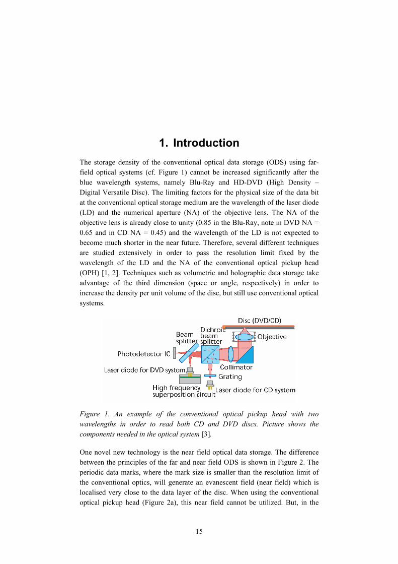
1. Introduction The storage density of the conventional optical data storage (ODS) using far-field optical systems (cf. Figure 1) cannot be increased significantly after the blue wavelength systems, namely Blu-Ray and HD-DVD (High Density � Digital Versatile Disc). The limiting factors for the physical size of the data bit at the conventional optical storage medium are the wavelength of the laser diode (LD) and the numerical aperture (NA) of the objective lens. The NA of the objective lens is already close to unity (0.85 in the Blu-Ray, note in DVD NA = 0.65 and in CD NA = 0.45) and the wavelength of the LD is not expected to become much shorter in the near future. Therefore, several different techniques are studied extensively in order to pass the resolution limit fixed by the wavelength of the LD and the NA of the conventional optical pickup head (OPH) [1, 2]. Techniques such as volumetric and holographic data storage take advantage of the third dimension (space or angle, respectively) in order to increase the density per unit volume of the disc, but still use conventional optical systems.
Figure 1. An example of the conventional optical pickup head with two wavelengths in order to read both CD and DVD discs. Picture shows the components needed in the optical system [3].
One novel new technology is the near field optical data storage. The difference between the principles of the far and near field ODS is shown in Figure 2. The periodic data marks, where the mark size is smaller than the resolution limit of the conventional optics, will generate an evanescent field (near field) which is localised very close to the data layer of the disc. When using the conventional optical pickup head (Figure 2a), this near field cannot be utilized. But, in the

16
near field ODS (Figure 2b) the aperture (or scatterer) which resides in the near field of the data marks will couple the evanescent field to the far field, where a part of this field can be detected and signal will be obtained.
Figure 2. The difference between a) the conventional optical system which cannot separate data marks smaller than resolution limit and b) near field storage where the aperture scatters the evanescent field produced by the small data marks to the far field and readout signal can be obtained.
In this thesis the author has studied the writing and readout characteristics of two different near field ODS systems namely direct semiconductor laser readout (DSLR) and super resolution (SR) systems, which can pass the resolution limit. The modelling work with the direct semiconductor laser readout systems published in the literature has mainly focused on the optimisation of the reflection coefficients from the data marks and laser facets [4, 5]. However, only simple mathematical models for the laser resonator has been used. In addition, the disc has been modelled as a planar surface, with the reflection coefficients fixed at the data marks. In [6] Ukita et al. used the single mode rate equations to describe the laser operation, but still only simple reflection calculations for the effective reflectance has been used. In general, the physical structure of the disc has not been taken into account in the previous work and the vector nature of the electromagnetic fields has been ignored. To our knowledge the analysis of the external cavity (EC) structure in the ODS application which take into account the vector nature of the electromagnetic fields has only been reported in [7].
Most of the publications on the super resolution disc present only experimental results. A few papers have been published considering the analysis of the readout or writing performance of the SR system by simulations [8�10]. On the

17
other hand, some papers have been published where the authors have studied scattering silver (Ag) particle effects [11�13] and movement or displacement of these particles [14] separately without reporting the effects to the readout signal. In addition, some papers have concerned simulation on thermally induced SR with a phase change or semiconductor material layer [15�17]. Even though, in [8�10] an increased signal from the data marks smaller than the resolution limit is reported there has not been a conclusive explanation of what kind of physical mechanism is responsible for the super resolution effect, when the metallic SR layer is used.
1.1 Objectives of the thesis
The main goal of this thesis is to develop the numerical models and modelling tools for studying both the writing and readout performance of the near field optical disc storage systems. Because the studied structures are in the order of the wavelength, ray tracing and scalar methods cannot be used to model these systems. However, the solution of Maxwell�s vector equations are required in order to study these structures. Moreover, analytical solutions usually do not exist for such complex structures, so numerical methods such as finite difference time domain method (FDTD) [18] have to be used. Basic modelling methods and algorithms can be found in the literature and the main task is the implementation of the modelling algorithms to working simulation tools, which can be used to study near field ODS systems.
The motivation for the DSLR system studies has been to understand and study the writing and readout characteristics, when the whole system is taken into account. This work is a continuum to the laser-to-fibre coupling and laser wavelength tuning collaboration research performed at VTT Electronics and Optical Sciences Center in University of Arizona for several years.
On the other hand, the motivation of the SR data storage studies has been to find out the physical phenomena responsible for the SR effect which would enable the optimisation and characterisation of the whole system and explain experimental results. When e.g. antimony (Sb) is used as a SR layer, the phase of the data layer changes from crystal to amorphous at the tip of the readout beam and this introduce the SR effect. However, the overall performance in the

18
experimental work using of Sb layer is not as good as with metallic oxide materials such as AgOx or PtOx. Therefore, these metallic oxide materials are the most promising candidates for future generation ODS system and also the subject for this thesis.
1.2 Contribution of the thesis
The phenomenological laser model used in this thesis is published in [19] and the author�s contribution has been in developing the FDTD modelling tool which can be combined with the laser model. We have compared the experimental results to the numerical model, when using the extremely short external cavity (ESEC) configuration to measure the surface profile of the sinusoidal grating with the laser diode in [I]. In addition, we have verified the performance of the effective reflectance model with an analytical model which confirms that the ESEC modelling works. The FDTD simulations using a gain model which can replace the phenomenological laser model are presented in [II]. In addition, in [II] the simulations using the DSRL system using conventional edge emitting laser or very small aperture laser (VSAL) [20] are presented. In [III] the author has analyzed the effects of the disc�s thin film layer thicknesses to the writing operation and showed results how the cover and insulating layer thicknesses can be used to optimize the absorption at the data layer. In addition, to our knowledge in [II, III] and in [21] it was the first time where the laser spot size modulation at the data layer as a function of the ESEC length was reported.
In the work with the SR system the author presented to our knowledge the first time the simulation using a donut shaped aperture structure in [IV]. In that paper the author analysed the both writing and readout performance of the super resolution disc and showed that the marks smaller than the resolution limit of the conventional optical pickup head can be written and read. In [V] the author extended the readout simulations into 3D space. In addition, in [VI] the author presented the mechanism, which can explain the nonlinear behaviour of the readout signal as a function of the readout power using the donut shaped aperture with the bubble pit structure.

19
2. Optical data storage systems Optical data storage has established a very important role in the everyday lives of modern societies. The status of the ODS in the information network is in two places. At the server end, the ODS is used as a reliable, long-term archival and database storage, and at the user end, as an archive and backup medium for a personal data [1]. In addition, DVD and hard disc recorders have become more common lately and are replacing VHS recorders in home usage. Moreover, in the music, movie, computer game and software resale markets, the optical medium has a monopoly, where all of the products are distributed on CD or DVD.
Figure 1 shows the schematic picture of the conventional optical pickup head, which in this case has two wavelengths for both CD and DVD media. The laser beam is collimated and focused on the data layer of the disc and the reflected light propagates through the same lenses and is focused on the detector in order to obtain the data and the servo signals for focusing and tracking. The achievable storage density of conventional ODS systems is ultimately limited by the diffraction. The conventional OPH is considered a far field optical system [2], where the data is written and read using a conventional diffraction limited optical system and the smallest resolvable mark size is defined by Equation 1 (see, e.g., [22] Chap 5.)
NAdmark 4
λ= , (1)
where λ is the wavelength and NA is the numerical aperture. With DVD specifications (λ = 650 nm and NA = 0.6 [23]) dmark = 271 nm. Note, although Equation 1 sets the limiting size at which the mark no longer modulates the reflected far field light (i.e., it is the resolution limit), serious inter-symbol interference occurs when the marks are separated by distance ~ 1,5 dmark, or less. This is why the minimum mark size in DVD is set at 400nm. The equation shows that as the wavelength is reduced or the NA is increased, smaller marks can be read, which is achieved with a blue wavelength laser and a 0.8 NA lens (Blu-Ray) in comparison with the DVD system. However, the NA of the objective lens can no longer be increased significantly and the shortest

20
wavelength laser diodes currently have a peak wavelength at 375 nm. Therefore, it seems that conventional data storage is reaching its limit in the areal density.
Other data storage media have well-established markets in different fields. For example, magnetic data storage is used in hard disc drives where capacity vs. price and data rate are the most important factors. However, removable floppy disc drives cannot be found in new computers and Compact Flash II-compatible Microdrives (e.g. IBM and Hitachi) are as expensive as Flash memories. One alternative to the floppy disc is the magneto optical medium, however, it is not widely used because of its higher price compared to CD-R (or CD-RW). The reason for the higher price is a more complicated magnetic storage medium and optical pickup head for the polarisation detection of the readout signal than with CD-RW [2]. In recent years, the usage of solid state flash memory has increased mostly due to digital cameras and other portable devices where the small size and weight are the most important factors. However, flash memories are still about 100 times more expensive (�/GB) than hard discs or CD and DVD media and therefore the price limits its usability as an archival storage and software distribution medium. Despite this, USB flash memories will most likely replace floppy discs and also challenge CD-RW in file interchange use, mostly due to robustness, ease of use and the size factor.
Philips and Sony jointly proposed the CD-DA (Compact Disc Digital Audio) format in 1980 after having been separately developing optical storage systems for several years [24]. However, the idea of storing data on the disc and reading it with an optical pickup head is older. Cellitti [25] concluded that the current type of optical medium was first proposed by David Paul Gregg in the 1960s, when he applied for a patent for such a system [25, 26]. After Gregg�s work, the technology was developed in several companies, but failed commercially, even though Laser Disc™ (Pioneer) products have been available in retail stores mainly in Japan.
The original CD-DA standard was designed only for audio applications. Since the original standard (also known as Red Book [27]), several other standards have been proposed. One successful standard has been CD-ROM (Yellow Book [28]), which is used in software distribution. In a little less than 20 years, ODS evolved from CD to DVD, which was introduced in 1997 [23]. Two rival next-generation formats, Blu-Ray and HD-DVD, were introduced in 2002. Blu-Ray

21
offers higher capacity and is backed by the major electronics manufactures, and HD-DVD has better backward compatibility with the DVD standard and has the support of the film studios. Because these standards are not compatible with each other, competition is expected between these standards in the near future [29].
In the progress of storing more data on the disc, the most significant changes have been a shorter wavelength laser diode and a higher NA objective lens [30]. Of course, progress has also been made in the signal processing, error correction and other parts of the drive systems and medium [31]. On the other hand, several different techniques are constantly being studied in order to increase the data density and data rate of ODS. These techniques include, e.g., holographic [32, 33], multi-layer [34] (a double-layer DVD can also be categorised as a multi-layer recording), pit-pattern modulation [35] and near field storage technologies. Furthermore, near field ODS contains several different fields (see, e.g., [2]) such as the near field scanning optical microscope, which can utilize either a solid immersion lens (SIL) [36�39] or a tapered optical fibre tip [40, 41], direct semiconductor laser readout [5, 6, 20, 42�44], planar aperture probe [45, 46] and super resolution (SR) techniques [47�50]. Different near field optical data storage systems are discussed briefly in Section 2.1. The operational principles of the direct semiconductor readout and super resolution techniques that are studied in this thesis are introduced in Sections 2.2 and 2.3.
2.1 Near field optical data storage
Near field ODS techniques rely on the evanescent coupling of light to the data layer of the optical storage medium in order to read and write data marks smaller than the diffraction limit of conventional optics (Equation 1). In the solid immersion lens system, the laser beam is focused on the disc�s data surface with a hemispherical lens that effectively exhibits a numerical aperture > 1 [51]. This is achieved by coupling light that suffers total internal reflection within the SIL across a small air gap that separates the SIL and the storage medium. This requires the SIL to be attached to an air bearing flying slider similar to that which is used in hard disc drives (Figure 3a). A modified system, which has a small conical probe tip (Figure 3b) located on the exit surface of the SIL, can be used to reduce the focused spot size on the storage medium even further [52].

22
Figure 3. Schematic pictures of the a) the SIL lens attached to air bearing flying slider [2] and b) the SIL lens with conical tip [52].
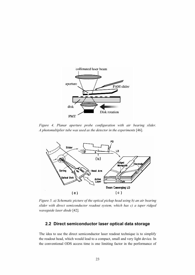
Planar aperture probe (Figure 4) [46] and direct semiconductor laser readout (Figures 5 and 6) techniques take advantage of the small aperture which diameter is less than the wavelength of the laser diode. This aperture is located in the air bearing slider in order to achieve a short distance between the aperture and the disc and therefore evanescent light is coupled to the data layer. In the super resolution technique, the aperture layer is manufactured onto the disc itself, which is an advantage in the sense that the conventional (far-field) OPH can be used instead of a low flying, air bearing slider and the first surface recording optical disc. The flying slider can be a problem because of dust entering the system and the first surface recording medium because of possible scratches on the surface of the disc. The first surface recording optical disc has a very thin cover layer (e.g. 100 nm) at the top of the recording surface in comparison to the SR disc (cf. Figures 7 and 8) which is read through, e.g., 1.2 mm thick substrate (CD medium has 1.2 mm substrate and DVD has 0.6 mm substrate). Because of the thin cover layer, the data layer is vulnerable to the scratches. On the other hand, hard coatings have been studied for the Blu-Ray format, which currently needs a cartridge to cover the surface of the disc [53, 54] in order to reduce the problems in readout due to scratches on the surface of the disc. These kinds of coatings most likely need to be applied to techniques that use the flying slider. In addition, the distance between the aperture (i.e. the SR layer) and the data layer is well controlled in the manufacturing process of the disc. DSLR and SR techniques are discussed in more detail in the next sections.
23
Figure 4. Planar aperture probe configuration with air bearing slider. A photomultiplier tube was used as the detector in the experiments [46].
Figure 5. a) Schematic picture of the optical pickup head using b) an air bearing slider with direct semiconductor readout system, which has c) a taper ridged waveguide laser diode [42].
2.2 Direct semiconductor laser optical data storage
The idea to use the direct semiconductor laser readout technique is to simplify the readout head, which would lead to a compact, small and very light device. In the conventional ODS access time is one limiting factor in the performance of

24
the system. This is because of the relatively large size and the mass of the OPH. In the DSLR technique, the pickup head (laser- and photodiodes) is located at the tip of the flying slider. The slider is similar to that which is used in the hard disc drives and it enables access time relative to hard drives. In addition, using a very small aperture laser, the data density can be increased from conventional optical data storage.
The principle of the DSLR system is shown in Figure 6. The air gap and the first surface recording optical disc form the ESEC at the front facet of the semiconductor laser diode. In the ESEC, part of the light emitted by the laser diode is reflected from the disc and is coupled back into the laser cavity. This coupled light forms an optical feedback loop that affects the LD�s operating wavelength, optical output power and forward bias voltage. Changes in these parameters are used to read the data. The photodiode (PD), which is used to monitor the power and wavelength of the laser, is located close to the back facet of the LD.
Figure 6. Schematic picture of the direct semiconductor laser readout system using a very small aperture laser and the first surface optical disc. Photodiode at the back facet of the laser is used to monitor the laser power. Extremely short external cavity is marked with a dashed line.
Using the external cavity system in optical memory applications was first proposed by Mitsuhashi et al. [55�57]. In 1989, Ukita et al. [42] proposed the

25
OPH, which uses the ESEC configuration for the data readout. After Ukita�s original paper, they published papers concerning performance and reliability [43], temperature control with a diamond coated slider [58] and the optimum laser facet design [6, 59]. In 1993, Goto et al. proposed the EC system using an optical floppy disc [44, 60, 61]. In addition, other research groups have studied the ESEC system theoretically [4, 5, 19] and experimentally with VSAL structure [20] and vertical cavity surface emitting laser arrays [7, 62�67].
2.3 Super resolution optical data storage
The super resolution effect is introduced in an optical storage system whenever there is an optically nonlinear material layer in the disc. This layer can be the recording medium itself or an additional thin film layer which is located near the recording medium [47]. Figure 7 shows schematically the super resolution disc with the aperture formed into the optically nonlinear (super resolution) layer above the data layer. This aperture enables the writing and readout of data marks smaller than the resolution limit of the conventional OPH. The current type of optical super resolution medium was first proposed by Tominaga et al. in [48], where they used Sb medium as a SR layer. Since then, many different material candidates for the SR medium have been studied [14, 48, 49, 50, 68�72]. The most promising media currently being studied are metallic oxide SR thin films. Using these materials, even as small as 50 nm marks are written and read with good a carrier-to-noise (CNR) ratio using the Blu-Ray OPH. This is 8 times smaller than the smallest mark in DVD disc.
When using the metal oxide (e.g. AgOx or PtOx) SR layer, it is deposited in the manufacturing process as an oxide, but during the writing process the metal oxide reduces into metal particles and oxygen. This chemical process is a function of the temperature, which means that if the laser power is chosen properly only the tip of the focused laser spot will have an effect on the SR layer and the small aperture can be formed (cf. Figure 8). In addition, it has been assumed that this process is reversible, which means that after the laser power is switched off the SR layer is transformed back to metal oxide form. This means that during the writing process the aperture is located at the same position where the data marks are written and during the readout the aperture scans the data layer at the same position than the laser beam. This dynamical behaviour has

26
been the original idea of how the aperture is formed in the SR layer. This has also been the starting point for the numerical simulations performed in [IV, V], when the formation of the permanent apertures, which is introduced below, was not published yet.
Figure 7. Schematic of the super resolution system. The conventional optical pickup head is used to write and read the data. A small aperture is formed inside the nonlinear material (super resolution) layer.
Figure 8. Schematic picture of the dynamical behaviour of an SR ODS . The thin film structure is manufactured on a pregrooved disc substrate. During the writing process, the aperture is formed dynamically which means that after the writing process the SR layer will return back to its initial state. During readout, small marks can be read with a dynamic aperture.

27
In the most recent experimental work with the AgOx [73] or PtOx [14] SR layers, it has been observed that the SR layer is permanently damaged during the writing process (Figure 9). In addition, the phase change data layer (either GeSbTe or AgInSbTe) is found to be in a fully crystalline phase [14, 73], that is, there are no amorphous marks in the otherwise crystalline phase data layer. This means that the data marks are formed via the deformation of the thin film layer structure during the writing process. In this process, the oxygen bubbles are formed in the metal oxide SR layer and the metallic particle aggregates are formed inside these bubbles [14, 50, 73]. These bubbles actually form the data marks.
Figure 9. A TEM image of the recorded super resolution disc structure. The thin film structure of the disc is permanently damaged. Oxygen bubbles and particles inside these bubbles are clearly shown. [14]

28
3. Numerical models and simulation tools In this section, the simulation models that have been used in this thesis will be introduced. The laser model, which includes the calculation of the effective reflectance and the phenomenological laser model, is briefly discussed in Section 3.1. A more detailed introduction to the laser model can be found in [74]. Maxwell�s equations are presented in Section 3.2 and the FDTD algorithm that is used to solve them numerically is briefly introduced in Section 3.3 with discussion e.g. about numerical accuracy, boundary conditions and source implementation.
3.1 Laser model in ESEC system
The semiconductor laser diode is the key component when the external cavity systems are being studied. Aikio and Howe [19] have constructed a simple, but sufficiently accurate, model to simulate the ESEC semiconductor laser system that is presented in Section 3.1.2. This model takes the semiconductor laser dynamics into account in the presence of the external feedback. In addition, the diffraction of light in the ESEC, as well as the coupling of light back into the LD�s active region (waveguide), are taken into account using the effective reflectance method [74], which is presented first. In addition, a macroscopic Lorenzian gain model is also used. Details of this model can be found in [18].
3.1.1 Effective reflectance method
The influence of the external cavity is taken into account as a virtual mirror with both phase and amplitude reflectance characteristics. Figure 10 shows, as an example, a simple disc structure that is reduced to a simple reflective mirror with a specific reflectance value depending on the ESEC�s geometry. The numerical simulation of the ESEC structure, which takes into account the disc structure and the small part of the laser diode, is calculated with the FDTD method. In FDTD simulations, the laser structure is modelled as a simple three-layer structure (core and cladding layers), which defines the transversal waveguide mode. In [II, III] a 400 nm long part of the laser waveguide is included in the model in addition to the air gap and optical disc structure. The effective reflectivity model applies

29
when there is no macroscopic time delay in the optical feedback, which could cause severe dynamical effects to the laser operation. In this thesis, it is assumed that the dynamical effects do not affect performance, because it would require the EC length to be in the order of centimetres or more [74].
Figure 10. Principle of the effective reflectance method. The complex structure in front of the laser diode is reduced to an effective (virtual) mirror with complex valued reflection constant.
Figure 11. Electric field amplitude of the solitary laser structure in the FDTD simulation at the steady state situation. Laser structure is at z-axis from 0.0�0.6 µm. Standing wave pattern is located inside the laser.

30
When ESEC systems are modelled, the FDTD simulation is continued until the steady state situation is reached in order to calculate the effective reflectance. Figure 11 shows an example of the electric field amplitude at the steady state situation in the case of a solitary laser diode. The system is described in more detail in Section 4.2.1 and at this point it is only mentioned that inside the laser cavity, a standing wave pattern is formed and reflectivity is calculated from the modulation of this pattern.
Because the transversal shape of the reflected field is not exactly the waveguide mode of the laser diode, the coupling of the reflected field back to the laser cavity is achieved using the overlap integrals over the waveguide mode and the total field obtained from the FDTD model.
( ) ( ) ( )( ) ( )
( )[ ] ( )[ ]0000
,,
*
expexp
,,,
zzikErzzikE
zEzE
dxdyyxEzyxEzE
eff
rgig
wgmtotalg
−+−−=
+=
= ∫, (2)
where Etotal is the total field calculated using the FDTD method, Ewgm is the transverse profile of the guided mode and z0 is the reference plane at the z-axis. Equation 2 shows that the guided part of the field is a coherent sum of the incident (Eg,i) and reflected (Eg,r) waves. For harmonic fields, Eg is a complex valued function, which draws an origin centred ellipse in the complex plane. The lengths of the major and minor axes of this ellipse (i.e. the extreme absolute values of Eg) are
( ) ( ) ( ) ( )tzErtzEtzEE igeffrgigg ,1,, ,,,max, +=+= , (3a)
( ) ( ) ( ) ( )tzErtzEtzEE igeffrgigg ,1,, ,,,min, −=−= , (3b)
where, |Eg,r(z, t)| = |reff||Eg,i(z, t)| has been used. Now, we see that the modulation (Mwg) of |Eg(z, t)| directly gives the amplitude of the electric field reflectance

31
effgg
ggwg r
EE
EEM =
+
−=
min,max,
min,max, . (4)
The phase of the reflectance is determined by the locations of the minima and maxima of Eg. Because numerical errors may occur in the FDTD calculation and the maxima and minima may not be exactly at the calculation grid point, the values of Eg only approximate an ellipse. Therefore, an ellipse is fitted to this data using a pseudo inverse matrix (see e.g. [75]) method to obtain the coefficients for a set of equations
122 =++ iiii cyybxax , (5)
where ( )igi Ex ,Re= and ( )igi Ey ,Im= and a, b and c are the unknown coefficients of the polynomial that defines an ellipse. Eg,i is the value of the overlap integral at grid point i. The matrix representation for Equation 5 is
T1...11=XA , where Tcba=A and
222
21
2211
222
21
...
...
...
n
nn
n
yyyyxyxyx
xxx=X . (6)
Now, the polynomial factors (A) that give the least mean square fit are given by T
321T1...11 ∑∑∑ ++++ ==
jj
jj
jj XXXXA , (7)
where X+ is the pseudo inverse of X. The lengths of the axes of the ellipse are given as the elements of the following diagonal matrix D
( )min,
max,
00
22
g
g
EE
cbba
diagdiag =⎟⎟⎠
⎞⎜⎜⎝
⎛== BD , (8)
where matrix B is chosen in such a way that

32
122T =++= nnnn cyybxaxyxyx B (9)
yields the equation for the ellipse (Equation 5). Diagonalisation of matrix B represents a coordinate transformation to a coordinate system in which the axes of the ellipse lie parallel to the coordinate axes. The values of Eg,max and Eg,min obtained from Equation 8 are inserted into Equation 4 to calculate the effective reflectivity, which is then used in the phenomenological laser model to calculate the output spectrum of the laser. In the next section, the phenomenological laser model is briefly introduced.
3.1.2 Phenomenological laser model
The laser model uses multimode steady state rate equations (see e.g. [76]). The derivation presented here follows paper [19]. The carrier rate equation in the steady state is given by
⎟⎠
⎞⎜⎝
⎛++= ∑
mmSTSPNR
i
RRRVqI ,η, (10)
where I is the electric current, V is the volume of the active layer, q is the elementary charge, ηi is the internal quantum efficiency, RNR, RSP and RST are the non-radiative, spontaneous and stimulated recombination rates, respectively. The summation in Equation (10) is over the longitudinal modes and RST,m is the stimulated recombination rate corresponding to oscillation mode m. The photon rate equation is
mSPmmLOSSmSTm RRR ,,, 'Γ Γ−= , (11)
where Γm is the optical confinement factor, RLOSS,m is the cavity loss rate and mSPR ,' is the modal spontaneous emission for the longitudinal mode m. The
stimulated emission rate is given by
mpmmgmST NgvR ,,, = , (12)

33
where vg,m is the group velocity, gm is the gain of the active medium and Np,m is the photon density. In [II, III] the carrier density dependent gain spectrum was modelled for a bulk material. However, quantum well [74, 77, 78] and measured [74, 79] gain data can be used also. The photon loss rate is obtained from
mpmmgmLOSS NvR ,,, α= , (13)
where imMm ααα += , is the decay term that includes mirror loss imM ,α and
the internal absorption iα . The amplitude of the effective reflectance calculated
using the FDTD simulations is taken into account in the mirror loss term ( ) Lrr meffmmM 2ln ,,1, −=α . In the simulations, reff has to be simulated with at
least two wavelengths and linear interpolation is used to obtain reflectance at the laser wavelengths. The photon density can now be solved from Equations 11�13
( )mmmmg
mSPmp gv
RN
Γ−=
α,
,,
'. (14)
Relation between mSPR ,' and mSTR , is obtained from Einstein�s coefficients
mSTmpmp
mSPmSP R
VNn
R ,,,
,,' = , (15)
where nSP,m is the population inversion factor and Vp,m = V/Γm is the total volume occupied by photons. Using Equation 12, the following equation can now be obtained
Vnvg
R mSPmgmmmSP
,,,'
Γ= . (16)
Inserting Equations 16 and 14 into Equation 12 the following expression is obtained for the stimulated emission rates

34
( ) ( )∆+∆−∆=
Γ−=
mm
mmSPmg
mmm
mmSPmgmST gV
gnvgV
gnvR
αα
2,,
2,,
, , (17)
where ∆αm = αm - αn, ∆gm = Γmgm � Γngn, and ∆ = αn � Γngn. That is, the gain and loss are given relatively to the principal lasing mode n. At the threshold, the stimulated emission rate in Equation 10 is negligible, thus
( ) ( )( )thSPthNRi
th NRNRVqI +=η
. (18)
Above the threshold, quantum conservation is obeyed and
( )∑ ∆+∆−∆+=
m mm
mmSPmg
ith gV
gnvVqIIαη
2,, . (19)
From Equation 19 it is possible to numerically solve ∆ versus current I. The resulting ∆ is inserted into Equation 17 to obtain stimulated emissions rates for individual modes. Finally, the total output spectrum of the laser is obtained from
( ) ( ) ( )∆+∆−∆=∆=∆
mm
mmSPmg
m
mMmmST
m
mMmmout gV
gnvhvRVhvP
ααα
αα 2
,,,,
,, , (20)
where hvm is the photon energy. [19]
3.2 Maxwell�s equations
In order to derive the algorithm for FDTD calculations, we start from Maxwell�s equations. In the source free space, Maxwell�s equations in the differential form are (see e.g. [80])
MEtB !!!
−×−∇=∂∂
, (21)

35
JHtD !!!
−×−∇=∂∂
, (22)
0=⋅∇ D!
, (23)
0=⋅∇ B!
, (24)
where B!
is the magnetic flux density, E!
is the electric field, M!
is the equivalent magnetic current density, D
! is the electric field density, H
! is the
magnetic field and J!
is the electric current density. In addition, in linear, isotropic and non-dispersive material, the following proportions can be written
ED r
!!0εε= , (25)
HB r
!!0µµ= , (26)
where rε is the relative permittivity, 0ε is the free-space permittivity, rµ is the relative permeability and 0µ is the free-space permeability. If the material has electric or magnetic losses, we can write
EJ!!
σ= , (27)
BM!!
∗= σ , (28)
where σ is the electrical conductivity and ∗σ is the equivalent magnetic loss. Now, if equations 25-28 are substituted into equations 21 and 22, we get
( )HEt
H !!!∗−×∇−=
∂∂ σ
µ1
, (29)
( )EHtE !!!
σε
−×∇−=∂∂ 1
, (30)

36
where ε = ε0εr and µ = µ0µr. When curl operators in equations 29 and 30 are written out in Cartesian coordinates, we have a set of six scalar equations that are coupled together
⎟⎟⎠
⎞⎜⎜⎝
⎛−
∂∂
−∂
∂=
∂∂ ∗
xzyx H
yE
zE
tH σ
µ1
, (31a)
⎟⎠⎞
⎜⎝⎛ −
∂∂
−∂∂
=∂
∂ ∗y
xzy Hz
Ex
Et
Hσ
µ1
, (31b)
⎟⎟⎠
⎞⎜⎜⎝
⎛−
∂
∂−
∂∂
=∂∂ ∗
zyxz H
xE
yE
tH σ
µ1
, (31c)
⎟⎟⎠
⎞⎜⎜⎝
⎛−
∂
∂−
∂∂
=∂∂
xyzx E
zH
yH
tE σ
ε1
, (32a)
⎟⎠⎞
⎜⎝⎛ −
∂∂
−∂∂
=∂
∂y
zxy Ex
Hz
Ht
Eσ
ε1
, (32b)
⎟⎟⎠
⎞⎜⎜⎝
⎛−
∂∂
−∂
∂=
∂∂
zxyz E
yH
xH
tE σ
ε1
. (32c)
Partial differential equations (equations 31 and 32) are the core of the FDTD algorithm, where it is not necessary to enforce boundary conditions at the surface of the objects. In addition, Gauss�s Law (equations 23 and 24) does not have to be explicitly defined. A FDTD space grid only has to be constructed in such a way that Gauss�s Law relations are implicit in the positions of E and H field components in the grid and the numerical space-derivation (curl) operations to these field components can be calculated [18, 81].

37
3.3 FDTD algorithm for solving Maxwell�s equations
The FDTD method was introduced by Kane Yee in 1966 [82]. His insight was to solve Maxwell�s differential equations numerically with finite differences in time and space. Yee used the central differences in a staggered space grid and a leapfrog time stepping algorithm in his original paper. Since then, many different gridding and time-stepping algorithms have been presented [83]. However, the original algorithm is still widely used because of its simplicity.
The FDTD algorithm is based on solving Equations 31 and 32 numerically using central differences. Figure 12 shows the Yee unit cell, where every E component is surrounded by four H components and vice versa. This kind of geometry can also be elegantly used to visualise Ampere�s and Faraday�s laws in the integral form. The FDTD algorithm can also be deduced from these integral equations [18, 84].
Figure 12. Position of the electric (black arrows) and magnetic (white arrows) field vector components of the Yee cell.
In the following, we derive the numerical approximation for Equation 32a, where the partial derivates for time and space are written using central differences

38
⎟⎟⎟⎟
⎠
⎞
⎜⎜⎜⎜
⎝
⎛
−
∆
−−
∆
−
=∆
−
++++
++++++
++
−
++
+
++
n
kjixkji
n
kjiy
n
kjiyn
kjizn
kjiz
kji
n
kjixn
kjix
E
z
HH
y
HH
t
EE
21,21,21,21,
,21,1,21,21,,21,1,
21,21,
21
21,21,
21
21,21,
1
σε
. (33)
On the right-hand side, all field components are evaluated at time step n, whereas at the left-hand side, the Ex field has 21+= nt and 21−= nt components. Because Ex is not calculated at time step n, the following approximation is performed in order to eliminate the t = n component
2
21
21,21,
21
21,21,21,21,
−
++
+
++
++
+=
n
kjixn
kjixn
kjix
EEE . (34)
That is, Ex at time step n is just an average of the previous ( 21+= nt ) and future ( 21−= nt ) values of Ex. Now, if we substitute Equation 34 into
Equation 33 and multiply both sides with ∆t and collect 21
21,21,
+
++
n
kjixE terms to
the left-hand side, we obtain
⎟⎟⎟
⎠
⎞
⎜⎜⎜
⎝
⎛
∆
−−
∆
−∆
+⎟⎟⎠
⎞⎜⎜⎝
⎛ ∆−=⎟
⎟⎠
⎞⎜⎜⎝
⎛ ∆+
++++++
++
−
++++
+++
++++
++
z
HH
y
HHt
Et
Et
n
kjiy
n
kjiyn
kjizn
kjiz
kji
n
kjixkji
kjin
kjixkji
kji
,21,1,21,21,,21,1,
21,21,
21
21,21,21,21,
21,21,21
21,21,21,21,
21,21,
21
21
ε
εσ
εσ
. (35)
Finally, both sides are divided by the ( )21,21,21,21, 21 ++++ ∆+ kjikji t εσ term and
the following time stepping relation is obtained for the Ex component

39
⎟⎟⎟
⎠
⎞
⎜⎜⎜
⎝
⎛
∆
−−
∆
−
+=
++++++
++
−
++++
+
++
z
HH
y
HHC
ECEn
kjiy
n
kjiyn
kjizn
kjiz
kjib
n
kjixkjian
kjix
,21,1,21,21,,21,1,21,21,
21
21,21,21,21,
21
21,21,
, (36)
where
1
21,21,
21,21,
21,21,
21,21,21,21, 2
12
1−
++
++
++
++
++ ⎟⎟⎠
⎞⎜⎜⎝
⎛ ∆+⋅⎟
⎟⎠
⎞⎜⎜⎝
⎛ ∆−=
kji
kji
kji
kjikjia
ttC
εσ
εσ
, (37a)
1
21,21,
21,21,
21,21,21,21, 2
1−
++
++
++++ ⎟
⎟⎠
⎞⎜⎜⎝
⎛ ∆+⋅⎟
⎟⎠
⎞⎜⎜⎝
⎛ ∆=
kji
kji
kjikjib
ttCε
σε
, (37b)
define the material properties of the grid points in addition to the time step. Similar expression can be found for the other E and H field components. This simple expression is the kernel of the FDTD calculation and it is easy to implement with a matrix oriented programming tool such as Matlab® as was done in [I�III]. In order to reduce the time needed for the 2D calculations, the kernel of the code was implemented with the C-programming language and was used in the simulations performed in [IV, VI]. The parallel computing 3D FDTD code used in [V] is implemented with C++ and uses MPI libraries [85].
3.3.1 Material properties
Dielectric and absorbing materials can be directly taken into account using equations above. In the case of a dielectric material Ca = 1 (Equation 37a) and the material properties are defined solely by Cb. When the material has absorption, that is, the refractive index has an imaginary part, the permittivity is defined as
( ) ( )220
20 Re knikn rr −=+= εεε , (38)

40
where nr and k are the real and imaginary parts of the refractive index. Conductivity is calculated from [86]
( ) knikn rr 2Im 02
0 ⋅=+= ωεωεσ , (39)
where ω is the angular frequency. If one needs to model metallic materials, where the imaginary part of the refractive index is larger than the real part, the permittivity in Equation 38 will have a negative value. In that case the coefficient Ca > 1 (Equation 37a) and the calculation is no longer stable, because the electric field amplitude will increase exponentially. Therefore, Lorentz or Debye dispersion models have to be implemented in order to model metallic materials. The details in implementing these models can be found in [18, 87], where especially in [87] there are straightforward guidelines for implementing material models into the simulation code. In this thesis, only the Lorentz model has been used.
3.3.2 Parallel computing
Parallel computing hardware has been built at VTT Electronics previously for telecommunications research. Mr. Olkkonen developed the parallel 3D FDTD simulation tool [88] used in [V]. The motivation for a parallel computing environment comes from the simple fact that the memory capacity and speed of a single desktop computer is not enough for the calculation of 3D problems. Figure 13 shows the measured speed compared to the ideal system in the case of a small test problem. In this example, the speed gain using 8 nodes was only about 5. Ideally, 8 nodes should give 8 times faster calculation. The saturation of the speed comes from the small size of the calculation problem. In this case, the time used in the communication between the nodes relative to the calculation time in the nodes increases as the number of nodes is increased. This means that the ideal speed-up is achieved only when the time of the communication between the nodes approaches zero in comparison to the calculation time.

41
Figure 13. The measured simulation speed as the function of the nodes (Processes) of the parallel computing Beowulf cluster running a 3D FDTD simulation compared to the ideal system.
3.3.3 Numerical dispersion
Numerical dispersion in the FDTD algorithm is related to the finite number of grid points, direction relatively to the grid axis and time step used in the model. In general case, where zyx ∆≠∆≠∆ numerical dispersion relation in the 3D FDTD algorithm is defined as
2
222
2sin1
2sin1
2sin1
2sin1
⎥⎦
⎤⎢⎣
⎡⎟⎠⎞
⎜⎝⎛ ∆
∆+
⎥⎦
⎤⎢⎣
⎡⎟⎟⎠
⎞⎜⎜⎝
⎛ ∆
∆+⎥
⎦
⎤⎢⎣
⎡⎟⎠⎞
⎜⎝⎛ ∆
∆=⎥
⎦
⎤⎢⎣
⎡⎟⎠⎞
⎜⎝⎛ ∆
∆
zkz
yky
xkx
ttc
z
yxω
, (40)
where kx, ky and kz are the numerical wave vector components in each direction [18]. Detailed derivation of Equation 40 can be found in [18]. In order to illustrate the numerical dispersion as a function of the propagating angle, Equation 40 is written in 2D and in square coordinates, where ∆=∆=∆ yx .

42
( ) ( )⎟⎟⎠
⎞⎜⎜⎝
⎛ ⋅∆+⎟⎟⎠
⎞⎜⎜⎝
⎛ ⋅∆=⎟⎟
⎠
⎞⎜⎜⎝
⎛2sin~
sin2cos~
sinsin1 2222
φφπ
λ
kkN
SS
, (41)
where S = c∆t/∆ is the Courant stability factor, Nλ = λ/∆ is the sampling of the calculation grid and k~ is the numerical wave number [89]. This equation cannot be solved in closed form for k~ , but can be easily solved numerically. Finally, normalised numerical phase velocity is defined as
kcv p
~2~ π
= . (42)
Figure 14 shows the numerical phase velocity as a function of the propagation angle in a 2D grid. While the phase velocity should be constant and achieve unity across the spatial angle, the figure shows that the FDTD calculation grid actually introduces numerical anisotropy to the system. The range for the numerical anisotropy and maximum numerical error to the nominal phase velocity for 3 different sampling rates are shown. For example, the maximum numerical error when the sampling Nλ = 10 is about 1.3% and the anisotropy error is about 0.9%. Figure 14 also shows that the numerical error is approximately inversely proportional to Nλ
2.
Figure 14. Numerical phase velocity as a function of the propagation angle in a 2D FDTD model using square orthogonal grid.

43
If the sampling of the grid is fine enough, the numerical error can be neglected. However, if the studied systems include resonance structures or a periodic calculation grid, this might cause problems, because the error is cumulative. That is, it increases linearly with the propagation distance. In this thesis, the effect of the numerical dispersion is assumed to be relatively small, because the usual cell size has been from 2 nm � 10 nm which at a 650 nm (sampling Nλ = 325 and Nλ = 65, respectively) wavelength will lead very low numerical phase velocity and anisotropy errors (see Table 1). It is also possible to reduce this error by increasing numerical phase velocity by some scaling factor, when the initial conditions are know, to obtain the normalised numerical phase velocity vp/c = 1.
Table 1. Numerical error estimations with 2 and 20 nm square cells at 650 nm wavelength in the simulations performed in this thesis.
Sampling Error type
65 325
Maximum numerical 0.034% 0.0013%
Anisotropy 0.020% 0.0007%
3.3.4 Numerical stability criteria for the FDTD algorithm
Numerical stability criteria couples the time step to the size of the Yee cell. In practice, one might want to choose the size of the Yee cell ∆ to be as large as possible in order to minimise the size of the calculation grid and the number of calculation operations, but still keep the appropriate sampling of the problem in hand. One guideline could be that a sphere should be sampled at least with a four grid points along its diameter, but at least 10 points / λ which guarantees a numerical error of less than 1% on the phase velocity of the wave. Taflove et al. [18] defines the stability criterion for the 3D FDTD algorithm as
222
1111
zyxc
t
∆+
∆+
∆
≤∆ , (43)

44
which in the case of a square grid will simplify to
331
1111
2222
ccct ∆
=
∆
=
∆+
∆+
∆
≤∆ , (44)
and the Courant stability criterion is
31
=S . (45)
In 2D, the Courant stability criterion can be obtained similarly and is
21
=S . (46)
However, in the numerical simulations performed in this thesis, the time step was shorter than defined in equations 45 and 46, because there have been instability problems in the simulations especially when using the Lorentz dispersion model. In 3D simulations, the condition S = 0.5 was used which is obtained from [90], where the derivation differs from [18] and S = 0.5 is obtained for both 2D and 3D FDTD models. However, in this thesis, S = 0.75 is used in 2D simulations without stability problems.
Table 2. The modelling parameters used in the Gaussian pulse hitting an Ag cylinder.
Parameter Symbol Value
Refractive index of the cylinder n1 0.2731+4.4304i
Wavelength λ 550 nm
Polarisation TE
Diameter of the sphere d 1 µm
Sampling Nλ 27.5 (20 nm)

45
Figure 15. Convergence as a function of the time step. This curve is used to observe stability and monitor the steady state condition.
In the practical simulations the stability and the convergence of the simulation is monitored calculating the amplitude difference over the whole calculation grid between successive time steps. This gives the convergence function
( )∑∑∑ −= +
i j k
nkji
Nnkjidiff EEA ,,,, , (47)
where N is an integer. Figure 15 shows an example of simulation monitoring in the case of a 2D simulation, where the Gaussian-shaped planewave pulse hits a silver cylinder (see Figure 16). Simulation parameters are shown in Table 2. The characteristic shape of the convergence curve in Figure 15 shows (1) the start of the simulation n < 300, (2) interaction with the structure 300 < n < 1200 and (3) the pulse and scattered field disappear from the calculation grid n > 1500. After that there is another relaxation of the function between 2000 and 2500 time steps, which arises after the first spurious reflections from the boundaries disappear from the grid. This is usually not seen when a continuous source is used in the simulation and steady state situation is studied. Finally, slow convergence as a function of time is observed after time step 2500 in Figure 15.

46
Figure 16. Electric field amplitude of the planewave pulse in a vacuum (travelling from left to right) hitting an Ag cylinder. The simulation is shown at two time steps. Grid size is 500 x 500 cells. The source is defined using the total field / scattered field technique (see Section 3.6.6).
A similar shaped curve to that in Figure 15 is also obtained, if the simulation is calculated to the steady state situation. In that case, the initial drop between n = 1000 and n = 1500 time steps comes from the fact that the leading edge of the source is transmitted and (or) reflected outside the calculation grid. Depending on the system, the convergence after this initial drop will be faster or slower and the calculation is stopped after some amount of time steps. The number of time steps is always tested with one test run in order to obtain the smallest number of time steps required to have a good enough steady-state in a specific geometry. The convergence curve is not used to stop the simulations automatically.
3.3.5 Boundary conditions
In addition to the update equations shown in Section 3.3, it is necessary to consider boundary conditions [18, 91�96] for the calculation grid in order to extend the calculation grid to infinity and thus prevent non-physical reflections from the grid boundaries. If Equation 36 is written for the outermost ( 21,21, ++ kJi grid point at the y-axis) electric field Ex component at the time step 21+n the following is obtained

47
⎟⎟⎟
⎠
⎞
⎜⎜⎜
⎝
⎛
∆
+−
∆
−
+=
++++
++
−
++++
+
++
z
HH
y
HC
ECEn
kJiy
n
kJiyn
kJiz
kJib
n
kJixkJian
kJix
,21,1,21,21,,21,21,
21
21,21,21,21,
21
21,21,
0 . (48)
The magnetic field component at grid position 21,1, ++ kJi does not exist and therefore it is set to zero. This means that the grid boundary is effectively a perfect electric conductor surface, which reflects all of the incident waves. On the other hand, material boundaries inside the calculation grid do not need any special consideration, because they are intrinsically taken into account by the FDTD algorithm. For the grid boundaries, the 2D FDTD code used in this thesis used the original Berenger perfect matched layer (PML) [93] and uniaxial PML (UPML) [18] is used in the 3D FDTD code. The details of these methods can be found in the literature and only the main ideas are presented here.
In the PML (and UPML) method, a region at the boundary of the calculation grid is reserved for a material which ideally will absorb the incident energy before it is reflected from the perfect electric conductor surface and returned back to the calculation space. Both methods take advantage of an anisotropic material that absorbs the incident wave propagating into the material and, more importantly, does not reflect at the material surface. This is achieved by setting the wave impedance equal at both sides of the surface.
PMLPML
PML ηεµ
εµ
η ===1
11 , (49)
where µi and εi are the permeability and permittivity at both sides of the PML boundary. Even though the PML surface boundary does not reflect any power, the PML absorbs only the component that is travelling perpendicular to the surface of the PML. Thus, when the incident angle increases, the reflection also increases. The reflection as a function of the incident angle for both PML and UPML materials can be calculated from Equation 50 in the case of the polynomial conductivity profile.

48
( ) ( )⎟⎠⎞
⎜⎝⎛
+−=
1cos2exp max
mdR θησ
θ , (50)
where η is the impedance and d is the thickness of the PML. In addition, m is the power of the polynomial absorption profile
( ) maxσσm
dww ⎟⎠⎞
⎜⎝⎛= , (51)
where w is the distance in the direction perpendicular to the PML surface (x, y or z). The maximum conductivity is obtained from
( ) ( )( )d
Rmη
σ2
0ln1max
+−= , (52)
where R(0) is the desired minimum reflection.
Figure 17. Reflection of the planewave from the perfect matched layer (PML) as a function of the incident angle with 100 nm (10 cell) thick layer and m = 3.
Figure 17 shows the reflection of the PML layer as a function of the incident angle in air (n = 1) calculated from Equation 50. Now, the thickness of the PML is d = 100 nm, power m = 3 and R(0) = 10-7. As was mentioned previously, the

49
reflection increases as a function of the incident angle and reaches unity when the angle is 90°. However, this is not a huge problem because at large angles the reflected wave will most likely hit the other boundary of the calculation grid at a small angle and is then absorbed (cf. Figure 18).
In order to have lower reflectance at angles close to 90°, one might suggest using a larger value of σmax or polynomial power m. However, due to discretisation and numerical errors, the reflection will eventually start to increase even though σmax is increased and therefore there is the optimal choice for these parameters [18, 97]. In this thesis, the thickness of the boundary has been 8�10 cell points and the power of the polynomial m = 2�3. In addition, the desired reflectance R(0) = 10-7 which is about the optimal choice reported in [97].
Figure 18. Schematic picture of PML layer performance. If the incident angle θ is large, the wave is reflected from the perfect electric conductor, but is absorbed into the PML at the other boundary of the calculation matrix.
3.3.6 Initial conditions and source function
The goal of the initial conditions in FDTD simulations is to realise an accurate electromagnetic source model for the system using as small number of E and H field components as possible. The simplest source is a point source where only one E field component oscillates with the time function
( )tnfEE niz s
∆= 00 2sin| π , (53)
where E0 is the amplitude of the field and f0 is the frequency. If both the amplitude and the phase are needed, as in the case of ESEC modelling, one needs to calculate the complex field. In that case, the source is defined as
50
( ) ( )[ ]tnfitnfEE niz s
∆+∆= 000 2cos2sin| ππ . (54)
The FDTD algorithm does not need to be modified in order to calculate the complex source function. If there is a shortage of memory, it is possible to perform two separate simulations one with the sine and one with the cosine time function and obtain the final results from these separate results. However, it is possible to reduce the calculation time by a factor of two, if steady-state situations are calculated. A simple relation between sine and cosine functions is used
( ) ⎟⎠⎞
⎜⎝⎛ −=
2cossin πxx . (55)
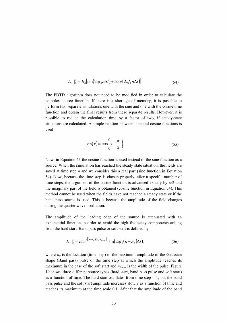
Now, in Equation 53 the cosine function is used instead of the sine function as a source. When the simulation has reached the steady state situation, the fields are saved at time step n and we consider this a real part (sine function in Equation 54). Now, because the time step is chosen properly, after a specific number of time steps, the argument of the cosine function is advanced exactly by π/2 and the imaginary part of the field is obtained (cosine function in Equation 54). This method cannot be used when the fields have not reached a steady state or if the band pass source is used. This is because the amplitude of the field changes during the quarter wave oscillation.
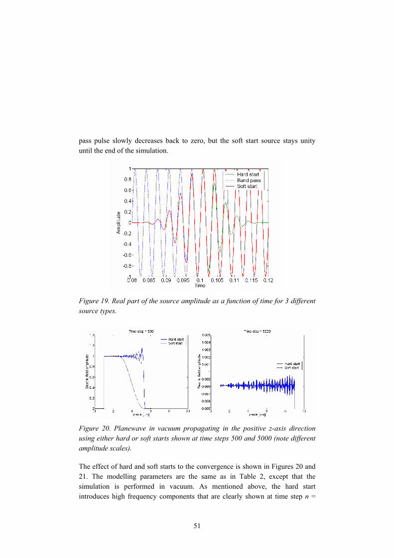
The amplitude of the leading edge of the source is attenuated with an exponential function in order to avoid the high frequency components arising from the hard start. Band pass pulse or soft start is defined by
( )[ ] ( )( )tnnfeEE decay
s
ntnnniz ∆−= ∆−−
000 2sin|2
0 π , (56)
where n0 is the location (time step) of the maximum amplitude of the Gaussian shape (Band pass) pulse or the time step at which the amplitude reaches its maximum in the case of the soft start and ndecay is the width of the pulse. Figure 19 shows three different source types (hard start, band pass pulse and soft start) as a function of time. The hard start oscillates from time step = 1, but the band pass pulse and the soft start amplitude increases slowly as a function of time and reaches its maximum at the time scale 0.1. After that the amplitude of the band
51
pass pulse slowly decreases back to zero, but the soft start source stays unity until the end of the simulation.
Figure 19. Real part of the source amplitude as a function of time for 3 different source types.
Figure 20. Planewave in vacuum propagating in the positive z-axis direction using either hard or soft starts shown at time steps 500 and 5000 (note different amplitude scales).
The effect of hard and soft starts to the convergence is shown in Figures 20 and 21. The modelling parameters are the same as in Table 2, except that the simulation is performed in vacuum. As mentioned above, the hard start introduces high frequency components that are clearly shown at time step n =

52
500 at the leading edge of the source. These might cause stability problems if the sampling is not dense enough. In addition, high frequency oscillation vanishes slowly from the system and therefore the convergence is slow. This is seen in Figure 20 at time step n = 5000 where high frequency oscillation still exists and also in Figure 21, which shows that even after 5000 time steps, the amplitude difference is about 4 orders of magnitude higher with a hard start than with a soft start. This means that even though a soft source requires slightly more time steps to reach a constant amplitude, it is possible to significantly reduce the total number of time steps (and the simulation time) in order to reach the steady state. Therefore, in all of the simulations performed in this thesis, the soft start has been used where typically ndecay = 3⋅10-15 s, which is a few oscillations at visible wavelengths (cf. Figure 19).
Figure 21. Convergence of the FDTD simulation as a function of time step in the case of hard and soft starts.
In addition to the source amplitude as a function of time, it is necessary to implement different amplitude profiles in space coordinates (x, y, z) such as planewave, waveguide modes and Gaussian profile. The analytical waveguide mode which is used in [I�III] is taken from [76] and the Gaussian beam used in [IV�VI] from [98]. In addition, the sources used in this thesis are implemented using the total field / scattered field (TF/SF) technique which implements a non-physical and, more importantly, transparent source plane. The TF/SF technique is based on the linearity of the Maxwell�s equations and is briefly introduced in

53
the following. The detail derivation can be found in the literature [18]. E and H fields at any spatial point can be written thus
scatteredincidenttotal EEE += , (57a)
scatteredincidenttotal HHH += , (57b)
where the total field is separated for the incident and scattered field at any point in the space.
Figure 22. a) Schematic picture the total field / scattered field technique and b) field points at the connecting surface [18].

54
Figure 22a illustrates the technique for the planewave source. The calculation grid is separated into two regions where the total field is calculated in Region 1 and in Region 2 only the scattered field is calculated. A virtual non-physical surface between the total field and scattered field regions is formed which encloses the studied structure. The simulation has a normal PML boundary for lattice truncation. Figure 16 shows an example where a planewave with a Gaussian shaped pulse propagates from left to right inside Region 1 and the scattered field propagates throughout the whole calculation grid. In the case of waveguide or Gaussian shaped amplitude profiles, TF/SF surface is defined only at the one plane (x, y, z0) of the calculation grid. This is enough when the amplitude at the edge of the source plane is negligible. Otherwise, diffraction from the virtual aperture which is formed by the edge of the source plane will affect the simulation.
The FDTD simulation algorithm does not need to be changed in order to implement the TF/SF technique. The source is defined only at the connecting surface and the electric field and magnetic field updates are defined as (see physical location of the grid points in Figure 22b)
⎟⎠⎞⎜
⎝⎛ ⎟
⎠⎞⎜
⎝⎛ +−
∆∆
+=
+
−
+
−
+
+
+
|||
||21
21,
21
21,
21
21,0
,
1
,
n
iincidenty
n
iscatteredy
n
itotaly
n
itotalz
n
itotalz
LLL
LL
HHHx
t
EE
ε
, (58)
⎟⎠⎞⎜
⎝⎛ −⎟
⎠⎞⎜
⎝⎛ −
∆∆
+=
−
−
−
+
−
|||
||
1,,,0
21
21,
21
21,
n
iscatteredz
n
iincidentz
n
itotalz
n
iscatteredy
n
iscatteredy
LLL
LL
EEEx
t
HH
µ
, (59)
where Ex,total update in Equation 58 does not initially have the total field Hy at the point iL - ½. Therefore, the incident field component Hy,incident is added as the source component during the simulation. On the other hand Hy,scattered (Equation 59) has Ez,total at the right hand side from which Ey,incident has to be subtracted during the simulation. Similar adding and subtracting is performed on each side of the connecting surface. Reference [18] presents how the field components are calculated efficiently in the physical locations of 2D or 3D grids.

55
3.3.7 Far-field calculation
In SR simulations, far-field has to be calculated from FDTD simulations in order to model the readout operation. In the simulations performed in [IV�VI], the electric field distribution at the objective lens or at the detector was not of concern, only the total power needed to be calculated. Therefore, simple angular spectrum calculation using Fourier transform is adequate [99]. The angular spectrum of the field component Ew is defined as
( ) ( ) ( )[ ]∫ ∫∞
∞−
+−= dxdyyaxiyxEA ww βπβα 2exp,, , (60)
where Ew is the transversal electric field component (if propagation axis is z then Ex and Ey components). The far-field is calculated separately for each transversal electric field component and the total power is obtained by summation. The power falling to the detector is obtained by integration over the NA of the objective lens
( )[ ]∫∫∑=NA w
w ddAP βαβα 2, , (61)
where it is assumed that all power collected by the objective lens will also reach the detector. In reality this is not the case because of reflection losses at the lens surfaces and beam splitters, in addition to the aberrations and diffraction of the optical system. However, this is not of concern, because at the moment we are not interested about the absolute power level, only about the relative values in order to calculate the signal modulation, which is defined as
minmax
minmax
PPPPM
+−
= , (62)
where P is the power at the detector from Equation 61 and the minimum and maximum are assumed to correspond to on-mark and off-marks situations. In the simulations, it is assumed that the amorphous marks have low reflectivity in comparison to an initially crystalline background. Figure 23 shows the readout power at the on-mark and off-mark situations and the corresponding modulation.

56
Finally, it is noted that the readout carrier-to-noise ratio is related to the square of signal modulation ( 2MCNR ∝ ) [100].
Figure 23. The reflected power at on-mark and off-mark situations and a modulation calculated from those powers. The simulation system is the conventional type DVD disc with 50% duty cycle [V].
3.3.8 Discussion on the FDTD model
In comparison with other numerical calculation methods, such as the Finite Element (see e.g. [101]) or Finite Difference Frequency Domain [81, 102] methods, FDTD has the advantage that it does not need a memory consuming calculation of the linear algebra and inverse matrix. However, the drawback is that in order to obtain a steady state solution, it is necessary to sometimes calculate a relatively large number of time steps that can be a limiting factor when performing calculations. On the other hand, if the response to the electromagnetic pulse is required, FDTD is the method of choice.
When the FDTD method is used, the surface plasmons do not have to be especially considered, but they are intrinsically taken into account. In some

57
cases, a staircase approximation of the object can lead to inaccurate solutions, but e.g. a Mie scattering calculation needs relatively few cells to model the cylindrical or spherical particle in order to obtain a good match between the numerical and analytical methods, even in the near field of the particle surface. Alternative gridding methods, such as non-orthogonal and unstructured grids [18], which can model surface topology more accurately than the original cubic unit cell exist, but they can lead to stability problems and are more difficult to implement.

58
4. Validation of the models The FDTD method itself is known to give accurate results for a wide variety of problems. We have verified the performance of our FDTD codes by comparing them to analytical models and experimental work and the results have been consistent. The comparison of the experimental results from the wavelength tuning of the laser diode to the FDTD simulations are presented in Section 4.1. In addition, the comparisons of the FDTD algorithm to 3 different analytical models are presented in Section 4.2.
4.1 Experimental results
In [I] the FDTD simulations were compared to the measurement results obtained by scanning the laser diode across the surface of the sinusoidal grating surface (see Figure 24) in a direction perpendicular to the grating lines. The LD is brought close to the grating surface (air gap ~5µm) when the light is coupled back to the laser cavity and the laser wavelength is tuned. The laser was moved with a nanopositioning system and the wavelength of the LD was monitored using a spectrum analyzer.
Figure 24. Grating profile measurement setup using ESEC configuration. The laser diode is scanned across the grating and the spectrum analyser is used to monitor the wavelength.

59
When the wavelength data as a function of the scan direction is plotted, it shows that the principal wavelength is tuned periodically as shown schematically in Figure 25. The details for this behaviour can be found e.g. from [74] and here it is only mentioned that every 2π modulation (which corresponds to λ/2 distance in the EC) tunes the wavelength of the laser diode between 790�800 nm. At the nominal wavelength of the LD one 2π tuning period in the measurement corresponds to 795 nm/2 = 397.5 nm distance in the EC.
Figure 25. Schematic picture of the measured wavelength data. Measured wavelength data has 2π modulation as a function of the EC length. Measured profile can be easily visualised by staking the data and extracting the continuous profile from that picture.
When the grating period in the measurement was 30 µm, the results from the surface scanning and numerical simulations agreed well with each other. Figure 26 shows the measured wavelength data, which is transformed to the phase of the external reflection (cf. Figure 25). The FDTD results using a shorter grating period, because of the computational resources, are shown in Figure 27. In addition, the laser performance was not modelled in this work, but the phase was monitored at the front facet of the laser waveguide. Despite this, the figures show a similar structure between the simulations and the experimental data. In addition, the measured wavelength tuning data agrees with the measurement

60
performed with white light interferometer [I]. A particularly interesting feature of the figures is that they both have a similar step structure at the valley of the grating e.g. at a position of 20 µm in Figure 26 and a position of 15 µm in Figure 27, which comes from the tuning periods of the wavelength. This step structure occurs in the discontinuation points where the wavelength jumps from 790 nm to 800 nm (or vice versa, cf. Figure 25).
Figure 26. Measured lasing spectrum of the laser as a function of the scanning position transformed to the phase of the external reflection (+ multiples of 2π) [I].
Figure 27. Simulated phase on the laser facet (+ multiples of 2π) as a function of the scanning position [I].
When the 5 µm period grating was used in the experiments, the actual surface profile was not obtained. The reflected phase at the surface of the laser facet does not follow the grating structure, but has a complicated structure. However, the experimental and modelled data are still in agreement with each other. Similar structures in the phase profile are shown in both phase profiles (see Figures 9 and 11b in [I]).

61
4.2 Comparison to analytical models
4.2.1 Laser front facet reflection
Semiconductor laser diode facet reflectivity has been an interesting problem for laser manufactures, because it affects the transversal mode and the polarisation in addition to the threshold current via the external loss of the laser resonator [103, 104]. In this section, numerical results using the 2D FDTD simulations and effective reflectance calculations are compared to the analytical model [74, 103]. The geometry of the 2D problem is shown in Figure 28 and model parameters are presented in Table 3. The laser is a simple 3-layer structure with the core and cladding layers. The front facet is located in air (n = 1). The core thickness of the waveguide, the refractive index of the cladding material and the polarisation of the source were varied in the FDTD simulation. The reflectance calculation was performed using the effective reflectance technique described in Section 3.1.1.
Figure 28. Laser front facet problem geometry. The refractive index of the cladding (n2) is either 3.24 or 3.492 and the core thickness is varied.
Table 3. The modelling parameters used in the laser front facet reflectivity test.
Parameter Symbol Value
Refractive index of the core n1 3.6
Refractive index of the cladding n2 3.24 or 3.492
Wavelength λ 860 nm
Polarisation TM and TE
Sampling Nλ 172 (5 nm)

62
Figure 29. Laser facet reflectivity in the case TE and TM polarisations with 3% or 10% core to cladding refractive index difference as a function of the core thickness Lcore. The line is analytical and the circles are numerical FDTD solution.
In Figure 29 the calculated reflectivity is compared to the results given in [104]. The reflectivity of the fundamental mode is presented for the TM (Ex, Ey, Hz) and TE (Ez, Hx, Hy) polarisations. Two pairs of curves are calculated for two cladding material refractive indices n2 = 3.24 and n2 = 3.492 corresponding to the index differences of 3% and 10% between the cladding and the core materials. The index of the core is n1 = 3.6 as shown in Figure 28. The results from the FDTD simulations (circles) are in good agreement with the analytical results (lines). In general, the FDTD simulations give slightly higher reflectivity values than the analytical model, where the biggest difference occurs with TM polarisation and a 10% refractive index difference at 300 nm core thickness. These differences arise from numerical errors in the FDTD calculation (sampling, finite calculation grid and absorbing boundary conditions).
4.2.2 Mie scattering
Mie scattering is a classical example of a system where the rigorous analytical solution for Maxwell�s equations can be found (see e.g. [86]). In this example

63
the numerical calculations were performed with the parallel 3D FDTD code. Model parameters are shown in Table 4. Sphere (diameter 1 µm) with an absorbing material is located in air and a planewave is propagating in a positive z-axis direction. The electric field polarisation is along the y-axis. Figure 30 shows the electric field intensity along the propagation direction. The line shows the analytical results while the points are from the numerical solution. The numerical results fit nicely to the analytical curve also with the small structure seen at the 0.5 µm mark.
Figure 30. Electric field intensity calculated analytically or numerically with an FDTD modelling tool. The intensity is plotted along the z-axis which is also the propagation direction of the incident planewave. The 1 µm diameter sphere is centred at zero point in longitudinal dimension.
Table 4. The modelling parameters used in the Mie scattering test.
Parameter Symbol Value
Refractive index n 3.0+1.5i
Wavelength λ 850 nm
Polarisation Ey
Diameter of the sphere d 1 µm
Sampling Nλ 30 (28.3 nm)
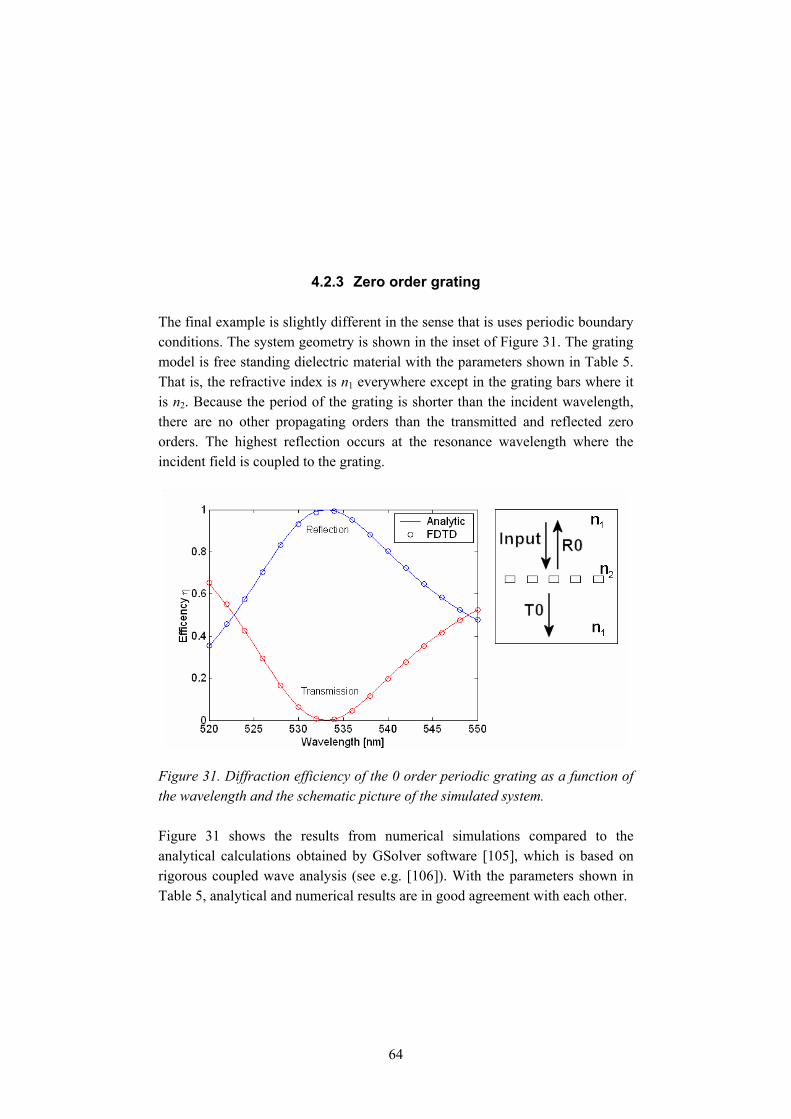
64
4.2.3 Zero order grating
The final example is slightly different in the sense that is uses periodic boundary conditions. The system geometry is shown in the inset of Figure 31. The grating model is free standing dielectric material with the parameters shown in Table 5. That is, the refractive index is n1 everywhere except in the grating bars where it is n2. Because the period of the grating is shorter than the incident wavelength, there are no other propagating orders than the transmitted and reflected zero orders. The highest reflection occurs at the resonance wavelength where the incident field is coupled to the grating.
Figure 31. Diffraction efficiency of the 0 order periodic grating as a function of the wavelength and the schematic picture of the simulated system.
Figure 31 shows the results from numerical simulations compared to the analytical calculations obtained by GSolver software [105], which is based on rigorous coupled wave analysis (see e.g. [106]). With the parameters shown in Table 5, analytical and numerical results are in good agreement with each other.

65
Table 5. The modelling parameters used in the zero order grating test.
Parameter Symbol Value
Refractive index n1 1.0
Refractive index n2 1.5
Period d 500 nm
Height h 150 nm
Duty cycle 0.5
Wavelength λ 520�550 nm
Sampling Nλ ~ 267.5 (2 nm)
Figure 32 shows the electric field amplitude within the grating structure at wavelengths 520 nm and 534 nm where the latter is close to the resonance wavelength. At the resonance wavelength, the transmission is zero, however, there still exists an evanescent field behind the grating which is visualised in Figure 32. It is also noticed that the calculation grid has to be big enough so that the evanescent fields do not touch the PML layer.
Figure 32. Electric field amplitude at the grating when the wavelength is a) 520 nm and b) 534 nm. Four grating lines are shown as faint rectangles.

66
5. Results from DSLR and SR simulations This thesis focuses on the numerical modelling of the two different near field optical data storage techniques. In Section 5.1, the results using the direct semiconductor laser readout system are presented. Section 5.1.1 presents the results obtained by the FDTD model, which uses a gain medium. This model could be used to take the whole system into account using the FDTD simulations and the phenomenological laser model is not needed. The simulations with the phenomenological laser model and FDTD simulations are discussed in Section 5.1.2, where optimisation of the disc structure and effects of the flying height of the laser diode to the performance are discussed.
The simulation results using the super resolution structure are presented in Section 5.2. Results from the writing simulations are presented in Section 5.2.1 where they are compared to the experimental results published earlier. Readout simulations, using different aperture structures are presented in Sections 5.2.2 and 5.2.3 with qualitative comparison to experimental results. Finally, there is a discussion about the quantum effects of the small particles and temperature effects in Section 5.2.4.
5.1 Direct semiconductor laser optical data storage
Preliminary results from the simulations using the ESEC configuration are presented in [II]. It was shown how the ESEC system, including the laser diode, can be modelled using only FDTD simulations, instead of using the separate laser model and FDTD simulations. The laser gain can be modelled using a macroscopic Lorentzian gain profile [107], which does not take account of the atomic-level phenomena and photon-material interactions. The parameters of the Loretzian gain profile are fitted in order to obtain the desired gain characteristics and gain dependent dispersion. In addition, in [II] the laser operation and electromagnetic fields within the ESEC and the laser were modelled using 2D FDTD simulations where the LD was taken into account with an effective reflectance calculation and the phenomenological laser model.
The analysis of the disc parameters of the first surface recording disc to the laser power and the wavelength is presented in [III]. The paper is focused on the spot

67
size at the data layer and the writing characteristics of the system. The readout performance can be analysed using the same model. In addition, in [21] the author has studied the effect of the flying height of the VSAL to the spot size on the data layer.
5.1.1 FDTD simulations with gain medium
Extremely short external cavity systems can be modelled without a separate laser model if the laser gain medium is included in the FDTD model. This can be achieved e.g. using the macroscopic Lorentzian gain model [107]. The FDTD model is the same as presented in Section 3, but the core region has a gain that depends on the electric field amplitude. Figure 33 shows the unsaturated Lorenzian gain profile used in the FDTD model fitted to the gain profile of the GaAsSb � material used in the phenomenological laser model. When using this model, the source is implemented as a random current source inside the laser cavity in each time iteration. When the system has reached a steady state, both the amplitude and the wavelength are fixed by the external cavity structure (including laser) and the gain model. If the ESEC geometry is changed, the laser is tuned accordingly.
Figure 33. Unsaturated GaAsSb and Lorentzian model gain in addition to the loss plotted as a function of wavelength. Vertical lines corresponds to the longitudinal laser modes [II].

68
In Figure 34, an amplitude and wavelength tuning as a function of the air gap from the 1D ESEC model is presented. Due to the 1D model, there is no diffraction of the field outside the laser and therefore the loss is constant as a function of the ESEC length. For the same reason, the peak amplitude of the output power as a function of the ESEC length is also constant (Figure 34a). In addition, the wavelength modulation does not change as a function of the ESEC length (Figure 34b). In 2D and 3D space, the modulation of both of these parameters (power and wavelength) are functions of the ESEC length (see e.g. [I] Figures 1, 3 and 4).
Figure 34. a) Amplitude and b) wavelength of the laser at the back facet of the laser and plotted as a function of the external cavity length [II].
This gain model could be readily extended to 2D and 3D geometries, but problems arise from computational resources. For example, in [II] the total number of time steps in the simulation is 250 000 and the size of the calculation grid is 2000 cell points and this is only the 1D model with a total system length of 20 µm. One simulation took about 45 minutes to calculate with a 600 MHz Pentium III computer. Therefore, these results with a 1D model should be considered only as a demonstration that this kind of simulation can be performed with the FDTD method. In the following, we leave the FDTD gain model and use only the phenomenological laser model to model the LD�s performance.
5.1.2 Simulations with ESEC model
In Figure 35 is shown an example of the effective reflectance calculation in the case of a conventional Fabry-Perot laser diode and the very small aperture laser

69
presented in [II]. In the case of a conventional LD, there is a reflection minimum between 400 and 420 nm ESEC length. At this distance, the total absorbed power and the full-width-half-maximum (FWHM) spot size have a maximum at the data layer [see Figures 7 and 8 in II]. However, because of the low reflectivity of the front mirror, the laser output power at the back facet of the laser approaches zero (see Figure 36), which indicates that the laser operation shuts down. In the case of VSAL, the amplitude and phase of the effective reflectance do not change as a function of the ESEC length (see Figure 35b) as much as in the case of a conventional Fabry-Perot laser. In addition, because of higher reflectance, the output power from the back facet of the laser is higher than in the case of the conventional LD.
Figure 35. Effective reflectance (amplitude and phase) in the case of a) normal Fabry-Perot laser and b) very small aperture laser. Note the different scale in figure a versus figure b [II].
If the smallest spot size is required, it is necessary to use VSAL. However, in that case, the aperture structure needs to be optimised in order to have enough power at the data layer to write the data. In addition, it is necessary to optimise the disc structure to obtain the maximum absorption and the smallest spot size. In the readout, the absolute power level is not as important factor as the coupling back to the LD cavity in order to obtain sufficient modulation from the data marks.
In [III], the author studied the effect of disc parameters on the writing performance of the DSLR system using the phenomenological laser model and FDTD simulations. In the simulations, the flying height was significantly lower (order of 200 nm) than in earlier papers (e.g. 2 µm in [6]). In addition, the flying

70
height in our work is assumed to be fairly constant and an antireflection coating is not used on the LD�s front facet. The purpose of the antireflection coating is to reduce the modulation of the laser power as a function of the EC length. Figure 37 shows the simulation geometry. The laser end and the disc structure are shown, where the width of the laser core is 400 nm and the nominal disc thin film thicknesses are shown in the caption. In [II], the aluminium reflection layer was not included in the model.
Figure 36. Output power from the back facet of the laser as a function of the ESEC length in the case of a very small aperture and normal Fabry-Perot lasers [II].
The absorption profile inside the data layer and the output power has been calculated in [III]. From the absorption profile, it is possible to calculate the temperature profile inside the data layer and optimise the layer structure for the best writing conditions. However, in this work the mark formation in the data layer is not modelled, rather it is assumed that the mark size is comparable to the FWHM spot size.

71
Figure 37. The simulated ESEC system. The laser waveguide is in the middle portion of the left-hand side. In addition to the laser part on the left, to the right there is an air gap, disc cover layer, phase change layer, insulating layer, and aluminium layer. Thicknesses of the air gap, cover layer, phase change layer and insulating layer are 200, 130, 20, and 24 nm, respectively.
Figure 38 shows the total optical power of the laser diode and the power consumption in the different parts of the system. When writing is considered, the power at the data layer needs to be maximised. When the disc parameters are as shown in Figure 37 and the cover layer thickness is varied, the absorption at the data layer has its maximum at 110 nm thickness. The FWHM spot size also its maximum at around the same thickness, but the increase in the spot size is not as great as in the power. Therefore, it is possible to use only a tip of the spot to obtain the minimum mark size.
The insulating layer thickness does not have a similar effect on the power or the spot size. However, the insulating layer thickness can be used to tune the longitudinal absorption profile in the data layer as shown in Figure 39. When the layer thickness is 10 nm, the absorption at the surface of the data layer is about twice than that at the bottom of the data layer. When the insulating layer is made thicker, this difference is reduced so that the absorption profile is flatter. This effect could be utilised to optimise the mark formation by choosing properly the layer thickness in order to obtain the optimal heat flow to the reflector layer.

72
Figure 38. Total optical power, absorption at the data layer, output power from the back facet and scattering loss at the ESEC are shown as a function of the cover layer thickness.
Figure 39. Absorption profile at the optical axis (longitudinal dimension) as a function of the insulating layer thickness.

73
5.1.3 VSAL spot size modulation
In this section the effect of the flying height to the spot size at the data layer in the DSLR system is studied. In this case, no antireflection coating has been used on the front facet of the VSAL. In the simulations with a VSAL (and conventional ESEC) structure, the periodical behaviour of the spot size at the data layer of the disc as a function of the ESEC length [II, III] and [21] is observed. First, this means that the smallest spot size is only obtained at the specific flying height of the LD. Second, in order to obtain the smallest spot size, the flying height and the VSAL aperture diameter have to be optimised together. This affects both the writing and the reading conditions of the ESEC system. In 1993, Ukita et al. [6] stated that the flying height should be less than 2 µm in order to obtain a spot size of less than 1 µm using a tapered ridge waveguide laser diode [108]. However, they did not show the oscillation of the spot size at this distance, which, according to our simulation, has a huge effect on the spot size even with a 500 nm air gap length.
Figure 40. FWHM spot size at the data layer of the disc as a function of the airgap with 3 different VSAL structures and a conventional Fabry Perot laser. The first number after VSAL means the metal layer thickness and the second the aperture width [21].

74
Figure 40 shows the data from the 2D FDTD simulations [21], which have a different laser structure than in [III] but the spot size modulation is still observed. In addition, the figure shows the data for a longer air gap distance and a couple of minima and maxima are shown. This oscillation is related to the EC modes with the same period λ/2 as the LD�s output power and the wavelength. With these parameters, the spot size using VSAL is smaller than using the conventional Fabry-Perot laser diode only when the air gap is less than 300 nm. In addition, even though the smallest spot size (< 200 nm) is obtained with the smallest aperture diameter, the spot size also strongly depends on the air gap at the short distances (when the air gap is 0�100 nm). Therefore, a larger (e.g. 400 nm) aperture is a good choice in order to obtain a relatively constant spot size as a function of the air gap (when the air gap is 50�200 nm). In future work, these simulations should be performed using a 3D model in order to verify the performance.
Finally, the simulations also show the weak throughput of the VSAL aperture. It might be possible to increase the power flow through the aperture if a circular grating is etched into the surface of the metallic layer [109�111]. This kind of structure was studied by Goto et al. [67], where they used the metal aperture and grating structure with vertical cavity surface emitting laser and the microlens array structure published earlier [62].
5.2 Super resolution optical data storage
As mentioned previously super resolution ODS is based on the nonlinear material layer that is manufactured on the disc. This nonlinear material changes the transmission locally at above the threshold temperature (or electric field intensity). The SR method has a huge advantage over other near field techniques that require a low flying slider. In addition, when using a flying slider the air gap has to be kept constant during the operation. When using the metal oxide SR layer, it was previously assumed that the aperture formation is based on the metallic scatterer (light scattering centre structure). Therefore, in the work done by Peng [8] and Nakano et al. [9], the authors have used a light scattering centre (LSC) structure in the simulations, where they have modelled the behaviour of the SR disc. LSC was assumed to be some sort of metal sheet or a cluster of particles at the optical axis of the laser beam (cf. Figure 41a), which can enhance
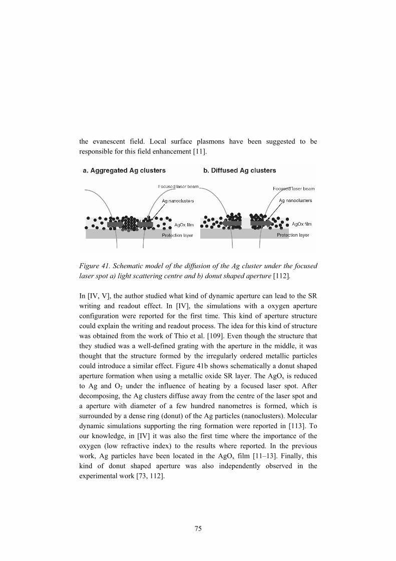
75
the evanescent field. Local surface plasmons have been suggested to be responsible for this field enhancement [11].
Figure 41. Schematic model of the diffusion of the Ag cluster under the focused laser spot a) light scattering centre and b) donut shaped aperture [112].
In [IV, V], the author studied what kind of dynamic aperture can lead to the SR writing and readout effect. In [IV], the simulations with a oxygen aperture configuration were reported for the first time. This kind of aperture structure could explain the writing and readout process. The idea for this kind of structure was obtained from the work of Thio et al. [109]. Even though the structure that they studied was a well-defined grating with the aperture in the middle, it was thought that the structure formed by the irregularly ordered metallic particles could introduce a similar effect. Figure 41b shows schematically a donut shaped aperture formation when using a metallic oxide SR layer. The AgOx is reduced to Ag and O2 under the influence of heating by a focused laser spot. After decomposing, the Ag clusters diffuse away from the centre of the laser spot and a aperture with diameter of a few hundred nanometres is formed, which is surrounded by a dense ring (donut) of the Ag particles (nanoclusters). Molecular dynamic simulations supporting the ring formation were reported in [113]. To our knowledge, in [IV] it was also the first time where the importance of the oxygen (low refractive index) to the results where reported. In the previous work, Ag particles have been located in the AgOx film [11�13]. Finally, this kind of donut shaped aperture was also independently observed in the experimental work [73, 112].
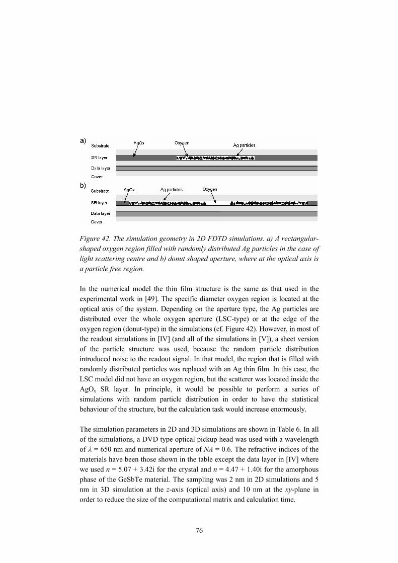
76
Figure 42. The simulation geometry in 2D FDTD simulations. a) A rectangular-shaped oxygen region filled with randomly distributed Ag particles in the case of light scattering centre and b) donut shaped aperture, where at the optical axis is a particle free region.
In the numerical model the thin film structure is the same as that used in the experimental work in [49]. The specific diameter oxygen region is located at the optical axis of the system. Depending on the aperture type, the Ag particles are distributed over the whole oxygen aperture (LSC-type) or at the edge of the oxygen region (donut-type) in the simulations (cf. Figure 42). However, in most of the readout simulations in [IV] (and all of the simulations in [V]), a sheet version of the particle structure was used, because the random particle distribution introduced noise to the readout signal. In that model, the region that is filled with randomly distributed particles was replaced with an Ag thin film. In this case, the LSC model did not have an oxygen region, but the scatterer was located inside the AgOx SR layer. In principle, it would be possible to perform a series of simulations with random particle distribution in order to have the statistical behaviour of the structure, but the calculation task would increase enormously.
The simulation parameters in 2D and 3D simulations are shown in Table 6. In all of the simulations, a DVD type optical pickup head was used with a wavelength of λ = 650 nm and numerical aperture of NA = 0.6. The refractive indices of the materials have been those shown in the table except the data layer in [IV] where we used n = 5.07 + 3.42i for the crystal and n = 4.47 + 1.40i for the amorphous phase of the GeSbTe material. The sampling was 2 nm in 2D simulations and 5 nm in 3D simulation at the z-axis (optical axis) and 10 nm at the xy-plane in order to reduce the size of the computational matrix and calculation time.

77
Table 6. The modelling parameters used in the super resolution data storage simulations. The refractive index of the data layer in [IV] was 5.07+3.42i for the crystal phase and 4.47+1.40i for the amorphous phase material.
Parameter Symbol Value
Refractive indexes n
ZnS-SiO2 2.2
SR layer (AgOx)
(Ag)
2.50 + 0.11i
0.27 + 4.43i
Data layer (GeSbTe) crystal
amorphous
4.6 + 4.2i
4.2 + 1.9i
Wavelength λ 650 nm
Numerical aperture NA 0.6
Sampling 2D
3D Nλ 325 (2 nm)
130 / 65 (5 / 10 nm)
5.2.1 Writing simulations
When the light scattering centre structure is compared to the donut shaped structure, it is difficult to explain the writing of small data marks with the LSC-type structure. Figure 43 shows the power flow at the boundary between the data layer and the spacer layer between the SR and data layers (cf. Figure 42) for both structures with different aperture diameter and particle density. Here it is assumed that the power flow profile at the surface of the data layer is related to the mark size. In the case of LSC aperture, the curves have a Gaussian-shaped envelope and only the tip is affected by the Ag particles. In addition, regardless of the number of the particles, there is always a hole at the optical axis even in the case when no particles (Ag = 0) exists in the aperture region.
On the other hand, when the donut shaped structure is used, a significant narrowing of the spot size is observed, which could lead to SR writing performance (Figure 43b). In this case, the Ag particle region diameter was 1 µm (cf. Figure 42b) and the Ag density was 50 particles per 100 nm transversal distance. Now the spot size is almost equal to the aperture diameter. If the

78
particle density is lower, the spot size will increase, but it is still smaller than the Gaussian-shaped reference spot. From Figure 42b it is possible to estimate that with a 100 nm aperture, it is possible to write roughly 5 times smaller data marks than with the conventional diffraction limited spot. This would lead to an increase in the linear density (that is in the direction of the data grooves) and approximately 5 times more data on a single layer than a single layer DVD disc. In addition, it might be possible to increase the radial density by making the groove period slightly smaller than in the DVD specifications (0.74 µm [23]).
Figure 43. Power flow at the data layer in the case of a) LSC structure and b) donut shaped structure. RW is the Gaussian beam profile without the SR layer, D is the aperture diameter and Ag is the number of particles (diameter 8 nm) per 100 nm aperture diameter. In the donut shaped structure Ag = 50 and the diameter of the whole region is 1 µm [IV].
Figure 44. The transversal profile of the transmitted spot behind the AgOx-layer measured using near field scanning microscope [114].
In addition, in the case of a donut shaped aperture, the beam shapes presented in [IV] and shown in Figure 43b are identical to the experimental results published in [114] (see Figure 44). In the experimental work, no data layer has been used
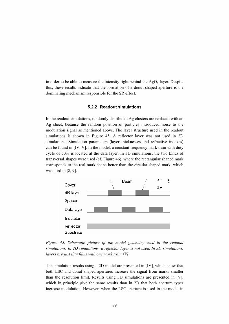
79
in order to be able to measure the intensity right behind the AgOx-layer. Despite this, these results indicate that the formation of a donut shaped aperture is the dominating mechanism responsible for the SR effect.
5.2.2 Readout simulations
In the readout simulations, randomly distributed Ag clusters are replaced with an Ag sheet, because the random position of particles introduced noise to the modulation signal as mentioned above. The layer structure used in the readout simulations is shown in Figure 45. A reflector layer was not used in 2D simulations. Simulation parameters (layer thicknesses and refractive indexes) can be found in [IV, V]. In the model, a constant frequency mark train with duty cycle of 50% is located at the data layer. In 3D simulations, the two kinds of transversal shapes were used (cf. Figure 46), where the rectangular shaped mark corresponds to the real mark shape better than the circular shaped mark, which was used in [8, 9].
Figure 45. Schematic picture of the model geometry used in the readout simulations. In 2D simulations, a reflector layer is not used. In 3D simulations, layers are just thin films with one mark train [V].
The simulation results using a 2D model are presented in [IV], which show that both LSC and donut shaped apertures increase the signal from marks smaller than the resolution limit. Results using 3D simulations are presented in [V], which in principle give the same results than in 2D that both aperture types increase modulation. However, when the LSC aperture is used in the model in

80
[V], there exists the reversal of signals from on-mark and off-marks situations as a function of mark size, which leads to a null point in modulation curve (see Figure 47a). This might be a problem, if the disc would have mark sizes that range over such a null point. In that case, the readout system might not be able to recognise if it is on the mark or between two marks.
Figure 46. 3 different mark trains used in 3D readout simulations. a) smallest mark 150 nm in the case of circular and rectangular marks b) 300 nm circular shaped mark and c) 450 nm x 150 nm rectangular shaped mark [V].
Figure 47b shows the readout modulation as a function of the mark size from the donut shaped aperture. In these simulations, the diameter of the Ag ring is 3x the diameter of the aperture. There is a clear difference in the shape of the modulation curve in comparison with the LSC aperture. Even though the modulation at the resolution limit of the conventional OPH with the donut shaped aperture is about 1/3 from the LSC aperture, the null points do not exist at larger mark sizes. Particularly with 200 nm and 300 nm aperture diameters, the modulation only drops at the 50 nm mark size. In [49], the recording and readout from 100 nm marks was reported with the same disc structure. However, in that work the readout signal was not as good as in [14], where the readout from a 150 nm mark was reported. However, in the latter work the disc structure was not the same as that which is used in this thesis.

81
Figure 47. Readout modulation in the case of a) light scattering centre and b) donut shaped apertures as a function of the circular shaped mark (cf. Figure 46b) with different aperture diameters. Dotted lines are the resolution limit of the DVD OPH (~270 nm) and the corresponding modulation level [V].
In addition, in [V] a set of simulations were performed with a reflector layer as shown in Figure 45. Even though the model predicts (see Figure 48) improved performance in comparison to a non reflector type structure, in the experimental work, the metallic reflector layer (usually Al) has not been used in the SR disc. In conventional DVD-RW design, the reflector layer is used to increase the signal and to fine-tune the modulation from the on-mark and off-marks situations. In addition, it serves as a heat transfer layer during the writing and erasing process.
Figure 48. Readout modulation in the case of a) light scattering centre and b) donut shaped apertures as a function of the rectangular shaped mark (cf. Figure 46c) with different aperture diameters. Dotted lines are the resolution limit of the DVD OPH (~270 nm) and the corresponding modulation level [V].

82
The results in [IV, V] have been obtained with the original idea that the aperture would be dynamic and the modelling results show that marks smaller than the resolution limit can be written and read. However, it has been confirmed in the experimental work that the aperture with the metallic, and also some non-metallic SR layers, is permanent and there is always an aperture at the same location than the mark is written (cf. Figure 9). In simulations by Liu et al. [115], this periodic aperture structure has also taken into account and an improved readout resolution has been reported. In the following section, the author has also used this kind of structure and the idea of the donut shaped aperture structure is modified for the periodic structure.
5.2.3 Nonlinear readout characteristics
The readout carrier to noise ratio from the SR disc is nonlinearly related to the readout power (cf. Figure 49 or [11]). Figure 49 shows the measured CNR for two different SR disc structures. Especially in the case of an elliptical-type structure, there is huge nonlinear increase in the CNR, when the readout power is increased above the threshold of 1.8 mW. In [VI], the author studied using the 2D FDTD model how the drift of the metallic particles away from the centre of the readout laser beam can be responsible for such nonlinear behaviour.
Figure 49. Carrier to noise ration as a function of the readout power from 100 nm marks shown for different SR disc structures [50].

83
It is shown in [112, 113, 116] that the Ag aggregates form a donut shaped aperture centred at the focused laser spot. Figure 50 shows the model geometry where the bubble pit marks (mark size is 300 nm) are formed on the SR layer and the Ag particles are located inside these bubbles (cf. Figure 9). The layer structure is, from top to bottom, ZnS-SiO2/AgOx/ZnS-SiO2/GeSbTe/ZnS-SiO2, where ZnS-SiO2 is dielectric insulating material, AgOx is a super resolution layer and GeSbTe is a phase change data layer. The Figure 50 shows that the layer structure (insulating layer between the SR and data layers, second ZnS-SiO2, and data layer GeSbTe) is deformed after the writing process, as was observed in the experimental work [14, 50, 73]. The Ag particles inside the bubble pits are assumed to move under the influence of the readout laser beam, as was shown by Lin et al. [113]. The size of the region which is affected by the laser spot with different readout power is referred to as an aperture radius. The bubble pits give the outer boundaries to the motion of the particles and therefore the donut-shaped aperture is only formed at the mark on the optical axis of the readout beam. In all of the other bubbles that are within the region affected by the readout beam, the Ag aggregates are located at the furthest edge of the bubble from the optical axis of the beam (see Figure 51).
Figure 50. Bubble pit marks in the initial state after writing the data. Ag particles inside the bubbles are randomly distributed. The top is the on-mark situation and the bottom is the off-mark situation. Mark size is 300 nm. The layer structure of the model is, from top to bottom, ZnS-SiO2/AgOx/ZnS-SiO2/GST/ZnS-SiO2. [IV]

84
Figure 51. Bubble pit marks during the readout when the readout laser power is affecting the Ag particles at the radius of 300 nm. Particles move away from the optical axis and a donut aperture is formed. The top is the on-mark situation and the bottom is the off-mark situation. Mark size is 300 nm. The layer structure of the model is, from top to bottom, ZnS-SiO2/AgOx/ZnS-SiO2/GST/ZnS-SiO2. [IV]
Figure 52 shows the readout modulation calculated from the readout power shown in Figure 53 as a function of the aperture radius. In this case, the silver concentration is 70% from the total volume of the bubble pit. The modulation has a clear threshold after which it increases rapidly and stays almost constant thereafter. The threshold depends on the metal concentration on the formation of the rigid aperture in the bubble pit, which is directly on the optical axis of the readout beam (the middle bubble pit at the on-mark case in Figure 51). At that point, the power at the detector decreases rapidly while the power flow through the aperture increases (see Figure 53). Figure 54 shows the electric field amplitude in the case when the aperture radius is either 0 nm or 150 nm. When the aperture radius is > 75 nm, the metal aperture works as a sub wavelength waveguide and therefore the reflection from the central part of the readout spot decreases significantly in comparison to the case when the aperture diameter is 0 nm.
This behaviour is in agreement with the experimental work shown in Figure 49. The only difference is that in the simulations, the threshold power (aperture radius) is a function of the mark size whereas in the experiments it is constant. That is, as is shown in Figure 52, when the mark size is 150 nm, the threshold is at an aperture radius of 50 nm and when the mark size is 200 nm, the threshold is around an aperture radius of 75 nm. However, it is currently not known how

85
the aperture radius is related to the readout power and therefore it is not possible to plot the modulation in Figure 52 as a function of the readout power.
Figure 52. The modulation of the reflected optical power, as a function of the aperture radius. Silver concentration in the bubble pits is 70% and the initial layer thicknesses are 18, 40 and 60 nm for AgOx, (Spacer) ZnS-SiO2 and GST layers respectively.
Figure 53. The relative power at the detector from on-mark and off-mark cases, as a function of the aperture radius. Silver concentration in bubble pits is 70% and the initial layer thicknesses are 18, 40 and 60 nm for AgOx, (Spacer) ZnS-SiO2 and GST layers respectively.

86
Figure 54. Electric field amplitude at the on-mark case when aperture diameter is either 0 nm or 300 nm (cf. top part of the Figures 44 and 45).
In addition, the results using the model in [VI] also predict that high metal particle concentration give a higher signal than a low concentration. Similar results were also reported in [13] using numerical modelling. However, in Liu�s work, the aperture model within the SR layer was different. In their work, the Ag particles are located in an AgOx background instead of oxygen and they did not use a bubble pit structure but the particles were dispersed over the region illuminated by the readout laser spot.
5.2.4 Quantum and temperature effects
Because of the small size of the metallic particles inside the bubble pits, the quantum effects may change the optical properties of these particles. Figure 55 shows the breakdown of the electric continuum as the metal particle size decreases [117]. When the particle size is large (> 1 µm), the material has a metal properties. However, it will become an insulator, when the diameter of the particle is about 1 nm, which is about 10 atoms. This will certainly affect to the generation of surface plasmons that have been suggested as responsible for the SR readout mechanism [12, 118], because the particle is no longer metallic. The transition of the material properties as a function of the particle size has not been taken into account in this thesis. It would require more detailed study on the optical properties of the small metallic particles and is left for future work.

87
Figure 55. Schematic picture of the fragmentation of the bulk metal. The approximate diameter and other parameters are indicated. The schematic energy level diagram shows the breakdown of the electric continuum as the cluster size decreases. [117]
Heating of the data layer [119], which can lead to a second phase transition [120, 121], is the latest explanation for the readout mechanism for the metallic SR layer medium that forms the bubble pit structure during the writing process. This explanation is based on the fact that in some ferroelectric materials, at a certain temperature range, the dielectric constant changes significantly (ferroelectric catastrophe, see e.g. [122]). GeSbTe and AgInSbTe materials, which are used in the data layer, are ferroelectric materials. Ferroelectric catastrophe could lead to a very narrow aperture that scans the small data marks during the readout. This means that the data marks are now bubble pits and the data layer acts as a super resolution layer, therefore the data layer is still needed even though there is no data marks. However, this mechanism suffers from the fact that, traditionally, the ferroelectric phase transition is only observed with static or very low frequency measurements (see e.g. [123]). On the other hand, the heating effect is supported by work in which no metallic particles exist in the bubble pits of the SR layer [124].

88
6. Conclusions Two different near field optical data storage systems namely direct semiconductor laser readout and super resolution techniques were analyzed using numerical simulation methods. Modelling methods and tools were presented with discussion about the numerical accuracy, boundary and sourcing conditions of the FDTD algorithm. For the validation of the numerical models the results were compared with the experimental and analytical results.
Optimisation results considering the writing conditions using the external cavity configuration were presented, in addition to discussion about the readout performance and the simulations with gain model in the FDTD simulation. Also, when a very small aperture laser configuration was used, the spot size oscillations as a function of the external cavity length was shown for the first time. This phenomena had similar λ/2 periodical behaviour than the output power and wavelength modulation, which have been published earlier. Achievable mark size using the very small aperture laser was at the same order than the aperture diameter and the mark smaller than the resolution limit of the conventional optical pickup head can be written and read.
Both the writing and the readout characteristics of the super resolution disc were studied. The donut shaped aperture model, where the oxygen aperture is surrounded by the silver ring, was proposed. This geometry is similar to one which has been independently observed in the experimental work. In addition, the modelled intensity profile at the surface of the data layer was the same than the measured intensity profile just behind the AgOx-layer. The simulations using the donut shaped aperture in the SR disc show that the marks smaller than 100 nm can be written and read using DVD-type optical pickup head. This is at same order as is obtained in the experimental work and leads to 4x increase in the data density in comparison to the single layer DVD disc.
Nonlinear behaviour of the carrier-to-noise ratio as a function of the readout power was also studied. The numerical model has the same bubble pit structure which has been observed in the experimental work. The particles inside the bubbles are assumed to diffuse away from the optical axis of the focused laser beam and the aperture is formed when the readout power is increased. According to numerical simulations the opening of the central aperture could introduce the nonlinear effect of the carrier-to-noise ratio. Modulation of the readout signal from the 100 nm marks is also achieved using this model.

89
References
1. Mitsuhashi, Y. Optical storage: Science and technology. Japanese Journal of Applied Physics, Part 1: Regular Papers & Short Notes & Review Papers 1998 Apr;37(4B):2079�2083.
2. Milster, T.D. Near-field optics: a new tool for data storage. Proceedings of the IEEE 2000;88(9):1480�1490.
3. Nemoto, K. and Miura, K. A Laser Coupler for DVD/CD Playback Using Monolithic-integrated Two-wavelength Laser Diode. Japan Society of Applied Physics International 2001 January 2001;3:9�14.
4. Kim, J. and Hsieh, H.C. Asymmetry in the optical output power characteristics of a short-external-cavity laser diode. IEEE Photonics Technology Letters 1992;4(6):537�539.
5. Kim, J. and Hsieh, H.C. An open-resonator model for the analysis of a short external-cavity laser diode and its application to the optical disk head. Journal of Lightwave Technology 1992;10(4):439�447.
6. Ukita, H. and Katagiri, Y. Optimum reflectivity design of laser diode facets and recording medium for an integrated flying optical head. Japanese Journal of Applied Physics, Part 1 (Regular Papers & Short Notes) 1993 11/;32(11B):5292�5300.
7. Ye, S., Mitsugi, S., Kim, Y. and Goto, K. Numerical simulation of readout using optical feedback in the integrated vertical cavity surface emitting laser microprobe head. Japanese Journal of Applied Physics, Part 1: Regular Papers & Short Notes & Review Papers 2002;41(3 B):1636�1637.
8. Peng, C. Superresolution near-field readout in phase-change optical disk data storage. Applied Optics 2001;40(23):3922�3931.
9. Nakano, T., Yamakawa, Y., Tominaga. J. and Atoda, N. Near-field optical simulation of super-resolution near-field structure disks. Japanese Journal

90
of Applied Physics, Part 1: Regular Papers & Short Notes & Review Papers 2001;40(3 B):1531�1535.
10. Milster, T., Butz, J.J., Nakano, T., Tominaga, J. and Bletscher, W.L. Signal power in the angular spectrum of AgOx SuperRENS media. In: Tominaga, J. and Tsai, D.P. (ed.) Optical nanotechnologies. Manipulation of surface and local plasmons: Springer-Verlag; 2003. P. 119�139.
11. Liu, W., Wen, C., Chen, K., Lin, W.C. and Tsai, D.P. Near-field images of the AgOx-type super-resolution near-field structure. Applied Physics Letters 2001;78(6):685�687.
12. Liu, W. and Tsai, D.P. Nonlinear near-field optical effects of the AgOx-type super-resolution near-field structure. Japanese Journal of Applied Physics, Part 1: Regular Papers & Short Notes & Review Papers 2003;42(2 B):1031�1032.
13. Liu, W., Ng, M. and Tsai, D.P. Surface plasmon effects on the far-field signals of AgOx-type super resolution near-field structure. Japanese Journal of Applied Physics, Part 1: Regular Papers & Short Notes & Review Papers 2004;43(7 B):4713�4717.
14. Kikukawa, T., Nakano, T., Shima, T. and Tominaga, J. Rigid bubble pit formation and huge signal enhancement in super-resolution near-field structure disk with platinum-oxide layer. Applied Physics Letters 2002 12/16;81(25):4697�4699.
15. Wu, Y., Khoo, H. and Kogure, T. Read-only optical disk with superresolution. Applied Physics Letters 1994;64(24):3225�3227.
16. Wu, Y. and Mohamed, Noor Yb. Calculations on modulation transfer function of a read-only optical disk system with super resolution. Applied Physics Letters 1995;66(8):911�913.
17. Wu, Y. and Chong, C.T. Theoretical analysis of a thermally induced superresolution optical disk with different readout optics. Applied Optics 1997;36(26):6668�6677.

91
18. Taflove, A. and Hagness, S.C. Computational electrodynamics: the finite-difference time-domain method. 2nd ed. Boston: Artech House; 2000.
19. Aikio, J. and Howe, D.G. Direct semiconductor laser readout in optical data storage. Proceedings of SPIE � The International Society for Optical Engineering 2000 Optical Data Storage 2000, May 14�May 17 2000, Whistler, BC, Can;4090:56�65.
20. Partovi, A., Peale, D., Wuttig, M., Murray, C.A., Zydzik, G., Hopkins, L., Baldwin, K., Hobson, W.S., Wynn, J., Lopata, J., Dhar, L., Chichester, R. and Yeh, J.H. High-power laser light source for near-field optics and its application to high-density optical data storage. Applied Physics Letters 1999;75(11):1515�1517.
21. Kataja, K. and Aikio, J. Near field beam properties of the Very Small Aperture Laser Innovative Mass Storage Technologies Technical digest 2002 September 16�17, Exeter, UK:Mo1C2.
22. Marchant, A.B. Optical Recording � A Technical Overview. New York: Addison-Wesley; 1990.
23. ECMA International. 120 mm DVD � Read-Only Disk. 2001;ECMA-267.
24. Stan, S.G. The CD-ROM drive: a brief system description. Boston: Kluwer Academic Publishers; 1998.
25. Cellitti, D.R. World On A Silver Platter, A Brief History Of Optical Disc. Widescreen Review Laser Magic. 1998:14.
26. Gregg, D.P, inventor. Discovision Associates, assignee. Disc-shaped member. California/USA patent 4893297. 1990 January 9.
27. Philips Electronics, Sony Corporation. Compact-Disc Digital Audio. System Description. 1981.
28. Philips Electronics, Sony Corporation. Compact-Disc Read-Only Memory. System Description. 1984.

92
29. Flaherty, N. Battle of the blues. IEE Review 2004;50(4):48�50.
30. Yamamoto, K., Osato, K., Ichimura, I., Maeda, F. and Watanabe, T. 0.8-numerical-aperture two-element objective lens for the optical disk. Japanese Journal of Applied Physics, Part 1: Regular Papers & Short Notes & Review Papers 1997 01/;36(1B):456�459.
31. Yokogawa, F., Ohsawa, S., Iida, T., Araki, Y., Yamamoto, K. and Moriyama, Y. The path from a digital versatile disc (DVD) using a red laser to a DVD using a blue laser. Japanese Journal of Applied Physics, Part 1: Regular Papers & Short Notes & Review Papers 1998 APR;37(4B):2176�2178.
32. van Heerden, P.J. Theory of Optical Information Storage in Solids. Applied Optics 1963;2(4):393�400.
33. Psaltis, D. and Burr, G.W. Holographic data storage. Computer 1998;31(2):52�60.
34. Spielman, S., Johnson, B.V., McDermott, G.A., O'Neill, M.P., Pietrzyk, C., Shafaat, T., Warland, D.K. and Wong, T.L. Using pit-depth modulation to increase capacity and data transfer rate in optical discs. Proceedings of SPIE � The International Society for Optical Engineering 1997;3109:98�104.
35. Ohta, T., Nishiuchi, K., Narumi, K., Kitaoka, Y., Ishibashi, H., Yamada, N. and Kozaki, T. Overview and the future of phase-change optical disk technology. Japanese Journal of Applied Physics, Part 1: Regular Papers & Short Notes & Review Papers 2000;39(2B):770�774.
36. Mansfield, S.M. and Kino, G.S. Solid immersion microscope. Applied Physics Letters 1990 12/10;57(24):2615�2616.
37. Mansfield, S.M., Studenmund, W.R., Kino, G.S. and Osato, K. High-numerical-aperture lens system for optical storage. Optics Letters 1993;18(4):305�307.

93
38. Terris, B.D., Mamin, H.J. and Rugar, D. Optical data storage using a solid immersion lens. Optoelectronics � Devices and Technologies 1995;10(3):303�310.
39. Betzig, E., Trautman, J.K., Wolfe, R., Gyorgy, E.M., Finn, P.L., Kryder, M.H. and Chang, C. Near-field magneto-optics and high density data storage. Applied Physics Letters 1992;61(2):142�144.
40. Hosaka, S., Shintani, T., Miyamoto, M., Hirotsune, A., Terao, M., Yoshida, M., Fujita, K. and Kammer, S. Nanometer-sized phase-change recording using a scanning near-field optical microscope with a laser diode. Japanese Journal of Applied Physics, Part 1: Regular Papers & Short Notes & Review Papers 1996;35(1B):443�447.
41. Betzig, E., Grubb, S.G., Chichester, R.J., DiGiovanni, D.J. and Weiner, J.S. Fiber laser probe for near-field scanning optical microscopy. Applied Physics Letters 1993;63(26):3550�3552.
42. Ukita, H., Katagiri, Y. and Fujimori, S. Supersmall Flying Optical Head for Phase-Change Recording Media. Applied Optics 1989 OCT 15;28(20):4360�4365.
43. Ukita, H., Sugiyama, Y., Nakada, H. and Katagiri, Y. Read/write performance and reliability of a flying optical head using a monolithically integrated LD-PD. Applied Optics 1991;30(26):3770�3776.
44. Goto, K., Sato, T. and Mita, S. Proposal of optical floppy disk head and preliminary spacing experiment between lensless head and disk. Japanese Journal of Applied Physics, Part 1: Regular Papers & Short Notes & Review Papers 1993;32(11B):5459�5460.
45. Tanaka, K., Ohkubo, T., Oumi, M., Mitsuoka, Y., Nakajima, K., Hosaka, H. and Itao, K. Numerical simulation on read-out characteristics of the planar aperture-mounted head with a minute scatterer. Japanese Journal of Applied Physics, Part 1: Regular Papers & Short Notes & Review Papers 2001;40(3 B):1542�1547.

94
46. Yoshikawa, H., Andoh, Y., Yamamoto, M., Fukuzawa, K., Tamamura, T. and Ohkubo, T. 7.5-MHz data-transfer rate with a planar aperture mounted upon a near-field optical slider. Optics Letters 2000;25(1):67�69.
47. Bouwhuis, G. and Spruit, J.H.M. Optical storage read-out of nonlinear disks [optical scanning microscopy]. Applied Optics 1990;29(26):3766�3768.
48. Tominaga, J., Nakano, A.T. and Atoda, N. An approach for recording and readout beyond the diffraction limit with an Sb thin film. Applied Physics Letters 1998 10/12;73(15):2078�80.
49. Fuji, H., Tominaga, J., Men, L., Nakano, T., Katayama, H. and Atoda, N. Near-field recording and readout technology using a metallic probe in an optical disk. Japanese Journal of Applied Physics, Part 1: Regular Papers & Short Notes & Review Papers 2000;39(2B):980�981.
50. Kim, J., Hwang, I., Yoon, D., Park, I., Shin, D., Kikukawa, T., Shima, T. and Tominaga, J. Super-resolution by elliptical bubble formation with PtOx and AgInSbTe layers. Applied Physics Letters 2003;83(9):1701�1703.
51. Terris, B.D., Mamin, H.J., Rugar, D., Studenmund, W.R. and Kino, G.S. Near-field optical data storage using a solid immersion lens. Applied Physics Letters 1994 07/25;65(4):388�390.
52. Tang, S., Milster, T.D., Erwin, J.K. and Bletscher, W.L. High-performance readout and recording by a combination aperture. Optics Letters 2001;26(24):1987�1989.
53. Hayashida, N., Hirata, H., Komaki, T., Usami, M., Ushida, T., Itoh, H., Yoneyama, K. and Utsunomiya, H. High-performance hard coat for cartridge-free Blu-ray disc. Japanese Journal of Applied Physics, Part 1: Regular Papers & Short Notes & Review Papers 2003;42(2 B):750�753.
54. Chang, D., Yoon, D., Ro, M., Hwang, I., Park, I. and Shin, D. Synthesis and characteristics of protective coating on thin cover layer for high density-digital versatile disc. Japanese Journal of Applied Physics, Part 1: Regular Papers & Short Notes & Review Papers 2003;42(2 B):754�758.

95
55. Mitsuhashi, Y., Morikawa, T., Sakurai, K., Seko, A. and Shimada, J. Self-coupled optical pickup. Optics Communications 1976 04/;17(1):95�97.
56. Seko, A., Mitsuhashi, Y., Morikawa, T., Shimada, J. and Sakurai, K. Self-quenching in semiconductor lasers and its applications in optical memory readout. Applied Physics Letters 1975 08/01;27(3):140�141.
57. Mitsuhashi, Y., Shimada, J. and Mitsutsuka, S. Voltage change across the self-coupled semiconductor laser. IEEE Journal of Quantum Electronics 1981;17(7):1216�1225.
58. Ukita, H., Nakada, H. and Abe, T. Improvement in lasing properties of an integrated flying optical head with a diamond-film-coated slider. Japanese Journal of Applied Physics, Part 1 (Regular Papers & Short Notes) 1992 02/;31(2B):524�528.
59. Katagiri, Y.and Ukita, H. Ion beam sputtered (SiO2)x(Si3N4)1-x antireflection coatings on laser facets produced using O2-N2 discharges. Applied Optics 1990 12/01;29(34):5074�5079.
60. Goto, K., Kim, Y.and Hasegawa, Y. Experiments of noble optical floppy disk drive using phase change optical medium and quasi-near field optical head. Proceedings of SPIE � The International Society for Optical Engineering 1999;3864:62�64.
61. Kim, Y., Hasegawa, Y. and Goto, K. Development of a novel optical floppy disk drive using a phase change optical medium and a quasi-near-field optical head. Japanese Journal of Applied Physics, Part 1: Regular Papers & Short Notes & Review Papers 2000;39(2B):929�932.
62. Goto, K. Proposal of ultrahigh density optical disk system using a vertical cavity surface emitting laser array. Japanese Journal of Applied Physics, Part 1: Regular Papers & Short Notes & Review Papers 1998;37(4B):2274�2278.
63. Kim, Y., Suzuki, K and Goto, K. Parallel recording array head of nano-aperture flat-tip probes for high-density near-field optical data storage.

96
Japanese Journal of Applied Physics, Part 1: Regular Papers & Short Notes & Review Papers 2001;40(3 B):1783�1789.
64. Goto, K., Kim, Y., Mitsugi, S., Suzuki, K., Kurihara, K. and Horibe, T. Microoptical two-dimensional devices for the optical memory head of an ultrahigh data transfer rate and density system using a vertical cavity surface emitting laser (VCSEL) array. Japanese Journal of Applied Physics, Part 1: Regular Papers & Short Notes & Review Papers 2002;41(7 B):4835�4840.
65. Nikolov, I.D., Goto, K., Mitsugi, S., Kim, Y.J. and Kavardjikov, V.I. Nanofocusing recording probe for an optical disk memory. Nanotechnology 2002;13(4):471�477.
66. Nikolov, I.D., Kurihara, K. and Goto, K. Nanofocusing probe optimization with anti-reflection coatings for a high-density optical memory. Nanotechnology 2003;14(9):946�954.
67. Goto, K., Kirigaya, T., Masuda, Y., Kim, Y., Miyamoto, Y. and Arai, S. Design and experiments of a near-field optical disk head for very high efficiency. Scanning 2004;26(5 SUPPL):68�72.
68. Kikukawa, T., Kato, T., Shingai, H. and Utsunomiya, H. High-density read-only memory disc with super resolution reflective layer. Japanese Journal of Applied Physics, Part 1: Regular Papers & Short Notes & Review Papers 2001;40(3 B):1624�1628.
69. Shi, L.P., Chong, T.C., Miao, X.S., Tan, P.K. and Li, J.M. A new structure of super-resolution near-field phase-change optical disk with a Sb2Te3 mask layer. Japanese Journal of Applied Physics, Part 1: Regular Papers & Short Notes & Review Papers 2001;40(3 B):1649�1650.
70. Qiying, C., Tominaga, J., Men, L., Fukaya, T., Atoda, N. and Fuji, H. Superresolution optical disk with a thermoreversible organic thin film. Optics Letters 2001 03/01;26(5):274�276.
97
71. Lin, W.C., Kao, T.S., Chang, H.H., Lin, Y.H., Fu, Y.H., Wu, C.T., Chen, K.H. and Tsai, D.P. Study of a super-resolution optical structure: Polycarbonate/ZnS-SiO2/ZnO/ZnS-SiO2/Ge2Sb2 Te5/ZnS-SiO2. Japanese Journal of Applied Physics, Part 1: Regular Papers & Short Notes & Review Papers 2003;42(2 B):1029�1030.
72. Liu, Q., Kim, J., Fukaya, T. and Tominaga, J. Thermal-induced optical properties of a PdOx mask layer in an optical data storage system with a superresolution near-field structure. Optics Express 2003;11(21):2646�2653.
73. Takashi, K., Tachibana, A., Fuji, H. and Tominaga, J. Recording and readout mechanisms of super-resolution near-field structure disc with silver-oxide layer. Japanese Journal of Applied Physics, Part 1: Regular Papers & Short Notes & Review Papers 2003;42(2 B):1038�1039.
74. Aikio, J.K. Extremely short external cavity (ESEC) laser devices. Wavelength tuning and related optical characteristics. VTT Publications 529. Technical Research Center of Finland, Espoo, Finland: VTT Electronics; 2004. 163 p.
75. Råde, L. and Westergren, B. Mathematics handbook for science and engineering. 4th ed. Berlin; New York; Lund, Sweden: Springer; Student-litteratur; 1999.
76. Coldren, L.A. and Corzine, S.W. Diode lasers and photonic integrated circuits. New York: Wiley; 1995.
77. Chuang, S.L. Physics of Optoelectronic Devices. New York: Wiley-Interscience; 1995.
78. Wartak, M.S., Weetman, P., Alajoki, T., Aikio, J. and Heikkinen, V. Extraction of rate-equation parameters from optical modal gain measurements for multiple-quantum-well semiconductor lasers. Microwave and Optical Technology Letters 2002;35(1):55�56.
79. Hakki, B.W. and Paoli, T.L. Gain spectra in GaAs double-heterostructure injection lasers. Journal of Applied Physics 1975;46(3):1299�1306.

98
80. Balanis, C.A. Advanced engineering electromagnetics. New York: Wiley; 1989.
81. Liu, W. and Kowarz, M.W. Vector diffraction from subwavelength optical disk structures: Two-dimensional near-field profiles. Optics Express 1998;2(5):191�197.
82. Yee, K. Numerical solution of inital boundary value problems involving Maxwell's equations in isotropic media. IEEE Transactions on Antennas and Propagation 1966;12(3):302�307.
83. Liu, Y. Fourier analysis of numerical algorithms for the Maxwell equations. Journal of Computational Physics 1996 03/15;124(2):396�416.
84. Jurgens, T.G., Taflove, A., Umashankar, K. and Moore, T.G. Finite-difference time-domain modeling of curved surfaces [EM scattering]. IEEE Transactions on Antennas and Propagation 1992 04/;40(4):357�366.
85. Gropp, W., Lusk, E. and Skjellum, A. Using MPI: portable parallel programming with the message-passing interface. 2nd ed. Cambridge, Mass.: MIT Press; 1999.
86. Born, M. and Wolf, E. Principles of optics: electromagnetic theory of propagation, interference and diffraction of light. 6th (corr.) ed. Cambridge, UK; New York: Cambridge University Press; 1997.
87. Okoniewski, M., Mrozowski, M. and Stuchly, M.A. Simple treatment of multi-term dispersion in FDTD. IEEE Microwave and Guided Wave Letters 1997;7(5):121�123.
88. Olkkonen, J. Parallel FDTD algorithm for the analysis of rewritable optical storage systems. Oulu: University of Oulu; 2002.
89. Schneider, J.B. and Wagner, C.L. FDTD dispersion revisited: faster-than-light propagation. Microwave and Guided Wave Letters, IEEE [see also IEEE Microwave and Wireless Components Letters] 1999;9(2):54�56.

99
90. Sadiku, M.N.O., Agbo, S.O. and Bemmel, V. Stability criterion for finite-difference time-domain algorithm. Conference Proceedings � IEEE SOUTHEASTCON 1990 1�4 April, New Orleans, LA, USA;1:48�50.
91. Mur, G. Absorbing boundary conditions for the finite-difference approximation of the time-domain electromagnetic-field equations. IEEE Transactions on Electromagnetic Compatibility 1981;23(4):377�382.
92. Berenger, J. Three-dimensional perfectly matched layer for the absorption of electromagnetic waves. Journal of Computational Physics 1996;127(2):363�379.
93. Berenger, J. A perfectly matched layer for the absorption of electromagnetic waves. Journal of Computational Physics 1994 10/;114(2):185�200.
94. Berenger, J. Improved PML for the FDTD solution of wave-structure interaction problems. IEEE Transactions on Antennas and Propagation 1997;45(3):466�473.
95. Sacks, Z.S., Kingsland, D.M., Lee, R. and Lee, J. A perfectly matched anisotropic absorber for use as an absorbing boundary condition. IEEE Transactions on Antennas and Propagation 1995;43(12):1460�1463.
96. Ziolkowski, R.W. Time-derivative Lorentz material model-based absorbing boundary condition. IEEE Transactions on Antennas and Propagation 1997;45(10):1530�1535.
97. Gedney, S.D. An anisotropic perfectly matched layer-absorbing medium for the truncation of FDTD lattices. IEEE Transactions on Antennas and Propagation 1996 12/;44(12):1630�9.
98. Yariv, A. Optical electronics. 4th ed. Philadelphia: Saunders College Pub.; 1991.
99. Goodman, J.W. Introduction to Fourier optics. 2nd ed. New York: McGraw-Hill; 1996.

100
100. Peng, C. and Mansuripur, M. Sources of noise in erasable optical disk data storage. Applied Optics 1998;37(5):921�928.
101. Jin, J. The finite element method in electromagnetics. 2nd ed. New York: Wiley; 2002.
102. Itagi, A.V., Challener, W.A., Sendur, I.K. and Schlesinger, T.E. Finite difference frequency domain scattered field formulation for near-field optical data storage. Proceedings of SPIE � The International Society for Optical Engineering 2004 September;5380:351�359.
103. Ikegami, T. Reflectivity of mode at facet and oscillation mode in double-heterostructure injection lasers. IEEE Journal of Quantum Electronics 1972;QE-8(6):470�476.
104. Herzinger, C.M., Lu, C.C., DeTemple, T.A. and Chew, W.C. Semiconductor waveguide facet reflectivity problem. IEEE Journal of Quantum Electronics 1993;29(8):2273�2281.
105. Fluckiger, D. Grating Solver Product Information. 22 December 2004; Available at: www.gsolver.com. Accessed 30 March, 2005.
106. Moharam, M.G. and Gaylord, T.K. Rigorous coupled-wave analysis of planar-grating diffraction. Journal of the Optical Society of America 1981;71(7):811�818.
107. Hagness, S.C., Joseph, R.M. and Taflove, A. Subpicosecond electrodynamics of distributed Bragg reflector microlasers: results from finite difference time domain simulations. Radio Science 1996;31(4):931�941.
108. Uenishi, Y., Isomura, Y., Sawada, R., Ukita, H. and Toshima, T. Beam converging laser diode by taper ridge waveguide. Electronics Letters 1988 12 May;24(10):623�624.
109. Thio, T., Pellerin, K.M., Linke, R.A., Lezec, H.J. and Ebbesen, TW. Enhanced light transmission through a single subwavelength aperture. Optics Letters 2001;26(24):1972�1974.
101
110. Thio, T., Lezec, H.J., Ebbesen, T.W., Pellerin, K.M., Lewen, G.D., Nahata, A. and Linke, R.A. Giant optical transmission of sub-wavelength apertures: Physics and applications. Nanotechnology 2002;13(3):429�432.
111. On surface plasmon enhanced near-field transducers. Optical Data Storage 2004, Apr 18�21 2004 Monterey, CA, United States: International Society for Optical Engineering, Bellingham, WA 98227-0010, United States; 2004.
112. Ho, F.H., Chang, H.H., Lin, Y.H., Chen, B., Wang, S. and Tsai, D.P. Functional structures of AgOx thin film for near-field recording. Japanese Journal of Applied Physics, Part 1: Regular Papers & Short Notes & Review Papers 2003;42(2 B):1000�1004.
113. Lin, B.S., Tsai, D.P. and Lin, W.C. Molecular dynamics simulations for the aggregation of silver clusters in the AgOx-type super-resolution near-field structure. International Symposium on Optical Memory Technical Digest 2003 November 3�7, Nara Japan:Th-H-02.
114. Lin, W.C., Su, J.D., Tsai, M.C., Tsai, D.P., Lu, N.H., Huang, H.J. and Lin, W.Y. Study of the mechanism of the light-scattering-mode super-resolution near-field structure. Proceedings of SPIE � The International Society for Optical Engineering 2001;4416:231�235.
115. Liu, W., Ng, M. and Tsai, D.P. Enhanced resolution of AgOx-type super-RENS disks with periodic silver nanoclusters. Scanning 2004;26(5 SUPPL):98�101.
116. Her, Y., Lan, Y., Hsu, W. and Tsai, S. Recording and readout mechanisms of super-resolution near-field structure disk with. Applied Physics Letters 2003;83(11):2136�2138.
117. Rao, C. N. R., Kulkarni, G.U., Thomas, P.J. and Edwards, P.P. Metal nanoparticles and their assemblies. Chemical Society Reviews 2000;29(1):27�35.
118. Tominaga, J., Kim, J., Fuji, H., Buchel, D., Kikukawa, T., Men, L., Fukuda, H., Sato, A., Nakano, T., Tachibana, A., Yamakawa, Y., Kumagai, M.,

102
Fukaya, T. and Atoda, N. Super-resolution near-field structure and signal enhancement by surface plasmons. Japanese Journal of Applied Physics, Part 1: Regular Papers & Short Notes & Review Papers 2001;40(3 B):1831�1834.
119. Kuwahara, M., Shima, T., Kolobov, A. and Tominaga, J. Thermal origin of readout mechanism of light-scattering super-resolution near-field structure disk. Japanese Journal of Applied Physics, Part 2 (Letters) 2004 01/15;43(1A/B):8�10.
120. Tominaga, J., Shima, T., Kuwahara, M., Fukaya, T., Kolobov, A. and Nakano, T. Ferroelectric catastrophe: Beyond nanometre-scale optical resolution. Nanotechnology 2004;15(5):411�415.
121. Kolobov, A.V., Fons, P., Frenkel, A.I., Ankudinov, A.L., Tominaga, J., and Uruga, T. Understanding the phase-change mechanism of rewritable optical media. Nature Materials 2004;3(10):703�708.
122. Dove, M.T. Structure and dynamics: an atomic view of materials. Oxford; New York: Oxford University Press; 2003.
123. Pollina, R.J. and Garland, C.W. Dielectric and ultrasonic measurements in CsH2AsO4. Physical Review B (Solid State) 1975 07/01;12(1):362�367.
124. Shima, T., Kuwahara, M., Fukaya, T., Nakano, T. and Tominaga, J. Super-resolutional readout disk with metal-free phthalocyannic recording layer. Japanese Journal of Applied Physics, Part 2 (Letters) 2004 01/15;43(1A/B):88�90.
Appendices of this publication are not included in the PDF version. Please order the printed version to get the complete publication (http://www.vtt.fi/inf/pdf/)
Published by
Series title, number and report code of publication
VTT Publications 570 VTT�PUBS�570
Author(s) Kataja, Kari J. Title
Numerical modelling of near field optical data storage
Abstract In this thesis, two future generation optical data storage techniques are studied using numerical models. Direct semiconductor laser readout (DSLR) system employs external cavity configuration and super resolution (SR) technique an optically nonlinear material layer at the optical disc for recording and readout operation. Work with the DSLR system is focused on the studying and optimisation of the writing performance of the system, while work with the SR system has focused on explaining the physical phenomena responsible for SR readout and writing performance. Both techniques enable the writing and readout of the data marks smaller than the resolution limit of the conventional optical pickup head. Using SR technique 4x increase in the data density in comparison to DVD disk can be obtained. Because the studied structures are in the order of the wavelength, ray tracing and scalar methods cannot be used to model the system. But, the solution of Maxwell�s vector equations is required in order to study these structures. Moreover, analytical solutions usually do not exist for such complex structures, thus the numerical methods have to be used. In this thesis the main modelling tool has been the Finite Difference Time Domain method.
Keywords direct semiconductor laser readout system DSLR, super resolution technique SR, Finite Difference Time Domain method FDTD, numerical methods
Activity unit VTT Electronics, Kaitoväylä 1, P.O.Box 1100, FI�90571 OULU, Finland
ISBN Project number 951�38�6653�X (soft back ed.) 951�38�6654�8 (URL:http://www.inf.vtt.fi/pdf/)
Date Language Pages Price August 2005 English 102 p. + app. 63 p. D
Name of project Commissioned by
Series title and ISSN Sold by
VTT Publications 1235�0621 (soft back ed.) 1455�0849 (URL: http://www.vtt.fi/inf/pdf/)
VTT Information Service P.O.Box 2000, FI�02044 VTT, Finland Phone internat. +358 20 722 4404 Fax +358 20 722 4374

VTT PU
BLICATIO
NS 570
Num
erical modelling of near field optical data storage
Kari J. K
ataja
Tätä julkaisua myy Denna publikation säljs av This publication is available from
VTT TIETOPALVELU VTT INFORMATIONSTJÄNST VTT INFORMATION SERVICEPL 2000 PB 2000 P.O.Box 2000
02044 VTT 02044 VTT FI–02044 VTT, FinlandPuh. 020 722 4404 Tel. 020 722 4404 Phone internat. +358 20 722 4404Faksi 020 722 4374 Fax 020 722 4374 Fax +358 20 722 4374
ISBN 951–38–6653–X (soft back ed.) ISBN 951–38–6654–8 (URL: http://www.vtt.fi/inf/pdf/)ISSN 1235–0621 (soft back ed.) ISSN 1455–0849 (URL: http://www.vtt.fi/inf/pdf/)
ESPOO 2005ESPOO 2005ESPOO 2005ESPOO 2005ESPOO 2005 VTT PUBLICATIONS 570
Kari J. Kataja
Numerical modelling of near fieldoptical data storage
In this thesis, two future generation optical data storage techniques arestudied using numerical models. Direct semiconductor laser readout (DSLR)system employs external cavity configuration and super resolution (SR)technique an optically nonlinear material layer at the optical disc forrecording and readout operation. Work with the DSLR system is focused onthe studying and optimisation of the writing performance of the system,while work with the SR system has focused on explaining the physicalphenomena responsible for SR readout and writing performance. Bothtechniques enable the writing and readout of the data marks smaller thanthe resolution limit of the conventional optical pickup head. Using SRtechnique 4x increase in the data density in comparison to DVD disk can beobtained. Because the studied structures are in the order of the wavelength,ray tracing and scalar methods cannot be used to model the system. But, thesolution of Maxwell's vector equations is required in order to study thesestructures. Moreover, analytical solutions usually do not exist for suchcomplex structures, thus the numerical methods have to be used. In thisthesis the main modelling tool has been the Finite Difference Time Domainmethod.