NRI INSTITUTE OF TECHNOLOGY VLSI LABORATORY MANUAL DEPARTMENT OF ELECTRONICS AND COMMUNICATION...
49
1 VLSI LABORATORY MANUAL DEPARTMENT OF ELECTRONICS AND COMMUNICATION ENGINEERING NRI INSTITUTE OF TECHNOLOGY (Approved by AICTE, New Delhi: Affiliated to JNTUK, Kakinada) POTHAVARAPPADU (V), (via) Nunna, Agiripalli (M), Krishna District, A.P. PIN: 521212 Ph: 08656-324999 Website: nrigroupofcolleges.com e-mail: [email protected]
-
Upload
nguyenkiet -
Category
Documents
-
view
218 -
download
3
Transcript of NRI INSTITUTE OF TECHNOLOGY VLSI LABORATORY MANUAL DEPARTMENT OF ELECTRONICS AND COMMUNICATION...

1
VLSI LABORATORY MANUAL
DEPARTMENT OF ELECTRONICS AND COMMUNICATION
ENGINEERING
NRI INSTITUTE OF TECHNOLOGY
(Approved by AICTE, New Delhi: Affiliated to JNTUK, Kakinada) POTHAVARAPPADU (V), (via) Nunna, Agiripalli (M), Krishna District, A.P. PIN: 521212 Ph: 08656-324999
Website: nrigroupofcolleges.com e-mail: [email protected]

2
List of Experiments
S. No. Experiment Name
Page No.
Introduction 3
1 CMOS Inverter 10
2 Design and implementation of universal gates 14
3 Design and implementation of full adder 25
4 Design and implementation of full subtractor 28
5 Design and implementation of D-latch 31
6 Design and implementation of RS-latch 34
7 Design and implementation asynchronous counter 37
8. Design and Implementation of static RAM cell 39
9. Design and Implementation of differential amplifier 42
10. Design and Implementation of ring oscillator 45
List of Additional Experiments
S. No. Experiment Name
Page No.
1 Current Mirror 49
2 Operational Amplifier 52
3 TRANS CONDUCTANCE AMPLIFIER 55
4 Design Of A 10 Bit Number Controlled Oscillator 58

3
Introduction In MicroWind, the default icon is the drawing icon shown above. It allows box editing. The
palette is located in the lower right corner of the screen. A red color indicates the current layer.
Initially the selected layer in the palette is polysilicon. The two first steps are illustrated in Figure
2.
Fix the first corner of the box with the mouse. While keeping the mouse button pressed, move the mouse to the opposite corner of the box. Release the button. This creates a box in polysilicon layer as shown in Figure 2. The box width should
not be lower than 2 λ, which is the minimum width of the polysilicon box.
Fig. 2. Creating a polysilicon box.
Now, draw two more boxes as in Figure 3. Try to keep close to the shape and size shown in
Figure.
Fig. 3. Creating three polysilicon boxes.

4
Change the current layer into N+ diffusion by a click in the palette on the Diffusion N+ button. Be
sure that the red layer is now the N+ Diffusion. Draw a n-diffusion box at the bottom of the drawing as
in Figure 4. N-diffusion boxes are represented in green. The intersection between the N+ diffusion and
the polysilicon creates the channel of the MOS device.
Fig. 4. Creating the N-channel and P-Channel devices. Change the current layer into P+ diffusion by a click in the palette on the button P+ Diffusion. Draw a
p-diffusion box at the top of the drawing as in Figure 4. P-diffusion boxes are represented in yellow.
The intersection between the P+ diffusion and the polysilicon creates the channel of the pMOS device.
Change the current layer into N Well by a click on the corresponding button in the palette. Draw a
well all around the p+ diffusion, as in Figure 5. Use keyboard arrows (up key) to view the upper part
of the layout.
Fig. 5. Creating the well for the P-Channel Device.

5
Process Simulation
Click on this icon to access « process simulation ». The cross-section is given by a click on the
mouse at the first point and the release of the mouse at the second point. In the example below
(Figure 6), the cross-section of the n-channel MOS device appears on the left, and the cross-
section of the p-channel MOS device on the right.
Fig. 6. The cross-section of the nMOS and pMOS devices.
Contacts and Metal Interconnects The diffusion areas must be joined using a metal layer. The metal layer is isolated from the diffusions
by a thick silicon dioxide SiO2 layer. The contact layer is used to drill a hole in the oxide in order to
join the metal and the diffusions. You could draw the contact box manually by selecting the layer «
Contact » and drawing a 2 x 2 λ box. A fast solution is to use the predefined macros at the top of the
palette. Various contacts built according to design rules are proposed.
Contact
diffn/metal
Contact Contact poly/metal diffp/metal
Contact via/metal
Fig. 7. The contact macros.
Choose the diffn/metal contact icon in the palette. The contact outline will appear. Fix the contact
inside the n+ diffusion area. Click again on the diffn/metal contact and place it at the upper corner of
the n-well box. This contact is used to polarize the well at VDD. The diffusion N+ in the nwell makes
an ohmic contact and prepares for the VDD polarization using metal layers. Finally, click on the
diffp/metal icon and fix the contact inside the p+ diffusion area.

6
Select the « metal » layer in the palette. Draw a metal bridge between the n+ and p+ contacts. The
CMOS inverter layout is almost completed (Figure 8). The remaining task is to define where the
supply, the ground, the input and the output are.
Fig. 8. The metal bridge and the inverter are completed.
Add Properties for Simulation
Properties must be added to the layout to fix the ground, the supply, the input and the outputs.
The summary of available properties is reported below.
VDD property
VSS property Node visible
Clock property Pulse property
For the inverter example, we must assign the upper p-diffusion to a VDD power supply, and the lower
n-diffusion box to a VSS ground voltage. We also need to specify a clock as the input for the IN node
and have a look at the output OUT. Stuck at Vdd: Click on the Vdd icon and click on the upper p-diffusion box. The Vdd
property is sent to the node.

7
Also click in the N-Well region inside which the pMOS is located. The NWell must
always be at VDD voltage to keep the pMOS junctions inverted.
Hold at Vss: Click on the Vss icon, click on the lower n-diffusion box. The Vss
property is sent to the node. Apply a clock to node IN: Click on the Clock icon and on the polysilicon gate. The
Clock menu appears (See below). Click on OK. A default clock with 3 ns
period is generated. The Clock property is sent to the node and appears at the right
hand side of the desired location with the name « clock1 ».
Fig. 9. The clock menu.
Watch the output: Click on the Visible icon and then, on the metal bridge. The window below appears. Click OK. The Visible property is sent to the node. The associated text « s1 » is in italic. The chronogram of this node will appear in the next
simulation.

8
Analog Simulation
IMPORTANT : Always save BEFORE simulation ! Click on File in the main menu. Move the
cursor to Save as ... and click on it. A new window appears, into which you are to enter the design
name. Type, for example, MYINV. Use the keyboard for this and press ↵. Then click on OK. After a
confirmation question, the design is saved under that filename.
Click on Simulate in the main menu. The timing diagrams of the inverter appear, as shown in Figure
10. Click on More in order to perform more simulations. Click on Stop to return to the editor. The
gate delay is computed at VDD/2, that is 2.5 V, between the signal selected in the Start Node list and
the signal selected with the Stop Node list.
Fig. 10. Analog simulation of the CMOS inverter. The output has the opposite value of the clock input.

9
Click on Voltage & Currents to see both currents and voltages (Figure 10). The current peaks
can be seen in the upper window. All voltages are reported in the lower window. The current
scale can be adjusted using a predefined list of values. Some current is consumed at VDD
supply, mainly when the output of the inverter rises to VDD. Some current is consumed at VSS,
mainly when the output goes down to zero.
Click on Voltage vs. Voltage to see the DC transfer characteristics of the inverter (Figure 11-
bottom). The commutation point of the inverter Vc is the input voltage for which the output is
close to VDD/2. In the case of Figure 24, Vc is around 1.8 V. Click on Back to Editor to return
to the editor.
Fig. 11. Current consumption of the CMOS inverter (top) and DC characteristics of the CMOS inverter(bottom

10
1. CMOS INVERTER
Aim:
a) To design the schematic of CMOS Inverter in Tanner EDA Tools
b) To implement the CMOS Inverter in Microwind Tool.
Tools used:
1. Tanner Tools v13.1
2. Schematic-Edit
3. Layout - Microwind
4. Wave- Edit
THEORY:
CMOS Inverter consists of nMOS and pMOS transistor in series
connected between VDD and GND. The gate of the two transistors are shorted
and connected to the input. When the input to the inverter A = 0, nMOS
transistor is OFF and pMOS transistor is ON. The output is pull-up to VDD.
When the input A = 1, nMOS transistor is ON and pMOS transistor is OFF. The
Output is Pull-down to GND.
Procedure for schematic:
1. Open S-Edit window.
2. Go to File New New design
3. Go to Cell New View
4. Add libraries file to the New Cell.
5. Instance the devices by using appropriate library files.
6. Save the design and setup the simulation.
7. Run design and observe waveforms.
8. Observe DC inputs and outputs by giving appropriate inputs.

11
Procedure for layout :
1. Draw the CMOS Inverter layout by obeying the Lamda Rules using
microwind
i. Poly - 2λ
ii. Active contact - 2 λ
iii. Active Contact – Metal - 1 λ
iv. Active Contact – Active region - 2 λ
v. Active Region – Pselect - 3 λ
vi. Pselect – nWell - 3λ 2. Check DRC to verify whether any region violate the lamda rule
Logic Diagram:

12
Schematic Diagram:
Fig (a): CMOS Inverter
LAYOUT USING MICROWIND:

13
Output responses:
Fig (b): CMOS Inverter Waveforms
Result:
The CMOS Inverter is constructed in Tanner EDA, the layout is
implemented and waveforms are verified.

14
2, LOGIC GATES
Aim:
a) To design the schematic of LOGIC GATES in Tanner EDA Tools
b) To implement the LOGIC GATES in Microwind Tool.
(i) NAND (ii) NOR (iii) OR (iv) AND (v) Ex-OR (vi) Ex-NOR
Tools used:
1. Tanner Tools v13.1
2. Schematic-Edit
3. Layout -MICROWIND
4. Wave- Edit
Procedure:
1. Open S-Edit window.
2. Go to File New New design
3. Go to Cell New View
4. Add libraries file to the New Cell.
5. Instance the devices by using appropriate library files.
6. Save the design and setup the simulation.
7. Run design and observe waveforms.
8. Observe DC inputs and outputs by giving appropriate inputs.
Procedure for layout :
1. Draw the CMOS Inverter layout by obeying the Lamda Rules using
microwind
i. Poly - 2λ
ii. Active contact - 2 λ
v. Active Contact – Metal - 1 λ
vi. Active Contact – Active region - 2 λ
v. Active Region – Pselect - 3 λ
vii. Pselect – nWell - 3λ 2. Check DRC to verify whether any region violate the lamda rule

15
NAND GATE
Logic Diagram:
Schematic Diagram:

16
LAYOUT USING MICROWIND:
SIMULATED WAVEFORM:

17
NORGATE
Logic Diagram:
Schematic Diagram:

18
LAYOUT USING MICROWIND:
SIMULATED WAVEFORM:

19
iii) AND Gate:
Schematic Diagram:
Fig : AND Gate Schematic
Layout Diagram of AND gate:

20
Output responses:
Fig : AND Gate Waveforms

21
(iv) OR Gate:
Logic Diagram:
Fig : OR Gate Schematic
Layout Diagram of OR Gate:

22
Output responses:
Fig : OR Gate Waveforms
(v) Ex-OR Gate:
Fig : Ex-OR Gate Schematic

23
Layout Diagram of XOR Gate:
Output responses: INPUT A
INPUT B
OUTPUT
Fig : Ex-OR Gate Waveforms

24
(vi) Ex-NOR Gate:
Fig : Ex-NOR Gate Schematic
Output responses:
INPUT A
INPUT B
OUTPUT
Fig : Ex-NOR Gate Waveforms
Result:
The Logic gates are constructed in Tanner EDA, the layout is implemented and
waveforms are verified.

25
3. FULL ADDER
Aim:
a) To design the schematic of FULL ADDER in Tanner EDA Tools
b) To implement the FULL ADDER in Microwind Tool.
Tools used:
1. Tanner Tools v13.1
2. Schematic-Edit
3. Layout -MICROWIND
4. Wave- Edit
Procedure:
1. Open S-Edit window.
2. Go to File New New design
3. Go to Cell New View
4. Add libraries file to the New Cell.
5. Instance the devices by using appropriate library files.
6. Save the design and setup the simulation.
7. Run design and observe waveforms.
8. Observe DC inputs and outputs by giving appropriate inputs.
Logic Diagram:

26
Schematic Diagram:
Fig (a): Full Adder Schematic1
Output responses: INPUT V(A)
INPUT V(B)
INPUT V(C)

27
OUTPUT V(SUM)
OUTPUT V(CARRY)
Fig (b): Full Adder wave forms
Layout Diagram of Full adder:
Result:
The Full adder is constructed in Tanner EDA, the layout is implemented and
waveforms are verified.

28
4. FULL SUBTRACTOR
Aim:
a) To design the schematic of FULL SUBTRACTOR in Tanner EDA Tools
b) To implement the FULL SUBTRACTOR in Microwind Tool.
Tools used:
1. Tanner Tools v13.1
2. Schematic-Edit
3. Layout -MICROWIND
4. Wave- Edit
Procedure:
1. Open S-Edit window.
2. Go to File New New design
3. Go to Cell New View
4. Add libraries file to the New Cell.
5. Instance the devices by using appropriate library files.
6. Save the design and setup the simulation.
7. Run design and observe waveforms.
8. Observe DC inputs and outputs by giving appropriate inputs.
Logic Diagram:

29
Schematic Diagram:
Fig (a): Full subtractor Schematic1
Output responses:
Fig (b): Full subtractor wave forms

30
Layout Diagram of Full subtractor:
Result:
The Full subtractor is constructed in Tanner EDA, the layout is implemented and
waveforms are verified.

31
5. D - LATCH
Aim:
a) To design the schematic of D-LATCH in Tanner EDA Tools
b) To implement the D-LATCH in Microwind Tool.
Tools used:
1. Tanner Tools v13.1
2. Schematic-Edit
3. Layout -MICROWIND
4. Wave- Edit
Procedure:
1. Open S-Edit window.
2. Go to File New New design
3. Go to Cell New View
4. Add libraries file to the New Cell.
5. Instance the devices by using appropriate library files.
6. Save the design and setup the simulation.
7. Run design and observe waveforms.
8. Observe DC inputs and outputs by giving appropriate inputs.
Logic Diagram:

32
Schematic Diagram:
Layout Diagram:

33
Output responses:
Fig (b): D-Latch waveforms
Result:
The D-Latch is constructed in Tanner EDA, the layout is implemented and
waveforms are verified.
34
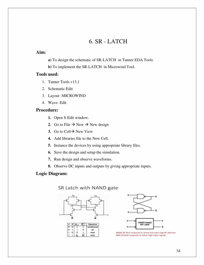
6. SR - LATCH
Aim:
a) To design the schematic of SR-LATCH in Tanner EDA Tools
b) To implement the SR-LATCH in Microwind Tool.
Tools used:
1. Tanner Tools v13.1
2. Schematic-Edit
3. Layout -MICROWIND
4. Wave- Edit
Procedure:
1. Open S-Edit window.
2. Go to File New New design
3. Go to Cell New View
4. Add libraries file to the New Cell.
5. Instance the devices by using appropriate library files.
6. Save the design and setup the simulation.
7. Run design and observe waveforms.
8. Observe DC inputs and outputs by giving appropriate inputs.
Logic Diagram:

35
Schematic Diagram:
Layout Diagram:

36
Output responses:
Fig (b): SR-Latch waveforms
Result:
The SR-Latch is constructed in Tanner EDA, the layout is implemented and
waveforms are verified.

37
7. Asynchronous counter
FOUR BIT ASYNCHRONOUS COUNTER USING T FLIPFLOP
Aim:
a) To construct FOUR BIT ASYNCHRONOUS COUNTER USING T
FLIPFLOP in Tanner EDA
b) To analyze the response with appropriate wave forms
Tools used:
1. Tanner Tools v13.1
2. Schematic-Edit
3. Layout -MICROWIND
4. Wave- Edit
Procedure:
1. Open S-Edit window.
2. Go to File New New design
3. Go to Cell New View
4. Add libraries file to the New Cell.
5. Instance the devices by using appropriate library files.
6. Save the design and setup the simulation.
7. Run design and observe waveforms.
8. Observe DC inputs and outputs by giving appropriate inputs.

38
Result: The Asynchronous Counter is constructed in Tanner EDA, the layout is
implemented and waveforms are verified.

39
8. Ring Oscillator Aim:
a) To design the schematic of Ring Oscillator in Tanner EDA Tools
b) To implement the Ring Oscillator in Microwind Tool.
Tools used:
1. Tanner Tools v13.1
2. Schematic-Edit
3. Layout -MICROWIND
4. Wave- Edit
Procedure:
1. Open S-Edit window.
2. Go to File New New design
3. Go to Cell New View
4. Add libraries file to the New Cell.
5. Instance the devices by using appropriate library files.
6. Save the design and setup the simulation.
7. Run design and observe waveforms.
8. Observe DC inputs and outputs by giving appropriate inputs.
Logic Diagram:

40
Schematic Diagram:
Layout Diagram:

41
Output responses:
Fi
Result:
The Ring Oscillator is constructed in Tanner EDA, the layout is
implemented and waveforms are verified.
.

42
9. Static Ram Cell Aim:
a) To design the schematic of Static Ram Cell in Tanner EDA Tools
b) To implement the Static Ram Cell in Microwind Tool.
Tools used:
1. Tanner Tools v13.1
2. Schematic-Edit
3. Layout -MICROWIND
4. Wave- Edit
Procedure:
1. Open S-Edit window.
2. Go to File New New design
3. Go to Cell New View
4. Add libraries file to the New Cell.
5. Instance the devices by using appropriate library files.
6. Save the design and setup the simulation.
7. Run design and observe waveforms.
8. Observe DC inputs and outputs by giving appropriate inputs.
Logic Diagram:

43
Schematic Diagram:
Layout Diagram:

44
Output responses:
Result:
The Static Ram Cell is constructed in Tanner EDA, the layout is
implemented and waveforms are verified.

45
10 .DIFFERENTIAL AMPLIFIER
Aim:
a) To design the schematic of Differential Amplifier in Tanner EDA Tools
b) To implement the Differential Amplifier in Microwind Tool.
Tools used:
1. Tanner Tools v13.1
2. Schematic-Edit
3. Layout -MICROWIND
4. Wave- Edit
Procedure:
1. Open S-Edit window.
2. Go to File New New design
3. Go to Cell New View
4. Add libraries file to the New Cell.
5. Instance the devices by using appropriate library files.
6. Save the design and setup the simulation.
7. Run design and observe waveforms.
8. Observe DC inputs and outputs by giving appropriate inputs.
Theory:
A differential amplifier is a type of electronic amplifier that multiplies the
difference between two inputs by some constant factor (the differential gain).
Many electronic devices use differential amplifiers internally. The output of an
ideal differential amplifier is given by:
Where Vin+ and Vin- are the input voltages and Ac is the differential
gain. In practice, however, the gain is not quite equal for the two inputs. This
means that if Vin+ and Vin- are equal, the output will not be zero, as it would be

46
in the ideal case. A more realistic expression for the output of a differential
amplifier thus includes a second term.
Ac is called the common-mode gain of the amplifier. As differential
amplifiers are often used when it is desired to null out noise or bias-voltages that
appear at both inputs, a low common-mode gain is usually considered good.
The common-mode rejection ratio, usually defined as the ratio between
differential-mode gain and common-mode gain, indicates the ability of the
amplifier to accurately cancel voltages that are common to both inputs.
Common-mode rejection ratio (CMRR):
SCHEMATIC DIAGRAM:

47
LOGIC DIAGRAM :
SIMULATED WAVEFORM:
Output responses:
RESULT:

48
Schematic Diagram:
Fig(a): Differential Amplifier Schematic
Output responses:
Fig (b): Differential Amplifier Waveforms
Result:
The Differential Amplifier is constructed in Tanner EDA, the layout is
implemented and waveforms are verified.

49