Noval Architecture of UTMI Module in USB · tion and suspend/resume features of USB 2.0, as well as...
6
ISSN No: 2348-4845 International Journal & Magazine of Engineering, Technology, Management and Research A Peer Reviewed Open Access International Journal Abstract: The universal serial bus (USB) transceiver macro cell in- terface (UTMI) is a two wire, bi-directional serial bus in- terface. UTMI consists of transmitting and receiving sec- tions, in which the transmitter of the UTMI sends data to different USB devices through D+ and D- lines whereas the receiver gets data on the same lines. UTMI imple- mentations depends on transmission rates, those Low Speed (1.5MHz), Full Speed (12MHz) and High Speed (480MHz). UTMI is one of the important functional blocks of USB controller and three functional blocks in USB controller those are Serial Interface Engine (SIE), UTMI and Device Specific Logic (DSL). The parallel data from SIE is taken into the transmit hold register and it’s sent to transmit shift register from where the data is converted serially. This serial data is bit stuffed to per- form data transitions for clock recovery and NRZI (1) en- coding. Then the encoded data is sent on to the serial bus. When the data is received on the serial bus, it is decoded, bit unstuffed and is sent to receive shift register. After the shift register is full, the Data is sent to receive hold register. This presentation reveals the FPGA implementa- tion of UTMI transmission rate providing with USB 2.0 specifications. Further UTMI has been designed by using VHDL code and simulated, synthesized and programmed to the targeted Spartan family of FPGA in the Xilinx en- vironment. Index Terms: USB Transceiver Macro Cell, Serial Interface Engine, Device Specific Logic, Bit Stuff, Bit Un Stuff, Encoder, Decoder I.INTRODUCTION: The fig-1 shows the block diagram of USB controller, which is present in every USB device. There are three major functional blocks in a USB 2.0 controller. The USB 2.0 Transceiver Microcell Interface (UTMI), the Serial Interface Engine (SIE), and the device specific logic. Fig1-Block diagram of USB controller A.UTMI: This block handles the low level USB protocol and sig- nalling. This includes features such as; data serializa- tion and deserialization, bit stuffing and clock recovery and synchronization. The primary focus of this block is to shift the clock domain of the data from the USB 2.0 rate to one that is compatible with the general logic in the ASIC. The UTMI is designed to support HS/FS, FS Only and LS Only UTM implementations. The three options allow a single SIE implementation to be used with any speed USB transceiver. A vendor can choose the trans- ceiver performance that best meets their needs. A HS/FS implementation of the transceiver can operate at either a 480 Mb/s or a 12 Mb/s rate. Two modes of operation are required to properly emulate High-speed device connec- tion and suspend/resume features of USB 2.0, as well as Full-speed connections if implementing a Dual-Mode de- vice FS Only and LS Only UTM implementations do not require the speed selection signals since there is no alter- nate speed to switch to Serial Interface Engine. Volume No: 3 (2016), Issue No: 4 (April) April 2016 www.ijmetmr.com Page 19 A.Trinadha Rao Faculty, Department of ECE, Raghu Engineering College, Visakhapatnam, A.P, India. CH.Ganesh Faculty, Department of ECE, Raghu Engineering College, Visakhapatnam, A.P, India. M.Sravan Kumar B.Tech (Pursuing), Department of ECE, Raghu Engineering College, Visakhapatnam, A.P, India. S.V.Vinay Kumar B.Tech (Pursuing), Department of ECE, Raghu Engineering College, Visakhapatnam, A.P, India. P.Lavanya B.Tech (Pursuing), Department of ECE, Raghu Engineering College, Visakhapatnam, A.P, India. Noval Architecture of UTMI Module in USB
Transcript of Noval Architecture of UTMI Module in USB · tion and suspend/resume features of USB 2.0, as well as...

ISSN No: 2348-4845International Journal & Magazine of Engineering,
Technology, Management and ResearchA Peer Reviewed Open Access International Journal
Abstract:
The universal serial bus (USB) transceiver macro cell in-terface (UTMI) is a two wire, bi-directional serial bus in-terface. UTMI consists of transmitting and receiving sec-tions, in which the transmitter of the UTMI sends data to different USB devices through D+ and D- lines whereas the receiver gets data on the same lines. UTMI imple-mentations depends on transmission rates, those Low Speed (1.5MHz), Full Speed (12MHz) and High Speed (480MHz). UTMI is one of the important functional blocks of USB controller and three functional blocks in USB controller those are Serial Interface Engine (SIE), UTMI and Device Specific Logic (DSL). The parallel data from SIE is taken into the transmit hold register and it’s sent to transmit shift register from where the data is converted serially. This serial data is bit stuffed to per-form data transitions for clock recovery and NRZI (1) en-coding. Then the encoded data is sent on to the serial bus. When the data is received on the serial bus, it is decoded, bit unstuffed and is sent to receive shift register. After the shift register is full, the Data is sent to receive hold register. This presentation reveals the FPGA implementa-tion of UTMI transmission rate providing with USB 2.0 specifications. Further UTMI has been designed by using VHDL code and simulated, synthesized and programmed to the targeted Spartan family of FPGA in the Xilinx en-vironment.
Index Terms:
USB Transceiver Macro Cell, Serial Interface Engine, Device Specific Logic, Bit Stuff, Bit Un Stuff, Encoder, Decoder
I.INTRODUCTION:
The fig-1 shows the block diagram of USB controller, which is present in every USB device. There are three major functional blocks in a USB 2.0 controller. The USB 2.0 Transceiver Microcell Interface (UTMI), the Serial Interface Engine (SIE), and the device specific logic.
Fig1-Block diagram of USB controller A.UTMI:
This block handles the low level USB protocol and sig-nalling. This includes features such as; data serializa-tion and deserialization, bit stuffing and clock recovery and synchronization. The primary focus of this block is to shift the clock domain of the data from the USB 2.0 rate to one that is compatible with the general logic in the ASIC. The UTMI is designed to support HS/FS, FS Only and LS Only UTM implementations. The three options allow a single SIE implementation to be used with any speed USB transceiver. A vendor can choose the trans-ceiver performance that best meets their needs. A HS/FS implementation of the transceiver can operate at either a 480 Mb/s or a 12 Mb/s rate. Two modes of operation are required to properly emulate High-speed device connec-tion and suspend/resume features of USB 2.0, as well as Full-speed connections if implementing a Dual-Mode de-vice FS Only and LS Only UTM implementations do not require the speed selection signals since there is no alter-nate speed to switch to Serial Interface Engine.
Volume No: 3 (2016), Issue No: 4 (April) April 2016 www.ijmetmr.com Page 19
A.Trinadha RaoFaculty,
Department of ECE,Raghu Engineering College,Visakhapatnam, A.P, India.
CH.GaneshFaculty,
Department of ECE,Raghu Engineering College,Visakhapatnam, A.P, India.
M.Sravan KumarB.Tech (Pursuing),
Department of ECE,Raghu Engineering College,Visakhapatnam, A.P, India.
S.V.Vinay KumarB.Tech (Pursuing),
Department of ECE,Raghu Engineering College,Visakhapatnam, A.P, India.
P.LavanyaB.Tech (Pursuing),
Department of ECE,Raghu Engineering College,Visakhapatnam, A.P, India.
Noval Architecture of UTMI Module in USB
ISSN No: 2348-4845 ISSN No: 2348-4845International Journal & Magazine of Engineering,
Technology, Management and ResearchA Peer Reviewed Open Access International Journal
International Journal & Magazine of Engineering, Technology, Management and Research
A Peer Reviewed Open Access International Journal
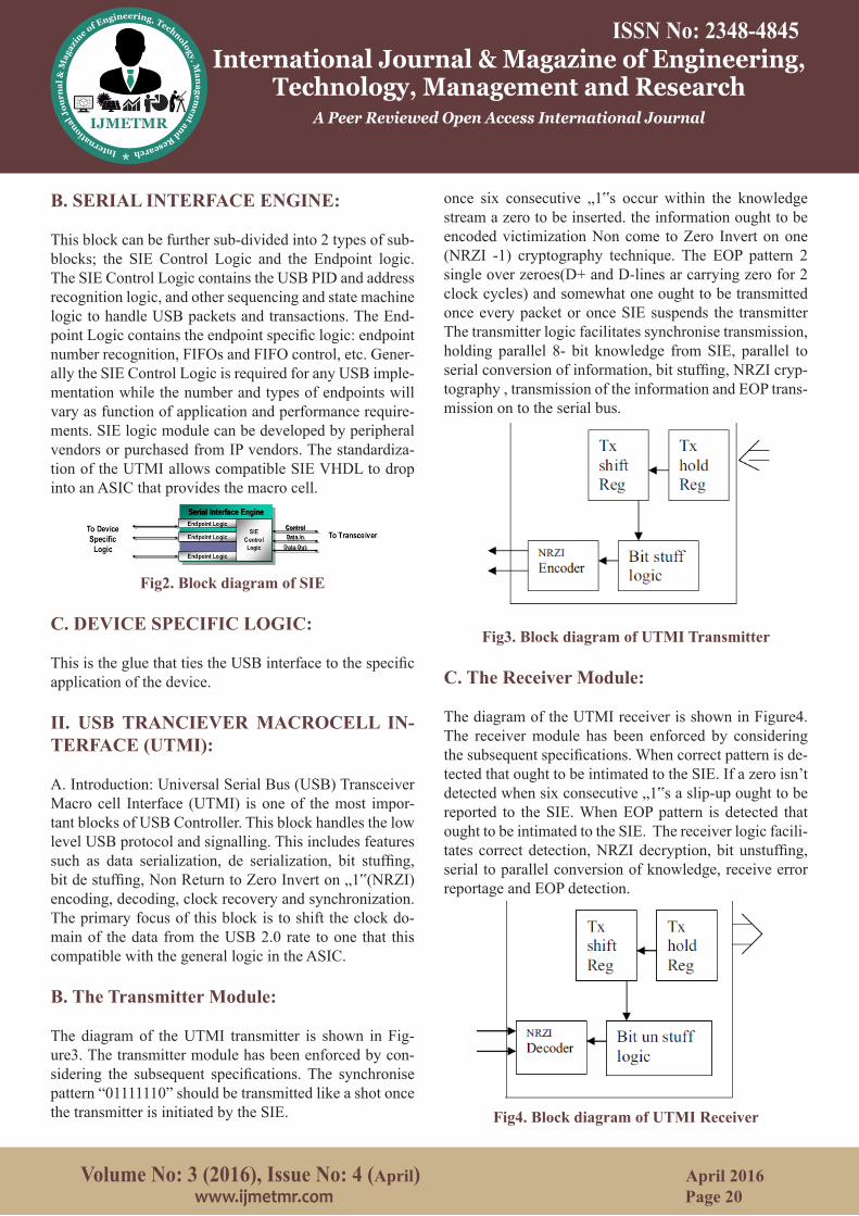
B. SERIAL INTERFACE ENGINE:
This block can be further sub-divided into 2 types of sub-blocks; the SIE Control Logic and the Endpoint logic. The SIE Control Logic contains the USB PID and address recognition logic, and other sequencing and state machine logic to handle USB packets and transactions. The End-point Logic contains the endpoint specific logic: endpoint number recognition, FIFOs and FIFO control, etc. Gener-ally the SIE Control Logic is required for any USB imple-mentation while the number and types of endpoints will vary as function of application and performance require-ments. SIE logic module can be developed by peripheral vendors or purchased from IP vendors. The standardiza-tion of the UTMI allows compatible SIE VHDL to drop into an ASIC that provides the macro cell.
Fig2. Block diagram of SIE
C. DEVICE SPECIFIC LOGIC:
This is the glue that ties the USB interface to the specific application of the device.
II. USB TRANCIEVER MACROCELL IN-TERFACE (UTMI):
A. Introduction: Universal Serial Bus (USB) Transceiver Macro cell Interface (UTMI) is one of the most impor-tant blocks of USB Controller. This block handles the low level USB protocol and signalling. This includes features such as data serialization, de serialization, bit stuffing, bit de stuffing, Non Return to Zero Invert on „1‟(NRZI) encoding, decoding, clock recovery and synchronization. The primary focus of this block is to shift the clock do-main of the data from the USB 2.0 rate to one that this compatible with the general logic in the ASIC.
B. The Transmitter Module:
The diagram of the UTMI transmitter is shown in Fig-ure3. The transmitter module has been enforced by con-sidering the subsequent specifications. The synchronise pattern “01111110” should be transmitted like a shot once the transmitter is initiated by the SIE.
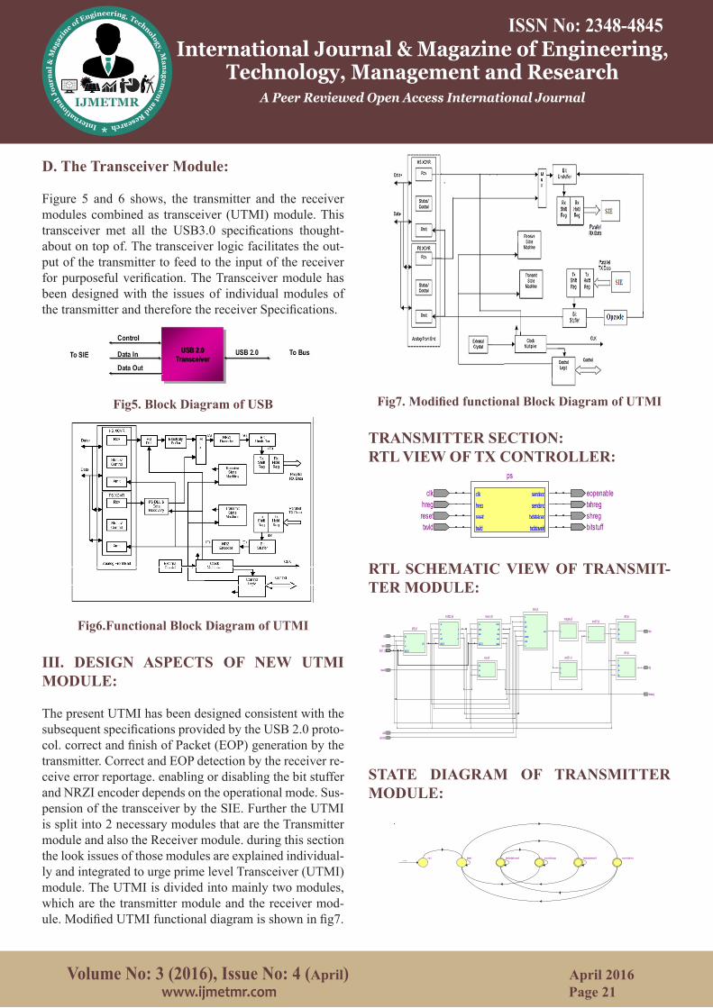
D. The Transceiver Module:
Figure 5 and 6 shows, the transmitter and the receiver modules combined as transceiver (UTMI) module. This transceiver met all the USB3.0 specifications thought-about on top of. The transceiver logic facilitates the out-put of the transmitter to feed to the input of the receiver for purposeful verification. The Transceiver module has been designed with the issues of individual modules of the transmitter and therefore the receiver Specifications.
Fig5. Block Diagram of USB
Fig6.Functional Block Diagram of UTMI
III. DESIGN ASPECTS OF NEW UTMI MODULE:
The present UTMI has been designed consistent with the subsequent specifications provided by the USB 2.0 proto-col. correct and finish of Packet (EOP) generation by the transmitter. Correct and EOP detection by the receiver re-ceive error reportage. enabling or disabling the bit stuffer and NRZI encoder depends on the operational mode. Sus-pension of the transceiver by the SIE. Further the UTMI is split into 2 necessary modules that are the Transmitter module and also the Receiver module. during this section the look issues of those modules are explained individual-ly and integrated to urge prime level Transceiver (UTMI) module. The UTMI is divided into mainly two modules, which are the transmitter module and the receiver mod-ule. Modified UTMI functional diagram is shown in fig7.
once six consecutive „1‟s occur within the knowledge stream a zero to be inserted. the information ought to be encoded victimization Non come to Zero Invert on one (NRZI -1) cryptography technique. The EOP pattern 2 single over zeroes(D+ and D-lines ar carrying zero for 2 clock cycles) and somewhat one ought to be transmitted once every packet or once SIE suspends the transmitter The transmitter logic facilitates synchronise transmission, holding parallel 8- bit knowledge from SIE, parallel to serial conversion of information, bit stuffing, NRZI cryp-tography , transmission of the information and EOP trans-mission on to the serial bus.
Fig3. Block diagram of UTMI Transmitter
C. The Receiver Module:
The diagram of the UTMI receiver is shown in Figure4. The receiver module has been enforced by considering the subsequent specifications. When correct pattern is de-tected that ought to be intimated to the SIE. If a zero isn’t detected when six consecutive „1‟s a slip-up ought to be reported to the SIE. When EOP pattern is detected that ought to be intimated to the SIE. The receiver logic facili-tates correct detection, NRZI decryption, bit unstuffing, serial to parallel conversion of knowledge, receive error reportage and EOP detection.
Fig4. Block diagram of UTMI Receiver
Fig7. Modified functional Block Diagram of UTMI
TRANSMITTER SECTION:RTL VIEW OF TX CONTROLLER:
RTL SCHEMATIC VIEW OF TRANSMIT-TER MODULE:
STATE DIAGRAM OF TRANSMITTER MODULE:
Volume No: 3 (2016), Issue No: 4 (April) April 2016 www.ijmetmr.com Page 20
Volume No: 3 (2016), Issue No: 4 (April) April 2016 www.ijmetmr.com Page 21
ISSN No: 2348-4845 ISSN No: 2348-4845International Journal & Magazine of Engineering,
Technology, Management and ResearchA Peer Reviewed Open Access International Journal
International Journal & Magazine of Engineering, Technology, Management and Research
A Peer Reviewed Open Access International Journal
B. SERIAL INTERFACE ENGINE:
This block can be further sub-divided into 2 types of sub-blocks; the SIE Control Logic and the Endpoint logic. The SIE Control Logic contains the USB PID and address recognition logic, and other sequencing and state machine logic to handle USB packets and transactions. The End-point Logic contains the endpoint specific logic: endpoint number recognition, FIFOs and FIFO control, etc. Gener-ally the SIE Control Logic is required for any USB imple-mentation while the number and types of endpoints will vary as function of application and performance require-ments. SIE logic module can be developed by peripheral vendors or purchased from IP vendors. The standardiza-tion of the UTMI allows compatible SIE VHDL to drop into an ASIC that provides the macro cell.
Fig2. Block diagram of SIE
C. DEVICE SPECIFIC LOGIC:
This is the glue that ties the USB interface to the specific application of the device.
II. USB TRANCIEVER MACROCELL IN-TERFACE (UTMI):
A. Introduction: Universal Serial Bus (USB) Transceiver Macro cell Interface (UTMI) is one of the most impor-tant blocks of USB Controller. This block handles the low level USB protocol and signalling. This includes features such as data serialization, de serialization, bit stuffing, bit de stuffing, Non Return to Zero Invert on „1‟(NRZI) encoding, decoding, clock recovery and synchronization. The primary focus of this block is to shift the clock do-main of the data from the USB 2.0 rate to one that this compatible with the general logic in the ASIC.
B. The Transmitter Module:
The diagram of the UTMI transmitter is shown in Fig-ure3. The transmitter module has been enforced by con-sidering the subsequent specifications. The synchronise pattern “01111110” should be transmitted like a shot once the transmitter is initiated by the SIE.
D. The Transceiver Module:
Figure 5 and 6 shows, the transmitter and the receiver modules combined as transceiver (UTMI) module. This transceiver met all the USB3.0 specifications thought-about on top of. The transceiver logic facilitates the out-put of the transmitter to feed to the input of the receiver for purposeful verification. The Transceiver module has been designed with the issues of individual modules of the transmitter and therefore the receiver Specifications.
Fig5. Block Diagram of USB
Fig6.Functional Block Diagram of UTMI
III. DESIGN ASPECTS OF NEW UTMI MODULE:
The present UTMI has been designed consistent with the subsequent specifications provided by the USB 2.0 proto-col. correct and finish of Packet (EOP) generation by the transmitter. Correct and EOP detection by the receiver re-ceive error reportage. enabling or disabling the bit stuffer and NRZI encoder depends on the operational mode. Sus-pension of the transceiver by the SIE. Further the UTMI is split into 2 necessary modules that are the Transmitter module and also the Receiver module. during this section the look issues of those modules are explained individual-ly and integrated to urge prime level Transceiver (UTMI) module. The UTMI is divided into mainly two modules, which are the transmitter module and the receiver mod-ule. Modified UTMI functional diagram is shown in fig7.
once six consecutive „1‟s occur within the knowledge stream a zero to be inserted. the information ought to be encoded victimization Non come to Zero Invert on one (NRZI -1) cryptography technique. The EOP pattern 2 single over zeroes(D+ and D-lines ar carrying zero for 2 clock cycles) and somewhat one ought to be transmitted once every packet or once SIE suspends the transmitter The transmitter logic facilitates synchronise transmission, holding parallel 8- bit knowledge from SIE, parallel to serial conversion of information, bit stuffing, NRZI cryp-tography , transmission of the information and EOP trans-mission on to the serial bus.
Fig3. Block diagram of UTMI Transmitter
C. The Receiver Module:
The diagram of the UTMI receiver is shown in Figure4. The receiver module has been enforced by considering the subsequent specifications. When correct pattern is de-tected that ought to be intimated to the SIE. If a zero isn’t detected when six consecutive „1‟s a slip-up ought to be reported to the SIE. When EOP pattern is detected that ought to be intimated to the SIE. The receiver logic facili-tates correct detection, NRZI decryption, bit unstuffing, serial to parallel conversion of knowledge, receive error reportage and EOP detection.
Fig4. Block diagram of UTMI Receiver
Fig7. Modified functional Block Diagram of UTMI
TRANSMITTER SECTION:RTL VIEW OF TX CONTROLLER:
RTL SCHEMATIC VIEW OF TRANSMIT-TER MODULE:
STATE DIAGRAM OF TRANSMITTER MODULE:
Volume No: 3 (2016), Issue No: 4 (April) April 2016 www.ijmetmr.com Page 20
Volume No: 3 (2016), Issue No: 4 (April) April 2016 www.ijmetmr.com Page 21
clkhregresettxvld
sendeopsendsnc
txdataloadtxdatawaittxvld
reset
clkhreg txhreg
shregbitstuff
eopenable
ps
pq
l
pq
la y
clkdinrst
y
aclkdinrst
y
aclkdinrst
yclkprstdin[7..0]
y[7..0]
clkprstshiftdin[7..0]
yz
z1
aclkclk2dinopcoderesetz1
output
clkresettxvldzdin[7..0]
bitstufffshift
shregtxhregtxready
and21:y1
and21:y2notgate:y3
eop:y4df1:y5
df3:y6shift22:y8
bitst:y9
trans:y10
clk
clk2
txvalid
reset
opcode
txready
dp
dm
din[7..0]
dff2:y7
rst txwt txdataload sendeop txdatawait sendsncreset

ISSN No: 2348-4845 ISSN No: 2348-4845International Journal & Magazine of Engineering,
Technology, Management and ResearchA Peer Reviewed Open Access International Journal
International Journal & Magazine of Engineering, Technology, Management and Research
A Peer Reviewed Open Access International Journal
RTL SCHEMATIC VIEW OF BIT STUFF MODULE:
STATE DIAGRAM OF BIT STUFF MOD-ULE:
RECEIVER SECTION:RTL VIEW OF RECEIVER CONTROL-LER:
STATE DIAGRAM FOR RECEIVER:
RTL VIEW OF BIT UNSTUFFING MOD-ULE:
SIMULATION RESULT OF BIT STUFF MODULE:
RTL VIEW OF PARALLEL TO SERIEL
SIMULATION RESULT OF PARALLEL TO SERI-EL:
STATE DIAGRAM FOR BIT UNSTUFF-ING:
IV. RESULTS:
The individual modules of the UTMI are designed using VHDL as stated above and they are simulated within the Xilinx based Model Sim 6.0 environment.
TRANSMITTER SECTION:A. The Transmitter Module:
The Figure shows the Simulation results of UTMI trans-mitter.
SIMULATION RESULT OF TRANSMIT-TER:
RTL VIEW OF SERIEL TO PARALLEL
SIMULATION RESULT OF SERIEL TO PARAL-LEL
RECEIVER SECTION:B. The Receiver Module: The Figure shows the Simulation results of UTMI re-ceiver. once correct is detected rxactive is declared. the info gift on rxdp, rxdm lines is decoded, serial to parallel born-again and sent to the SIE through knowledge out bus by declarative rxvalid signal.
SIMULATION RESULT OF BIT UNSTUFF-ING:
Volume No: 3 (2016), Issue No: 4 (April) April 2016 www.ijmetmr.com Page 22
Volume No: 3 (2016), Issue No: 4 (April) April 2016 www.ijmetmr.com Page 23
ab
y
abs
y clkdinrst
yclkresettemp
y
and1:y1
mux1:y2
dff1:y3
din
clk
clk2reset output
bitstuff:y4

ISSN No: 2348-4845 ISSN No: 2348-4845International Journal & Magazine of Engineering,
Technology, Management and ResearchA Peer Reviewed Open Access International Journal
International Journal & Magazine of Engineering, Technology, Management and Research
A Peer Reviewed Open Access International Journal
RTL SCHEMATIC VIEW OF BIT STUFF MODULE:
STATE DIAGRAM OF BIT STUFF MOD-ULE:
RECEIVER SECTION:RTL VIEW OF RECEIVER CONTROL-LER:
STATE DIAGRAM FOR RECEIVER:
RTL VIEW OF BIT UNSTUFFING MOD-ULE:
SIMULATION RESULT OF BIT STUFF MODULE:
RTL VIEW OF PARALLEL TO SERIEL
SIMULATION RESULT OF PARALLEL TO SERI-EL:
STATE DIAGRAM FOR BIT UNSTUFF-ING:
IV. RESULTS:
The individual modules of the UTMI are designed using VHDL as stated above and they are simulated within the Xilinx based Model Sim 6.0 environment.
TRANSMITTER SECTION:A. The Transmitter Module:
The Figure shows the Simulation results of UTMI trans-mitter.
SIMULATION RESULT OF TRANSMIT-TER:
RTL VIEW OF SERIEL TO PARALLEL
SIMULATION RESULT OF SERIEL TO PARAL-LEL
RECEIVER SECTION:B. The Receiver Module: The Figure shows the Simulation results of UTMI re-ceiver. once correct is detected rxactive is declared. the info gift on rxdp, rxdm lines is decoded, serial to parallel born-again and sent to the SIE through knowledge out bus by declarative rxvalid signal.
SIMULATION RESULT OF BIT UNSTUFF-ING:
Volume No: 3 (2016), Issue No: 4 (April) April 2016 www.ijmetmr.com Page 22
Volume No: 3 (2016), Issue No: 4 (April) April 2016 www.ijmetmr.com Page 23
ISSN No: 2348-4845 ISSN No: 2348-4845International Journal & Magazine of Engineering,
Technology, Management and ResearchA Peer Reviewed Open Access International Journal
International Journal & Magazine of Engineering, Technology, Management and Research
A Peer Reviewed Open Access International Journal
VII. CONCLUSION:
From the above results it can be concluded that the indi-vidual modules of UTMI have been designed, verified functionally using VHDL simulator. The UTMI Transmit-ter is capable of converting parallel data into serial bits, performing bit stuffing. The UTMI Receiver is capable of performing bit unstuffing and converting serial bits into parallel data. The functional simulation has been successfully carried out. UTMI has been design by using VHDL code and simulate using Xilinx, model-sim. This module is implement by using quartus-II tools.
FUTURE SCOPE:
The UTMI has been implemented is 8-bit one, it can also be extended to 16- bit UTMI. It can also be designed to generate CRCs for control and data packets. If an SIE and Device specific logic are designed, the combination of UTMI, SIE and Device specific logic can be used as controller of a USB device.
ACKNOWLEDGMENT:
We express my deep sense of gratitude and thanks Chair-man sir Sri. Raghu Kalidindi, Dean Prof S. Veerabhad-raiah, Head of the Department Mr. K.Phaninder Vinay and Principal Dr. R.Kameswara Rao sir of Raghu Engi-neering College Visakhapatnam, India for giving us this opportunity to carry out my project work at highly es-teemed Organization.
REFERENCES:
[1]. USB 2.0 Specification, April 27, 2000 [2]. USB 2.0 Transceiver Macrocell Interface (UTMI) Specification, version 1.05, March 29, 2001 [3]. On-The-Go Supplement to the USB 2.0 Specifica-tion, revision 1.0, Dec 18, 2001 [4]. UTMI+ Specification, revision 0.9, February 21, 2003 [5]. VHDL With Example Douglas .L .Perry [6]. Data and Computer Communications by William Stallings [7]. Computer Networks by Andrew S. Tannenbaum [8]. www.opencore.org [9]. www.digitalcoredesign.org
Volume No: 3 (2016), Issue No: 4 (April) April 2016 www.ijmetmr.com Page 24
Volume No: 3 (2016), Issue No: 4 (April) April 2016 www.ijmetmr.com Page 25