NORTHEASTERN UNIVERSITY Thesis Title: Author: …ece.neu.edu/groups/rcl/theses/hyu-ms2003.pdf ·...
101
NORTHEASTERN UNIVERSITY Graduate School of Engineering Thesis Title: Memory Architecture for Data Intensive Image Processing Algorithms in Reconfigurable Hardware Author: Haiqian Yu Department: Electrical and Computer Engineering Approved for Thesis Requirement of the Master of Science Degree _______________________________ ___________________ Thesis Advisor: Prof. Miriam Leeser Date _______________________________ ___________________ Thesis Reader: Prof. Eric Miller Date _______________________________ ___________________ Thesis Reader: Prof. Jennifer Dy Date _______________________________ ___________________ Department Chair: Prof. Fabrizio Lombardi Date Graduate School Notified of Acceptance: _______________________________ ___________________ Director of the Graduate School Date
-
Upload
phungkhuong -
Category
Documents
-
view
218 -
download
3
Transcript of NORTHEASTERN UNIVERSITY Thesis Title: Author: …ece.neu.edu/groups/rcl/theses/hyu-ms2003.pdf ·...

NORTHEASTERN UNIVERSITY
Graduate School of Engineering
Thesis Title: Memory Architecture for Data Intensive Image Processing Algorithms in Reconfigurable Hardware
Author: Haiqian Yu
Department: Electrical and Computer Engineering
Approved for Thesis Requirement of the Master of Science Degree
_______________________________ ___________________ Thesis Advisor: Prof. Miriam Leeser Date _______________________________ ___________________ Thesis Reader: Prof. Eric Miller Date _______________________________ ___________________ Thesis Reader: Prof. Jennifer Dy Date _______________________________ ___________________ Department Chair: Prof. Fabrizio Lombardi Date Graduate School Notified of Acceptance: _______________________________ ___________________ Director of the Graduate School Date

NORTHEASTERN UNIVERSITY
Graduate School of Engineering
Thesis Title: Memory Architecture for Data Intensive Image Processing Algorithms in Reconfigurable Hardware
Author: Haiqian Yu
Department: Electrical and Computer Engineering
Approved for Thesis Requirement of the Master of Science Degree
_______________________________ ___________________ Thesis Advisor: Prof. Miriam Leeser Date _______________________________ ___________________ Thesis Reader: Prof. Eric Miller Date _______________________________ ___________________ Thesis Reader: Prof. Jennifer Dy Date _______________________________ ___________________ Department Chair: Prof. Fabrizio Lombardi Date Graduate School Notified of Acceptance: _______________________________ ___________________ Director of the Graduate School Date Copy Deposited in Library: _______________________________ ___________________ Reference Librarian Date

MEMORY ARCHITECTURE FOR DATA INTENSIVE IMAGE PROCESSING ALGORITHMS IN RECONFIGURABLE HARDWARE
A Thesis Presented
by
Haiqian Yu
to
The Department of Electrical and Computer Engineering
in partial fulfillment of the requirements
for the degree of
Master of Science
in
Electrical Engineering
in the field of
Electrical Engineering
Northeastern University
Boston, Massachusetts
August 2003

1
Acknowledgements
First, I would like to thank my advisor Prof. Miriam Leeser for her consistent
support and patient guidance throughout this project. I benefit a lot from Prof. Miriam
Leeser’s keen insight of complicated problems and her useful suggestions.
Many thanks should go to Mercury Computer Systems Inc., which initiated the
project and funded my research. During the past two years, they provided useful
information and constructive suggestions that is essential for this thesis.
I would also like to thank my colleagues from the Rapid Prototyping Group at
Northeastern University for creating encouraging and supportive academic atmosphere
that makes research work more enjoyable.
Thanks to Srdjan Coric for allowing me to use “Parallel-beam Filterd
Backprojection” section from his thesis.
A special thanks goes to my husband, my parents and my sisters for their
unconditional love and constant encouragement. Their true love has been and will be the
stimulus for my whole life.

2
Abstract
FPGA implementation is attractive for computationally-intensive applications due
to FPGA’s speed and flexibility. Many of these applications, including image processing,
are data-intensive at the same time. In most cases, off-chip memory banks have to be
used to store the large amounts of data. Memory architecture organization then becomes
critical for an optimized design since frequent memory accesses can result in long delays
and degrade the system performance. A two-stage memory access structure, which
utilizes locality of reference has proved to be a successful implementation. In this
research, we apply this structure to the backprojection application. The idea of this
expandable architecture can be generalized to apply to other data-intensive applications.
An adaptive module is used in our implementation to isolate the core design and
the memory interface. This extra module can greatly improve the re-use of the HDL code
when migrating the design to a different hardware platform. Our implementation results
show that the hardware system can work on different target FPGA computing boards
with only a little modification. Moreover, performance is not affected on our current
platform, we can achieve more than 100 times speedup over software implementation.

3
Contents
Acknowledgements........................................................................................................................................1
Abstract ..........................................................................................................................................................2
Contents .........................................................................................................................................................3
List of Figures ................................................................................................................................................5
List of Tables..................................................................................................................................................6
1 Introduction ................................................................................................................................................7
1.1 Thesis Outline........................................................................................................................................8
2 Background...............................................................................................................................................10
2.1 Algorithm Introduction........................................................................................................................10
2.1.1 Parallel-beam Filtered Backprojection .........................................................................................10
2.1.2 Adapted Algorithm with Hardware Considerations .....................................................................19
2.2 HDL Based FPGA Design Process .....................................................................................................20
2.2.1 Hardware Description Languages ................................................................................................20
2.2.2 FPGA Design Flow ......................................................................................................................22
2.2.3 FPGA Structure and On-chip Memory.........................................................................................23
2.3 Computing Boards...............................................................................................................................27
2.4 Related Work.......................................................................................................................................30
2.5 Summary .............................................................................................................................................33
3 Experiment setup......................................................................................................................................34
3.1 Bit-width Selection..............................................................................................................................34
3.2 Memory Architecture ..........................................................................................................................35
3.3 Simple Architecture.............................................................................................................................40
3.4 Advanced Architecture ........................................................................................................................43

4
3.4.1 WildStar .......................................................................................................................................44
3.4.2 FireBird ........................................................................................................................................45
3.5 Adaptive Module.................................................................................................................................48
The function of these three process is described below: ...........................................................................54
3.6 Summary .............................................................................................................................................55
4 Results and Performance .........................................................................................................................56
4.1 Results .................................................................................................................................................56
4.2 Performance ........................................................................................................................................58
4.3 Summary .............................................................................................................................................62
5 Conclusion and Future Work..................................................................................................................63
5.1 Conclusion...........................................................................................................................................63
5.2 Future Work ........................................................................................................................................64
Bibliography ................................................................................................................................................67
Appendix A ..................................................................................................................................................70

5
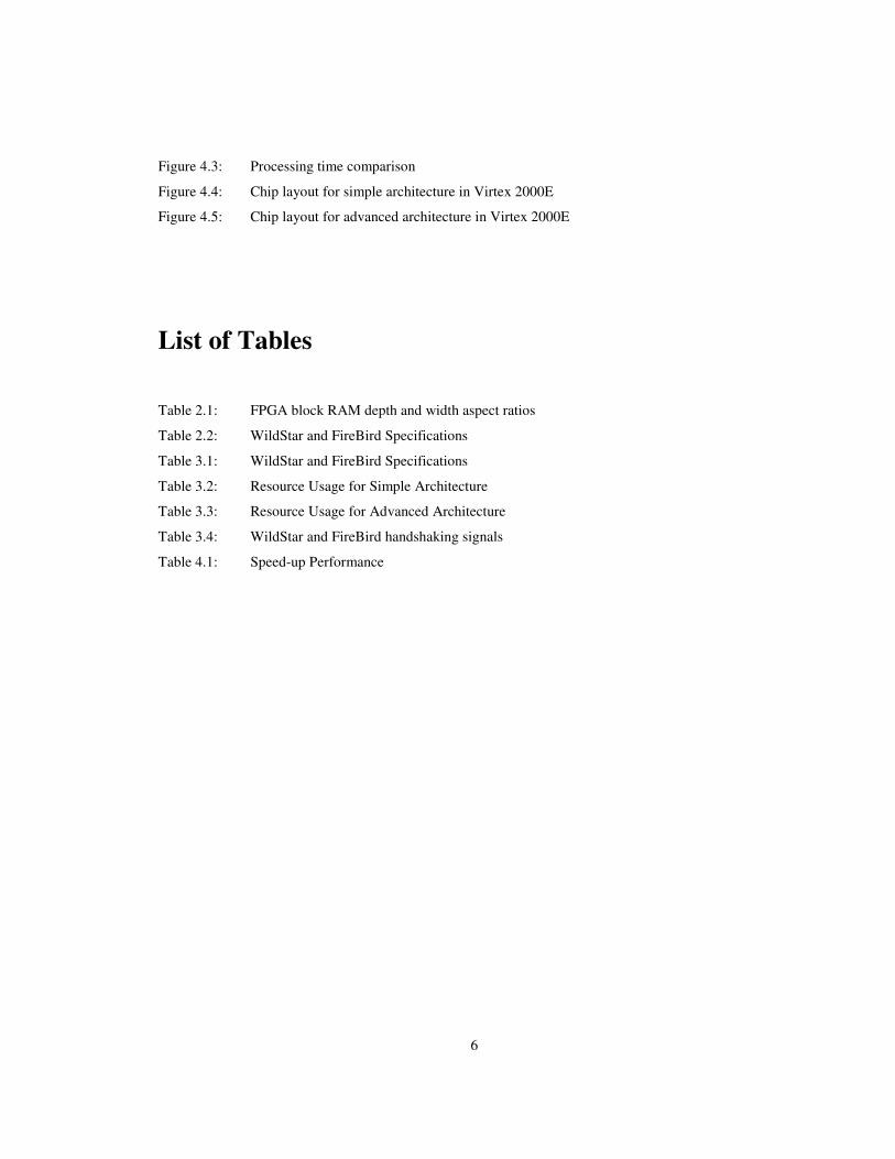
List of Figures
Figure 2.1: Illustration of the coordinate system used in parallel-beam backprojection
Figure 2.2: Reconstructions are often done using a procedure known as backprojection. Here a filtered
projection is smeared back over the reconstruction plane along lines of constant t. (From
[2].)
Figure 2.3: The ideal filter response for the filtered backprojection algorithm is shown here. It has been
bandlimited to 1/(2�). (From [2].)
Figure 2.4: The impulse response of the filter shown in Fig. 2.3 is shown here. (From [2].)
Figure 2.5: The DFT of the bandlimited filter (broken line) and that of the ideal filter solid line) are
shown here. Notice the primary difference is in the dc component. (From [2].)
Figure 2.6: HDL-based FPGA design flow
Figure 2.7: FPGA structure
Figure 2.8: 2-Slice Virtex CLB (From Xilinx, Inc.)
Figure 2.9: Detailed view of Virtex slice(From Xilinx, Inc.)
Figure 2.10: Annapolis WildStar (From Annapolis Micro Systems, Inc.)
Figure 2.11: Annapolis FireBird (From Annapolis Micro Systems, Inc.)
Figure 2.12: WildStar Schematic Diagram (From Annapolis Micro Systems, Inc.)
Figure 2.13: FireBird Schematic Diagram (From Annapolis Micro Systems, Inc.)
Figure 3.1: Typical memory read
Figure 3.2: Typical memory read-and-write
Figure 3.3: Data flow diagram in parallel-beam backprojection
Figure 3.4: Typical synchronized memory read
Figure 3.5: Typical synchronized memory write
Figure 3.6: Hardware Structure
Figure 3.7: Data format in off-chip memory
Figure 3.8: Parallel loading of 4 projections using two input
Figure 3.9: Parallel loading 14 projections using four input
Figure 3.10: Extending the loading time
Figure 3.11: Interface adaptive module
Figure 4.1: Reconstructed image comparison
Figure 4.2: Reconstructed image comparison, enlarged
6
Figure 4.3: Processing time comparison
Figure 4.4: Chip layout for simple architecture in Virtex 2000E
Figure 4.5: Chip layout for advanced architecture in Virtex 2000E
List of Tables
Table 2.1: FPGA block RAM depth and width aspect ratios
Table 2.2: WildStar and FireBird Specifications
Table 3.1: WildStar and FireBird Specifications
Table 3.2: Resource Usage for Simple Architecture
Table 3.3: Resource Usage for Advanced Architecture
Table 3.4: WildStar and FireBird handshaking signals
Table 4.1: Speed-up Performance
7
Chapter 1
Introduction
Computer images are extremely data intensive and hence require large amounts of
memory for storage. Image processing, in most cases, is data intensive as well as
computation intensive. To provide the horsepower necessary to process large amounts of
data in real-time, general-purpose DSP processors boards, application specific integrated
circuits (ASICs), multiprocessing systems and filed programmable gate arrays (FPGAs)
have been chosen to accelerate the processing time. Among all these methods,
reconfigurable devices are attractive due to their ability to be dynamically reconfigured
for different application and their inherent fine-grained parallelism. Moreover, FPGAs
provide a simpler design cycle than ASICs, which makes time to market shorter, and
have greater customization capabilities to make hardware more efficient than a software
solution.
Due to the limited memory resources and complexity of the routing architecture
[1] on the FPGA chip, external memory banks are necessary for most image processing
applications. This also means that part of the FPGA needs to be configured as an
interface to the external memory while the other part is configured to perform the
required image processing operation. In this thesis, we call these external memories off-
chip memory, in contrast with block RAMs inside FPGA chip, which is called on-chip

8
memory. Normally off-chip memory, although much larger, has slower reads/writes than
on-chip memory. Accelerating the processing time while utilizing the large storage space
of off-chip memory heavily depends on how we design the memory architecture. In this
thesis, using the parallel-beam backprojection algorithm [2] as an example, we discuss
FPGA memory architectures for data intensive image processing applications.
Another issue for hardware design is its re-use. Due to the off-chip memory
requirement, we have to design different memory interfaces for different target boards.
Synchronization between computation and memory read/write are critical for the
processing, thus some of the memory handshaking signals are used as control signals in
the design. If we change the target board, we may have to rewrite most of the VHDL
code. In this thesis, we present an adaptive module between the core design and the
memory interface that can maximally isolate the two parts. In this case, when we migrate
the design from one board to another, we only need to rewrite the adaptive module. This
can greatly increase the re-usability of the VHDL code and correspondingly, shorten the
time-to-market cycle.
1.1 Thesis Outline
This thesis is organized as follows:
Chapter 2 describes the algorithm of parallel-beam backprojection followed by a
brief review of the HDL-based FPGA design process. In this chapter, the FPGA

9
computing boards we used and their differences are also introduced. The final part gives
an overview of related work. Chapter 3 describes the detailed hardware implementation
process, specifically concentrating on the memory architecture design of both simple and
advanced architectures for our design. The use of the adaptive module is also introduced
in this chapter. Chapter 4 gives the results and analysis of the hardware design. The
performance of two different implementations are included in this chapter. Chapter 5
presents conclusion and gives suggestions for future work.

10
Chapter 2
Background
Before addressing the memory organization issues in this thesis, we give some
basic information on the parallel-beam backprojection algorithm. After that, a brief
overview of reconfigurable hardware in general and specifics of the platform used for
hardware implementation are described. Related work is also summarized in this chapter.
2.1 Algorithm Introduction
The most commonly used approach for image reconstruction from parallel-beam
projection data is filtered backprojection. The following sections introduce the detailed
algorithm and the corresponding hardware adapted algorithm. Most of this material has
been presented previously in [2,3,4].
2.1.1 Parallel-beam Filtered Backprojection
A parallel-beam CT scanning system uses an array of equally spaced
unidirectional sources of focused X-ray beams. Generated radiation, not absorbed by the
object’s internal structure, reaches a collinear array of detectors (Figure 2.1). Spatial

11
variation of the absorbed energy in the two-dimensional plane through the object is
expressed by the attenuation coefficient f(x, y). The logarithm of the measured radiation
intensity is proportional to the integral of the attenuation coefficient along the straight
line traversed by the X-ray beam. A set of values given by all detectors in the array
comprises a one-dimensional projection of the attenuation coefficient, P(t, �), where t is
the detector distance from the origin of the array, and � is the angle at which the
measurement is taken. A collection of projections for different angles over 180° can be
visualized in the form of an image in which one axis is position t and the other is angle �.
Figure 2.1: Illustration of the coordinate system used in parallel-beam backprojection

12
This is called a sinogram or Radon transform of the two-dimensional function f, and it
contains information needed for the reconstruction of an image f(x, y). The Radon
transform can be formulated as
( ) ( ) ( ) , , sincos ,log 0 θθθδ tPdydxtyxyxfII
de ≡−+= �� (2.1)
where Io is the source intensity, Id is the detected intensity, and �(·) is the Dirac
delta function. Equation (2.1) is actually a line integral along the path of the X-ray beam,
which is perpendicular to the t axis (see Figure 2.1) at location t = xcos � + ysin �. The
Radon transform represents an operator that maps an image f(x, y) to a sinogram P(t, �).
Its inverse mapping, called the inverse Radon transform, applied to a sinogram results in
an image. The filtered backprojection (FBP) algorithm performs this mapping [2].
The mathematical derivation of the filtered backprojection algorithm for parallel-
beam projections is summarized and presented in [3]. Here we directly give the final
conclustion.
)sin cos( ) ,(�
0
θθθθ dyxQyxf � += (2.2)
where
. )()( �2 dwewwStQ wtj�∞
∞−
= θθ (2.3)
This estimate of f(x, y), given the projection data transform S�(w), has a simple
form. Equation (2. 3) represents a filtering operation, where the frequency response of

13
the filter is given by | w |; therefore Q�(t) is called a “filtered projection.” The resulting
projections for different angles � are then added to form the estimate of f(x, y).
Equation (2.2) calls for each filtered projection, Q�, to be “backprojected.” This
can be explained as follows. To every point (x, y) in the image plane there corresponds a
value of t = x cos � + y sin � for a given value of �, and the filtered projection Q�
contributes to the reconstruction of its value at t (= x cos � + y sin �).
Figure 2.2: Reconstructions are often done using a procedure known as backprojection. Here a filtered projection is smeared back over the
reconstruction plane along lines of constant t. (From [2].)
This is further illustrated in Fig. 2.2. It is easily shown that for the indicated angle
�, the value of t is the same for all (x, y) on the line LM. Therefore, the filtered
projection, Q�, will make the same contribution to the reconstruction at all of these
14
points. Therefore, one could say that in the reconstruction process each filtered
projection, Q�, is smeared back, or backprojected, over the image plane.
The parameter w has the dimension of spatial frequency. The integration in (2.3)
must, in principle, be carried out over all spatial frequencies. In practice the energy
contained in the Fourier transform components above a certain frequency is negligible, so
for all practical purposes the projections may be considered to be band-limited. If W is a
frequency higher than the highest frequency component in each projection, then by the
sampling theorem the projections can be sampled at intervals of
WT
21= (2.4)
without introducing any error. If we also assume that the projection data are equal to
zero for large values of | t | then a projection can be represented as
12
, . . . ,0 , . . . ,2
),( −−= NNmmTPθ (2.5)
for some (large) value of N.
Assume that the projection data are sampled with a sampling interval of � cm. If
there is no aliasing, then in the transform domain the projections don’t contain any
energy outside the frequency interval (- W, W) where
cycles/cm. 21τ
=W (2.6)
Let the sampled projections be represented by P�(k�) where k takes integer values.
The theory presented in the preceding subsection says that for each sampled projection

15
P�(k�) we must generate a filtered Q�(k�). When the highest frequency in the projections
is finite (as given by Eq. (2.6)), Eq. (2.3) may be expressed as
dwewHwStQ wtj�∞
∞−
= )()()( �2θθ (2.7)
where
)( )( wbwwH w= (2.8)
where, again,
��� <
=. otherwise
01
)(Ww
wbw (2.9)
H(w), shown in Fig. 2.3, represents the transfer function of a filter with which the
projections must be processed. The impulse response, h(t), of this filter is given by the
inverse Fourier transform of H(w) and is
2
22
�2
2/ �2/ �sin
4
12/ �2
2/ �2sin
2
1
)()(
��
��
−=
= �∞
∞−
ττ
τττ
τ tt
tt
dwewHth wtj
(2.10)
where we have used Eq. (2.6). Since the projection data are measured with a
sampling interval of �, for digital processing the impulse response need only be known
with the same sampling interval. The samples, h(n �), of h(t) are given by

16
odd n
even n
0n
�
1,0
,41
)(
222
2 =
��
�
��
�
�
−
=
τ
ττ
n
nh (2.11)
This function is shown in Fig. 2.4.
Figure 2.3: The ideal filter response for the filtered backprojection algorithm is shown here. It has been bandlimited to 1/(2�). (From [2].)
By the convolution theorem the filtered projection at the sampling points can be
written as
. )( ) ()( τττττ θθ kPknhnQk�∞
−∞=−= (2.12)

17
In practice each projection is of only finite extent. Suppose that each P�(k�) is
zero outside the index range k = 0, . . ., N - 1. We may now write the following two
equivalent forms of Eq. (2.12):
, )( ) ()(1
0
τττττ θθ kPknhnQN
k�
−
=−= n=0, 1, 2, . . ., N-1 (2.13)
or , )( ) ()(1
)1(
τττττ θθ knPkhnQN
Nk
−= �−
−−= n=0, 1, 2, . . ., N-1 (2.14)
Figure 2.4: The impulse response of the filter shown in Fig. 2.3 is shown here. (From [2].)
18
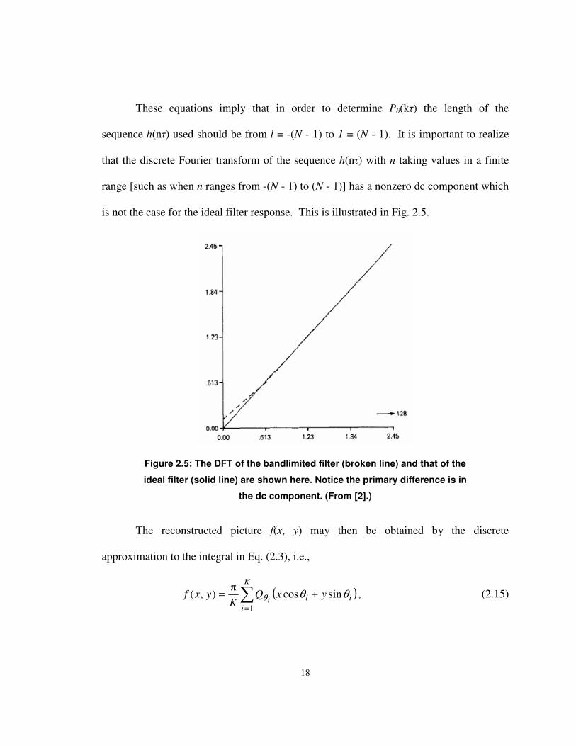
These equations imply that in order to determine P�(k�) the length of the
sequence h(n�) used should be from l = -(N - 1) to 1 = (N - 1). It is important to realize
that the discrete Fourier transform of the sequence h(n�) with n taking values in a finite
range [such as when n ranges from -(N - 1) to (N - 1)] has a nonzero dc component which
is not the case for the ideal filter response. This is illustrated in Fig. 2.5.
Figure 2.5: The DFT of the bandlimited filter (broken line) and that of the
ideal filter (solid line) are shown here. Notice the primary difference is in
the dc component. (From [2].)
The reconstructed picture f(x, y) may then be obtained by the discrete
approximation to the integral in Eq. (2.3), i.e.,
( ) , sin cos�
) ,(1
ii
K
i
yxQK
yxfi
θθθ += �=
(2.15)
19
where the K angles �i are those for which the projections P�(t) are known. Note
that the value of x cos �i + y sin �i in Eq. (2.15) may not correspond to one of the k� at
which i
Qθ is known. However, i
Qθ for such t may be approximated by suitable
interpolation; often, linear interpolation is adequate.
2.1.2 Adapted Algorithm with Hardware Considerations
For the practical implementation of filtered parallel-beam backprojection, it is
important to determine how many projections and how many samples per projection one
should use to obtain a highly accurate reconstruction. The values [3] used for our
implementation, are: the reconstructed image size is 512*512, the number of projections
is 1024, each projection has 1024 samples. We also assume square pixels and use the
look-up tables (LUTs) and incremental spatial address calculation as suggested in [4].
Basically, equation (2.15) can be summarized as follows: For each pixel of the
reconstructed image, we should find the sinogram data that contributes to this pixel for
the current projection and accumulate the value for all the projections.
According to the image size and sinogram size we select, the input of the design
would be the 1024*1024 sinogram data and the output is the 512*512 reconstructed
image. To get the output, the computation would be 512*512*1024 since reconstruction
is an accumulation process through 1024 projections for each pixel. Clearly, this is both a
computation-intensive and memory-intensive algorithm. For software calculation, it takes
20
minutes to hours for one image reconstruction depending on the software and the
algorithm. Our fastest software implementation needs 28 seconds, which is too slow for
real-time applications. That is one of the reasons why we designed a hardware
implementation for acceleration. Xilinx FPGA chips are our target technology due to
their flexibility and processing speed. However, using current technology, it is impossible
to load all the input data or output data to any FPGA for computation. That means we
have to use some external memory banks with interfaces to the FPGA chip to store the
input and output data. For maximum performance, we have to carefully design the
memory architecture, fully utilizing the pipelined structure and parallelism of the design.
2.2 HDL Based FPGA Design Process
2.2.1 Hardware Description Languages
HDLs provide formats for representing various design stages. They are used to
describe hardware for the purpose of simulation, modeling, testing, design, and
documentation. These languages provide a convenient and compact format for the
hierarchical representation of functional and wiring details of digital systems. There are
several levels of abstraction of digital systems using hardware description languages.

21
A Behavioral description is the most abstract. It describes the function of the
design in a software-like procedural form and provides no detail as to how the design is
to be implemented. Behavioral descriptions are necessary in the early design stage so that
simulations can ensure that the chip is functionally correct. The advantage of this
approach is that we can make this assessment independent of the many possible physical
implementations.
A dataflow description is a concurrent representation of the flow of control and
movement of data. It gives more detail of hardware implementation and shows how data
moves between registers.
A structural description is the lowest and most detailed level of description
considered here and is the simplest to synthesize into hardware.
Available software for HDLs includes simulators and hardware synthesis
programs. A simulation program can be used for design verification, while a synthesizer
is used for automatic hardware generation. Moreover, synthesizers can be divided into
two parts, high level synthesizer and low level synthesizer. The high level synthesizer can
transform behavioral description HDL into structural description HDL, which includes
some primitive components, generally gates, flip-flops and latches. The low level
synthesizer depends on the target hardware and its main tasks are place & route and
optimization. In some papers and books, this process is called hardware implementation
since the output of the low level synthesizer directly maps to the primitives that are used
in the target chip.

22
2.2.2 FPGA Design Flow
Typically, the HDL-based FPGA design flow has three steps:
1. Use VHDL or Verilog to describe digital systems; a simulation tool is required to
simulate and verify the design.
2. Use RTL (Register Transfer Level) synthesis tool to obtain structure level design.
3. Use FPGA placement & routing tools to obtain physical FPGA netlist.
Simulation/Verification(ModelSim)
Synthesis(Synplicity)
Optimize, place&route(Xilinx ISE)
Design EntryVHDL
Structure-level designEDF file
Constraint not met
BitstreamDownload
FPGA computing board
Figure 2.6 HDL-based FPGA design flow

23
Specifically, our FPGA design flow is shown in Figure 2.6.
ModelSim, Synplify and Xilinx ISE are the tools we used for simulation,
synthesis and implementation respectively. The final bit-stream is downloaded to the
FPGA computing board through a host PC. We check the output of our implementation
for function verification. If the result is not correct, then we will go through the three
steps again until we get the final successful design. The following section explains why
we are using FPGA computing boards.
2.2.3 FPGA Structure and On-chip Memory
The key to the popularity of FPGAs is their ability to implement any circuit
simply by being appropriately programmed. Other circuit implementation options, such
as Standard Cells or Mask-Programmed Gate Arrays (MPGAs), require that a different
VLSI chip be newly fabricated for each design. The use of a standard FPGA, rather than
these custom technologies, has two key benefits: lower non-recurring engineering (NRE)
costs, and faster time-to-market.
All FPGAs are composed of three fundamental components: logic blocks, I/O
blocks and programmable routing, as Figure 2.7 shows. A circuit is implemented in an
FPGA by programming each of the logic blocks to implement a small portion of the logic
required by the circuit, and each of the I/O blocks to act as either an input pad or an
output pad, as required by the circuit. The programmable routing is configured to make

24
all the necessary connections between logic blocks and from logic blocks to I/O
blocks[1].
Figure 2.8 2-Slice Virtex CLB (From Xilinx, Inc.)
Logic blockI/O block
Programmablerouting
Figure 2.7 FPGA structure

25
The logic block used in most modern FPGAs are composed of groups of Look-Up
Tables and registers with some local interconnect between them. The FPGA chips we use
are Xilinx Virtex series. Virtex devices provide better performance than previous
generations of Xilinx FPGAs. Designs can achieve synchronous system clock rates up to
200MHz including I/O. Moreover, Virtex FPGAs incorporate several large block RAM
memories. These complement the shallow RAM structures implemented in CLBs. For the
Virtex series, each CLB contains four logic cells (LCs), organized in two similar slices,
as shown in Figure 2.8. Figure 2.9 shows a more detailed view in a single slice [5,6].
These LUTs can either be combined or used separately to implement any logical
function.
Figure 2.9 Detailed view of Virtex slice(From Xilinx, Inc.)

26
As we have mentioned before, FPGAs have two key benefits: lower non-recurring
engineering (NRE) costs, and faster time-to-market. These two benefits make FPGAs one
of the most popular implementation media for digital circuits.
Due to the memory requirement of most applications, most current FPGA chips,
such as the Virtex, Spartan-3 and Virtex-II series, have several block RAMs inside the
chips. We are interested in Virtex series since they are the FPGA chips we used currently.
The following discussion about block RAMs are specific to Virtex series unless
specified. Block RAMs are organized in columns and the number of block RAMs
depends on the FPGA you choose. Each block RAM contains 4096 memory cells and
provide true dual-read/write port synchronous RAM. Each port of the block RAM
memory can be independently configured as a read/write port, a read port, or a write port;
and each port can be configured to a specific data width such as 1,2,4,8…. That means if
you use block RAM to store your 9 bit data, one block RAM can only store 256 data
items since it has to select the 16-bit data width for storage. However, several block
RAMs can be combined together to achieve wider and deeper RAM structures. Table 2.1
describes the depth and width aspect ratios for the block RAM. Another advantage of on-
chip RAM is its short response time. Users can read/write data in one clock cycle.
For applications like image processing, which require a very large memory to
store the data, it is impossible to load all the data into the FPGA block RAM due to its
area and routing limitations. In our case, the input data is 1024*1024*9bit ≅ 1.1Mbyte,
while the block RAMs in FPGA holds up to several hundred Kbytes.

27
Table 2.1 FPGA block RAM depth and width aspect ratios
Width Depth ADDR Bus Data Bus
1 4096 ADDR<11:0> DATA<0>
2 2048 ADDR<10:0> DATA<1:0>
4 1024 ADDR<9:0> DATA<3:0>
8 512 ADDR<8:0> DATA<7:0>
16 256 ADDR<7:0> DATA<15:0>
2.3 Computing Boards
One of the biggest advantages of applying hardware designs to an FPGA is the
possibility for really fast prototyping. However, although the turn around time from
VHDL description to FPGA floorplan is short, the last step from having the floorplan to a
working design in hardware can require an unintended percentage of the designers time
schedule. The problem is that although the FPGA can function almost as a stand-alone
unit; peripheral components, such as static memory and communication equipment
usually have to be wired to the FPGA before such architectures can be verified. That is
why we are using Annapolis Micro Systems’ computing boards for our implementation.
WildStar and FireBird [7,8] are two computing FPGA boards, which not only have large

28
off-chip memory storage, but also have PCI controllers. They make the data transfer
between PC and the computing board very convenient. The manufacturer also provides
user supplied interface code specific to the memory types, which define the handshaking
signals between FPGA chip and memories. Users only need to use these signals to
control the data exchange.
WildStar and FireBird’s specifications are listed in Table 2.2:
Table 2.2 WildStar and FireBird Specifications
WildStar FireBird
� 3 Xilinx® VIRTEX™ 1000 FPGAs with 3
million system gates
� 1 VirtexTM E FPGA Processing Element -
XCV2000E, that is 2 million gates
� Processing clock rates up to 100MHz � Processing clock rates up to 150MHz
� 1.6 GB/s I/O bandwidth � 4.2 GB/s I/O bandwidth
� 6.4 GB/s memory bandwidth � 6.6 GB/s memory bandwidth
� 40MB of 100MHz Synchronous ZBT SRAM � 30MB of 150MHz Synchronous ZBT SRAM
The pictures of these two boards and their schematic diagrams of the boards are
shown in the following figures.
Figure 2.10: Annapolis WildStar (From Annapolis Micro Systems, Inc.)

29
Figure 2.11: Annapolis FireBird (From Annapolis Micro Systems, Inc.)
PCI/VMEBridge
PCIArbiter
PCIController
ClkCrossbar
MEM0
MEM1
RIGHT PE1 MEZZ CONN
64 bits 64 bits
VME 64X PCI Local Bus 64 bits
CPU Card
PE 1 PE 0 PE 2I/O
Card0
I/OCard
1
Local Address/Data 32 Bits 33 MHz
Bottom Systolic Bus 36 bits
Crossbar
MEM0
MEM1
RIGHT PE2 MEZZ CONN
64 bits 64 bits
Crossbar
MEM0
MEM1
LEFT PE1 MEZZ CONN
64 bits 64 bits
Top Systolic Bus 36 bits
Crossbar
MEM0
MEM1
64 bits 64 bits
LEFT PE2 MEZZ CONN
LEFTMEM
LEFTMEM
32 bits
32 bits
LEFTMEM
LEFTMEM
32 bits
32 bits64 bits 64 bits
32 bits 32 bits
32 bits 32 bits64 bits 64 bits
64 bits 64 bits
Figure 2.12: WildStar Schematic Diagram (From Annapolis Micro Systems, Inc.)

30
We have to divide the FPGA design into two parts; one is the processing part,
which takes the data and does the processing, and the other is the memory interface,
which reads/writes data from/to the memory. For memory-intensive designs like parallel-
beam backprojection, we have to carefully organize the memory architecture for fast and
efficient data exchange.
2.4 Related Work
In previous work in the area of hardware implementations of tomographic
processing algorithms, Wu[9] gives a brief overview of all major subsystems in a
computed tomography (CT) scanner and proposes locations where ASICs and FPGAs
can be utilized. According to the author’s discussion, semi-custom digital ASICs were the
PCIConnector
CLK
PCIController
Flash
VIRTEXTMEXCVE2000
Mem_0ZBT SRAM
8MB
PCI Bus(64 bits)
LAD Bus
66MHz, 64 bits
64 b
its
64 b
its
32 b
its
64 b
its
64 b
its
Mem_1ZBT SRAM
8MB
Mem_2ZBT SRAM
8MB
Mem_3ZBT SRAM
8MB
Mem_4ZBT SRAM
4 MB
Figure 2.13: FireBird Schematic Diagram (From Annapolis Micro Systems, Inc.)

31
most appropriate due to the level of sophistication that FPGA technology had in 1991.
Agi et. al.[10] present the first description of a hardware solution for computerized
tomography of which we are aware. It is a unified architecture that implements forward
Radon transform, parallel- and fan-beam backprojection in an ASIC based multi-
processor system. Our FPGA implementation focuses on backprojection. Agi et al. [11]
present a similar investigation of quantization effects; however their results do not
demonstrate the suitability of their implementation for medical applications. Although
their filtered sinogram data are quantized with 12-bit precision, extensive bit truncation
on functional unit outputs and low accuracy of the interpolation factor (absolute error of
up to 2) render this implementation significantly less accurate than ours, which is based
on 9-bit projections and the maximal interpolation factor absolute error of 2-4. An
alternative to using specially designed processors for the implementation of filtered
backprojection (FBP) is presented in [12]. In this work, a fast and direct FBP algorithm is
implemented using texture-mapping hardware. It can perform parallel-beam
backprojection of a 512-by-512-pixel image from 804 projections in 2.1 seconds, while
our implementation takes 0.25 seconds from 1024 projections. Luiz et. al.[13]
investigated residue number systems (RNS) for the implementation of convolution based
backprojection to speedup the processing. Unfortunately, extra binary-to-RNS and RNS-
to-binary conversions are introduced. Approaches to accelerating the backprojection
algorithm can be found in [14,15]. However, their suitability to medical image quality
and hardware implementation are still under investigation. Bins et. al.[16] have

32
investigated precision vs. error in JPEG compression. The goals of this research are very
similar to ours: to implement designs in fixed-point in order to maximize parallelism and
area utilization. However, JPEG compression is an application that can tolerate a great
deal more error than medical imaging.
In this thesis, we focus on FPGA implementation performance and medical image
quality as well as the memory structure design for data-intensive applications. Filtered
Back-Projection (FBP) is a computationally and data intensive process. For an image of
size n × n being reconstructed with n projections, the complexity of the backprojection
algorithm is O(n3). The input data is n2 and the output data is also n2. Moreover, a
difficulty of implementing FBP is that producing high-resolution images with good
resemblance to internal characteristics of the scanned object requires that both the density
of each projection and their total number be large. This represents a considerable
challenge for hardware implementations, which attempt to maximize the parallelism in
the implementation. Therefore, it can be beneficial to use fixed-point implementations
and to optimize the bit-width of a projection sample to the specific needs of the targeted
application domain. In a previous thesis[3,4], the author presents a detailed hardware
architecture based on software simulation results and successfully implements this
application. Our FPGA design is based on these results [3,4] and pays more attention to
the memory architecture organization.
Notably, problems arise when we migrating the backprojection design from one
board to another. Ideally, once we get a successful HDL version of an FPGA design, we

33
expect it to work properly on other platforms without many modifications. Unfortunately,
this seldom is the case for designs with interfaces to off-chip memories and/or I/O ports.
Changes to the memory organization or board design may result in the designer having to
rewrite most of the HDL code. This is the case when we migrated the memory-intensive
design, parallel-beam backprojection, from the WildStar to FireBird boards from
Annapolis Microsystems [7,8].
A lot of attention has been paid to building general-purpose memory interfaces to
interact with external memory. Most of them aim at multi-processor FPGA systems
[17,18] and are concerned with memory access conflict issues. For memory-intensive
single processor FPGA designs with a vendor-specific HDL interface, we are more
interested in a portable design with maximally re-use of the existing HDL code. Not
much work has been done in this area.
2.5 Summary
This chapter gives the general background to the backprojection algorithm and the
FPGA implementation of this algorithm. Our design entry and the design process are also
introduced in this chapter. We emphasize on the on-chip and off-chip memory. Related
work is also included here. We will discuss the memory issue in the next chapter.

34
Chapter 3
Experiment setup
The most important reason for hardware implementation is its higher processing
speed. Fixed-point and pipelined structures are used in our implementation for speed-up.
For an application with frequent memory accesses, a two-stage memory architecture is
designed for further speed-up. Moreover, to maximize the re-use of our HDL-based
design, we introduced an adaptive module in this thesis. This chapter gives the details of
all these techniques we used in our design.
3.1 Bit-width Selection
Unlike software computation, in hardware implementation fixed-point is preferred
for its compact size and fast speed. Hardware size and speed are two primary factors for a
high performance system. Smaller size means lower cost while higher speed means less
processing time. When implementing an algorithm or application in hardware, normally
we want to maximize the processing performance and keep the cost under some specified
limit. For medical imaging, we have to take one more thing into consideration: accuracy.

35
Specifically, care must be taken so that very little error is introduced compared to
floating-point implementations and the visual quality of the image is not compromised.
That means when we reduce the bit-width to decrease the hardware size, we have to make
sure the quality of the reconstructed image is comparable to the floating-point
reconstruction. It is very important to balance area and accuracy. Larger bit width
corresponds to more accuracy but also more area and lower speed. Moreover, we need to
investigate for each stage of the design whether it is feasible to disregard some of the
least significant bits (LSBs) and still not introduce any visible error.
According to simulation results from [3], which investigates the quantization
effect for each stage of reconstruction, we use 9 bits for sinogram quantization and 3 bits
for linear interpolation. Since disregarding LSBs won’t save much hardware area, we
preserve the LSBs for intermediate results at each stage. Pipelined structures are used for
higher throughput.
3.2 Memory Architecture
As we have mentioned in the algorithm introduction, we reconstruct the image
once for each projection and accumulate the results for all the projections. For each pixel,
we need to find the address of the corresponding sinogram data that contributes to this
pixel. We can’t predict the address of the sinogram for the next pixel since it varies from

36
pixel to pixel, line to line, projection to projection. This is the issue: although we can
easily access the on-chip memory in one clock cycle, the size of the on-chip memory is
too small to store all the sinogram data. But if all the data are stored in off-chip memory,
when the address is generated, we must send a read request to the memory, then wait for
the data to be ready to read, which may take several cycles. In this case, even if we
already have the next address, we can’t get the data for several cycles. A typical memory
read waveform is shown in Figure 3.1.
There is also not enough space for the reconstructed image in the on-chip
CLK
Slect_Memory
Address
Data_valid
Data
Read
A0
D0
Figure 3.1: Typical memory read
CLK
Slect_Memory
Address
Data_valid
Data_read
Read
A0
D0
Data_write D1
A0
Write
Figure 3.2: Typical memory read-and-write

37
memory. For each projection, each pixel should be updated. That means it needs to be
read in, the new value needs to be added and then the pixel should be stored back to the
off-chip memory. This is a typical read-and-write cycle; its waveform is shown in Figure
3.2.
Clearly, if we want to update the image, we have to wait several clocks for each
pixel. For example, if the number of clock cycles to wait for a read is 2, then for one
projection, 512*512*2 clock cycles are wasted. For a processing frequency of 50MHz,
the overall reconstruction will at least waste 512*512*2*1024*(1/50,000,000) =
10.737seconds. This will severely degrade performance.
In summary, if all the data are store in off-chip memory, we will waste a lot of
time waiting for the data. On-chip memory has a much faster read/write cycle, but it
cannot accommodate all the data. To solve this problem, we use a memory hierarchy
structure in our design by exploiting the spatial locality of input data of the algorithm.
We already know that the sinogram address for the next pixel can not be
determined by the current address, but if we have all the sinogram data for this projection
stored in the block RAM, then we can always get the data no matter what the address is.
That is spatial locality, which means that although we don’t know which sinogram data
will be selected for the next pixel, we do know it must be some of the data in the current
projection. Based on this fact, we have the data flow shown in Figure 3.3.

38
All the sinogram data for the first projection are pre-loaded to the on-chip
memory. Once it is loaded, the sinogram data address generation (SAG) module starts to
work. For each pixel to be reconstructed, the SAG finds out which sinogram value
corresponds to this pixel for this projection. Linear interpolation is used in case the
address is not an integer. All the calculations are pipelined for speedup. While the SAG is
calculating the address for the current projection, the sinogram data for the next
projection is preloaded in parallel. By this means, we only need to wait for the first
projection to load. Once the first projection reconstruction is finished, we can
immediately start the second round reconstruction. Moreover, since the sinogram data is
loaded in the on-chip memory, we can get the data one clock cycle after we have the
address information. We don’t need to wait the extra clock cycles for the data to be valid
from off-chip memory.
Extra memory banks are needed to store the output data, which represents the
reconstructed image, since it is also too large to store in the on-chip memory. As
Sinogram dataaddress
generation
Sinogram dataretrieval
Linearinterpolation
Dataaccumulation
Datawrite
Dataread
Sinogram dataprefetch
Figure 3.3: Data flow diagram in parallel-beam backprojection
39
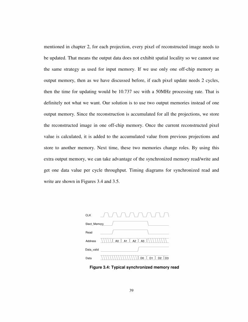
mentioned in chapter 2, for each projection, every pixel of reconstructed image needs to
be updated. That means the output data does not exhibit spatial locality so we cannot use
the same strategy as used for input memory. If we use only one off-chip memory as
output memory, then as we have discussed before, if each pixel update needs 2 cycles,
then the time for updating would be 10.737 sec with a 50MHz processing rate. That is
definitely not what we want. Our solution is to use two output memories instead of one
output memory. Since the reconstruction is accumulated for all the projections, we store
the reconstructed image in one off-chip memory. Once the current reconstructed pixel
value is calculated, it is added to the accumulated value from previous projections and
store to another memory. Next time, these two memories change roles. By using this
extra output memory, we can take advantage of the synchronized memory read/write and
get one data value per cycle throughput. Timing diagrams for synchronized read and
write are shown in Figures 3.4 and 3.5.
Figure 3.4: Typical synchronized memory read
CLK
Slect_Memory
Address
Data_valid
Data
Read
A0
D0
A1 A2 A3
D1 D2 D3

40
Synchronization is critical for this part because when accumulating, the
computing pipeline and the data read from memory must correspond to the same pixel.
3.3 Simple Architecture
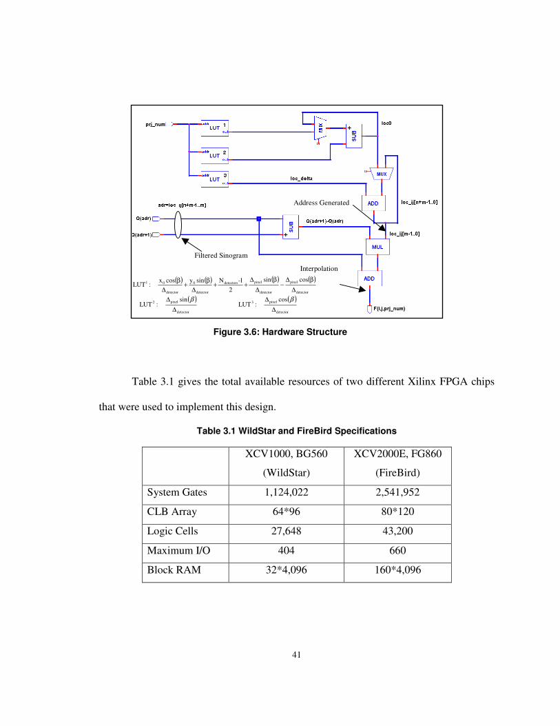
Figure3.6 shows a more detailed hardware structure based on the data flow shown
in Figure 3.3. This design uses three look up tables [3].
The reconstruction begins from the upper-most pixel furthest to the left, and
continues in raster-scan order. For each pixel, once the address of the sinogram is
generated, the corresponding two pieces of sinogram data will be read from memory for
linear interpolation. We define the address generation and interpolation as one
computation.
Figure 3.5: Typical synchronized memory write
CLK
Slect_Memory
Address
Data
Write
A0
D0
A1 A2 A3
D1 D2 D3
41
Table 3.1 gives the total available resources of two different Xilinx FPGA chips
that were used to implement this design.
Table 3.1 WildStar and FireBird Specifications
XCV1000, BG560
(WildStar)
XCV2000E, FG860
(FireBird)
System Gates 1,124,022 2,541,952
CLB Array 64*96 80*120
Logic Cells 27,648 43,200
Maximum I/O 404 660
Block RAM 32*4,096 160*4,096
Filtered Sinogram
Address Generated
Interpolation
Figure 3.6: Hardware Structure
( ) ( ) ( ) ( )detector
pixel
detector
pixeldetectors
detector
0
detector
01 cossin
21-Nsinycosx
:LUT∆
β∆−
∆β∆
++∆
β+∆
β
( )detector
pixel2 sin :LUT
∆∆ β ( )
detector
pixel3 cos :LUT
∆∆ β

42
Our design entry is a combination of user-specified and vendor-provided VHDL
code. Implementation processing is automatically customized for the targeted device by
the design tools. We used Synplicity design tools for VHDL synthesis. To take advantage
of the inherent architectural features of the Xilinx FPGA architectures, such as Fast Carry
Logic for arithmetic functions and on-chip RAM for dual-port and synchronous RAM,
we also used Core Generator, a Xilinx tool. The block RAM component generated by
Core Generator has higher priority than automated block RAM allocation. This means
that if there are still unused block RAMs, the implementation process will use these for
other non-Core Generator Modules when necessary. But if Core Generator Modules
consume all the block RAMs, the implementation process will use other distributed
memory or LUTs to implement other modules instead.
For one projection, the sinogram data is 1024*9=9216 bits. We actually use
16*1024 bits because of the data width requirement of FPGA block RAM (chapter 2), or
4 block RAMs. For pre-loading purpose, we need to store two projections, so we need 8
block RAMs for the sinogram data. In addition, as introduced in chapter 2, we use three
lookup tables to store the initial pixel address and the increment steps. Each lookup table
has 1024 data, with data width 15, 16 and 17 respectively [3]. These lookup tables also
need to be store in memory. If we use block RAMs to store these three lookup tables, 16
block RAMs are needed. For the simple architecture, we still have some block RAMs left
after reserve 8 for sinogram storage. So, we put these three lookup tables in block RAMs,
that is a total of 8+16=24. If we need more block RAMs to store sinogram for a more

43
parallel design (advanced architecture), we can always implement these three lookup
tables in distributed memory. Table 3.2 shows the usage of slices, LUTs and block RAMs
while implementing the simple architecture in both WildStar and FireBird. Although we
use 29 out of 32 block RAMs of WildStar here, most of them (16 block RAMs) are used
for lookup tables. The additional block RAMs are used by the EDA tools for multipliers
or some other components. The usage includes the computation part, memory interfaces
and host interfaces.
Table 3.2 Resource Usage for Simple Architecture
Simple Architecture WildStar FireBird
Usage 1,409 out of 12,288 1,776 out of 19,200 Slice
Percentage 11% 9%
Usage 1,873 out of 24,576 1,582 out of 38,400 4-input
LUT Percentage 7% 4%
Usage 29 out of 32 33 out of 160 Block
RAM Percentage 90% 20%
3.4 Advanced Architecture
To further speed up the processing time, parallel processing is used. Since the
reconstruction processing is independent of one another for different projections, we can
load several projections and process them simultaneously. The number of projections to
be processed depends on the resources available on the FPGA chip. According to Table
3.1, we have sufficient CLBs and block RAMs for a more parallel architecture. Since

44
WildStar and FireBird use different Xilinx FPGA chips, the parallel architectures are
different. We will discuss both cases in the following sections.
3.4.1 WildStar
Due to the size limit of block RAMs on Xilinx Virtex1000, we can maximally
load 4 projections simultaneously. This assumes look-up tables are not stored in block
RAMs. For fast interpolation, we store adjacent sinogram data in different block RAM.
The interface from memory to processor is 64 bits, wide enough to load 4*9 bits for one
read. By using 2 off-chip memories for sinogram data, we can load all four projections in
512 cycles. The data format stored in these two memories is shown in Figure 3.7.
Figure 3.7: Data format in off-chip memory
Projection1Sinogram 1
Projection2Sinogram 1
Projection3Sinogram 1
Projection4Sinogram 1
9 bits 9 bits 9 bits 9 bitsMemory Address
(HEX)
ADDR 0
Projection1Sinogram 3
Projection2Sinogram 3
Projection3Sinogram 3
Projection4Sinogram 3ADDR 1
Projection1Sinogram 1023
Projection2Sinogram 1023
Projection3Sinogram 1023
Projection4Sinogram 1023ADDR 1FF
Projection5Sinogram 1
Projection6Sinogram 1
Projection7Sinogram 1
Projection8Sinogram 1ADDR 200
Projection5Sinogram 3
Projection6Sinogram 3
Projection7Sinogram 3
Projection8Sinogram 3ADDR 201
Projection1021Sinogram 1023
Projection1022Sinogram 1023
Projection1023Sinogram 1023
Projection1024Sinogram 1023ADDR 1FFFF
36 Bits
Four projections
Projection1Sinogram 2
Projection2Sinogram 2
Projection3Sinogram 2
Projection4Sinogram 2
9 bits 9 bits 9 bits 9 bits
Projection1Sinogram 4
Projection2Sinogram 4
Projection3Sinogram 4
Projection4Sinogram 4
Projection1Sinogram 1024
Projection2Sinogram 1024
Projection3Sinogram 1024
Projection4Sinogram 1024
Projection5Sinogram 2
Projection6Sinogram 2
Projection7Sinogram 2
Projection8Sinogram 2
Projection5Sinogram 4
Projection6Sinogram 4
Projection7Sinogram 4
Projection8Sinogram 4
Projection1021Sinogram 1024
Projection1022Sinogram 1024
Projection1023Sinogram 1024
Projection1024Sinogram 1024
36 Bits
Odd Sinograms Even Sinograms

45
3.4.2 FireBird
From Table 3.1, we see that the FPGA chip, XCV2000E used in FireBird has
more CLBs and more block RAMs. The bottleneck in the WildStar parallel design is the
block RAMs. So if we have more block RAM, we can process more projections at the
same time to shorten the processing time. This also means that we need to load more
projections from off-chip memory banks.
From Figure 3.7, we see that we have not fully utilized the two off-chip memories’ I/O
bandwidth; the memory width is 64 bits while we only use 36 bits of it. A direct solution
would be to load 7*9 bits simultaneously, that is 7 projections at the same time.
EvenRAM
512*9 bits
OddRAM
512*9 bits
EvenRAM
512*9 bits
OddRAM
512*9 bits
EvenRAM
512*9 bits
OddRAM
512*9 bits
EvenRAM
512*9 bits
OddRAM
512*9 bits
MemoryBank Even64-bit width
9 Bits
9 Bits
9 Bits
9 Bits
9 Bits
MemoryBank Odd
64-bit width
9 Bits
9 Bits
9 Bits
EvenRAM
512*9 bits
OddRAM
512*9 bits
EvenRAM
512*9 bits
OddRAM
512*9 bits
EvenRAM
512*9 bits
OddRAM
512*9 bits
EvenRAM
512*9 bits
OddRAM
512*9 bits
36Bits
36Bits
Processing
Figure 3.8: Parallel loading of 4 projections using two input memories

46
Furthermore, if we use four memory banks for input memory instead of two, we can
double the parallel processing to 2*7=14. This is a method for increasing the off-chip
memory I/O bandwidth. This method is limited by the memory access time and the
number of memories available, which is fixed for a specific computing board. For
FireBird, we have four 64 bit-width and one 32 bit-width memories. For two 64-bit width
memories, the maximum number of projections that can be loaded in parallel is 14.
Therefor, the maximum number of projections that can be processed simultaneously in
FireBird is 14. Figure 3.8 and 3.9 shows the logic block organization for parallel loading
4 projections for WildStar and 14 projections for FireBird, respectively.
EvenRAM
512*9 bits
OddRAM
512*9 bits
EvenRAM
512*9 bits
OddRAM
512*9 bits
EvenRAM
512*9 bits
OddRAM
512*9 bits
EvenRAM
512*9 bits
OddRAM
512*9 bits
MemoryBank Even64-bit width
9 Bits
9 Bits
9 Bits
9 Bits
MemoryBank Odd
64-bit width
9 Bits
EvenRAM
512*9 bits
OddRAM
512*9 bits
EvenRAM
512*9 bits
OddRAM
512*9 bits
7*9=63BitsMaximum data width provided
by memory banksEvenRAM
512*9 bits
OddRAM
512*9 bits
EvenRAM
512*9 bits
OddRAM
512*9 bits
...
EvenRAM
512*9 bits
OddRAM
512*9 bits
EvenRAM
512*9 bits
OddRAM
512*9 bits
EvenRAM
512*9 bits
OddRAM
512*9 bits
EvenRAM
512*9 bits
OddRAM
512*9 bits
MemoryBank Even64-bit width
9 Bits
9 Bits
9 Bits
9 Bits
MemoryBank Odd
64-bit width
9 Bits
EvenRAM
512*9 bits
OddRAM
512*9 bits
EvenRAM
512*9 bits
OddRAM
512*9 bits
7*9=63BitsMaximum data width provided
by memory banksEvenRAM
512*9 bits
OddRAM
512*9 bits
EvenRAM
512*9 bits
OddRAM
512*9 bits
...
9 Bits
9 Bits
9 Bits
9 Bits
9 Bits
9 Bits
Processing
Figure 3.9: Parallel loading 14 projections using four input memories

47
However, if we use four memory banks as input memories, we have only one 32-
bit memory bank for output. Then the memory structure we discussed previously for
output cannot be implemented. Using one output memory means we have to waste
several clock cycles for each read and write. These wasted clock cycles are much longer
than the loading time we saved.
Instead of using the method discussed above, we extended the loading time so that
we can save two off-chip memory banks for output. Figure 3.10 shows that we only
introduce a small portion of delay by extending the loading time.
The “4-way” and “8-way” labels in the figure mean that 4/8 projections are
loaded and processed simultaneously.
Projection 1-4
ProjectionLoading
ProjectionProcessing
Projection 1-4
Projection 5-8 Waiting
Time
Projection 1-8
ProjectionLoading
ProjectionProcessing
Projection 1-8
Projection 9-16 Waiting
Projection 9-16
Projection 17-24 Waiting
Projection 17-24
Projection 25-32 Waiting
Projection 5-8
Projection 9-12 Waiting
Projection 9-12
Projection 13-16 Waiting
�t
4-way
8-way
Figure 3.10: Extending the loading time

48
Since the processing time is 512*512 cycles, much longer than the loading time,
the loading of projections overlaps with the processing. We only extend the first loading
time; the following projection loading can be done in parallel.
Table 3.3 gives the resource usage of the advanced architecture for both WildStar
and FireBird. For both implementations, the block RAMs are the bottleneck to further
speedup. If we use a more advanced FPGA chip, such as Virtex II, this structure is
expandable to more parallel implementation.
Table 3.3 Resource Usage for Advanced Architecture
Advanced Architecture WildStar
(4-way)
FireBird
(16-way)
Usage 4,853 out of 12,288 5,679 out of 19,200 Slice
Percentage 39% 29%
Usage 7,668 out of 24,576 8,162 out of 38,400 4-input
LUT Percentage 31% 21%
Usage 32 out of 32 144 out of 160 Block
RAM Percentage 100% 90%
3.5 Adaptive Module
Another issue we met in our implementation is that when we change the board,
we also have to change the VHDL code. Due to the different chip, different board
structure and different user supplied interface, if we fail to design the memory

49
architecture and interface carefully, we have to change a large part of the code when
changing the board. To avoid this, we insert an adaptive module between the memory
interface and the core design to de-couple these two parts. By doing this, we can
maximize the reuse of the VHDL code. Figure 3.11 shows the logical connection
between these three modules.
As we have mentioned before, WildStar and FireBird are quite different
computing boards. They use different FPGA chips and have different board layout.
Moreover, the user-supplied interfaces are different for these two boards. In the following
paragraphs, we will discuss these differences.
First, for different target FPGA chips, most synthesis tools provide a large library
of different FPGA chips. By simply changing the parameters, the tools will automatically
Memory Interface
Core Design
Adaptive Module
Pro
cess
ing
Ele
men
t
On-board Memory
Add
ress
Dat
a
Con
trol
Figure 3.11: Interface adaptive module

50
generate the bit file specific to the FPGA you are using. The HDL code does not need to
be modified in this case.
Second, different board layout, is more complicate than the first case. The size of
the memory banks and the connections between off-chip memory banks and FPGA chips
inevitably influences the design. It is the designer’s responsibility to make sure the off-
chip memory banks are large enough to store the data. As for the different physical
connections between memory banks and FPGA chips, we can build a universal logic
structure by carefully select names of the signals. For example, in WildStar, the memory
banks used to store sinograms are called PE1_LEFT_MEZZ_MEM0_BANK and
PE1_RIGHT_MEZZ_MEM0_BANK; we rename them to InputMemLeft and
InputMemRight. In FireBird, the memory banks we use to store sinograms are
MEM_0_BANK and MEM_1_BANK; we also call them InputMemLeft and
InputMemRight. The universal names for the input memories hide the details of the
physical location of the off-chip memory banks. For the core design, we just use these
names as the interface signals and do not need to worry about the details.
The third case is different interface code supplied to the user from the board
manufacture. The user-supplied interface is VHDL code that uses standard logic signals
to communicate between FPGA and off-chip memories. We can ignore the details of the
physical characteristics of the memory and actual board layout by using these interfaces;
all we are concerned about are the handshaking signals they provided. But unfortunately,
the handshaking signals are different for different boards. For a memory-intensive

51
application, a lot of control signals depend on these signals. Moreover, synchronization
between memory read/write and computation are extremely important in our application.
When we start or stop the calculation relies on when we get valid data. If the handshaking
signals are different, using the adaptive module is essential for maximum reuse of the
VHDL code.
The main task of the adaptive module is to utilize the handshaking signals
provided by the user-supplied interface and translate them to some essential and standard
signals. The core design makes use of these standard signals so that even if the interface
changes, the core will still operate as usual.
Let’s take our implementation as an example. A simplified list of handshaking
signals from the WildStar and FireBird user-supplied interfaces is described in Table 3.4.
Table 3.4 WildStar and FireBird handshaking signals
WildStar FireBird To interface
Clock Strobe Write Address
Clock Request Write Address
Read
From Interface
Data Data_valid
Data Data_valid Acknowledge
To interface
Clock Strobe Write Address Data
Clock Request Write Address Data
Write
From Interface
Acknowledge

52
The functionality for each signal is as follows:
Clock: Access rate to the memory. It depends on the memory access time. In our
implementation, it is synchronized to the processing clock in the core design.
Strobe or Request: This signal is used to signify which memory is used. Any read/write
signals are invalid on a given memory until this signal is high.
Write: Indicates current operation is a read or write procedure. If Write = ‘1’, then write
to memory; if Write = ‘0’, then read from memory.
Address: The memory address where data is stored.
Data: What needs to be read out or written to the memory.
Data_valid: Signals to the user that the data requested is valid on the data bus.
Acknowledge: The read/write request is accepted and the interface is ready for a new
read/write operation.
Clearly, WildStar and FireBird use different handshaking signals. Moreover, in
our actual implementation, there are some other differences such as the data bus width,
the maximum memory storage etc. The memories must be arranged for each
implementation so that there are enough memories and enough memory size to store both
the input data and the output data.
As we have discussed already, to avoid wasting several cycles each time we
read/write, we use a pipelined structure and synchronized burst read/write in our
application. For those interfaces with acknowledge signals, we can easily tell if the

53
memory access time is less than a clock cycle. From Table 3.4, we know WildStar does
not have an acknowledge signal. Then it is our responsibility to detect and prevent data
conflict. That is, in case the data is not steady on the data bus when reading or the hold
time is not long enough when writing data, we should detect this and use some
mechanism to either prevent or correct the problem. An easy way to do so is to reduce the
clock frequency so that we can make sure data is read/written in one clock cycle.
The purpose of the adaptive module is to hide the differences between different
target technologies and provide the same handshaking signals to the core design
independent of the specific board. Another attractive feature of the adaptive module is
that it won’t degrade the hardware performance when using a pipelined structure.
Some pseudo-code is provided below in VHDL format to present a brief idea of
what the adaptive module looks like. The actual processes are much more complicated
than this. Here, the Address Update Process (AUP) and Memory Control Signal Update
Process (MCSUP) belong to the adaptive module. The Data Computing Process (DCP) is
part of the core design.
******************************************************************* AUP: Process (clk, reset) Begin if(reset = '1') then address <= some initial value; elsif(rising_edge(clk)) then ------------------------------------------- -- If memory interface provides ack signal -- if(ack = '1') then -- address <= next address; -- end if; -- end if; ------------------------------------------- address <= next address; -- No ack signal end if; End process *******************************************************************

54
******************************************************************* MCSUP: Process(clk,reset) Begin if(reset = '1') then set to initial state;
no read/write request; elsif(rising_edge(clk)) then check if core design is ready to read/write; ------------------------------------------- -- If memory interface provides ack signal -- if(ack = '1') then -- send next read/write request; -- end if; -- end if; ------------------------------------------- send next read/write request; -- No ack signal end if; End process ******************************************************************* ******************************************************************* DCP: Process(clk, data_valid) Begin if(rising_edge(clk)) then if(data_valid = '1') then process the data; else stall the pipeline and wait for the data_valid signal; end if; End process; *******************************************************************
The function of these three process is described below:
AUP: This process is quite simple. It just updates the addresses each clock cycle
if no acknowledge signal is available. That is why we emphasized previously that we
should make sure the memory access time should be less than one clock cycle. If this
condition is not satisfied, we may not get the correct data. Of course, if the vendor
provides an acknowledge signal, we can use this signal to detect conflict.
MCSUP: This process decides the moment to start read/write operation. When the
memory access is simple, this process can be combined with AUP; the memory control
signal and address update can be handled in the same process. Again, the acknowledge
signal is very useful here since it gives an indication of successful operation.

55
DCP: Data Computing Process is part of the core design. Clearly, when we have
the adaptive module, the memory access is very simple. The DCP only sends out the
request and, once the data is ready, processes this data and sends a request for the next
address. The next address can either be determined by the AUP if it is consecutive or by
the core design if the address needs to be generated through computation.
3.6 Summary
In this chapter, we presented the FPGA implementation in detail. We
concentrated on bit width selection and memory architecture organization for this specific
application; the same ideas can also be used for other data-intensive applications. Usage
of hardware resources is introduced for both a simple architecture and an advanced
architecture for two different target FPGA computing boards.
The motivation for introducing the adaptive module and its function are also
included in this chapter. By adding this module, we can greatly improve the HDL code
re-use.

56
Chapter 4
Results and Performance
Several medical images are used to verify our hardware implementation results.
The processing time for WildStar and FireBird, simple architecture and advanced
architecture, are also listed to show the speedup. Moreover, our results show that
inserting the adaptive module won’t affect the performance, while it can greatly increase
the re-use of the original VHDL code when changing the target technology.
4.1 Results
Hardware reconstructed images are compared with floating-point software
reconstructed images. As proved in [3], the relative error is small enough, thus the visual
effects of hardware reconstructed images are good enough for medical purposes. Figure
4.1 shows the heart images with different reconstruction processes. Figure 4.2 enlarges a
part of figure 4.1. The mapping between the grayscale range and the pixel value range
was manually adjusted to show the image in more detail. This illustrates the high quality
medical images reconstructed by our approach.

57
Software reconstruction
(Floating Point)Hardware reconstruction
(Fixed Point)
Relative Error
Sinogram quantization : 9 bits
Interpolation factor: 3 bits
Relative Error: 0.001295%
Figure 4.1: Reconstructed image comparison
Figure 4.2: Reconstructed image comparison, enlarged
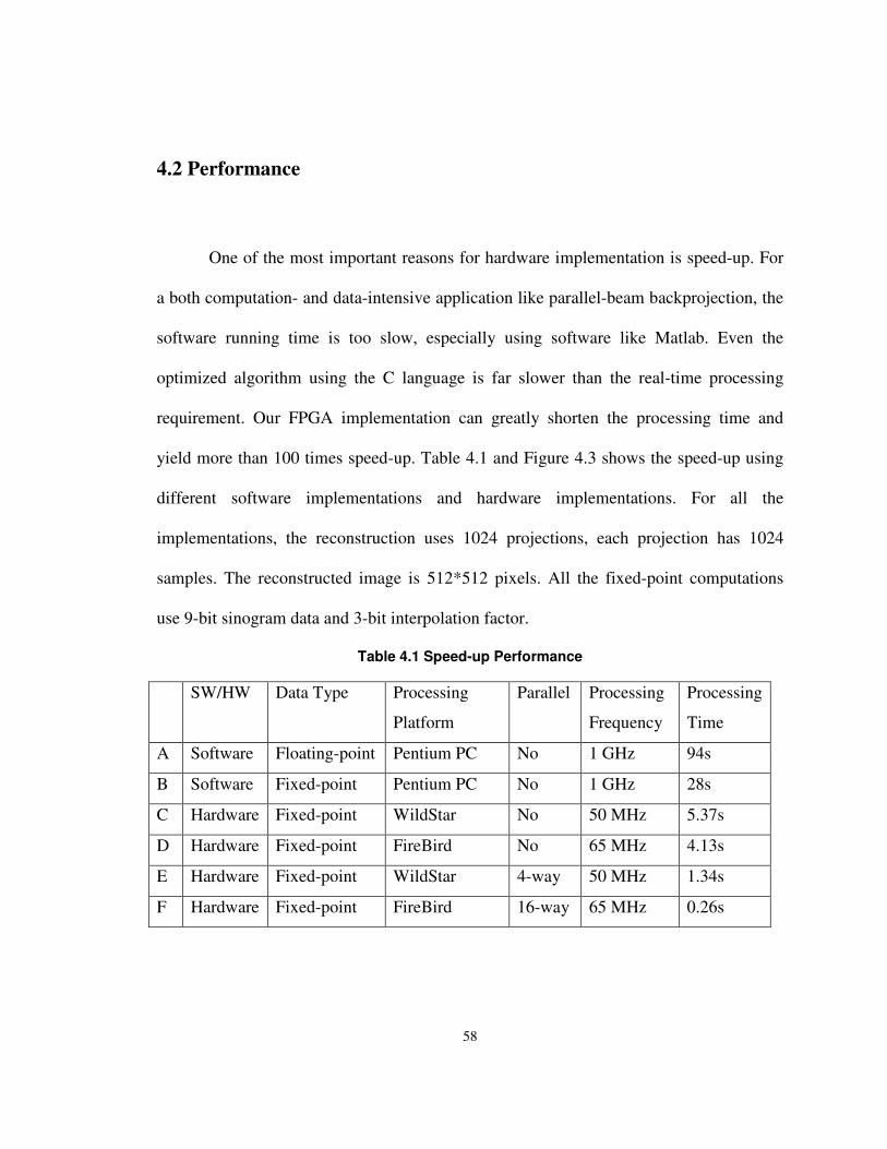
58
4.2 Performance
One of the most important reasons for hardware implementation is speed-up. For
a both computation- and data-intensive application like parallel-beam backprojection, the
software running time is too slow, especially using software like Matlab. Even the
optimized algorithm using the C language is far slower than the real-time processing
requirement. Our FPGA implementation can greatly shorten the processing time and
yield more than 100 times speed-up. Table 4.1 and Figure 4.3 shows the speed-up using
different software implementations and hardware implementations. For all the
implementations, the reconstruction uses 1024 projections, each projection has 1024
samples. The reconstructed image is 512*512 pixels. All the fixed-point computations
use 9-bit sinogram data and 3-bit interpolation factor.
Table 4.1 Speed-up Performance
SW/HW Data Type Processing
Platform
Parallel Processing
Frequency
Processing
Time
A Software Floating-point Pentium PC No 1 GHz 94s
B Software Fixed-point Pentium PC No 1 GHz 28s
C Hardware Fixed-point WildStar No 50 MHz 5.37s
D Hardware Fixed-point FireBird No 65 MHz 4.13s
E Hardware Fixed-point WildStar 4-way 50 MHz 1.34s
F Hardware Fixed-point FireBird 16-way 65 MHz 0.26s

59
As expected, the FPGA implementations give considerable speed-up compared to
software using the same algorithm. For software computation, although the PC works at
1GHz, it has to follow the Von-Neumann concept; that is, instruction fetch, instruction
decode, instruction execution. The general-purpose structure introduces a lot of overhead
for specific computation, thus the computing time is long. Our FPGA implementation is
designed for this application and the memory architecture as well as the hardware
component are optimized for fast processing. Even though the system works at a much
lower frequency, 50~65MHz, it is much more efficient than the software implementation.
Figures 4.4 and 4.5 show the layout of the FPGA chip generated by the Xilinx tools.
The layout of the design can influence the maximum processing frequency since routing
0
10
20
30
40
50
60
70
80
90
100
A B C D E F
Pro
cess
ing
Tim
e (s
econ
d)
Figure 4.3: Processing time comparison

60
delay cannot be ignored in FPGA design. We let the EDA tools decide where to place the
components and how to route them. This procedure can also be done by hand which may
yield a better solution but a much longer design circle.
Figure 4.4: Chip layout for simple architecture in Virtex 2000E
Figure 4.5: Chip layout for advanced architecture in Virtex 2000E

61
The colored parts of the chip layout are the hardware resources used for the
application while the gray part means unused. The vertical lines are where the on-chip
block RAMs are located. Comparing these two figures, the 16-way advanced architecture
uses many more resources than the simple architecture. Moreover, although most of the
block RAMs are used in the advanced architecture, we still have plenty of unused CLBs.
That means the block RAMs are the bottleneck to a more parallel structure. For an FPGA
chip with more block RAMs, we can process more projections at the same time and
further achieve more speed-up.
An important result of this research is the use of the adaptive module. The
adaptive module allows us to reuse the VHDL code for the core design with no changes.
Although it is difficult to give a numerical result for code re-use, we can estimate the
percentage of affected lines to illustrate its usefulness. For our FireBird advanced
architecture (see Appendix A), the code is composed of three parts: core design, adaptive
module and other declaration code. The Core design uses 1629 lines out of 2180 lines,
that is 74.72% of the user-specified code, while the adaptive module uses only 247 lines,
11.33% of the code. For the case where we are migrating from one board to another, we
can keep at least the 74.72% of the code untouched. Some modifications are required for
the adaptive module and very few modifications are needed for the other declaration
code. Moreover, the processing time is not affected by this module in our implementation
since the processing delay is 108 clock cycles while adding the adaptive module only

62
increases the delay by less than 10 clock cycles. The throughput of the system is the same
whether we use adaptive module or not.
4.3 Summary
In this chapter, we compared the hardware reconstruction results with software
results and confirm that the visual effect is not compromised. This is the prerequisite of
our hardware implementation. The processing time using software and different hardware
are also listed. For the same algorithm, using Xilinx Viretex 2000E FPGA can achieve
more than 100 times speed-up and shorten the reconstruction time of one image to 0.26s.
Actual chip layouts are also shown in this chapter and gives the conclusion that more
parallelism depends on the availability of on-chip block RAMs.
63
Chapter 5
Conclusion and Future Work
5.1 Conclusion
Most image-processing applications are both computationally and data intensive.
Software processing takes a long time and is not suitable for real-time processing.
Hardware becomes a candidate for fast processing since it can provide an optimized
design specific to the application. FPGA implementation is chosen for our parallel-beam
backprojection application because of its flexibility and short design circle. For such a
large amount of processing data to be processed, we need extra external memory banks to
store them and interfaces to communicate between the FPGA chip and these memory
banks. Frequent read/write from/to off-chip memory results in long delays due to the
access delay of the off-chip memories. Two-stage memory access, basically the same
idea as using cache memory in computer architecture, utilizes the locality of reference
property [19] of memory accesses and is proved to be a successful approach for the
backprojection application. Moreover, it can be generalized to apply to other data
intensive applications as long as they satisfy the locality of reference property. That is,
references to memory at any given time interval tend to be confined to within a few
64
localized areas in memory. Our results show the hardware implementation can achieve
more than 100 times speed-up compared to the software.
Another issue we met in our design is the memory interface. If we change the
target technology, we need to change HDL code accordingly. When the memory interface
changes, we may need to rewrite a large part of the code, which is very time-consuming.
To maximally re-use the original code, we put an adaptive module between the memory
interface and the core design to de-couple them. Again, our different hardware
implementations prove this extra module can greatly reduce the effort while migrating a
design to a different platform. The extra delay is insignificant compared to the total delay
of the design in our case. This concept can also extended to any designs with memory
interfaces.
5.2 Future Work
Currently, our bottleneck for further parallelism in the backprojection
implementation is the block RAM. The hardware structure is expandable to a more
advanced architecture as long as there are enough hardware resources. Therefore, with a
higher density FPGA chip with more block RAMs, we can further increase the speed-up.
The hardware structure we use in this thesis comes from previous work [3]. To save the
sinogram loading time, foreground and background block RAMs are used. While the data

65
in foreground block RAMs are processed, the background block RAMs load the
sinogram data for the next processing cycle. Next time, foreground and background block
RAMs exchange their role. However, as we have discussed in previous chapters, block
RAMs are the bottleneck of further parallelism. Although the block RAMs organization
can save loading time, it doubles the requirement for the on-chip memory resource.
Therefore, if we don’t reserve half of the block RAMs for background data, we can
double the parallel processed projections. For example, in WildStar, we can process 8
projections simultaneously instead of 4. Since the loading time is much less than the
processing time, we can further reduce the processing time by this means.
Assume the processing time using the current hardware structure is TP, the
loading time is TL, while TL<< TP. The total reconstruction time is TP due to the overlap
of loading and processing. However, if we change the hardware structure to what we
propose here, the processing time would be TP/2, and the loading time is still TL. The
final reconstruction time would be TP/2+ TL. Which is less than our current hardware
structure. Moreover, the new proposed hardware structure is expandable to an even more
parallel structure if there are enough hardware resources.
Another hot application for medical imaging is cone-beam backprojection. It
reconstructs the 3D image of a scanned object, the computation complexity is O(N4).
Clearly, the amount of input and output data are much larger than for 2D reconstruction.
For hardware implementation, the requirements of memory architecture and computation
are much higher than for our current parallel-beam backprojection. It would be another

66
challenge to design the hardware structure and select the right FPGA architecture for
reconfigurable hardware implementation.
67
Bibliography
[1] Vaughn Betz, Jonathan Rose and Alexander Marquardt, “Architecture and CAD for
Deep-Submicro FPGAs”, Kluwer Academic Publishers, USA, 1999.
[2] Kak, A.C., and Slaney, M., “Principles of Computerized Tomographic Imaging”,
New York, IEEE Press, 1988.
[3] Srdjan Coric, “Parallel-Beam Backprojection: an FPGA Implementation Optimized
for Medical Imaging”, M.S. Thesis, Dept of Electrical and Computer Engineering,
Northeastern University, May, 2002.
[4] Srdjan Coric, Miriam Leeser and Eric Miller, “Parallel-Beam Backprojection: An
FPGA Implementation Optimized for Medical Imaging”, Tenth ACM Int. Symposium on
Field-Programmable Gate Arrays, Monterey, CA, USA, Feb. 24-26, 2002.
[5] “VirtexTM 2.5V Field Programmable Gate Arrays”, Xilinx website,
http://direct.xilinx.com/bvdocs/publications/ds003.pdf, last accessed on May 29, 2003.
[6] “VirtexTM-E 1.8V Field Programmable Gate Arrays”, Xilinx website,
http://direct.xilinx.com/bvdocs/publications/ds022.pdf, last accessed on May 29, 2003.
[7] “WildStarTM Reference Manual”, revision 3.0, Annapolis Micro Systems Inc., 2000.
[8] “FireBirdTM Reference Manual”, revision 3.0, Annapolis Micro Systems Inc., 2000.
[9] Wu. M.A., “ASIC Applications in Computed Tomography Systems,” Proceedings of
Fourth Annual IEEE International ASIC Conference and Exhibit, Rochester, NY, USA
1991, pp.P1-3/1-4.
[10] Agi, I., Hurst, P.J., and Current, K.W., “An image processing IC for backprojection
and spatial histogramming in a pipelined array,” IEEE Journal of Solid-state Circuits,
vol. 28, no. 3, 1993, pp. 210-221.

68
[11] Agi, I., Hurst, P.J., and Current, K.W., “A VLSI architecture for high-speed image
reconstruction: considerations for a fixed-point architecture,” Proceedings of SPIE,
Parallel Architectures for Image Processing, vol. 1246, 1990, pp. 11-24.
[12] Stephen G. Azevedo, Brian K. Cabral and J. Foran, “Tomographic image
reconstruction and rendering with texture-mapping hardware,” Proceedings of
Mathematical Methods in Medical Imaging III, SPIE, vol. 2299, 1994, pp. 280-289.
[13] Luiz Maltar C.B., Felipe M.G. Franca, Vladimir C. Alves, Claudio L, Amorim,
“Reconfigurable Hardware for Tomographic Processing,” Proceedings of the XI
Brazilian Symposium on Integrated Circuit Design, IEEE Computer Society Press, Rio
de Janeiro/RJ, 1998, pp. 19-24.
[14] Basu, S., and Bresler, Y., “O(N2log2N) filtered backprojection reconstruction
algorithm for tomography,” IEEE Transactions on Image Processing, vol. 9, no. 10, Oct
2000, pp. 1760-1773.
[15] Chen, Chung-Ming, Cho, Zang-Hee, and Wang, Cheng-Yi, “A Fast Implementation
of the Incremental Backprojection Algorithms for Parallel Beam Geometries,” IEEE
Transactions on Nuclear Science, vol. 43, no. 6, Dec 1996, pp. 3328-3334.
[16] Bins, J., Draper, B., Bohm, W., and Najjar, W., “Precision vs. Error in JPEG
Compression,” Parrallel and Distributed Methods for Image Processing III (SPIE),
Denver CO, Jul 22, 1999, pp. 76-87.
[17] Joonseok Park and Pedro Diniz, “Synthesis and Estimation of Memory Interfaces for
FPGA-based Reconfigurable Computing Engines”, Proc. of the 2003 IEEE Symposium
on FPGAs for Custom Computing Machines (FCCM'03), IEEE Computer Society Press,
Los Alamitos, California, April 2003.

69
[18] G.W. Donohoe, K.J. Hass, S. Bruder, and P.-S. Yeh, “Reconfigurable Data Path
Processor for Space Applications”, Proc. Military and Aerospace Applications of
Programmable Logic Devices 2000, Laurel, MD, September 24-28, 2000.
[19] M. Morris Mano, “Computer System Architecture, Third Edition”, Prentice-Hall,
New Jersey, 1993.

70
Appendix A
16-way Parallel Implementation – VHDL code
--======================================================-- -- -- -- NORTHEASTERN UNIVERSITY -- -- DEPARTMENT OF ELECTRICAL AND COMPUTER ENGINEERING -- -- RAPID PROTOTYPING LABORATORY -- ---------------------------------------------------------- -- FILE | bckp_16prj_arch_debug.vhd -- -- -------------+------------------------------------ -- -- DESCRIPTION | 16 projection parallel processing -- -- | of backprojection -- -- | debug version -- -- -------------+------------------------------------ -- -- AUTHOR | Haiqian Yu -- -- -------------+------------------------------------ -- -- DATE | Sep. 12, 2002 -- --======================================================-- --******************************************************************************-- -- -- -- Copyright (C) 2000 Haiqian Yu -- -- -- -- This program is free software; you can redistribute it and/or -- -- modify it under the terms of the GNU General Public License -- -- as published by the Free Software Foundation; either version 2 -- -- of the License, or (at your option) any later version. -- -- -- -- This program is distributed in the hope that it will be useful, -- -- but WITHOUT ANY WARRANTY; without even the implied warranty of -- -- MERCHANTABILITY or FITNESS FOR A PARTICULAR PURPOSE. See the -- -- GNU General Public License for more details. -- -- -- -- You should have received a copy of the GNU General Public License -- -- along with this program; if not, write to the Free Software -- -- Foundation, Inc., 59 Temple Place - Suite 330, Boston, MA 02111-1307, USA. -- -- -- --******************************************************************************-- -------------------------- Library Declarations ------------------------ -- IEEE Libraries -- library IEEE; use IEEE.std_logic_1164.all; use IEEE.std_logic_arith.all; use IEEE.std_logic_unsigned.all; library LAD_Mux_Lib;

71
use LAD_Mux_Lib.LAD64_Mux_pkg.all; use LAD_Mux_Lib.LAD64_Mem32_Mux_pkg.all; use LAD_Mux_Lib.LAD64_Mem64_Mux_pkg.all; library Mem_Mux_Lib; use Mem_Mux_Lib.Mem32_Mux_pkg.all; use Mem_Mux_Lib.Mem64_Mux_pkg.all; library PE0_Lib; use PE0_Lib.all; use PE0_Lib.utilities.all; -------------------------- Entity ------------------------ ENTITY Advanced_Arch IS GENERIC ( Mask : std_logic_vector(15 DOWNTO 0) := x"0000"; Base : std_logic_vector(15 DOWNTO 0) := x"0000" ); PORT ( Kclk : IN std_logic; Mclk : IN std_logic; Pclk : IN std_logic; Reset : IN std_logic; LAD : INOUT LAD64_Mux; InputMemLeft : INOUT Mem64_Mux; InputMemRight : INOUT Mem64_Mux; OutputMemEven : INOUT Mem64_Mux; OutputMemOdd : INOUT Mem64_Mux ); END Advanced_Arch; -------------------------- Architecture ------------------------ ARCHITECTURE behavioral OF Advanced_Arch IS -- Types -- type ControlStateMach is ( StatePowerup1, StatePowerup2_IMLeft, StatePowerup3_IMLeft, StatePowerup2_IMRight, StatePowerup3_IMRight, StatePowerup2_OMEven, StatePowerup3_OMEven, StatePowerup2_OMOdd, StatePowerup3_OMOdd, StateInit, StateReset, StateStart, StateWait, StatePipe1, StatePipe2, StatePipe3, StatePipe4, StatePipe_last, StateEnd ); type ControlPipeMach is ( PipeInit, PipeStage1_fill, PipeStage2_fill, PipeStage3_fill, PipeStage4_fill, PipeStage5_fill, PipeStage6_fill, PipeStage7_fill, PipeStage8_fill, PipeStage1_empty, PipeStage2_empty, PipeStage3_empty, PipeStage4_empty, PipeStage5_empty, PipeStage6_empty, PipeStage7_empty, PipeStage8_empty, PipeStage9_empty );

72
-- user defined components. COMPONENT Round_unsigned IS GENERIC ( total_data_width:NATURAL ); PORT ( data_in:IN std_logic_vector(total_data_width-1 DOWNTO 0); data_out:OUT std_logic_vector(total_data_width-1-1 DOWNTO 0) ); END COMPONENT; COMPONENT address_demux IS GENERIC ( address_width:NATURAL ); PORT ( address_in:IN std_logic_vector(address_width-1 DOWNTO 0); address_out_even:OUT std_logic_vector(address_width-1-1 DOWNTO 0); address_out_odd:OUT std_logic_vector(address_width-1-1 DOWNTO 0) ); END COMPONENT; -- vectors. TYPE array_bit_15 IS ARRAY (1 TO 16) OF std_logic_vector(14 DOWNTO 0); TYPE array_bit_16 IS ARRAY (1 TO 16) OF std_logic_vector(15 DOWNTO 0); TYPE array_bit_17 IS ARRAY (1 TO 16) OF std_logic_vector(16 DOWNTO 0); TYPE array_bit_25 IS ARRAY (1 TO 16) OF std_logic_vector(24 DOWNTO 0); TYPE array_bit_26 IS ARRAY (1 TO 16) OF std_logic_vector(25 DOWNTO 0); TYPE array_bit_4 IS ARRAY (1 TO 16) OF std_logic_vector(3 DOWNTO 0); TYPE array_bit_9 IS ARRAY (1 TO 16) OF std_logic_vector(8 DOWNTO 0); TYPE array_bit_1 IS ARRAY (1 TO 16) OF std_logic; TYPE array_bit_9_4 IS ARRAY (1 TO 4) OF std_logic_vector(8 DOWNTO 0); TYPE array_bit_10 IS ARRAY (1 TO 16) OF std_logic_vector(9 DOWNTO 0); TYPE array_bit_14 IS ARRAY (1 TO 16) OF std_logic_vector(13 DOWNTO 0); TYPE array_bit_13 IS ARRAY (1 TO 18) OF std_logic_vector(12 DOWNTO 0); TYPE array_bit_16_8 IS ARRAY (1 TO 8) OF std_logic_vector(15 DOWNTO 0); TYPE array_bit_17_4 IS ARRAY (1 TO 4) OF std_logic_vector(16 DOWNTO 0); TYPE array_bit_18_2 IS ARRAY (1 TO 2) OF std_logic_vector(17 DOWNTO 0); -- Constants -- constant BlockRam_AddrWidth : natural:=9; constant BlockRam_DataWidth : natural:=9; -- Signals -- signal ControlPresentState : ControlStateMach; signal ControlNextState : ControlStateMach; -- Signals in ControlStateMachine signal readReset_IM : std_logic; signal readEn_IM : std_logic; signal writeReset_OM : std_logic; signal readReset_OM : std_logic; signal PowerUpEven_Read : std_logic; signal PowerUpOdd_Read : std_logic; signal done : std_logic; signal Power_Pipe : std_logic; signal en_ld_BR1 : std_logic; signal en_rd_BR1: std_logic; signal en_ld_BR2: std_logic; signal en_rd_BR2: std_logic; signal pixcnt_reset: std_logic; signal prj_SCLR: std_logic; signal pipe_reg_reset: std_logic; signal even_turn: std_logic; signal stall: std_logic; -- Signals used for state change. signal Registers: LAD64_Mux_register_vector(0 to 1); signal start: std_logic := '0'; signal last_br_address_even: std_logic; signal last_br_address_odd: std_logic; signal last_br_address: std_logic; signal wait_data_valid_zero: std_logic; signal prjs_loaded: std_logic; signal current_prj_read_done: std_logic; signal delayed: std_logic;

73
-- Pixel counters control signal and outputs signal pixel_counter_reset: std_logic; signal last_pixel: std_logic; signal new_row: std_logic; signal pipe_reg1_new_row: std_logic; signal u_en_pixel_counter: std_logic; signal pixel_zero: std_logic; signal pipe_reg1_pixel_zero: std_logic; signal current_pixel_addr: std_logic_vector(17 downto 0); -- Projection Counter control signal and outputs. signal prj_num: std_logic_vector(5 downto 0); signal current_prj_done: std_logic; signal u_prj_counter_ce: std_logic; signal last_prj_reached: std_logic; -- Look up tables value signal lut1_dout: array_bit_15; signal lut2_dout: array_bit_16; signal lut3_dout: array_bit_17; -- Input memory interface signals. signal readAddr_IML: std_logic_vector(31 downto 0); signal readDone_IML: std_logic; signal readAddr_IMR: std_logic_vector(31 downto 0); signal readDone_IMR: std_logic; -- Output memory interface signals. signal OutputMem_reg1_din: std_logic_vector(25 downto 0); signal OutputMem_reg1_dout: std_logic_vector(25 downto 0); signal OutputMem_reg2_dout: std_logic_vector(25 downto 0); -- Projection to process, get from register. signal prj_to_process: std_logic_vector(9 downto 0); -- Mux selection signals. signal u_pipe_stage2_mux_S: std_logic; signal u_pipe_stage3_mux_S: std_logic; -- Component enable signals signal u_pipe_stage2_subtracter_ce: std_logic; signal u_pipe_stage3_adder_ce: std_logic; signal u_pipe_reg4_ifactor_ce: std_logic; signal u_pipe_reg5_ifactor_ce: std_logic; signal u_interpolation_sub_ce: std_logic; signal u_pipe_reg5_switch_out_b_ce: std_logic; signal u_multiplier_ce: std_logic; signal u_pipe_reg6_switch_out_b_ce: std_logic; signal u_prj_acc_adder_ce: std_logic; signal u_blkram1_rd_ce: std_logic; signal u_blkram2_rd_ce: std_logic; signal u_interm2_adder_ce: std_logic; -- Signal for connection signal pipe_stage2_mux_O: array_bit_25; signal pipe_stage3_mux_O: array_bit_25; signal pipe_stage2_subtracter_Q: array_bit_25; signal pipe_stage3_adder_Q: array_bit_26; signal pipe_stage3_adder_A: array_bit_26; signal pipe_stage4_round_out: array_bit_4; signal BR_address_odd: std_logic_vector(10 downto 0); signal BR_address_even: std_logic_vector(10 downto 0); signal even_addr: array_bit_9; signal odd_addr: array_bit_9; signal u_pipe_reg4_lsb: array_bit_1; signal dina_e: array_bit_9_4; signal dina_o: array_bit_9_4; signal doutb_e1: array_bit_9; signal doutb_o1: array_bit_9; signal doutb_e2: array_bit_9; signal doutb_o2: array_bit_9; signal wea_1: std_logic; signal wea_2: std_logic; signal wea_3: std_logic; signal wea_4: std_logic; signal wea_5: std_logic; signal wea_6: std_logic; signal wea_7: std_logic; signal wea_8: std_logic; signal pipe_reg4_ifactor: array_bit_4;

74
signal pipe_reg5_ifactor: array_bit_4; signal dout_even: array_bit_9; signal dout_odd: array_bit_9; signal out_a: array_bit_9; signal out_b: array_bit_9; signal interpolation_sub_Q: array_bit_10; signal pipe_reg5_switch_out_b: array_bit_9; signal pipe_reg6_switch_out_b: array_bit_9; signal interpolation_mult_Q: array_bit_14; signal pipe_reg6_switch_out_b_sr4: array_bit_13; signal intrp_adder_S: array_bit_15; signal interm1_adder_Q: array_bit_16_8; signal interm2_adder_Q: array_bit_17_4; signal interm3_adder_Q: array_bit_18_2; signal interm4_adder_Q: std_logic_vector(18 downto 0); signal pixel_value_Q: std_logic_vector(24 downto 0); -- Signal for pipe control signal PipePresentState: ControlPipeMach; signal PipeNextState: ControlPipeMach; signal pipe1: std_logic; signal pipe2: std_logic; signal pipe3: std_logic; signal pipe4: std_logic; signal pipe5: std_logic; signal pipe6: std_logic; signal pipe7: std_logic; signal pipe8: std_logic; signal pipe9: std_logic; signal pipe10: std_logic; BEGIN Regfile: LAD64_Mux_RegFile generic map ( Mask => Mask, Base => Base, L2Num => 1 ) port map ( Kclk => KClk, LAD => LAD, Regs => Registers ); RegReadWrite: process (KClk) begin if (rising_edge(Kclk)) then -- writing to 0 starts the processing. read from 0 to see when it's done Registers(0).Data_Out(0) <= start; Registers(0).Data_Out(3 downto 1) <= (3 downto 1 => '0'); Registers(0).Data_Out(15 downto 4) <= "000"&pipe_reg6_switch_out_b(1); Registers(0).Data_Out(31 downto 16) <= "00"&interpolation_mult_Q(1); Registers(0).Data_Out(49 downto 32) <= current_pixel_addr; Registers(0).Data_Out(63 downto 50) <= (63 downto 50 => '0'); Registers(1).Data_Out(5 downto 0) <= prj_num; Registers(1).Data_Out(31 downto 6) <= (31 downto 6 => '0'); Registers(1).Data_Out(43 downto 32) <= "000"&doutb_o1(1); Registers(1).Data_Out(52 downto 44) <= odd_addr(1); Registers(1).Data_Out(61 downto 53) <= (61 downto 53 => '0'); Registers(1).Data_Out(62) <= pipe7; Registers(1).Data_Out(63) <= wait_data_valid_zero; prj_to_process(9 downto 0) <= Registers(0).Data_In(41 downto 32); end if; -- Kclk end process RegReadWrite; Start_Control: PROCESS (KClk) begin if (rising_edge(Kclk)) then if (Registers(0).Low_Strobe = '1' or Registers(0).High_Strobe = '1') then start <= '1';
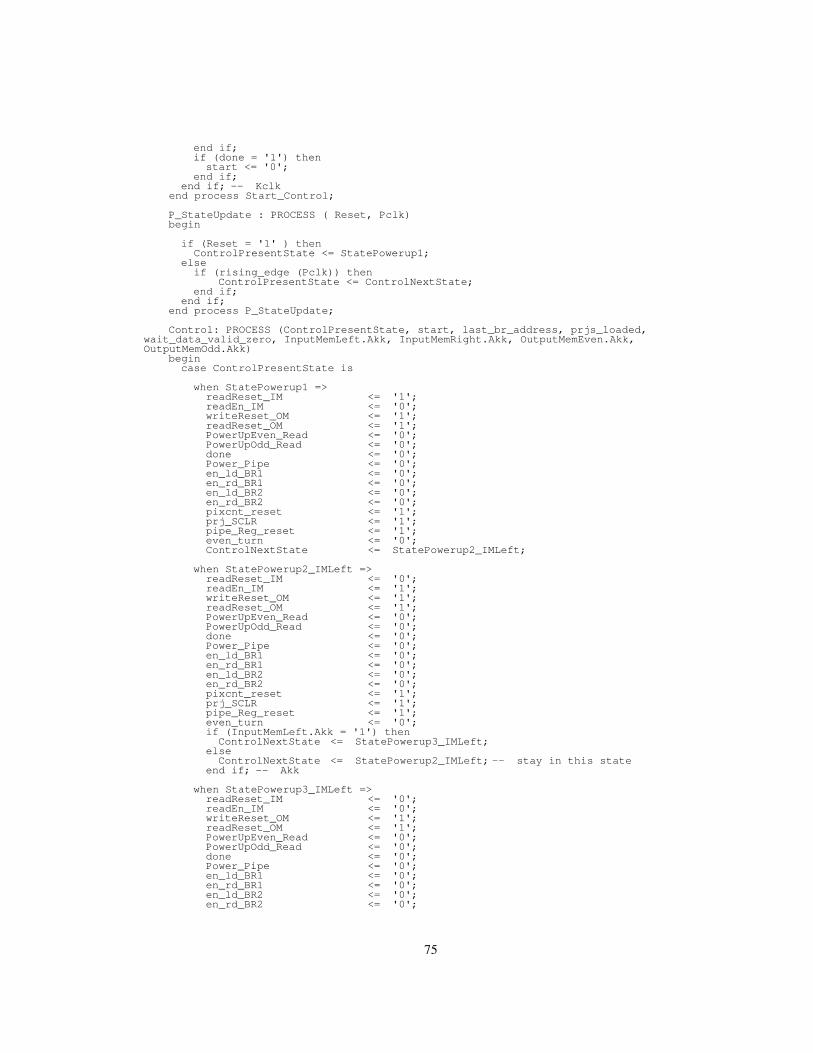
75
end if; if (done = '1') then start <= '0'; end if; end if; -- Kclk end process Start_Control; P_StateUpdate : PROCESS ( Reset, Pclk) begin if (Reset = '1' ) then ControlPresentState <= StatePowerup1; else if (rising_edge (Pclk)) then ControlPresentState <= ControlNextState; end if; end if; end process P_StateUpdate; Control: PROCESS (ControlPresentState, start, last_br_address, prjs_loaded, wait_data_valid_zero, InputMemLeft.Akk, InputMemRight.Akk, OutputMemEven.Akk, OutputMemOdd.Akk) begin case ControlPresentState is when StatePowerup1 => readReset_IM <= '1'; readEn_IM <= '0'; writeReset_OM <= '1'; readReset_OM <= '1'; PowerUpEven_Read <= '0'; PowerUpOdd_Read <= '0'; done <= '0'; Power_Pipe <= '0'; en_ld_BR1 <= '0'; en_rd_BR1 <= '0'; en_ld_BR2 <= '0'; en_rd_BR2 <= '0'; pixcnt_reset <= '1'; prj_SCLR <= '1'; pipe_Reg_reset <= '1'; even_turn <= '0'; ControlNextState <= StatePowerup2_IMLeft; when StatePowerup2_IMLeft => readReset_IM <= '0'; readEn_IM <= '1'; writeReset_OM <= '1'; readReset_OM <= '1'; PowerUpEven_Read <= '0'; PowerUpOdd_Read <= '0'; done <= '0'; Power_Pipe <= '0'; en_ld_BR1 <= '0'; en_rd_BR1 <= '0'; en_ld_BR2 <= '0'; en_rd_BR2 <= '0'; pixcnt_reset <= '1'; prj_SCLR <= '1'; pipe_Reg_reset <= '1'; even_turn <= '0'; if (InputMemLeft.Akk = '1') then ControlNextState <= StatePowerup3_IMLeft; else ControlNextState <= StatePowerup2_IMLeft; -- stay in this state end if; -- Akk when StatePowerup3_IMLeft => readReset_IM <= '0'; readEn_IM <= '0'; writeReset_OM <= '1'; readReset_OM <= '1'; PowerUpEven_Read <= '0'; PowerUpOdd_Read <= '0'; done <= '0'; Power_Pipe <= '0'; en_ld_BR1 <= '0'; en_rd_BR1 <= '0'; en_ld_BR2 <= '0'; en_rd_BR2 <= '0';

76
pixcnt_reset <= '0'; prj_SCLR <= '0'; pipe_Reg_reset <= '1'; even_turn <= '0'; ControlNextState <= StatePowerup2_IMRight; when StatePowerup2_IMRight => readReset_IM <= '0'; readEn_IM <= '1'; writeReset_OM <= '1'; readReset_OM <= '1'; PowerUpEven_Read <= '0'; PowerUpOdd_Read <= '0'; done <= '0'; Power_Pipe <= '0'; en_ld_BR1 <= '0'; en_rd_BR1 <= '0'; en_ld_BR2 <= '0'; en_rd_BR2 <= '0'; pixcnt_reset <= '1'; prj_SCLR <= '1'; pipe_Reg_reset <= '1'; even_turn <= '0'; if (InputMemRight.Akk = '1') then ControlNextState <= StatePowerup3_IMRight; else ControlNextState <= StatePowerup2_IMRight; -- stay in this state end if; -- Akk when StatePowerup3_IMRight => readReset_IM <= '0'; readEn_IM <= '0'; writeReset_OM <= '1'; readReset_OM <= '1'; PowerUpEven_Read <= '0'; PowerUpOdd_Read <= '0'; done <= '0'; Power_Pipe <= '0'; en_ld_BR1 <= '0'; en_rd_BR1 <= '0'; en_ld_BR2 <= '0'; en_rd_BR2 <= '0'; pixcnt_reset <= '0'; prj_SCLR <= '0'; pipe_Reg_reset <= '1'; even_turn <= '0'; ControlNextState <= StatePowerup2_OMEven; when StatePowerup2_OMEven => readReset_IM <= '1'; readEn_IM <= '0'; -- don't enable memory read writeReset_OM <= '0'; readReset_OM <= '1'; PowerUpEven_Read <= '1'; PowerUpOdd_Read <= '0'; done <= '0'; -- not done processing yet Power_Pipe <= '0'; en_ld_BR1 <= '0'; en_rd_BR1 <= '0'; en_ld_BR2 <= '0'; en_rd_BR2 <= '0'; pixcnt_reset <= '1'; prj_SCLR <= '1'; pipe_Reg_reset <= '1'; even_turn <= '1'; if (OutputMemEven.Akk = '1') then ControlNextState <= StatePowerup3_OMEven; else ControlNextState <= StatePowerup2_OMEven; -- stay in this state end if; -- Akk when StatePowerup3_OMEven => readReset_IM <= '1'; readEn_IM <= '0'; -- don't enable memory read writeReset_OM <= '1'; readReset_OM <= '1'; PowerUpEven_Read <= '0'; PowerUpOdd_Read <= '0'; done <= '0'; -- not done processing yet Power_Pipe <= '0';
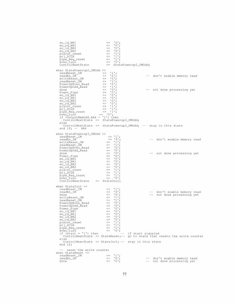
77
en_ld_BR1 <= '0'; en_rd_BR1 <= '0'; en_ld_BR2 <= '0'; en_rd_BR2 <= '0'; pixcnt_reset <= '1'; prj_SCLR <= '1'; pipe_Reg_reset <= '1'; even_turn <= '0'; ControlNextState <= StatePowerup2_OMOdd; when StatePowerup2_OMOdd => readReset_IM <= '1'; readEn_IM <= '0'; -- don't enable memory read writeReset_OM <= '0'; readReset_OM <= '1'; PowerUpEven_Read <= '0'; PowerUpOdd_Read <= '1'; done <= '0'; -- not done processing yet Power_Pipe <= '0'; en_ld_BR1 <= '0'; en_rd_BR1 <= '0'; en_ld_BR2 <= '0'; en_rd_BR2 <= '0'; pixcnt_reset <= '1'; prj_SCLR <= '1'; pipe_Reg_reset <= '1'; even_turn <= '0'; if (OutputMemOdd.Akk = '1') then ControlNextState <= StatePowerup3_OMOdd; else ControlNextState <= StatePowerup2_OMOdd; -- stay in this state end if; -- Akk when StatePowerup3_OMOdd => readReset_IM <= '1'; readEn_IM <= '0'; -- don't enable memory read writeReset_OM <= '1'; readReset_OM <= '1'; PowerUpEven_Read <= '0'; PowerUpOdd_Read <= '0'; done <= '0'; -- not done processing yet Power_Pipe <= '0'; en_ld_BR1 <= '0'; en_rd_BR1 <= '0'; en_ld_BR2 <= '0'; en_rd_BR2 <= '0'; pixcnt_reset <= '1'; prj_SCLR <= '1'; pipe_Reg_reset <= '1'; even_turn <= '0'; ControlNextState <= StateInit; when StateInit => readReset_IM <= '1'; readEn_IM <= '0'; -- don't enable memory read done <= '0'; -- not done processing yet writeReset_OM <= '1'; readReset_OM <= '1'; PowerUpEven_Read <= '0'; PowerUpOdd_Read <= '0'; Power_Pipe <= '0'; en_ld_BR1 <= '0'; en_rd_BR1 <= '0'; en_ld_BR2 <= '0'; en_rd_BR2 <= '0'; pixcnt_reset <= '1'; prj_SCLR <= '1'; pipe_Reg_reset <= '1'; even_turn <= '0'; if (start = '1') then -- if start signaled ControlNextState <= StateReset;-- go to state that resets the write counter else ControlNextState <= StateInit; -- stay in this state end if; -- reset the write counter when StateReset => readReset_IM <= '1'; readEn_IM <= '0'; -- don't enable memory read done <= '0'; -- not done processing yet

78
writeReset_OM <= '1'; readReset_OM <= '1'; PowerUpEven_Read <= '0'; PowerUpOdd_Read <= '0'; Power_Pipe <= '0'; en_ld_BR1 <= '0'; en_rd_BR1 <= '0'; en_ld_BR2 <= '0'; en_rd_BR2 <= '0'; pixcnt_reset <= '1'; prj_SCLR <= '1'; pipe_Reg_reset <= '1'; even_turn <= '0'; ControlNextState <= StateStart; -- go to state that starts processing -- signal the memory read to start when StateStart => readReset_IM <= '0'; readEn_IM <= '1'; -- enable memory read done <= '0'; -- not done processing yet writeReset_OM <= '1'; readReset_OM <= '1'; PowerUpEven_Read <= '0'; PowerUpOdd_Read <= '0'; Power_Pipe <= '0'; en_ld_BR1 <= '1'; en_rd_BR1 <= '0'; en_ld_BR2 <= '0'; en_rd_BR2 <= '0'; pixcnt_reset <= '1'; prj_SCLR <= '1'; pipe_Reg_reset <= '1'; even_turn <= '0'; if (last_br_address = '1') then -- if the memory read has started ControlNextState <= StateWait; -- go to the state that waits for processing to finish else ControlNextState <= StateStart; -- stay in this state end if; -- wait for processing to finish when StateWait => readReset_IM <= '0'; readEn_IM <= '0'; done <= '0'; -- not done processing yet writeReset_OM <= '1'; readReset_OM <= '0'; PowerUpEven_Read <= '0'; PowerUpOdd_Read <= '0'; Power_Pipe <= '1'; en_ld_BR1 <= '0'; en_rd_BR1 <= '0'; en_ld_BR2 <= '0'; en_rd_BR2 <= '0'; pixcnt_reset <= '1'; prj_SCLR <= '1'; pipe_Reg_reset <= '1'; even_turn <= '0'; ControlNextState <= StatePipe1; -- go to the state that signals that the processing is done -- signal that the processing is done -- signal the memory read to start when StatePipe1 => readReset_IM <= '0'; readEn_IM <= '1'; -- enable memory read done <= '0'; -- not done processing yet writeReset_OM <= '0'; readReset_OM <= '0'; PowerUpEven_Read <= '1'; PowerUpOdd_Read <= '0'; Power_Pipe <= '1'; en_ld_BR1 <= '0'; en_rd_BR1 <= '1'; en_ld_BR2 <= '1'; en_rd_BR2 <= '0'; pixcnt_reset <= '0'; prj_SCLR <= '0'; pipe_Reg_reset <= '0'; even_turn <= '1'; if (last_br_address = '1') then -- if the memory read has started

79
ControlNextState <= StatePipe2; -- go to the state that waits for processing to finish else ControlNextState <= StatePipe1; -- stay in this state end if; when StatePipe2 => readReset_IM <= '0'; readEn_IM <= '0'; -- enable memory read done <= '0'; -- not done processing yet writeReset_OM <= '0'; readReset_OM <= '0'; PowerUpEven_Read <= '0'; PowerUpOdd_Read <= '0'; Power_Pipe <= '1'; en_ld_BR1 <= '0'; en_rd_BR1 <= '1'; en_ld_BR2 <= '0'; en_rd_BR2 <= '0'; pixcnt_reset <= '0'; prj_SCLR <= '0'; pipe_Reg_reset <= '0'; even_turn <= '1'; if ((wait_data_valid_zero='1') AND (NOT (prjs_loaded= '1'))) then -- if the memory read has started ControlNextState <= StatePipe3; -- go to the state that waits for processing to finish elsif ((wait_data_valid_zero='1') AND (prjs_loaded= '1')) then ControlNextState <= StatePipe_last; -- stay in this state else ControlNextState <= StatePipe2; -- stay in this state end if; when StatePipe3 => readReset_IM <= '0'; readEn_IM <= '1'; -- enable memory read done <= '0'; -- not done processing yet writeReset_OM <= '0'; readReset_OM <= '0'; PowerUpEven_Read <= '0'; PowerUpOdd_Read <= '0'; Power_Pipe <= '1'; en_ld_BR1 <= '1'; en_rd_BR1 <= '0'; en_ld_BR2 <= '0'; en_rd_BR2 <= '1'; pixcnt_reset <= '0'; prj_SCLR <= '0'; pipe_Reg_reset <= '0'; even_turn <= '0'; if (last_br_address = '0') then -- if the memory read has started ControlNextState <= StatePipe3; -- go to the state that waits for processing to finish else ControlNextState <= StatePipe4; -- stay in this state end if; when StatePipe4 => readReset_IM <= '0'; readEn_IM <= '0'; -- enable memory read writeReset_OM <= '0'; readReset_OM <= '0'; PowerUpEven_Read <= '0'; PowerUpOdd_Read <= '0'; done <= '0'; -- not done processing yet Power_Pipe <= '1'; en_ld_BR1 <= '0'; en_rd_BR1 <= '0'; en_ld_BR2 <= '0'; en_rd_BR2 <= '1'; pixcnt_reset <= '0'; prj_SCLR <= '0'; pipe_Reg_reset <= '0'; even_turn <= '0'; if ((wait_data_valid_zero='1') AND (NOT (prjs_loaded= '1'))) then -- if the memory read has started ControlNextState <= StatePipe1; -- go to the state that waits for processing to finish elsif ((wait_data_valid_zero='1') AND (prjs_loaded= '1')) then ControlNextState <= StatePipe_last; -- stay in this state

80
else ControlNextState <= StatePipe4; -- stay in this state end if; when StatePipe_last => readReset_IM <= '0'; readEn_IM <= '0'; -- enable memory read writeReset_OM <= '0'; readReset_OM <= '0'; PowerUpEven_Read <= '0'; PowerUpOdd_Read <= '0'; done <= '0'; -- not done processing yet Power_Pipe <= '1'; en_ld_BR1 <= '0'; en_rd_BR1 <= '0'; en_ld_BR2 <= '0'; en_rd_BR2 <= '1'; pixcnt_reset <= '0'; prj_SCLR <= '0'; pipe_Reg_reset <= '0'; even_turn <= '0'; if (wait_data_valid_zero = '1') then ControlNextState <= StateEnd; else ControlNextState <= StatePipe_last; end if; when StateEnd => readReset_IM <= '1'; readEn_IM <= '0'; -- don't enable memory read writeReset_OM <= '1'; readReset_OM <= '1'; PowerUpEven_Read <= '0'; PowerUpOdd_Read <= '0'; done <= '1'; -- signal that processing is done Power_Pipe <= '0'; en_ld_BR1 <= '0'; en_rd_BR1 <= '0'; en_ld_BR2 <= '0'; en_rd_BR2 <= '0'; pixcnt_reset <= '0'; prj_SCLR <= '0'; pipe_Reg_reset <= '1'; even_turn <= '0'; if (start = '0') then -- if the register file recieved the signal ControlNextState <= StateInit; -- go to state that waits for start signal else ControlNextState <= StateEnd; -- stay in this state end if; -- go to init be default. should never happen when others => ControlNextState <= StateInit; readReset_IM <= '0'; readEn_IM <= '0'; writeReset_OM <= '0'; readReset_OM <= '0'; PowerUpEven_Read <= '0'; PowerUpOdd_Read <= '0'; done <= '0'; Power_Pipe <= '0'; en_ld_BR1 <= '0'; en_rd_BR1 <= '0'; en_ld_BR2 <= '0'; en_rd_BR2 <= '0'; pixcnt_reset <= '0'; prj_SCLR <= '0'; pipe_Reg_reset <= '0'; even_turn <= '0'; end case; end process Control; pipe_update : process(PCLK, Power_Pipe) BEGIN if(Power_Pipe = '0') then PipePresentState <= PipeInit; else if(rising_edge(PCLK)) then PipePresentState <= PipeNextState; end if;

81
end if; end process pipe_update; pipe_control: process(PipePresentState,current_prj_done) begin case PipePresentState is when PipeInit => pipe1 <= '0'; pipe2 <= '0'; pipe3 <= '0'; pipe4 <= '0'; pipe5 <= '0'; pipe6 <= '0'; pipe7 <= '0'; pipe8 <= '0'; pipe9 <= '0'; pipe10 <= '0'; PipeNextState <= PipeStage1_fill; when PipeStage1_fill => pipe1 <= '1'; pipe2 <= '0'; pipe3 <= '0'; pipe4 <= '0'; pipe5 <= '0'; pipe6 <= '0'; pipe7 <= '0'; pipe8 <= '0'; pipe9 <= '0'; pipe10 <= '0'; PipeNextState <= PipeStage2_fill; when PipeStage2_fill => pipe1 <= '1'; pipe2 <= '1'; pipe3 <= '0'; pipe4 <= '0'; pipe5 <= '0'; pipe6 <= '0'; pipe7 <= '0'; pipe8 <= '0'; pipe9 <= '0'; pipe10 <= '0'; PipeNextState <= PipeStage3_fill; when PipeStage3_fill => pipe1 <= '1'; pipe2 <= '1'; pipe3 <= '1'; pipe4 <= '0'; pipe5 <= '0'; pipe6 <= '0'; pipe7 <= '0'; pipe8 <= '0'; pipe9 <= '0'; pipe10 <= '0'; PipeNextState <= PipeStage4_fill; when PipeStage4_fill => pipe1 <= '1'; pipe2 <= '1'; pipe3 <= '1'; pipe4 <= '1'; pipe5 <= '0'; pipe6 <= '0'; pipe7 <= '0'; pipe8 <= '0'; pipe9 <= '0'; pipe10 <= '0'; PipeNextState <= PipeStage5_fill; when PipeStage5_fill => pipe1 <= '1'; pipe2 <= '1'; pipe3 <= '1'; pipe4 <= '1'; pipe5 <= '1'; pipe6 <= '0'; pipe7 <= '0';

82
pipe8 <= '0'; pipe9 <= '0'; pipe10 <= '0'; PipeNextState <= PipeStage6_fill; when PipeStage6_fill => pipe1 <= '1'; pipe2 <= '1'; pipe3 <= '1'; pipe4 <= '1'; pipe5 <= '1'; pipe6 <= '1'; pipe7 <= '0'; pipe8 <= '0'; pipe9 <= '0'; pipe10 <= '0'; PipeNextState <= PipeStage7_fill; when PipeStage7_fill => pipe1 <= '1'; pipe2 <= '1'; pipe3 <= '1'; pipe4 <= '1'; pipe5 <= '1'; pipe6 <= '1'; pipe7 <= '1'; pipe8 <= '0'; pipe9 <= '0'; pipe10 <= '0'; PipeNextState <= PipeStage8_fill; when PipeStage8_fill => pipe1 <= '1'; pipe2 <= '1'; pipe3 <= '1'; pipe4 <= '1'; pipe5 <= '1'; pipe6 <= '1'; pipe7 <= '1'; pipe8 <= '1'; pipe9 <= '1'; pipe10 <= '1'; if(current_prj_done = '1') then PipeNextState <= PipeStage1_empty; else PipeNextState <= PipeStage8_fill; end if; when PipeStage1_empty => pipe1 <= '0'; pipe2 <= '1'; pipe3 <= '1'; pipe4 <= '1'; pipe5 <= '1'; pipe6 <= '1'; pipe7 <= '1'; pipe8 <= '1'; pipe9 <= '1'; pipe10 <= '1'; PipeNextState <= PipeStage2_empty; when PipeStage2_empty => pipe1 <= '0'; pipe2 <= '0'; pipe3 <= '1'; pipe4 <= '1'; pipe5 <= '1'; pipe6 <= '1'; pipe7 <= '1'; pipe8 <= '1'; pipe9 <= '1'; pipe10 <= '1'; PipeNextState <= PipeStage3_empty; when PipeStage3_empty => pipe1 <= '0'; pipe2 <= '0'; pipe3 <= '0'; pipe4 <= '1'; pipe5 <= '1';

83
pipe6 <= '1'; pipe7 <= '1'; pipe8 <= '1'; pipe9 <= '1'; PipeNextState <= PipeStage4_empty; when PipeStage4_empty => pipe1 <= '0'; pipe2 <= '0'; pipe3 <= '0'; pipe4 <= '0'; pipe5 <= '1'; pipe6 <= '1'; pipe7 <= '1'; pipe8 <= '1'; pipe9 <= '1'; pipe10 <= '1'; PipeNextState <= PipeStage5_empty; when PipeStage5_empty => pipe1 <= '0'; pipe2 <= '0'; pipe3 <= '0'; pipe4 <= '0'; pipe5 <= '0'; pipe6 <= '1'; pipe7 <= '1'; pipe8 <= '1'; pipe9 <= '1'; pipe10 <= '1'; PipeNextState <= PipeStage6_empty; when PipeStage6_empty => pipe1 <= '0'; pipe2 <= '0'; pipe3 <= '0'; pipe4 <= '0'; pipe5 <= '0'; pipe6 <= '0'; pipe7 <= '1'; pipe8 <= '1'; pipe9 <= '1'; pipe10 <= '1'; PipeNextState <= PipeStage7_empty; when PipeStage7_empty => pipe1 <= '0'; pipe2 <= '0'; pipe3 <= '0'; pipe4 <= '0'; pipe5 <= '0'; pipe6 <= '0'; pipe7 <= '0'; pipe8 <= '1'; pipe9 <= '1'; pipe10 <= '1'; PipeNextState <= PipeStage8_empty; when PipeStage8_empty => pipe1 <= '0'; pipe2 <= '0'; pipe3 <= '0'; pipe4 <= '0'; pipe5 <= '0'; pipe6 <= '0'; pipe7 <= '0'; pipe8 <= '0'; pipe9 <= '1'; pipe10 <= '1'; PipeNextState <= PipeStage9_empty; when PipeStage9_empty => pipe1 <= '0'; pipe2 <= '0'; pipe3 <= '0'; pipe4 <= '0'; pipe5 <= '0'; pipe6 <= '0'; pipe7 <= '0'; pipe8 <= '0';

84
pipe9 <= '0'; pipe10 <= '1'; PipeNextState <= PipeStage1_fill; when others => pipe1 <= '0'; pipe2 <= '0'; pipe3 <= '0'; pipe4 <= '0'; pipe5 <= '0'; pipe6 <= '0'; pipe7 <= '0'; pipe8 <= '0'; pipe9 <= '0'; PipeNextState <= PipeInit; end case; end process pipe_control; -------------------------------------------------------------- -------------------------------------------------------------- stall<='1' when (pipe7 = '1' and OutputMem_reg2_dout(25) = '0') else '0'; -------------------------------------------------------------- wait_data_valid_zero <= (not pipe9) and pipe10; -------------------------------------------------------------- --stall <= '0'; --wait_data_valid_zero <= (not pipe8) and pipe9; --****************************************************************************** -- STAGE 1 --****************************************************************************** Pixel_counter: process (Pclk, u_en_pixel_counter,pixel_counter_reset) begin if(rising_edge(Pclk)) then if(pixel_counter_reset = '1') then current_pixel_addr(17 downto 0) <= (17 downto 0 => '0'); else if(u_en_pixel_counter = '1') then current_pixel_addr <= current_pixel_addr + '1'; end if; end if; end if; end process Pixel_counter; -------------------------------------------------------------- -------------------------------------------------------------- -- Control signal related to pixel_counter. pixel_counter_reset <= '1' when pixcnt_reset='1' else (not pipe1); u_en_pixel_counter <= Pipe1 and not stall; current_prj_done <= last_pixel; -- last_pixel <= '1' when (current_pixel_addr(11 downto 0) = (11 downto 0 => '1')) else '0'; -- pixel_zero <= '1' when (current_pixel_addr(11 downto 0) = (11 downto 0 => '0')) else '0'; -- new_row <= '1' when (current_pixel_addr(8 downto 0) = (8 downto 0 => '0')) else '0'; last_pixel <= '1' when (current_pixel_addr(17 downto 0) = (17 downto 0 => '1')) else '0'; pixel_zero <= '1' when (current_pixel_addr(17 downto 0) = (17 downto 0 => '0')) else '0'; new_row <= '1' when (current_pixel_addr(8 downto 0) = (8 downto 0 => '0')) else '0'; -------------------------------------------------------------- u_prj_counter : prj_counter_w6 port map ( Q => prj_num, CLK => PCLK, CE => u_prj_counter_ce, SCLR => prj_SCLR); -------------------------------------------------------------- -------------------------------------------------------------- -- Control signals for u_prj_counter; u_prj_counter_ce <= last_pixel; -------------------------------------------------------------- u_lut1_1 : lut1_1 port map ( A => prj_num, CLK => PCLK, QSPO => lut1_dout(1)); -------------------------------------------------------------- u_lut1_2 : lut1_2 port map (

85
A => prj_num, CLK => PCLK, QSPO => lut1_dout(2)); -------------------------------------------------------------- u_lut1_3 : lut1_3 port map ( A => prj_num, CLK => PCLK, QSPO => lut1_dout(3)); -------------------------------------------------------------- u_lut1_4 : lut1_4 port map ( A => prj_num, CLK => PCLK, QSPO => lut1_dout(4)); -------------------------------------------------------------- u_lut1_5 : lut1_5 port map ( A => prj_num, CLK => PCLK, QSPO => lut1_dout(5)); -------------------------------------------------------------- u_lut1_6 : lut1_6 port map ( A => prj_num, CLK => PCLK, QSPO => lut1_dout(6)); -------------------------------------------------------------- u_lut1_7 : lut1_7 port map ( A => prj_num, CLK => PCLK, QSPO => lut1_dout(7)); -------------------------------------------------------------- u_lut1_8 : lut1_8 port map ( A => prj_num, CLK => PCLK, QSPO => lut1_dout(8)); -------------------------------------------------------------- -------------------------------------------------------------- u_lut1_9 : lut1_9 port map ( A => prj_num, CLK => PCLK, QSPO => lut1_dout(9)); -------------------------------------------------------------- u_lut1_10 : lut1_10 port map ( A => prj_num, CLK => PCLK, QSPO => lut1_dout(10)); -------------------------------------------------------------- u_lut1_11 : lut1_11 port map ( A => prj_num, CLK => PCLK, QSPO => lut1_dout(11)); -------------------------------------------------------------- u_lut1_12 : lut1_12 port map ( A => prj_num, CLK => PCLK, QSPO => lut1_dout(12)); -------------------------------------------------------------- u_lut1_13 : lut1_13 port map ( A => prj_num, CLK => PCLK, QSPO => lut1_dout(13)); -------------------------------------------------------------- u_lut1_14 : lut1_14 port map ( A => prj_num, CLK => PCLK, QSPO => lut1_dout(14)); -------------------------------------------------------------- u_lut1_15 : lut1_15 port map ( A => prj_num,
86
CLK => PCLK, QSPO => lut1_dout(15)); -------------------------------------------------------------- u_lut1_16 : lut1_16 port map ( A => prj_num, CLK => PCLK, QSPO => lut1_dout(16)); -------------------------------------------------------------- u_lut2_1 : lut2_1 port map ( A => prj_num, CLK => PCLK, QSPO => lut2_dout(1)); -------------------------------------------------------------- u_lut2_2 : lut2_2 port map ( A => prj_num, CLK => PCLK, QSPO => lut2_dout(2)); -------------------------------------------------------------- u_lut2_3 : lut2_3 port map ( A => prj_num, CLK => PCLK, QSPO => lut2_dout(3)); -------------------------------------------------------------- u_lut2_4 : lut2_4 port map ( A => prj_num, CLK => PCLK, QSPO => lut2_dout(4)); -------------------------------------------------------------- u_lut2_5 : lut2_5 port map ( A => prj_num, CLK => PCLK, QSPO => lut2_dout(5)); -------------------------------------------------------------- u_lut2_6 : lut2_6 port map ( A => prj_num, CLK => PCLK, QSPO => lut2_dout(6)); -------------------------------------------------------------- u_lut2_7 : lut2_7 port map ( A => prj_num, CLK => PCLK, QSPO => lut2_dout(7)); -------------------------------------------------------------- u_lut2_8 : lut2_8 port map ( A => prj_num, CLK => PCLK, QSPO => lut2_dout(8)); -------------------------------------------------------------- u_lut2_9 : lut2_9 port map ( A => prj_num, CLK => PCLK, QSPO => lut2_dout(9)); -------------------------------------------------------------- u_lut2_10 : lut2_10 port map ( A => prj_num, CLK => PCLK, QSPO => lut2_dout(10)); -------------------------------------------------------------- u_lut2_11 : lut2_11 port map ( A => prj_num, CLK => PCLK, QSPO => lut2_dout(11)); -------------------------------------------------------------- u_lut2_12 : lut2_12 port map ( A => prj_num, CLK => PCLK, QSPO => lut2_dout(12));

87
-------------------------------------------------------------- u_lut2_13 : lut2_13 port map ( A => prj_num, CLK => PCLK, QSPO => lut2_dout(13)); -------------------------------------------------------------- u_lut2_14 : lut2_14 port map ( A => prj_num, CLK => PCLK, QSPO => lut2_dout(14)); -------------------------------------------------------------- u_lut2_15 : lut2_15 port map ( A => prj_num, CLK => PCLK, QSPO => lut2_dout(15)); -------------------------------------------------------------- u_lut2_16 : lut2_16 port map ( A => prj_num, CLK => PCLK, QSPO => lut2_dout(16)); -------------------------------------------------------------- u_lut3_1 : lut3_1 port map ( A => prj_num, CLK => PCLK, QSPO => lut3_dout(1)); -------------------------------------------------------------- u_lut3_2 : lut3_2 port map ( A => prj_num, CLK => PCLK, QSPO => lut3_dout(2)); -------------------------------------------------------------- u_lut3_3 : lut3_3 port map ( A => prj_num, CLK => PCLK, QSPO => lut3_dout(3)); -------------------------------------------------------------- u_lut3_4 : lut3_4 port map ( A => prj_num, CLK => PCLK, QSPO => lut3_dout(4)); -------------------------------------------------------------- u_lut3_5 : lut3_5 port map ( A => prj_num, CLK => PCLK, QSPO => lut3_dout(5)); -------------------------------------------------------------- u_lut3_6 : lut3_6 port map ( A => prj_num, CLK => PCLK, QSPO => lut3_dout(6)); -------------------------------------------------------------- u_lut3_7 : lut3_7 port map ( A => prj_num, CLK => PCLK, QSPO => lut3_dout(7)); -------------------------------------------------------------- u_lut3_8 : lut3_8 port map ( A => prj_num, CLK => PCLK, QSPO => lut3_dout(8)); -------------------------------------------------------------- u_lut3_9 : lut3_9 port map ( A => prj_num, CLK => PCLK, QSPO => lut3_dout(9)); -------------------------------------------------------------- u_lut3_10 : lut3_10

88
port map ( A => prj_num, CLK => PCLK, QSPO => lut3_dout(10)); -------------------------------------------------------------- u_lut3_11 : lut3_11 port map ( A => prj_num, CLK => PCLK, QSPO => lut3_dout(11)); -------------------------------------------------------------- u_lut3_12 : lut3_12 port map ( A => prj_num, CLK => PCLK, QSPO => lut3_dout(12)); -------------------------------------------------------------- u_lut3_13 : lut3_13 port map ( A => prj_num, CLK => PCLK, QSPO => lut3_dout(13)); -------------------------------------------------------------- u_lut3_14 : lut3_14 port map ( A => prj_num, CLK => PCLK, QSPO => lut3_dout(14)); -------------------------------------------------------------- u_lut3_15 : lut3_15 port map ( A => prj_num, CLK => PCLK, QSPO => lut3_dout(15)); -------------------------------------------------------------- u_lut3_16 : lut3_16 port map ( A => prj_num, CLK => PCLK, QSPO => lut3_dout(16)); -------------------------------------------------------------- --****************************************************************************** -- STAGE 2 --****************************************************************************** u_pipe_stage2_mux: FOR i IN 1 TO 16 GENERATE pipe_stage2_mux_O(i) <= pipe_stage2_subtracter_Q(i) when u_pipe_stage2_mux_S = '0' else (lut1_dout(i)&"0000000000"); END GENERATE; -------------------------------------------------------------- -------------------------------------------------------------- u_pipe_stage2_mux_S <= pipe_reg1_pixel_zero; pipe_reg1_pixel_zero <= pixel_zero when rising_edge(Pclk); -------------------------------------------------------------- stage2_subtracter: FOR i IN 1 TO 16 GENERATE u_pipe_stage2_subtracter : subtracter_w25u_w16u port map ( A => pipe_stage2_mux_O(i), B => lut2_dout(i), Q => pipe_stage2_subtracter_Q(i), CLK => PCLK, CE => u_pipe_stage2_subtracter_ce, ACLR => pipe_reg_reset); END GENERATE; -------------------------------------------------------------- -------------------------------------------------------------- u_pipe_stage2_subtracter_ce <= not stall and new_row; pipe_reg1_new_row <= new_row when rising_edge(Pclk); -------------------------------------------------------------- --****************************************************************************** -- STAGE 3 --****************************************************************************** u_pipe_stage3_mux: FOR i IN 1 TO 16 GENERATE pipe_stage3_mux_O(i) <= pipe_stage3_adder_Q(i)(24 downto 0) when u_pipe_stage3_mux_S='0' else pipe_stage2_subtracter_Q(i); END GENERATE; --------------------------------------------------------------- --------------------------------------------------------------- u_pipe_stage3_mux_S <= pipe_reg1_new_row;

89
--------------------------------------------------------------- stage3_adder: FOR i IN 1 TO 16 GENERATE u_pipe_stage3_adder : adder_w26s_w17s port map ( A => pipe_stage3_adder_A(i), B => lut3_dout(i), Q => pipe_stage3_adder_Q(i), CLK => PCLK, CE => u_pipe_stage3_adder_ce, ACLR => pipe_reg_reset); END GENERATE; --------------------------------------------------------------- --------------------------------------------------------------- u_pipe_stage3_adder_ce <= pipe2 and not stall; adder_one_bit_suf: FOR i IN 1 TO 16 GENERATE pipe_stage3_adder_A(i) <= '0'&pipe_stage3_mux_O(i); END GENERATE; --------------------------------------------------------------- --****************************************************************************** -- STAGE 4 --****************************************************************************** stage4_round: FOR i IN 1 TO 16 GENERATE u_Round_unsigned: Round_unsigned generic map ( total_data_width => 5 ) port map ( data_in => pipe_stage3_adder_Q(i)(14 DOWNTO 10), data_out => pipe_stage4_round_out(i) ); END GENERATE; --------------------------------------------------------------- stage4_demux: FOR i IN 1 TO 16 GENERATE u_demux: address_demux generic map ( address_width => 10 ) port map ( address_in => pipe_stage3_adder_Q(i)(24 downto 15), address_out_even => even_addr(i), address_out_odd => odd_addr(i) ); END GENERATE; --------------------------------------------------------------- ifactor_reg4: FOR i IN 1 TO 16 GENERATE u_pipe_reg4_ifactor : reg_w4 port map ( D => pipe_stage4_round_out(i), Q => pipe_reg4_ifactor(i), CLK => PCLK, CE => u_pipe_reg4_ifactor_ce, ACLR => pipe_reg_reset); END GENERATE; --------------------------------------------------------------- --------------------------------------------------------------- u_pipe_reg4_ifactor_ce <= pipe3 and not stall; --------------------------------------------------------------- lsb: FOR i IN 1 TO 16 GENERATE u_pipe_reg4_lsb(i) <= '0' when (pipe_reg_reset='1') else ((pipe_stage3_adder_Q(i)(15) and not stall) or (u_pipe_reg4_lsb(i) and stall)) when rising_edge(PCLK) else (u_pipe_reg4_lsb(i)) when rising_edge(PCLK); END GENERATE; --------------------------------------------------------------------------------------- prjs_loaded <= '1' when (prj_num(5 downto 0) = prj_to_process(5 downto 0)) else '0'; --------------------------------------------------------------------------------------- --****************************************************************************** -- INPUT MEMORY CONTROL (Sinogram loading) --******************************************************************************

90
ReadCntr_IML: process (MClk,readReset_IM,readEn_IM,InputMemLeft.Akk,readDone_IML,readAddr_IML) variable case_var :unsigned(3 downto 0); begin case_var :=(readReset_IM, ReadEn_IM,InputMemLeft.Akk,readDone_IML); InputMemLeft.Addr <= readAddr_IML; InputMemLeft.Write <= '0'; if (rising_edge(MClk)) then case case_var is when "0000" => InputMemLeft.Req <= '0'; InputMemLeft.Low_Enable <= '0'; InputMemLeft.High_enable <= '0'; when "0001" => readDone_IML <= '0'; InputMemLeft.Req <= '0'; InputMemLeft.Low_Enable <= '0'; InputMemLeft.High_enable <= '0'; when "0010" => InputMemLeft.Req <= '0'; InputMemLeft.Low_Enable <= '0'; InputMemLeft.High_enable <= '0'; when "0011" => readDone_IML <= '0'; InputMemLeft.Req <= '0'; InputMemLeft.Low_Enable <= '0'; InputMemLeft.High_enable <= '0'; when "0100" => InputMemLeft.Req <= '1'; InputMemLeft.Low_Enable <= '1'; InputMemLeft.High_enable <= '1'; when "0101" => InputMemLeft.Req <= '0'; InputMemLeft.Low_Enable <= '0'; InputMemLeft.High_enable <= '0'; when "0110" => if(readAddr_IML(10 downto 0) = (10 downto 0 => '1')) then readDone_IML <='1'; InputMemLeft.Req <= '0'; InputMemLeft.Low_Enable <= '0'; InputMemLeft.High_enable <= '0'; else InputMemLeft.Req <= '1'; InputMemLeft.Low_Enable <= '1'; InputMemLeft.High_enable <= '1'; end if; readAddr_IML <= readAddr_IML + '1'; when "0111" => InputMemLeft.Req <= '0'; InputMemLeft.Low_Enable <= '0'; InputMemLeft.High_enable <= '0'; when others => --reset readin memory InputMemLeft.Req <= '0'; InputMemLeft.Low_Enable <= '0'; InputMemLeft.High_enable <= '0'; readDone_IML <= '0'; readAddr_IML <= (others => '0'); end case; end if; end process ReadCntr_IML; ReadCntr_IMR: process (MClk,readReset_IM,readEn_IM,InputMemRight.Akk,readDone_IMR,readAddr_IMR) variable case_var :unsigned(3 downto 0); begin case_var :=(readReset_IM, ReadEn_IM,InputMemRight.Akk,readDone_IMR); InputMemRight.Addr <= readAddr_IMR; InputMemRight.Write <= '0';

91
if (rising_edge(MClk)) then case case_var is when "0000" => InputMemRight.Req <= '0'; InputMemRight.Low_Enable <= '0'; InputMemRight.High_enable <= '0'; when "0001" => readDone_IMR <= '0'; InputMemRight.Req <= '0'; InputMemRight.Low_Enable <= '0'; InputMemRight.High_enable <= '0'; when "0010" => InputMemRight.Req <= '0'; InputMemRight.Low_Enable <= '0'; InputMemRight.High_enable <= '0'; when "0011" => readDone_IMR <= '0'; InputMemRight.Req <= '0'; InputMemRight.Low_Enable <= '0'; InputMemRight.High_enable <= '0'; when "0100" => InputMemRight.Req <= '1'; InputMemRight.Low_Enable <= '1'; InputMemRight.High_enable <= '1'; when "0101" => InputMemRight.Req <= '0'; InputMemRight.Low_Enable <= '0'; InputMemRight.High_enable <= '0'; when "0110" => if(readAddr_IMR(10 downto 0) = (10 downto 0 => '1')) then readDone_IMR <='1'; InputMemRight.Req <= '0'; InputMemRight.Low_Enable <= '0'; InputMemRight.High_enable <= '0'; else InputMemRight.Req <= '1'; InputMemRight.Low_Enable <= '1'; InputMemRight.High_enable <= '1'; end if; readAddr_IMR <= readAddr_IMR + '1'; when "0111" => InputMemRight.Req <= '0'; InputMemRight.Low_Enable <= '0'; InputMemRight.High_enable <= '0'; when others => --reset readin memory InputMemRight.Req <= '0'; InputMemRight.Low_Enable <= '0'; InputMemRight.High_enable <= '0'; readDone_IMR <= '0'; readAddr_IMR <= (others => '0'); end case; end if; end process ReadCntr_IMR; ----------------------------------------------------------------------------- BR_address_counter_even : counter_w11 port map ( Q => BR_address_even, CLK => PCLK, THRESH0 => last_br_address_even, CE => InputMemLeft.Low_Data_Valid, ACLR => readReset_IM); ------------------------------------------------------------------------------- BR_address_counter_odd : counter_w11 port map ( Q => BR_address_odd, CLK => PCLK, THRESH0 => last_br_address_odd, CE => InputMemRight.Low_Data_Valid, ACLR => readReset_IM);

92
------------------------------------------------------------------------------- last_br_address <= last_br_address_even or last_br_address_odd; -- last_br_address <= last_br_address_even and last_br_address_odd; blockram_group1: FOR i IN 1 TO 4 GENERATE Even_1 : block_ram_dual_port port map ( addra => BR_address_even(8 downto 0), addrb => even_addr(i), clka => PCLK, clkb => PCLK, dina => dina_e(i), doutb => doutb_e1(i), ena => en_ld_BR1, enb => u_blkram1_rd_ce, wea => wea_1); ----------------------------------------------------- Odd_1 : block_ram_dual_port port map ( addra => BR_address_odd(8 downto 0), addrb => odd_addr(i), clka => PCLK, clkb => PCLK, dina => dina_o(i), doutb => doutb_o1(i), ena => en_ld_BR1, enb => u_blkram1_rd_ce, wea => wea_2); ----------------------------------------------------- Even_2 : block_ram_dual_port port map ( addra => BR_address_even(8 downto 0), addrb => even_addr(i), clka => PCLK, clkb => PCLK, dina => dina_e(i), doutb => doutb_e2(i), ena => en_ld_BR2, enb => u_blkram2_rd_ce, wea => wea_1); ----------------------------------------------------- Odd_2 : block_ram_dual_port port map ( addra => BR_address_odd(8 downto 0), addrb => odd_addr(i), clka => PCLK, clkb => PCLK, dina => dina_o(i), doutb => doutb_o2(i), ena => en_ld_BR2, enb => u_blkram2_rd_ce, wea => wea_2); END GENERATE; blockram_group2: FOR i IN 1 TO 4 GENERATE Even_3 : block_ram_dual_port port map ( addra => BR_address_even(8 downto 0), addrb => even_addr(i+4), clka => PCLK, clkb => PCLK, dina => dina_e(i), doutb => doutb_e1(i+4), ena => en_ld_BR1, enb => u_blkram1_rd_ce, wea => wea_3); ----------------------------------------------------- Odd_3 : block_ram_dual_port port map ( addra => BR_address_odd(8 downto 0), addrb => odd_addr(i+4), clka => PCLK, clkb => PCLK, dina => dina_o(i), doutb => doutb_o1(i+4), ena => en_ld_BR1, enb => u_blkram1_rd_ce,

93
wea => wea_4); ----------------------------------------------------- Even_4 : block_ram_dual_port port map ( addra => BR_address_even(8 downto 0), addrb => even_addr(i+4), clka => PCLK, clkb => PCLK, dina => dina_e(i), doutb => doutb_e2(i+4), ena => en_ld_BR2, enb => u_blkram2_rd_ce, wea => wea_3); ----------------------------------------------------- Odd_4 : block_ram_dual_port port map ( addra => BR_address_odd(8 downto 0), addrb => odd_addr(i+4), clka => PCLK, clkb => PCLK, dina => dina_o(i), doutb => doutb_o2(i+4), ena => en_ld_BR2, enb => u_blkram2_rd_ce, wea => wea_4); END GENERATE; blockram_group3: FOR i IN 1 TO 4 GENERATE Even_5 : block_ram_dual_port port map ( addra => BR_address_even(8 downto 0), addrb => even_addr(i+8), clka => PCLK, clkb => PCLK, dina => dina_e(i), doutb => doutb_e1(i+8), ena => en_ld_BR1, enb => u_blkram1_rd_ce, wea => wea_5); ----------------------------------------------------- Odd_5 : block_ram_dual_port port map ( addra => BR_address_odd(8 downto 0), addrb => odd_addr(i+8), clka => PCLK, clkb => PCLK, dina => dina_o(i), doutb => doutb_o1(i+8), ena => en_ld_BR1, enb => u_blkram1_rd_ce, wea => wea_6); ----------------------------------------------------- Even_6 : block_ram_dual_port port map ( addra => BR_address_even(8 downto 0), addrb => even_addr(i+8), clka => PCLK, clkb => PCLK, dina => dina_e(i), doutb => doutb_e2(i+8), ena => en_ld_BR2, enb => u_blkram2_rd_ce, wea => wea_5); ----------------------------------------------------- Odd_6 : block_ram_dual_port port map ( addra => BR_address_odd(8 downto 0), addrb => odd_addr(i+8), clka => PCLK, clkb => PCLK, dina => dina_o(i), doutb => doutb_o2(i+8), ena => en_ld_BR2, enb => u_blkram2_rd_ce, wea => wea_6);

94
END GENERATE; blockram_group4: FOR i IN 1 TO 4 GENERATE Even_7 : block_ram_dual_port port map ( addra => BR_address_even(8 downto 0), addrb => even_addr(i+12), clka => PCLK, clkb => PCLK, dina => dina_e(i), doutb => doutb_e1(i+12), ena => en_ld_BR1, enb => u_blkram1_rd_ce, wea => wea_7); ----------------------------------------------------- Odd_7 : block_ram_dual_port port map ( addra => BR_address_odd(8 downto 0), addrb => odd_addr(i+12), clka => PCLK, clkb => PCLK, dina => dina_o(i), doutb => doutb_o1(i+12), ena => en_ld_BR1, enb => u_blkram1_rd_ce, wea => wea_8); ----------------------------------------------------- Even_8 : block_ram_dual_port port map ( addra => BR_address_even(8 downto 0), addrb => even_addr(i+12), clka => PCLK, clkb => PCLK, dina => dina_e(i), doutb => doutb_e2(i+12), ena => en_ld_BR2, enb => u_blkram2_rd_ce, wea => wea_7); ----------------------------------------------------- Odd_8 : block_ram_dual_port port map ( addra => BR_address_odd(8 downto 0), addrb => odd_addr(i+12), clka => PCLK, clkb => PCLK, dina => dina_o(i), doutb => doutb_o2(i+12), ena => en_ld_BR2, enb => u_blkram2_rd_ce, wea => wea_8); END GENERATE; --------------------------------------------------- u_blkram1_rd_ce <= en_rd_BR1 and not stall; u_blkram2_rd_ce <= en_rd_BR2 and not stall; blockram_input: FOR i IN 1 TO 4 GENERATE dina_e(i)<=InputMemLeft.Data_in(35-(i-1)*9 downto 27-(i-1)*9); dina_o(i)<=InputMemRight.Data_in(35-(i-1)*9 downto 27-(i-1)*9); -- dina_e(i)<=InputMemLeft.Data_in(i*9-1 downto (i-1)*9); -- dina_o(i)<=InputMemRight.Data_in(i*9-1 downto (i-1)*9); END GENERATE; wea_1<=InputMemLeft.High_Data_Valid AND InputMemLeft.Low_Data_Valid and (not BR_address_even(10) and not BR_address_even(9)); wea_2<=InputMemRight.High_Data_Valid AND InputMemRight.Low_Data_Valid and (not BR_address_odd(10) and not BR_address_odd(9)); wea_3<=InputMemLeft.High_Data_Valid AND InputMemLeft.Low_Data_Valid and (not BR_address_even(10) and BR_address_even(9)); wea_4<=InputMemRight.High_Data_Valid AND InputMemRight.Low_Data_Valid and (not BR_address_odd(10) and BR_address_odd(9)); wea_5<=InputMemLeft.High_Data_Valid AND InputMemLeft.Low_Data_Valid and (BR_address_even(10) and not BR_address_even(9)); wea_6<=InputMemRight.High_Data_Valid AND InputMemRight.Low_Data_Valid and (BR_address_odd(10) and not BR_address_odd(9)); wea_7<=InputMemLeft.High_Data_Valid AND InputMemLeft.Low_Data_Valid and (BR_address_even(10) and BR_address_even(9));

95
wea_8<=InputMemRight.High_Data_Valid AND InputMemRight.Low_Data_Valid and (BR_address_odd(10) and BR_address_odd(9)); -- wea_8<=InputMemRight.High_Data_Valid AND InputMemRight.Low_Data_Valid and (BR_address_even(10) and BR_address_even(9)); ----------------------------------------------------- --****************************************************************************** -- STAGE 5 --****************************************************************************** ram_selector_even: FOR i IN 1 TO 16 GENERATE dout_even(i) <= doutb_e1(i) when en_rd_BR2 = '0' else doutb_e2(i); END GENERATE; ram_selector_odd: FOR i IN 1 TO 16 GENERATE dout_odd(i) <= doutb_o1(i) when en_rd_BR2 = '0' else doutb_o2(i); END GENERATE; data_swap: FOR i IN 1 TO 16 GENERATE out_a(i) <= dout_odd(i) when u_pipe_reg4_lsb(i) = '0' else dout_even(i); out_b(i) <= dout_even(i) when u_pipe_reg4_lsb(i) = '0' else dout_odd(i); END GENERATE; stage5_subtractor: FOR i IN 1 TO 16 GENERATE u_interpolation_subtractor : subtractor_w9s_w9s port map ( A => out_a(i), B => out_b(i), Q => interpolation_sub_Q(i), CLK => PCLK, CE => u_interpolation_sub_ce, ACLR => pipe_reg_reset); END GENERATE; ----------------------------------------------------- ----------------------------------------------------- u_interpolation_sub_ce <= pipe4 and not stall; ----------------------------------------------------- ifactor_reg5: FOR i IN 1 TO 16 GENERATE u_pipe_reg5_ifactor : reg_w4 port map ( D => pipe_reg4_ifactor(i), Q => pipe_reg5_ifactor(i), CLK => PCLK, CE => u_pipe_reg5_ifactor_ce, ACLR => pipe_reg_reset); END GENERATE; ----------------------------------------------------- ----------------------------------------------------- u_pipe_reg5_ifactor_ce <= pipe4 and not stall; ----------------------------------------------------- reg5_switch_out_b: FOR i IN 1 TO 16 GENERATE u_pipe_reg5_switch_out_b : reg_w9 port map ( D => out_b(i), Q => pipe_reg5_switch_out_b(i), CLK => PCLK, CE => u_pipe_reg5_switch_out_b_ce, ACLR => pipe_reg_reset); END GENERATE; ----------------------------------------------------- ----------------------------------------------------- u_pipe_reg5_switch_out_b_ce <= pipe4 and not stall; ----------------------------------------------------- --****************************************************************************** -- STAGE 6 --****************************************************************************** stage6_mult: FOR i IN 1 TO 16 GENERATE u_mult : multiplier_w10s_w4u port map ( clk => Pclk, a => interpolation_sub_Q(i), b => pipe_reg5_ifactor(i), q => interpolation_mult_Q(i), ce => u_multiplier_ce, aclr => pipe_reg_reset); END GENERATE; ----------------------------------------------------- ----------------------------------------------------- u_multiplier_ce <= pipe5 and not stall; ----------------------------------------------------- reg6_switch_out_b: FOR i IN 1 TO 16 GENERATE

96
u_pipe_reg6_switch_out_b : reg_w9 port map ( D => pipe_reg5_switch_out_b(i), Q => pipe_reg6_switch_out_b(i), CLK => PCLK, CE => u_pipe_reg6_switch_out_b_ce, ACLR => pipe_reg_reset); END GENERATE; ----------------------------------------------------- ----------------------------------------------------- u_pipe_reg6_switch_out_b_ce <= pipe5 and not stall; ----------------------------------------------------- --****************************************************************************** -- STAGE 7 --****************************************************************************** ----------------------------------------------------- reg6_suffix_4b: FOR i IN 1 TO 16 GENERATE pipe_reg6_switch_out_b_sr4(i) <= pipe_reg6_switch_out_b(i) & "0000"; END GENERATE; ----------------------------------------------------- intrp_adder: FOR i IN 1 TO 16 GENERATE u_intrp_adder : interpolation_adder_noreg port map ( A => interpolation_mult_Q(i), B => pipe_reg6_switch_out_b_sr4(i), S => intrp_adder_S(i)); END GENERATE; ----------------------------------------------------- interm1_adder: FOR i IN 1 TO 8 GENERATE u_interm1_adder : interm_adder_15s_15s_noreg port map ( A => intrp_adder_S(2*i-1), B => intrp_adder_S(2*i), S => interm1_adder_Q(i)); END GENERATE; ----------------------------------------------------- interm2_adder: FOR i IN 1 TO 4 GENERATE u_interm2_adder : interm_adder_16s_16s port map ( A => interm1_adder_Q(2*i-1), B => interm1_adder_Q(2*i), Q => interm2_adder_Q(i), CLK => PCLK, CE => u_interm2_adder_ce, ACLR => pipe_reg_reset); END GENERATE; ----------------------------------------------------- ----------------------------------------------------- u_interm2_adder_ce <= pipe6 and not stall; ----------------------------------------------------- --****************************************************************************** -- STAGE 8 --****************************************************************************** interm3_adder: FOR i IN 1 TO 2 GENERATE u_interm3_adder: interm_adder_17s_17s_noreg port map ( A => interm2_adder_Q(2*i-1), B => interm2_adder_Q(2*i), S => interm3_adder_Q(i)); END GENERATE; ----------------------------------------------------- u_interm4_adder: interm_adder_18s_18s_noreg port map ( A => interm3_adder_Q(1), B => interm3_adder_Q(2), S => interm4_adder_Q); ----------------------------------------------------- u_prj_acc_adder : adder_w19s_w25s port map ( A => interm4_adder_Q, B => OutputMem_reg2_dout(24 downto 0), Q => pixel_value_Q, CLK => PCLK, CE => u_prj_acc_adder_ce, ACLR => pipe_reg_reset); ----------------------------------------------------- ----------------------------------------------------- u_prj_acc_adder_ce <= pipe7 and not stall;

97
----------------------------------------------------- --****************************************************************************** -- Output Memory Control (Accumulation) --****************************************************************************** OutputMemOdd.Data_Out(31 DOWNTO 25) <=(OTHERS => '0'); OutputMemOdd.Data_Out(24 DOWNTO 0) <=pixel_value_Q when even_turn='1' else (24 downto 0 => '0'); OutputMemEven.Data_Out(31 DOWNTO 25) <=(OTHERS => '0'); OutputMemEven.Data_Out(24 DOWNTO 0) <=pixel_value_Q when even_turn='0' else (24 downto 0 => '0'); OutputMem_ctrl: process(Mclk,writeReset_OM,wait_data_valid_zero) begin if(wait_data_valid_zero = '1' or writeReset_OM = '1') then -- initialize both output memory address to zero. OutputMemOdd.Addr <= (others => '0'); OutputMemOdd.Req <= '0'; OutputMemOdd.Low_Enable <= '0'; OutputMemOdd.Write <= '0'; OutputMemEven.Addr <= (others => '0'); OutputMemEven.Req <= '0'; OutputMemEven.Low_Enable <= '0'; OutputMemEven.Write <= '0'; current_prj_read_done <= '0'; delayed <= '0'; elsif(rising_edge(Mclk)) then -- read from one memory and write to the other memory according to flag "even_turn". if(even_turn = '1') then -- read from even memory and write to odd memory. if(current_prj_read_done = '0') then OutputMemEven.Req <='1'; OutputMemEven.Low_enable <= '1'; OutputMemEven.Write <= '0'; if(OutputMemEven.Akk = '1') then OutputMemEven.Addr <= OutputMemEven.Addr + '1'; end if; if(OutputMemEven.Addr(17 downto 0) = (17 downto 0 => '1')) then current_prj_read_done <= '1'; end if; else OutputMemEven.Req <='0'; OutputMemEven.Low_enable <= '0'; OutputMemEven.Write <= '0'; end if; if(pipe7 = '1' and OutputMem_reg2_dout(25)='1') then if(delayed = '1') then OutputMemOdd.Req <= '1'; OutputMemOdd.Low_enable <= '1'; OutputMemOdd.Write <= '1'; if(OutputMemOdd.Akk <= '1') then OutputMemOdd.Addr <= OutputMemOdd.Addr + '1'; end if; else delayed <= '1'; OutputMemOdd.Req <= '1'; OutputMemOdd.Low_enable <= '1'; OutputMemOdd.Write <= '1'; end if; end if; end if; -- even turn. if(even_turn = '0') then -- read from even memory and write to odd memory. if(current_prj_read_done = '0') then OutputMemOdd.Req <='1'; OutputMemOdd.Low_enable <= '1'; OutputMemOdd.Write <= '0'; if(OutputMemOdd.Akk = '1') then OutputMemOdd.Addr <= OutputMemOdd.Addr + '1'; end if; if(OutputMemOdd.Addr(17 downto 0) = (17 downto 0 => '1')) then current_prj_read_done <= '1'; end if; else OutputMemOdd.Req <='0'; OutputMemOdd.Low_enable <= '0';

98
OutputMemOdd.Write <= '0'; end if; if(pipe7 = '1' and OutputMem_reg2_dout(25)='1') then if(delayed = '1') then OutputMemEven.Req <= '1'; OutputMemEven.Low_enable <= '1'; OutputMemEven.Write <= '1'; if(OutputMemEven.Akk <= '1') then OutputMemEven.Addr <= OutputMemEven.Addr + '1'; end if; -- OutputMemOdd.Akk else delayed <= '1'; OutputMemEven.Req <= '1'; OutputMemEven.Low_enable <= '1'; OutputMemEven.Write <= '1'; end if; end if; --Pipe7 and OutputMem_reg2_dout(25) end if; -- odd turn end if; -- wait_data_valid_zero or writeReset_OM end process OutputMem_ctrl; ----------------------------------------------------- OutputMem_reg1_din <= OutputMemEven.Low_Data_Valid & OutputMemEven.Data_in(24 downto 0) when even_turn='1' else OutputMemOdd.Low_Data_Valid & OutputMemOdd.Data_in(24 downto 0); ----------------------------------------------------- u_OutputMem_reg1 : reg_w26 port map ( D => OutputMem_reg1_din, Q => OutputMem_reg1_dout, CLK => PCLK, ACLR => pipe_reg_reset); ----------------------------------------------------- u_OutputMem_reg2 : reg_w26 port map ( D => OutputMem_reg1_dout, Q => OutputMem_reg2_dout, CLK => PCLK, ACLR => pipe_reg_reset); ------------------------------------------------------- END behavioral;