Nonlinear response of a ballistic graphene transistor with ...
15
PHYSICAL REVIEW B 94, 125445 (2016) Nonlinear response of a ballistic graphene transistor with an ac-driven gate: High harmonic generation and terahertz detection Y. Korniyenko, 1 O. Shevtsov, 2 and T. L¨ ofwander 1 1 Department of Microtechnology and Nanoscience - MC2, Chalmers University of Technology, SE-412 96 G¨ oteborg, Sweden 2 Department of Physics & Astronomy, Northwestern University, Evanston, Illinois 60208, USA (Received 14 July 2016; published 30 September 2016) We present results for time-dependent electron transport in a ballistic graphene field-effect transistor with an ac-driven gate. Nonlinear response to the ac drive is derived utilizing Floquet theory for scattering states in combination with Landauer-B¨ uttiker theory for transport. We identify two regimes that can be useful for applications: (i) low and (ii) high doping of graphene under source and drain contacts, relative to the doping level in the graphene channel, which in an experiment can be varied by a back gate. In both regimes, inelastic scattering induced by the ac drive can excite quasibound states in the channel that leads to resonance promotion of higher-order sidebands. Already for weak to intermediate ac drive strength, this leads to a substantial change in the direct current between source and drain. For strong ac drive with frequency , we compute the higher harmonics of frequencies n (n integer) in the source-drain conductance. In regime (ii), we show that particular harmonics (for instance, n = 6) can be selectively enhanced by tuning the doping level in the channel or by tuning the drive strength. We propose that the device operated in the weak-drive regime can be used to detect THz radiation, while in the strong-drive regime, it can be used as a frequency multiplier. DOI: 10.1103/PhysRevB.94.125445 I. INTRODUCTION Graphene for analog high-frequency electronics has been the focus of intense research over the last few years, and is one of the focus areas in the recently published graphene road map [1]. Two dimensionality of the material, high carrier mobility, gate-tunable charge density, and a unique band structure with massless Dirac electrons are a few of the properties that make graphene a promising material in this context [2–6]. Examples of devices already produced, with competitive figures of merit, are field-effect transistors [7], frequency doublers [8], frequency mixers [9], and detectors [10–13]. The electronic mobility has been constantly improving and ballistic electron transport is today studied intensively. Ballistic transport allows for development of massless Dirac electron optics, which is the graphene analog of usual optics. Electron optics effects that have been observed include Fabry- P´ erot interferences and snake states [14], Veselago lensing [15], and so-called whispering gallery modes in circular p-n junctions [16]. For ballistic devices, evidence of hydrodynamic behavior has been recently presented: viscous electron backflow [17] and breakdown of the Wideman-Franz law [18,19]. This indicates that due to the long elastic mean free path, and slow electron-phonon relaxation below room temperature, electron- electron interactions can be the most dominant scattering channel within a certain temperature window. However, at sufficiently low temperatures (below 100 K), electron-electron interactions also become weak and, ultimately, at lower temperature, transport is truly ballistic over long (μm) length scales. Improved mobility (possibly reaching ballistic transport) is a necessary condition for the development of high-frequency devices. There has therefore been a broad interest in the theory of time-dependent transport in graphene in the ballistic transport regime, including quantum pumping [20–23], non- linear electromagnetic response [24–33], and photon-assisted tunneling [34–40]. In the nonclassical regime, when the energy scale , set by the drive frequency ( is Planck’s constant divided by 2π ), and the Fermi energy E F , measured relative to the charge-neutrality point, are of comparable magnitude, a variety of interesting quantum mechanical interference and resonance effects become important. In a recent paper [41], we have studied in detail a Fano resonance [38–40,42] induced by a quasibound state on the top-gate barrier. We showed how it could be utilized to develop a frequency doubler for weak or moderate ac drive strength. In this paper, we extend this study to include a more realistic doping profile across the device as well as strong ac drive. Within a fully quantum mechanical treatment based on Floquet theory and Landauer-B¨ uttiker scattering theory [42–45], we show how Fano resonances as well as resonant tunneling can be utilized for detection of high-frequency radiation in the THz range or to generate high harmonics of the ac signal. The outline of the paper is as follows. In Sec. II, we give details of the model and the methods of calculations. This section also includes a characterization of the dc regime as a prologue to the discussions of time-dependent transport in the following chapter, as well as a detailed discussion of the relation between the different parameters of the model and various possible transport regimes. In Sec. III, we present results for the weak ac drive regime, with focus on high- frequency radiation detection. In Sec. IV, we present the result for the strong ac drive regime, with focus on high harmonic generation. Section V summarizes the paper. A few technical results are collected in the Appendix. II. MODEL Our goal is to establish a relation between intrinsic electronic transport properties of a ballistic graphene transistor, depicted in Fig. 1(a), and experimentally controllable physi- cal parameters. Extrinsic (parasitic) effects due to eventual 2469-9950/2016/94(12)/125445(15) 125445-1 ©2016 American Physical Society
Transcript of Nonlinear response of a ballistic graphene transistor with ...

PHYSICAL REVIEW B 94, 125445 (2016)
Nonlinear response of a ballistic graphene transistor with an ac-driven gate:High harmonic generation and terahertz detection
Y. Korniyenko,1 O. Shevtsov,2 and T. Lofwander1
1Department of Microtechnology and Nanoscience - MC2, Chalmers University of Technology, SE-412 96 Goteborg, Sweden2Department of Physics & Astronomy, Northwestern University, Evanston, Illinois 60208, USA
(Received 14 July 2016; published 30 September 2016)
We present results for time-dependent electron transport in a ballistic graphene field-effect transistor withan ac-driven gate. Nonlinear response to the ac drive is derived utilizing Floquet theory for scattering statesin combination with Landauer-Buttiker theory for transport. We identify two regimes that can be useful forapplications: (i) low and (ii) high doping of graphene under source and drain contacts, relative to the dopinglevel in the graphene channel, which in an experiment can be varied by a back gate. In both regimes, inelasticscattering induced by the ac drive can excite quasibound states in the channel that leads to resonance promotionof higher-order sidebands. Already for weak to intermediate ac drive strength, this leads to a substantial changein the direct current between source and drain. For strong ac drive with frequency �, we compute the higherharmonics of frequencies n� (n integer) in the source-drain conductance. In regime (ii), we show that particularharmonics (for instance, n = 6) can be selectively enhanced by tuning the doping level in the channel or bytuning the drive strength. We propose that the device operated in the weak-drive regime can be used to detectTHz radiation, while in the strong-drive regime, it can be used as a frequency multiplier.
DOI: 10.1103/PhysRevB.94.125445
I. INTRODUCTION
Graphene for analog high-frequency electronics has beenthe focus of intense research over the last few years, and is oneof the focus areas in the recently published graphene road map[1]. Two dimensionality of the material, high carrier mobility,gate-tunable charge density, and a unique band structure withmassless Dirac electrons are a few of the properties that makegraphene a promising material in this context [2–6]. Examplesof devices already produced, with competitive figures ofmerit, are field-effect transistors [7], frequency doublers [8],frequency mixers [9], and detectors [10–13].
The electronic mobility has been constantly improvingand ballistic electron transport is today studied intensively.Ballistic transport allows for development of massless Diracelectron optics, which is the graphene analog of usual optics.Electron optics effects that have been observed include Fabry-Perot interferences and snake states [14], Veselago lensing[15], and so-called whispering gallery modes in circular p-njunctions [16].
For ballistic devices, evidence of hydrodynamic behaviorhas been recently presented: viscous electron backflow [17]and breakdown of the Wideman-Franz law [18,19]. Thisindicates that due to the long elastic mean free path, and slowelectron-phonon relaxation below room temperature, electron-electron interactions can be the most dominant scatteringchannel within a certain temperature window. However, atsufficiently low temperatures (below 100 K), electron-electroninteractions also become weak and, ultimately, at lowertemperature, transport is truly ballistic over long (μm) lengthscales.
Improved mobility (possibly reaching ballistic transport) isa necessary condition for the development of high-frequencydevices. There has therefore been a broad interest in thetheory of time-dependent transport in graphene in the ballistictransport regime, including quantum pumping [20–23], non-linear electromagnetic response [24–33], and photon-assisted
tunneling [34–40]. In the nonclassical regime, when the energyscale ��, set by the drive frequency � (� is Planck’s constantdivided by 2π ), and the Fermi energy EF , measured relativeto the charge-neutrality point, are of comparable magnitude,a variety of interesting quantum mechanical interference andresonance effects become important. In a recent paper [41], wehave studied in detail a Fano resonance [38–40,42] induced bya quasibound state on the top-gate barrier. We showed how itcould be utilized to develop a frequency doubler for weak ormoderate ac drive strength. In this paper, we extend this studyto include a more realistic doping profile across the device aswell as strong ac drive. Within a fully quantum mechanicaltreatment based on Floquet theory and Landauer-Buttikerscattering theory [42–45], we show how Fano resonances aswell as resonant tunneling can be utilized for detection ofhigh-frequency radiation in the THz range or to generate highharmonics of the ac signal.
The outline of the paper is as follows. In Sec. II, we givedetails of the model and the methods of calculations. Thissection also includes a characterization of the dc regime asa prologue to the discussions of time-dependent transport inthe following chapter, as well as a detailed discussion of therelation between the different parameters of the model andvarious possible transport regimes. In Sec. III, we presentresults for the weak ac drive regime, with focus on high-frequency radiation detection. In Sec. IV, we present the resultfor the strong ac drive regime, with focus on high harmonicgeneration. Section V summarizes the paper. A few technicalresults are collected in the Appendix.
II. MODEL
Our goal is to establish a relation between intrinsicelectronic transport properties of a ballistic graphene transistor,depicted in Fig. 1(a), and experimentally controllable physi-cal parameters. Extrinsic (parasitic) effects due to eventual
2469-9950/2016/94(12)/125445(15) 125445-1 ©2016 American Physical Society

Y. KORNIYENKO, O. SHEVTSOV, AND T. LOFWANDER PHYSICAL REVIEW B 94, 125445 (2016)
FIG. 1. (a) Schematics of a graphene field-effect transistor, wherea back gate (BG) controls doping of the channel, and a smallsource-drain (S-D) bias is applied to generate the current, whichis controlled by the top-gate (TG) dc and ac signals. (b) Potentiallandscape, including doping of the leads by the source and drainmetallic electrodes.
surrounding circuit elements must be dealt with when doingexperiments, but can be neglected in an attempt to describethe intrinsic properties. We make a minimal model based on anumber of assumptions that we outline in the following.
First, we assume that the contacts and gates are ideal,such that they can be described by the potential landscapesketched in Fig. 1(b). We take into account that the sourceand drain metallic contacts dope graphene underneath dueto work function mismatches. The doping levels, set by UL
and UR , in the graphene source and drain areas are therebypinned [46]. On the other hand, in the transistor channel region,x ∈ [−L1,L2], the doping level can be tuned by the back-gatepotential. We define the channel Dirac point energy by settingED = UC [assuming absence of electron-hole (e-h) puddles],where UC can be tuned by the back gate. Since we measureenergies with respect to the Fermi level EF = 0 (aligned withthe metallic contact Fermi energies), the Dirac point in thechannel region is aligned with the Fermi energy for UC = 0(the channel is then charge neutral). In summary, the dopingprofile sketched in Fig. 1(b) is given by
U (x) = ULθ (−L1 − x) + URθ (x − L2)
+UC[θ (x + L1) − θ (x − L2)]. (1)
We assume that the top gate is wide on the scale of theC-C bond length acc, but short on the scale that the envelopeof the Dirac electron wave function varies, which is givenby λD = �vF /(E − UC), where vF is the Fermi velocity. Forenergies E near the Dirac point in the channel, we haveλD � acc. Based on the same arguments, we assume that thedoping level is changing slowly near the contacts on the acc
scale, but fast on the scale of λD . These assumptions meanthat we can neglect intervalley scattering in the problem and
consider only one valley. For transport quantities, a factortwo for valley degeneracy is included in addition to the factortwo for spin degeneracy. The above assumptions also allowus to use step functions for the doping profile, as in Eq. (1),and a δ barrier model for the top-gate potential. The effectivelow-energy Hamiltonian then has the form
H = −iσx∇x + σyky + [Z0 + Z1 cos(�t)]δ(x) + U (x),
(2)
where we have set the Fermi velocity in graphene equal tounity, vF = 1, and � = 1. The Pauli matrices in pseudospinspace (A-B sublattices) are denoted by σx and σy . We assumethe device to be very wide and translationally invariant alongy. Thus any edge effects are negligibly small and transversemomentum ky is (approximately) conserved. Above, Z0 andZ1 are, respectively, the static and dynamic parts of the driveapplied at the top gate. The δ-function description of the top-gate barrier is obtained as a limiting case of a very high V →∞ and narrow D → 0 square barrier, with the product (barrierstrength) V D = Z constant. Note that this theory for the Diracquasiparticle envelope wave function holds as long as acc �D � λD .
Wave-function solutions have to satisfy the time-dependentDirac equation
Hψ(x,ky,t) = i∂tψ(x,ky,t). (3)
The harmonic potential, with frequency �, in the HamiltonianH in Eq. (2) allows us to use a Fourier decomposition andconstruct a Floquet ansatz,
ψ(x,ky,t) = e−iEt
∞∑n=−∞
ψn(x,ky,E)e−in�t , (4)
where amplitudes at sideband energies En = E + n� (ninteger) are the result of the charge carrier picking up (orgiving up) energy quanta n� from the oscillating barrier. Thequasienergy E is set by the energy of the particle incident fromthe source electrode in the scattering problem. When pluggedinto Eq. (3), it yields a set of coupled differential equations forsideband amplitudes ψn(x,ky,E). The solutions can be derivedin a straightforward manner by wave-function matching andcollected into a Floquet scattering matrix describing scatteringof a quasiparticle incoming from the left or right reservoir atenergy E and transverse momentum ky . We have collectedall the key steps of the derivation in the Appendix. Thereflection amplitudes rn(ky,E) are given in Eq. (B10) and thetransmission amplitudes tn(ky,E) are given in Eq. (B11).
Following the Landauer-Buttiker scattering approach, theFloquet scattering matrix can be used to compute the time-dependent conductance G(t) between source and drain. Theconductance is computed in linear response to the source-drainvoltage VSD , but in nonlinear response to the oscillatingtop-gate potential, described by its drive strength Z1 andfrequency �. The conductance is also a function of the staticpotential landscape, described by U (x), as well as the statictop-gate potential quantified by its barrier strength Z0. Wederived the general formula for G(t) in Ref. [41]. Here wechoose to present results for the linear conductance in theright lead at x = L+
2 , i.e., at the interface with the channelregion. The expression for the conductance (per unit length in
125445-2

NONLINEAR RESPONSE OF A BALLISTIC GRAPHENE . . . PHYSICAL REVIEW B 94, 125445 (2016)
the transverse direction) at zero temperature is then [47]
G(EF ,t) =∞∑
n=−∞Gn(EF )e−in�t , (5)
Gn(EF ) = G∗−n(EF ), (6)
Gn(EF ) = 4e2
h
∫ ∞
−∞
dky
2π
∞∑m=−∞
× η∗(ky,Em − UR) + η(ky,En+m − UR)
2√
v(ky,Em − UR)v(ky,En+m − UR)
× ei[κ(ky ,Em−UR )−κ(ky ,En+m−UR )]×L2
× t†m(ky,E)tn+m(ky,E)|E=EF, (7)
where η(ky,E), v(ky,E), and κ(ky,E) are defined in Eq. (A5).The factor with velocities appears here because we utilizea scattering basis where elementary waves in the leads carryunit probability flux. This guarantees that the scattering matrixcoupling incoming and outgoing waves in the leads is unitary.The phase of the conductance components Gn for n �= 0 isunimportant for our discussion and we will present results for|Gn| below. Note that in the static case (i.e., Z1 = 0), the factorwith velocities as well as the phase factor both reduce to unityand the usual Landauer-Buttiker formula for dc conductancesimply in terms of transmission is obtained.
In the rest of the paper, we shall report results for a symmet-ric setup with L1 = L2 = L/2 and symmetric doping profileUL = UR = U . The transmission probabilities are computedfor zero back-gate voltage, i.e., UC = 0, as a function of energyE and transverse momentum ky = |E − U | sin ϕ parametrizedby an impact angle ϕ. This means that E = 0 corresponds totransmission at the Dirac point in the channel region. This is aconventional way to present transmission through a potentiallandscape. On the other hand, the zero-temperature linearconductance, computed via Eq. (7), shall be presented as afunction of the channel doping UC (the position of the Diracpoint energy ED). In an experiment, the channel doping levelcan be tuned by the back-gate voltage VBG. Since the Fermienergy is pinned to the metallic source and drain contact Fermienergies, the radius of the Dirac cone in the graphene leadsis constant, set by the doping level U , while the radius in thechannel is given by UC and varies with back-gate voltage. Thischoice should correspond to the experimental situation.
A. Dc characteristics
We start by analyzing the static case (Z1 = 0) in order toset the stage for the signatures of the time-dependent drivethat we will study in the following sections. It is usefulto first look at the case with no applied top-gate potentialZ0 = 0, thereby highlighting the effect of the inhomogeneousdoping profile. In fact, U (x) describes a square barrier acrossthe channel of width L = L1 + L2. We plot the transmissionprobability T0(E,ϕ) in Fig. 2(a). The transmission amplitudeis governed by pseudospin matching between regions withdifferent doping. For small angles ϕ, the mismatch is negligiblysmall, thus transmission approaches unity (Klein tunneling).
FIG. 2. (a) Dc transmission probability as a function of energyand incidence angle. Electrodes are doped at U = −10/L, whilethe gate potentials are zero such that Z0 = 0 and UC = 0. Greendashed lines indicate boundaries to evanescent regions |ϕ| > ϕc. (b)Transmission probability in the presence of a top-gate dc potential,Z0 = 0.4π . Blue long-dashed lines indicate resonant tunneling. (c),(d) The connection between evanescent waves at the δ barrier for off-and on-resonance tunneling, respectively.
The peaks in transmission for large angles ϕ and negativeenergies E < −5/L in Fig. 2(a) are analogous to Fabry-Perotfringes, i.e., the result of wave interference between twopartially reflecting mirrors (boundaries at the source and drainin this case). A typical fringe oscillation period is of the order of2π�vf /L (reinstating the units). In addition to the two effectsdescribed above, there is a large region where transmissionis largely suppressed. It occurs when the waves in thechannel region are evanescent. Their longitudinal momentum
component κ(ky,E) = ±√
E2 − k2y turns imaginary, giving us
125445-3

Y. KORNIYENKO, O. SHEVTSOV, AND T. LOFWANDER PHYSICAL REVIEW B 94, 125445 (2016)
a condition on the critical angle of incidence ϕc,
ϕc = arcsin
∣∣∣∣ E
E − U
∣∣∣∣. (8)
For any |ϕ| > ϕc, the waves injected from the electrodes areevanescent in the channel (x ∈ [−L1,L2]). Note that Eq. (8)holds for |E| < |E − U |. Otherwise there are no evanescentwaves involved in transport and we may put ϕc = π/2. Theboundary between propagating wave transport and evanescentwave transport is indicated by a green dashed line in Fig. 2(a).
The evanescent wave factor exp(−√
k2y − E2L) lowers the
transmission probability in general. However, for energiesclose to the Dirac point and small ky (or small L), this factoris still quite large and evanescent waves can reach between thetwo contacts, thus giving rise to large transmission probability.Transport at E = 0 is achieved exclusively through evanescentwaves. This is the so-called pseudodiffusive transport regime[48].
When we introduce the static top-gate δ-barrier potential,Z0 �= 0, additional features appear in the transmission. First,the Fabry-Perot oscillations are shifted due to an additionalphase shift at the δ barrier; see Fig. 2(b). More importantly,the δ barrier can host one bound state at energy
Eb = UC − sgn(Z0)|ky | cos Z0, (9)
which we studied for U (x) = 0 in Ref. [41]. In that case,the bound state does not affect dc transport properties, butcan be excited by ac drive. Here, for finite electrode dopingU �= 0, the bound state can be excited already in dc. In fact,in this case, it is not a true bound state, rather a quasiboundstate with evanescent waves in the channel region connected topropagating waves in the leads. In Fig. 2(b), we see that the res-onance in T0(E,ϕ) originates at E = 0 and then disperses withthe angle of incidence ϕ. The resonance can be understood inanalogy with widely studied resonant double-barrier tunneling[49,50] in Schrodinger quantum mechanics. In the analogy,the two barriers correspond in our case to the two channelregions between the contacts and the top-gate δ barrier, andthe resonant level between the barriers corresponds in our caseto the quasibound state in the δ barrier. A complementary pointof view of the resonance can be found in the equations; seeAppendix A 3. Off resonance, exponentially decaying waveswith amplitudes a and c are connected, as sketched in Fig. 2(c).This results in an exponentially small transmission amplitude.On the other hand, when the quasibound state is hit, theexponentially decaying wave with amplitude a on one side ofthe δ barrier is coupled only to an exponentially rising solutionwith amplitude d on the other side, as sketched in Fig. 2(d).The exponential functions thereby cancel in the expressionfor the transmission which leads to resonance behavior [cf.Eq. (A28)].
For the calculation of the conductance in Eq. (7), we needto integrate the transmission probability over angles. In anattempt to describe the typical experimental situation, weassume that the Fermi energy in the device and the dopinglevels in the leads are pinned by the Fermi energy in the metalcontacts, while the back gate can be used to tune thedoping level in the channel. The zero-temperature conductanceas a function of UC is then computed by integrating the
FIG. 3. (a) Transmission probability in the absence of top-gatebarrier (Z0 = 0) for electrodes with pinned doping levels set byU = −10/L, and varying channel doping level UC , which definesthe position of the Dirac point relative to the Fermi energy EF = 0.(b) The transmission probability including a top-gate barrier ofstrength Z0 = 0.4π . (c) Corresponding angle-integrated dc linearconductances for Z0 = 0 (blue dashed line) and for Z0 = 0.4π (solidblack line).
transmission function T (E,ϕ; UL,UR,UC) over angles at fixedenergy E = 0 (Fermi energy) and fixed UL and UR . We plotthe corresponding view of the angle-dependent transmissionfunction in Figs. 3(a) and 3(b). Note that in Fig. 2, we plottedT (E,ϕ; UL,UR,UC) as a function of E and ϕ for fixed UC = 0and fixed UL and UR . The transmission function as viewed inFigs. 3(a) and 3(b) corresponds to leads that are electron doped(here, U = −10/L). Thus, both incoming waves and scatteredwaves in the leads are electronlike (n type) at the Fermi energyEF = 0. For UC < 0, we have electronlike waves at EF = 0in the channel, while for UC > 0, we have holelike waves inthe channel (p type). Therefore, the Fabry-Perot interferencepatterns for positive UC (n-p-n junction) and negative UC
(n-n′-n junction) are different.In Fig. 3(c), we present the dc conductance as a function
of channel doping level UC . For |UC | < |U |, we have mainly
125445-4

NONLINEAR RESPONSE OF A BALLISTIC GRAPHENE . . . PHYSICAL REVIEW B 94, 125445 (2016)
TABLE I. Energy scales within our model and relevant parame-ters that determine them.
U contact doping levels UR = UL = U
UC channel doping level�vF /L channel length L = L1 + L2
�vF / L channel asymmetry L = |L1 − L2|�� drive frequency �
evanescent mode transport, while for larger values of |UC |,we find oscillations due to the Fabry-Perot interferences. Theresonance peak near UC = 0 (solid black line for finite Z0) isdue to the δ-barrier-induced quasibound state.
B. Parameter regimes
Starting from the dc characterization above, we can identifyseveral parameter regimes. They can be described by differentrelations between the relevant energy scales in the problem,listed in Table I. In the dc characterization above, we used�vF /L as the energy scale. Note that with vF = 1 = �,energies are measured in units of L−1. In addition to therelations between the energy scales in Table I, we have totake into account the oscillating δ-barrier strength Z1.
The observed regimes in dc are (cf. Fig. 3) as follows:(I) |UC | � |U |: propagating wave transport.(a) |U | ∼ �vF /L: clearly visible Fabry-Perot interferences
as a function of UC with period approximately given by2π�vF /L;
(b) |U | � �vF /L: very fast oscillations that in realitywould be washed out by inhomogeneity or temperaturesmearing;
(c) |U | � �vF /L: the oscillations are too slow (on the scaleof UC ∼ U ) to be observed.
(II) |UC | � |U |: evanescent wave transport (pseudodiffu-sive regime).
(a) U � �vF / L: resonant tunneling is possible when thechannel is not too asymmetric.
The dc drive strength Z0 sets the position of the quasiboundstate in the resonant tunneling regime and shifts the Fabry-Perot oscillations, but does not define a regime by itself. Wenote that both the evanescent wave regime [51] and the Fabry-Perot regime [14] have been observed experimentally.
Under the ac drive, we will in the next sections investigatethe following regimes:
(III) Z1 < 1: Weak to intermediate drive.(a) �� � U , low contact doping; with (Ia) above: Fano and
Breit-Wigner resonances;(b) �� < U , high contact doping; with (IIa) above: inelastic
resonant tunneling.(IV) Z1 > 1: Strong drive.(a) �� � U , low contact doping; with (Ia) above: multiple
Fano and Breit-Wigner resonances;(b) �� < U , high contact doping; with (IIa) above: inelastic
resonant tunneling and high harmonic generation.We can estimate from experiments the typical parameter
values. Contact doping (parameter U ) has been reported[52,53] in the range of −100 to 100 meV (correspondingto doping levels of up to 1012 cm−2, either n or p type).
Typical device channel lengths are from 10 nm to 1 μm,making the corresponding energy scale �vf /L in the rangeof 1–100 meV. The corresponding ballistic flight time fromsource to drain is τ = L/vF and is about 1 ps. We notein passing that within Landauer-Buttiker scattering theory,all relaxation times must then be longer than this, which isthe case at low temperature and low energies in a ballisticdevice (mobility μ � 105 cm2/V s). The driving frequency,��, is between 0.4–40 meV for the THz frequency range0.1–10 THz. The drive strength Z1, for Z1 ∼ 1, correspondsto a voltage of the order of a meV on the top gate for typicalgate lengths (see the estimate in our previous paper [41]).Finally, in the following, we assume that temperature is thesmallest energy scale (we put T = 0). With these numbers, allparameter regimes listed above are within experimental reach.
III. WEAK TO INTERMEDIATE DRIVE, Z1 < 1
A. Low contact doping: Fano and Breit-Wigner resonances
In Ref. [41], we studied the case when �vF /L is the smallestenergy scale, i.e., the channel is long. We were then allowedto assume that evanescent waves cannot reach between thecontacts and the δ barrier. In practice, we set U (x) = 0, andlet L → ∞. In these limits, we studied Fano and Breit-Wignerresonances induced by the δ-barrier quasibound state andargued that they can be used to enhance the second harmonic.In the more general formalism introduced here, we can askwhat a small amount of contact doping U �= 0 leads to. Wepresent in Figs. 4(a) and 4(b) the transmission probabilitiesT0(E,ϕ) and T2(E,ϕ) for a small amount of contact doping andlarge distance to contacts, |U | = �vF /L = 0.01�. Comparedwith the results in Ref. [41], we find a small wedge ofevanescent wave transport in an energy window aroundE = 0 (outside the green dashed lines). The transmission ofpropagating waves displays fast Fabry-Perot interferences. TheFano resonance in T0 and the Breit-Wigner resonance in T2
[processes sketched in Fig. 4(c)] are, however, not affected.For increasing contact doping (larger |U |), the Fabry-Perotoscillations get stronger and will eventually interfere withthe Fano and Breit-Wigner resonances, but not destroy them.This holds as long as �vF /L � �. For shorter contacts, thewedge of evanescent wave transport around E = 0 widens.When �vF /L and � are of comparable magnitude, the mostimportant feature in the transmission is instead resonantinelastic tunneling.
B. High contact doping: Inelastic resonant tunnelling
Let us next consider the resonant tunneling regime. Weassume a symmetric device with L1 = L2, with highly dopedleads, and weakly doped channel, |UC | � |U |, such thatwe have evanescent wave transport through the device. Theresonance due to the quasibound state in the δ barrier studiedfor dc transport above will also create resonant inelastictunneling under ac drive. The resonance condition for weakdrive Z1 � 1 is n� = Eb. This leads to promotion of higher-order sidebands as well as higher harmonics in the conductancethat we will study below.
In Fig. 5, we present the transmission probabilities Tn forn = 0, ±1, and 2. For T0 in Fig. 5(a), two new transmission
125445-5

Y. KORNIYENKO, O. SHEVTSOV, AND T. LOFWANDER PHYSICAL REVIEW B 94, 125445 (2016)
FIG. 4. (a) Direct transmission probability T0(E,ϕ) and (b) trans-mission probability to the second sideband T2(E,ϕ) for parameterscorresponding to Fig. 2 in Ref. [41] (Z0 = 0.4π , Z1 = 0.45), butincluding a small doping of contact leads U = −0.01� relative to thechannel (UC = 0). The device is long, such that �vF /L = 0.01�. (c)Sketches of the Fano resonance process and the inelastic Breit-Wignerresonance process identified in Ref. [41] to be responsible for thedip-peak structure in T0 and the peak in T2, respectively.
peaks emerge, separated by ±� from the main (0th) peakpresent already in dc. The side peaks emerge because of thepossibility of absorbing/emitting energy quanta, as shown inFig. 5(b). In the evanescent region, multiple sideband energiescan now satisfy the bound state requirement, thus resultingin a number of resonant peaks separated roughly by � (forZ0 ≈ π/2). Generally, these peaks are weaker than the one inthe static case, since the bound-state contribution is now spreadacross several channels. Analogous processes are involvedduring inelastic scattering between sidebands, as illustratedin Figs. 5(c) and 5(d) for T1, Figs. 5(e) and 5(f) for T−1, andFigs. 5(g) and 5(h) for T2.
In Fig. 6, we present the dc conductance G0 as a functionof channel doping UC for increasing ac drive strength Z1.The inelastic resonant tunneling processes discussed abovefor transmission probabilities result in side peaks in theconductance spaced by multiples of � from the main resonance
FIG. 5. Resonant transmission via evanescent waves for elastictransmission (n = 0) and inelastic transmission to sideband energies(n = ±1 and n = 2). The parameters are U = −10/L, � = 0.45/L,Z0 = 0.5π , and Z1 = 0.1.
peak present in dc. Already for rather weak drive Z0 ∼ 0.1,several peaks are visible and the main elastic peak is reduced.This can be traced to the energy dependence in the matrix onthe left-hand side in Eq. (B11), which is given by a combinationof functions in Eq. (A5), all inversely proportional to energy.The bound-state energy |Eb − UC | is small, which results indivision of small numbers and enhanced effective coupling ofsidebands close to the resonance energy. Thus, the range ofvalidity of a perturbative approach in small Z1 is limited.
In the literature, when systems other than graphene havebeen studied, the conductance is often presented as a functionof ac drive frequency [45]. That is natural since there is oftenno knob corresponding to the very convenient back gate whichcan be used to tune the graphene channel doping level (i.e.,the parameter UC varied above). For comparison, we presentin Fig. 7 the dc conductance for varying frequency, keepingthe doping level UC = 1/L, i.e., a hole-doped channel. In thiscase, we find conductance peaks at frequencies such that asideband coincides with the quasibound state, i.e., n� = Eb.Higher-order processes are weaker for weak drive strength Z1,thus the resonance peaks have smaller amplitudes and widths.
Considering Figs. 6 and 7 together, it is clear that the devicecan be used as a tunable detector. The frequency � of thesignal that needs to be detected tells us which channel dopingwe should choose (tunable by the back gate), such that the first
125445-6

NONLINEAR RESPONSE OF A BALLISTIC GRAPHENE . . . PHYSICAL REVIEW B 94, 125445 (2016)
FIG. 6. (a) Dc conductance under ac drive of varying strength Z1
in a range of channel dopings UC corresponding to evanescent wavetransport. The resonance peak for dc is reduced under ac drive andside peaks spaced by multiples of � appear due to resonant inelastictunneling. (b) Horizontal cuts in the color map in (a) at particularvalues of Z1. The parameters are Z0 = 0.48π , U = −10/L, and� = 0.4/L.
sideband is resonant. Then the dc conductance is monitored todetect the signal.
IV. STRONG DRIVE, Z1 > 1
To understand the system behavior at strong drive, itis useful to look at the transmission probability behavioras a function of driving strength Z1. Since the δ-barrierboundary condition matrix M is directly related to Besselfunctions of the first kind in sideband space [see Eq. (C10)],we can expect transmission amplitudes to also follow thecorresponding Bessel functions. To illustrate the point, weintroduce normalized angle-integrated transmissions,
τn(UC,Z1) =∫
dϕ Tn(ϕ,UC,Z1)∫dϕ T0(ϕ,UC,Z1 = 0)
. (10)
Indeed, the general behavior of τn for constant UC follows thatof J 2
n (Z1); see Fig. 8. Next, let us discuss how the resonancesdescribed above for weak drive evolve for strong drive, bearingin mind that the distribution of sideband amplitudes is insimplified terms given by Bessel functions.
A. Low contact doping
First, we would like to discuss the evolution of Fano andBreit-Wigner resonances described above for low doping U
of contacts. We observe multiple Fano resonances (cf. Fig. 9)that are due to the bound-state condition satisfied by sidebandwaves in the contacts. It is useful to note that since we fixed theenergy EF = 0 and have UC as our parameter, the evanescent
FIG. 7. (a) Dc conductance under varying ac drive frequency� for the same parameters as in Fig. 6, but with fixed channeldoping UC = 1/L. Inelastic tunneling resonance peaks appear whena sideband coincides with the quasibound state.
wave region boundaries for sideband n become horizontallines, given by |ϕ| = φn
c , where
φnc = arcsin
∣∣∣∣n� − U
U
∣∣∣∣. (11)
Note that this equation holds for |n� − U | < |U |. Otherwise,waves are propagating in the contacts for all ϕ and we canset φn
c = π/2. To avoid confusion, we emphasize that φnc in
Eq. (11) defines critical angles for evanescent sideband wavesin the contacts (which do not contribute to transport), whileϕc in Eq. (8) defines a critical angle for evanescent waves inthe channel (which do contribute to transport). For parametersused in Fig. 9, only n = 1 and 2 sidebands have evanescentregions. The corresponding Fano and Breit-Wigner resonances
FIG. 8. Bessel functions envelopes (dashed lines) and normalizedangle-integrated sideband transmissions Tn (solid lines) for UC =−9/L. The parameters are U = −10/L, Z0 = 0.4π , and � = 1/L.
125445-7

Y. KORNIYENKO, O. SHEVTSOV, AND T. LOFWANDER PHYSICAL REVIEW B 94, 125445 (2016)
FIG. 9. Transmission functions Tn(UC,ϕ) for strong drive Z1 =1.5 and low contact doping U = 1.2/L. The drive frequency is � =1/L and the static barrier strength is Z0 = 0.4π .
now originate at the critical angle boundary and disperse withthe angle of incidence. As has been shown in our previouswork [41], Fano resonances broaden as Z2
1 and their positionschange as the driving strength is increased. We note also thatdue to the strong coupling between sidebands for Z1 > 1,the evanescent region boundary is clearly visible across alltransmission channels. Unlike in the weak driving case, thezeroth transmission channel stops being dominant and thushigher sidebands are increasingly important in the conductancecalculation.
Given the strong separation between evanescent and prop-agating wave regions as a function of angles in transmissions,it leads to a similar pronounced behavior in angle-resolvedconductances, as shown in Fig. 10(a) for the dc component.After integration over angles, we observe clear oscillations in
FIG. 10. (a) Angle-resolved and (b) angle-integrated dc conduc-tance for the same parameters as in Fig. 9. (c) First four ac harmonicsand (d) the relative weight of ac harmonics as defined in Eq. (12).
the UC dependence of the dc conductance [see Fig. 10(b)],which are due to the multiple Fano resonances discussedabove. The second and third harmonics are of equal size asthe first harmonic for Uc corresponding to the resonances; seeFig. 10(c).
It is useful to define a quantitative estimate of the relativepower of ac harmonics as
Wn = |Gn|∑∞n=1 |Gn| , n � 1. (12)
For simplicity, we exclude negative n harmonics in thisestimate, since we know that G−n = G∗
n. In Ref. [41], wediscussed weak drive and second harmonic generation. InFig. 10(d), we show for strong drive Z1 = 1.5 that boththe second and third harmonic can be resonantly enhancedand become of the same order as the first harmonic forthe case |UC | > |U |. Higher harmonics n > 3 are, however,
125445-8

NONLINEAR RESPONSE OF A BALLISTIC GRAPHENE . . . PHYSICAL REVIEW B 94, 125445 (2016)
FIG. 11. (a) Angle-resolved, and (b) angle-integrated dc conduc-tance for high contact doping U = −10/L and strong drive Z1 = 1.5.(c) First few ac harmonics for the same parameters. The drivefrequency is � = 1/L and the static barrier strength is Z0 = 0.4π .
not enhanced above the first harmonic in the regime of lowcontact doping U , even for stronger Z1, because the multipleresonances are not equidistant in energy space.
B. High contact doping
Next, let us study the effect of strong contact doping (|U |large). See Fig. 11(a) for the angular dependence of the dcconductance in this case. A clear valley in the dc conductanceis centered at the Dirac point in the central region (i.e., aroundUC = 0), which corresponds to evanescent wave transport inthe channel. The double-barrier inelastic tunneling resonancesat n� = Eb result in a fine comb of equidistant peaks insidethe valley. After integration over angles [see Fig. 11(b)], the dcconductance shows small oscillations related to the inelastictunneling processes. Note that the weight of the resonancepeak that we studied in the absence of ac drive (Z1 = 0) inFig. 3(b) has been completely redistributed across the manypeaks of the comb. The peak period (�) is the same for alltransmission channels. Therefore, analogical fine oscillationsshow up in ac harmonics as well; see Fig. 11(c).
In Fig. 11(c), we note that for UC corresponding to the directdouble-barrier resonance, the second harmonic is enhanced
FIG. 12. High harmonic enhancement for (a) Z1 = 0.5, (b) Z1 =2.5, and (c) Z1 = 3.8. The parameters are U = −10/L, Z0 = 0.48π ,and � = 0.45/L.
above the first harmonic, which is suppressed. By tuningparameters, we can in fact enhance a selected even n harmonic,as shown in Fig. 12, where we present the weights Wn as afunction of channel doping UC for increasing drive strength Z1.In Figs. 12(a)–12(c), we obtain the n = 2, n = 4, and n = 6harmonic, respectively. To emphasize this result, we plot thedistribution between harmonics roughly on resonance (UC =0.3/L) as a function of Z1 in Fig. 13. In the whole range ofdrive strengths Z1 > 0.25, all odd-n harmonics are suppressed,while even-n harmonics are enhanced, one after the other.
For weak drive strength Z1, we can show that G1 issuppressed, while G2 is enhanced through destructive (forG1) and constructive (for G2) interferences between thetransmission processes responsible for the correspondingharmonic; cf. Eq. (7). To explain this behavior, we first note thatEq. (C9) tells us that sideband amplitudes tn are proportionalto i|n−m|J|n−m|(Z1) to lowest order in Z1. For instance, t0 ∝ J0
and t±1 ∝ iJ1 (symmetric). It follows that for small Z1, thefirst conductance harmonic (before integration over transversemomentum) can be written as a sum of two terms involving
125445-9

Y. KORNIYENKO, O. SHEVTSOV, AND T. LOFWANDER PHYSICAL REVIEW B 94, 125445 (2016)
FIG. 13. High harmonic enhancement with increasing drivestrength Z1 for UC = 0.3/L, corresponding to on-resonance trans-port. The parameters are the same as in Fig. 12.
two different transfer processes:
G1(E,ϕ) ∝ t∗−1(E,ϕ)t0(E,ϕ) + t∗0 (E,ϕ)t1(E,ϕ)
= J0J1[−ic−1(E,ϕ) + ic1(E,ϕ)], (13)
where c±1 are complex numbers. On resonance, c−1 ≈ c1, thetwo terms cancel, and G1 is suppressed. That this symmetryappears on resonance can be seen from Fig. 5, where thepeaks in T±1(Eb) [Figs. 5(c) and 5(e)], corresponding toprocesses labeled 0 [Figs. 5(d) and 5(f)], have the same shapeand magnitude. Off resonance, the probabilities T±1(E) areobviously not equal, the two terms do not cancel, and G1 isnot suppressed. For the enhancement of the second harmonic,we note that for small Z1, we have G2 ∝ t∗−2t0 + t∗−1t1 + t∗0 t2.All terms consist of real products of the coupling matrixelements Mnm in sideband space. On resonance, for instance,t∗−2t0 + t∗0 t2 ∝ J0J2(c−2 + c2) with c−2 ≈ c2, and the twoterms sum up constructively because of the real coupling insideband space. For stronger drive, the odd (even) harmonicsare suppressed (enhanced) in an analogous way, where pairsof processes add up destructively (constructively).
V. SUMMARY
We have presented results for the ac conductance in aballistic graphene field-effect transistor with a time-modulatedtop-gate potential, including an inhomogeneous doping profileacross the device. We have studied two regimes, correspondingto (i) low doping of contacts and (ii) high doping of contacts,relative to the doping level in the channel (which is tunableby a back gate). For case (i), we find Fano resonances indirect transmission and Breit-Wigner resonances in inelasticscattering to sideband energies. The resonances are due toexcitation of quasibound states in the channel, analogousto what we found in Ref. [41]. Here we have shown thatthese resonances survive when a moderately varying dopinglandscape across the device is taken into account. For case (ii),we find inelastic tunneling resonances via quasibound states inthe top-gate barrier potential. For weak drive, the resonanceslead to a large response in the direct current between sourceand drain already for weak ac drive on the top gate. Wepropose that the device can be utilized as a detector in the
THz frequency range. In addition, for strong drive, inelastictunneling to multiple sidebands results in resonant excitationof higher harmonics n� [we demonstrate dominance of n = 6in Fig. 12(c)], with n an even number due to an interferenceeffect between different tunneling processes. The harmonic n
(even) can be selected either by the back gate or by tuning thedrive strength. In summary, ac transport in ballistic graphenefield-effect transistors is a rich subject for studying quantummechanical resonance phenomena that can possibly also beutilized in applications such as detectors of THz radiation orto generate high harmonics.
ACKNOWLEDGMENTS
We acknowledge financial support from the SwedishFoundation for Strategic Research (SSF), the Knut and AliceWallenberg foundation (KAW), and the Swedish ResearchCouncil. The research of O.S. was partly supported by theNational Science Foundation (Grant No. DMR-1508730).
APPENDIX A: WAVE SOLUTIONS: STATIC CASE
First we derive the wave solutions to the Dirac equationwithout time-dependent perturbation. We assume translationalinvariance and conserved parallel momentum ky , in which casethe Hamiltonian has the form
H0 = −iσx∇x + σyky + Z0δ(x) + U (x), (A1)
where the device doping profile is described by
U (x) = ULθ (−L1 − x) + URθ (x − L2). (A2)
This means that in this derivation, we choose the Dirac pointin the device channel, x ∈ [−L1,L2], as the reference levelwhere E = 0 (i.e., UC = 0). The static Dirac equation
H0ψ(x,ky,E) = Eψ(x,ky,E) (A3)
is straightforward to solve by making a plane-wave ansatz andfind unknown coefficients through boundary conditions. Butfirst it is convenient to introduce a scattering basis.
1. Scattering basis
Consider the homogeneous case, i.e., Z0 = 0 and U (x) =0 in Eq. (A1). The solutions, labeled by ky and E, can beorganized into a scattering basis for right- and left-moving(along the x axis) plane waves, as defined by their groupvelocities. This scattering basis has the form
ψ→(x,ky,E) = 1√2v(ky,E)
(1
η(ky,E)
)eiκ(ky ,E)x,
(A4)
ψ←(x,ky,E) = 1√2v(ky,E)
(1
η(ky,E)
)e−iκ(ky ,E)x,
where
η(ky,E) = κ(ky,E) + iky
E, η(ky,E) = −κ(ky,E) + iky
E,
v(ky,E) = κ(ky,E)
E, κ(ky,E) = sgn(E)
√E2 − k2
y. (A5)
125445-10

NONLINEAR RESPONSE OF A BALLISTIC GRAPHENE . . . PHYSICAL REVIEW B 94, 125445 (2016)
The normalization of these plane waves is such that they carryunit probability flux along the x axis, defined as
jx(x,ky,E) = ψ†(x,ky,E)σxψ(x,ky,E). (A6)
That is, we have j→x = 1 and j←
x = −1. This scattering basisis useful in deriving the scattering matrix and computingthe current within the Landauer-Buttiker formalism, as wedescribed in detail in Ref. [41] for the case U (x) = 0.
2. Scattering matrix derivation
Below we solve the scattering problem for quasiparticles atenergy E injected from the left contact at conserved transversemomentum ky given by
ky = |E − UL| sin ϕ, (A7)
where ϕ is the incidence angle on the scattering region,measured with respect to the x axis. There are four regionsin our device: left and right contacts labeled L and R andleft and right channel regions (with respect to the δ potentialbarrier) labeled 1 and 2. The scattering state ansatz is then
ψ(x,ky,E) =
⎧⎪⎪⎪⎨⎪⎪⎪⎩
ψ→(x,ky,E − UL) + r(ky,E)ψ←(x,ky,E − UL), x < −L1
a(ky,E)ψ→(x,ky,E) + b(ky,E)ψ←(x,ky,E), −L1 < x < 0
c(ky,E)ψ→(x,ky,E) + d(ky,E)ψ←(x,ky,E), 0 < x < L2
t(ky,E)ψ→(x,ky,E − UR), x > L2.
(A8)
Note that the doping level in the channel region (UC = 0)is different from that in the contacts (UL and UR). As aconsequence, the waves can be evanescent in the channelregion. This is included in the ansatz above by allowingκ(ky,E) in Eq. (A5) to be imaginary. The convention we useis that �→ denotes a wave evanescent towards positive x,while �← denotes a wave evanescent in the opposite direction.This means that if UR �= UL and κR = κ(ky,E − UR) turnsimaginary, the ansatz above also holds, although in this caset(ky,E) is not a transmission amplitude. It is then eliminated infavor of the reflection coefficient r(ky,E), with |r(ky,E)| = 1.This is not so important in the present discussion, but becomesimportant in the following section on ac transport. In the maintext, we only consider the special case UR = UL for simplicity.
The coefficients in Eq. (A8) are found through the boundaryconditions, which are simple wave continuity at x = −L1 andx = L2, and a pseudospin rotation operation at the δ barrier(cf. Ref. [41]):
ψ(−L−1 ,ky,E) = ψ(−L+
1 ,ky,E), (A9)
ψ(0−,ky,E) = exp[iZ0σx]ψ(0+,ky,E), (A10)
ψ(L−2 ,ky,E) = ψ(L+
2 ,ky,E). (A11)
From Eq. (A11), we can obtain c(ky,E) and d(ky,E) interms of t(ky,E),
c =√
v
vR
ηR − η
η − ηei(κR−κ)L2 t, (A12)
d =√
v
vR
η − ηR
η − ηei(κR+κ)L2 t. (A13)
Note that vR = v(ky,E − UR), and analogously for κR andηR (also, vL, κL, etc. appearing below are computed at energyE − UL). The quantities in regions 1 and 2, computed at energyE, lack superscripts. Above and in the following, we suppressthe explicit reference to the dependences on ky and E unlessnecessary.
From Eq. (A10), we then obtain a and b in terms of t ,
a =√
2v
η − η(η−1) exp[iZ0σx] �Bt, (A14)
b =√
2v
η − η(η−1) exp[iZ0σx] �Bt, (A15)
where
�B =[ηR − η
η − η
(1η
)e−iκL2 + η − ηR
η − η
(1η
)eiκL2
]eiκRL2
√2vR
.
(A16)
Finally, from Eq. (A9), we obtain reflection and transmis-sion coefficients,
r = �C T exp[iZ0σx] �Bt, (A17)
t = ( �AT exp[iZ0σx] �B)−1, (A18)
where
�A =[ηL − η
η − η
(η
−1
)e−iκL1 + η − ηL
η − η
(η
−1
)eiκL1
]eiκLL1
√2vL
,
(A19)
and
�C =[η − ηL
η − η
(η
−1
)e−iκL1 + ηL − η
η − η
(η
−1
)eiκL1
]e−iκLL1
√2vL
.
(A20)
The superscript T in Eqs. (A17) and (A18) denotes transposi-tion.
3. Double-barrier tunneling
Since waves are always propagating inside the δ potential,the channel regions on either side of it form a double tunnelbarrier when lead regions are highly doped such that waves arepropagating there as well. It is well known that the bound statein this structure can lead to resonances in the transmission
125445-11

Y. KORNIYENKO, O. SHEVTSOV, AND T. LOFWANDER PHYSICAL REVIEW B 94, 125445 (2016)
amplitude derived above. To understand it qualitatively, wewrite a propagation matrix that relates amplitudes a and b atthe left edge of the channel to amplitudes c and d at the rightedge (see Fig. 2),
(a
b
)= Pb
(c
d
), (A21)
where
Pb =(
e−iκL1 00 eiκL1
)D
(e−iκL2 0
0 eiκL2
). (A22)
The four elements of the 2 × 2 matrix D are obtained from theboundary condition at the δ barrier, given by Eq. (A10), as
D11 = 1
2v(−η1) exp[iZ0σx]
(1η
), (A23)
D12 = 1
2v(−η1) exp[iZ0σx]
(1η
), (A24)
D21 = 1
2v(η−1) exp[iZ0σx]
(1η
), (A25)
D22 = 1
2v(η−1) exp[iZ0σx]
(1η
). (A26)
For the case of evanescent waves in the channel, the wavevector becomes imaginary κ = i� and Eq. (A22) takes theform
Pb =(
D11e�L D12e
−� L
D21e� L D22e
−�L
), (A27)
where L = L1 + L2 and L = L1 − L2.For a symmetric system with L = 0, and on resonance,
i.e., when the energy E of the scattering state coincides withthe δ-barrier bound state Eb, it follows from the derivation inRef. [41] [cf. Eq. (B4)] that D11 = 0. When that happens, wesee that Eq. (A21) with Eq (A27) leads to
a = D12d, (A28)
b ≈ D21c, (A29)
where we also noted that D22 exp(−κL) � D21. This showsthe cross connection between decaying and exploding solu-tions illustrated in Fig. 2(d). When transmission is enhancedto unity, the exponential functions due to tunneling through thetwo barriers cancel each other. Off resonance, this clean-cut
cross connection does not occur and the transmission isexponentially suppressed.
APPENDIX B: WAVE SOLUTIONS: DYNAMIC CASE
Let us now derive the Floquet scattering matrix in thepresence of an oscillating δ barrier. The Hamiltonian weconsider is
H = H0 + Z1 cos(�t)δ(x). (B1)
The time-dependent Dirac equation
Hψ(x,ky,t) = i∂tψ(x,ky,t), (B2)
including a time-periodic potential as in Eq. (B1), can be solvedby making use of the Floquet ansatz:
ψ(x,ky,t) = e−iEt
+∞∑n=−∞
e−in�tψn(x,ky,E). (B3)
In analogy with the static case above, this ansatz is madein each region. Coefficients for transmitted and reflectedwaves are then contained in the amplitudes ψn(x,ky,E). Thecoefficients are determined through the boundary conditions.A complication in the dynamic case is the boundary conditionat the oscillating δ barrier, which mixes amplitudes at differentsideband energies En = E + n�. Following Ref. [41], theboundary condition is best formulated by first introduc-ing a column vector with the many sideband amplitudesψn(x,ky,E),
�(x,ky,E) =
⎛⎜⎜⎜⎝
. . .
ψ−1(x,ky,E)ψ0(x,ky,E)ψ1(x,ky,E)
. . .
⎞⎟⎟⎟⎠. (B4)
The condition to be satisfied at x = 0 is then
�(0−,ky,E) = M�(0+,ky,E),
M = exp
[iZ0σx ⊗ �0 + i
Z1
2σx ⊗ �1
], (B5)
[�0]n,m = δn,m, [�1]n,m = δn,m+1 + δn,m−1.
The barrier scatters an incident wave labeled by E andky into a linear combination of waves labeled by En and ky .In the end, when calculating transport properties, we haveto consider only propagating outgoing waves in the leads,|En − UL| > |ky | and |En − UR| > |ky |. We use the followingansatz:
ψn(x,ky,E) =
⎧⎪⎨⎪⎩
δn0ψ→(x,ky,En − UL) + rnψ←(x,ky,En − UL), x < −L1
anψ→(x,ky,En) + bnψ←(x,ky,En), −L1 < x < 0cnψ→(x,ky,En) + dnψ←(x,ky,En), 0 < x < L2
tnψ→(x,ky,En − UR), x > L2.
(B6)
The three boundary conditions can be written as
ψn(−L−1 ,ky,E) = ψn(−L+
1 ,ky,E), (B7)
ψn(0−,ky,E) =∑m
Mnmψm(0+,ky,E), (B8)
ψn(L−2 ,ky,E) = ψn(L+
2 ,ky,E). (B9)
125445-12
NONLINEAR RESPONSE OF A BALLISTIC GRAPHENE . . . PHYSICAL REVIEW B 94, 125445 (2016)
The steps to solve for the coefficients are analogous to the static case and we do not present them here. The resulting transmissionand reflection amplitudes are computed from
rn =∑m
�C Tn Mnm
�Bmtm, (B10)
∑m
�ATn Mnm
�Bmtm = δn0, (B11)
where
�An =[ηL
n − ηn
ηn − ηn
(ηn
−1
)e−iκnL1 + ηn − ηL
n
ηn − ηn
(ηn
−1
)eiκnL1
]eiκL
n L1√2vL
n
, (B12)
�Bn =[ηR
n − ηn
ηn − ηn
(1ηn
)e−iκnL2 + ηn − ηR
n
ηn − ηn
(1ηn
)eiκnL2
]eiκR
n L2√2vR
n
, (B13)
�Cn =[ηn − ηL
n
ηn − ηn
(ηn
−1
)e−iκnL1 + ηL
n − ηn
ηn − ηn
(ηn
−1
)eiκnL1
]e−iκL
n L1√2vL
n
. (B14)
This system of equations for tn(ky,E) reduces for the static case (then only t0 is relevant) to Eq. (A18). For the case of no contactdoping of the leads, i.e., U (x) = 0, these equations reduce to Eq. (B14) in Ref. [41].
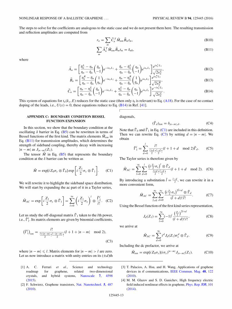
APPENDIX C: BOUNDARY CONDITION BESSELFUNCTION EXPANSION
In this section, we show that the boundary condition at theoscillating δ barrier in Eq. (B5) can be rewritten in terms ofBessel functions of the first kind. The matrix elements Mnm inEq. (B11) for transmission amplitudes, which determines thestrength of sideband coupling, thereby decay with increasing|n − m| as J|n−m|(Z1).
The tensor M in Eq. (B5) that represents the boundarycondition at the δ barrier can be written as
M = exp[iZ0σx ⊗ �0] exp
[iZ1
2σx ⊗ �1
]. (C1)
We will rewrite it to highlight the sideband space distribution.We will start by expanding the ac part of it in a Taylor series,
MAC = exp
[iZ1
2σx ⊗ �1
]=
∞∑l=0
(iZ1
2σx
)l
⊗ �l1
l!. (C2)
Let us study the off-diagonal matrix �1 taken to the lth power,i.e., �l
1. Its matrix elements are given by binomial coefficients,
(�l
1
)nm
= l!l+|n−m|
2 ! l−|n−m|2 !
(l + 1 + |n − m| mod 2),
(C3)
where |n − m| � l. Matrix elements for |n − m| > l are zero.Let us now introduce a matrix with unity entries on its (±d)th
diagonals,
(�d )nm = δ|n−m|,d . (C4)
Note that �0 and �1 in Eq. (C1) are included in this definition.Then we can rewrite Eq. (C3) by setting d = |n − m|. Weobtain
�l1 =
l∑d=0
l!l+d
2 ! l−d2 !
(l + 1 + d mod 2)�d . (C5)
The Taylor series is therefore given by
MAC =∞∑l=0
l∑d=0
(i Z1
2 σx
)l ⊗ �d
l+d2 ! l−d
2 !(l + 1 + d mod 2). (C6)
By introducing a substitution l = l−d2 , we can rewrite it in a
more convenient form,
MAC =∞∑l=0
∞∑d=0
(i Z1
2 σx
)2l+d ⊗ �d
(l + d)! l!. (C7)
Using the Bessel function of the first kind series representation,
Jd (Z1) =∞∑l=0
(−1)l(
Z12
)2l+d
(l + d)! l!, (C8)
we arrive at
MAC =∞∑
d=0
idJd (Z1)σdx ⊗ �d . (C9)
Including the dc prefactor, we arrive at
Mnm = exp[iZ0σx](iσx)|n−m|J|n−m|(Z1). (C10)
[1] A. C. Ferrari et al., Science and technologyroadmap for graphene, related two-dimensionalcrystals, and hybrid systems, Nanoscale 7, 4598(2015).
[2] F. Schwierz, Graphene transistors, Nat. Nanotechnol. 5, 487(2010).
[3] T. Palacios, A. Hsu, and H. Wang, Applications of graphenedevices in rf communications, IEEE Commun. Mag. 48, 122(2010).
[4] M. M. Glazov and S. D. Ganichev, High frequency electricfield induced nonlinear effects in graphene, Phys. Rep. 535, 101(2014).
125445-13

Y. KORNIYENKO, O. SHEVTSOV, AND T. LOFWANDER PHYSICAL REVIEW B 94, 125445 (2016)
[5] T. Otsuji, S. A. Boubanga Tombet, A. Satou, H. Fukidome,M. Suemitsu, E. Sano, V. Popov, M. Ryzhii, and V. Ryzhii,Graphene materials and devices in terahertz science and tech-nology, MRS Bull. 37, 1235 (2012).
[6] F. H. L. Koppens, T. Mueller, P. Avouris, A. C. Ferrari,M. S. Vitiello, and M. Polini, Photodetectors based on graphene,other two-dimensional materials and hybrid systems, Nat.Nanotechnol. 9, 780 (2014).
[7] R. Cheng, J. Bai, L. Liao, H. Zhou, Y. Chen, L. Liu, Y.-C. Lin,S. Jiang, Y. Huang, and X. Duan, High-frequency self-alignedgraphene transistors with transferred gate stacks, Proc. Natl.Acad. Sci. USA 109, 11588 (2012).
[8] H. Wang, D. Nezich, J. Kong, and T. Palacios, Graphenefrequency multipliers, IEEE Electron Device Lett. 30, 547(2009).
[9] O. Habibpour, S. Cherednichenko, J. Vukusic, K. Yhland, andJ. Stake, A subharmonic graphene FET mixer, IEEE ElectronDevice Lett. 33, 71 (2012).
[10] L. Vicarelli, M. S. Vitiello, D. Coquillat, A. Lombardo, A. C.Ferrari, W. Knap, M. Polini, V. Pellegrini, and A. Tredicucci,Graphene field-effect transistors as room-temperature terahertzdetectors, Nat. Mater. 11, 865 (2012).
[11] M. Mittendorff, S. Winnerl, J. Kamann, J. Eroms, D. Weiss, H.Schneider, and M. Helm, Ultrafast graphene-based broadbandTHz detector, Appl. Phys. Lett. 103, 021113 (2013).
[12] X. Cai, A. B. Sushkov, R. J. Suess, M. M. Jadidi, G. S. Jenkins,L. O. Nyakiti, R. L. Myers-Ward, S. Li, J. Yan, D. K. Gaskill,T. E. Murphy, H. D. Drew, and M. S. Fuhrer, Sensitive room-temperature terahertz detection via the photothermoelectriceffect in graphene, Nat. Nanotechnol. 9, 814 (2014).
[13] A. Zak, M. A. Andersson, M. Bauer, J. Matukas, A. Lisauskas,H. G. Roskos, and J. Stake, Antenna-integrated 0.6 THz FETdirect detectors based on CVD graphene, Nano Lett. 14, 5834(2014).
[14] P. Rickhaus, P. Makk, M.-H. Liu, E. Tovari, M. Weiss, R.Maurand, K. Richter, and C. Schonenberger, Snake trajectoriesin ultraclean graphene p–n junctions, Nat. Commun. 6, 1 (2015).
[15] S. Chen, Z. Han, M. M. Elahi, K. M. M. Habib, L. Wang, B. Wen,Y. Gao, T. Taniguchi, K. Watanabe, J. Hone, A. W. Ghosh, andC. R. Dean, Electron optics with ballistic graphene junctions,arXiv:1602.08182v1.
[16] Y. Zhao, J. Wyrick, F. D. Natterer, J. F. Rodriguez-Nieva, C.Lewandowski, K. Watanabe, T. Taniguchi, L. S. Levitov, N.B. Zhitenev, and J. A. Stroscio, Creating and probing electronwhispering-gallery modes in graphene, Science (NY) 348, 672(2015).
[17] D. A. Bandurin, I. Torre, R. K. Kumar, M. Ben Shalom,A. Tomadin, A. Principi, G. H. Auton, E. Khestanova,K. S. Novoselov, I. V. Grigorieva, L. A. Ponomarenko,A. K. Geim, and M. Polini, Negative local resistance caused byviscous electron backflow in graphene, Science (NY) 351, 1055(2016).
[18] J. Crossno, J. K. Shi, K. Wang, X. Liu, A. Harzheim, A. Lucas,S. Sachdev, P. Kim, T. Taniguchi, K. Watanabe, T. A. Ohki, andK. C. Fong, Observation of the Dirac fluid and the breakdownof the Wiedemann-Franz law in graphene, Science (NY) 351,1058 (2016).
[19] F. Ghahari, H.-Y. Xie, T. Taniguchi, K. Watanabe, M. S. Foster,and P. Kim, Enhanced Thermoelectric Power in Graphene:
Violation of the Mott Relation by Inelastic Scattering, Phys.Rev. Lett. 116, 136802 (2016).
[20] E. Prada, P. San-Jose, and H. Schomerus, Quantum pumping ingraphene, Phys. Rev. B 80, 245414 (2009).
[21] L. E. F. Foa Torres, H. L. Calvo, C. G. Rocha, and G.Cuniberti, Enhancing single-parameter quantum charge pump-ing in carbon-based devices, Appl. Phys. Lett. 99, 092102(2011).
[22] P. San-Jose, E. Prada, S. Kohler, and H. Schomerus, Single-parameter pumping in graphene, Phys. Rev. B 84, 155408(2011).
[23] P. San-Jose, E. Prada, H. Schomerus, and S. Kohler, Laser-induced quantum pumping in graphene, Appl. Phys. Lett. 101,153506 (2012).
[24] S. A. Mikhailov and K. Ziegler, New Electromagnetic Mode inGraphene, Phys. Rev. Lett. 99, 016803 (2007).
[25] S. A. Mikhailov and K. Ziegler, Nonlinear electromagneticresponse of graphene: frequency multiplication and the self-consistent-field effects, J. Phys.: Condens. Matter 20, 384204(2008).
[26] S. V. Syzranov, M. V. Fistul, and K. B. Efetov, Effect of radiationon transport in graphene, Phys. Rev. B 78, 045407 (2008).
[27] K. L. Ishikawa, Nonlinear optical response of graphene in timedomain, Phys. Rev. B 82, 201402(R) (2010).
[28] H. L. Calvo, P. M. Perez-Piskunow, S. Roche, and L. E. F.Foa Torres, Laser-induced effects on the electronic featuresof graphene nanoribbons, Appl. Phys. Lett. 101, 253506(2012).
[29] I. Al-Naib, J. E. Sipe, and M. M. Dignam, High harmonic gen-eration in undoped graphene: Interplay of inter- and intrabanddynamics, Phys. Rev. B 90, 245423 (2014).
[30] C. Sinha and R. Biswas, Transmission of electron throughmonolayer graphene laser barrier, Appl. Phys. Lett. 100, 183107(2012).
[31] S. A. Jafari, Nonlinear optical response in gapped graphene,J. Phys.: Condens. Matter 24, 205802 (2012).
[32] H. K. Avetissian, A. K. Avetissian, G. F. Mkrtchian, andK. V. Sedrakian, Multiphoton resonant excitation of Fermi-Diracsea in graphene at the interaction with strong laser fields,J. Nanophoton. 6, 061702 (2012).
[33] H. K. Avetissian, G. F. Mkrtchian, K. G. Batrakov, S. A.Maksimenko, and A. Hoffmann, Multiphoton resonant excita-tions and high-harmonic generation in bilayer graphene, Phys.Rev. B 88, 165411 (2013).
[34] B. Trauzettel, Y. M. Blanter, and A. F. Morpurgo, Photon-assisted electron transport in graphene: Scattering theory anal-ysis, Phys. Rev. B 75, 035305 (2007).
[35] M. A. Zeb, K. Sabeeh, and M. Tahir, Chiral tunneling througha time-periodic potential in monolayer graphene, Phys. Rev. B78, 165420 (2008).
[36] C. G. Rocha, Luis E. F. Foa Torres, and G. Cuniberti, ac transportin graphene-based Fabry-Perot devices, Phys. Rev. B 81, 115435(2010).
[37] S. E. Savel’ev, W. Hausler, and P. Hanggi, Current Resonancesin Graphene with Time-Dependent Potential Barriers, Phys. Rev.Lett. 109, 226602 (2012).
[38] W.-T. Lu, S.-J. Wang, W. Li, Y.-L. Wang, C.-Z. Ye, and H.Jiang, Fano-type resonance through a time-periodic potential ingraphene, J. Appl. Phys. 111, 103717 (2012).
125445-14

NONLINEAR RESPONSE OF A BALLISTIC GRAPHENE . . . PHYSICAL REVIEW B 94, 125445 (2016)
[39] L. Z. Szabo, M. G. Benedict, A. Czirjak, and P. Foldi, Relativisticelectron transport through an oscillating barrier: Wave-packetgeneration and Fano-type resonances, Phys. Rev. B 88, 075438(2013).
[40] R. Zhu, J.-H. Dai, and Y. Guo, Fano resonance in the nonadia-batically pumped shot noise of a time-dependent quantum wellin a two-dimensional electron gas and graphene, J. Appl. Phys.117, 164306 (2015).
[41] Y. Korniyenko, O. Shevtsov, and T. Lofwander, Resonantsecond-harmonic generation in a ballistic graphene transistorwith an ac-driven gate, Phys. Rev. B 93, 035435 (2016).
[42] P. F. Bagwell and R. K. Lake, Resonances in transmissionthrough an oscillating barrier, Phys. Rev. B 46, 15329 (1992).
[43] M. H. Pedersen and M. Buttiker, Scattering theory of photon-assisted electron transport, Phys. Rev. B 58, 12993 (1998).
[44] G. Platero and R. Aguado, Photon-assisted transport in semi-conductor nanostructures, Phys. Rep. 395, 1 (2004).
[45] S. Kohler, J. Lehmann, and P. Hanggi, Driven quantum transporton the nanoscale, Phys. Rep. 406, 379 (2005).
[46] B. Huard, N. Stander, J. A. Sulpizio, and D. Goldhaber-Gordon,Evidence of the role of contacts on the observed electron-holeasymmetry in graphene, Phys. Rev. B 78, 121402 (2008).
[47] We note that for a system translationally invariant in thetransverse direction, one has to compute conductance per unitlength. In our previous work (cf. Eqs. (D10)–(E2) in Ref. [41]),
we missed the 1/2π prefactor associated with ky integration inthe current and conductance formulas, which we include here[see Eq. (7)]. The main results of Ref. [41] are not affected,although the scales in Figs. 3(b) and 4 should include thisprefactor.
[48] J. Tworzydło, B. Trauzettel, M. Titov, A. Rycerz, and C. W. J.Beenakker, Sub-Poissonian Shot Noise in Graphene, Phys. Rev.Lett. 96, 246802 (2006).
[49] B. Ricco and M. Y. Azbel, Physics of resonant tunneling. Theone-dimensional double-barrier case, Phys. Rev. B 29, 1970(1984).
[50] H. Yamamoto, Resonant tunneling condition and transmis-sion coefficient in a symmetrical one-dimensional rectangulardouble-barrier system, Appl. Phys. A 42, 245 (1987).
[51] R. Danneau, F. Wu, M. F. Craciun, S. Russo, M. Y. Tomi,J. Salmilehto, A. F. Morpurgo, and P. J. Hakonen, ShotNoise in Ballistic Graphene, Phys. Rev. Lett. 100, 196802(2008).
[52] G. Giovannetti, P. A. Khomyakov, G. Brocks, V. M. Karpan, J.Van Den Brink, and P. J. Kelly, Doping Graphene with MetalContacts, Phys. Rev. Lett. 101, 026803 (2008).
[53] A. Laitinen, G. S. Paraoanu, M. Oksanen, M. F. Craciun,S. Russo, E. Sonin, and P. Hakonen, Contact doping, Kleintunneling, and asymmetry of shot noise in suspended graphene,Phys. Rev. B 93, 115413 (2016).
125445-15