Nonisolated DC-DC Converters with Wide Conversion Range ...
11
2168-6777 (c) 2018 IEEE. Personal use is permitted, but republication/redistribution requires IEEE permission. See http://www.ieee.org/publications_standards/publications/rights/index.html for more information. This article has been accepted for publication in a future issue of this journal, but has not been fully edited. Content may change prior to final publication. Citation information: DOI 10.1109/JESTPE.2019.2892977, IEEE Journal of Emerging and Selected Topics in Power Electronics George Harrison de Alcântara Bastos, Levy Ferreira Costa, Fernando Lessa Tofoli, Grover Victor Torrico Bascopé, and René Pastor Torrico Bascopé * *Corresponding author AbstractThis paper presents the conception of a family of dc-dc converters with wide conversion range (WCR) based on the multi-state switching cell (MSSC) for high-power, high-current applications. The resulting topologies allow achieving high-voltage step-up/step-down in a modular approach, as the WCR-MSSC cell is obtained by using isolated secondary windings coupled to the autotransformer of the MSSC with series-connected controlled rectifiers. Depending on the transformer turns ratio, it is possible to adjust the static gain and reduce the voltage stresses across the main switches, thus allowing the use of metal oxide semiconductor field effect transistors (MOSFETs) with low on-resistance R DS(on) , as efficiency is improved as a consequence of minimized conduction losses. A dc-dc boost- type converter based on the four-state switching cell (4SSC) is also implemented, thoroughly analyzed, and evaluated experimentally to demonstrate the advantages associated to the proposed approach in the conception of novel dc-dc converter topologies for this purpose. Index Terms—dc-dc converters, multi-state switching cell, step-up dc-dc converters, wide conversion range. I. INTRODUCTION Dc-dc converters play an important role in modern applications when adapting existing voltage and current levels involving distinct types of sources and loads. Renewable energy systems, e.g., solar photovoltaic, fuel cell, and small wind energy conversion ones may depend on low dc voltages (12 Vdc – 48 Vdc) due to the presence of a dc- link composed by filter capacitors or back-up batteries. In practice, many series-connected elements are often undesirable to avoid redundancy, minimize cost, and increase robustness. Low dc voltages are then supposed to be stepped up to levels ranging from 200 Vdc to 800 Vdc to supply cascaded single-phase or three-phase voltage source inverters typically found in off-grid and on-grid systems, submerged water pumps, motor drives, among others [1] [2]. In applications involving wide conversion range (WCR), power converters employing high-frequency transformers are the most obvious choice since the static gain can be adjusted not only according to the duty cycle, but also the turns ratio between the windings. However, it is worth to mention that the transformer leads to the increase of overall size, weight, and volume of the converter in high-power applications [3]. If galvanic isolation is not necessary, it is possible to use nonisolated dc-dc converters instead with consequent reduction of dimensions and increase of efficiency due to the lack of a high-frequency transformer. The classical buck and boost converters are the preliminary choices in voltage step- down and step-up, respectively, mainly due to simplicity, low component count, and reduced stresses if compared with the buck-boost, Ćuk, SEPIC, and Zeta topologies, although some important practical issues must be taken into account. In order to achieve WCR with the aforementioned topologies, extremely low or high duty ratios would be necessary, thus demanding the use of high-cost and complex drivers for this purpose. When using boost-derived converters and high duty ratios, the parasitic resistance regarding the filter inductor also causes appreciable I 2 R losses, thus leading to poor efficiency and reduction of the static gain [4]. Literature presents some interesting approaches that allow obtaining WCR in both step-down and step-up nonisolated dc-dc converters. Considering particular advantages and disadvantages addressed to the existing structures, cascaded converters, coupled-inductor-based converters, switched- capacitor-based converters, and converters using voltage multiplier cells (VMCs) can be used in practice. Perhaps one of the earliest works on the subject is the one introduced in [5], where single-switch topological variations of cascaded dc-dc converters are described. The so-called quadratic converters provide high-voltage step-up or step- down by simply assuming that the overall static gain is equal to the product of the static gains associated to the existing converters. Even though this is a modular solution able to achieve WCR in both cases, the resulting topologies are not viable for high-power applications because energy is processed by multiple cascaded stages, thus compromising the overall efficiency. The appreciable voltage stresses regarding the semiconductor elements are also of major concern. Coupled inductors are a possible alternative to extend the static gain of dc-dc converters [6]. The leakage inductance can be used to limit the diode current falling rate, thus minimizing the diode reverse-recovery problem. Furthermore, the coupled inductor is employed as a transformer to avoid operation with very high duty ratios and reduce the current ripple in high step-up conversion [7]. For instance, a coupled-inductor-based dc-dc boost converter with low component count is introduced in [8], where the turns ratio allows adjusting the static gain as desired in a simple and straightforward approach. However, the leakage inductance may lead to high voltage spikes, which will increase the voltage stress across the switch causing high electromagnetic interference (EMI) levels and reducing efficiency. The input current is also pulsating, as a low-pass filter may be necessary to further mitigate EMI issues. Capacitors can be integrated to dc-dc converters by using a switched approach that allows increasing the voltage gain. An example is given in [9], where high-voltage step-up can be achieved by properly increasing the number of capacitors. Since the converter operates typically with low duty cycle, the reverse recovery issue of the output diode is alleviated. The capacitors behave as series-connected voltage sources as the current flows through all of them. Their respective equivalent series resistances must be properly minimized by the parallel association of individual components to achieve a Nonisolated DC-DC Converters with Wide Conversion Range for High-Power Applications
Transcript of Nonisolated DC-DC Converters with Wide Conversion Range ...
2168-6777 (c) 2018 IEEE. Personal use is permitted, but republication/redistribution requires IEEE permission. See http://www.ieee.org/publications_standards/publications/rights/index.html for more information.
This article has been accepted for publication in a future issue of this journal, but has not been fully edited. Content may change prior to final publication. Citation information: DOI 10.1109/JESTPE.2019.2892977, IEEEJournal of Emerging and Selected Topics in Power Electronics
George Harrison de Alcântara Bastos, Levy Ferreira Costa, Fernando Lessa Tofoli, Grover Victor Torrico Bascopé, and René Pastor Torrico Bascopé*
*Corresponding author
AbstractThis paper presents the conception of a family of dc-dc converters with wide conversion range (WCR) based on the multi-state switching cell (MSSC) for high-power, high-current applications. The resulting topologies allow achieving high-voltage step-up/step-down in a modular approach, as the WCR-MSSC cell is obtained by using isolated secondary windings coupled to the autotransformer of the MSSC with series-connected controlled rectifiers. Depending on the transformer turns ratio, it is possible to adjust the static gain and reduce the voltage stresses across the main switches, thus allowing the use of metal oxide semiconductor field effect transistors (MOSFETs) with low on-resistance RDS(on), as efficiency is improved as a consequence of minimized conduction losses. A dc-dc boost-type converter based on the four-state switching cell (4SSC) is also implemented, thoroughly analyzed, and evaluated experimentally to demonstrate the advantages associated to the proposed approach in the conception of novel dc-dc converter topologies for this purpose. Index Terms—dc-dc converters, multi-state switching cell, step-up dc-dc converters, wide conversion range.
I. INTRODUCTION
Dc-dc converters play an important role in modern applications when adapting existing voltage and current levels involving distinct types of sources and loads. Renewable energy systems, e.g., solar photovoltaic, fuel cell, and small wind energy conversion ones may depend on low dc voltages (12 Vdc – 48 Vdc) due to the presence of a dc-link composed by filter capacitors or back-up batteries. In practice, many series-connected elements are often undesirable to avoid redundancy, minimize cost, and increase robustness. Low dc voltages are then supposed to be stepped up to levels ranging from 200 Vdc to 800 Vdc to supply cascaded single-phase or three-phase voltage source inverters typically found in off-grid and on-grid systems, submerged water pumps, motor drives, among others [1] [2].
In applications involving wide conversion range (WCR), power converters employing high-frequency transformers are the most obvious choice since the static gain can be adjusted not only according to the duty cycle, but also the turns ratio between the windings. However, it is worth to mention that the transformer leads to the increase of overall size, weight, and volume of the converter in high-power applications [3].
If galvanic isolation is not necessary, it is possible to use nonisolated dc-dc converters instead with consequent reduction of dimensions and increase of efficiency due to the lack of a high-frequency transformer. The classical buck and boost converters are the preliminary choices in voltage step-down and step-up, respectively, mainly due to simplicity, low component count, and reduced stresses if compared with the buck-boost, Ćuk, SEPIC, and Zeta topologies, although some important practical issues must be taken into account. In
order to achieve WCR with the aforementioned topologies, extremely low or high duty ratios would be necessary, thus demanding the use of high-cost and complex drivers for this purpose. When using boost-derived converters and high duty ratios, the parasitic resistance regarding the filter inductor also causes appreciable I2R losses, thus leading to poor efficiency and reduction of the static gain [4].
Literature presents some interesting approaches that allow obtaining WCR in both step-down and step-up nonisolated dc-dc converters. Considering particular advantages and disadvantages addressed to the existing structures, cascaded converters, coupled-inductor-based converters, switched-capacitor-based converters, and converters using voltage multiplier cells (VMCs) can be used in practice.
Perhaps one of the earliest works on the subject is the one introduced in [5], where single-switch topological variations of cascaded dc-dc converters are described. The so-called quadratic converters provide high-voltage step-up or step-down by simply assuming that the overall static gain is equal to the product of the static gains associated to the existing converters. Even though this is a modular solution able to achieve WCR in both cases, the resulting topologies are not viable for high-power applications because energy is processed by multiple cascaded stages, thus compromising the overall efficiency. The appreciable voltage stresses regarding the semiconductor elements are also of major concern.
Coupled inductors are a possible alternative to extend the static gain of dc-dc converters [6]. The leakage inductance can be used to limit the diode current falling rate, thus minimizing the diode reverse-recovery problem. Furthermore, the coupled inductor is employed as a transformer to avoid operation with very high duty ratios and reduce the current ripple in high step-up conversion [7]. For instance, a coupled-inductor-based dc-dc boost converter with low component count is introduced in [8], where the turns ratio allows adjusting the static gain as desired in a simple and straightforward approach. However, the leakage inductance may lead to high voltage spikes, which will increase the voltage stress across the switch causing high electromagnetic interference (EMI) levels and reducing efficiency. The input current is also pulsating, as a low-pass filter may be necessary to further mitigate EMI issues.
Capacitors can be integrated to dc-dc converters by using a switched approach that allows increasing the voltage gain. An example is given in [9], where high-voltage step-up can be achieved by properly increasing the number of capacitors. Since the converter operates typically with low duty cycle, the reverse recovery issue of the output diode is alleviated. The capacitors behave as series-connected voltage sources as the current flows through all of them. Their respective equivalent series resistances must be properly minimized by the parallel association of individual components to achieve a
Nonisolated DC-DC Converters with Wide Conversion Range
for High-Power Applications

2168-6777 (c) 2018 IEEE. Personal use is permitted, but republication/redistribution requires IEEE permission. See http://www.ieee.org/publications_standards/publications/rights/index.html for more information.
This article has been accepted for publication in a future issue of this journal, but has not been fully edited. Content may change prior to final publication. Citation information: DOI 10.1109/JESTPE.2019.2892977, IEEEJournal of Emerging and Selected Topics in Power Electronics
given capacitance since they can compromise efficiency. Drive circuitry also becomes more complex as more switches are added, which are not connected to the same reference node. It is also worth to mention that the voltage stresses across them are not the same, leading to the specification of active switches with multiple ratings.
VMCs have been successfully used to obtain novel converter topologies with WCR [10]. A modular and flexible approach results when combining diodes and capacitors as in [11], where a family of nonisolated dc-dc converters is proposed. However, as more VMCs are added, high component count associated to increased conduction and switching losses in the multiplier diodes are possible drawbacks.
Even though there are many other dc-dc converter topologies with high-voltage step-up characteristic, most solutions are only able to process power levels lower than 1 kW, thus motivating the search for topologies able to achieve higher power levels with increased efficiency in [12]. When dealing with high-power, high-current applications, interleaving is one of the most popular and obvious choices as a modular approach, where the output power can be increased by using additional switches, inductors, and diodes. Literature presents some dc-dc interleaved boost converters capable of achieving high-voltage step-up based on VMCs [13], coupled inductors [14], or a combination of both approaches [15]. For instance, a six-phase interleaved double dual boost converter is proposed in [16], whose efficiency is 92.8% at the rated power of 2.2 kW. However, the voltages across the output filter capacitors must be balanced and controlled independently using a proper control scheme. Another important issue that must be taken into account in interleaving topologies lies in the fact that current sharing among the phases can be compromised due to eventual inherent differences regarding the semiconductor elements and inductors, while duty cycle mismatch must also be analyzed in detail [17]. Consequently, balancing the current through the phases may require the use of complex control techniques as described in [18].
Within this context, this work proposes a family of dc-dc converters with WCR adequate for high-power, high-current applications. It consists in a modular approach that allows modifying the static gain while also keeping reduced voltage stresses across the semiconductors, which is essential to minimize conduction losses and achieve high efficiency at high power levels. Thus it is possible to derive unidirectional or bidirectional step-down, step-up, and step-up/step-down dc-dc converter topologies that can be used in a wide range of applications. Since renewable energy conversion systems often require dc-dc converters with high-voltage step-up, a boost-type converter is proposed and thoroughly evaluated so that it is possible to validate the theoretical assumptions. A 3-kW experimental prototype is developed, where it is possible to validate the theoretical assumptions.
II. GENERATION OF NOVEL CONVERTER TOPOLOGIES AND
PROPOSED HIGH-VOLTAGE STEP-UP BOOST CONVERTER
The canonical cell or two-state switching cell (2SSC) is part of the basic dc-dc converter topologies, being composed by one active switch and one diode that operate complementarily [19, 20]. This arrangement can also be represented using the pulse width modulation (PWM) switch model for the small-signal analysis in terms of a three-terminal element [21, 22]. Bidirectional converters can also
be obtained if the diode is simply replaced by an active switch.
The load power in the aforementioned topologies is processed by a single semiconductor in each operating stage, as such structures present inherent limitation when power levels come to increase. The 2SSC can then be replaced by the multi-state switching cell (MSSC), which is composed by several 2SSCs connected to each other by an autotransformer to achieve higher current levels, as the number of switching states can be increased as associated to additional semiconductors [23]. A bidirectional version of the MSSC is shown in Fig. 1 (a), which employs one autotransformer with multiple windings connected to the legs composed by lower-side active switches S1, S2,, Sn and upper-side active switches S1’, S2’,,Sn’. It is also worth to mention that a unidirectional version can be obtained by replacing the upper-side active switches for diodes. The autotransformer in this case plays a key role in providing good current sharing among the several legs constituted by semiconductors considering that all windings have the same number of turns.
Depending on the number of switching states N assumed by the MSSC, there are N-1 possible operating regions, while the gating signals that drive the active switches must be phase-shifted by 360/(N-1) analogously to interleaving. However, if the autotransformer presents unity turns ratio, it is possible to achieve high power levels in a modular approach with good current sharing without the need of special control schemes. Other prominent advantages addressed to the MSSC are reduced current stresses through semiconductors, with minimized conduction losses when metal oxide semiconductor field effect transistors (MOSFETs) are employed; consequent increase of overall efficiency; improved utilization of heat sinks with proper distribution of losses; reduced dimensions and weight of filter elements, which are designed for a multiple of the switching frequency.
If the 2SSC that exists in the six classical dc-dc converters is simply replaced by the bidirectional version of the MSSC shown in Fig. 1 (a), the very same static gain is obtained considering the operation in continuous conduction mode (CCM). In order to obtain dc-dc converters with WCR, several additional secondary windings can be coupled to the windings of the autotransformer of the MSSC and associated to series-connected active rectifiers as seen in Fig. 1 (b), as the resulting arrangement is called WCR-MSSC. It is able to provide unidirectional or bidirectional power flow, also allowing the increase of power levels and/or the conversion ratio as desired. It is also worth to mention that the autotransformer becomes a multi-phase transformer since the secondary windings are coupled to the primary ones, which formerly belong to the MSSC.
The canonical cell is a three-port element that exists in the classical dc-dc converters, been represented by terminals a, b, and c in the conventional buck, boost, buck-boost, Ćuk, single-ended primary inductance converter (SEPIC), and Zeta topologies in Fig. 2. Although only their respective bidirectional versions are shown in a more generic representation, it can be stated that unidirectional converters can be promptly obtained when substituting switch S1’ for a diode. This switching cell can then be simply replaced by the proposed WCR-MSSC shown in Fig. 1 (b), resulting in a family of bidirectional converters for high-voltage step-up and/or step-down as shown in Fig. 2. The lower-side active switches S1, S2,, Sn and upper-side active switches S1’, S2’,,Sn’ are part of the MSSC. On the other hand, Sajn and

2168-6777 (c) 2018 IEEE. Personal use is permitted, but republication/redistribution requires IEEE permission. See http://www.ieee.org/publications_standards/publications/rights/index.html for more information.
This article has been accepted for publication in a future issue of this journal, but has not been fully edited. Content may change prior to final publication. Citation information: DOI 10.1109/JESTPE.2019.2892977, IEEEJournal of Emerging and Selected Topics in Power Electronics
Sajn’ denote active switches that are part of a given controlled rectifier bridge j, being n the total number of phases of the transformer. Besides, unidirectional converters can be obtained substituting S1’, S2’,, Sn’, Sajn, and Sajn’ for diodes.
The so-called WCR-MSSC dc-dc converters can be employed in distinct high-power applications, e.g., solar photovoltaic systems [24]. The following advantages can then be addressed to the resulting structures: reduced current stresses regarding the semiconductor elements, since the total current is shared among several legs; reduced voltage stresses across the active switches if compared with the conventional dc-dc converters; inherent modularity; possibility to achieve unidirectional or bidirectional power flow; distinct configurations such as wye or polygon connection can be employed in the secondary side of the multi-phase transformer.
Considering that nonisolated dc-dc converters for high-voltage step-up applications are a modern trend in power electronics, the unidirectional boost converter employing the four-state switching cell (4SSC) shown in
Fig. 3 is presented and analyzed in detail to demonstrate the claimed advantages. It is composed by an input voltage source VIN; a filter inductor L1; a three-phase Y-Y (wye-wye) transformer with turns ratio n=Ns/Np; active switches S1, S2, and S3; rectifier diodes D1D9; auxiliary clamping capacitors
C1 and C2; an output filter capacitor Co; and a load resistor Ro.
(a) (b)
Fig. 1. (a) Bidirectional versions of the (a) MSSC; (b) WCR-MSSC cell.
c
b
a
c
b
a
S1
S1'
C1
C2
Co
NP1
NPn S1 S2 Sn
S1' S2' Sn'
Sa11 Sa12 Sa1n
Sa11' Sa12' Sa1n'
Vo
Ro
VIN
L1 L1
VIN
Co Ro
Vo
NS1
NSn
(a) (b)
(c) (d)
(e) (f)
Fig. 2. Classical and WCR-MSSC bidirectional dc-dc converters; (a) buck, (b) boost, (c) buck-boost, (d) Ćuk, (e) SEPIC, and (f) Zeta topologies.

2168-6777 (c) 2018 IEEE. Personal use is permitted, but republication/redistribution requires IEEE permission. See http://www.ieee.org/publications_standards/publications/rights/index.html for more information.
This article has been accepted for publication in a future issue of this journal, but has not been fully edited. Content may change prior to final publication. Citation information: DOI 10.1109/JESTPE.2019.2892977, IEEEJournal of Emerging and Selected Topics in Power Electronics
Since the 4SSC is used in this case, the gating signals of switches S1, S2, and S3 must be phase-shifted by [360/(4-1)]=120. Besides, three operating regions exist: R1 (0<D<1/3), where a single active switch is on in a given operating stage; R2 (1/3<D<2/3), where up to two active switches are on simultaneously in a given operating stage; and R3 (2/3<D<1), where up to three active switches are on simultaneously in a given operating stage. It is worth to mention that a same converter presents distinct operating stages for each one of them considering the switching states shown in Table I, thus leading to particularly different qualitative and quantitative analyses.
Applying the volt-second balance to the boost converter operating in CCM for each one of the aforementioned regions, the static gain plots in
Fig. 4 can be obtained. It can be seen that it is not possible to achieve high-voltage step-up in region R1 since the voltage induced in the secondary windings is somewhat low, unless if high turns ratio is adopted. On the other hand, region R3 provides WCR, although extreme duty ratios should be avoided in practice to avoid appreciable I2R loss due to parasitic resistance of the filter inductor [25]. This is the main reason why the analysis carried out in this work is restricted to region R2 so that it is possible to develop an experimental prototype.
TABLE I SWITCHING STATES OF THE PROPOSED 4SSC-BASED BOOST CONVERTER IN
CCM
Operating Stage Switching States (S1, S2, S3)
R1 R2 R3 1 ON, OFF, OFF OFF, ON, ON ON, ON, ON 2 OFF, OFF, OFF OFF, OFF, ON OFF, ON, ON 3 OFF, ON, OFF ON, OFF, ON ON, ON, ON 4 OFF, OFF, OFF ON, OFF, OFF ON, OFF, ON 5 OFF, OFF, ON ON, ON, OFF ON, ON, ON 6 OFF, OFF, OFF OFF, ON, OFF ON, ON, OFF
S1
D1 D2 D3
D4 D5 D6
D7 D8 D9
C1
RCO
iSNpVIN
Ns
V
DC Link
Three-Phase Transformer
MSSC
S2 S3
Three-Phase Rectifier
L1
C2
O
O
Fig. 3. High-voltage step-up dc-dc boost converter based on the WCR-4SSC.
Fig. 4. Static gain of the 4SSC-based boost converter in CCM for distinct turns ratio as a function of the duty cycle.
III. QUALITATIVE ANALYSIS
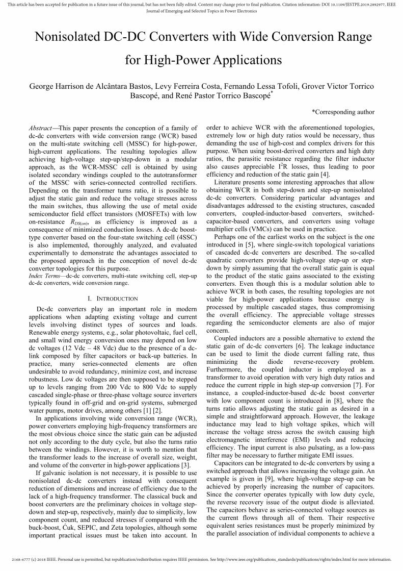
Considering that the converter operates in region R2 (1/3<D<2/3) under CCM and steady-state conditions, six stages result during one switching period Ts as shown in Fig. 5, while the theoretical waveforms are represented in Fig. 6. First stage [t0, t1] (Fig. 5 (a)): Switch S3 is turned on, while switches S1 and S2 keep their previous states and remain off and on, respectively. The current through L1 increases linearly, flowing through winding Tp2 and S2, and also through winding Tp3 and S3, as good current sharing is maintained considering that the number of turns is the same for all primary windings. Besides, part of the energy through Tp1 is directly transferred from the input source to the load. Diodes D2, D3, D4, D8, and D9 are reverse biased, while diodes D1, D5, D6, and D7 are forward biased. This stage finishes when S2 is turned off.
The voltage across L1 is given by:
11
3C
L IN
VV V
(1) where VC1 is the average voltage across capacitor C1.
The time interval that defines this stage is:
0 1
3 1
3sD T
t t
(2)
Second stage [t1, t2] (Fig. 5 (b)): Switch S2 is turned off, while switches S1 and S3 keep their previous states and remain off and on, respectively. The energy stored in L1 is transferred to C1 and C2 and the load, as the inductor current decreases linearly flowing through the primary windings. The inductor voltage polarity is reversed so that the magnetic flux is constant, as the voltages across S2 and C1 are equal. Besides, diodes D3, D4, D5, and D9 remain reverse biased, while D1, D2, D6, D7, and D8 are forward biased.
The voltage across L1 is given by:
11
2
3C
L IN
VV V (3)
The time interval that defines this stage is:
1 2
2 3
3sD T
t t
(4)
Third stage [t2, t3] (Fig. 5 (c)): Due to the inherent symmetry, this stage is analogous to the first one, although switch S1 is turned on instead, while switches S2 and S3 keep their previous states and remain off and on, respectively. Diodes D1, D3, D5, D7, and D9 are reverse biased, while diodes D2, D4, D6, and D8 are forward biased. Fourth stage [t3, t4] (Fig. 5 (d)): This stage is similar to the second one, but switch S3 is turned off and only S1 remains on. The energy stored in L1 is delivered to the load, auxiliary capacitors C1 and C2, and output filter capacitor Co. Diodes D2, D3, D4, D8, and D9 are forward biased due to the polarity of the voltage across the transformer windings. Fifth stage [t4, t5] (Fig. 5 (e)): This stage is analogous to the first and third ones, but switch S2 is turned on, while switches S1 and S3 keep their previous states and remain on and off, respectively. The current through L1 increases linearly. Diodes D1, D2, D6, D7, and D8 are reverse biased. Sixth stage [t5, t6] (Fig. 5 (f)): Switch S1 is turned off, while switches S2 and S3 keep their previous states and remain on and off, respectively. Diodes D1, D3, D5, D7, and D9 are forward biased due to the polarity of the voltage across the secondary windings. Inductor L1 provides energy to the load and capacitors C1, C2, and Co. This stage finishes when S3 is turned on once again as another switching cycle begins.
2168-6777 (c) 2018 IEEE. Personal use is permitted, but republication/redistribution requires IEEE permission. See http://www.ieee.org/publications_standards/publications/rights/index.html for more information.
This article has been accepted for publication in a future issue of this journal, but has not been fully edited. Content may change prior to final publication. Citation information: DOI 10.1109/JESTPE.2019.2892977, IEEEJournal of Emerging and Selected Topics in Power Electronics
(a) First stage (b) Second stage
(c) Third stage (d) Fourth stage
(e) Fifth stage (f) Sixth stage Fig. 5. Operating stages of the proposed dc-dc converter.
2168-6777 (c) 2018 IEEE. Personal use is permitted, but republication/redistribution requires IEEE permission. See http://www.ieee.org/publications_standards/publications/rights/index.html for more information.
This article has been accepted for publication in a future issue of this journal, but has not been fully edited. Content may change prior to final publication. Citation information: DOI 10.1109/JESTPE.2019.2892977, IEEEJournal of Emerging and Selected Topics in Power Electronics
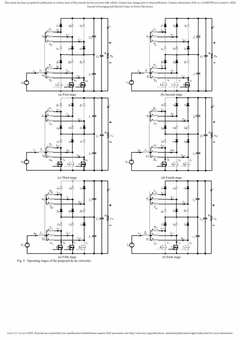
Fig. 6. Main theoretical waveforms.
IV. QUANTITATIVE ANALYSIS
A. Static Gain
From the analysis of the equivalent circuits and theoretical waveforms that describe the converter operation in CCM and region R2 as shown in Fig. 5 and Fig. 6, respectively, applying the volt-second balance to filter inductor L1 gives the static gain as:
1
, if 1 3 2 3 1IN
oV nG D
V D
(5)
The average voltages across capacitors C1 and C2 can be also be determined as:
1
, if 1 3 2 3
1-IN
C
VV D
D (6)
2
, if 1 3 2 3
1IN
C
n VV D
D
(7)
If a similar analysis is performed for regions R1 and R3, their respective static gains can be determined as in (8) and (9).
(1
1, if 0 1 3
1 3 )o
IN
V nG D
V D n D
(8)
1
, if 2 3 1 1IN
oV nG D
V D
(9)
If n=0 in (5), (8), and (9), the static gain is the same as that regarding the classical dc-dc boost converter, which is not able to provide high-voltage step-up in practice. However, the proposed topology allows achieving WCR as the number of turns involving the three-phase transformer increases.
B. Filter Inductor
The average and rms currents through the filter inductor are equal to the input current IIN, i.e.:
1 1
1
1oo
INL avg L rmsIN
I nPI I I
V D
(10)
where is the expected theoretical efficiency of the dc-dc converter, Po is the output power, and Io is the average output current.
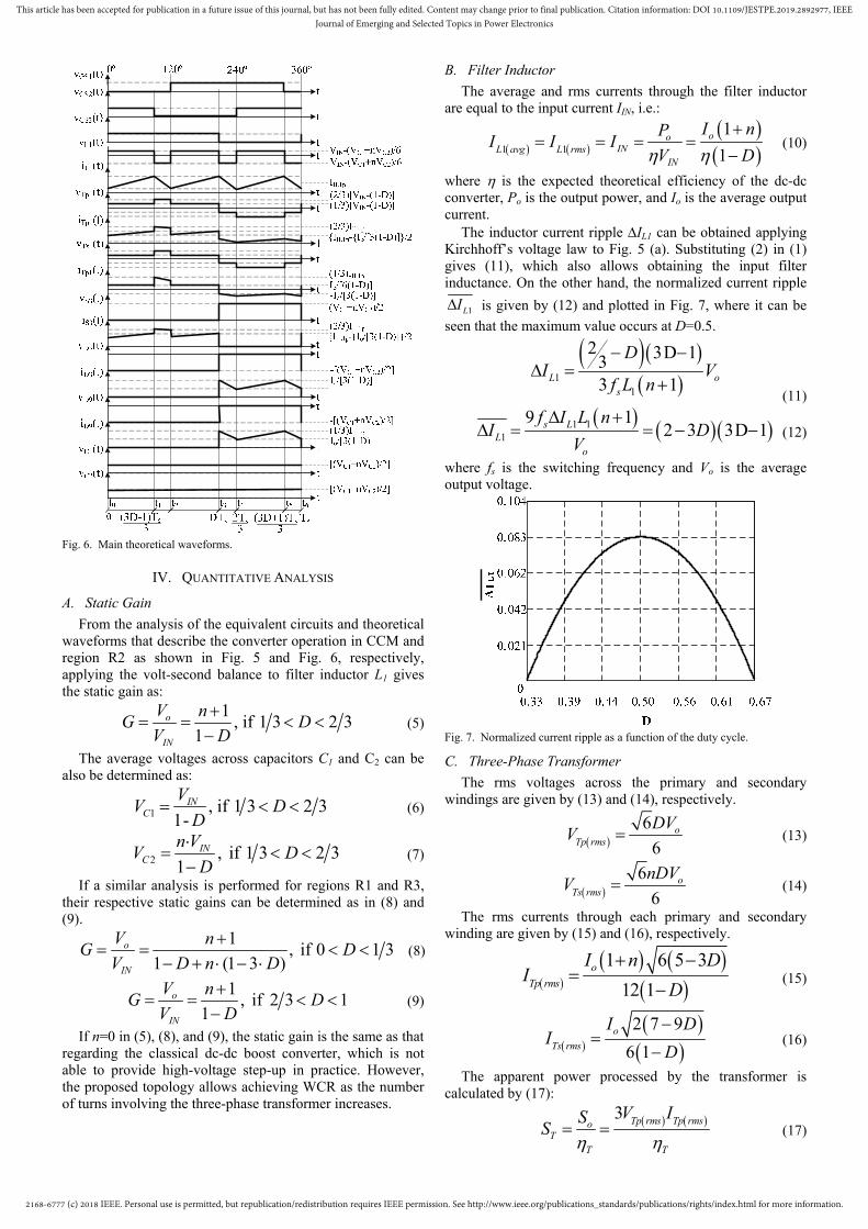
The inductor current ripple IL1 can be obtained applying Kirchhoff’s voltage law to Fig. 5 (a). Substituting (2) in (1) gives (11), which also allows obtaining the input filter inductance. On the other hand, the normalized current ripple
1LI is given by (12) and plotted in Fig. 7, where it can be
seen that the maximum value occurs at D=0.5.
1
1
2 3D 133 1L o
s
DI V
f L n
(11)
1 1
1
9 12 3 3D 1s L
Lo
f I L nI D
V
(12)
where fs is the switching frequency and Vo is the average output voltage.
Fig. 7. Normalized current ripple as a function of the duty cycle.
C. Three-Phase Transformer
The rms voltages across the primary and secondary windings are given by (13) and (14), respectively.
6
6o
Tp rms
DVV (13)
6
6o
Ts rms
nDVV (14)
The rms currents through each primary and secondary winding are given by (15) and (16), respectively.
1 6 5 3
12 1o
Tp rms
I n DI
D
(15)
2 7 9
6 1o
Ts rms
I DI
D
(16)
The apparent power processed by the transformer is calculated by (17):
3 Tp rms Tp rmso
TT T
V ISS
(17)

2168-6777 (c) 2018 IEEE. Personal use is permitted, but republication/redistribution requires IEEE permission. See http://www.ieee.org/publications_standards/publications/rights/index.html for more information.
This article has been accepted for publication in a future issue of this journal, but has not been fully edited. Content may change prior to final publication. Citation information: DOI 10.1109/JESTPE.2019.2892977, IEEEJournal of Emerging and Selected Topics in Power Electronics
where So is the output apparent power of the dc-dc converter and T is the transformer efficiency.
The average and rms currents through active switches S1S3 are given by (18) and (19), respectively, while the maximum voltage across them can be obtained in (20).
(1 )(1 )
6(1 )o
S avg
I n DI
D
(18)
1 26 14
12 1o
S rms
I n DI
D
(19)
max 1IN
S
VV
D
(20)
D. Diodes
The average and rms currents through diodes D1 D3 and D7D9 are given by (21) and (22), while the maximum reverse voltages across D1 D3 and D7 D9 can be obtained in (23) and (24), respectively.
1 3 4 6 7 9 3o
D D avg D D avg D D avg
II I I (21)
1 3 7 9
1
3 1o
D D rms D D rms
II I
D
(22)
1 3 max 1IN
D D
VV
D
(23)
4 6 max 7 9 max 1IN
D D D D
nVV V
D
(24)
The average current through diodes D4D6 can be calculated from (21), while the rms current through them is given by (25). The maximum reverse voltage across them is also obtained from (24).
4 6
10 14
6 1o
D D rms
I DI
D
(25)
E. Output Filter Capacitor
The output filter capacitor can be calculated according to (26).
2 3 1 33
3(1 )
o
oo s
I D D nC
D V f
(26)
V. COMPARISON WITH OTHER NONISOLATED DC-DC BOOST-TYPE CONVERTERS FOR HIGH-VOLTAGE STEP-UP
Literature presents numerous topologies that provide high-voltage step-up based on the boost converter for distinct purposes. Research effort is often focused on extending the conversion ratio, reducing component count and consequently size, weight, and volume, minimizing the stresses regarding the semiconductor elements, and also increasing efficiency. Unfortunately, most solutions are only feasible to low-power practical applications typically rated at a few hundred watts.
Interleaving is possibly the most common solution for high-power, high-current applications. An interleaved boost converter based on coupled inductors is proposed in [26] to achieve reduced current ripple and increase the static gain if compared with the conventional boost topology. Even though zero reverse-recovery of the output diodes exists, the
structure is only able to operate with 0<D<0.5. Besides, the static gain depends solely on the duty cycle.
An interleaved boost converter employing coupled inductors in a cross-winding configuration is analyzed in [27], where it is possible to further extend the conversion range as the turns ratio is increased. Low component count and reduced stresses on the active switches can be addressed as prominent advantages. However, the leakage inductance causes some voltage ringing in the active switch and efficiency may not be satisfactory at high power levels. The converter only operates adequately for duty ratios higher than 0.5.
It is worth to mention that the 4SSC-based boost converter in this case consists of a three-phase (or three-cell) arrangement unlike the topologies in [26, 27], and consequently higher component count will result as three active switches are employed. On the other hand, it presents the lowest total device rating (TDR) among the analyzed topologies, being also able to achieve good current sharing without special control schemes if the transformer is adequately implemented in practice. Significant reduction of filter elements is also obtained in this case, as it is possible to use only film capacitors even at high power levels, which is desirable since longer useful life results. On the other hand, the interleaved converters presented in [26, 27] depend strongly on the use of electrolytic capacitors.
TABLE II COMPARISON AMONG THE PROPOSED CONVERTER AND OTHER SIMILAR
APPROACHES
Parameter [26] [27] Proposed Converter
Static gain 1
1 2D
1
n
D
1
1
n
D
Voltage stress on the switches
1
1 2 o
DV
D
oV
n
1oV
n
Active switches 2 2 3 Diodes 2 2 9
Magnetically-coupled elements
Coupled inductors
Coupled inductors
Transformer coupled windings
Total number of windings 2 6 6 Total number of magnetic cores
1 2 2
Capacitors 1 1 3
TDR 2
1 2oP
D
4
1oP
D
2
1oP
D
Modularity Yes No Yes Duty cycle limitation Yes Yes No
VI. EXPERIMENTAL RESULTS
From the theoretical analysis carried out in the previous sections, it is possible to design the dc-dc boost converter based on the 4SSC shown in
Fig. 3 properly, whose specifications are listed in Table III. The mathematical expressions provided in Section IV have then been used to implement the experimental prototype represented in Fig. 8, which employs the components described in Table IV. It is worth to mention that the prototype was implemented considering the local availability of components in the laboratory, especially in terms of a dc voltage source capable of providing high input currents.
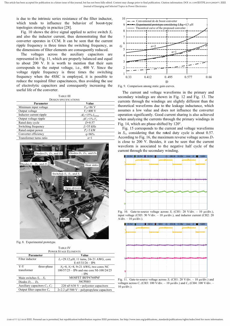
Firstly, the theoretical static gain curve of the dc-dc converter operating with 1/3<D<2/3 is compared with the one obtained experimentally in Fig. 9. The leakage inductance of the transformer, which is typically small and rated at Llkg=1.3 µH in this case, does not influence the conversion ratio significantly. The main difference between the curves for n=1
2168-6777 (c) 2018 IEEE. Personal use is permitted, but republication/redistribution requires IEEE permission. See http://www.ieee.org/publications_standards/publications/rights/index.html for more information.
This article has been accepted for publication in a future issue of this journal, but has not been fully edited. Content may change prior to final publication. Citation information: DOI 10.1109/JESTPE.2019.2892977, IEEEJournal of Emerging and Selected Topics in Power Electronics
is dwhtop
andconrippthe
repto corvolfreredof use
MOInORaSwRaCoTr
D
Fig
Fi
Ytra
MDAO
due to the inthich tends tpologies strongFig. 10 showd also the innverter operatple frequency
e dimensions oThe voltage
presented in Fiabout 200 V
rresponds to ltage ripple quency when
duce the requielectrolytic c
eful life of the
ParamMinimum input vo
utput voltage nductor current riputput voltage rippated duty cycle witching frequencated output poweonverter efficiencransformer turns
Diode
Diodes D1, D4, an
. 8. Experimenta
Parameterilter inductor
-Y thransformer
Main switches S1iodes D1 D9 uxiliary capacitorutput filter capac
trinsic series rto influence gly in practice
ws the drive sinductor currentes in CCM. y is three timof filter elemees across tig. 11, which V. It is worthe output vfrequency i
n the 4SSC ired filter capcapacitors an
e converter.
TAB
DESIGN SP
meter oltage
pple ple
cy er cy ratio
F
es D2, D5, and D8
nd D7
Switche
al prototype.
TAB
POWER STA
r L1=
ree-phase Np
100/
S3
rs C1, C2 2citor Co 22
resistance of the behavio
e [28]. gnal applied tnt, thus demoIt can be see
mes the switchents are conseqthe auxiliaryare properly b
rth to mentiovoltage, i.e., is three timis employed,acitances, thu
nd consequen
BLE III ECIFICATIONS
I
FPGA
Opto-drivers
Diodes D3,
s S1, S2, and S3
BLE IV AGE ELEMENTS
Va=29.12 H, 11 tur
E-65/33Np=8, Ns=8, 921 A
/57/25 – IP6 and –
MOSFET I30C
220 nF/630 V – p.2 µF/500 V – po
the filter induor of boost
to active switonstrating thaen that the cuhing frequencquently reducey capacitors balanced and on that their 400 V. Sinces the switc it is possib
us avoiding thntly increasing
Value VIN=86 V Vo=400 V
IL=15%IL(avg) Vo=1%Vo
D=0.57 fs=35 kHz Po=3 kW =96%
n=1
Heat sinks
D6, and D9
alue rns, 2421 AWG3/26 – IP6 AWG, two coresone core NI-100/IP6
IRFP4768PbF CPH03 polyester capacitolypropylene capa
uctor, t-type
tch S1 at the urrent cy, as ed.
are equal
sum e the ching
ble to he use g the
, core
NC /24/25
tors acitors
1
2
3
4
5
6
7
8
9
10
G
Fig. 9
ThsecocurretheorassumoperwhenFig.
Fiin SAccois clwavecurre
Fig. 1input A/div
Fig. 1voltag10 µs
0.33 0
0
Theoretic
ConventExperim
9. Comparison am
he current anndary windinents through tretical wavefomes a low v
ration significan analyzing th14, which areig. 15 corresp
S1, consideringording to Fig. lose to 200 Veform is assoent through th
10. Gate-to-sourvoltage (CH3: 5
v. – 10 µs/div.).
11. Gate-to-sourcges across C1 (CH/div.).
0.412 0
D
n=2
cal curve of the pro
tional dc-dc boost cmental prototype co
mong static gain c
nd voltage wngs are shownthe windings orms due to talue and doeantly. Good cuhe currents thre phase-shiftedponds to the cg that the rat16, the maxim
V. Besides, it ociated to th
he secondary w
rce voltage acros0 V/div. – 10 µs
ce voltage across H3: 100 V/div. –
0.495 0.
D
oposed converter
converteronsidering Llkg =1.
n=1
curves.
waveforms in n in Fig. 12 aare slightly d
the leakage ines not influenurrent sharingrough the primd by 120. current and voted duty cyclmum reverse vt can be seenhe negative hwinding.
ss S1 (CH1: 20 s/div.), and induc
s S1 (CH1: 20 V/d10 µs/div.) and C
577 0.
.3 µH
the primary and Fig. 13. Tdifferent than nductance, whnce the conveg is also achiemary winding
oltage wavefole is about 0voltage across
n that the currhalf cycle of
V/div. – 10 µs/dctor current (CH2
div. – 10 µs/div.)C2 (CH4: 100 V/d
.66
and The the
hich erter eved gs in
rms .57. s D7 rent the
div.), 2: 20
) and div. –
2168-6777 (c) 2018 IEEE. Personal use is permitted, but republication/redistribution requires IEEE permission. See http://www.ieee.org/publications_standards/publications/rights/index.html for more information.
This article has been accepted for publication in a future issue of this journal, but has not been fully edited. Content may change prior to final publication. Citation information: DOI 10.1109/JESTPE.2019.2892977, IEEEJournal of Emerging and Selected Topics in Power Electronics
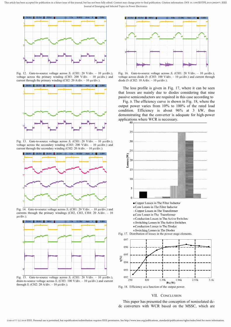
Figvoltcurr
Figvoltcurr
Figcurrµs/d
Figdraithro
. 12. Gate-to-sotage across the prent through the p
. 13. Gate-to-sotage across the srent through the s
. 14. Gate-to-sourents through thediv.).
. 15. Gate-to-soin-to-source voltaough S1 (CH2: 20
ource voltage acrprimary windingprimary winding
ource voltage acrsecondary windinsecondary windin
urce voltage acroe primary windin
ource voltage acrage across S1 (CH
0 A/div. – 10 µs/d
ross S1 (CH1: 20g (CH3: 200 V/d(CH2: 20 A/div.
ross S1 (CH1: 20ng (CH3: 200 V/ng (CH2: 20 A/div
oss S1 (CH1: 20 Vngs (CH2, CH3,
ross S1 (CH1: 20H3: 100 V/div. – div.).
0 V/div. – 10 µsdiv. – 10 µs/div– 10 µs/div.).
0 V/div. – 10 µs/div. – 10 µs/divv. – 10 µs/div.).
V/div. – 10 µs/div CH4: 20 A/div
0 V/div. – 10 µs10 µs/div.) and c
s/div.), v.) and
s/div.), v.) and
v.) and
v. – 10
s/div.), current
Fig. 1voltagdiode
Ththat passi
Fioutpconddemoappli
Fig. 1
0.
0.
0.
0.
0.
0.
Fig. 1
Thdc c
16. Gate-to-sourge across diode D D7 (CH2: 10 A/d
he loss profillosses are mive semiconduig. 3. The effiut power var
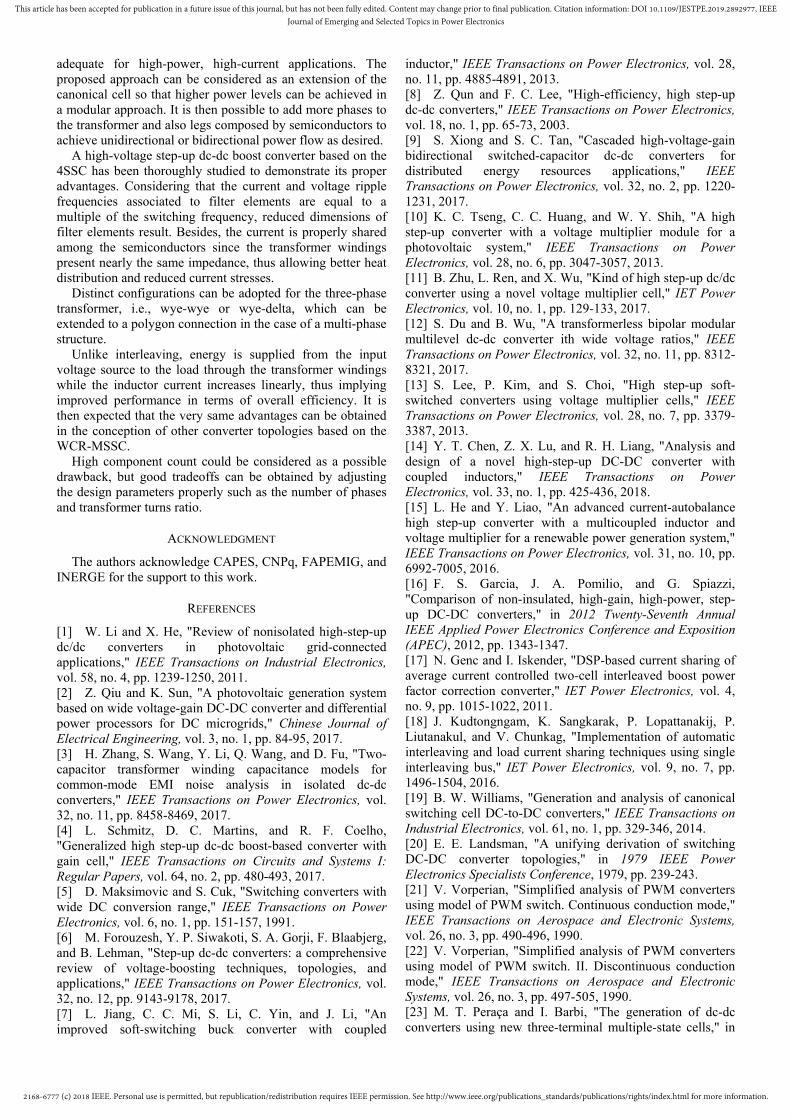
dition. Efficionstrating thaications where
7. Distribution o
250 8.92
.93
.94
.95
.96
.97
8. Efficiency as
his paper has converters wit
rce voltage acrosD7 (CH3: 100 V/ddiv. – 10 µs/div.).
e is given in mainly due to
uctors are requciency curve ries from 10%ency is ab
at the converte WCR is nec
of losses in the po
20 1.39kP
a function of the
VII. CON
presented theth WCR base
ss S1 (CH1: 20 div. – 10 µs/div..
Fig. 17, whediodes consi
uired in this cis shown in F
% to 100% obout 96% ater is adequatcessary.
ower stage elemen
1.96kPo (W)
e output power.
NCLUSION
e conception oed on the M
V/div. – 10 µs/d) and current thro
ere it can be sidering that n
case accordingFig. 18, whereof the rated lat 3 kW, te for high-po
nts.
2.53k
of nonisolated MSSC, which
div.), ough
seen nine g to the load thus wer
3.1k
dc-are
2168-6777 (c) 2018 IEEE. Personal use is permitted, but republication/redistribution requires IEEE permission. See http://www.ieee.org/publications_standards/publications/rights/index.html for more information.
This article has been accepted for publication in a future issue of this journal, but has not been fully edited. Content may change prior to final publication. Citation information: DOI 10.1109/JESTPE.2019.2892977, IEEEJournal of Emerging and Selected Topics in Power Electronics
adequate for high-power, high-current applications. The proposed approach can be considered as an extension of the canonical cell so that higher power levels can be achieved in a modular approach. It is then possible to add more phases to the transformer and also legs composed by semiconductors to achieve unidirectional or bidirectional power flow as desired.
A high-voltage step-up dc-dc boost converter based on the 4SSC has been thoroughly studied to demonstrate its proper advantages. Considering that the current and voltage ripple frequencies associated to filter elements are equal to a multiple of the switching frequency, reduced dimensions of filter elements result. Besides, the current is properly shared among the semiconductors since the transformer windings present nearly the same impedance, thus allowing better heat distribution and reduced current stresses.
Distinct configurations can be adopted for the three-phase transformer, i.e., wye-wye or wye-delta, which can be extended to a polygon connection in the case of a multi-phase structure.
Unlike interleaving, energy is supplied from the input voltage source to the load through the transformer windings while the inductor current increases linearly, thus implying improved performance in terms of overall efficiency. It is then expected that the very same advantages can be obtained in the conception of other converter topologies based on the WCR-MSSC.
High component count could be considered as a possible drawback, but good tradeoffs can be obtained by adjusting the design parameters properly such as the number of phases and transformer turns ratio.
ACKNOWLEDGMENT
The authors acknowledge CAPES, CNPq, FAPEMIG, and INERGE for the support to this work.
REFERENCES
[1] W. Li and X. He, "Review of nonisolated high-step-up dc/dc converters in photovoltaic grid-connected applications," IEEE Transactions on Industrial Electronics, vol. 58, no. 4, pp. 1239-1250, 2011. [2] Z. Qiu and K. Sun, "A photovoltaic generation system based on wide voltage-gain DC-DC converter and differential power processors for DC microgrids," Chinese Journal of Electrical Engineering, vol. 3, no. 1, pp. 84-95, 2017. [3] H. Zhang, S. Wang, Y. Li, Q. Wang, and D. Fu, "Two-capacitor transformer winding capacitance models for common-mode EMI noise analysis in isolated dc-dc converters," IEEE Transactions on Power Electronics, vol. 32, no. 11, pp. 8458-8469, 2017. [4] L. Schmitz, D. C. Martins, and R. F. Coelho, "Generalized high step-up dc-dc boost-based converter with gain cell," IEEE Transactions on Circuits and Systems I: Regular Papers, vol. 64, no. 2, pp. 480-493, 2017. [5] D. Maksimovic and S. Cuk, "Switching converters with wide DC conversion range," IEEE Transactions on Power Electronics, vol. 6, no. 1, pp. 151-157, 1991. [6] M. Forouzesh, Y. P. Siwakoti, S. A. Gorji, F. Blaabjerg, and B. Lehman, "Step-up dc-dc converters: a comprehensive review of voltage-boosting techniques, topologies, and applications," IEEE Transactions on Power Electronics, vol. 32, no. 12, pp. 9143-9178, 2017. [7] L. Jiang, C. C. Mi, S. Li, C. Yin, and J. Li, "An improved soft-switching buck converter with coupled
inductor," IEEE Transactions on Power Electronics, vol. 28, no. 11, pp. 4885-4891, 2013. [8] Z. Qun and F. C. Lee, "High-efficiency, high step-up dc-dc converters," IEEE Transactions on Power Electronics, vol. 18, no. 1, pp. 65-73, 2003. [9] S. Xiong and S. C. Tan, "Cascaded high-voltage-gain bidirectional switched-capacitor dc-dc converters for distributed energy resources applications," IEEE Transactions on Power Electronics, vol. 32, no. 2, pp. 1220-1231, 2017. [10] K. C. Tseng, C. C. Huang, and W. Y. Shih, "A high step-up converter with a voltage multiplier module for a photovoltaic system," IEEE Transactions on Power Electronics, vol. 28, no. 6, pp. 3047-3057, 2013. [11] B. Zhu, L. Ren, and X. Wu, "Kind of high step-up dc/dc converter using a novel voltage multiplier cell," IET Power Electronics, vol. 10, no. 1, pp. 129-133, 2017. [12] S. Du and B. Wu, "A transformerless bipolar modular multilevel dc-dc converter ith wide voltage ratios," IEEE Transactions on Power Electronics, vol. 32, no. 11, pp. 8312-8321, 2017. [13] S. Lee, P. Kim, and S. Choi, "High step-up soft-switched converters using voltage multiplier cells," IEEE Transactions on Power Electronics, vol. 28, no. 7, pp. 3379-3387, 2013. [14] Y. T. Chen, Z. X. Lu, and R. H. Liang, "Analysis and design of a novel high-step-up DC-DC converter with coupled inductors," IEEE Transactions on Power Electronics, vol. 33, no. 1, pp. 425-436, 2018. [15] L. He and Y. Liao, "An advanced current-autobalance high step-up converter with a multicoupled inductor and voltage multiplier for a renewable power generation system," IEEE Transactions on Power Electronics, vol. 31, no. 10, pp. 6992-7005, 2016. [16] F. S. Garcia, J. A. Pomilio, and G. Spiazzi, "Comparison of non-insulated, high-gain, high-power, step-up DC-DC converters," in 2012 Twenty-Seventh Annual IEEE Applied Power Electronics Conference and Exposition (APEC), 2012, pp. 1343-1347. [17] N. Genc and I. Iskender, "DSP-based current sharing of average current controlled two-cell interleaved boost power factor correction converter," IET Power Electronics, vol. 4, no. 9, pp. 1015-1022, 2011. [18] J. Kudtongngam, K. Sangkarak, P. Lopattanakij, P. Liutanakul, and V. Chunkag, "Implementation of automatic interleaving and load current sharing techniques using single interleaving bus," IET Power Electronics, vol. 9, no. 7, pp. 1496-1504, 2016. [19] B. W. Williams, "Generation and analysis of canonical switching cell DC-to-DC converters," IEEE Transactions on Industrial Electronics, vol. 61, no. 1, pp. 329-346, 2014. [20] E. E. Landsman, "A unifying derivation of switching DC-DC converter topologies," in 1979 IEEE Power Electronics Specialists Conference, 1979, pp. 239-243. [21] V. Vorperian, "Simplified analysis of PWM converters using model of PWM switch. Continuous conduction mode," IEEE Transactions on Aerospace and Electronic Systems, vol. 26, no. 3, pp. 490-496, 1990. [22] V. Vorperian, "Simplified analysis of PWM converters using model of PWM switch. II. Discontinuous conduction mode," IEEE Transactions on Aerospace and Electronic Systems, vol. 26, no. 3, pp. 497-505, 1990. [23] M. T. Peraça and I. Barbi, "The generation of dc-dc converters using new three-terminal multiple-state cells," in

2168-6777 (c) 2018 IEEE. Personal use is permitted, but republication/redistribution requires IEEE permission. See http://www.ieee.org/publications_standards/publications/rights/index.html for more information.
This article has been accepted for publication in a future issue of this journal, but has not been fully edited. Content may change prior to final publication. Citation information: DOI 10.1109/JESTPE.2019.2892977, IEEEJournal of Emerging and Selected Topics in Power Electronics
PoIEE[24"PearcTra473[25FormuPo[26ChconInd[27inteindEle[28pascon195
uninDr. (SO
wer ElectronEE 36th, 20054] H. Choi, Merformance ochitecture utilansactions on3, 2015. 5] G. Mademrward-based c
ultistage-stackwer Electroni
6] L. Po-Wa, heng, "Steadynverter with dustrial Electr7] W. Li anerleaved boo
ductors and reectronics, vol.8] Y. Hu, Y. ssive absorptinverter," IET 53, 2014.
nterruptible poweBastos is a me
OBRAEP).
nics Specialist5, pp. 2657-26M. Ciobotaru,of medium-vlizing high-g
n Sustainable
mlis, G. K. Scontrol in a
ked boost archics, vol. 32, noL. Yim-Shu,
y-state analycoupled indu
ronics, vol. 47nd X. He, ost convertereduced auxilia. 2, no. 2, pp.
Deng, J. Loion circuit usePower Electr
BIOGR
George Hathe the B.ScengineeringFortaleza, respectivelyCurrently, hFederal InTechnologyresearch insupplies, p
er systems, and reember of the B
Levy Ferredegree in elUniversity othe M.S. dFederal Univ
ts Conference663. , M. Jang, anvoltage DC-
gain DC-DC Energy, vol.
Steinke, and dc-dc conver
hitecture," IEEo. 2, pp. 1507-, D. K. W. Cysis of an uctors," IEEE7, no. 4, pp. 78"High step-urs with crosary switch nu125-133, 2009
ong, and X. Led in non-isoronics, vol. 7
RAPHIES
arrison de Alcâc., M.Sc., and Phg from the Federa
Brazil in 200y. he is an Associ
nstitute of Eduy of Ceará, Caunterests includepower factor cenewable energy
Brazilian Society
ira Costa (SM’lectrical enginee
of Ceara, Fortalezegree in powerversity of Santa C
e, 2005. PES
nd V. G. Age-bus PV syconverter," I6, no. 2, pp.
A. Rufer, "Frter of asymmEE Transactio-1517, 2017.
Cheng, and L. interleaved b
E Transaction87-795, 2000.up soft switcss-winding-couumber," IET P9. Lu, "High ste
olated high ste7, no. 8, pp. 1
ntara Bastos re.D. degrees in eleal University of 1, 2005, and
ate Professor wiucation, Sciencecaia, Brazil. His
switch-mode correction technsystems. of Power Elect
14) received theering from the Fza, Brazil, in 20
electronics froCatarina, Florian
SC'05.
elidis, ystem IEEE 464-
Feed-metric ons on
Xiu-boost
ns on ching upled
Power
ep-up ep-up 1945-
eceived ectrical Ceará, 2017,
ith the e, and s main power
niques,
tronics
e B.Sc. Federal 10 and
om the nópolis,
BrazilElectrpowerthe chUnivewith includconve
convesystem
and Tnew hHis mplatfo
Cearápowerrenew
l, in 2013. He wric, Joinville, Brar supply systems.hair of power eleersity, Kiel, GermABB Corporate de modular converter topologies fo
ersion range, noms.
Technology AB, Khigh-efficiency (H
main research areaorms with HE top
á, Fortaleza, Brazr factor correcti
wable energy syste
was a power elecazil from 2013 to. From 2014 to 20ctronics at the Cmany. He is currResearch, Switz
verter designs, dor industrial and r
Fernando Leand Ph.D. degFederal UnivBrazil, in 1999
Currently, heUniversity of Brazil. His resrelated issuenonsolated dc
ovel converter
Grover Victothe B.Sc. degrSimón Univerand the M.Sengineering frCatarina, Florrespectively.
Since July 20Engineer with
Kista, Sweden, whHE) circuit topoloas are in industriaologies for high-p
René Pastordegree in elUniversity, the M.Sc. engineering Catarina, Florespectively
Currently, hof Electrical
zil. His main reseion techniques, ems.
ctronics design eto 2014, working018, he was a Re
Christian-Albrechtrently a power e
zerland. His curredc–dc converters,renewable energy
essa Tofoli receivgrees in electrical versity of Ube9, 2002, and 2005
e is a Professof São João del-Research interests ines, high-powerc-dc converters topologies, and
or Torrico-Bascree in electrical ersity, CochabambSc. and PhD dfrom the Federal rianópolis, Brazil
009, he has beh GTB Power E
where he is a Consogies to the poweal power electronpower and green
r Torrico-Bascolectrical engineerCochabamba, B
and PhD defrom the Federa
orianópolis, Brazy.
he is a Professor al Engineering, Fearch interests inc
uninterruptible
engineer at Schneg with uninterrupesearch Assistant ts Universität zu electronics researent research inte, and high-efficiy applications.
ved the B.Sc., Mengineering from
erlândia, Uberlân5, respectively.
or with the Fedei, São João del-nclude power-quar factor rectif
with wide vold solar photovo
opé (M’04) receengineering fromba, Bolivia, in 1degrees in elect
University of Sl, in 1996 and 2
en a Senior DeElectronics Resesultant and is offeer electronic indunics and creating energy applicatio
opé received the Bring from San Si
Bolivia, in 1992, egrees in electal University of Szil, in 1994 and 2
with the DepartmFederal Universitclude power supppower systems,
eider ptible with Kiel
rcher erests ency
M.Sc., m the ndia,
deral -Rei, ality-fiers, ltage
oltaic
eived m San 1993, trical Santa 2001,
esign earch ering ustry.
new ons.
B.Sc. imón
and trical Santa 2000,
ment ty of plies,
and