Nondestructive 3D X-ray imaging for advanced …...Nondestructive 3D XRM tomographic imaging was...
4
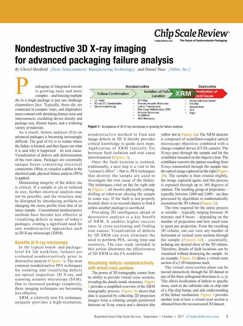
1 Reprinted from Chip Scale Review September • October • 2017 [ChipScaleReview.com] ackaging of integrated circuits is growing more and more complex – and housing multiple die in a single package is just one challenge chipmakers face. Typically, these die are connected in complex ways, and chipmakers must contend with shrinking feature sizes and interconnects, escalating device density and package size, thinner layers, and a widening variety of materials. As a result, failure analysis (FA) on advanced packages is becoming increasingly difficult. The goal of FA is to isolate where it is and why it happened – its root cause. Visualization of defects aids determination of the root cause. Packages are essentially opaque boxes containing electrical connections. Often, to visualize a defect in the electrical path, physical failure analysis (PFA) is applied. Maintaining integrity of the defect site is critical. If a sample is cut or reduced in size, further electrical analysis may not be possible, and the structure may be disrupted by introducing artifacts or changing the stress profile from that of an intact sample. Conventional nondestructive methods have become less effective at visualizing defects in many of today’s packages, creating a significant need for new nondestructive approaches such as 3D X-ray microscopy (XRM). Benefits of X-ray microscopy In the typical board- and package- level FA lab workflow, failures are evaluated nondestructively prior to destructive analysis (Figure 1). The most common nondestructive PFA techniques for isolating and visualizing defects are optical inspection, 2D X-ray, and scanning acoustic microscopy (SAM). Due to increased package complexity, these imaging techniques are becoming less effective. XRM, a relatively new FA technique, uniquely provides a high-resolution, nondestructive method to find and image defects in 3D. It thereby provides critical knowledge to guide next steps. Application of XRM typically fits between fault isolation and root cause determination (Figure 1). Once the fault location is isolated, traditionally, a next step is a visit to the that destroy the sample are used to investigate the root cause of the failure. The techniques cited on the far right side in Figure 1 all involve physically cutting, drilling or otherwise altering the sample in some way. If the fault is not properly Providing 3D intelligence ahead of destructive analysis is a key benefit of XRM. It enables higher success rates in cross-sectioning and finding root causes. Visualization of defects by 3D XRM can even eliminate the need to perform PFA, saving time and resources. The case study included in this article illustrates the effectiveness of 3D XRM in the FA workflow. Visualizing defects nondestructively with virtual cross sections The power of 3D tomography comes from its ability to provide virtual cross sections, revealing the details inside structures. Figure 2 tomography process. Figure 2a shows that data is acquired by collecting 2D projection images from a rotating sample positioned between an X-ray source and a detector (the yellow dot in Figure 2a ). The XRM detector is composed of scintillator-coupled optical microscope objectives combined with a charge-coupled device (CCD) camera. The X-rays pass through the sample and hit the scintillator mounted on the objective lens. The scintillator converts the pattern resulting from X-rays transmitted through the sample into the optical image captured on the right ( Figure 2b). The sample is then rotated slightly, the image captured again, and this process is repeated through up to 360 degrees of rotation. The resulting group of projections – typically, between 1,000 and 2,000 – are then processed by algorithms to mathematically reconstruct the 3D volume (Figure 2c ). The time required for the entire process is variable – typically ranging between 30 minutes and 8 hours – depending on the number of projections and how much time is spent per projection. From the resulting 3D volume, one can view any number of horizontal or vertical cross sections through the sample ( Figure 2d) – essentially, isolating any desired sliver of the 3D volume. Therefore, details of fault locations can be visualized without destroying the sample. As an example, Figure 2d shows a virtual cross section of a 2.5D interposer stack. The virtual cross-section plane can be moved interactively through the 3D dataset in any of the three orthogonal directions (x, y, z). areas, such as the substrate-side or chip-side of a flip-chip bump, and aids understanding of the failure mechanism. Figure 3 provides another look at how a virtual cross section is obtained from the reconstructed 3D dataset. P Figure 1: Acceptance of 3D X-ray microscopy is growing for failure analysis. Nondestructive 3D X-ray imaging for advanced packaging failure analysis [Zeiss Semiconductor Manufacturing Technology], and Daniel Nuez [Xilinx, Inc.]
Transcript of Nondestructive 3D X-ray imaging for advanced …...Nondestructive 3D XRM tomographic imaging was...
11Reprinted from Chip Scale Review September • October • 2017 [ChipScaleReview.com]
ackaging of integrated circuits is growing more and more complex – and housing multiple
die in a single package is just one challenge chipmakers face. Typically, these die are connected in complex ways, and chipmakers must contend with shrinking feature sizes and interconnects, escalating device density and package size, thinner layers, and a widening variety of materials.
As a result, failure analysis (FA) on advanced packages is becoming increasingly difficult. The goal of FA is to isolate where
it is and why it happened – its root cause. Visualization of defects aids determination of the root cause. Packages are essentially opaque boxes containing elect r ical connections. Often, to visualize a defect in the electrical path, physical failure analysis (PFA) is applied.
Maintaining integrity of the defect site is critical. If a sample is cut or reduced in size, further electrical analysis may not be possible, and the structure may be disrupted by introducing artifacts or changing the stress profile from that of an intact sample. Conventional nondestructive methods have become less effective at visualizing defects in many of today’s packages, creating a significant need for new nondestructive approaches such as 3D X-ray microscopy (XRM).
Bene�ts of X-ray microscopyIn the typical board- and package-
level FA lab workf low, failures are evaluated nondest ruct ively pr ior to destructive analysis (Figure 1). The most common nondestructive PFA techniques for isolating and visualizing defects are optical inspection, 2D X-ray, and scanning acoustic microscopy (SAM). Due to increased package complexity, these imaging techniques are becoming less effective.
XRM, a relatively new FA technique, uniquely provides a high-resolution,
nondest r uct ive method to f ind and image defects in 3D. It thereby provides critical knowledge to guide next steps. Appl icat ion of XR M typical ly f it s between fault isolation and root cause determination (Figure 1).
Once the fault location is isolated, traditionally, a next step is a visit to the
that dest roy the sample are used to investigate the root cause of the failure. The techniques cited on the far right side in Figure 1 all involve physically cutting, drilling or otherwise altering the sample in some way. If the fault is not properly
Providing 3D intelligence ahead of destructive analysis is a key benef it of XRM. It enables h igher success rates in cross-sectioning and f inding root causes. Visualization of defects by 3D XRM can even eliminate the need to perform PFA, saving time and resources. The case study included in this article illustrates the effectiveness of 3D XRM in the FA workf low.
Visualizing defects nondestructively with virtual cross sections
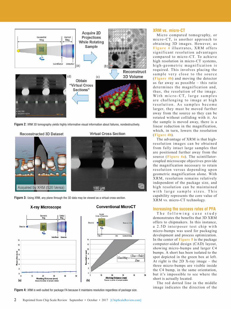
The power of 3D tomography comes from its ability to provide virtual cross sections, revealing the details inside structures. Figure 2tomography process. Figure 2a shows that data is acquired by collecting 2D projection images from a rotating sample positioned between an X-ray source and a detector (the
yellow dot in Figure 2a). The XRM detector is composed of scintillator-coupled optical microscope objectives combined with a charge-coupled device (CCD) camera. The X-rays pass through the sample and hit the scintillator mounted on the objective lens. The scintillator converts the pattern resulting from X-rays transmitted through the sample into the optical image captured on the right (Figure 2b). The sample is then rotated slightly, the image captured again, and this process is repeated through up to 360 degrees of rotation. The resulting group of projections – typically, between 1,000 and 2,000 – are then processed by algorithms to mathematically reconstruct the 3D volume (Figure 2c).
The time required for the entire process is variable – typically ranging between 30 minutes and 8 hours – depending on the number of projections and how much time is spent per projection. From the resulting 3D volume, one can view any number of horizontal or vertical cross sections through the sample (Figure 2d) – essentially, isolating any desired sliver of the 3D volume. Therefore, details of fault locations can be visualized without destroying the sample. As an example, Figure 2d shows a virtual cross section of a 2.5D interposer stack.
The virtual cross-section plane can be moved interactively through the 3D dataset in any of the three orthogonal directions (x, y, z).
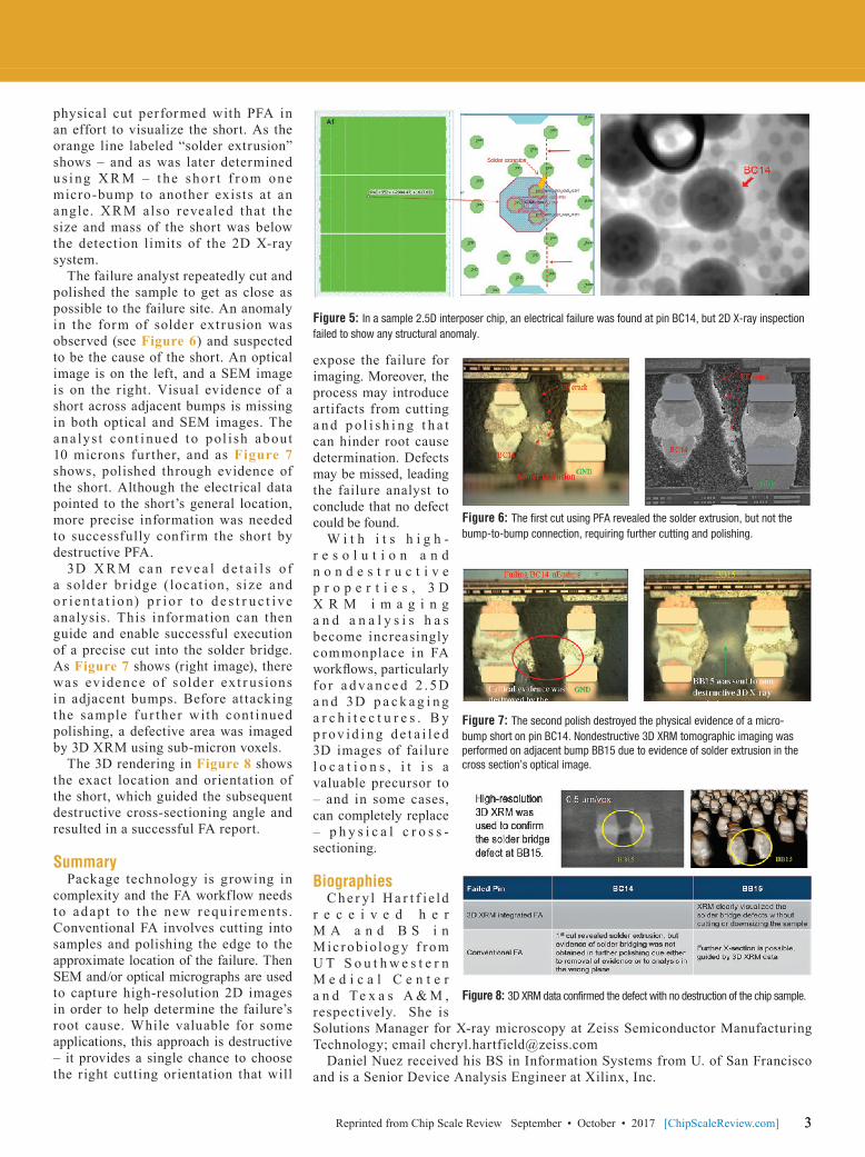
areas, such as the substrate-side or chip-side of a flip-chip bump, and aids understanding of the failure mechanism. Figure 3 provides another look at how a virtual cross section is obtained from the reconstructed 3D dataset.
PFigure 1: Acceptance of 3D X-ray microscopy is growing for failure analysis.
Nondestructive 3D X-ray imaging for advanced packaging failure analysis
[Zeiss Semiconductor Manufacturing Technology], and Daniel Nuez [Xilinx, Inc.]
22 Reprinted from Chip Scale Review September • October • 2017 [ChipScaleReview.com]
XRM vs. micro-CTMicro computed tomography, or
m ic ro - CT, i s anothe r approach to obtain ing 3D images. However, as Fig ure 4 i l lu s t r a t e s , X R M of fe r s s ig n i f ica nt r e solu t ion a dva nt ages compared to micro-CT. To achieve high resolution in micro-CT systems, h ig h - ge o m e t r i c m a g n i f i c a t io n i s required. This involves placing the s a m pl e ve r y c lo s e t o t h e s o u r c e (Figure 4b) and moving the detector as far away as possible – this rat io deter mines the magnif icat ion and , t hus , t he resolut ion of t he image. W i t h m i c r o - C T, l a r g e s a m p l e s a r e cha l le ng i ng t o i m age a t h ig h r e s o l u t i o n . A s s a m p l e s b e c o m e larger, they must be moved fur ther away from the source so they can be rotated without colliding with it. As the sample is moved away, there is a linear reduction in the magnification, which, in turn, lowers the resolution (Figure 4b).
The advantage of XRM is that high-resolut ion images can be obtained from fully intact large samples that are positioned further away from the source (Figure 4a). The scintillator-coupled microscope objectives provide the magnification necessary to retain resolut ion ver sus depend ing upon geometric magnif ication alone. With XRM, resolution remains relat ively independent of the package size, and h igh resolut ion can be maintained w i t h l a r g e s a m p l e s i z e s . T h i s capability represents the core value of XRM vs. micro-CT technology.
Increasing the success rates of PFAT h e f o l l o w i n g c a s e s t u d y
demonstrates the benefits that 3D XRM offers to chipmakers. In this instance, a 2 . 5 D i n t e r p o s e r t e s t ch ip w i t h micro-bumps was used for packaging development and process optimization. In the center of Figure 5 is the package computer-aided design (CAD) layout, showing micro-bumps and larger C4 bumps. A short has been isolated to the spot depicted in the green box at left. At right is the 2D X-ray image – the three micro-bumps are visible inside the C4 bump, in the same orientation, but it’s impossible to see where the short is actually located.
The red dot ted line in the middle image indicates the direction of the
Figure 2: XRM 3D tomography yields highly informative visual information about failures, nondestructively.
Figure 3: Using XRM, any plane through the 3D data may be viewed as a virtual cross section.
Figure 4: XRM is well-suited for package FA because it maintains resolution regardless of package size.
33Reprinted from Chip Scale Review September • October • 2017 [ChipScaleReview.com]
physical cut performed with PFA in an effort to visualize the short. As the orange line labeled “solder extrusion” shows – and as was later determined u s i ng X R M – t he shor t f rom one micro-bump to another exists at an angle. XR M also revealed that the size and mass of the short was below the detection limits of the 2D X-ray system.
The failure analyst repeatedly cut and polished the sample to get as close as possible to the failure site. An anomaly in the form of solder extrusion was observed (see Figure 6) and suspected to be the cause of the short. An optical image is on the left, and a SEM image is on the right. Visual evidence of a short across adjacent bumps is missing in both optical and SEM images. The ana lys t cont i nued to pol i sh about 10 microns fur ther, and as Figure 7 shows, polished through evidence of the short. Although the electrical data pointed to the short’s general location, more precise information was needed to successfully confirm the short by destructive PFA.
3D X R M c a n r e ve a l d e t a i l s of a solder br idge ( locat ion, size and o r i e n t a t io n) p r io r t o d e s t r u c t ive analysis. This information can then guide and enable successful execution of a precise cut into the solder bridge. As Figure 7 shows (right image), there was ev idence of solder ext r usions in adjacent bumps. Before at tacking the sample f u r ther with cont inued polishing, a defective area was imaged by 3D XRM using sub-micron voxels.
The 3D rendering in Figure 8 shows the exact location and orientation of the short, which guided the subsequent destructive cross-sectioning angle and resulted in a successful FA report.
SummaryPackage technology is growing in
complexity and the FA workflow needs to adapt to the new requi rements . Conventional FA involves cutting into samples and polishing the edge to the approximate location of the failure. Then SEM and/or optical micrographs are used to capture high-resolution 2D images in order to help determine the failure’s root cause. While valuable for some applications, this approach is destructive – it provides a single chance to choose the right cutting orientation that will
expose the failure for imaging. Moreover, the process may introduce artifacts from cutting a n d p o l i s h i n g t h a t can hinder root cause determination. Defects may be missed, leading the failure analyst to conclude that no defect could be found.
W i t h i t s h i g h -r e s o l u t i o n a n d n o n d e s t r u c t i v e p r o p e r t i e s , 3 D X R M i m a g i n g a n d a n a l y s i s h a s become increasingly commonplace in FA workflows, particularly fo r a d v a n c e d 2 . 5 D a n d 3D p a c k a g i n g a r c h i t e c t u r e s . B y p r ov id i n g d e t a i l e d 3D images of failure l o c a t i o n s , i t i s a valuable precursor to – and in some cases, can completely replace – p h y s i c a l c r o s s -sectioning.
BiographiesC he r y l H a r t f i e ld
r e c e i v e d h e r M A a n d B S i n M ic robiolog y f rom U T S o u t h w e s t e r n M e d i c a l C e n t e r a n d Te x a s A & M , respectively. She is Solutions Manager for X-ray microscopy at Zeiss Semiconductor Manufacturing Technology; email [email protected]
Daniel Nuez received his BS in Information Systems from U. of San Francisco and is a Senior Device Analysis Engineer at Xilinx, Inc.
Figure 5: In a sample 2.5D interposer chip, an electrical failure was found at pin BC14, but 2D X-ray inspection failed to show any structural anomaly.
Figure 6: The first cut using PFA revealed the solder extrusion, but not the bump-to-bump connection, requiring further cutting and polishing.
Figure 7: The second polish destroyed the physical evidence of a micro-bump short on pin BC14. Nondestructive 3D XRM tomographic imaging was performed on adjacent bump BB15 due to evidence of solder extrusion in the cross section’s optical image.
Figure 8: 3D XRM data confirmed the defect with no destruction of the chip sample.

Carl ZEISS SMT PCS Group4385 Hopyard RoadPleasanton, CA 94588 USA www.zeiss.com/pcs
Repr
inte
d by
Car
l Zei
ss S
MT
with
per
mis
sion
fro
m C
hip
Scal
e Re
view
.©
201
7 C
hip
Scal
e Re
view