NON-EQUILIBRIUM GREEN'S FUNCTIONS IN - …ee.ucr.edu/~rlake/dresden02_final_unix.pdf ·...
18
-
Upload
hoangduong -
Category
Documents
-
view
214 -
download
0
Transcript of NON-EQUILIBRIUM GREEN'S FUNCTIONS IN - …ee.ucr.edu/~rlake/dresden02_final_unix.pdf ·...

NON-EQUILIBRIUM GREEN'S FUNCTIONS IN
SEMICONDUCTOR DEVICE MODELING
ROGER LAKE
Department of Electrical Engineering, University of California, Riverside, CA
92521-0204
E-mail: [email protected]
DEJAN JOVANOVIC
Motorola, Physical Sciences Research Laboratories, 4200 W. Jemez Rd. Suite
300, Los Alamos, NM 87544
E-mail: [email protected]
CRISTIAN RIVAS
Department of Electrical Engineering, University of California, Riverside, CA
92521-0204 and Eric Jonsson School of Engineering, University of Texas at
Dallas, Richardson, TX 75083
E-mail: [email protected]
We present an overview of semiconductor device modeling using non-equilibriumGreen function techniques. The various e�orts and their associated goals, prob-lems, and solutions tend to naturally divide according to the dimensionality, 1D,2D, or 3D, of the transport which we use to classify and organize the discussion.Our current e�orts are largely focused on 2D and 3D modeling. The theory andapproach laid out for 1D serves as the basis for 2D and 3D.
1. Introduction
Over the last decade, non-equilibrium Green's function (NEGF) techniques
have become widely used in corporate, engineering, government, and aca-
demic laboratories for modeling high-bias, quantum electron and hole trans-
port in wide variety of materials and devices: ultra-scaled Si MOSFETs1;2,
Si / SixGe1�x tunnel diodes3, In0:47Ga0:53As / In0:52Al0:48As / InAs /
AlAs high electron mobility transistors (HEMTs) and resonant tunneling
diodes (RTDs)4, InAs / AlSb / GaSb HEMTs and RTDs, quantum well
infrared photodetectors (QWIPs), Si / SixGe1�x quantum dots, carbon
nanotubes5, and organic molecular wires6. The physics that have been in-
cluded are open-system boundaries, full-bandstructure, bandtails, Hartree
1

2
and exchange-correlation potentials within a local density approximation
(LDA), acoustic, optical, intra-valley, inter-valley, and inter-band phonon
scattering, alloy disorder and interface roughness scattering in Born type
approximations3;7, photon absorption and emission, one, two and three di-
mensional spatially varying potentials, energy and heat transport8, single
electron charging9, shot noise, D.C., A.C., and transient response.
E�ort developing a quantum semiconductor device simulator for devices
in which the potential varies along one dimension (1D) peaked during Texas
Instruments' Nanotechnology Engineering program which ran from 1993-
1997 and resulted in the the Nanoelectronic Engineering Modeling (NEMO)
program10. Recent developments are the modeling of the inter-valley, inter-
band, phonon-assisted tunneling current in Si / SixGe1�x tunnel diodes3.
Development of quantum semiconductor device simulators for devices in
which the potential varies in two and three dimensions (2D and 3D) are cur-
rently underway1;2. The primary objective of the 2D development e�ort has
been the modeling of ultra- scaled Si based FETs. These simulators treat
the bandstructure in a multiple single-band model which includes 3 decou-
pled bands to account for the three non-equivalent valleys in the quantized
channel. The simulators have included Hartree quantum charge self- consis-
tency, and open system boundary conditions at the source, drain, and gate.
Empirical, elastic, incoherent scattering models have been implemented.
Our primary objective of the 3D development e�ort is the modeling of
strained Si / SiGe quantum dots. A full bandstructure nearest neighbor
sp3s�d5 model is used. Both the 2D and 3D simulators make use of large
scale parallel computing.
2. One Dimensional Simulators
Texas Instruments' Nanotechnology Engineering program gave rise to the
largest e�ort to date to create a one dimensional, general, quantum semi-
conductor device simulator resulting in the software known as NEMO10. A
detailed account of the theory is given by Lake et al.7 This basic approach
serves as the basis for 2D and 3D simulators. The equations such as those
for the current, the electron density, and the recursive Green function algo-
rithm (Sec. IV of [6]) are directly used in 2D and 3D simulators by letting
the block-matrix Green functions represent a line of sites or atoms in 2D
or a plane of atoms or sites in 3D. The core approach of partitioning a
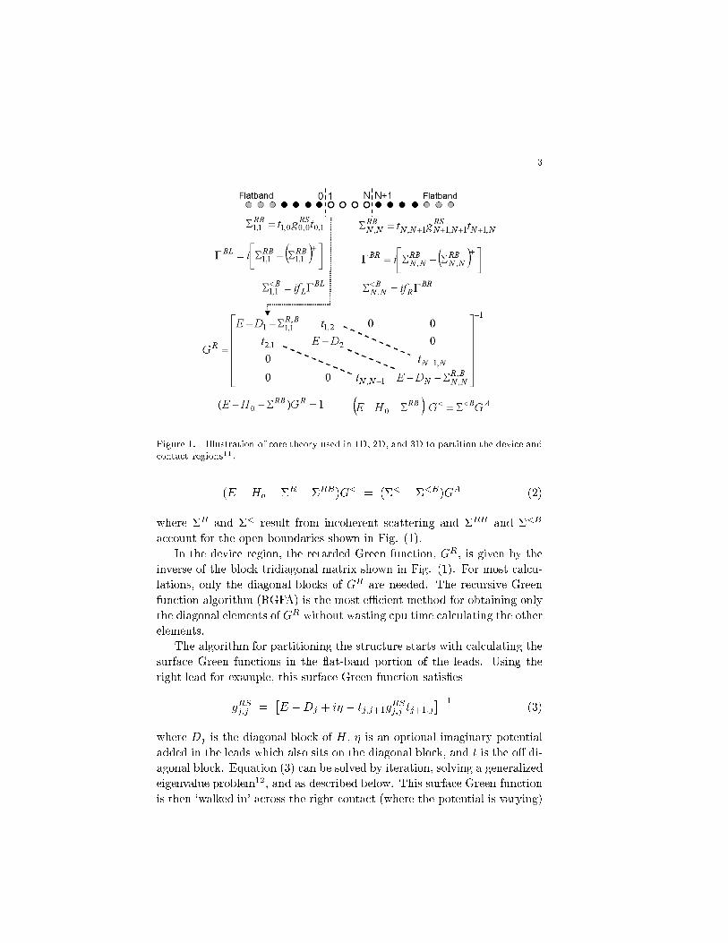
structure into contact and device regions is illustrated in Fig. (1). In the
central device region, the equations of motion for GR and G< are
(E �Ho ��R � �RB)GR = 1 (1)
3
Figure 1. Illustration of core theory used in 1D, 2D, and 3D to partition the device andcontact regions11.
(E �Ho ��R ��RB)G< = (�< +�<B)GA (2)
where �R and �< result from incoherent scattering and �RB and �<B
account for the open boundaries shown in Fig. (1).
In the device region, the retarded Green function, GR, is given by the
inverse of the block tridiagonal matrix shown in Fig. (1). For most calcu-
lations, only the diagonal blocks of GR are needed. The recursive Green
function algorithm (RGFA) is the most eÆcient method for obtaining only
the diagonal elements of GR without wasting cpu time calculating the other
elements.
The algorithm for partitioning the structure starts with calculating the
surface Green functions in the at-band portion of the leads. Using the
right lead for example, this surface Green function satis�es
gRSj;j =�E �Dj + i� � tj;j+1g
RSj;j tj+1;j
��1(3)
where Dj is the diagonal block of H , � is an optional imaginary potential
added in the leads which also sits on the diagonal block, and t is the o� di-
agonal block. Equation (3) can be solved by iteration, solving a generalized
eigenvalue problem12, and as described below. This surface Green function
is then `walked in' across the right contact (where the potential is varying)

4
up to site N + 1 using the recursive Green function algorithm
gBRj;j =�E �Dj �+i� � tj;j+1g
BRj+1;j+1tj+1;j
��1(4)
where the B superscript indicates that this surface retarded Green function
is connected to the right. This gives the surface Green function at site
N + 1 in Fig. (1). We now continue to walk this surface Green function
across the device. The only di�erence is that in the device, � = 0, and, if
a retarded self energy exists due to incoherent scattering which is block-
diagonal or block-tridiagonal, then it is simply added to the diagonal, D,
and o� diagonal, t, blocks in Eq. (4). If the retarded self energy is a full
matrix, such as for polar optical phonons, then the full GR is required and
the recursive Green function algorithm cannot be used.
If a quantum self-consistent calculation of the charge and potential is
desired, then one continues walking the right connected Green function all
the way across the left contact to the left at band region, say site index
-5 as illustrated in Fig. (1). There, one creates the exact Green function
from
GR�5;�5 =
�E �D�5 + i� � t�5;�4g
BR�4;�4t�4;�5 � t�5;�6g
RSt�6;�5
��1(5)
where gRS is the at-band surface Green function of the left lead calculated
similarly to the at-band surface Green function of the right lead. One
then sweeps back across the structure from left to right creating the exact
diagonal block of the Green function of the entire structure.
GRj;j = gBRj;j + gBRj;j tj;j�1G
Rj�1;j�1tj�1;jg
BRj;j (6)
Equations (4) - (6) form the RGFA for both GR and GA.
The recursive Green function algorithm for G<, discussed below, was
also developed during the NEMO program (by D.J.), and was implemented
in both 1D and 2D prototype codes but did not make it into the �nal
NEMO software. Below we write down a basic set of equations from [6]
that form the basis of device modeling.
The general expression for the current is
J =e
~
ZdE
2�Tr��BL
�fLA + iG<
� ; (7)
and the expression for the coherent current is
J =e
~
ZdE
2�Tr��BL
�A � AL
�(fL � fR) : (8)
The coherent diagonal elements of G< required for the electron density are
�iG< = fLAL + fR
�A�AL
�(9)

5
where
AL = GR�BLGA : (10)
In Eqs. (1) - (10), the superscript and subscript L represents a quantity in-
jected from the left contact; R the right contact. The trace is over all atoms
and orbitals and includes a sum over transverse momentum depending on
the dimensionality.
We break the discussion down following the natural partitioning of the
Hamiltonian shown in Eq. (11).
H = Ho + Hpop + Hac + Hir + Hal + Hii| {z }H�
(11)
Ho contains the kinetic energy, the crystal potential, the self-consistent
Hartree potential calculated from Poisson's equation, and a local density
expression for the exchange correlation potential. In the above approxima-
tions, the last two potentials resulting from the e-e interaction only shift
the on-site orbital energies and must be calculated self consistently. The
remainder of the terms represent scattering potentials which are included
through a self-energy in Born type approximations: polar-optical phonon,
acoustic phonon, interface roughness, alloy disorder, and ionized impurity.
These self-energies are non-Hermitian.
The basis set for all of the band structure models is a planar-orbital basis
with the di�erence lying in the number of orbitals per atom. We considered
the planar-orbital models to be the most versatile for modeling devices in
which the X or L valley played a role in the electron tansport. They also
allow one to explicitly look at interface roughness and alloy disorder since
each atomic layer is represented.
One of the most useful developments that occurred during the NEMO
project was the development and implementation of what we referred to as
the generalized open system boundary conditions 7;13;14 which include the
e�ects of the contacts on the device included exactly through a self-energy,
�B . The boundary conditions were developed to reduce the device domain
for the computationally intensive calculations required to include incoherent
scattering. However, we quickly found them to be crucial for most coherent
transport problems in which injection into the `device' comes from quasi-
bound states in one or both contacts such as occur in the emitter of an
RTD or the gate leakage current from the inversion layer of a MOSFET or
the accumulation layer of a HEMT4. For such situations, it is necessary
to include a �nite imaginary potential in the contacts to account for the
energy broadening of the contact states.
6
The scattering components of the Hamiltonian, H�, of Eq. (11) are
treated in Born type of approximations ranging from multiple sequential
scattering to self-consistent Born7. For inelastic scattering, the multiple se-
quential scattering algorithm is a low-density approximation in which Pauli
exclusion is ignored. The real strength of the multiple sequential scatter-
ing algorithm is that it always conserves current. In contrast, the self-
consistent Born approximation only conserves current once self-consistency
is achieved.
The simplest scattering mechanisms to implement from a computa-
tional perspective are alloy disorder, acoustic phonons in the elastic, high-
temperature approximation, and interface roughness. In our level of
approximation7 all mechanisms result in self energies which have only non-
zero diagonal blocks (or diagonal elements in single band models). Further-
more, only the interface roughness self-energy has a transverse momentum
dependence.
Polar optical phonon scattering results in a self energy that is a full
matrix with strong transverse momentum dependence. We implemented a
bulk phonon model in a single sequential scattering approximation. The
correct momentum dependence and non-locality of the self-energy were re-
tained, and Pauli-exclusion was sacri�ced.
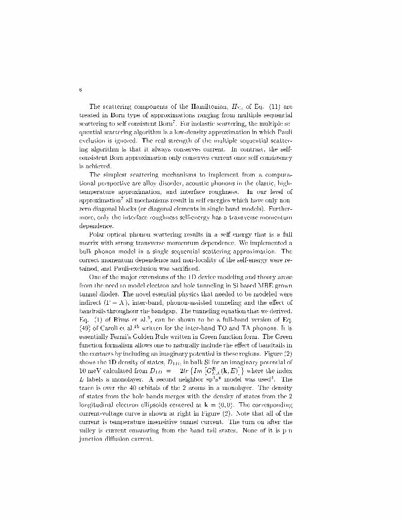
One of the major extensions of the 1D device modeling and theory arose
from the need to model electron and hole tunneling in Si based MBE grown
tunnel diodes. The novel essential physics that needed to be modeled were
indirect (� � X), inter-band, phonon-assisted tunneling and the e�ect of
bandtails throughout the bandgap. The tunneling equation that we derived,
Eq. (1) of Rivas et al.3, can be shown to be a full-band version of Eq.
(49) of Caroli et al.15 written for the inter-band TO and TA phonons. It is
essentially Fermi's Golden Rule written in Green function form. The Green
function formalism allows one to naturally include the e�ect of bandtails in
the contacts by including an imaginary potential in these regions. Figure (2)
shows the 1D density of states, D1D, in bulk Si for an imaginary potential of
10 meV calculated from D1D = �2tr�Im
�GRL;L(k; E)
�where the index
L labels a monolayer. A second neighbor sp3s* model was used3. The
trace is over the 40 orbitals of the 2 atoms in a monolayer. The density
of states from the hole bands merges with the density of states from the 2
longitudinal electron ellipsoids centered at k = (0; 0). The corresponding
current-voltage curve is shown at right in Figure (2). Note that all of the
current is temperature insensitive tunnel current. The turn on after the
valley is current emanating from the band tail states. None of it is p-n
junction di�usion current.

7
Figure 2. Left: One dimensional density of states calculated at transverse k =(kx; ky) = (0; 0) and at k = 0:82(2�=a)(1; 0). Right: Current voltage curve calculatedfor Si tunnel diode with band tails as shown at left.
3. Two Dimensional Simulators
In 1995, one of the authors (D.J.) created under Texas Instruments' De-
caNano program the �rst 2D NEGF device simulator designed for modeling
ultra-scaled Si MOSFETs. This work has continued at Motorola and has
culminated in a 2D NEGF-based simulator suitable for modeling a wide
variety of Si and III-V FETs and nano-photonic devices.
For 2D, the use of the Dyson equation forG< is essential for generalizing
the RGFA to 2D scattering problems. The resulting RGFA operates on
block matrices spanning the transverse dimensions of the device and is
therefore similar in form to multi-orbital 1D problems. Throughout this
section, bold font will be used to denote block matrices, interior block
matrix elements are denoted by j, and longitudinal sites connecting source
to drain are denoted by index i.
With each increase in dimensionality, the physics that can be explictly
modeled must be balanced against increasing computational scale of the
problem. To improve computational performance, we assume that the self-
energies �R and �< are local and that no net energy transfer occurs dur-
ing scattering processes. As a result, the principal e�ect of our model
is to introduce back-scattering into the transport process. Furthermore,
since the scattering mechanisms in fabricated MOSFETs are complicated
by multiple-valley phonon scattering, amorphous-crystalline interfaces, etc.,
we use an empirically calibrated scattering model to encompass all of these
mechanisms. With these assumptions, �R and the current-conserving �<
8
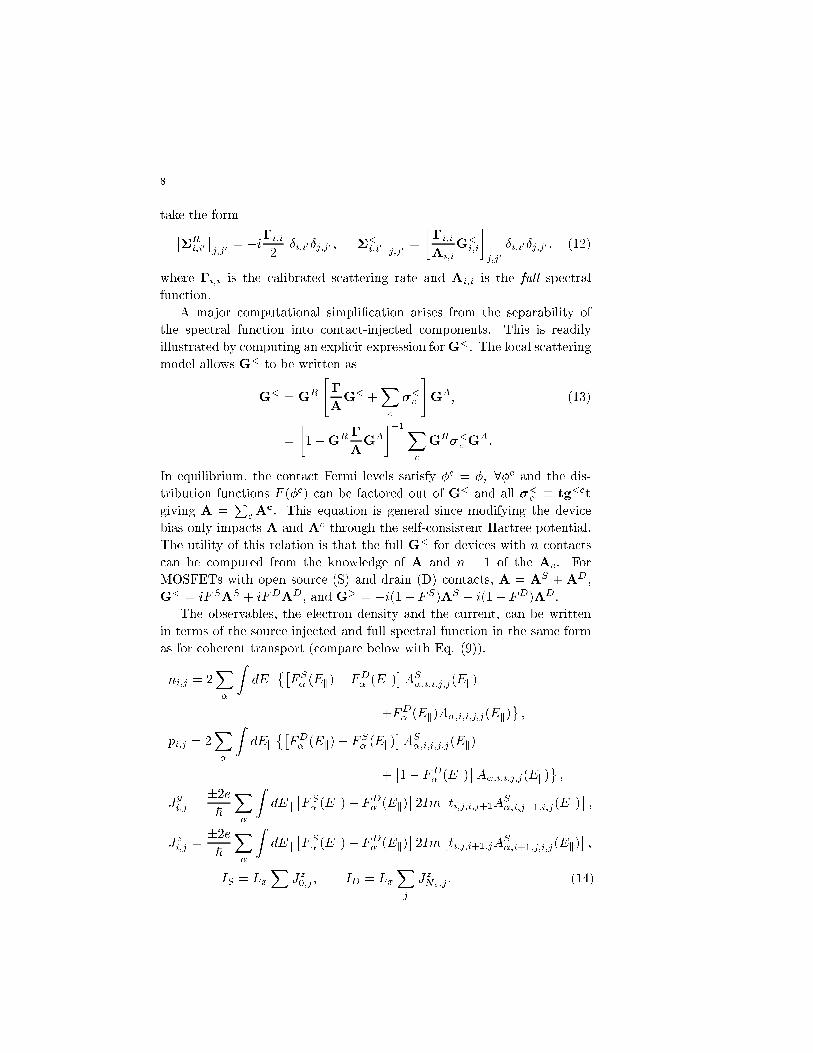
take the form��Ri;i0�j;j0
= �i�i;i
2Æi;i0Æj;j0 ;
��<i;i0�j;j0
=
��i;i
Ai;iG<
i;i
�j;j0
Æi;i0Æj;j0 : (12)
where �i;i is the calibrated scattering rate and Ai;i is the full spectral
function.
A major computational simpli�cation arises from the separability of
the spectral function into contact-injected components. This is readily
illustrated by computing an explicit expression forG<. The local scattering
model allows G< to be written as
G< = GR
"�
AG< +
Xc
�<c
#GA; (13)
=
�1�GR �
AGA
��1Xc
GR�<c G
A:
In equilibrium, the contact Fermi levels satisfy �c = �; 8�c and the dis-
tribution functions F (�c) can be factored out of G< and all �<c � tg<ct
giving A =P
cAc. This equation is general since modifying the device
bias only impacts A and Ac through the self-consistent Hartree potential.
The utility of this relation is that the full G< for devices with n contacts
can be computed from the knowledge of A and n � 1 of the Ac. For
MOSFETs with open source (S) and drain (D) contacts, A = AS +AD ,
G< = iFSAS + iFDAD, and G> = �i(1� FS)AS � i(1� FD)AD.
The observables, the electron density and the current, can be written
in terms of the source injected and full spectral function in the same form
as for coherent transport (compare below with Eq. (9)).
ni;j = 2X�
ZdEk
��FS� (Ek)� FD
� (Ek)�AS�;i;i;j;j(Ek)
+FD� (Ek)A�;i;i;j;j(Ek)
;
pi;j = 2X�
ZdEk
��FD� (Ek)� FS
� (Ek)�AS�;i;i;j;j(Ek)
+�1� FD
� (Ek)�A�;i;i;j;j(Ek)
;
Jyi;j =�2e
~
X�
ZdEk
�FS� (Ek)� FD
� (Ek)�2Im
�ti;j;i;j+1A
S�;i;j+1;i;j(Ek)
�;
Jzi;j =�2e
~
X�
ZdEk
�FS� (Ek)� FD
� (Ek)�2Im
�ti;j;i+1;jA
S�;i+1;j;i;j(Ek)
�;
IS = LxX
Jz0;j ; ID = LxXj
JzNz;j : (14)

9
The signs � and + in the current density expressions refer to electrons and
holes, the index � refers to a particular valley con�guration, and Lx is the
width of the device.
The integration over transverse momentum (kx) is performed analyti-
cally so that the quantities FS=D� in Eq. (14) are given by
FS=D� (Ek) =
�2�2
�m�x��kT
2~2
�1=2
F�1=2
(Ek � �S=D
kT
); (15)
where F�1=2 denotes the Fermi integral of order �1=2.
As usual, the observables require knowledge of the (near) diagonals
of AS and A which provides the incentive for using the RGFA. Our 2D
implementation of the RGFA begins with the surface Green function in the
left (source) at band region which satis�es
gRS =�E�Di;i ��R
i;i � ti;i�1 gRS ti�1;i
��1; (16)
The solution is given by
gRS = t�1h��
p�2 � I
i; � �
�E�D��R
�2t
; (17)
where translational invariance allows the dropping of all longitudinal sub-
scripts. Eq. 17 requires the solution of a general eigenvalue problem for the
sqare-root term and the choice of sign is based on the physical requirement
that the spectral density a � i(gR � gA) be positive de�nite. The surface
g< at the source is then
g<S = iF (�S)aS : (18)
The RGFA for GR is unchanged from Sec. (2) since �R is a known
quantity which is added to the diagonal of H . GR immediately gives A =
i(GR �GRy). The RGFA for AS begins with the Dyson equation for the
left connected g< (cf. Eq. (24) of [7]).
gC<i;i = g<i;i + gRi;iti;i�1gCRi�1;i�1ti�1;ig
C<i;i + gRi;iti;i�1g
C<i�1;i�1ti�1;ig
CAi;i
+ g<i;iti;i�1gCAi�1;i�1ti�1;ig
CAi;i (19)
Upon rearrangement, using g<i;i = gRi;i�Si;ig
Ai;i and gCAi;i = gAi;i +
gAi;iti;i�1gCAi�1;i�1ti�1;ig
CAi;i this becomes
gC<i;i = gCRi;i��Si;i + ti;i�1g
C<i�1;i�1ti�1;i
�gCAi;i (20)
where �Si;i =�i;i
Ai;iG<S
i;i and G<Si;i = iFSAS
i;i.
The superscripts C and B are used as before to indicate whether the
semi-in�nite portion of g<, gR, gA, or aS extends towards the left (source)
10
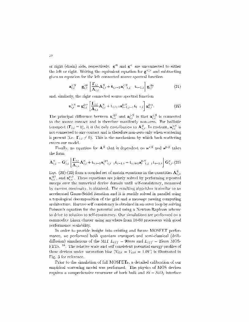
or right (drain) side, respectively. gR and g< are unconnected to either
the left or right. Writing the equivalent equation for gC> and subtracting
gives an equation for the left connected source spectral function
aCSi;i = gCri;i
��i;i
Ai;iASi;i + ti;i�1a
CSi�1;i�1ti�1;i
�gCai;i (21)
and, similarly, the right connected source spectral function
aBSi;i = gBri;i
��i;i
Ai;iASi;i + ti;i+1a
BSi+1;i+1ti+1;i
�gBai;i : (22)
The principal di�erence between aCSi;i and aBSi;i is that aCSi;i is connected
to the source contact and is therefore manifestly non-zero. For ballistic
transport (�i;i � 0), it is the only contribution to ASi;i. In contrast, aBSi;i is
not connected to any contact and is therefore non-zero only when scattering
is present (i.e. �i;i 6= 0). This is the mechanism by which back-scattering
enters our model.
Finally, an equation for AS that is dependent on aCS and aBS takes
the form
ASi;i =Gr
i;i
��i;i
Ai;iASi;i + ti;i�1a
CSi�1;i�1ti�1;i + ti;i+1a
BSi+1;i+1ti+1;i
�Ga
i;i:(23)
Eqs. (21)-(23) form a coupled set of matrix equations in the quantitiesASi;i,
aCSi;i , and aBSi;i . These equations are jointly solved by performing repeated
sweeps over the numerical device domain until self-consistency, measured
by current continuity, is obtained. The resulting algorithm is similar to an
accelerated Gauss-Seidel iteration and it is readily solved in parallel using
a topological decomposition of the grid and a message-passing computing
architecture. Hartree self-consistency is obtained in an outer loop by solving
Poisson's equation for the potential and using a Newton-Raphson scheme
to drive to solution to self-consistency. Our simulations are performed on a
commodity Linux cluster using anywhere from 10-60 processors with good
performance scalability.
In order to provide insight into existing and future MOSFET perfor-
mance, we performed both quantum transport and semi-classical (drift-
di�usion) simulations of the MIT Leff = 90nm and Leff = 25nm MOS-
FETs. 16. The relative scale and self-consistent potential energy pro�les of
these devices under saturation bias (VGS = VDS = 1:0V ) is illustrated in
Fig. 3 for reference.
Prior to the simulation of full MOSFETs, a detailed calibration of our
empirical scattering model was performed. The physics of MOS devices
requires a comprehensive treatment of both bulk and Si � SiO2 interface

11
0-40-80 40 80
0
40
80
Distance (nm)
Dis
tanc
e(n
m)
Potential Energy (eV)
(a)0-40-80 40 80
0
40
80
Distance (nm)
Dis
tanc
e(n
m)
Potential Energy (eV)
(a)
0-40 40
0
40
Distance (nm)
Potential Energy (eV)
Dis
tanc
e(n
m)
(b)
0-40 40
0
40
0-40 40
0
40
Distance (nm)
Potential Energy (eV)
Dis
tanc
e(n
m)
(b)
Figure 3. Self-consistent conduction band (potential energy) pro�les for the (a) Leff =90nm and (b) Leff = 25nm MIT reference MOSFETs.
102
103
0.1 1
Experiment (Takagi)SimulationBD
µ eff(c
m2 /V
s)
Eeff
(MV/cm)
Electron
Hole
Figure 4. Simulated e�ective mobility (�eff ) vs. e�ective �eld (Eeff ) curves generatedfrom the calibrated scattering model
scattering processes so we performed our calibration against experimentally
available e�ective mobility data17. Our mobility model was based on an
explicit linear response calculation of the inversion layer conductivity18 pa-
rameterized with our local scattering model. The results of the calibration,
illustrated in Fig. 4, demonstrate the good agreement achieved between
our model and experimental data.
We subsequently tested our scattering model within our full 2D NEGF
simulator and compared the results against drift-di�usion theory and ex-
perimental data for the 90nm MIT MOSFET16. Although possessing a
short Leff , the 90nm MIT MOSFET has a relatively large SiO2 thickness
(tox = 4:5nm), which minimizes the impact of vertical quantum e�ects

12
0
0.2
0.4
0.6
0.8
-2 -1.5 -1 -0.5 0 0.5 1 1.5 2
ExperimentQuantum TransportDrift-DiffusionBC
I D(m
A/µ
m)
VGS
(V)
(a)
10-12
10-10
10-8
10-6
10-4
-2 -1.5 -1 -0.5 0 0.5 1 1.5 2
I D(A
/µm
)V
GS(V)
(b)
Figure 5. Comparison of (a) linear and (b) log quantum-transport and drift-di�usionsimulated ID-VGS characteristics for the 90nm MIT MOSFET under saturation (VDS =1:0V ). Experimental data for for the nMOS transistor is shown for reference.
(e.g. charge centroid shift) and makes this an essentially semiclassical de-
vice. The results of the comparison (illustrated in Fig. 5) show good
agreement between quantum transport and semiclassical theory, and both
sets of data match well with the available experimental data. This sug-
gests both that quantum-transport simulators can e�ectively simulate re-
alistic device performance and that semi-classical models are still valid for
device technologies on the scale of the 90nm MOSFET. However, future
device scaling is expected to make quantum e�ect more prevalent in device
operating characteristics thereby rendering existing semi-classical models
increasingly invalid. We test out this prediction in the following section.
MOSFET scaling requires the simultaneous reduction in oxide thick-
ness (tox) and gate-length (Lpoly) to achieve sequential improvements in
process technology performance. Presently, devices with tox = 2nm and
Lpoly = 90nm are entering production and devices with signi�cantly smaller
values tox and Lpoly are under development. To gain an understanding of
the degree to which quantum e�ects will in uence future technologies, we
examined two e�ects using our simulator; the quantum-mechanically in-
duced threshold voltage (Vt) shift and the impact sub-threshold tunneling
on device leakage.
A manifestation of any quantum-mechanical system with a step-
boundary or interface (e.g. the Si � SiO2) is that the charge density in
the immediate vicinity of the interface will be depleted because the wave-
function peak is shifted away from the interface. This shift in the induced
charge centroid decreases the e�ective oxide capacitance (Cox) and conse-
quently degrades device performance. For present-day process technologies

13
10-11
10-9
10-7
10-5
10-3
0 0.2 0.4 0.6 0.8 1
Quantum TransportDrift-Diffusion
I D(A
/µm
)
VGS
(V)
(a)
0
0.15
0.3
0.45
0.6
0.2 0.4 0.6 0.8 1
I D(m
A/µ
m)
VGS
(V)
10-11
10-9
10-7
10-5
10-3
-1 -0.8 -0.6 -0.4 -0.2 0
I D(A
/µm
)
VGS
(V)
(b)
0
0.1
0.2
0.3
-1 -0.8 -0.6 -0.4 -0.2
I D(m
A/µ
m)
VGS
(V)
Figure 6. Comparison of quantum-transport and drift-di�usion simulated ID-VGS char-acteristics for the 25nm MIT MOSFET under saturation bias (VDS = 1:0V ). Both (a)nMOS and (b) pMOS transistor data is shown
0
2
4
6
8
10
-0.15 0 0.15 0.3
Leff
=90nm
Leff
=25nm
Tra
nsm
issi
on
Energy (eV)
(a)
0
0.1
0.2
0.3
0.4
0.5
-0.2 -0.1 0 0.1 0.2
Cur
rent
Den
sity
(a.u
.)
Energy (eV)
0
0.3
0.6
0.9
1.2
0.3 0.33 0.36 0.39 0.42
Leff
=90nm
Leff
=25nm
Nor
mal
ized
Cur
rent
Den
sity
(arb
.uni
ts)
Energy (eV)
(b)
10-3
10-2
10-1
100
0.25 0.3 0.35 0.4
Figure 7. Comparison of (a) saturation transmission characteristics and (b) normalizedcurrent density for the Leff = 90nm and Leff = 25nm MIT MOSFETs
with tox < 2:5nm, the capacitive loading of the centroid shift can be signif-
icant. The e�ect is illustrated in Fig. 6 which compares quantum transport
and semiclassical simulations of the 25nm MIT MOSFET (tox = 1:5nm).
The overall impact is a predicted 0:2V (0:1) nMOS (pMOS) Vt shift from
the semiclassical model data. Clearly, the incorporation of this e�ect in
semiclassical device simulators is vital to their continued use in technol-
ogy simulation and e�orts are already underway to augment semiclassical
models with e�ective quantum potentials. 19.
An additional issue a�ecting scaled MOSFETs is onset of tunneling
through the channel barrier when the device is biased in the o�-state

14
Figure 8. Transmission and density of states for (left) one of the 4 transverse X valleysand (right) one of the longitudinal X valleys.
(VGS = 0V; VDS = VDD). This is a mechanism that can be generally
ignored for contemporary technologies with LG > 75nm but which may
become signi�cant in future scaled devices. To assess it's potential impact,
the transmission characteristics and current density for the 90nm and 25nm
MOSFETs are compared in Fig. 7.
As carriers ow through a MOSFET, their con�nement to subbands by
the gate-induced potential leads to steps in transmission spectrum (Fig.
7(a)) corresponding to the onset of subband conduction. In the o�-state,
a source-drain potential barrier is designed to be an impediment to car-
rier transport thereby allowing the MOSFET to switch o�. However, as
illustrated in Fig. 7(b), the 25nm devices can have a substantial current-
density tail which indicates the presence of tunneling through the source
barrier. For the 25nm device, the sub-threshold tail accounts for about 50
% of the o�-state current, and this component can be expected to increase
exponentially as device technologies scale further.
4. Three Dimensional Simulators
We have been modeling 3D Si nanopillar structures and are particularly
interested in ultra-narrow pillar and quantum dot structures with large
quantum con�nement. We started with a discretized single band model.
Example calculations are shown in Figure (8) of a 2nm diameter Si pillar.
The left plot shows the density of states and transmission for one of the 4
transverse X valleys. These valleys have their long axis perpendicular to the
length of the cylinder. The right plot is for one of the longitudinal X valleys
which has the long axis parallel to the length of the cylinder. The density of

15
Figure 9. Density of states for same cylinder as in Fig. 8 calculated with sp3s�d5 model.It is strongly a�ected by dangling bonds at the surface of the cylinder.
states is calculated from �2Im tr fGx;y;x;y(E)g where the trace is over all
sites in a plane of the cylinder. The minimum quantization energies are 400
meV for the transverse valleys and 650 meV for the longitudinal valleys.
These single band calculations overestimate the quantization energy in the
ultimate quantum limit. Full-band models accurate near the X point are
required.
We have recently begun working on a full band sp3s�d5 model. A prelim-
inary calculation of the same pillar is shown in Figure (9). There appears to
be a large density of states originating from dangling bonds at the surface
of the cylinder. This work is in its initial stages. The most cpu intensive
part of this calculation is the calculation of the surface Green functions for
the open system boundary conditions. At this time we are simply iterating
Eq. (3) to convergence. From our experience with 1D, this is the slowest
method for calculating the surface Green function.
In conclusion, we have found the NEGF approach to be extremely suc-
cessful for modeling quantum semiconductor devices. It has allowed for
much creativity and exibility in treating the traditionally diÆcult prob-
lems in quantum device simulation, the open contacts and incoherent scat-
tering from phonons and disorder.
Acknowledgments
This work has been supported at various times by Texas Instruments,
Raytheon, Motorola, DARPA/AFOSR, and the NSF. R.L. wishes to ac-
knowledge that within this compendium describing work in 1D, 2D, and
3D, credit for the 2D work belongs solely to D.J.

References
1. D. Jovanovic and R. Venugopal. In 7th International Workshop on Compu-
tational Electronics. Book of Abstracts, page 30, Glasgow, 2000. IWCE.2. A. Svizhenko, M. P. Anantram, T. R. Govindan, B. Biegel, and R. Venugopal.
J. Appl. Phys., 91(4):2343{2354, 2002.3. C. Rivas, R. Lake, G. Klimech, W. R. Frensley, M. V. Fischetti, P. E. Thomp-
son, S. L. Rommel, and P. R. Berger. Appl. Phys. Lett., 78(6):814{6, 2001.4. R. Lake. In 2001 IEDM Technical Digest, pages 5.5.1 { 5.5.4, New York,
2001. IEEE.5. M. P. Anantram. Appl. Phys. Lett., 78(20):2005{7, 2001.6. P. S. Damle, A. W. Ghosh, and S. Datta. Phys. Rev. B, 64(20):201403, 2001.7. R. Lake, G. Klimeck, R. C. Bowen, and D. Jovanovic. J. Appl. Phys.,
81(12):7845{7869, 1997.8. R. Lake and S. Datta. Phys. Rev. B, 46(8):4757{4763, 1992.9. S. Hersh�eld, J. H. Davies, and J. W. Wilkins, Phys. Rev. B, 46, 7046 (1992);
Y. Meir and N. S. Wingreen, Phys. Rev. Lett., 68, 2512 (1992).10. D. K. Blanks, G. Klimeck, R. Lake, D. Jovanovic, R. C. Bowen, C. Fer-
nando, W. R. Frensley, and M. Leng. In Compound Semiconductors 1997.
Proceedings of the IEEE Twenty-Fourth International Symposium on Com-
pound Semiconductors, pages 639{642, New York, 1998. IEEE.11. We believe that a similar graphic was originally created by G. Klimeck during
the NEMO program.12. Timothy B. Boykin. Phys. Rev. B, 54:8107, 1996.13. G. Klimeck, R. Lake, R. C. Bowen, W. R. Frensley, and T. Moise. Appl.
Phys. Lett., 67(17):2539{2541, 1995.14. R. Lake, G. Klimeck, R. Bowen, D. Jovanovic, P. Sotirelis, and W. R. Frens-
ley. VLSI Design, 6:9, 1998.15. C. Caroli, R. Combescot, P. Nozieres, and D. Saint-James. J. Phys. C: Solid
State Physics, 5:21{42, 1972.16. D. A. Antoniadis, I. J. Djomehri, K. M. Jackson, and S. Miller, \http://www-
mtl.mit.edu:80/Well/" , 2001.17. S. Takagi, A. Toriumi, M. Iwase, H. Tango, IEEE Trans. Electron Devices
41; 2357 (1994).18. D. Vasileska and D. Ferry, IEEE Trans. Electron Devices 44, 577-583 (1997).19. R. Akis, L. Shifren, D. K. Ferry, and D. Vasileska, Physica Status Solidi B
226, 1 (2001).
16
Index 17
IndexG<, 7
�<, 7�R, 71D, 2, 4, 62D, 2, 43D, 2, 14
AlAs, 1alloy disorder, 2, 5, 6
ballistic transport, 10bandstructure
full, 1, 2, 15sp3s�d5, 2, 15sp3s*, 6
bandtails, 1, 6basis, 5Born, 2, 5, 6
self-consistent, 6boundaries
open, 3, 5open-system, 1
Caroli, 6contact, 2, 5, 8correlation, 5crystal potential, 5current, 4, 8, 14
coherent, 4continuity, 10
density of states, 6, 15device, 2drain, 2, 7, 14drift-di�usion, 11Dyson equation, 7
electron density, 4, 8energy broadening, 5energy transport, 2exchange, 5
Fermi
Golden Rule, 6
gate, 2Green function
G<, 4, 8
retarded, 3surface, 3, 4, 15
Hartree, 2, 5, 8, 10heat transport, 2HEMT, 1holes, 9
imaginary potential, 3, 5, 6In0:47Ga0:53As, 1In0:52Al0:48As, 1InAs, 1incoherent scattering, 2, 3interface roughness, 2, 5, 6ionized impurity, 5iteration, 3
kinetic energy, 5
leads, 3Linux, 10local density approximation, 2, 5
matrix, 10block, 2full, 4tridiagonal, 3
MBE, 6mobility, 11MOSFET, 1, 10, 13
MIT, 11Motorola, 7
NEMO, 2, 4Newton-Raphson, 10
p-n junction, 6parallel computing, 2, 10

18 Index
phononacoustic, 5, 6polar-optical, 4, 5
planar-orbital, 5Poisson's equation, 5, 10
quantum dot, 14
recursive Green function algorithm,3, 4, 7, 9G<, 4
RGFA see recursive Green functionalgorithm, 3
RTD, 1
scattering, 5, 10interface, 11multiple-sequential, 6phonon, 2
self-consistency, 10self-consistent, 5self-energy, 5{7Si, 1, 6, 14SixGe1�x, 1single band, 2, 14source, 2, 7, 14spectral function, 8, 10
Texas Instruments, 2threshold voltage, 12tunnel diode, 1, 2, 6tunneling, 13
indirect, 6inter-band, 2, 6inter-valley, 2phonon-assisted, 2, 6sub-threshold, 12