Nios II Processor Reference Handbook - University … · 101 Innovation Drive San Jose, CA 95134 ...
260
101 Innovation Drive San Jose, CA 95134 www.altera.com Nios II Processor Reference Handbook NII5V1-9.0
Transcript of Nios II Processor Reference Handbook - University … · 101 Innovation Drive San Jose, CA 95134 ...
101 Innovation Drive San Jose, CA 95134 www.altera.com
Nios II Processor Reference Handbook
NII5V1-9.0

Copyright © 2009 Altera Corporation. All rights reserved. Altera, The Programmable Solutions Company, the stylized Altera logo, specific device designations, and all other words and logos that are identified as trademarks and/or service marks are, unless noted otherwise, the trademarks and service marks of Altera Corporation in the U.S. and other countries. All other product or service names are the property of their respective holders. Altera products are protected under numerous U.S. and foreign patents and pending ap-plications, maskwork rights, and copyrights. Altera warrants performance of its semiconductor products to current specifications in accordance with Altera's standard warranty, but reserves the right to make changes to any products and services at any time without notice. Altera assumes no responsibility or liability arising out of the application or use of any information, product, or service described herein except as expressly agreed to in writing by Altera Corporation. Altera customers are advised to obtain the latest version of device specifications before relying on any published information and before placing orders for products or services.
© March 2009 Altera Corporation
Contents
Chapter Revision Dates . . . . . . . . . . . . . . . . . . . . . . . . . . . . . . . . . . . . . . . . . . . . . . . . . . . . . . . . . . . . . . . . . . . . . . ix
List of Figures . . . . . . . . . . . . . . . . . . . . . . . . . . . . . . . . . . . . . . . . . . . . . . . . . . . . . . . . . . . . . . . . . . . . . . . . . . . . . . xi
List of Tables . . . . . . . . . . . . . . . . . . . . . . . . . . . . . . . . . . . . . . . . . . . . . . . . . . . . . . . . . . . . . . . . . . . . . . . . . . . . . . xiii
Section I. Nios II Processor Design
Chapter 1. IntroductionIntroduction . . . . . . . . . . . . . . . . . . . . . . . . . . . . . . . . . . . . . . . . . . . . . . . . . . . . . . . . . . . . . . . . . . . . . . . . . . . . 1–1Nios II Processor System Basics . . . . . . . . . . . . . . . . . . . . . . . . . . . . . . . . . . . . . . . . . . . . . . . . . . . . . . . . . . . 1–1Getting Started with the Nios II Processor . . . . . . . . . . . . . . . . . . . . . . . . . . . . . . . . . . . . . . . . . . . . . . . . . . 1–2Customizing Nios II Processor Designs . . . . . . . . . . . . . . . . . . . . . . . . . . . . . . . . . . . . . . . . . . . . . . . . . . . . . 1–3Configurable Soft-Core Processor Concepts . . . . . . . . . . . . . . . . . . . . . . . . . . . . . . . . . . . . . . . . . . . . . . . . . 1–4
Configurable Soft-Core Processor . . . . . . . . . . . . . . . . . . . . . . . . . . . . . . . . . . . . . . . . . . . . . . . . . . . . . . . 1–4Flexible Peripheral Set and Address Map . . . . . . . . . . . . . . . . . . . . . . . . . . . . . . . . . . . . . . . . . . . . . . . . . 1–4
Standard Peripherals . . . . . . . . . . . . . . . . . . . . . . . . . . . . . . . . . . . . . . . . . . . . . . . . . . . . . . . . . . . . . . . . 1–4Custom Peripherals . . . . . . . . . . . . . . . . . . . . . . . . . . . . . . . . . . . . . . . . . . . . . . . . . . . . . . . . . . . . . . . . . 1–5Custom Instructions . . . . . . . . . . . . . . . . . . . . . . . . . . . . . . . . . . . . . . . . . . . . . . . . . . . . . . . . . . . . . . . . 1–5
Automated System Generation . . . . . . . . . . . . . . . . . . . . . . . . . . . . . . . . . . . . . . . . . . . . . . . . . . . . . . . . . 1–5OpenCore Plus Evaluation . . . . . . . . . . . . . . . . . . . . . . . . . . . . . . . . . . . . . . . . . . . . . . . . . . . . . . . . . . . . . . . . 1–5Referenced Documents . . . . . . . . . . . . . . . . . . . . . . . . . . . . . . . . . . . . . . . . . . . . . . . . . . . . . . . . . . . . . . . . . . . 1–6Document Revision History . . . . . . . . . . . . . . . . . . . . . . . . . . . . . . . . . . . . . . . . . . . . . . . . . . . . . . . . . . . . . . 1–6
Chapter 2. Processor ArchitectureIntroduction . . . . . . . . . . . . . . . . . . . . . . . . . . . . . . . . . . . . . . . . . . . . . . . . . . . . . . . . . . . . . . . . . . . . . . . . . . . . 2–1Processor Implementation . . . . . . . . . . . . . . . . . . . . . . . . . . . . . . . . . . . . . . . . . . . . . . . . . . . . . . . . . . . . . . . . 2–3Register File . . . . . . . . . . . . . . . . . . . . . . . . . . . . . . . . . . . . . . . . . . . . . . . . . . . . . . . . . . . . . . . . . . . . . . . . . . . . 2–3Arithmetic Logic Unit . . . . . . . . . . . . . . . . . . . . . . . . . . . . . . . . . . . . . . . . . . . . . . . . . . . . . . . . . . . . . . . . . . . . 2–3
Unimplemented Instructions . . . . . . . . . . . . . . . . . . . . . . . . . . . . . . . . . . . . . . . . . . . . . . . . . . . . . . . . . . . 2–4Custom Instructions . . . . . . . . . . . . . . . . . . . . . . . . . . . . . . . . . . . . . . . . . . . . . . . . . . . . . . . . . . . . . . . . . . . 2–4Floating-Point Instructions . . . . . . . . . . . . . . . . . . . . . . . . . . . . . . . . . . . . . . . . . . . . . . . . . . . . . . . . . . . . . 2–4
Software Development Considerations . . . . . . . . . . . . . . . . . . . . . . . . . . . . . . . . . . . . . . . . . . . . . . . . 2–6Reset and Debug Signals . . . . . . . . . . . . . . . . . . . . . . . . . . . . . . . . . . . . . . . . . . . . . . . . . . . . . . . . . . . . . . . . . 2–7Exception and Interrupt Controller . . . . . . . . . . . . . . . . . . . . . . . . . . . . . . . . . . . . . . . . . . . . . . . . . . . . . . . . 2–7
Exception Controller . . . . . . . . . . . . . . . . . . . . . . . . . . . . . . . . . . . . . . . . . . . . . . . . . . . . . . . . . . . . . . . . . . 2–7Integral Interrupt Controller . . . . . . . . . . . . . . . . . . . . . . . . . . . . . . . . . . . . . . . . . . . . . . . . . . . . . . . . . . . . 2–8Interrupt Vector Custom Instruction . . . . . . . . . . . . . . . . . . . . . . . . . . . . . . . . . . . . . . . . . . . . . . . . . . . . . 2–8
Memory and I/O Organization . . . . . . . . . . . . . . . . . . . . . . . . . . . . . . . . . . . . . . . . . . . . . . . . . . . . . . . . . . . . 2–9Instruction and Data Buses . . . . . . . . . . . . . . . . . . . . . . . . . . . . . . . . . . . . . . . . . . . . . . . . . . . . . . . . . . . . 2–10
Memory and Peripheral Access . . . . . . . . . . . . . . . . . . . . . . . . . . . . . . . . . . . . . . . . . . . . . . . . . . . . . . 2–11Instruction Master Port . . . . . . . . . . . . . . . . . . . . . . . . . . . . . . . . . . . . . . . . . . . . . . . . . . . . . . . . . . . . . 2–11Data Master Port . . . . . . . . . . . . . . . . . . . . . . . . . . . . . . . . . . . . . . . . . . . . . . . . . . . . . . . . . . . . . . . . . . 2–11Shared Memory for Instructions and Data . . . . . . . . . . . . . . . . . . . . . . . . . . . . . . . . . . . . . . . . . . . . 2–12
Cache Memory . . . . . . . . . . . . . . . . . . . . . . . . . . . . . . . . . . . . . . . . . . . . . . . . . . . . . . . . . . . . . . . . . . . . . . 2–12Configurable Cache Memory Options . . . . . . . . . . . . . . . . . . . . . . . . . . . . . . . . . . . . . . . . . . . . . . . . 2–12Effective Use of Cache Memory . . . . . . . . . . . . . . . . . . . . . . . . . . . . . . . . . . . . . . . . . . . . . . . . . . . . . . 2–12Cache Bypass Methods . . . . . . . . . . . . . . . . . . . . . . . . . . . . . . . . . . . . . . . . . . . . . . . . . . . . . . . . . . . . . 2–13
Nios II Processor Reference HandbookPreliminary
iv Contents
Tightly-Coupled Memory . . . . . . . . . . . . . . . . . . . . . . . . . . . . . . . . . . . . . . . . . . . . . . . . . . . . . . . . . . . . . 2–13Accessing Tightly-Coupled Memory . . . . . . . . . . . . . . . . . . . . . . . . . . . . . . . . . . . . . . . . . . . . . . . . . 2–14Effective Use of Tightly-Coupled Memory . . . . . . . . . . . . . . . . . . . . . . . . . . . . . . . . . . . . . . . . . . . . 2–14
Address Map . . . . . . . . . . . . . . . . . . . . . . . . . . . . . . . . . . . . . . . . . . . . . . . . . . . . . . . . . . . . . . . . . . . . . . . . 2–14Memory Management Unit . . . . . . . . . . . . . . . . . . . . . . . . . . . . . . . . . . . . . . . . . . . . . . . . . . . . . . . . . . . . 2–14Memory Protection Unit . . . . . . . . . . . . . . . . . . . . . . . . . . . . . . . . . . . . . . . . . . . . . . . . . . . . . . . . . . . . . . 2–15
JTAG Debug Module . . . . . . . . . . . . . . . . . . . . . . . . . . . . . . . . . . . . . . . . . . . . . . . . . . . . . . . . . . . . . . . . . . . 2–16JTAG Target Connection . . . . . . . . . . . . . . . . . . . . . . . . . . . . . . . . . . . . . . . . . . . . . . . . . . . . . . . . . . . . . . 2–17Download and Execute Software . . . . . . . . . . . . . . . . . . . . . . . . . . . . . . . . . . . . . . . . . . . . . . . . . . . . . . . 2–17Software Breakpoints . . . . . . . . . . . . . . . . . . . . . . . . . . . . . . . . . . . . . . . . . . . . . . . . . . . . . . . . . . . . . . . . . 2–17Hardware Breakpoints . . . . . . . . . . . . . . . . . . . . . . . . . . . . . . . . . . . . . . . . . . . . . . . . . . . . . . . . . . . . . . . . 2–17Hardware Triggers . . . . . . . . . . . . . . . . . . . . . . . . . . . . . . . . . . . . . . . . . . . . . . . . . . . . . . . . . . . . . . . . . . . 2–17
Armed Triggers . . . . . . . . . . . . . . . . . . . . . . . . . . . . . . . . . . . . . . . . . . . . . . . . . . . . . . . . . . . . . . . . . . . 2–18Triggering on Ranges of Values . . . . . . . . . . . . . . . . . . . . . . . . . . . . . . . . . . . . . . . . . . . . . . . . . . . . . 2–18
Trace Capture . . . . . . . . . . . . . . . . . . . . . . . . . . . . . . . . . . . . . . . . . . . . . . . . . . . . . . . . . . . . . . . . . . . . . . . 2–18Execution vs. Data Trace . . . . . . . . . . . . . . . . . . . . . . . . . . . . . . . . . . . . . . . . . . . . . . . . . . . . . . . . . . . . 2–19Trace Frames . . . . . . . . . . . . . . . . . . . . . . . . . . . . . . . . . . . . . . . . . . . . . . . . . . . . . . . . . . . . . . . . . . . . . . 2–19
Referenced Documents . . . . . . . . . . . . . . . . . . . . . . . . . . . . . . . . . . . . . . . . . . . . . . . . . . . . . . . . . . . . . . . . . . 2–20Document Revision History . . . . . . . . . . . . . . . . . . . . . . . . . . . . . . . . . . . . . . . . . . . . . . . . . . . . . . . . . . . . . 2–20
Chapter 3. Programming ModelIntroduction . . . . . . . . . . . . . . . . . . . . . . . . . . . . . . . . . . . . . . . . . . . . . . . . . . . . . . . . . . . . . . . . . . . . . . . . . . . . 3–1Operating Modes . . . . . . . . . . . . . . . . . . . . . . . . . . . . . . . . . . . . . . . . . . . . . . . . . . . . . . . . . . . . . . . . . . . . . . . . 3–2
Supervisor Mode . . . . . . . . . . . . . . . . . . . . . . . . . . . . . . . . . . . . . . . . . . . . . . . . . . . . . . . . . . . . . . . . . . . . . 3–2User Mode . . . . . . . . . . . . . . . . . . . . . . . . . . . . . . . . . . . . . . . . . . . . . . . . . . . . . . . . . . . . . . . . . . . . . . . . . . . 3–2
Memory Management Unit . . . . . . . . . . . . . . . . . . . . . . . . . . . . . . . . . . . . . . . . . . . . . . . . . . . . . . . . . . . . . . . 3–3Recommended Usage . . . . . . . . . . . . . . . . . . . . . . . . . . . . . . . . . . . . . . . . . . . . . . . . . . . . . . . . . . . . . . . . . 3–3Memory Management . . . . . . . . . . . . . . . . . . . . . . . . . . . . . . . . . . . . . . . . . . . . . . . . . . . . . . . . . . . . . . . . . 3–3
Virtual Addressing . . . . . . . . . . . . . . . . . . . . . . . . . . . . . . . . . . . . . . . . . . . . . . . . . . . . . . . . . . . . . . . . . 3–3Memory Protection . . . . . . . . . . . . . . . . . . . . . . . . . . . . . . . . . . . . . . . . . . . . . . . . . . . . . . . . . . . . . . . . . 3–4
Address Space and Memory Partitions . . . . . . . . . . . . . . . . . . . . . . . . . . . . . . . . . . . . . . . . . . . . . . . . . . . 3–4Virtual Memory Address Space . . . . . . . . . . . . . . . . . . . . . . . . . . . . . . . . . . . . . . . . . . . . . . . . . . . . . . 3–4Physical Memory Address Space . . . . . . . . . . . . . . . . . . . . . . . . . . . . . . . . . . . . . . . . . . . . . . . . . . . . . 3–5Data Cacheability . . . . . . . . . . . . . . . . . . . . . . . . . . . . . . . . . . . . . . . . . . . . . . . . . . . . . . . . . . . . . . . . . . . 3–6
TLB Organization . . . . . . . . . . . . . . . . . . . . . . . . . . . . . . . . . . . . . . . . . . . . . . . . . . . . . . . . . . . . . . . . . . . . . 3–6TLB Lookups . . . . . . . . . . . . . . . . . . . . . . . . . . . . . . . . . . . . . . . . . . . . . . . . . . . . . . . . . . . . . . . . . . . . . . . . . 3–7
Memory Protection Unit . . . . . . . . . . . . . . . . . . . . . . . . . . . . . . . . . . . . . . . . . . . . . . . . . . . . . . . . . . . . . . . . . . 3–8Memory Regions . . . . . . . . . . . . . . . . . . . . . . . . . . . . . . . . . . . . . . . . . . . . . . . . . . . . . . . . . . . . . . . . . . . . . . 3–8
Base Address . . . . . . . . . . . . . . . . . . . . . . . . . . . . . . . . . . . . . . . . . . . . . . . . . . . . . . . . . . . . . . . . . . . . . . 3–8Region Type . . . . . . . . . . . . . . . . . . . . . . . . . . . . . . . . . . . . . . . . . . . . . . . . . . . . . . . . . . . . . . . . . . . . . . . 3–9Region Index . . . . . . . . . . . . . . . . . . . . . . . . . . . . . . . . . . . . . . . . . . . . . . . . . . . . . . . . . . . . . . . . . . . . . . . 3–9Region Size or Upper Address Limit . . . . . . . . . . . . . . . . . . . . . . . . . . . . . . . . . . . . . . . . . . . . . . . . . . 3–9Access Permissions . . . . . . . . . . . . . . . . . . . . . . . . . . . . . . . . . . . . . . . . . . . . . . . . . . . . . . . . . . . . . . . . . 3–9Default Cacheability . . . . . . . . . . . . . . . . . . . . . . . . . . . . . . . . . . . . . . . . . . . . . . . . . . . . . . . . . . . . . . . . 3–9
Overlapping Regions . . . . . . . . . . . . . . . . . . . . . . . . . . . . . . . . . . . . . . . . . . . . . . . . . . . . . . . . . . . . . . . . . 3–10Enabling the MPU . . . . . . . . . . . . . . . . . . . . . . . . . . . . . . . . . . . . . . . . . . . . . . . . . . . . . . . . . . . . . . . . . . . 3–10
General-Purpose Registers . . . . . . . . . . . . . . . . . . . . . . . . . . . . . . . . . . . . . . . . . . . . . . . . . . . . . . . . . . . . . . . 3–10Control Registers . . . . . . . . . . . . . . . . . . . . . . . . . . . . . . . . . . . . . . . . . . . . . . . . . . . . . . . . . . . . . . . . . . . . . . . 3–11
The status Register . . . . . . . . . . . . . . . . . . . . . . . . . . . . . . . . . . . . . . . . . . . . . . . . . . . . . . . . . . . . . . . . . . . 3–12The estatus Register . . . . . . . . . . . . . . . . . . . . . . . . . . . . . . . . . . . . . . . . . . . . . . . . . . . . . . . . . . . . . . . . . . 3–12The bstatus Register . . . . . . . . . . . . . . . . . . . . . . . . . . . . . . . . . . . . . . . . . . . . . . . . . . . . . . . . . . . . . . . . . . 3–13The ienable Register . . . . . . . . . . . . . . . . . . . . . . . . . . . . . . . . . . . . . . . . . . . . . . . . . . . . . . . . . . . . . . . . . . 3–13The ipending Register . . . . . . . . . . . . . . . . . . . . . . . . . . . . . . . . . . . . . . . . . . . . . . . . . . . . . . . . . . . . . . . . 3–13The cpuid Register . . . . . . . . . . . . . . . . . . . . . . . . . . . . . . . . . . . . . . . . . . . . . . . . . . . . . . . . . . . . . . . . . . . 3–13
Nios II Processor Reference Handbook © March 2009 Altera CorporationPreliminary
Contents v
The exception Register . . . . . . . . . . . . . . . . . . . . . . . . . . . . . . . . . . . . . . . . . . . . . . . . . . . . . . . . . . . . . . . . 3–13The pteaddr Register . . . . . . . . . . . . . . . . . . . . . . . . . . . . . . . . . . . . . . . . . . . . . . . . . . . . . . . . . . . . . . . . . 3–14The tlbacc Register . . . . . . . . . . . . . . . . . . . . . . . . . . . . . . . . . . . . . . . . . . . . . . . . . . . . . . . . . . . . . . . . . . . 3–14The tlbmisc Register . . . . . . . . . . . . . . . . . . . . . . . . . . . . . . . . . . . . . . . . . . . . . . . . . . . . . . . . . . . . . . . . . . 3–15
The RD Flag . . . . . . . . . . . . . . . . . . . . . . . . . . . . . . . . . . . . . . . . . . . . . . . . . . . . . . . . . . . . . . . . . . . . . . 3–16The WE Flag . . . . . . . . . . . . . . . . . . . . . . . . . . . . . . . . . . . . . . . . . . . . . . . . . . . . . . . . . . . . . . . . . . . . . . 3–17The WAY Field . . . . . . . . . . . . . . . . . . . . . . . . . . . . . . . . . . . . . . . . . . . . . . . . . . . . . . . . . . . . . . . . . . . . 3–17The PID Field . . . . . . . . . . . . . . . . . . . . . . . . . . . . . . . . . . . . . . . . . . . . . . . . . . . . . . . . . . . . . . . . . . . . . 3–17The DBL Flag . . . . . . . . . . . . . . . . . . . . . . . . . . . . . . . . . . . . . . . . . . . . . . . . . . . . . . . . . . . . . . . . . . . . . 3–17The BAD Flag . . . . . . . . . . . . . . . . . . . . . . . . . . . . . . . . . . . . . . . . . . . . . . . . . . . . . . . . . . . . . . . . . . . . . 3–18The PERM Flag . . . . . . . . . . . . . . . . . . . . . . . . . . . . . . . . . . . . . . . . . . . . . . . . . . . . . . . . . . . . . . . . . . . . 3–18The D Flag . . . . . . . . . . . . . . . . . . . . . . . . . . . . . . . . . . . . . . . . . . . . . . . . . . . . . . . . . . . . . . . . . . . . . . . . 3–18
The badaddr Register . . . . . . . . . . . . . . . . . . . . . . . . . . . . . . . . . . . . . . . . . . . . . . . . . . . . . . . . . . . . . . . . . 3–18The config Register . . . . . . . . . . . . . . . . . . . . . . . . . . . . . . . . . . . . . . . . . . . . . . . . . . . . . . . . . . . . . . . . . . . 3–19The mpubase Register . . . . . . . . . . . . . . . . . . . . . . . . . . . . . . . . . . . . . . . . . . . . . . . . . . . . . . . . . . . . . . . . 3–19The mpuacc Register . . . . . . . . . . . . . . . . . . . . . . . . . . . . . . . . . . . . . . . . . . . . . . . . . . . . . . . . . . . . . . . . . 3–20
The MASK Field . . . . . . . . . . . . . . . . . . . . . . . . . . . . . . . . . . . . . . . . . . . . . . . . . . . . . . . . . . . . . . . . . . . 3–21The LIMIT Field . . . . . . . . . . . . . . . . . . . . . . . . . . . . . . . . . . . . . . . . . . . . . . . . . . . . . . . . . . . . . . . . . . . 3–22The C Flag . . . . . . . . . . . . . . . . . . . . . . . . . . . . . . . . . . . . . . . . . . . . . . . . . . . . . . . . . . . . . . . . . . . . . . . . 3–23The PERM Field . . . . . . . . . . . . . . . . . . . . . . . . . . . . . . . . . . . . . . . . . . . . . . . . . . . . . . . . . . . . . . . . . . . 3–23The RD Flag . . . . . . . . . . . . . . . . . . . . . . . . . . . . . . . . . . . . . . . . . . . . . . . . . . . . . . . . . . . . . . . . . . . . . . 3–23The WR Flag . . . . . . . . . . . . . . . . . . . . . . . . . . . . . . . . . . . . . . . . . . . . . . . . . . . . . . . . . . . . . . . . . . . . . . 3–23
Working with the MPU . . . . . . . . . . . . . . . . . . . . . . . . . . . . . . . . . . . . . . . . . . . . . . . . . . . . . . . . . . . . . . . . . 3–24MPU Region Read and Write Operations . . . . . . . . . . . . . . . . . . . . . . . . . . . . . . . . . . . . . . . . . . . . . . . . 3–24MPU Initialization . . . . . . . . . . . . . . . . . . . . . . . . . . . . . . . . . . . . . . . . . . . . . . . . . . . . . . . . . . . . . . . . . . . 3–25Debugger Access . . . . . . . . . . . . . . . . . . . . . . . . . . . . . . . . . . . . . . . . . . . . . . . . . . . . . . . . . . . . . . . . . . . . . 3–25
Exception Processing . . . . . . . . . . . . . . . . . . . . . . . . . . . . . . . . . . . . . . . . . . . . . . . . . . . . . . . . . . . . . . . . . . . 3–25Reset Exceptions . . . . . . . . . . . . . . . . . . . . . . . . . . . . . . . . . . . . . . . . . . . . . . . . . . . . . . . . . . . . . . . . . . . . . 3–27Break Exceptions . . . . . . . . . . . . . . . . . . . . . . . . . . . . . . . . . . . . . . . . . . . . . . . . . . . . . . . . . . . . . . . . . . . . . 3–28
Processing a Break . . . . . . . . . . . . . . . . . . . . . . . . . . . . . . . . . . . . . . . . . . . . . . . . . . . . . . . . . . . . . . . . . 3–28Register Usage . . . . . . . . . . . . . . . . . . . . . . . . . . . . . . . . . . . . . . . . . . . . . . . . . . . . . . . . . . . . . . . . . . . . 3–28Returning From a Break . . . . . . . . . . . . . . . . . . . . . . . . . . . . . . . . . . . . . . . . . . . . . . . . . . . . . . . . . . . . 3–29
Interrupt Exceptions . . . . . . . . . . . . . . . . . . . . . . . . . . . . . . . . . . . . . . . . . . . . . . . . . . . . . . . . . . . . . . . . . . 3–29Instruction-Related Exceptions . . . . . . . . . . . . . . . . . . . . . . . . . . . . . . . . . . . . . . . . . . . . . . . . . . . . . . . . . 3–30
Trap Instruction . . . . . . . . . . . . . . . . . . . . . . . . . . . . . . . . . . . . . . . . . . . . . . . . . . . . . . . . . . . . . . . . . . . 3–31Break Instruction . . . . . . . . . . . . . . . . . . . . . . . . . . . . . . . . . . . . . . . . . . . . . . . . . . . . . . . . . . . . . . . . . . 3–31Unimplemented Instruction . . . . . . . . . . . . . . . . . . . . . . . . . . . . . . . . . . . . . . . . . . . . . . . . . . . . . . . . . 3–31Illegal Instruction . . . . . . . . . . . . . . . . . . . . . . . . . . . . . . . . . . . . . . . . . . . . . . . . . . . . . . . . . . . . . . . . . . 3–31Supervisor-only Instruction . . . . . . . . . . . . . . . . . . . . . . . . . . . . . . . . . . . . . . . . . . . . . . . . . . . . . . . . . 3–32Supervisor-only Instruction Address . . . . . . . . . . . . . . . . . . . . . . . . . . . . . . . . . . . . . . . . . . . . . . . . . 3–32Supervisor-only Data Address . . . . . . . . . . . . . . . . . . . . . . . . . . . . . . . . . . . . . . . . . . . . . . . . . . . . . . 3–32Misaligned Data Address . . . . . . . . . . . . . . . . . . . . . . . . . . . . . . . . . . . . . . . . . . . . . . . . . . . . . . . . . . . 3–32Misaligned Destination Address . . . . . . . . . . . . . . . . . . . . . . . . . . . . . . . . . . . . . . . . . . . . . . . . . . . . . 3–33Division Error . . . . . . . . . . . . . . . . . . . . . . . . . . . . . . . . . . . . . . . . . . . . . . . . . . . . . . . . . . . . . . . . . . . . . 3–33Fast TLB Miss . . . . . . . . . . . . . . . . . . . . . . . . . . . . . . . . . . . . . . . . . . . . . . . . . . . . . . . . . . . . . . . . . . . . . 3–33Double TLB Miss . . . . . . . . . . . . . . . . . . . . . . . . . . . . . . . . . . . . . . . . . . . . . . . . . . . . . . . . . . . . . . . . . . 3–34TLB Permission Violation . . . . . . . . . . . . . . . . . . . . . . . . . . . . . . . . . . . . . . . . . . . . . . . . . . . . . . . . . . . 3–34MPU Region Violation . . . . . . . . . . . . . . . . . . . . . . . . . . . . . . . . . . . . . . . . . . . . . . . . . . . . . . . . . . . . . 3–34
Other Exceptions . . . . . . . . . . . . . . . . . . . . . . . . . . . . . . . . . . . . . . . . . . . . . . . . . . . . . . . . . . . . . . . . . . . . . 3–35Processing Interrupt and Instruction-Related Exceptions . . . . . . . . . . . . . . . . . . . . . . . . . . . . . . . . . . 3–35Determining the Cause of Interrupt and Instruction-Related Exceptions . . . . . . . . . . . . . . . . . . . . . 3–36
With Extra Exception Information . . . . . . . . . . . . . . . . . . . . . . . . . . . . . . . . . . . . . . . . . . . . . . . . . . . 3–36Without Extra Exception Information . . . . . . . . . . . . . . . . . . . . . . . . . . . . . . . . . . . . . . . . . . . . . . . . 3–37Nested Exception Precautions . . . . . . . . . . . . . . . . . . . . . . . . . . . . . . . . . . . . . . . . . . . . . . . . . . . . . . . 3–37
© March 2009 Altera Corporation Nios II Processor Reference HandbookPreliminary
vi Contents
Returning From Interrupt and Instruction-Related Exceptions . . . . . . . . . . . . . . . . . . . . . . . . . . . . . 3–38Return Address Considerations . . . . . . . . . . . . . . . . . . . . . . . . . . . . . . . . . . . . . . . . . . . . . . . . . . . . . 3–38
Memory and Peripheral Access . . . . . . . . . . . . . . . . . . . . . . . . . . . . . . . . . . . . . . . . . . . . . . . . . . . . . . . . . . 3–38Cache Memory . . . . . . . . . . . . . . . . . . . . . . . . . . . . . . . . . . . . . . . . . . . . . . . . . . . . . . . . . . . . . . . . . . . . . . 3–38
Virtual Address Aliasing . . . . . . . . . . . . . . . . . . . . . . . . . . . . . . . . . . . . . . . . . . . . . . . . . . . . . . . . . . . 3–39Instruction Set Categories . . . . . . . . . . . . . . . . . . . . . . . . . . . . . . . . . . . . . . . . . . . . . . . . . . . . . . . . . . . . . . . 3–40
Data Transfer Instructions . . . . . . . . . . . . . . . . . . . . . . . . . . . . . . . . . . . . . . . . . . . . . . . . . . . . . . . . . . . . . 3–40Arithmetic and Logical Instructions . . . . . . . . . . . . . . . . . . . . . . . . . . . . . . . . . . . . . . . . . . . . . . . . . . . . 3–41Move Instructions . . . . . . . . . . . . . . . . . . . . . . . . . . . . . . . . . . . . . . . . . . . . . . . . . . . . . . . . . . . . . . . . . . . . 3–41Comparison Instructions . . . . . . . . . . . . . . . . . . . . . . . . . . . . . . . . . . . . . . . . . . . . . . . . . . . . . . . . . . . . . . 3–41Shift and Rotate Instructions . . . . . . . . . . . . . . . . . . . . . . . . . . . . . . . . . . . . . . . . . . . . . . . . . . . . . . . . . . . 3–42Program Control Instructions . . . . . . . . . . . . . . . . . . . . . . . . . . . . . . . . . . . . . . . . . . . . . . . . . . . . . . . . . . 3–42Other Control Instructions . . . . . . . . . . . . . . . . . . . . . . . . . . . . . . . . . . . . . . . . . . . . . . . . . . . . . . . . . . . . 3–43Custom Instructions . . . . . . . . . . . . . . . . . . . . . . . . . . . . . . . . . . . . . . . . . . . . . . . . . . . . . . . . . . . . . . . . . . 3–44No-Operation Instruction . . . . . . . . . . . . . . . . . . . . . . . . . . . . . . . . . . . . . . . . . . . . . . . . . . . . . . . . . . . . . 3–44Potential Unimplemented Instructions . . . . . . . . . . . . . . . . . . . . . . . . . . . . . . . . . . . . . . . . . . . . . . . . . . 3–44
Referenced Documents . . . . . . . . . . . . . . . . . . . . . . . . . . . . . . . . . . . . . . . . . . . . . . . . . . . . . . . . . . . . . . . . . . 3–45Document Revision History . . . . . . . . . . . . . . . . . . . . . . . . . . . . . . . . . . . . . . . . . . . . . . . . . . . . . . . . . . . . . 3–45
Chapter 4. Instantiating the Nios II Processor in SOPC BuilderIntroduction . . . . . . . . . . . . . . . . . . . . . . . . . . . . . . . . . . . . . . . . . . . . . . . . . . . . . . . . . . . . . . . . . . . . . . . . . . . . 4–1Core Nios II Page . . . . . . . . . . . . . . . . . . . . . . . . . . . . . . . . . . . . . . . . . . . . . . . . . . . . . . . . . . . . . . . . . . . . . . . . 4–1
Core Selection . . . . . . . . . . . . . . . . . . . . . . . . . . . . . . . . . . . . . . . . . . . . . . . . . . . . . . . . . . . . . . . . . . . . . . . . 4–2Multiply and Divide Settings . . . . . . . . . . . . . . . . . . . . . . . . . . . . . . . . . . . . . . . . . . . . . . . . . . . . . . . . . . . 4–3Reset Vector . . . . . . . . . . . . . . . . . . . . . . . . . . . . . . . . . . . . . . . . . . . . . . . . . . . . . . . . . . . . . . . . . . . . . . . . . . 4–3General Exception Vector . . . . . . . . . . . . . . . . . . . . . . . . . . . . . . . . . . . . . . . . . . . . . . . . . . . . . . . . . . . . . . 4–4Memory Management Unit Settings . . . . . . . . . . . . . . . . . . . . . . . . . . . . . . . . . . . . . . . . . . . . . . . . . . . . . 4–4
Fast TLB Miss Exception Vector . . . . . . . . . . . . . . . . . . . . . . . . . . . . . . . . . . . . . . . . . . . . . . . . . . . . . . 4–4Memory Protection Unit Settings . . . . . . . . . . . . . . . . . . . . . . . . . . . . . . . . . . . . . . . . . . . . . . . . . . . . . . . . 4–5
Caches and Memory Interfaces Page . . . . . . . . . . . . . . . . . . . . . . . . . . . . . . . . . . . . . . . . . . . . . . . . . . . . . . . 4–5Instruction Master Settings . . . . . . . . . . . . . . . . . . . . . . . . . . . . . . . . . . . . . . . . . . . . . . . . . . . . . . . . . . . . . 4–6Data Master Settings . . . . . . . . . . . . . . . . . . . . . . . . . . . . . . . . . . . . . . . . . . . . . . . . . . . . . . . . . . . . . . . . . . 4–7
Advanced Features Page . . . . . . . . . . . . . . . . . . . . . . . . . . . . . . . . . . . . . . . . . . . . . . . . . . . . . . . . . . . . . . . . . 4–8Reset Signals . . . . . . . . . . . . . . . . . . . . . . . . . . . . . . . . . . . . . . . . . . . . . . . . . . . . . . . . . . . . . . . . . . . . . . . . . 4–9Control Registers . . . . . . . . . . . . . . . . . . . . . . . . . . . . . . . . . . . . . . . . . . . . . . . . . . . . . . . . . . . . . . . . . . . . . 4–9Exception Checking . . . . . . . . . . . . . . . . . . . . . . . . . . . . . . . . . . . . . . . . . . . . . . . . . . . . . . . . . . . . . . . . . . 4–10
MMU and MPU Settings Page . . . . . . . . . . . . . . . . . . . . . . . . . . . . . . . . . . . . . . . . . . . . . . . . . . . . . . . . . . . . 4–11MMU . . . . . . . . . . . . . . . . . . . . . . . . . . . . . . . . . . . . . . . . . . . . . . . . . . . . . . . . . . . . . . . . . . . . . . . . . . . . . . 4–12MPU . . . . . . . . . . . . . . . . . . . . . . . . . . . . . . . . . . . . . . . . . . . . . . . . . . . . . . . . . . . . . . . . . . . . . . . . . . . . . . . 4–12
JTAG Debug Module Page . . . . . . . . . . . . . . . . . . . . . . . . . . . . . . . . . . . . . . . . . . . . . . . . . . . . . . . . . . . . . . . 4–13Debug Level Settings . . . . . . . . . . . . . . . . . . . . . . . . . . . . . . . . . . . . . . . . . . . . . . . . . . . . . . . . . . . . . . . . . 4–13Debug Signals . . . . . . . . . . . . . . . . . . . . . . . . . . . . . . . . . . . . . . . . . . . . . . . . . . . . . . . . . . . . . . . . . . . . . . . 4–15Break Vector . . . . . . . . . . . . . . . . . . . . . . . . . . . . . . . . . . . . . . . . . . . . . . . . . . . . . . . . . . . . . . . . . . . . . . . . 4–15Advanced Debug Settings . . . . . . . . . . . . . . . . . . . . . . . . . . . . . . . . . . . . . . . . . . . . . . . . . . . . . . . . . . . . . 4–15
Custom Instructions Page . . . . . . . . . . . . . . . . . . . . . . . . . . . . . . . . . . . . . . . . . . . . . . . . . . . . . . . . . . . . . . . 4–16Interrupt Vector Custom Instruction . . . . . . . . . . . . . . . . . . . . . . . . . . . . . . . . . . . . . . . . . . . . . . . . . . . . 4–17Floating-Point Hardware Custom Instruction . . . . . . . . . . . . . . . . . . . . . . . . . . . . . . . . . . . . . . . . . . . . 4–17Endian Converter Custom Instruction . . . . . . . . . . . . . . . . . . . . . . . . . . . . . . . . . . . . . . . . . . . . . . . . . . 4–18Bitswap Custom Instruction . . . . . . . . . . . . . . . . . . . . . . . . . . . . . . . . . . . . . . . . . . . . . . . . . . . . . . . . . . . 4–19
The Quartus II IP File . . . . . . . . . . . . . . . . . . . . . . . . . . . . . . . . . . . . . . . . . . . . . . . . . . . . . . . . . . . . . . . . . . . 4–19Referenced Documents . . . . . . . . . . . . . . . . . . . . . . . . . . . . . . . . . . . . . . . . . . . . . . . . . . . . . . . . . . . . . . . . . . 4–19Document Revision History . . . . . . . . . . . . . . . . . . . . . . . . . . . . . . . . . . . . . . . . . . . . . . . . . . . . . . . . . . . . . 4–19
Nios II Processor Reference Handbook © March 2009 Altera CorporationPreliminary
Contents vii
Section II. Nios II Processor Implementation and Reference
Chapter 5. Nios II Core Implementation DetailsIntroduction . . . . . . . . . . . . . . . . . . . . . . . . . . . . . . . . . . . . . . . . . . . . . . . . . . . . . . . . . . . . . . . . . . . . . . . . . . . . 5–1Device Family Support . . . . . . . . . . . . . . . . . . . . . . . . . . . . . . . . . . . . . . . . . . . . . . . . . . . . . . . . . . . . . . . . . . . 5–3Nios II/f Core . . . . . . . . . . . . . . . . . . . . . . . . . . . . . . . . . . . . . . . . . . . . . . . . . . . . . . . . . . . . . . . . . . . . . . . . . . . 5–3
Overview . . . . . . . . . . . . . . . . . . . . . . . . . . . . . . . . . . . . . . . . . . . . . . . . . . . . . . . . . . . . . . . . . . . . . . . . . . . . 5–4Arithmetic Logic Unit . . . . . . . . . . . . . . . . . . . . . . . . . . . . . . . . . . . . . . . . . . . . . . . . . . . . . . . . . . . . . . . . . 5–4
Multiply and Divide Performance . . . . . . . . . . . . . . . . . . . . . . . . . . . . . . . . . . . . . . . . . . . . . . . . . . . . 5–4Shift and Rotate Performance . . . . . . . . . . . . . . . . . . . . . . . . . . . . . . . . . . . . . . . . . . . . . . . . . . . . . . . . 5–6
Memory Access . . . . . . . . . . . . . . . . . . . . . . . . . . . . . . . . . . . . . . . . . . . . . . . . . . . . . . . . . . . . . . . . . . . . . . . 5–6Instruction and Data Master Ports . . . . . . . . . . . . . . . . . . . . . . . . . . . . . . . . . . . . . . . . . . . . . . . . . . . . 5–6Instruction and Data Caches . . . . . . . . . . . . . . . . . . . . . . . . . . . . . . . . . . . . . . . . . . . . . . . . . . . . . . . . . 5–6Bursting . . . . . . . . . . . . . . . . . . . . . . . . . . . . . . . . . . . . . . . . . . . . . . . . . . . . . . . . . . . . . . . . . . . . . . . . . . . 5–8
Tightly-Coupled Memory . . . . . . . . . . . . . . . . . . . . . . . . . . . . . . . . . . . . . . . . . . . . . . . . . . . . . . . . . . . . . . 5–9Memory Management Unit . . . . . . . . . . . . . . . . . . . . . . . . . . . . . . . . . . . . . . . . . . . . . . . . . . . . . . . . . . . . . 5–9
Micro Translation Lookaside Buffers . . . . . . . . . . . . . . . . . . . . . . . . . . . . . . . . . . . . . . . . . . . . . . . . . . 5–9Memory Protection Unit . . . . . . . . . . . . . . . . . . . . . . . . . . . . . . . . . . . . . . . . . . . . . . . . . . . . . . . . . . . . . . . 5–9Execution Pipeline . . . . . . . . . . . . . . . . . . . . . . . . . . . . . . . . . . . . . . . . . . . . . . . . . . . . . . . . . . . . . . . . . . . 5–10
Pipeline Stalls . . . . . . . . . . . . . . . . . . . . . . . . . . . . . . . . . . . . . . . . . . . . . . . . . . . . . . . . . . . . . . . . . . . . . 5–10Branch Prediction . . . . . . . . . . . . . . . . . . . . . . . . . . . . . . . . . . . . . . . . . . . . . . . . . . . . . . . . . . . . . . . . . . 5–11
Instruction Performance . . . . . . . . . . . . . . . . . . . . . . . . . . . . . . . . . . . . . . . . . . . . . . . . . . . . . . . . . . . . . . 5–11Exception Handling . . . . . . . . . . . . . . . . . . . . . . . . . . . . . . . . . . . . . . . . . . . . . . . . . . . . . . . . . . . . . . . . . . 5–12JTAG Debug Module . . . . . . . . . . . . . . . . . . . . . . . . . . . . . . . . . . . . . . . . . . . . . . . . . . . . . . . . . . . . . . . . . 5–12
Nios II/s Core . . . . . . . . . . . . . . . . . . . . . . . . . . . . . . . . . . . . . . . . . . . . . . . . . . . . . . . . . . . . . . . . . . . . . . . . . 5–12Overview . . . . . . . . . . . . . . . . . . . . . . . . . . . . . . . . . . . . . . . . . . . . . . . . . . . . . . . . . . . . . . . . . . . . . . . . . . . 5–13Arithmetic Logic Unit . . . . . . . . . . . . . . . . . . . . . . . . . . . . . . . . . . . . . . . . . . . . . . . . . . . . . . . . . . . . . . . . 5–13
Multiply and Divide Performance . . . . . . . . . . . . . . . . . . . . . . . . . . . . . . . . . . . . . . . . . . . . . . . . . . . 5–13Shift and Rotate Performance . . . . . . . . . . . . . . . . . . . . . . . . . . . . . . . . . . . . . . . . . . . . . . . . . . . . . . . 5–14
Memory Access . . . . . . . . . . . . . . . . . . . . . . . . . . . . . . . . . . . . . . . . . . . . . . . . . . . . . . . . . . . . . . . . . . . . . . 5–14Instruction and Data Master Ports . . . . . . . . . . . . . . . . . . . . . . . . . . . . . . . . . . . . . . . . . . . . . . . . . . . 5–14Instruction Cache . . . . . . . . . . . . . . . . . . . . . . . . . . . . . . . . . . . . . . . . . . . . . . . . . . . . . . . . . . . . . . . . . . 5–15
Tightly-Coupled Memory . . . . . . . . . . . . . . . . . . . . . . . . . . . . . . . . . . . . . . . . . . . . . . . . . . . . . . . . . . . . . 5–15Execution Pipeline . . . . . . . . . . . . . . . . . . . . . . . . . . . . . . . . . . . . . . . . . . . . . . . . . . . . . . . . . . . . . . . . . . . 5–15
Pipeline Stalls . . . . . . . . . . . . . . . . . . . . . . . . . . . . . . . . . . . . . . . . . . . . . . . . . . . . . . . . . . . . . . . . . . . . . 5–16Branch Prediction . . . . . . . . . . . . . . . . . . . . . . . . . . . . . . . . . . . . . . . . . . . . . . . . . . . . . . . . . . . . . . . . . . 5–16
Instruction Performance . . . . . . . . . . . . . . . . . . . . . . . . . . . . . . . . . . . . . . . . . . . . . . . . . . . . . . . . . . . . . . 5–17Exception Handling . . . . . . . . . . . . . . . . . . . . . . . . . . . . . . . . . . . . . . . . . . . . . . . . . . . . . . . . . . . . . . . . . . 5–17JTAG Debug Module . . . . . . . . . . . . . . . . . . . . . . . . . . . . . . . . . . . . . . . . . . . . . . . . . . . . . . . . . . . . . . . . . 5–18
Nios II/e Core . . . . . . . . . . . . . . . . . . . . . . . . . . . . . . . . . . . . . . . . . . . . . . . . . . . . . . . . . . . . . . . . . . . . . . . . . 5–18Overview . . . . . . . . . . . . . . . . . . . . . . . . . . . . . . . . . . . . . . . . . . . . . . . . . . . . . . . . . . . . . . . . . . . . . . . . . . . 5–18Arithmetic Logic Unit . . . . . . . . . . . . . . . . . . . . . . . . . . . . . . . . . . . . . . . . . . . . . . . . . . . . . . . . . . . . . . . . 5–18Memory Access . . . . . . . . . . . . . . . . . . . . . . . . . . . . . . . . . . . . . . . . . . . . . . . . . . . . . . . . . . . . . . . . . . . . . . 5–19Instruction Execution Stages . . . . . . . . . . . . . . . . . . . . . . . . . . . . . . . . . . . . . . . . . . . . . . . . . . . . . . . . . . . 5–19Instruction Performance . . . . . . . . . . . . . . . . . . . . . . . . . . . . . . . . . . . . . . . . . . . . . . . . . . . . . . . . . . . . . . 5–19Exception Handling . . . . . . . . . . . . . . . . . . . . . . . . . . . . . . . . . . . . . . . . . . . . . . . . . . . . . . . . . . . . . . . . . . 5–19JTAG Debug Module . . . . . . . . . . . . . . . . . . . . . . . . . . . . . . . . . . . . . . . . . . . . . . . . . . . . . . . . . . . . . . . . . 5–20
Referenced Documents . . . . . . . . . . . . . . . . . . . . . . . . . . . . . . . . . . . . . . . . . . . . . . . . . . . . . . . . . . . . . . . . . . 5–20Document Revision History . . . . . . . . . . . . . . . . . . . . . . . . . . . . . . . . . . . . . . . . . . . . . . . . . . . . . . . . . . . . . 5–20
Chapter 6. Nios II Processor Revision HistoryIntroduction . . . . . . . . . . . . . . . . . . . . . . . . . . . . . . . . . . . . . . . . . . . . . . . . . . . . . . . . . . . . . . . . . . . . . . . . . . . . 6–1Nios II Versions . . . . . . . . . . . . . . . . . . . . . . . . . . . . . . . . . . . . . . . . . . . . . . . . . . . . . . . . . . . . . . . . . . . . . . . . . 6–1
© March 2009 Altera Corporation Nios II Processor Reference HandbookPreliminary
viii Contents
Architecture Revisions . . . . . . . . . . . . . . . . . . . . . . . . . . . . . . . . . . . . . . . . . . . . . . . . . . . . . . . . . . . . . . . . . . . 6–2Core Revisions . . . . . . . . . . . . . . . . . . . . . . . . . . . . . . . . . . . . . . . . . . . . . . . . . . . . . . . . . . . . . . . . . . . . . . . . . . 6–3
Nios II/f Core . . . . . . . . . . . . . . . . . . . . . . . . . . . . . . . . . . . . . . . . . . . . . . . . . . . . . . . . . . . . . . . . . . . . . . . . 6–3Nios II/s Core . . . . . . . . . . . . . . . . . . . . . . . . . . . . . . . . . . . . . . . . . . . . . . . . . . . . . . . . . . . . . . . . . . . . . . . . 6–4Nios II/e Core . . . . . . . . . . . . . . . . . . . . . . . . . . . . . . . . . . . . . . . . . . . . . . . . . . . . . . . . . . . . . . . . . . . . . . . . 6–5
JTAG Debug Module Revisions . . . . . . . . . . . . . . . . . . . . . . . . . . . . . . . . . . . . . . . . . . . . . . . . . . . . . . . . . . . 6–6Referenced Documents . . . . . . . . . . . . . . . . . . . . . . . . . . . . . . . . . . . . . . . . . . . . . . . . . . . . . . . . . . . . . . . . . . . 6–6Document Revision History . . . . . . . . . . . . . . . . . . . . . . . . . . . . . . . . . . . . . . . . . . . . . . . . . . . . . . . . . . . . . . 6–6
Chapter 7. Application Binary InterfaceData Types . . . . . . . . . . . . . . . . . . . . . . . . . . . . . . . . . . . . . . . . . . . . . . . . . . . . . . . . . . . . . . . . . . . . . . . . . . . . . 7–1Memory Alignment . . . . . . . . . . . . . . . . . . . . . . . . . . . . . . . . . . . . . . . . . . . . . . . . . . . . . . . . . . . . . . . . . . . . . . 7–1Register Usage . . . . . . . . . . . . . . . . . . . . . . . . . . . . . . . . . . . . . . . . . . . . . . . . . . . . . . . . . . . . . . . . . . . . . . . . . . 7–2Stacks . . . . . . . . . . . . . . . . . . . . . . . . . . . . . . . . . . . . . . . . . . . . . . . . . . . . . . . . . . . . . . . . . . . . . . . . . . . . . . . . . . 7–3
Frame Pointer Elimination . . . . . . . . . . . . . . . . . . . . . . . . . . . . . . . . . . . . . . . . . . . . . . . . . . . . . . . . . . . . . 7–4Call Saved Registers . . . . . . . . . . . . . . . . . . . . . . . . . . . . . . . . . . . . . . . . . . . . . . . . . . . . . . . . . . . . . . . . . . . 7–4Further Examples of Stacks . . . . . . . . . . . . . . . . . . . . . . . . . . . . . . . . . . . . . . . . . . . . . . . . . . . . . . . . . . . . . 7–4
Stack Frame for a Function With alloca() . . . . . . . . . . . . . . . . . . . . . . . . . . . . . . . . . . . . . . . . . . . . . . . 7–4Stack Frame for a Function with Variable Arguments . . . . . . . . . . . . . . . . . . . . . . . . . . . . . . . . . . . . 7–4Stack Frame for a Function with Structures Passed By Value . . . . . . . . . . . . . . . . . . . . . . . . . . . . . 7–5
Function Prologues . . . . . . . . . . . . . . . . . . . . . . . . . . . . . . . . . . . . . . . . . . . . . . . . . . . . . . . . . . . . . . . . . . . . 7–5Prologue Variations . . . . . . . . . . . . . . . . . . . . . . . . . . . . . . . . . . . . . . . . . . . . . . . . . . . . . . . . . . . . . . . . . 7–6
Arguments and Return Values . . . . . . . . . . . . . . . . . . . . . . . . . . . . . . . . . . . . . . . . . . . . . . . . . . . . . . . . . . . . 7–6Arguments . . . . . . . . . . . . . . . . . . . . . . . . . . . . . . . . . . . . . . . . . . . . . . . . . . . . . . . . . . . . . . . . . . . . . . . . . . . 7–7Return Values . . . . . . . . . . . . . . . . . . . . . . . . . . . . . . . . . . . . . . . . . . . . . . . . . . . . . . . . . . . . . . . . . . . . . . . . 7–7
Relocation . . . . . . . . . . . . . . . . . . . . . . . . . . . . . . . . . . . . . . . . . . . . . . . . . . . . . . . . . . . . . . . . . . . . . . . . . . . . . . 7–8Validated Relocation Types . . . . . . . . . . . . . . . . . . . . . . . . . . . . . . . . . . . . . . . . . . . . . . . . . . . . . . . . . . . 7–9
Referenced Documents . . . . . . . . . . . . . . . . . . . . . . . . . . . . . . . . . . . . . . . . . . . . . . . . . . . . . . . . . . . . . . . . . . . 7–9Document Revision History . . . . . . . . . . . . . . . . . . . . . . . . . . . . . . . . . . . . . . . . . . . . . . . . . . . . . . . . . . . . . 7–10
Chapter 8. Instruction Set ReferenceIntroduction . . . . . . . . . . . . . . . . . . . . . . . . . . . . . . . . . . . . . . . . . . . . . . . . . . . . . . . . . . . . . . . . . . . . . . . . . . . . 8–1Word Formats . . . . . . . . . . . . . . . . . . . . . . . . . . . . . . . . . . . . . . . . . . . . . . . . . . . . . . . . . . . . . . . . . . . . . . . . . . 8–1
I-Type . . . . . . . . . . . . . . . . . . . . . . . . . . . . . . . . . . . . . . . . . . . . . . . . . . . . . . . . . . . . . . . . . . . . . . . . . . . . . . . 8–1R-Type . . . . . . . . . . . . . . . . . . . . . . . . . . . . . . . . . . . . . . . . . . . . . . . . . . . . . . . . . . . . . . . . . . . . . . . . . . . . . . 8–1J-Type . . . . . . . . . . . . . . . . . . . . . . . . . . . . . . . . . . . . . . . . . . . . . . . . . . . . . . . . . . . . . . . . . . . . . . . . . . . . . . . 8–2
Instruction Opcodes . . . . . . . . . . . . . . . . . . . . . . . . . . . . . . . . . . . . . . . . . . . . . . . . . . . . . . . . . . . . . . . . . . . . . 8–2Assembler Pseudo-Instructions . . . . . . . . . . . . . . . . . . . . . . . . . . . . . . . . . . . . . . . . . . . . . . . . . . . . . . . . . . . . 8–3Assembler Macros . . . . . . . . . . . . . . . . . . . . . . . . . . . . . . . . . . . . . . . . . . . . . . . . . . . . . . . . . . . . . . . . . . . . . . . 8–4Instruction Set Reference . . . . . . . . . . . . . . . . . . . . . . . . . . . . . . . . . . . . . . . . . . . . . . . . . . . . . . . . . . . . . . . . . 8–4Referenced Documents . . . . . . . . . . . . . . . . . . . . . . . . . . . . . . . . . . . . . . . . . . . . . . . . . . . . . . . . . . . . . . . . . 8–102Document Revision History . . . . . . . . . . . . . . . . . . . . . . . . . . . . . . . . . . . . . . . . . . . . . . . . . . . . . . . . . . . . 8–102
Additional InformationHow to Find Further Information . . . . . . . . . . . . . . . . . . . . . . . . . . . . . . . . . . . . . . . . . . . . . . . . . . . . . . . Info–1How to Contact Altera . . . . . . . . . . . . . . . . . . . . . . . . . . . . . . . . . . . . . . . . . . . . . . . . . . . . . . . . . . . . . . . . Info–1Typographic Conventions . . . . . . . . . . . . . . . . . . . . . . . . . . . . . . . . . . . . . . . . . . . . . . . . . . . . . . . . . . . . . Info–1
Nios II Processor Reference Handbook © March 2009 Altera CorporationPreliminary
© March 2009 Altera Corporation
Chapter Revision Dates
The chapters in this book, Nios II Processor Reference Handbook, were revised on the following dates. Where chapters or groups of chapters are available separately, part numbers are listed.
Chapter 1 Introduction Revised: March 2009Part Number: NII51001-9.0.0
Chapter 2 Processor Architecture Revised: March 2009Part Number: NII51002-9.0.0
Chapter 3 Programming Model Revised: March 2009Part Number: NII51003-9.0.0
Chapter 4 Instantiating the Nios II Processor in SOPC Builder Revised: March 2009Part Number: NII51004-9.0.0
Chapter 5 Nios II Core Implementation Details Revised: March 2009Part Number: NII51015-9.0.0
Chapter 6 Nios II Processor Revision History Revised: March 2009Part Number: NII51018-9.0.0
Chapter 7 Application Binary Interface Revised: March 2009Part Number: NII51016-9.0.0
Chapter 8 Instruction Set Reference Revised: March 2009Part Number: NII51017-9.0.0
Nios II Processor Reference HandbookPreliminary

x Chapter Revision Dates
Nios II Processor Reference Handbook © March 2009 Altera CorporationPreliminary
List of Figures xi
List of Figures
Figure 1–1: Example of a Nios II Processor System . . . . . . . . . . . . . . . . . . . . . . . . . . . . . . . . . . . . . . . . . . . . . 1-3Figure 2–1: Nios II Processor Core Block Diagram . . . . . . . . . . . . . . . . . . . . . . . . . . . . . . . . . . . . . . . . . . . . . . 2-2Figure 2–2: Nios II Memory and I/O Organization . . . . . . . . . . . . . . . . . . . . . . . . . . . . . . . . . . . . . . . . . . . . 2-10Figure 3–1: Division of Physical Memory . . . . . . . . . . . . . . . . . . . . . . . . . . . . . . . . . . . . . . . . . . . . . . . . . . . . . . 3-5Figure 3–2: Relationship Between ienable, ipending, PIE and Hardware Interrupts . . . . . . . . . . . . . . . . 3-30Figure 4–1: Core Nios II Page in the Nios II Processor MegaWizard . . . . . . . . . . . . . . . . . . . . . . . . . . . . . . . 4-2Figure 4–2: Caches and Memory Interfaces Page in the Nios II Processor MegaWizard . . . . . . . . . . . . . . 4-6Figure 4–3: Advanced Features Page in the Nios II Processor MegaWizard . . . . . . . . . . . . . . . . . . . . . . . . 4-9Figure 4–4: MMU and MPU Settings Page in the Nios II Processor MegaWizard . . . . . . . . . . . . . . . . . . . 4-11Figure 4–5: JTAG Debug Module Page in the Nios II Processor MegaWizard . . . . . . . . . . . . . . . . . . . . . . 4-14Figure 4–6: Custom Instructions Page in the Nios II Processor MegaWizard . . . . . . . . . . . . . . . . . . . . . . 4-16Figure 4–7: Floating Point Hardware Wizard . . . . . . . . . . . . . . . . . . . . . . . . . . . . . . . . . . . . . . . . . . . . . . . . . 4-18Figure 7–1: Stack Pointer, Frame Pointer and the Current Frame . . . . . . . . . . . . . . . . . . . . . . . . . . . . . . . . . 7-3Figure 7–2: Stack Frame after Calling alloca() . . . . . . . . . . . . . . . . . . . . . . . . . . . . . . . . . . . . . . . . . . . . . . . . . . 7-4Figure 7–3: Stack Frame Using Variable Arguments . . . . . . . . . . . . . . . . . . . . . . . . . . . . . . . . . . . . . . . . . . . . 7-5
© March 2009 Altera Corporation Nios II Processor Reference HandbookPreliminary

xii List of Figures
Nios II Processor Reference Handbook © March 2009 Altera CorporationPreliminary
List of Tables xiii
List of Tables
Table 1–1: Document Revision History . . . . . . . . . . . . . . . . . . . . . . . . . . . . . . . . . . . . . . . . . . . . . . . . . . . . . . . . 1-6Table 2–1: Operations Supported by the Nios II ALU . . . . . . . . . . . . . . . . . . . . . . . . . . . . . . . . . . . . . . . . . . . 2-4Table 2–2: Hardware Conformance with IEEE 754-1985 Floating-Point Standard . . . . . . . . . . . . . . . . . . . 2-5Table 2–3: Floating-Point Constant Examples . . . . . . . . . . . . . . . . . . . . . . . . . . . . . . . . . . . . . . . . . . . . . . . . . . 2-6Table 2–4: Interrupt Vector Custom Instruction . . . . . . . . . . . . . . . . . . . . . . . . . . . . . . . . . . . . . . . . . . . . . . . . 2-8Table 2–5: Trigger Conditions . . . . . . . . . . . . . . . . . . . . . . . . . . . . . . . . . . . . . . . . . . . . . . . . . . . . . . . . . . . . . . 2-18Table 2–6: Trigger Actions . . . . . . . . . . . . . . . . . . . . . . . . . . . . . . . . . . . . . . . . . . . . . . . . . . . . . . . . . . . . . . . . . 2-18Table 2–7: Document Revision History . . . . . . . . . . . . . . . . . . . . . . . . . . . . . . . . . . . . . . . . . . . . . . . . . . . . . . . 2-20Table 3–1: MMU Virtual Address Fields . . . . . . . . . . . . . . . . . . . . . . . . . . . . . . . . . . . . . . . . . . . . . . . . . . . . . . 3-4Table 3–2: Virtual Memory Partitions . . . . . . . . . . . . . . . . . . . . . . . . . . . . . . . . . . . . . . . . . . . . . . . . . . . . . . . . . 3-5Table 3–3: TLB Tag Portion Contents . . . . . . . . . . . . . . . . . . . . . . . . . . . . . . . . . . . . . . . . . . . . . . . . . . . . . . . . . 3-7Table 3–4: TLB Data Portion Contents . . . . . . . . . . . . . . . . . . . . . . . . . . . . . . . . . . . . . . . . . . . . . . . . . . . . . . . . 3-7Table 3–5: The Nios II General Purpose Registers . . . . . . . . . . . . . . . . . . . . . . . . . . . . . . . . . . . . . . . . . . . . . 3-10Table 3–6: Control Register Names and Bits . . . . . . . . . . . . . . . . . . . . . . . . . . . . . . . . . . . . . . . . . . . . . . . . . . 3-11Table 3–7: status Control Register Fields . . . . . . . . . . . . . . . . . . . . . . . . . . . . . . . . . . . . . . . . . . . . . . . . . . . . . 3-12Table 3–8: status Control Register Field Descriptions . . . . . . . . . . . . . . . . . . . . . . . . . . . . . . . . . . . . . . . . . . 3-12Table 3–9: estatus Control Register Fields . . . . . . . . . . . . . . . . . . . . . . . . . . . . . . . . . . . . . . . . . . . . . . . . . . . . 3-12Table 3–10: bstatus Control Register Fields . . . . . . . . . . . . . . . . . . . . . . . . . . . . . . . . . . . . . . . . . . . . . . . . . . . 3-13Table 3–11: exception Control Register Field Descriptions . . . . . . . . . . . . . . . . . . . . . . . . . . . . . . . . . . . . . . 3-14Table 3–12: exception Control Register Fields . . . . . . . . . . . . . . . . . . . . . . . . . . . . . . . . . . . . . . . . . . . . . . . . . 3-14Table 3–13: pteaddr Control Register Fields . . . . . . . . . . . . . . . . . . . . . . . . . . . . . . . . . . . . . . . . . . . . . . . . . . 3-14Table 3–14: pteaddr Control Register Field Descriptions . . . . . . . . . . . . . . . . . . . . . . . . . . . . . . . . . . . . . . . . 3-14Table 3–15: tlbacc Control Register Fields . . . . . . . . . . . . . . . . . . . . . . . . . . . . . . . . . . . . . . . . . . . . . . . . . . . . 3-15Table 3–16: tlbacc Control Register Field Descriptions . . . . . . . . . . . . . . . . . . . . . . . . . . . . . . . . . . . . . . . . . 3-15Table 3–17: tlbmisc Control Register Fields . . . . . . . . . . . . . . . . . . . . . . . . . . . . . . . . . . . . . . . . . . . . . . . . . . . 3-16Table 3–18: tlbmisc Control Register Field Descriptions . . . . . . . . . . . . . . . . . . . . . . . . . . . . . . . . . . . . . . . . 3-16Table 3–19: badaddr Control Register Fields . . . . . . . . . . . . . . . . . . . . . . . . . . . . . . . . . . . . . . . . . . . . . . . . . . 3-19Table 3–20: badaddr Control Register Field Descriptions . . . . . . . . . . . . . . . . . . . . . . . . . . . . . . . . . . . . . . . 3-19Table 3–21: config Control Register Fields . . . . . . . . . . . . . . . . . . . . . . . . . . . . . . . . . . . . . . . . . . . . . . . . . . . . 3-19Table 3–22: config Control Register Field Descriptions . . . . . . . . . . . . . . . . . . . . . . . . . . . . . . . . . . . . . . . . . 3-19Table 3–23: mpubase Control Register Fields . . . . . . . . . . . . . . . . . . . . . . . . . . . . . . . . . . . . . . . . . . . . . . . . . 3-20Table 3–24: mpubase Control Register Field Descriptions . . . . . . . . . . . . . . . . . . . . . . . . . . . . . . . . . . . . . . 3-20Table 3–25: mpuacc Control Register Fields for MASK Variation . . . . . . . . . . . . . . . . . . . . . . . . . . . . . . . . 3-21Table 3–26: mpuacc Control Register Fields for LIMIT Variation . . . . . . . . . . . . . . . . . . . . . . . . . . . . . . . . 3-21Table 3–27: mpuacc Control Register Field Descriptions . . . . . . . . . . . . . . . . . . . . . . . . . . . . . . . . . . . . . . . . 3-21Table 3–28: MASK Region Size Encodings . . . . . . . . . . . . . . . . . . . . . . . . . . . . . . . . . . . . . . . . . . . . . . . . . . . . 3-22Table 3–29: Instruction Region Permission Values . . . . . . . . . . . . . . . . . . . . . . . . . . . . . . . . . . . . . . . . . . . . . 3-23Table 3–30: Data Region Permission Values . . . . . . . . . . . . . . . . . . . . . . . . . . . . . . . . . . . . . . . . . . . . . . . . . . 3-23Table 3–31: Nios II Exceptions (In Decreasing Priority Order) . . . . . . . . . . . . . . . . . . . . . . . . . . . . . . . . . . . 3-26Table 3–32: Non-Break Exception Processing Actions . . . . . . . . . . . . . . . . . . . . . . . . . . . . . . . . . . . . . . . . . . 3-35Table 3–33: Wide Data Transfer Instructions . . . . . . . . . . . . . . . . . . . . . . . . . . . . . . . . . . . . . . . . . . . . . . . . . . 3-40Table 3–34: Narrow Data Transfer Instructions . . . . . . . . . . . . . . . . . . . . . . . . . . . . . . . . . . . . . . . . . . . . . . . . 3-40Table 3–35: Arithmetic and Logical Instructions . . . . . . . . . . . . . . . . . . . . . . . . . . . . . . . . . . . . . . . . . . . . . . . 3-41Table 3–36: Move Instructions . . . . . . . . . . . . . . . . . . . . . . . . . . . . . . . . . . . . . . . . . . . . . . . . . . . . . . . . . . . . . . 3-41Table 3–37: Comparison Instructions . . . . . . . . . . . . . . . . . . . . . . . . . . . . . . . . . . . . . . . . . . . . . . . . . . . . . . . . 3-42Table 3–38: Shift and Rotate Instructions . . . . . . . . . . . . . . . . . . . . . . . . . . . . . . . . . . . . . . . . . . . . . . . . . . . . . 3-42Table 3–39: Unconditional Jump and Call Instructions . . . . . . . . . . . . . . . . . . . . . . . . . . . . . . . . . . . . . . . . . 3-43
© March 2009 Altera Corporation Nios II Processor Reference HandbookPreliminary
xiv List of Tables
Table 3–40: Conditional-Branch Instructions . . . . . . . . . . . . . . . . . . . . . . . . . . . . . . . . . . . . . . . . . . . . . . . . . . 3-43Table 3–41: Other Control Instructions . . . . . . . . . . . . . . . . . . . . . . . . . . . . . . . . . . . . . . . . . . . . . . . . . . . . . . . 3-44Table 3–42: Document Revision History . . . . . . . . . . . . . . . . . . . . . . . . . . . . . . . . . . . . . . . . . . . . . . . . . . . . . . 3-45Table 4–1: Debug Configuration Features . . . . . . . . . . . . . . . . . . . . . . . . . . . . . . . . . . . . . . . . . . . . . . . . . . . . 4-13Table 4–2: JTAG Debug Module Levels . . . . . . . . . . . . . . . . . . . . . . . . . . . . . . . . . . . . . . . . . . . . . . . . . . . . . . 4-14Table 4–3: Document Revision History . . . . . . . . . . . . . . . . . . . . . . . . . . . . . . . . . . . . . . . . . . . . . . . . . . . . . . . 4-20Table 5–1: Nios II Processor Cores . . . . . . . . . . . . . . . . . . . . . . . . . . . . . . . . . . . . . . . . . . . . . . . . . . . . . . . . . . . . 5-1Table 5–2: Device Family Support . . . . . . . . . . . . . . . . . . . . . . . . . . . . . . . . . . . . . . . . . . . . . . . . . . . . . . . . . . . . 5-3Table 5–3: Hardware Multiply and Divide Details for the Nios II/f Core . . . . . . . . . . . . . . . . . . . . . . . . . . 5-5Table 5–4: Cache Byte Address Fields . . . . . . . . . . . . . . . . . . . . . . . . . . . . . . . . . . . . . . . . . . . . . . . . . . . . . . . . . 5-6Table 5–5: Cache Virtual Byte Address Fields . . . . . . . . . . . . . . . . . . . . . . . . . . . . . . . . . . . . . . . . . . . . . . . . . . 5-7Table 5–6: Cache Physical Byte Address Fields . . . . . . . . . . . . . . . . . . . . . . . . . . . . . . . . . . . . . . . . . . . . . . . . . 5-7Table 5–7: Data Cache Clearing Instructions . . . . . . . . . . . . . . . . . . . . . . . . . . . . . . . . . . . . . . . . . . . . . . . . . . . 5-8Table 5–8: Implementation Pipeline Stages for Nios II/f Core . . . . . . . . . . . . . . . . . . . . . . . . . . . . . . . . . . . 5-10Table 5–9: Instruction Execution Performance for Nios II/f Core 4byte/line data cache . . . . . . . . . . . . . 5-11Table 5–10: Hardware Multiply and Divide Details for the Nios II/s Core . . . . . . . . . . . . . . . . . . . . . . . . 5-14Table 5–11: Instruction Byte Address Fields . . . . . . . . . . . . . . . . . . . . . . . . . . . . . . . . . . . . . . . . . . . . . . . . . . 5-15Table 5–12: Implementation Pipeline Stages for Nios II/s Core . . . . . . . . . . . . . . . . . . . . . . . . . . . . . . . . . . 5-16Table 5–13: Instruction Execution Performance for Nios II/s Core . . . . . . . . . . . . . . . . . . . . . . . . . . . . . . . 5-17Table 5–14: Instruction Execution Performance for Nios II/e Core . . . . . . . . . . . . . . . . . . . . . . . . . . . . . . . 5-19Table 5–15: Document Revision History . . . . . . . . . . . . . . . . . . . . . . . . . . . . . . . . . . . . . . . . . . . . . . . . . . . . . . 5-20Table 6–1: Nios II Processor Revision History . . . . . . . . . . . . . . . . . . . . . . . . . . . . . . . . . . . . . . . . . . . . . . . . . . 6-1Table 6–2: Nios II Architecture Revisions . . . . . . . . . . . . . . . . . . . . . . . . . . . . . . . . . . . . . . . . . . . . . . . . . . . . . . 6-2Table 6–3: Nios II/f Core Revisions . . . . . . . . . . . . . . . . . . . . . . . . . . . . . . . . . . . . . . . . . . . . . . . . . . . . . . . . . . . 6-3Table 6–4: Nios II/s Core Revisions . . . . . . . . . . . . . . . . . . . . . . . . . . . . . . . . . . . . . . . . . . . . . . . . . . . . . . . . . . 6-4Table 6–5: Nios II/e Core Revisions . . . . . . . . . . . . . . . . . . . . . . . . . . . . . . . . . . . . . . . . . . . . . . . . . . . . . . . . . . 6-5Table 6–6: JTAG Debug Module Revisions . . . . . . . . . . . . . . . . . . . . . . . . . . . . . . . . . . . . . . . . . . . . . . . . . . . . 6-6Table 6–7: Document Revision History . . . . . . . . . . . . . . . . . . . . . . . . . . . . . . . . . . . . . . . . . . . . . . . . . . . . . . . . 6-7Table 7–1: Representation of Data Types . . . . . . . . . . . . . . . . . . . . . . . . . . . . . . . . . . . . . . . . . . . . . . . . . . . . . . 7-1Table 7–2: Nios II ABI Register Usage . . . . . . . . . . . . . . . . . . . . . . . . . . . . . . . . . . . . . . . . . . . . . . . . . . . . . . . . . 7-2Table 7–3: Nios II Relocation Calculation . . . . . . . . . . . . . . . . . . . . . . . . . . . . . . . . . . . . . . . . . . . . . . . . . . . . . . 7-8Table 7–4: Document Revision History . . . . . . . . . . . . . . . . . . . . . . . . . . . . . . . . . . . . . . . . . . . . . . . . . . . . . . . 7-10Table 8–1: OP Encodings . . . . . . . . . . . . . . . . . . . . . . . . . . . . . . . . . . . . . . . . . . . . . . . . . . . . . . . . . . . . . . . . . . . . 8-2Table 8–2: OPX Encodings for R-Type Instructions . . . . . . . . . . . . . . . . . . . . . . . . . . . . . . . . . . . . . . . . . . . . . 8-3Table 8–3: Assembler Pseudo-Instructions . . . . . . . . . . . . . . . . . . . . . . . . . . . . . . . . . . . . . . . . . . . . . . . . . . . . . 8-3Table 8–4: Assembler Macros . . . . . . . . . . . . . . . . . . . . . . . . . . . . . . . . . . . . . . . . . . . . . . . . . . . . . . . . . . . . . . . . 8-4Table 8–5: Notation Conventions . . . . . . . . . . . . . . . . . . . . . . . . . . . . . . . . . . . . . . . . . . . . . . . . . . . . . . . . . . . . . 8-5Table 8–6: Document Revision History . . . . . . . . . . . . . . . . . . . . . . . . . . . . . . . . . . . . . . . . . . . . . . . . . . . . . . 8-102
Nios II Processor Reference Handbook © March 2009 Altera CorporationPreliminary
© March 2009 Altera Corporation
Section I. Nios II Processor Design
This section provides information about the Nios® II processor.
This section includes the following chapters:
■ Chapter 1, Introduction
■ Chapter 2, Processor Architecture
■ Chapter 3, Programming Model
■ Chapter 4, Instantiating the Nios II Processor in SOPC Builder
Nios II Processor Reference HandbookPreliminary

I–2 Section I: Nios II Processor Design
Nios II Processor Reference Handbook © March 2009 Altera CorporationPreliminary
© March 2009 Altera Corporation
NII51001-9.0.0
1. Introduction
IntroductionThis handbook is the primary reference for the Nios® II family of embedded processors. The handbook describes the Nios II processor from a high-level conceptual description to the low-level details of implementation. The chapters in this handbook define the Nios II processor architecture, the programming model, the instruction set, and more.
f This handbook is part of a larger collection of documents covering the Nios II processor and its usage that you can find on the Literature: Nios II Processor page on the Altera website.
This handbook assumes you have a basic familiarity with embedded processor concepts. You do not need to be familiar with any specific Altera® technology or with Altera development tools. This handbook intentionally minimizes discussion of hardware implementation details of the processor system. That said, the Nios II processors are designed for Altera field programmable gate array (FPGA) devices, and so this handbook does describe some FPGA implementation concepts. Your familiarity with FPGA technology provides a deeper understanding of the engineering trade-offs related to the design and implementation of the Nios II processor.
This Introduction chapter introduces the Altera® Nios® II embedded processor family. The chapter helps hardware and software engineers understand the similarities and differences between the Nios II processor and traditional embedded processors. This chapter contains the following sections:
■ “Nios II Processor System Basics” on page 1–1
■ “Getting Started with the Nios II Processor” on page 1–2
■ “Customizing Nios II Processor Designs” on page 1–3
■ “Configurable Soft-Core Processor Concepts” on page 1–4
■ “OpenCore Plus Evaluation” on page 1–5
Nios II Processor System BasicsThe Nios II processor is a general-purpose RISC processor core, providing:
■ Full 32-bit instruction set, data path, and address space
■ 32 general-purpose registers
■ 32 external interrupt sources
■ Single-instruction 32 × 32 multiply and divide producing a 32-bit result
■ Dedicated instructions for computing 64-bit and 128-bit products of multiplication
■ Floating-point instructions for single-precision floating-point operations
Nios II Processor Reference HandbookPreliminary
1–2 Chapter 1: IntroductionGetting Started with the Nios II Processor
■ Single-instruction barrel shifter
■ Access to a variety of on-chip peripherals, and interfaces to off-chip memories and peripherals
■ Hardware-assisted debug module enabling processor start, stop, step, and trace under integrated development environment (IDE) control
■ Optional memory management unit (MMU) to support operating systems that require MMUs
■ Optional memory protection unit (MPU)
■ Software development environment based on the GNU C/C++ tool chain and Eclipse IDE
■ Integration with Altera's SignalTap® II Embedded Logic Analyzer, enabling real-time analysis of instructions and data along with other signals in the FPGA design
■ Instruction set architecture (ISA) compatible across all Nios II processor systems
■ Performance up to 250 DMIPS
A Nios II processor system is equivalent to a microcontroller or “computer on a chip” that includes a processor and a combination of peripherals and memory on a single chip. A Nios II processor system consists of a Nios II processor core, a set of on-chip peripherals, on-chip memory, and interfaces to off-chip memory, all implemented on a single Altera device. Like a microcontroller family, all Nios II processor systems use a consistent instruction set and programming model.
Getting Started with the Nios II ProcessorGetting started with the Nios II processor is similar to any other microcontroller family. The easiest way to start designing effectively is to purchase a development kit from Altera that includes a ready-made evaluation board and the Nios II Embedded Design Suite (EDS) containing all the software development tools necessary to write Nios II software.
The Nios II EDS contains the Nios II integrated development environment or Nios II IDE. The Nios II IDE is based on the GNU C/C++ compiler and the Eclipse IDE, and provides a familiar and established environment for software development. Using the Nios II IDE, you can immediately begin developing and simulating Nios II software applications.
The Nios II EDS also contains the Nios II software build tools. The Nios II software build tools provide a command line interface.
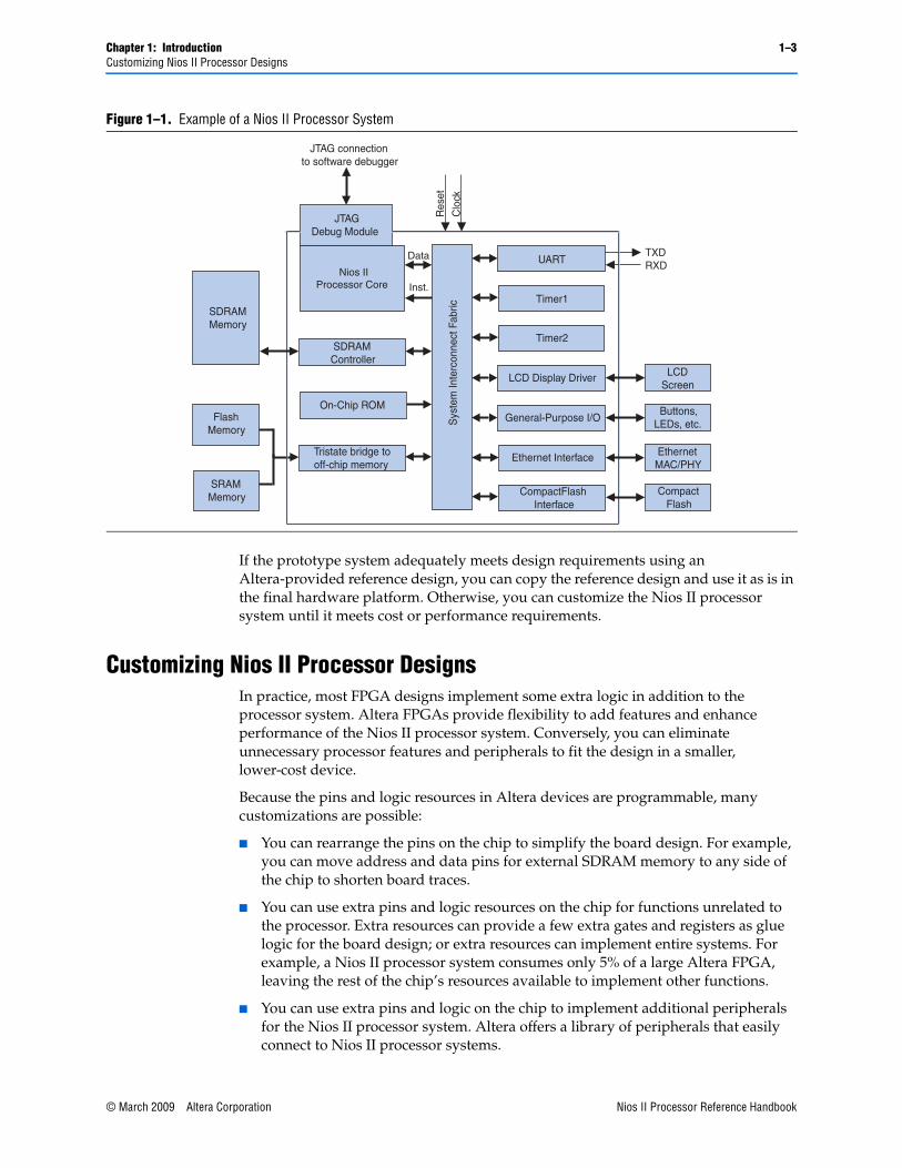
Using the Nios II hardware reference designs included in an Altera development kit, you can prototype an application running on a board before building a custom hardware platform. Figure 1–1 shows an example of a Nios II processor reference design available in an Altera Nios II development kit.
Nios II Processor Reference Handbook © March 2009 Altera CorporationPreliminary
Chapter 1: Introduction 1–3Customizing Nios II Processor Designs
If the prototype system adequately meets design requirements using an Altera-provided reference design, you can copy the reference design and use it as is in the final hardware platform. Otherwise, you can customize the Nios II processor system until it meets cost or performance requirements.
Customizing Nios II Processor DesignsIn practice, most FPGA designs implement some extra logic in addition to the processor system. Altera FPGAs provide flexibility to add features and enhance performance of the Nios II processor system. Conversely, you can eliminate unnecessary processor features and peripherals to fit the design in a smaller, lower-cost device.
Because the pins and logic resources in Altera devices are programmable, many customizations are possible:
■ You can rearrange the pins on the chip to simplify the board design. For example, you can move address and data pins for external SDRAM memory to any side of the chip to shorten board traces.
■ You can use extra pins and logic resources on the chip for functions unrelated to the processor. Extra resources can provide a few extra gates and registers as glue logic for the board design; or extra resources can implement entire systems. For example, a Nios II processor system consumes only 5% of a large Altera FPGA, leaving the rest of the chip’s resources available to implement other functions.
■ You can use extra pins and logic on the chip to implement additional peripherals for the Nios II processor system. Altera offers a library of peripherals that easily connect to Nios II processor systems.
Figure 1–1. Example of a Nios II Processor System
Nios IIProcessor Core
SDRAMController
On-Chip ROM
Tristate bridge tooff-chip memory
Sys
tem
Inte
rcon
nect
Fab
ric
JTAG Debug Module
SDRAMMemory
FlashMemory
SRAMMemory
UART
Timer1
Timer2
LCD Display Driver
General-Purpose I/O
Ethernet Interface
CompactFlash Interface
LCD Screen
EthernetMAC/PHY
Compact Flash
Buttons, LEDs, etc.
TXDRXD
JTAG connectionto software debugger
Clo
ck
Res
et
Data
Inst.
© March 2009 Altera Corporation Nios II Processor Reference HandbookPreliminary
1–4 Chapter 1: IntroductionConfigurable Soft-Core Processor Concepts
Configurable Soft-Core Processor ConceptsThis section introduces Nios II concepts that are unique or different from other discrete microcontrollers. The concepts described in this section provide a foundation for understanding the rest of the features discussed in this document.
For the most part, these concepts relate to the flexibility available to hardware designers to fine tune system implementation. Software programmers generally are not affected by the hardware implementation details, and can write programs without awareness of the configurable nature of the Nios II processor core.
Configurable Soft-Core ProcessorThe Nios II processor is a configurable soft-core processor, as opposed to a fixed, off-the-shelf microcontroller. In this context, configurable means that you can add or remove features on a system-by-system basis to meet performance or price goals. Soft-core means the processor core is not fixed in silicon and can be targeted to any Altera FPGA family.
Configurability does not require you to create a new Nios II processor configuration for every new design. Altera provides ready-made Nios II system designs that you can use as is. If these designs meet your system requirements, there is no need to configure the design further. In addition, software designers can use the Nios II instruction set simulator to begin writing and debugging Nios II applications before the final hardware configuration is determined.
Flexible Peripheral Set and Address MapA flexible peripheral set is one of the most notable differences between Nios II processor systems and fixed microcontrollers. Because of the soft-core nature of the Nios II processor, you can easily build made-to-order Nios II processor systems with the exact peripheral set required for the target applications.
A corollary of flexible peripherals is a flexible address map. Altera provides software constructs to access memory and peripherals generically, independently of address location. Therefore, the flexible peripheral set and address map does not affect application developers.
There are two broad classes of peripherals: standard peripherals and custom peripherals.
Standard PeripheralsAltera provides a set of peripherals commonly used in microcontrollers, such as timers, serial communication interfaces, general-purpose I/O, SDRAM controllers, and other memory interfaces. The list of available peripherals continues to grow as Altera and third-party vendors release new soft-peripheral cores.
f For details on the Altera-provided cores, refer to Volume 5: Embedded Peripherals of the Quartus II Handbook.
Nios II Processor Reference Handbook © March 2009 Altera CorporationPreliminary
Chapter 1: Introduction 1–5OpenCore Plus Evaluation
Custom PeripheralsYou can also create custom peripherals and integrate them in Nios II processor systems. For performance-critical systems that spend most CPU cycles executing a specific section of code, it is a common technique to create a custom peripheral that implements the same function in hardware. This approach offers a double performance benefit: the hardware implementation is faster than software; and the processor is free to perform other functions in parallel while the custom peripheral operates on data.
f For details on creating custom peripherals, refer to the SOPC Builder Components chapter in volume 4 of the Quartus II Handbook.
Custom InstructionsLike custom peripherals, custom instructions allow you to increase system performance by augmenting the processor with custom hardware. The soft-core nature of the Nios II processor enables you to integrate custom logic into the arithmetic logic unit (ALU). Similar to native Nios II instructions, custom instruction logic can take values from up to two source registers and optionally write back a result to a destination register.
Because the processor is implemented on reprogrammable Altera FPGAs, software and hardware engineers can work together to iteratively optimize the hardware and test the results of software running on hardware.
From the software perspective, custom instructions appear as machine-generated assembly macros or C functions, so programmers do not need to understand assembly language to use custom instructions.
Automated System GenerationAltera’s SOPC Builder design tool fully automates the process of configuring processor features and generating a hardware design that you program in an FPGA. The SOPC Builder graphical user interface (GUI) enables you to configure Nios II processor systems with any number of peripherals and memory interfaces. You can create entire processor systems without performing any schematic or hardware description-language (HDL) design entry. SOPC Builder can also import HDL design files, providing an easy mechanism to integrate custom logic in a Nios II processor system.
After system generation, you can download the design onto a board, and debug software executing on the board. To the software developer, the processor architecture of the design is set. Software development proceeds in the same manner as for traditional, non-configurable processors.
OpenCore Plus EvaluationYou can evaluate the Nios II processor without a license. With Altera's free OpenCore Plus evaluation feature, you can perform the following actions:
■ Simulate the behavior of a Nios II processor within your system
■ Verify the functionality of your design, as well as evaluate its size and speed quickly and easily
© March 2009 Altera Corporation Nios II Processor Reference HandbookPreliminary
1–6 Chapter 1: IntroductionReferenced Documents
■ Generate time-limited device programming files for designs that include Nios II processors
■ Program a device and verify your design in hardware
You only need to purchase a license for the Nios II processor when you are completely satisfied with its functionality and performance, and want to take your design to production.
f For more information about OpenCore Plus, refer to AN 320: OpenCore Plus Evaluation of Megafunctions.
Referenced DocumentsThis chapter references the following documents:
■ Volume 5: Embedded Peripherals of the Quartus II Handbook
■ SOPC Builder Components chapter in volume 4 of the Quartus II Handbook
■ AN 320: OpenCore Plus Evaluation of Megafunctions
■ Literature: Nios II Processor page on the Altera website
Document Revision HistoryTable 1–1 shows the revision history for this document.
Table 1–1. Document Revision History (Part 1 of 2)
Date & Document Version Changes Made Summary of Changes
March 2009
v9.0.0
Maintenance release. —
November 2008
v8.1.0
Maintenance release. —
May 2008
v8.0.0
Added MMU and MPU to bullet list of features. Added MMU and MPU.
October 2007
v7.2.0
Added OpenCore Plus section. —
May 2007
v7.1.0
■ Added table of contents to Introduction section.
■ Added Referenced Documents section.
—
March 2007
v7.0.0
Maintenance release. —
November 2006
v6.1.0
Maintenance release. —
May 2006
v6.0.0
■ Added single precision floating-point and integration with SignalTap® II logic analyzer to features list.
■ Updated performance to 250 DMIPS.
—
Nios II Processor Reference Handbook © March 2009 Altera CorporationPreliminary
Chapter 1: Introduction 1–7Document Revision History
October 2005
v5.1.0
Maintenance release. —
May 2005
v5.0.0
Maintenance release. —
September 2004
v1.1
Updates for Nios II 1.01 release. —
May 2004
v1.0
Initial release. —
Table 1–1. Document Revision History (Part 2 of 2)
Date & Document Version Changes Made Summary of Changes
© March 2009 Altera Corporation Nios II Processor Reference HandbookPreliminary

1–8 Chapter 1: IntroductionDocument Revision History
Nios II Processor Reference Handbook © March 2009 Altera CorporationPreliminary
© March 2009 Altera Corporation
NII51002-9.0.0
2. Processor Architecture
IntroductionThis chapter describes the hardware structure of the Nios® II processor, including a discussion of all the functional units of the Nios II architecture and the fundamentals of the Nios II processor hardware implementation. This chapter contains the following sections:
■ “Processor Implementation” on page 2–3
■ “Register File” on page 2–3
■ “Arithmetic Logic Unit” on page 2–3
■ “Reset and Debug Signals” on page 2–7
■ “Exception and Interrupt Controller” on page 2–7
■ “Memory and I/O Organization” on page 2–9
■ “JTAG Debug Module” on page 2–16
The Nios II architecture describes an instruction set architecture (ISA). The ISA in turn necessitates a set of functional units that implement the instructions. A Nios II processor core is a hardware design that implements the Nios II instruction set and supports the functional units described in this document. The processor core does not include peripherals or the connection logic to the outside world. It includes only the circuits required to implement the Nios II architecture.
Figure 2–1 shows a block diagram of the Nios II processor core.
Nios II Processor Reference HandbookPreliminary
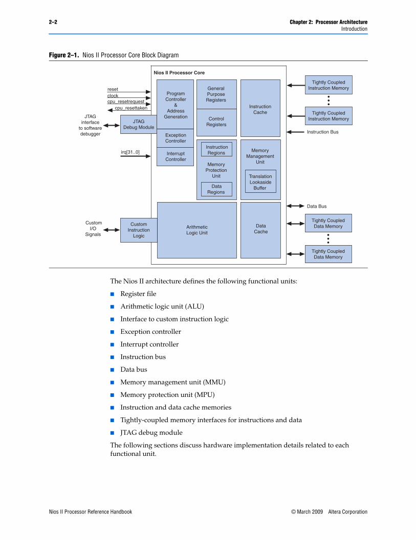
2–2 Chapter 2: Processor ArchitectureIntroduction
The Nios II architecture defines the following functional units:
■ Register file
■ Arithmetic logic unit (ALU)
■ Interface to custom instruction logic
■ Exception controller
■ Interrupt controller
■ Instruction bus
■ Data bus
■ Memory management unit (MMU)
■ Memory protection unit (MPU)
■ Instruction and data cache memories
■ Tightly-coupled memory interfaces for instructions and data
■ JTAG debug module
The following sections discuss hardware implementation details related to each functional unit.
Figure 2–1. Nios II Processor Core Block Diagram
ExceptionController
InterruptController
ArithmeticLogic Unit
GeneralPurposeRegisters
Control Registers
Nios II Processor Core
resetclock
JTAGinterface
to softwaredebugger
CustomI/O
Signals
irq[31..0]
JTAGDebug Module
ProgramController
&Address
Generation
CustomInstruction
Logic
Data Bus
Tightly CoupledData Memory
Tightly CoupledData Memory
DataCache
InstructionCache
Instruction Bus
Tightly CoupledInstruction Memory
Tightly CoupledInstruction Memory
cpu_resetrequestcpu_resettaken
MemoryManagement
Unit
Translation Lookaside
Buffer
InstructionRegions
MemoryProtection
Unit
DataRegions
Nios II Processor Reference Handbook © March 2009 Altera CorporationPreliminary
Chapter 2: Processor Architecture 2–3Processor Implementation
Processor ImplementationThe functional units of the Nios II architecture form the foundation for the Nios II instruction set. However, this does not indicate that any unit is implemented in hardware. The Nios II architecture describes an instruction set, not a particular hardware implementation. A functional unit can be implemented in hardware, emulated in software, or omitted entirely.
A Nios II implementation is a set of design choices embodied by a particular Nios II processor core. All implementations support the instruction set defined in the Instruction Set Reference chapter of the Nios II Processor Reference Handbook. Each implementation achieves specific objectives, such as smaller core size or higher performance. This allows the Nios II architecture to adapt to the needs of different target applications.
Implementation variables generally fit one of three trade-off patterns: more-or-less of a feature; inclusion-or-exclusion of a feature; hardware implementation or software emulation of a feature. An example of each trade-off follows:
■ More or less of a feature—For example, to fine-tune performance, you can increase or decrease the amount of instruction cache memory. A larger cache increases execution speed of large programs, while a smaller cache conserves on-chip memory resources.
■ Inclusion or exclusion of a feature—For example, to reduce cost, you can choose to omit the JTAG debug module. This decision conserves on-chip logic and memory resources, but it eliminates the ability to use a software debugger to debug applications.
■ Hardware implementation or software emulation—For example, in control applications that rarely perform complex arithmetic, you can choose for the division instruction to be emulated in software. Removing the divide hardware conserves on-chip resources but increases the execution time of division operations.
f For details of which Nios II cores supports what features, refer to the Nios II Core Implementation Details chapter of the Nios II Processor Reference Handbook. For complete details of user-selectable parameters for the Nios II processor, refer to the Instantiating the Nios II Processor in SOPC Builder chapter of the Nios II Processor Reference Handbook.
Register FileThe Nios II architecture supports a flat register file, consisting of thirty two 32-bit general-purpose integer registers, and up to thirty two 32-bit control registers. The architecture supports supervisor and user modes that allow system code to protect the control registers from errant applications.
The Nios II architecture allows for the future addition of floating-point registers.
Arithmetic Logic UnitThe Nios II ALU operates on data stored in general-purpose registers. ALU operations take one or two inputs from registers, and store a result back in a register. The ALU supports the data operations shown in Table 2–1.
© March 2009 Altera Corporation Nios II Processor Reference HandbookPreliminary
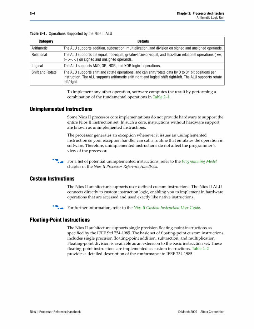
2–4 Chapter 2: Processor ArchitectureArithmetic Logic Unit
To implement any other operation, software computes the result by performing a combination of the fundamental operations in Table 2–1.
Unimplemented InstructionsSome Nios II processor core implementations do not provide hardware to support the entire Nios II instruction set. In such a core, instructions without hardware support are known as unimplemented instructions.
The processor generates an exception whenever it issues an unimplemented instruction so your exception handler can call a routine that emulates the operation in software. Therefore, unimplemented instructions do not affect the programmer’s view of the processor.
f For a list of potential unimplemented instructions, refer to the Programming Model chapter of the Nios II Processor Reference Handbook.
Custom InstructionsThe Nios II architecture supports user-defined custom instructions. The Nios II ALU connects directly to custom instruction logic, enabling you to implement in hardware operations that are accessed and used exactly like native instructions.
f For further information, refer to the Nios II Custom Instruction User Guide.
Floating-Point InstructionsThe Nios II architecture supports single precision floating-point instructions as specified by the IEEE Std 754-1985. The basic set of floating-point custom instructions includes single precision floating-point addition, subtraction, and multiplication. Floating-point division is available as an extension to the basic instruction set. These floating-point instructions are implemented as custom instructions. Table 2–2 provides a detailed description of the conformance to IEEE 754-1985.
Table 2–1. Operations Supported by the Nios II ALU
Category Details
Arithmetic The ALU supports addition, subtraction, multiplication, and division on signed and unsigned operands.
Relational The ALU supports the equal, not-equal, greater-than-or-equal, and less-than relational operations ( ==, != >=, < ) on signed and unsigned operands.
Logical The ALU supports AND, OR, NOR, and XOR logical operations.
Shift and Rotate The ALU supports shift and rotate operations, and can shift/rotate data by 0 to 31 bit positions per instruction. The ALU supports arithmetic shift right and logical shift right/left. The ALU supports rotate left/right.
Nios II Processor Reference Handbook © March 2009 Altera CorporationPreliminary
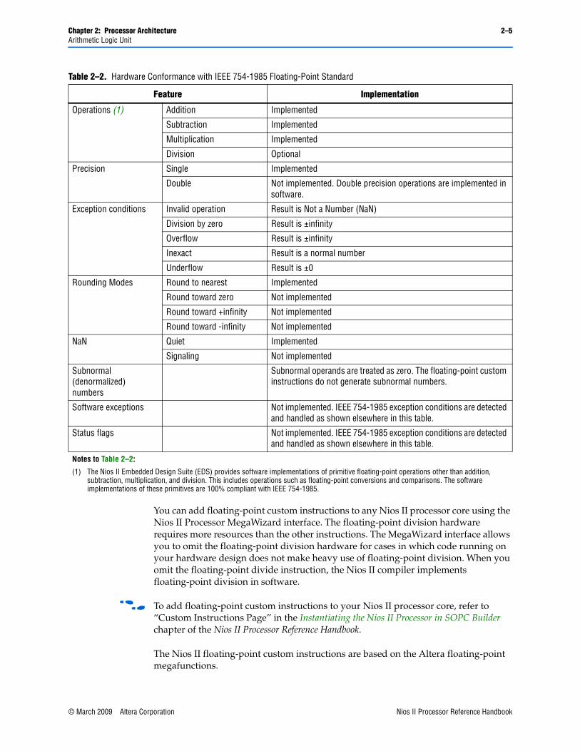
Chapter 2: Processor Architecture 2–5Arithmetic Logic Unit
You can add floating-point custom instructions to any Nios II processor core using the Nios II Processor MegaWizard interface. The floating-point division hardware requires more resources than the other instructions. The MegaWizard interface allows you to omit the floating-point division hardware for cases in which code running on your hardware design does not make heavy use of floating-point division. When you omit the floating-point divide instruction, the Nios II compiler implements floating-point division in software.
f To add floating-point custom instructions to your Nios II processor core, refer to “Custom Instructions Page” in the Instantiating the Nios II Processor in SOPC Builder chapter of the Nios II Processor Reference Handbook.
The Nios II floating-point custom instructions are based on the Altera floating-point megafunctions.
Table 2–2. Hardware Conformance with IEEE 754-1985 Floating-Point Standard
Feature Implementation
Operations (1) Addition Implemented
Subtraction Implemented
Multiplication Implemented
Division Optional
Precision Single Implemented
Double Not implemented. Double precision operations are implemented in software.
Exception conditions Invalid operation Result is Not a Number (NaN)
Division by zero Result is ±infinity
Overflow Result is ±infinity
Inexact Result is a normal number
Underflow Result is ±0
Rounding Modes Round to nearest Implemented
Round toward zero Not implemented
Round toward +infinity Not implemented
Round toward -infinity Not implemented
NaN Quiet Implemented
Signaling Not implemented
Subnormal (denormalized) numbers
Subnormal operands are treated as zero. The floating-point custom instructions do not generate subnormal numbers.
Software exceptions Not implemented. IEEE 754-1985 exception conditions are detected and handled as shown elsewhere in this table.
Status flags Not implemented. IEEE 754-1985 exception conditions are detected and handled as shown elsewhere in this table.
Notes to Table 2–2:
(1) The Nios II Embedded Design Suite (EDS) provides software implementations of primitive floating-point operations other than addition, subtraction, multiplication, and division. This includes operations such as floating-point conversions and comparisons. The software implementations of these primitives are 100% compliant with IEEE 754-1985.
© March 2009 Altera Corporation Nios II Processor Reference HandbookPreliminary
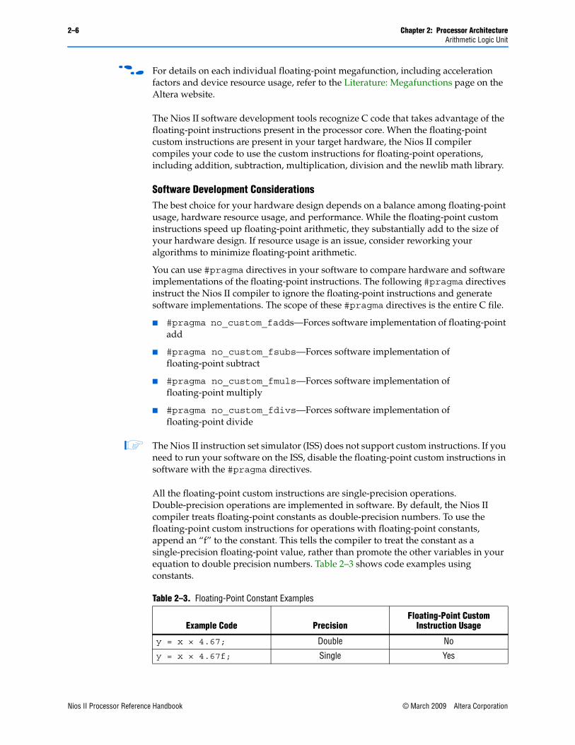
2–6 Chapter 2: Processor ArchitectureArithmetic Logic Unit
f For details on each individual floating-point megafunction, including acceleration factors and device resource usage, refer to the Literature: Megafunctions page on the Altera website.
The Nios II software development tools recognize C code that takes advantage of the floating-point instructions present in the processor core. When the floating-point custom instructions are present in your target hardware, the Nios II compiler compiles your code to use the custom instructions for floating-point operations, including addition, subtraction, multiplication, division and the newlib math library.
Software Development ConsiderationsThe best choice for your hardware design depends on a balance among floating-point usage, hardware resource usage, and performance. While the floating-point custom instructions speed up floating-point arithmetic, they substantially add to the size of your hardware design. If resource usage is an issue, consider reworking your algorithms to minimize floating-point arithmetic.
You can use #pragma directives in your software to compare hardware and software implementations of the floating-point instructions. The following #pragma directives instruct the Nios II compiler to ignore the floating-point instructions and generate software implementations. The scope of these #pragma directives is the entire C file.
■ #pragma no_custom_fadds—Forces software implementation of floating-point add
■ #pragma no_custom_fsubs—Forces software implementation of floating-point subtract
■ #pragma no_custom_fmuls—Forces software implementation of floating-point multiply
■ #pragma no_custom_fdivs—Forces software implementation of floating-point divide
1 The Nios II instruction set simulator (ISS) does not support custom instructions. If you need to run your software on the ISS, disable the floating-point custom instructions in software with the #pragma directives.
All the floating-point custom instructions are single-precision operations. Double-precision operations are implemented in software. By default, the Nios II compiler treats floating-point constants as double-precision numbers. To use the floating-point custom instructions for operations with floating-point constants, append an “f” to the constant. This tells the compiler to treat the constant as a single-precision floating-point value, rather than promote the other variables in your equation to double precision numbers. Table 2–3 shows code examples using constants.
Table 2–3. Floating-Point Constant Examples
Example Code PrecisionFloating-Point Custom
Instruction Usage
y = x × 4.67; Double No
y = x × 4.67f; Single Yes
Nios II Processor Reference Handbook © March 2009 Altera CorporationPreliminary
Chapter 2: Processor Architecture 2–7Reset and Debug Signals
Reset and Debug SignalsThe Nios II processor core supports the following two kinds of reset signals:
■ reset—This is a global hardware reset signal that forces the processor core to reset immediately.
■ cpu_resetrequest—This is an optional, local reset signal that causes the processor to reset without affecting other components in the Nios II system. The processor finishes executing any instructions in the pipeline, and then enters the reset state. This process can take several clock cycles, so be sure to continue asserting the cpu_resetrequest signal until the processor core asserts a cpu_resettaken signal.
The processor core asserts a cpu_resettaken signal for 1 cycle when the reset is complete and then periodically if cpu_resetrequest remains asserted. The processor remains in the reset state for as long as cpu_resetrequest is asserted. While the processor is in the reset state, it periodically reads from the reset address. It discards the result of the read, and remains in the reset state.
The processor does not respond to cpu_resetrequest when the processor is under the control of the JTAG debug module, that is, when the processor is paused. The processor responds to the cpu_resetrequest signal if the signal is asserted when the JTAG debug module relinquishes control, both momentarily during each single step as well as when you resume execution.
f For more information on adding reset signals to the Nios II processor, refer to “Advanced Features Page” in the Instantiating the Nios II Processor in SOPC Builder chapter of the Nios II Processor Reference Handbook.
The Nios II processor core also supports debug signals.
■ debugreq—This is an optional signal that temporarily suspends the processor for debugging purposes. When you assert the signal, the processor pauses in the same manner as when a breakpoint is encountered, transfers execution to the routine located at the break address, and asserts a debugack signal. Asserting the debugreq signal when the processor is already paused has no effect.
f For more information on the break vector and adding debug signals to the Nios II processor, refer to “JTAG Debug Module Page” in the Instantiating the Nios II Processor in SOPC Builder chapter of the Nios II Processor Reference Handbook.
Exception and Interrupt Controller
Exception ControllerThe Nios II architecture provides a simple, non-vectored exception controller to handle all exception types. Each exception, including hardware interrupts, causes the processor to transfer execution to an exception address. An exception handler at this address determines the cause of the exception and dispatches an appropriate exception routine.
Exception addresses are specified in SOPC Builder at system generation time.
© March 2009 Altera Corporation Nios II Processor Reference HandbookPreliminary
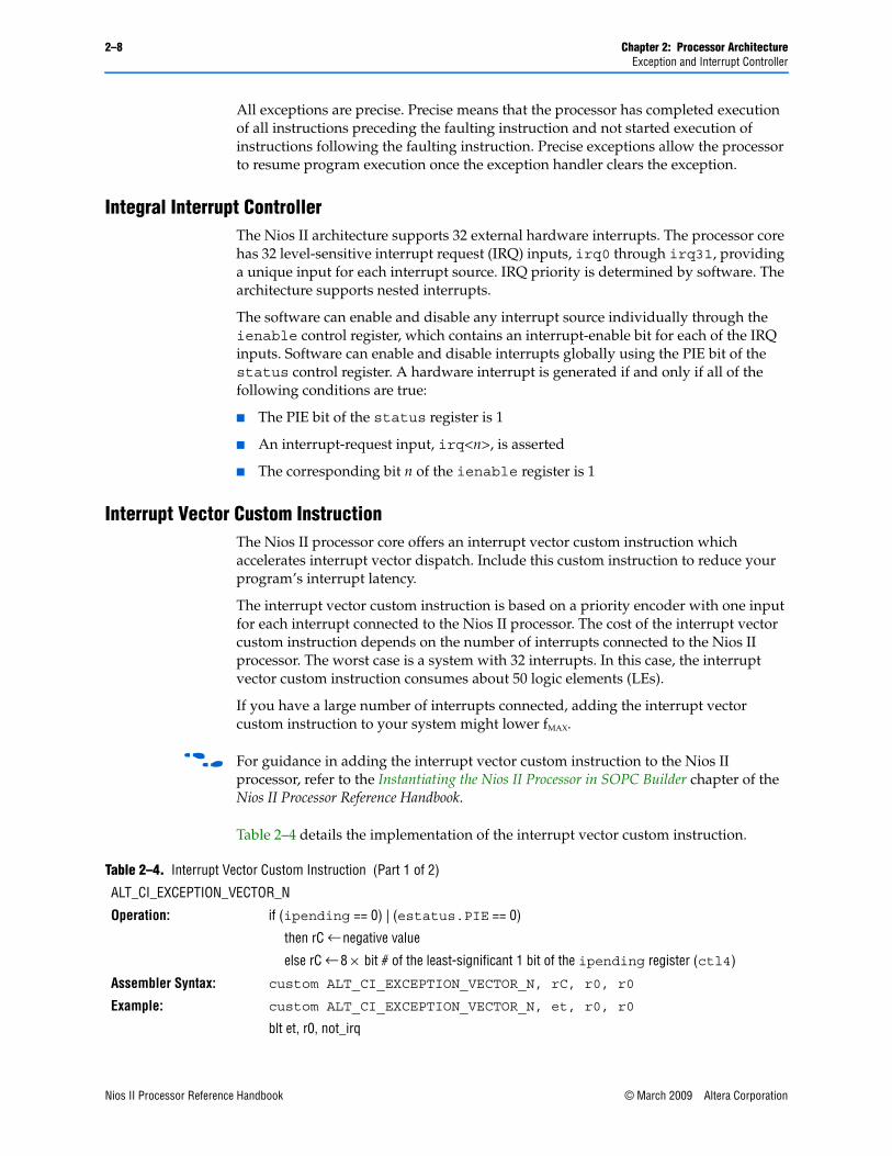
2–8 Chapter 2: Processor ArchitectureException and Interrupt Controller
All exceptions are precise. Precise means that the processor has completed execution of all instructions preceding the faulting instruction and not started execution of instructions following the faulting instruction. Precise exceptions allow the processor to resume program execution once the exception handler clears the exception.
Integral Interrupt ControllerThe Nios II architecture supports 32 external hardware interrupts. The processor core has 32 level-sensitive interrupt request (IRQ) inputs, irq0 through irq31, providing a unique input for each interrupt source. IRQ priority is determined by software. The architecture supports nested interrupts.
The software can enable and disable any interrupt source individually through the ienable control register, which contains an interrupt-enable bit for each of the IRQ inputs. Software can enable and disable interrupts globally using the PIE bit of the status control register. A hardware interrupt is generated if and only if all of the following conditions are true:
■ The PIE bit of the status register is 1
■ An interrupt-request input, irq<n>, is asserted
■ The corresponding bit n of the ienable register is 1
Interrupt Vector Custom InstructionThe Nios II processor core offers an interrupt vector custom instruction which accelerates interrupt vector dispatch. Include this custom instruction to reduce your program’s interrupt latency.
The interrupt vector custom instruction is based on a priority encoder with one input for each interrupt connected to the Nios II processor. The cost of the interrupt vector custom instruction depends on the number of interrupts connected to the Nios II processor. The worst case is a system with 32 interrupts. In this case, the interrupt vector custom instruction consumes about 50 logic elements (LEs).
If you have a large number of interrupts connected, adding the interrupt vector custom instruction to your system might lower fMAX.
f For guidance in adding the interrupt vector custom instruction to the Nios II processor, refer to the Instantiating the Nios II Processor in SOPC Builder chapter of the Nios II Processor Reference Handbook.
Table 2–4 details the implementation of the interrupt vector custom instruction.
Table 2–4. Interrupt Vector Custom Instruction (Part 1 of 2)
ALT_CI_EXCEPTION_VECTOR_N
Operation: if (ipending == 0) | (estatus.PIE == 0)
then rC ← negative value
else rC ← 8 × bit # of the least-significant 1 bit of the ipending register (ctl4)
Assembler Syntax: custom ALT_CI_EXCEPTION_VECTOR_N, rC, r0, r0
Example: custom ALT_CI_EXCEPTION_VECTOR_N, et, r0, r0
blt et, r0, not_irq
Nios II Processor Reference Handbook © March 2009 Altera CorporationPreliminary
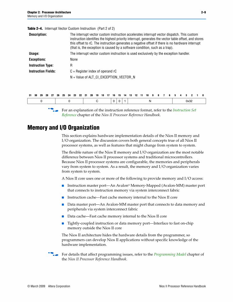
Chapter 2: Processor Architecture 2–9Memory and I/O Organization
f For an explanation of the instruction reference format, refer to the Instruction Set Reference chapter of the Nios II Processor Reference Handbook.
Memory and I/O OrganizationThis section explains hardware implementation details of the Nios II memory and I/O organization. The discussion covers both general concepts true of all Nios II processor systems, as well as features that might change from system to system.
The flexible nature of the Nios II memory and I/O organization are the most notable difference between Nios II processor systems and traditional microcontrollers. Because Nios II processor systems are configurable, the memories and peripherals vary from system to system. As a result, the memory and I/O organization varies from system to system.
A Nios II core uses one or more of the following to provide memory and I/O access:
■ Instruction master port—An Avalon® Memory-Mapped (Avalon-MM) master port that connects to instruction memory via system interconnect fabric
■ Instruction cache—Fast cache memory internal to the Nios II core
■ Data master port—An Avalon-MM master port that connects to data memory and peripherals via system interconnect fabric
■ Data cache—Fast cache memory internal to the Nios II core
■ Tightly-coupled instruction or data memory port—Interface to fast on-chip memory outside the Nios II core
The Nios II architecture hides the hardware details from the programmer, so programmers can develop Nios II applications without specific knowledge of the hardware implementation.
f For details that affect programming issues, refer to the Programming Model chapter of the Nios II Processor Reference Handbook.
Description: The interrupt vector custom instruction accelerates interrupt vector dispatch. This custom instruction identifies the highest priority interrupt, generates the vector table offset, and stores this offset to rC. The instruction generates a negative offset if there is no hardware interrupt (that is, the exception is caused by a software condition, such as a trap).
Usage: The interrupt vector custom instruction is used exclusively by the exception handler.
Exceptions: None
Instruction Type: R
Instruction Fields: C = Register index of operand rC
N = Value of ALT_CI_EXCEPTION_VECTOR_N
31 30 29 28 27 26 25 24 23 22 21 20 19 18 17 16 15 14 13 12 11 10 9 8 7 6 5 4 3 2 1 0
0 0 C 0 0 1 N 0x32
Table 2–4. Interrupt Vector Custom Instruction (Part 2 of 2)
© March 2009 Altera Corporation Nios II Processor Reference HandbookPreliminary
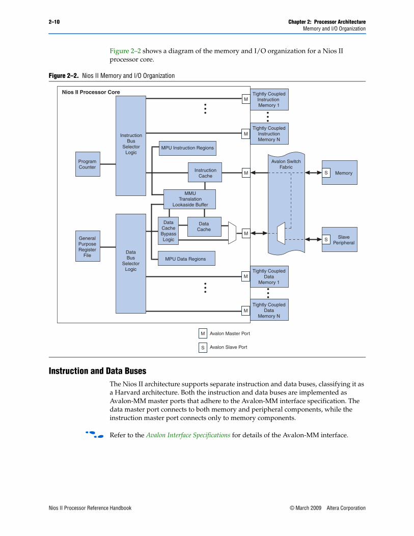
2–10 Chapter 2: Processor ArchitectureMemory and I/O Organization
Figure 2–2 shows a diagram of the memory and I/O organization for a Nios II processor core.
Instruction and Data BusesThe Nios II architecture supports separate instruction and data buses, classifying it as a Harvard architecture. Both the instruction and data buses are implemented as Avalon-MM master ports that adhere to the Avalon-MM interface specification. The data master port connects to both memory and peripheral components, while the instruction master port connects only to memory components.
f Refer to the Avalon Interface Specifications for details of the Avalon-MM interface.
Figure 2–2. Nios II Memory and I/O Organization
S
MemoryS
SlavePeripheral
Avalon Master Port
Avalon Slave Port
M
S
M
M
Tightly CoupledInstructionMemory N
Tightly CoupledData
Memory 1
InstructionCache
DataCache
Nios II Processor Core
Avalon SwitchFabric
ProgramCounter
GeneralPurposeRegister
File
InstructionBus
SelectorLogic
Tightly CoupledData
Memory N
Tightly CoupledInstruction Memory 1
DataBus
SelectorLogic
MMUTranslation
Lookaside Buffer
M
M
M
M
DataCacheBypassLogic
MPU Instruction Regions
MPU Data Regions
Nios II Processor Reference Handbook © March 2009 Altera CorporationPreliminary
Chapter 2: Processor Architecture 2–11Memory and I/O Organization
Memory and Peripheral AccessThe Nios II architecture provides memory-mapped I/O access. Both data memory and peripherals are mapped into the address space of the data master port. The Nios II architecture is little endian. Words and halfwords are stored in memory with the more-significant bytes at higher addresses.
The Nios II architecture does not specify anything about the existence of memory and peripherals; the quantity, type, and connection of memory and peripherals are system-dependent. Typically, Nios II processor systems contain a mix of fast on-chip memory and slower off-chip memory. Peripherals typically reside on-chip, although interfaces to off-chip peripherals also exist.
Instruction Master PortThe Nios II instruction bus is implemented as a 32-bit Avalon-MM master port. The instruction master port performs a single function: it fetches instructions to be executed by the processor. The instruction master port does not perform any write operations.
The instruction master port is a pipelined Avalon-MM master port. Support for pipelined Avalon-MM transfers minimizes the impact of synchronous memory with pipeline latency and increases the overall fMAX of the system. The instruction master port can issue successive read requests before data has returned from prior requests. The Nios II processor can prefetch sequential instructions and perform branch prediction to keep the instruction pipe as active as possible.
The instruction master port always retrieves 32 bits of data. The instruction master port relies on dynamic bus-sizing logic contained in the system interconnect fabric. By virtue of dynamic bus sizing, every instruction fetch returns a full instruction word, regardless of the width of the target memory. Consequently, programs do not need to be aware of the widths of memory in the Nios II processor system.
The Nios II architecture supports on-chip cache memory for improving average instruction fetch performance when accessing slower memory. Refer to “Cache Memory” on page 2–12 for details. The Nios II architecture supports tightly-coupled memory, which provides guaranteed low-latency access to on-chip memory. Refer to “Tightly-Coupled Memory” on page 2–13 for details.
Data Master PortThe Nios II data bus is implemented as a 32-bit Avalon-MM master port. The data master port performs two functions:
■ Read data from memory or a peripheral when the processor executes a load instruction
■ Write data to memory or a peripheral when the processor executes a store instruction
Byte-enable signals on the master port specify which of the four byte-lane(s) to write during store operations. When the Nios II core is configured with a data cache line size greater than four bytes, the data master port supports pipelined Avalon-MM transfers. When the data cache line size is only four bytes, any memory pipeline latency is perceived by the data master port as wait states. Load and store operations can complete in a single clock-cycle when the data master port is connected to zero-wait-state memory.
© March 2009 Altera Corporation Nios II Processor Reference HandbookPreliminary
2–12 Chapter 2: Processor ArchitectureMemory and I/O Organization
The Nios II architecture supports on-chip cache memory for improving average data transfer performance when accessing slower memory. Refer to “Cache Memory” on page 2–12 for details. The Nios II architecture supports tightly-coupled memory, which provides guaranteed low-latency access to on-chip memory. Refer to “Tightly-Coupled Memory” on page 2–13 for details.
Shared Memory for Instructions and Data Usually the instruction and data master ports share a single memory that contains both instructions and data. While the processor core has separate instruction and data buses, the overall Nios II processor system might present a single, shared instruction/data bus to the outside world. The outside view of the Nios II processor system depends on the memory and peripherals in the system and the structure of the system interconnect fabric.
The data and instruction master ports never cause a gridlock condition in which one port starves the other. For highest performance, assign the data master port higher arbitration priority on any memory that is shared by both instruction and data master ports.
Cache MemoryThe Nios II architecture supports cache memories on both the instruction master port (instruction cache) and the data master port (data cache). Cache memory resides on-chip as an integral part of the Nios II processor core. The cache memories can improve the average memory access time for Nios II processor systems that use slow off-chip memory such as SDRAM for program and data storage.
The instruction and data caches are enabled perpetually at run-time, but methods are provided for software to bypass the data cache so that peripheral accesses do not return cached data. Cache management and cache coherency are handled by software. The Nios II instruction set provides instructions for cache management.
Configurable Cache Memory OptionsThe cache memories are optional. The need for higher memory performance (and by association, the need for cache memory) is application dependent. Many applications require the smallest possible processor core, and can trade-off performance for size.
A Nios II processor core might include one, both, or neither of the cache memories. Furthermore, for cores that provide data and/or instruction cache, the sizes of the cache memories are user-configurable. The inclusion of cache memory does not affect the functionality of programs, but it does affect the speed at which the processor fetches instructions and reads/writes data.
Effective Use of Cache MemoryThe effectiveness of cache memory to improve performance is based on the following premises:
■ Regular memory is located off-chip, and access time is long compared to on-chip memory
■ The largest, performance-critical instruction loop is smaller than the instruction cache
■ The largest block of performance-critical data is smaller than the data cache
Nios II Processor Reference Handbook © March 2009 Altera CorporationPreliminary
Chapter 2: Processor Architecture 2–13Memory and I/O Organization
Optimal cache configuration is application specific, although you can make decisions that are effective across a range of applications. For example, if a Nios II processor system includes only fast, on-chip memory (i.e., it never accesses slow, off-chip memory), an instruction or data cache is unlikely to offer any performance gain. As another example, if the critical loop of a program is 2 KBytes, but the size of the instruction cache is 1 KByte, an instruction cache does not improve execution speed. In fact, an instruction cache may degrade performance in this situation.
If an application always requires certain data or sections of code to be located in cache memory for performance reasons, the tightly-coupled memory feature might provide a more appropriate solution. Refer to “Tightly-Coupled Memory” on page 2–13 for details.
Cache Bypass MethodsThe Nios II architecture provides the following methods for bypassing the data cache:
■ I/O load and store instructions
■ Bit-31 cache bypass
I/O Load and Store Instructions Method
The load and store I/O instructions such as ldio and stio bypass the data cache and force an Avalon-MM data transfer to a specified address.
The Bit-31 Cache Bypass Method
The bit-31 cache bypass method on the data master port uses bit 31 of the address as a tag that indicates whether the processor should transfer data to/from cache, or bypass it. This is a convenience for software, which might need to cache certain addresses and bypass others. Software can pass addresses as parameters between functions, without having to specify any further information about whether the addressed data is cached or not.
f To determine which cores implement which cache bypass methods, refer to the Nios II Core Implementation Details chapter of the Nios II Processor Reference Handbook.
Tightly-Coupled MemoryTightly-coupled memory provides guaranteed low-latency memory access for performance-critical applications. Compared to cache memory, tightly-coupled memory provides the following benefits:
■ Performance similar to cache memory
■ Software can guarantee that performance-critical code or data is located in tightly-coupled memory
■ No real-time caching overhead, such as loading, invalidating, or flushing memory
Physically, a tightly-coupled memory port is a separate master port on the Nios II processor core, similar to the instruction or data master port. A Nios II core can have zero, one, or multiple tightly-coupled memories. The Nios II architecture supports tightly-coupled memories for both instruction and data access. Each tightly-coupled memory port connects directly to exactly one memory with guaranteed low, fixed latency. The memory is external to the Nios II core and is usually located on chip.
© March 2009 Altera Corporation Nios II Processor Reference HandbookPreliminary
2–14 Chapter 2: Processor ArchitectureMemory and I/O Organization
Accessing Tightly-Coupled MemoryTightly-coupled memories occupy normal address space, the same as other memory devices connected via system interconnect fabric. The address ranges for tightly-coupled memories (if any) are determined at system generation time.
Software accesses tightly-coupled memory using regular load and store instructions. From the software’s perspective, there is no difference accessing tightly-coupled memory compared to other memory.
Effective Use of Tightly-Coupled MemoryA system can use tightly-coupled memory to achieve maximum performance for accessing a specific section of code or data. For example, interrupt-intensive applications can place exception handler code into a tightly-coupled memory to minimize interrupt latency. Similarly, compute-intensive digital signal processing (DSP) applications can place data buffers into tightly-coupled memory for the fastest possible data access.
If the application’s memory requirements are small enough to fit entirely on chip, it is possible to use tightly-coupled memory exclusively for code and data. Larger applications must selectively choose what to include in tightly-coupled memory to maximize the cost-performance trade-off.
Address MapThe address map for memories and peripherals in a Nios II processor system is design dependent. You specify the address map at system generation time.
There are three addresses that are part of the processor and deserve special mention:
■ Reset address
■ Exception address
■ Break handler address
Programmers access memories and peripherals by using macros and drivers. Therefore, the flexible address map does not affect application developers.
Memory Management UnitThe optional Nios II MMU provides the following features and functionality:
■ Virtual to physical address mapping
■ Memory protection
■ 32-bit virtual and physical addresses, mapping a 4 GByte virtual address space into as much as 4 GBytes of physical memory
■ 4 KByte page and frame size
■ Low 512 MBytes of physical address space available for direct access
Nios II Processor Reference Handbook © March 2009 Altera CorporationPreliminary
Chapter 2: Processor Architecture 2–15Memory and I/O Organization
■ Hardware translation lookaside buffers (TLBs), accelerating address translation
■ Separate TLBs for instruction and data accesses
■ Read, write, and execute permissions controlled per page
■ Default caching behavior controlled per page
■ TLBs acting as n-way set-associative caches for software page tables
■ TLB sizes and associativities configurable at system generation
■ Format of page tables (or equivalent data structures) determined by system software
■ Replacement policy for TLB entries determined by system software
■ Write policy for TLB entries determined by system software
■ All exceptions precise
f For further details on the MMU implementation, refer to the Programming Model chapter of the Nios II Processor Reference Handbook.
You can optionally include the MMU when you instantiate the Nios II processor in your Nios II hardware system. When present, the MMU is always enabled, and the data and instruction caches are virtually-indexed, physically-tagged caches. Several parameters are available, allowing you to optimize the MMU for your system needs.
For complete details of user-selectable parameters for the Nios II MMU, refer to the Instantiating the Nios II Processor in SOPC Builder chapter of the Nios II Processor Reference Handbook.
1 The Nios II MMU is optional and mutually exclusive from the Nios II MPU. Nios II systems can include either an MMU or MPU, but cannot include both an MMU and MPU in the same design.
Memory Protection UnitThe optional Nios II MPU provides the following features and functionality:
■ Memory protection
■ Up to 32 instruction regions and 32 data regions
■ Variable instruction and data region sizes
■ Amount of region memory defined by size or upper address limit
■ Read and write access permissions for data regions
■ Execute access permissions for instruction regions
■ Overlapping regions
■ All exceptions precise
f For further details on the MPU implementation, refer to the Programming Model chapter of the Nios II Processor Reference Handbook.
© March 2009 Altera Corporation Nios II Processor Reference HandbookPreliminary
2–16 Chapter 2: Processor ArchitectureJTAG Debug Module
You can optionally include the MPU when you instantiate the Nios II processor in your Nios II hardware system. When present, the MPU is always enabled. Several parameters are available, allowing you to optimize the MPU for your system needs.
f For complete details of user-selectable parameters for the Nios II MPU, refer to the Instantiating the Nios II Processor in SOPC Builder chapter of the Nios II Processor Reference Handbook.
1 The Nios II MPU is optional and mutually exclusive from the Nios II MMU. Nios II systems can include either an MPU or MMU, but cannot include both an MPU and MMU in the same design.
JTAG Debug ModuleThe Nios II architecture supports a JTAG debug module that provides on-chip emulation features to control the processor remotely from a host PC. PC-based software debugging tools communicate with the JTAG debug module and provide facilities, such as the following features:
■ Downloading programs to memory
■ Starting and stopping execution
■ Setting breakpoints and watchpoints
■ Analyzing registers and memory
■ Collecting real-time execution trace data
1 The Nios II MMU does not support the JTAG debug module trace.
The debug module connects to the JTAG circuitry in an Altera® FPGA. External debugging probes can then access the processor via the standard JTAG interface on the FPGA. On the processor side, the debug module connects to signals inside the processor core. The debug module has non-maskable control over the processor, and does not require a software stub linked into the application under test. All system resources visible to the processor in supervisor mode are available to the debug module. For trace data collection, the debug module stores trace data in memory either on-chip or in the debug probe.
The debug module gains control of the processor either by asserting a hardware break signal, or by writing a break instruction into program memory to be executed. In both cases, the processor transfers execution to the routine located at the break address. The break address is specified in SOPC Builder at system generation time.
Soft-core processors such as the Nios II processor offer unique debug capabilities beyond the features of traditional, fixed processors. The soft-core nature of the Nios II processor allows you to debug a system in development using a full-featured debug core, and later remove the debug features to conserve logic resources. For the release version of a product, the JTAG debug module functionality can be reduced, or removed altogether.
Nios II Processor Reference Handbook © March 2009 Altera CorporationPreliminary
Chapter 2: Processor Architecture 2–17JTAG Debug Module
The following sections describe the capabilities of the Nios II JTAG debug module hardware. The usage of all hardware features is dependent on host software, such as the Nios II IDE, which manages the connection to the target processor and controls the debug process.
JTAG Target ConnectionThe JTAG target connection provides the ability to connect to the processor through the standard JTAG pins on the Altera FPGA. This provides basic capabilities to start and stop the processor, and examine and edit registers and memory. The JTAG target connection is the minimum requirement for the Nios II IDE flash programmer.
1 While the processor has no minimum clock frequency requirements, Altera recommends that your design’s system clock frequency be at least four times the JTAG clock frequency to ensure that the on-chip instrumentation (OCI) core functions properly.
Download and Execute SoftwareDownloading software refers to the ability to download executable code and data to the processor’s memory via the JTAG connection. After downloading software to memory, the JTAG debug module can then exit debug mode and transfer execution to the start of executable code.
Software BreakpointsSoftware breakpoints allow you to set a breakpoint on instructions residing in RAM. The software breakpoint mechanism writes a break instruction into executable code stored in RAM. When the processor executes the break instruction, control is transferred to the JTAG debug module.
Hardware BreakpointsHardware breakpoints allow you to set a breakpoint on instructions residing in nonvolatile memory, such as flash memory. The hardware breakpoint mechanism continuously monitors the processor’s current instruction address. If the instruction address matches the hardware breakpoint address, the JTAG debug module takes control of the processor.
Hardware breakpoints are implemented using the JTAG debug module’s hardware trigger feature.
Hardware TriggersHardware triggers activate a debug action based on conditions on the instruction or data bus during real-time program execution. Triggers can do more than halt processor execution. For example, a trigger can be used to enable trace data collection during real-time processor execution.
Table 2–5 lists all the conditions that can cause a trigger. Hardware trigger conditions are based on either the instruction or data bus. Trigger conditions on the same bus can be logically ANDed, enabling the JTAG debug module to trigger, for example, only on write cycles to a specific address.
© March 2009 Altera Corporation Nios II Processor Reference HandbookPreliminary
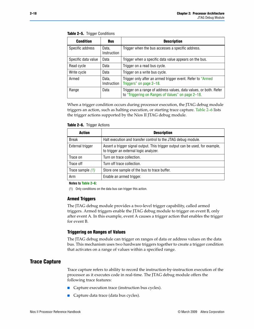
2–18 Chapter 2: Processor ArchitectureJTAG Debug Module
When a trigger condition occurs during processor execution, the JTAG debug module triggers an action, such as halting execution, or starting trace capture. Table 2–6 lists the trigger actions supported by the Nios II JTAG debug module.
Armed Triggers The JTAG debug module provides a two-level trigger capability, called armed triggers. Armed triggers enable the JTAG debug module to trigger on event B, only after event A. In this example, event A causes a trigger action that enables the trigger for event B.
Triggering on Ranges of Values The JTAG debug module can trigger on ranges of data or address values on the data bus. This mechanism uses two hardware triggers together to create a trigger condition that activates on a range of values within a specified range.
Trace CaptureTrace capture refers to ability to record the instruction-by-instruction execution of the processor as it executes code in real-time. The JTAG debug module offers the following trace features:
■ Capture execution trace (instruction bus cycles).
■ Capture data trace (data bus cycles).
Table 2–5. Trigger Conditions
Condition Bus Description
Specific address Data, Instruction
Trigger when the bus accesses a specific address.
Specific data value Data Trigger when a specific data value appears on the bus.
Read cycle Data Trigger on a read bus cycle.
Write cycle Data Trigger on a write bus cycle.
Armed Data, Instruction
Trigger only after an armed trigger event. Refer to “Armed Triggers” on page 2–18.
Range Data Trigger on a range of address values, data values, or both. Refer to “Triggering on Ranges of Values” on page 2–18.
Table 2–6. Trigger Actions
Action Description
Break Halt execution and transfer control to the JTAG debug module.
External trigger Assert a trigger signal output. This trigger output can be used, for example, to trigger an external logic analyzer.
Trace on Turn on trace collection.
Trace off Turn off trace collection.
Trace sample (1) Store one sample of the bus to trace buffer.
Arm Enable an armed trigger.
Notes to Table 2–6:
(1) Only conditions on the data bus can trigger this action.
Nios II Processor Reference Handbook © March 2009 Altera CorporationPreliminary
Chapter 2: Processor Architecture 2–19JTAG Debug Module
■ For each data bus cycle, capture address, data, or both.
■ Start and stop capturing trace in real time, based on triggers.
■ Manually start and stop trace under host control.
■ Optionally stop capturing trace when trace buffer is full, leaving the processor executing.
■ Store trace data in on-chip memory buffer in the JTAG debug module. (This memory is accessible only through the JTAG connection.)
■ Store trace data to larger buffers in an off-chip debug probe.
Certain trace features require additional licensing or debug tools from third-party debug providers. For example, an on-chip trace buffer is a standard feature of the Nios II processor, but using an off-chip trace buffer requires additional debug software and hardware provided by First Silicon Solutions (FS2) or Lauterbach GmbH.
f For details, refer to the FS2 website ( www.fs2.com) and the Lauterbach GmbH website (www.lauterbach.com).
Execution vs. Data Trace The JTAG debug module supports tracing the instruction bus (execution trace), the data bus (data trace), or both simultaneously. Execution trace records only the addresses of the instructions executed, enabling you to analyze where in memory (i.e., in which functions) code executed. Data trace records the data associated with each load and store operation on the data bus.
The JTAG debug module can filter the data bus trace in real time to capture the following:
■ Load addresses only
■ Store addresses only
■ Both load and store addresses
■ Load data only
■ Load address and data
■ Store address and data
■ Address and data for both loads and stores
■ Single sample of the data bus upon trigger event
Trace FramesA frame is a unit of memory allocated for collecting trace data. However, a frame is not an absolute measure of the trace depth.
© March 2009 Altera Corporation Nios II Processor Reference HandbookPreliminary
2–20 Chapter 2: Processor ArchitectureReferenced Documents
To keep pace with the processor executing in real time, execution trace is optimized to store only selected addresses, such as branches, calls, traps, and interrupts. From these addresses, host-side debug software can later reconstruct an exact instruction-by-instruction execution trace. Furthermore, execution trace data is stored in a compressed format, such that one frame represents more than one instruction. As a result of these optimizations, the actual start and stop points for trace collection during execution might vary slightly from the user-specified start and stop points.
Data trace stores 100% of requested loads and stores to the trace buffer in real time. When storing to the trace buffer, data trace frames have lower priority than execution trace frames. Therefore, while data frames are always stored in chronological order, execution and data trace are not guaranteed to be exactly synchronized with each other.
Referenced DocumentsThis chapter references the following documents:
■ Programming Model chapter of the Nios II Processor Reference Handbook
■ Instantiating the Nios II Processor in SOPC Builder chapter of the Nios II Processor Reference Handbook
■ Nios II Core Implementation Details chapter of the Nios II Processor Reference Handbook
■ Instruction Set Reference chapter of the Nios II Processor Reference Handbook
■ Developing Programs Using the Hardware Abstraction Layer chapter of the Nios II Software Developer’s Handbook
■ Nios II Custom Instruction User Guide
■ Avalon Interface Specifications
■ AN 391: Profiling Nios II Systems
■ Literature: Megafunctions page on the Altera website
Document Revision HistoryTable 2–7 shows the revision history for this document.
Table 2–7. Document Revision History (Part 1 of 2)
Date & Document Version Changes Made Summary of Changes
March 2009
v9.0.0
Maintenance release. —
November 2008
v8.1.0
■ Expanded floating-point instructions information.
■ Updated description of optional cpu_resetrequest and cpu_resettaken signals.
■ Added description of optional debugreq and debugack signals.
—
May 2008
v8.0.0
Added MMU and MPU sections. Added MMU and MPU.
Nios II Processor Reference Handbook © March 2009 Altera CorporationPreliminary
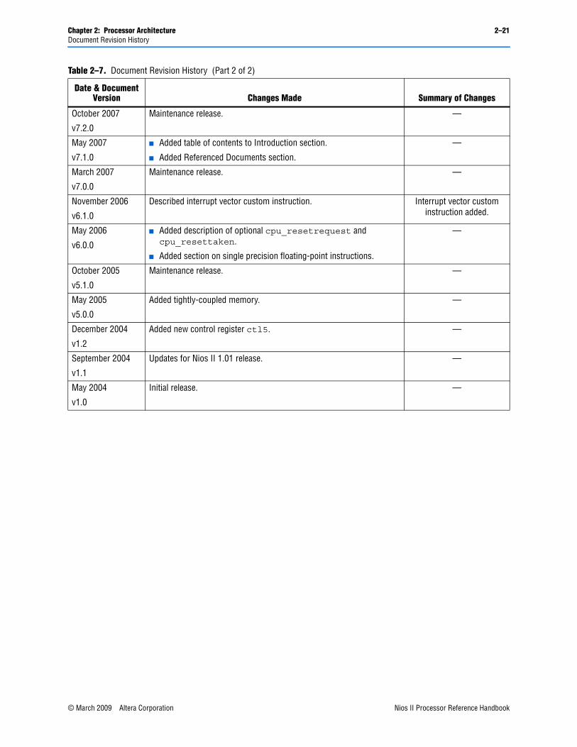
Chapter 2: Processor Architecture 2–21Document Revision History
October 2007
v7.2.0
Maintenance release. —
May 2007
v7.1.0
■ Added table of contents to Introduction section.
■ Added Referenced Documents section.
—
March 2007
v7.0.0
Maintenance release. —
November 2006
v6.1.0
Described interrupt vector custom instruction. Interrupt vector custom instruction added.
May 2006
v6.0.0
■ Added description of optional cpu_resetrequest and cpu_resettaken.
■ Added section on single precision floating-point instructions.
—
October 2005
v5.1.0
Maintenance release. —
May 2005
v5.0.0
Added tightly-coupled memory. —
December 2004
v1.2
Added new control register ctl5. —
September 2004
v1.1
Updates for Nios II 1.01 release. —
May 2004
v1.0
Initial release. —
Table 2–7. Document Revision History (Part 2 of 2)
Date & Document Version Changes Made Summary of Changes
© March 2009 Altera Corporation Nios II Processor Reference HandbookPreliminary

2–22 Chapter 2: Processor ArchitectureDocument Revision History
Nios II Processor Reference Handbook © March 2009 Altera CorporationPreliminary

© March 2009 Altera Corporation
NII51003-9.0.0
3. Programming Model
IntroductionThis chapter describes the Nios® II programming model, covering processor features at the assembly language level. Fully understanding the contents of this chapter requires prior knowledge of computer architecture, operating systems, virtual memory and memory management, software processes and process management, exception handling, and instruction sets. This chapter assumes you have a detailed understanding of the aforementioned concepts and focuses on how these concepts are specifically implemented in the Nios II processor. Where possible, this chapter uses industry-standard terminology.
This chapter discusses the following topics from the system programmer’s perspective:
■ Operating modes, page 3–2—Defines the relationships between executable code and memory.
■ Memory management unit (MMU), page 3–3—Describes virtual memory support for full-featured operating systems.
■ Memory protection unit (MPU), page 3–8—Describes memory protection without virtual memory management.
■ General-purpose registers, page 3–10—Describes the Nios II general register set.
■ Control registers, page 3–11—Describes the Nios II control register set.
■ Exception processing, page 3–25—Describes how the Nios II processor responds to exceptions.
■ Processor reset state, page 3–27—Describes how the Nios II processor responds to a processor reset signal.
■ Hardware-assisted debug processing, page 3–28—Describes how the Nios II processor responds to break exceptions.
■ Hardware interrupts, page 3–29—Describes how the Nios II processor responds to hardware interrupts.
■ Memory, cache memory, and peripheral organization, page 3–38—Describes how the Nios II processor interfaces with memory and peripherals.
■ Instruction set categories, page 3–40—Introduces the Nios II instruction set.
■ Custom instructions, page 3–44—Describes the scope of Nios II custom instructions.
1 Because of the flexibility and capability range of the Nios II processor, this chapter covers topics that support a variety of operating systems and runtime environments. While reading, be aware that all sections might not apply to you. For example, if you are using a minimal system runtime environment, you can skip the sections covering operating modes, the MMU, the MPU, or the control registers exclusively used by the MMU and MPU.
Nios II Processor Reference HandbookPreliminary
3–2 Chapter 3: Programming ModelOperating Modes
f High-level software development tools are not discussed here. Refer to the Nios II Software Developer’s Handbook for information about developing software.
Operating ModesOperating modes control how the processor operates, manages system memory, and accesses peripherals. The Nios II architecture supports these operating modes:
■ Supervisor mode
■ User mode
The following sections define the modes, their relationship to your system software and application code, and their relationship to the Nios II MMU and Nios II MPU. Refer to “Memory Management Unit” on page 3–3 for more information about the Nios II MMU. Refer to “Memory Protection Unit” on page 3–8 for more information about the Nios II MPU.
Supervisor ModeSupervisor mode allows unrestricted operation of the processor. All code has access to all processor instructions and resources. The processor may perform any operation the Nios II architecture provides. Any instruction may be executed, any I/O operation may be initiated, and any area of memory may be accessed.
Operating systems and other system software run in supervisor mode. In systems with an MMU, application code runs in user mode, and the operating system, running in supervisor mode, controls the application’s access to memory and peripherals. In systems with an MPU, your system software controls the mode in which your application code runs. In Nios II systems without an MMU or MPU, all application and system code runs in supervisor mode.
Code that needs direct access to and control of the processor runs in supervisor mode. For example, the processor enters supervisor mode whenever a processor exception (including processor reset or break) occurs. Software debugging tools also use supervisor mode to implement features such as breakpoints and watchpoints.
1 For systems without an MMU or MPU, all code runs in supervisor mode.
User ModeUser mode is available only when the Nios II processor in your hardware design includes an MMU or MPU. User mode exists solely to support operating systems. Operating systems (that make use of the processor’s user mode) run your application code in user mode. The user mode capabilities of the processor are a subset of the supervisor mode capabilities. Only a subset of the instruction set is available in user mode.
The operating system determines which memory addresses are accessible to user mode applications. Attempts by user mode applications to access memory locations without user access enabled are not permitted and cause an exception. Code running in user mode uses system calls to make requests to the operating system to perform I/O operations, manage memory, and access other system functionality in the supervisor memory.
Nios II Processor Reference Handbook © March 2009 Altera CorporationPreliminary
Chapter 3: Programming Model 3–3Memory Management Unit
The Nios II MMU statically divides the 32-bit virtual address space into user and supervisor partitions. Refer to “Address Space and Memory Partitions” on page 3–4 for more information about the MMU memory partitions. The MMU provides operating systems access permissions on a per-page basis. Refer to “Virtual Addressing” on page 3–3 for more information about MMU pages.
The Nios II MPU supervisor and user memory divisions are determined by the operating system or runtime environment. The MPU provides user access permissions on a region basis. Refer to “Memory Regions” on page 3–8 for more information about MPU regions.
Memory Management UnitThe Nios II processor provides an MMU to support full-featured operating systems. Operating systems that require virtual memory rely on an MMU to manage the virtual memory. When present, the MMU manages memory accesses including translation of virtual addresses to physical addresses, memory protection, cache control, and software process memory allocation.
Recommended UsageIncluding the Nios II MMU in your Nios II hardware system is optional. The MMU is only useful with an operating system that takes advantage of it.
Many Nios II systems have simpler requirements where minimal system software or a small-footprint operating system (such as Altera® HAL or a third party real-time operating system) is sufficient. Such software is unlikely to function correctly in a hardware system with an MMU-based Nios II processor. Do not include an MMU in your Nios II system unless your operating system requires it.
1 The Altera HAL and HAL-based real-time operating systems do not support the MMU.
If your system needs memory protection, but not virtual memory management, refer to “Memory Protection Unit” on page 3–8.
Memory ManagementMemory management comprises two key functions:
■ Virtual addressing—Mapping a virtual memory space into a physical memory space
■ Memory protection—Allowing access only to certain memory under certain conditions
Virtual AddressingA virtual address is the address that software uses. A physical address is the address which the hardware outputs on the address lines of the Avalon® bus. The Nios II MMU divides virtual memory into 4 KByte pages and physical memory into 4 KByte frames.
© March 2009 Altera Corporation Nios II Processor Reference HandbookPreliminary
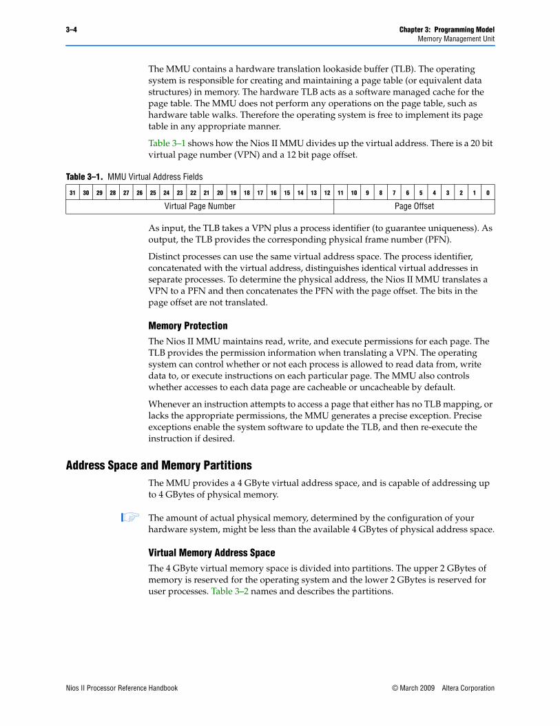
3–4 Chapter 3: Programming ModelMemory Management Unit
The MMU contains a hardware translation lookaside buffer (TLB). The operating system is responsible for creating and maintaining a page table (or equivalent data structures) in memory. The hardware TLB acts as a software managed cache for the page table. The MMU does not perform any operations on the page table, such as hardware table walks. Therefore the operating system is free to implement its page table in any appropriate manner.
Table 3–1 shows how the Nios II MMU divides up the virtual address. There is a 20 bit virtual page number (VPN) and a 12 bit page offset.
As input, the TLB takes a VPN plus a process identifier (to guarantee uniqueness). As output, the TLB provides the corresponding physical frame number (PFN).
Distinct processes can use the same virtual address space. The process identifier, concatenated with the virtual address, distinguishes identical virtual addresses in separate processes. To determine the physical address, the Nios II MMU translates a VPN to a PFN and then concatenates the PFN with the page offset. The bits in the page offset are not translated.
Memory ProtectionThe Nios II MMU maintains read, write, and execute permissions for each page. The TLB provides the permission information when translating a VPN. The operating system can control whether or not each process is allowed to read data from, write data to, or execute instructions on each particular page. The MMU also controls whether accesses to each data page are cacheable or uncacheable by default.
Whenever an instruction attempts to access a page that either has no TLB mapping, or lacks the appropriate permissions, the MMU generates a precise exception. Precise exceptions enable the system software to update the TLB, and then re-execute the instruction if desired.
Address Space and Memory PartitionsThe MMU provides a 4 GByte virtual address space, and is capable of addressing up to 4 GBytes of physical memory.
1 The amount of actual physical memory, determined by the configuration of your hardware system, might be less than the available 4 GBytes of physical address space.
Virtual Memory Address SpaceThe 4 GByte virtual memory space is divided into partitions. The upper 2 GBytes of memory is reserved for the operating system and the lower 2 GBytes is reserved for user processes. Table 3–2 names and describes the partitions.
Table 3–1. MMU Virtual Address Fields
31 30 29 28 27 26 25 24 23 22 21 20 19 18 17 16 15 14 13 12 11 10 9 8 7 6 5 4 3 2 1 0
Virtual Page Number Page Offset
Nios II Processor Reference Handbook © March 2009 Altera CorporationPreliminary
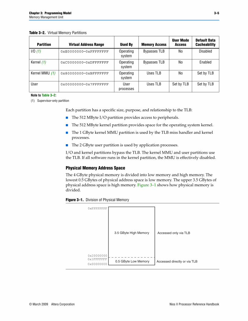
Chapter 3: Programming Model 3–5Memory Management Unit
Each partition has a specific size, purpose, and relationship to the TLB:
■ The 512 MByte I/O partition provides access to peripherals.
■ The 512 MByte kernel partition provides space for the operating system kernel.
■ The 1 GByte kernel MMU partition is used by the TLB miss handler and kernel processes.
■ The 2 GByte user partition is used by application processes.
I/O and kernel partitions bypass the TLB. The kernel MMU and user partitions use the TLB. If all software runs in the kernel partition, the MMU is effectively disabled.
Physical Memory Address SpaceThe 4 GByte physical memory is divided into low memory and high memory. The lowest 0.5 GBytes of physical address space is low memory. The upper 3.5 GBytes of physical address space is high memory. Figure 3–1 shows how physical memory is divided.
Table 3–2. Virtual Memory Partitions
Partition Virtual Address Range Used By Memory AccessUser Mode
AccessDefault Data Cacheability
I/O (1) 0xE0000000–0xFFFFFFFF Operating system
Bypasses TLB No Disabled
Kernel (1) 0xC0000000–0xDFFFFFFF Operating system
Bypasses TLB No Enabled
Kernel MMU (1) 0x80000000–0xBFFFFFFF Operating system
Uses TLB No Set by TLB
User 0x00000000–0x7FFFFFFF User processes
Uses TLB Set by TLB Set by TLB
Note to Table 3–2:
(1) Supervisor-only partition
Figure 3–1. Division of Physical Memory
0x1FFFFFFF
0x000000000.5 GByte Low Memory
3.5 GByte High Memory
0xFFFFFFFF
0x20000000
Accessed directly or via TLB
Accessed only via TLB
© March 2009 Altera Corporation Nios II Processor Reference HandbookPreliminary

3–6 Chapter 3: Programming ModelMemory Management Unit
High physical memory can only be accessed through the TLB. Any physical address in low memory (29-bits or less) can be accessed through the TLB or by bypassing the TLB. When bypassing the TLB, a 29-bit physical address is computed by clearing the top three bits of the 32-bit virtual address.
1 To function correctly, the base physical address of all exception vectors (reset, general exception, break, and fast TLB miss) must point to low physical memory so that hardware can correctly map their virtual addresses into the kernel partition. This restriction is enforced by the Nios II Processor MegaWizard interface in SOPC Builder.
Data CacheabilityEach partition has a rule that determines the default data cacheability property of each memory access. When data cacheability is enabled on a partition of the address space, a data access to that partition can be cached, if a data cache is present in the system. When data cacheability is disabled, all access to that partition goes directly to the Avalon switch fabric. Bit 31 is not used to specify data cacheability, as it is in Nios II cores without MMUs. Virtual memory partitions that bypass the TLB have a default data cacheability property, as shown in Table 3–2. For partitions that are mapped through the TLB, data cacheability is controlled by the TLB on a per-page basis.
Non-I/O load and store instructions use the default data cacheability property. I/O load and store instructions are always non-cacheable, so they ignore the default data cacheability property.
TLB OrganizationA TLB functions as a cache for the operating system’s page table. In Nios II processors with an MMU, one main TLB is shared by instruction and data accesses. The TLB is stored in on-chip RAM and handles translations for instruction fetches and instructions that perform data accesses.
The TLB is organized as an n-way set-associative cache. The software specifies the way (set) when loading a new entry.
1 You can configure the number of TLB entries and the number of ways (set associativity) of the TLB in SOPC Builder at system generation time. By default, the TLB is a 16-way cache. The default number of entries depends on the target device, as follows:
■ Cyclone®, Cyclone II, Stratix®, Stratix II, Stratix II GX—128 entries, requiring one M4K RAM
■ Cyclone III, Stratix III, Stratix IV—256 entries, requiring one M9K RAM
For further detail, refer to the Instantiating the Nios II Processor in SOPC Builder chapter of the Nios II Processor Reference Handbook.
The operating system software is responsible for guaranteeing that multiple TLB entries do not map the same virtual address. The hardware behavior is undefined when multiple entries map the same virtual address.
Each TLB entry consists of a tag and data portion. This is analogous to the tag and data portion of instruction and data caches.
Nios II Processor Reference Handbook © March 2009 Altera CorporationPreliminary
Chapter 3: Programming Model 3–7Memory Management Unit
f Refer to the Nios II Core Implementation Details chapter of the Nios II Processor Reference Handbook for details on instruction and data caches.
The tag portion of a TLB entry contains information used when matching a virtual address to a TLB entry. Table 3–3 describes the tag portion of a TLB entry.
The TLB data portion determines how to translate a matching virtual address to a physical address. Table 3–4 describes the data portion of a TLB entry.
1 Because there is no “valid bit” in the TLB entry, the operating system software invalidates the TLB by writing unique VPN values from the I/O partition of virtual addresses into each TLB entry.
TLB LookupsA TLB lookup attempts to convert a virtual address (VADDR) to a physical address (PADDR).
The TLB lookup algorithm for instruction fetches is as follows:
if (VPN match and (G = 1 or PID match)) if (X = 1)
PADDR = concat(PFN, VADDR[11:0]) else
take TLB permission violation exception else
if (EH bit of status register = 1) take double TLB miss exception
else take fast TLB miss exception
Refer to “Instruction-Related Exceptions” on page 3–30 for details on TLB exceptions.
Table 3–3. TLB Tag Portion Contents
Field Name Description
VPN VPN is the virtual page number field. This field is compared with the top 20 bits of the virtual address.
PID PID is the process identifier field. This field is compared with the value of the current process identifier stored in the tlbmisc control register, effectively extending the virtual address. The field size is configurable at system generation time, and can be between 8 and 14 bits.
G G is the global flag. When G = 1, the PID is ignored in the TLB lookup.
Table 3–4. TLB Data Portion Contents
Field Name Description
PFN PFN is the physical frame number field. This field specifies the upper bits of the physical address. The size of this field depends on the range of physical addresses present in the system. The maximum size is 20 bits.
C C is the cacheable flag. Determines the default data cacheability of a page. Can be overridden for data accesses using I/O load and store family of Nios II instructions.
R R is the readable flag. Allows load instructions to read a page.
W W is the writeable flag. Allows store instructions to write a page.
X X is the executable flag. Allows instruction fetches from a page.
© March 2009 Altera Corporation Nios II Processor Reference HandbookPreliminary
3–8 Chapter 3: Programming ModelMemory Protection Unit
The TLB lookup algorithm for data accesses is as follows:
if (VPN match and (G = 1 or PID match)) if ((load and R = 1) or (store and W = 1) or flushda)
PADDR = concatenate(PFN, VADDR[11:0]) else
take TLB permission violation exception else
if (EH bit of status register = 1) take double TLB miss exception
else take fast TLB miss exception
Memory Protection UnitThe Nios II processor provides an MPU for operating systems and runtime environments that desire memory protection but do not require virtual memory management. For information about memory protection with virtual memory management, refer to “Memory Management Unit” on page 3–3.
When present and enabled, the MPU monitors all Nios II instruction fetches and data memory accesses to protect against errant software execution. The MPU is a hardware facility that system software uses to define memory regions and their associated access permissions. The MPU triggers a precise exception if software attempts to access a memory region in violation of its permissions, allowing you to intervene and handle the exception as appropriate. The precise exception effectively prevents the illegal access to memory.
The MPU extends the Nios II processor to support user mode and supervisor mode. Typically, system software runs in supervisor mode and end-user applications run in user mode, although all software can run in supervisor mode if desired. System software defines which MPU regions belong to supervisor mode and which belong to user mode.
Memory RegionsThe MPU contains up to 32 instruction regions and 32 data regions. Each region is defined by the following attributes:
■ Base address
■ Region type
■ Region index
■ Region size or upper address limit
■ Access permissions
■ Default cacheability (data regions only)
Base AddressThe base address specifies the lowest address of the region. The base address is aligned on a region-sized boundary. For example, a 4 Kbyte region must have a base address that is a multiple of 4 Kbytes. If the base address is not properly aligned, the behavior is undefined.
Nios II Processor Reference Handbook © March 2009 Altera CorporationPreliminary
Chapter 3: Programming Model 3–9Memory Protection Unit
Region TypeEach region is identified as either an instruction region or a data region.
Region IndexEach region has an index ranging from zero to the number of regions of its region type minus one. Index zero has the highest priority.
Region Size or Upper Address LimitAn SOPC Builder generation-time option controls whether the amount of memory in the region is defined by size or upper address limit. The size is an integer power of two bytes. The limit is the highest address of the region plus one. The minimum supported region size is 64 bytes but can be configured at system generation time for larger minimum sizes to save logic resources. The maximum supported region size equals the Nios II address space (a function of the address ranges of slaves connected to the Nios II masters). Any access outside of the Nios II address space is considered not to match any region and triggers an MPU region violation exception.
When regions are defined by size, the size is encoded as a binary mask to facilitate the following MPU region address range matching:
(address & region_mask) == region_base_address
When regions are defined by limit, the limit is encoded as an unsigned integer to facilitate the following MPU region address range matching:
(address >= region_base) && (address < region_limit)
The region limit uses a less-than instead of a less-than-or-equal-to comparison because less-than provides a more efficient implementation. The limit is one bit larger than the address so that full address range may be included in a range. Defining the region by limit results in slower and larger address range match logic than defining by size but allows finer granularity in region sizes.
Access PermissionsThe access permissions consist of execute permissions for instruction regions and read/write permissions for data regions. Any instruction that performs a memory access that violates the access permissions triggers an exception. Additionally, any instruction that performs a memory access that does not match any region triggers an exception.
Default CacheabilityThe default cacheability specifies whether normal load and store instructions access the data cache or bypass the data cache. The default cacheability is only present for data regions. You can override the default cacheability by using the ldio or stio instructions. The bit 31 cache bypass feature is available when the MPU is present. Refer to “Cache Memory” on page 3–38 for more information on cache bypass.
© March 2009 Altera Corporation Nios II Processor Reference HandbookPreliminary
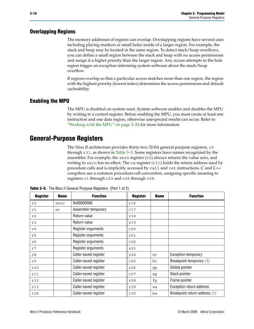
3–10 Chapter 3: Programming ModelGeneral-Purpose Registers
Overlapping RegionsThe memory addresses of regions can overlap. Overlapping regions have several uses including placing markers or small holes inside of a larger region. For example, the stack and heap may be located in the same region. To detect stack/heap overflows, you can define a small region between the stack and heap with no access permissions and assign it a higher priority than the larger region. Any access attempts to the hole region trigger an exception informing system software about the stack/heap overflow.
If regions overlap so that a particular access matches more than one region, the region with the highest priority (lowest index) determines the access permissions and default cacheability.
Enabling the MPUThe MPU is disabled on system reset. System software enables and disables the MPU by writing to a control register. Before enabling the MPU, you must create at least one instruction and one data region, otherwise unexpected results can occur. Refer to “Working with the MPU” on page 3–24 for more information.
General-Purpose RegistersThe Nios II architecture provides thirty-two 32-bit general-purpose registers, r0 through r31, as shown in Table 3–5. Some registers have names recognized by the assembler. For example, the zero register (r0) always returns the value zero, and writing to zero has no effect. The ra register (r31) holds the return address used by procedure calls and is implicitly accessed by call and ret instructions. C and C++ compilers use a common procedure-call convention, assigning specific meaning to registers r1 through r23 and r26 through r28.
Table 3–5. The Nios II General Purpose Registers (Part 1 of 2)
Register Name Function Register Name Function
r0 zero 0x00000000 r16
r1 at Assembler temporary r17
r2 Return value r18
r3 Return value r19
r4 Register arguments r20
r5 Register arguments r21
r6 Register arguments r22
r7 Register arguments r23
r8 Caller-saved register r24 et Exception temporary
r9 Caller-saved register r25 bt Breakpoint temporary (1)
r10 Caller-saved register r26 gp Global pointer
r11 Caller-saved register r27 sp Stack pointer
r12 Caller-saved register r28 fp Frame pointer
r13 Caller-saved register r29 ea Exception return address
r14 Caller-saved register r30 ba Breakpoint return address (1)
Nios II Processor Reference Handbook © March 2009 Altera CorporationPreliminary
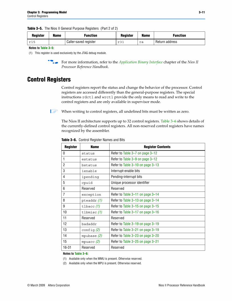
Chapter 3: Programming Model 3–11Control Registers
f For more information, refer to the Application Binary Interface chapter of the Nios II Processor Reference Handbook.
Control RegistersControl registers report the status and change the behavior of the processor. Control registers are accessed differently than the general-purpose registers. The special instructions rdctl and wrctl provide the only means to read and write to the control registers and are only available in supervisor mode.
1 When writing to control registers, all undefined bits must be written as zero.
The Nios II architecture supports up to 32 control registers. Table 3–6 shows details of the currently-defined control registers. All non-reserved control registers have names recognized by the assembler.
r15 Caller-saved register r31 ra Return address
Notes to Table 3–5:
(1) This register is used exclusively by the JTAG debug module.
Table 3–5. The Nios II General Purpose Registers (Part 2 of 2)
Register Name Function Register Name Function
Table 3–6. Control Register Names and Bits
Register Name Register Contents
0 status Refer to Table 3–7 on page 3–12
1 estatus Refer to Table 3–9 on page 3–12
2 bstatus Refer to Table 3–10 on page 3–13
3 ienable Interrupt-enable bits
4 ipending Pending-interrupt bits
5 cpuid Unique processor identifier
6 Reserved Reserved
7 exception Refer to Table 3–11 on page 3–14
8 pteaddr (1) Refer to Table 3–13 on page 3–14
9 tlbacc (1) Refer to Table 3–15 on page 3–15
10 tlbmisc (1) Refer to Table 3–17 on page 3–16
11 Reserved Reserved
12 badaddr Refer to Table 3–19 on page 3–19
13 config (2) Refer to Table 3–21 on page 3–19
14 mpubase (2) Refer to Table 3–23 on page 3–20
15 mpuacc (2) Refer to Table 3–25 on page 3–21
16-31 Reserved Reserved
Notes to Table 3–6:
(1) Available only when the MMU is present. Otherwise reserved.(2) Available only when the MPU is present. Otherwise reserved.
© March 2009 Altera Corporation Nios II Processor Reference HandbookPreliminary
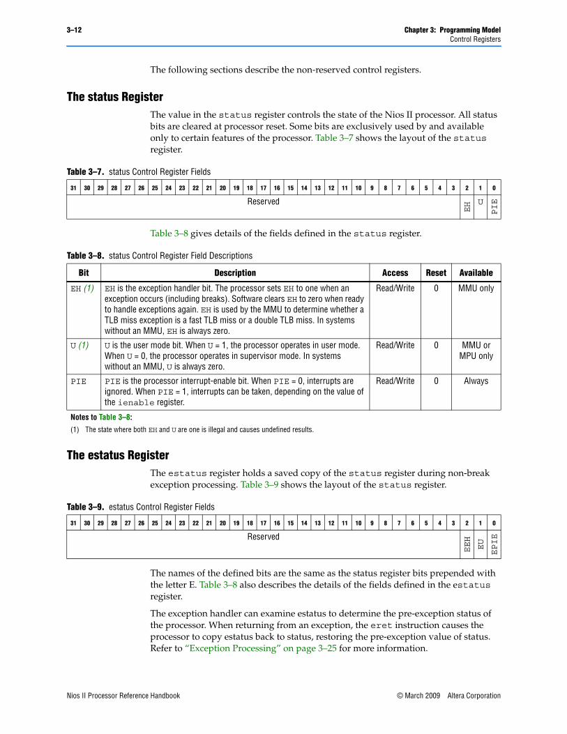
3–12 Chapter 3: Programming ModelControl Registers
The following sections describe the non-reserved control registers.
The status RegisterThe value in the status register controls the state of the Nios II processor. All status bits are cleared at processor reset. Some bits are exclusively used by and available only to certain features of the processor. Table 3–7 shows the layout of the status register.
Table 3–8 gives details of the fields defined in the status register.
The estatus RegisterThe estatus register holds a saved copy of the status register during non-break exception processing. Table 3–9 shows the layout of the status register.
The names of the defined bits are the same as the status register bits prepended with the letter E. Table 3–8 also describes the details of the fields defined in the estatus register.
The exception handler can examine estatus to determine the pre-exception status of the processor. When returning from an exception, the eret instruction causes the processor to copy estatus back to status, restoring the pre-exception value of status. Refer to “Exception Processing” on page 3–25 for more information.
Table 3–7. status Control Register Fields
31 30 29 28 27 26 25 24 23 22 21 20 19 18 17 16 15 14 13 12 11 10 9 8 7 6 5 4 3 2 1 0
Reserved
EH U
PIE
Table 3–8. status Control Register Field Descriptions
Bit Description Access Reset Available
EH (1) EH is the exception handler bit. The processor sets EH to one when an exception occurs (including breaks). Software clears EH to zero when ready to handle exceptions again. EH is used by the MMU to determine whether a TLB miss exception is a fast TLB miss or a double TLB miss. In systems without an MMU, EH is always zero.
Read/Write 0 MMU only
U (1) U is the user mode bit. When U = 1, the processor operates in user mode. When U = 0, the processor operates in supervisor mode. In systems without an MMU, U is always zero.
Read/Write 0 MMU or MPU only
PIE PIE is the processor interrupt-enable bit. When PIE = 0, interrupts are ignored. When PIE = 1, interrupts can be taken, depending on the value of the ienable register.
Read/Write 0 Always
Notes to Table 3–8:
(1) The state where both EH and U are one is illegal and causes undefined results.
Table 3–9. estatus Control Register Fields
31 30 29 28 27 26 25 24 23 22 21 20 19 18 17 16 15 14 13 12 11 10 9 8 7 6 5 4 3 2 1 0
Reserved
EEH
EU
EPIE
Nios II Processor Reference Handbook © March 2009 Altera CorporationPreliminary
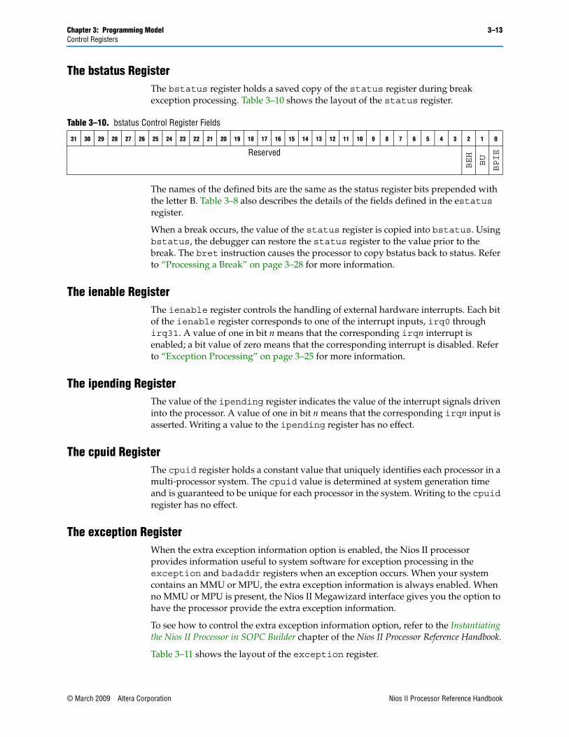
Chapter 3: Programming Model 3–13Control Registers
The bstatus RegisterThe bstatus register holds a saved copy of the status register during break exception processing. Table 3–10 shows the layout of the status register.
The names of the defined bits are the same as the status register bits prepended with the letter B. Table 3–8 also describes the details of the fields defined in the estatus register.
When a break occurs, the value of the status register is copied into bstatus. Using bstatus, the debugger can restore the status register to the value prior to the break. The bret instruction causes the processor to copy bstatus back to status. Refer to “Processing a Break” on page 3–28 for more information.
The ienable RegisterThe ienable register controls the handling of external hardware interrupts. Each bit of the ienable register corresponds to one of the interrupt inputs, irq0 through irq31. A value of one in bit n means that the corresponding irqn interrupt is enabled; a bit value of zero means that the corresponding interrupt is disabled. Refer to “Exception Processing” on page 3–25 for more information.
The ipending RegisterThe value of the ipending register indicates the value of the interrupt signals driven into the processor. A value of one in bit n means that the corresponding irqn input is asserted. Writing a value to the ipending register has no effect.
The cpuid RegisterThe cpuid register holds a constant value that uniquely identifies each processor in a multi-processor system. The cpuid value is determined at system generation time and is guaranteed to be unique for each processor in the system. Writing to the cpuid register has no effect.
The exception RegisterWhen the extra exception information option is enabled, the Nios II processor provides information useful to system software for exception processing in the exception and badaddr registers when an exception occurs. When your system contains an MMU or MPU, the extra exception information is always enabled. When no MMU or MPU is present, the Nios II Megawizard interface gives you the option to have the processor provide the extra exception information.
To see how to control the extra exception information option, refer to the Instantiating the Nios II Processor in SOPC Builder chapter of the Nios II Processor Reference Handbook.
Table 3–11 shows the layout of the exception register.
Table 3–10. bstatus Control Register Fields
31 30 29 28 27 26 25 24 23 22 21 20 19 18 17 16 15 14 13 12 11 10 9 8 7 6 5 4 3 2 1 0
Reserved
BEH
BU
BPIE
© March 2009 Altera Corporation Nios II Processor Reference HandbookPreliminary
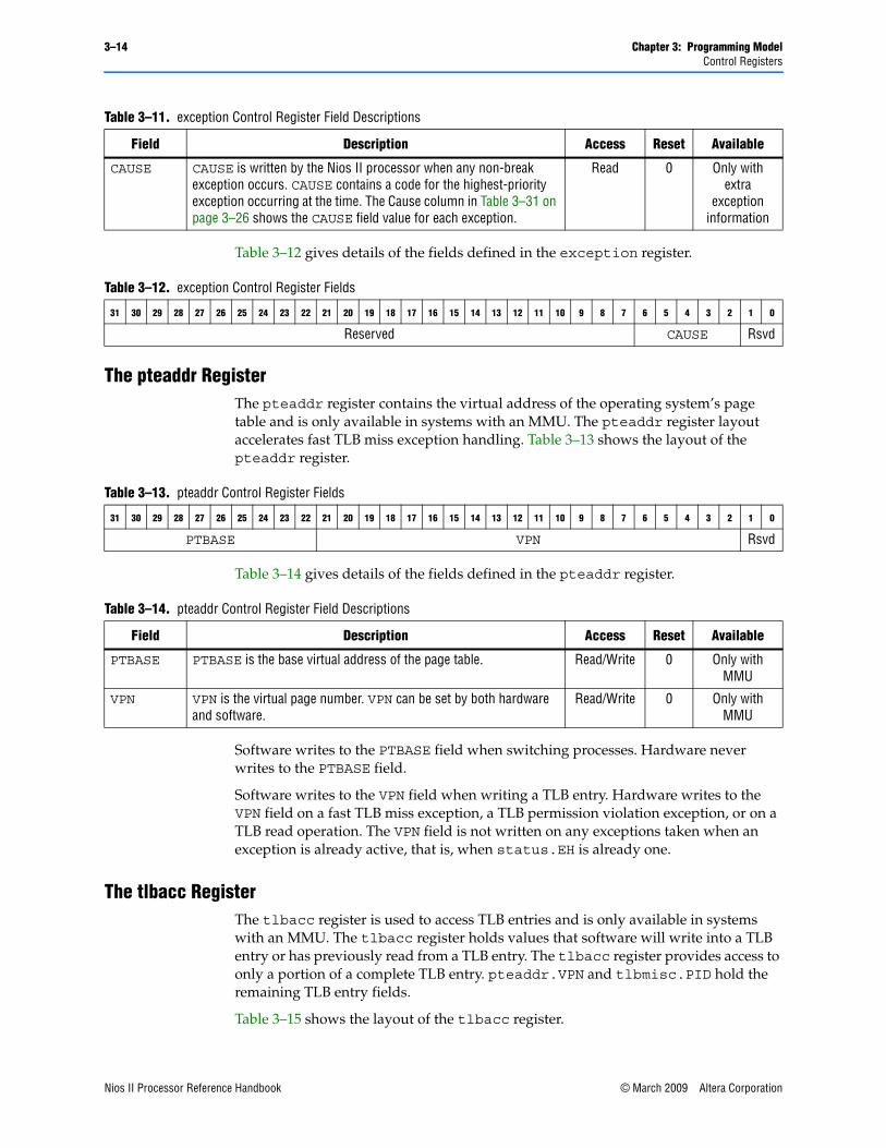
3–14 Chapter 3: Programming ModelControl Registers
Table 3–12 gives details of the fields defined in the exception register.
The pteaddr RegisterThe pteaddr register contains the virtual address of the operating system’s page table and is only available in systems with an MMU. The pteaddr register layout accelerates fast TLB miss exception handling. Table 3–13 shows the layout of the pteaddr register.
Table 3–14 gives details of the fields defined in the pteaddr register.
Software writes to the PTBASE field when switching processes. Hardware never writes to the PTBASE field.
Software writes to the VPN field when writing a TLB entry. Hardware writes to the VPN field on a fast TLB miss exception, a TLB permission violation exception, or on a TLB read operation. The VPN field is not written on any exceptions taken when an exception is already active, that is, when status.EH is already one.
The tlbacc RegisterThe tlbacc register is used to access TLB entries and is only available in systems with an MMU. The tlbacc register holds values that software will write into a TLB entry or has previously read from a TLB entry. The tlbacc register provides access to only a portion of a complete TLB entry. pteaddr.VPN and tlbmisc.PID hold the remaining TLB entry fields.
Table 3–15 shows the layout of the tlbacc register.
Table 3–11. exception Control Register Field Descriptions
Field Description Access Reset Available
CAUSE CAUSE is written by the Nios II processor when any non-break exception occurs. CAUSE contains a code for the highest-priority exception occurring at the time. The Cause column in Table 3–31 on page 3–26 shows the CAUSE field value for each exception.
Read 0 Only with extra
exception information
Table 3–12. exception Control Register Fields
31 30 29 28 27 26 25 24 23 22 21 20 19 18 17 16 15 14 13 12 11 10 9 8 7 6 5 4 3 2 1 0
Reserved CAUSE Rsvd
Table 3–13. pteaddr Control Register Fields
31 30 29 28 27 26 25 24 23 22 21 20 19 18 17 16 15 14 13 12 11 10 9 8 7 6 5 4 3 2 1 0
PTBASE VPN Rsvd
Table 3–14. pteaddr Control Register Field Descriptions
Field Description Access Reset Available
PTBASE PTBASE is the base virtual address of the page table. Read/Write 0 Only with MMU
VPN VPN is the virtual page number. VPN can be set by both hardware and software.
Read/Write 0 Only with MMU
Nios II Processor Reference Handbook © March 2009 Altera CorporationPreliminary
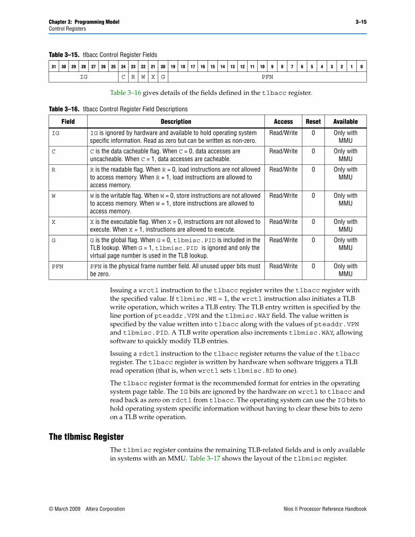
Chapter 3: Programming Model 3–15Control Registers
Table 3–16 gives details of the fields defined in the tlbacc register.
Issuing a wrctl instruction to the tlbacc register writes the tlbacc register with the specified value. If tlbmisc.WE = 1, the wrctl instruction also initiates a TLB write operation, which writes a TLB entry. The TLB entry written is specified by the line portion of pteaddr.VPN and the tlbmisc.WAY field. The value written is specified by the value written into tlbacc along with the values of pteaddr.VPN and tlbmisc.PID. A TLB write operation also increments tlbmisc.WAY, allowing software to quickly modify TLB entries.
Issuing a rdctl instruction to the tlbacc register returns the value of the tlbacc register. The tlbacc register is written by hardware when software triggers a TLB read operation (that is, when wrctl sets tlbmisc.RD to one).
The tlbacc register format is the recommended format for entries in the operating system page table. The IG bits are ignored by the hardware on wrctl to tlbacc and read back as zero on rdctl from tlbacc. The operating system can use the IG bits to hold operating system specific information without having to clear these bits to zero on a TLB write operation.
The tlbmisc RegisterThe tlbmisc register contains the remaining TLB-related fields and is only available in systems with an MMU. Table 3–17 shows the layout of the tlbmisc register.
Table 3–15. tlbacc Control Register Fields
31 30 29 28 27 26 25 24 23 22 21 20 19 18 17 16 15 14 13 12 11 10 9 8 7 6 5 4 3 2 1 0
IG C R W X G PFN
Table 3–16. tlbacc Control Register Field Descriptions
Field Description Access Reset Available
IG IG is ignored by hardware and available to hold operating system specific information. Read as zero but can be written as non-zero.
Read/Write 0 Only with MMU
C C is the data cacheable flag. When C = 0, data accesses are uncacheable. When C = 1, data accesses are cacheable.
Read/Write 0 Only with MMU
R R is the readable flag. When R = 0, load instructions are not allowed to access memory. When R = 1, load instructions are allowed to access memory.
Read/Write 0 Only with MMU
W W is the writable flag. When W = 0, store instructions are not allowed to access memory. When W = 1, store instructions are allowed to access memory.
Read/Write 0 Only with MMU
X X is the executable flag. When X = 0, instructions are not allowed to execute. When X = 1, instructions are allowed to execute.
Read/Write 0 Only with MMU
G G is the global flag. When G = 0, tlbmisc.PID is included in the TLB lookup. When G = 1, tlbmisc.PID is ignored and only the virtual page number is used in the TLB lookup.
Read/Write 0 Only with MMU
PFN PFN is the physical frame number field. All unused upper bits must be zero.
Read/Write 0 Only with MMU
© March 2009 Altera Corporation Nios II Processor Reference HandbookPreliminary
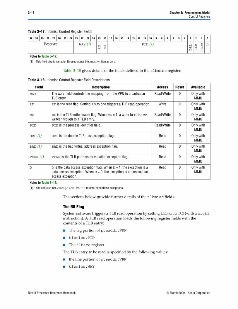
3–16 Chapter 3: Programming ModelControl Registers
Table 3–18 gives details of the fields defined in the tlbmisc register.
The sections below provide further details of the tlbmisc fields.
The RD FlagSystem software triggers a TLB read operation by setting tlbmisc.RD (with a wrctl instruction). A TLB read operation loads the following register fields with the contents of a TLB entry:
■ The tag portion of pteaddr.VPN
■ tlbmisc.PID
■ The tlbacc register
The TLB entry to be read is specified by the following values:
■ the line portion of pteaddr.VPN
■ tlbmisc.WAY
Table 3–17. tlbmisc Control Register Fields
31 30 29 28 27 26 25 24 23 22 21 20 19 18 17 16 15 14 13 12 11 10 9 8 7 6 5 4 3 2 1 0
Reserved WAY (1)
RD
WE
PID (1)
DBL
BAD
PERM D
Notes to Table 3–17:
(1) This field size is variable. Unused upper bits must written as zero.
Table 3–18. tlbmisc Control Register Field Descriptions
Field Description Access Reset Available
WAY The WAY field controls the mapping from the VPN to a particular TLB entry.
Read/Write 0 Only with MMU
RD RD is the read flag. Setting RD to one triggers a TLB read operation. Write 0 Only with MMU
WE WE is the TLB write enable flag. When WE = 1, a write to tlbacc writes through to a TLB entry.
Read/Write 0 Only with MMU
PID PID is the process identifier field. Read/Write 0 Only with MMU
DBL (1) DBL is the double TLB miss exception flag. Read 0 Only with MMU
BAD (1) BAD is the bad virtual address exception flag. Read 0 Only with MMU
PERM (1) PERM is the TLB permission violation exception flag. Read 0 Only with MMU
D D is the data access exception flag. When D = 1, the exception is a data access exception. When D = 0, the exception is an instruction access exception.
Read 0 Only with MMU
Notes to Table 3–18:
(1) You can also use exception.CAUSE to determine these exceptions.
Nios II Processor Reference Handbook © March 2009 Altera CorporationPreliminary
Chapter 3: Programming Model 3–17Control Registers
When system software changes the fields that specify the TLB entry, there is no immediate effect on pteaddr.VPN, tlbmisc.PID, or the tlbacc register. The registers retain their previous values until the next TLB read operation is initiated. For example, when the operating system sets pteaddr.VPN to a new value, the contents of tlbacc continues to reflect the previous TLB entry. tlbacc does not contain the new TLB entry until after an explicit TLB read.
The WE FlagWhen WE = 1, a write to tlbacc writes the tlbacc register and a TLB entry. When WE = 0, a write to tlbacc only writes the tlbacc register.
Hardware sets the WE flag to one on a TLB permission violation exception, and on a TLB miss exception when status.EH = 0. When a TLB write operation writes the tlbacc register, the write operation also writes to a TLB entry when WE = 1.
The WAY FieldThe WAY field controls the mapping from the VPN to a particular TLB entry. WAY specifies the set to be written to in the TLB. The MMU increments WAY when system software performs a TLB write operation. Unused upper bits in WAY must be written as zero.
1 The number of ways (sets) is configurable in SOPC Builder at generation time, up to a maximum of 16.
The PID FieldPID is a unique identifier for the current process that effectively extends the virtual address. The process identifier can be less than 14 bits. Any unused upper bits must be zero.
tlbmisc.PID contains the PID field from a TLB tag. The operating system must set the PID field when switching processes, and before each TLB write operation.
1 Use of the process identifier is optional. To implement memory management without process identifiers, clear tlbmisc.PID to zero. Without a process identifier, all processes share the same virtual address space.
The MMU sets tlbmisc.PID on a TLB read operation. When the software triggers a TLB read, by setting tlbmisc.RD to one with the wrctl instruction, the PID value read from the TLB has priority over the value written by the wrctl instruction.
The size of the PID field is configured in SOPC Builder at system generation, and can be from 8 to 14 bits. If system software defines a process identifier smaller than the PID field, unused upper bits must be written as zero.
The DBL FlagDuring a general exception, the processor sets DBL to one when a double TLB miss condition exists. Otherwise, the processor clears DBL to zero.
The DBL flag indicates whether the most recent exception is a double TLB miss condition. When a general exception occurs, the MMU sets DBL to one if a double TLB miss is detected, and clears DBL to zero otherwise.
© March 2009 Altera Corporation Nios II Processor Reference HandbookPreliminary
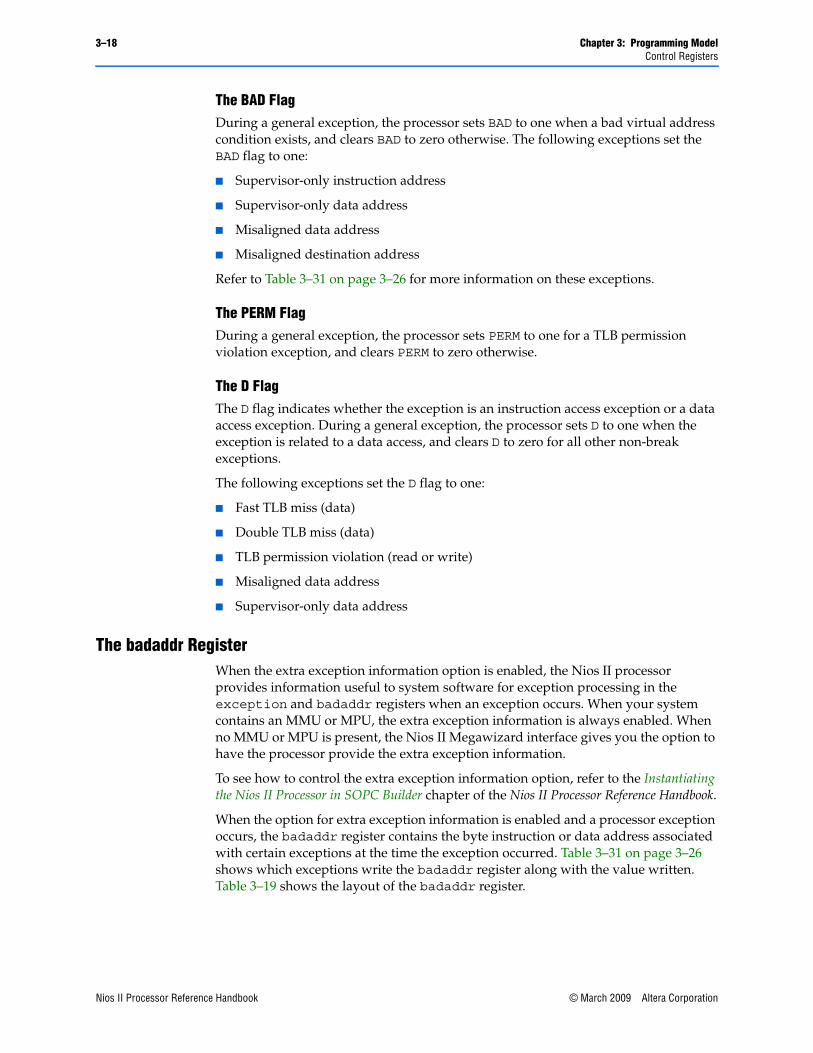
3–18 Chapter 3: Programming ModelControl Registers
The BAD FlagDuring a general exception, the processor sets BAD to one when a bad virtual address condition exists, and clears BAD to zero otherwise. The following exceptions set the BAD flag to one:
■ Supervisor-only instruction address
■ Supervisor-only data address
■ Misaligned data address
■ Misaligned destination address
Refer to Table 3–31 on page 3–26 for more information on these exceptions.
The PERM FlagDuring a general exception, the processor sets PERM to one for a TLB permission violation exception, and clears PERM to zero otherwise.
The D FlagThe D flag indicates whether the exception is an instruction access exception or a data access exception. During a general exception, the processor sets D to one when the exception is related to a data access, and clears D to zero for all other non-break exceptions.
The following exceptions set the D flag to one:
■ Fast TLB miss (data)
■ Double TLB miss (data)
■ TLB permission violation (read or write)
■ Misaligned data address
■ Supervisor-only data address
The badaddr RegisterWhen the extra exception information option is enabled, the Nios II processor provides information useful to system software for exception processing in the exception and badaddr registers when an exception occurs. When your system contains an MMU or MPU, the extra exception information is always enabled. When no MMU or MPU is present, the Nios II Megawizard interface gives you the option to have the processor provide the extra exception information.
To see how to control the extra exception information option, refer to the Instantiating the Nios II Processor in SOPC Builder chapter of the Nios II Processor Reference Handbook.
When the option for extra exception information is enabled and a processor exception occurs, the badaddr register contains the byte instruction or data address associated with certain exceptions at the time the exception occurred. Table 3–31 on page 3–26 shows which exceptions write the badaddr register along with the value written. Table 3–19 shows the layout of the badaddr register.
Nios II Processor Reference Handbook © March 2009 Altera CorporationPreliminary
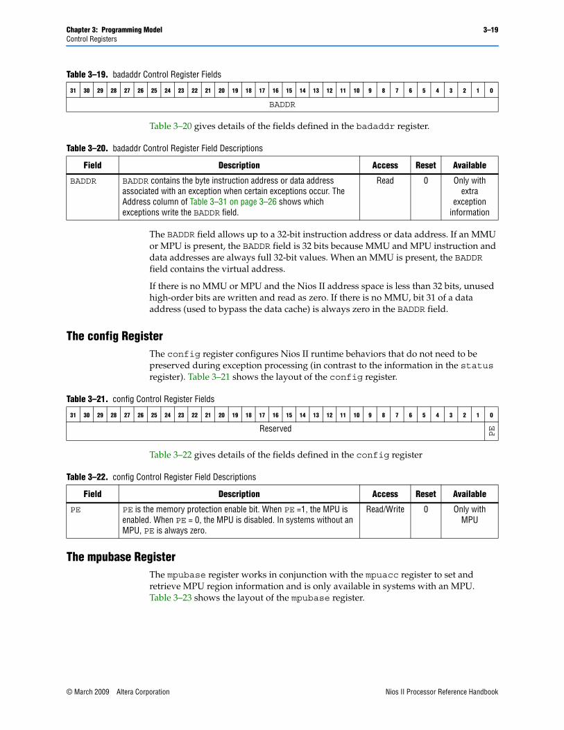
Chapter 3: Programming Model 3–19Control Registers
Table 3–20 gives details of the fields defined in the badaddr register.
The BADDR field allows up to a 32-bit instruction address or data address. If an MMU or MPU is present, the BADDR field is 32 bits because MMU and MPU instruction and data addresses are always full 32-bit values. When an MMU is present, the BADDR field contains the virtual address.
If there is no MMU or MPU and the Nios II address space is less than 32 bits, unused high-order bits are written and read as zero. If there is no MMU, bit 31 of a data address (used to bypass the data cache) is always zero in the BADDR field.
The config RegisterThe config register configures Nios II runtime behaviors that do not need to be preserved during exception processing (in contrast to the information in the status register). Table 3–21 shows the layout of the config register.
Table 3–22 gives details of the fields defined in the config register
The mpubase RegisterThe mpubase register works in conjunction with the mpuacc register to set and retrieve MPU region information and is only available in systems with an MPU. Table 3–23 shows the layout of the mpubase register.
Table 3–19. badaddr Control Register Fields
31 30 29 28 27 26 25 24 23 22 21 20 19 18 17 16 15 14 13 12 11 10 9 8 7 6 5 4 3 2 1 0
BADDR
Table 3–20. badaddr Control Register Field Descriptions
Field Description Access Reset Available
BADDR BADDR contains the byte instruction address or data address associated with an exception when certain exceptions occur. The Address column of Table 3–31 on page 3–26 shows which exceptions write the BADDR field.
Read 0 Only with extra
exception information
Table 3–21. config Control Register Fields
31 30 29 28 27 26 25 24 23 22 21 20 19 18 17 16 15 14 13 12 11 10 9 8 7 6 5 4 3 2 1 0
Reserved
PE
Table 3–22. config Control Register Field Descriptions
Field Description Access Reset Available
PE PE is the memory protection enable bit. When PE =1, the MPU is enabled. When PE = 0, the MPU is disabled. In systems without an MPU, PE is always zero.
Read/Write 0 Only with MPU
© March 2009 Altera Corporation Nios II Processor Reference HandbookPreliminary
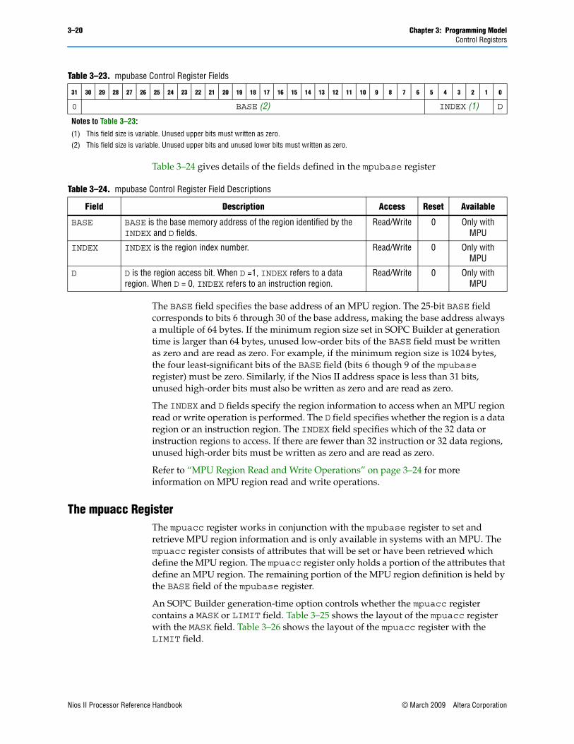
3–20 Chapter 3: Programming ModelControl Registers
Table 3–24 gives details of the fields defined in the mpubase register.
The BASE field specifies the base address of an MPU region. The 25-bit BASE field corresponds to bits 6 through 30 of the base address, making the base address always a multiple of 64 bytes. If the minimum region size set in SOPC Builder at generation time is larger than 64 bytes, unused low-order bits of the BASE field must be written as zero and are read as zero. For example, if the minimum region size is 1024 bytes, the four least-significant bits of the BASE field (bits 6 though 9 of the mpubase register) must be zero. Similarly, if the Nios II address space is less than 31 bits, unused high-order bits must also be written as zero and are read as zero.
The INDEX and D fields specify the region information to access when an MPU region read or write operation is performed. The D field specifies whether the region is a data region or an instruction region. The INDEX field specifies which of the 32 data or instruction regions to access. If there are fewer than 32 instruction or 32 data regions, unused high-order bits must be written as zero and are read as zero.
Refer to “MPU Region Read and Write Operations” on page 3–24 for more information on MPU region read and write operations.
The mpuacc RegisterThe mpuacc register works in conjunction with the mpubase register to set and retrieve MPU region information and is only available in systems with an MPU. The mpuacc register consists of attributes that will be set or have been retrieved which define the MPU region. The mpuacc register only holds a portion of the attributes that define an MPU region. The remaining portion of the MPU region definition is held by the BASE field of the mpubase register.
An SOPC Builder generation-time option controls whether the mpuacc register contains a MASK or LIMIT field. Table 3–25 shows the layout of the mpuacc register with the MASK field. Table 3–26 shows the layout of the mpuacc register with the LIMIT field.
Table 3–23. mpubase Control Register Fields
31 30 29 28 27 26 25 24 23 22 21 20 19 18 17 16 15 14 13 12 11 10 9 8 7 6 5 4 3 2 1 0
0 BASE (2) INDEX (1) D
Notes to Table 3–23:
(1) This field size is variable. Unused upper bits must written as zero.(2) This field size is variable. Unused upper bits and unused lower bits must written as zero.
Table 3–24. mpubase Control Register Field Descriptions
Field Description Access Reset Available
BASE BASE is the base memory address of the region identified by the INDEX and D fields.
Read/Write 0 Only with MPU
INDEX INDEX is the region index number. Read/Write 0 Only with MPU
D D is the region access bit. When D =1, INDEX refers to a data region. When D = 0, INDEX refers to an instruction region.
Read/Write 0 Only with MPU
Nios II Processor Reference Handbook © March 2009 Altera CorporationPreliminary
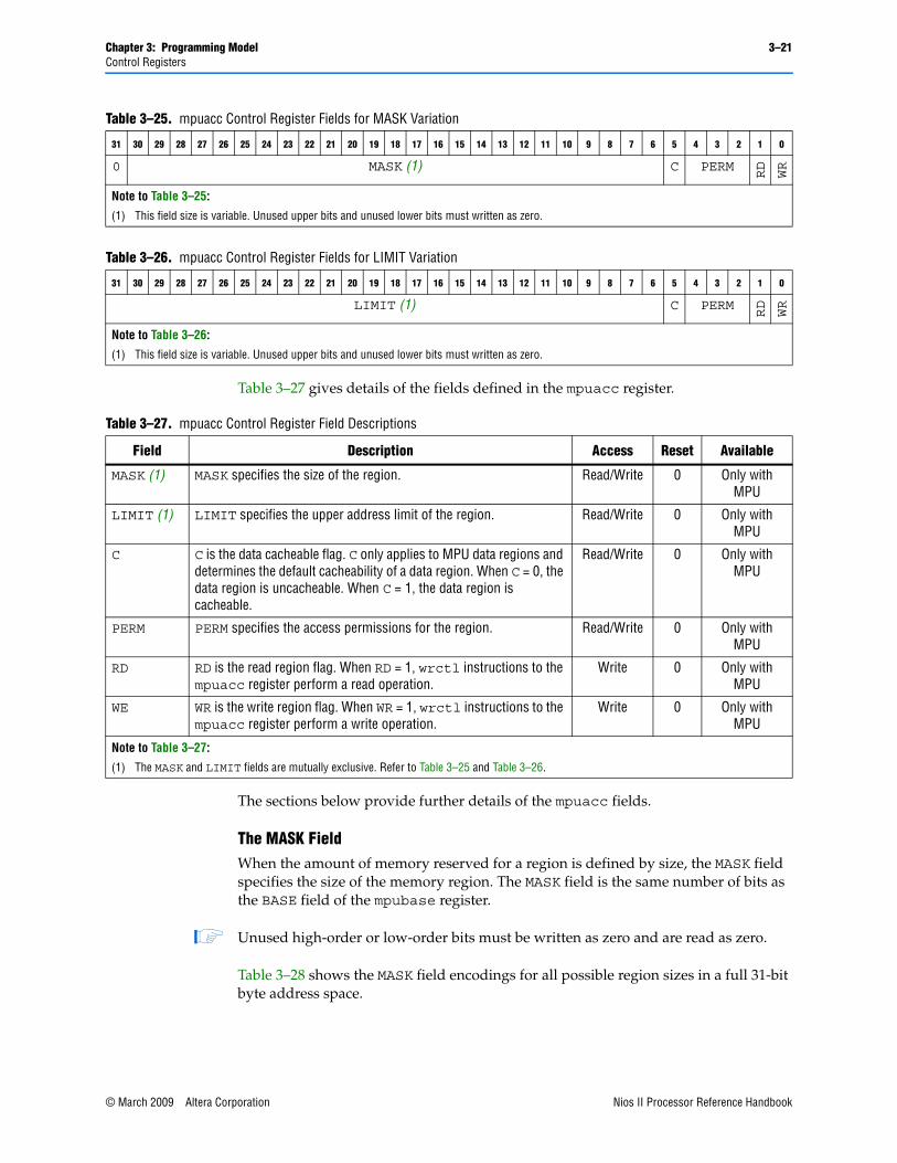
Chapter 3: Programming Model 3–21Control Registers
Table 3–27 gives details of the fields defined in the mpuacc register.
The sections below provide further details of the mpuacc fields.
The MASK FieldWhen the amount of memory reserved for a region is defined by size, the MASK field specifies the size of the memory region. The MASK field is the same number of bits as the BASE field of the mpubase register.
1 Unused high-order or low-order bits must be written as zero and are read as zero.
Table 3–28 shows the MASK field encodings for all possible region sizes in a full 31-bit byte address space.
Table 3–25. mpuacc Control Register Fields for MASK Variation
31 30 29 28 27 26 25 24 23 22 21 20 19 18 17 16 15 14 13 12 11 10 9 8 7 6 5 4 3 2 1 0
0 MASK (1) C PERM
RD
WR
Note to Table 3–25:
(1) This field size is variable. Unused upper bits and unused lower bits must written as zero.
Table 3–26. mpuacc Control Register Fields for LIMIT Variation
31 30 29 28 27 26 25 24 23 22 21 20 19 18 17 16 15 14 13 12 11 10 9 8 7 6 5 4 3 2 1 0
LIMIT (1) C PERM
RD
WR
Note to Table 3–26:
(1) This field size is variable. Unused upper bits and unused lower bits must written as zero.
Table 3–27. mpuacc Control Register Field Descriptions
Field Description Access Reset Available
MASK (1) MASK specifies the size of the region. Read/Write 0 Only with MPU
LIMIT (1) LIMIT specifies the upper address limit of the region. Read/Write 0 Only with MPU
C C is the data cacheable flag. C only applies to MPU data regions and determines the default cacheability of a data region. When C = 0, the data region is uncacheable. When C = 1, the data region is cacheable.
Read/Write 0 Only with MPU
PERM PERM specifies the access permissions for the region. Read/Write 0 Only with MPU
RD RD is the read region flag. When RD = 1, wrctl instructions to the mpuacc register perform a read operation.
Write 0 Only with MPU
WE WR is the write region flag. When WR = 1, wrctl instructions to the mpuacc register perform a write operation.
Write 0 Only with MPU
Note to Table 3–27:
(1) The MASK and LIMIT fields are mutually exclusive. Refer to Table 3–25 and Table 3–26.
© March 2009 Altera Corporation Nios II Processor Reference HandbookPreliminary
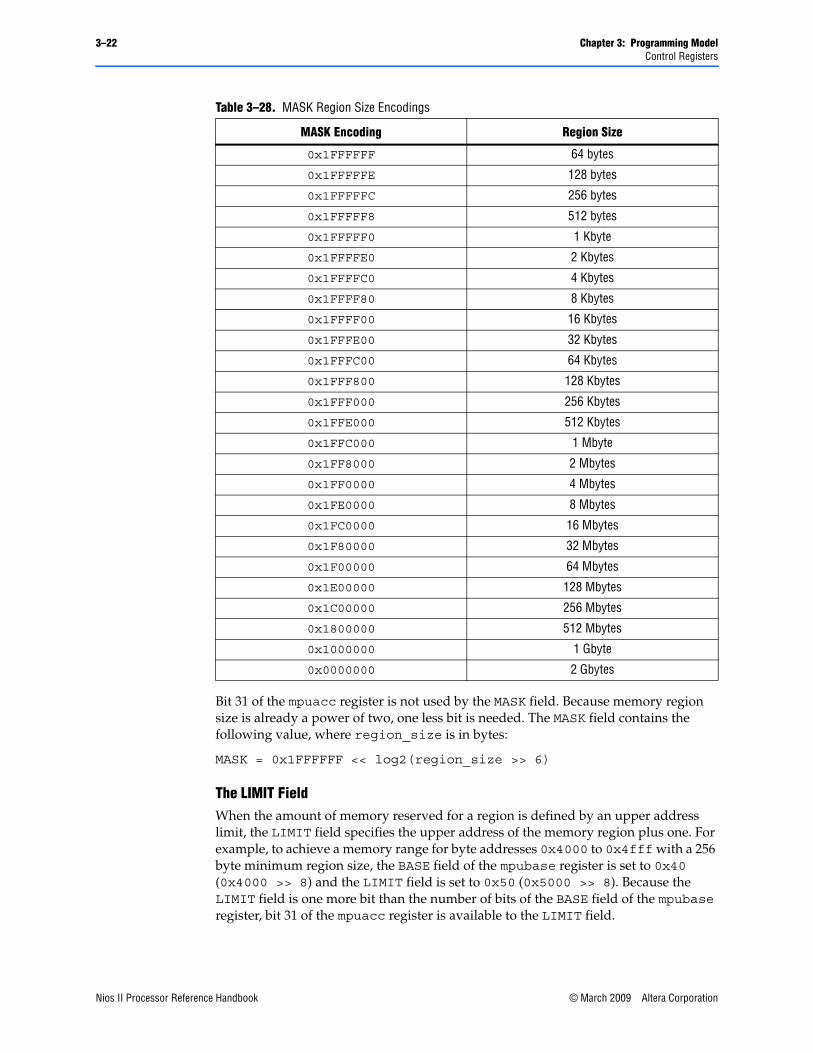
3–22 Chapter 3: Programming ModelControl Registers
Bit 31 of the mpuacc register is not used by the MASK field. Because memory region size is already a power of two, one less bit is needed. The MASK field contains the following value, where region_size is in bytes:
MASK = 0x1FFFFFF << log2(region_size >> 6)
The LIMIT FieldWhen the amount of memory reserved for a region is defined by an upper address limit, the LIMIT field specifies the upper address of the memory region plus one. For example, to achieve a memory range for byte addresses 0x4000 to 0x4fff with a 256 byte minimum region size, the BASE field of the mpubase register is set to 0x40 (0x4000 >> 8) and the LIMIT field is set to 0x50 (0x5000 >> 8). Because the LIMIT field is one more bit than the number of bits of the BASE field of the mpubase register, bit 31 of the mpuacc register is available to the LIMIT field.
Table 3–28. MASK Region Size Encodings
MASK Encoding Region Size
0x1FFFFFF 64 bytes
0x1FFFFFE 128 bytes
0x1FFFFFC 256 bytes
0x1FFFFF8 512 bytes
0x1FFFFF0 1 Kbyte
0x1FFFFE0 2 Kbytes
0x1FFFFC0 4 Kbytes
0x1FFFF80 8 Kbytes
0x1FFFF00 16 Kbytes
0x1FFFE00 32 Kbytes
0x1FFFC00 64 Kbytes
0x1FFF800 128 Kbytes
0x1FFF000 256 Kbytes
0x1FFE000 512 Kbytes
0x1FFC000 1 Mbyte
0x1FF8000 2 Mbytes
0x1FF0000 4 Mbytes
0x1FE0000 8 Mbytes
0x1FC0000 16 Mbytes
0x1F80000 32 Mbytes
0x1F00000 64 Mbytes
0x1E00000 128 Mbytes
0x1C00000 256 Mbytes
0x1800000 512 Mbytes
0x1000000 1 Gbyte
0x0000000 2 Gbytes
Nios II Processor Reference Handbook © March 2009 Altera CorporationPreliminary
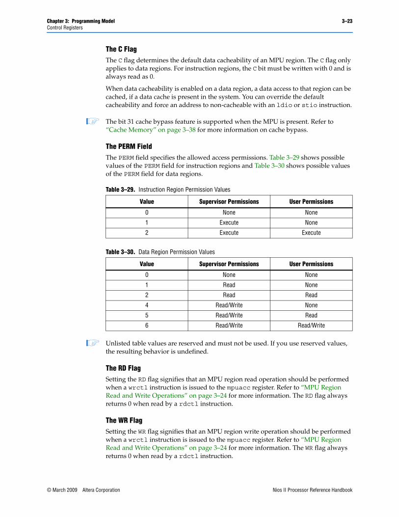
Chapter 3: Programming Model 3–23Control Registers
The C FlagThe C flag determines the default data cacheability of an MPU region. The C flag only applies to data regions. For instruction regions, the C bit must be written with 0 and is always read as 0.
When data cacheability is enabled on a data region, a data access to that region can be cached, if a data cache is present in the system. You can override the default cacheability and force an address to non-cacheable with an ldio or stio instruction.
1 The bit 31 cache bypass feature is supported when the MPU is present. Refer to “Cache Memory” on page 3–38 for more information on cache bypass.
The PERM FieldThe PERM field specifies the allowed access permissions. Table 3–29 shows possible values of the PERM field for instruction regions and Table 3–30 shows possible values of the PERM field for data regions.
1 Unlisted table values are reserved and must not be used. If you use reserved values, the resulting behavior is undefined.
The RD FlagSetting the RD flag signifies that an MPU region read operation should be performed when a wrctl instruction is issued to the mpuacc register. Refer to “MPU Region Read and Write Operations” on page 3–24 for more information. The RD flag always returns 0 when read by a rdctl instruction.
The WR FlagSetting the WR flag signifies that an MPU region write operation should be performed when a wrctl instruction is issued to the mpuacc register. Refer to “MPU Region Read and Write Operations” on page 3–24 for more information. The WR flag always returns 0 when read by a rdctl instruction.
Table 3–29. Instruction Region Permission Values
Value Supervisor Permissions User Permissions
0 None None
1 Execute None
2 Execute Execute
Table 3–30. Data Region Permission Values
Value Supervisor Permissions User Permissions
0 None None
1 Read None
2 Read Read
4 Read/Write None
5 Read/Write Read
6 Read/Write Read/Write
© March 2009 Altera Corporation Nios II Processor Reference HandbookPreliminary
3–24 Chapter 3: Programming ModelWorking with the MPU
1 Setting both the RD and WR flags to one results in undefined behavior.
Working with the MPUThis section provides a basic overview of MPU initialization and the MPU region read and write operations.
MPU Region Read and Write OperationsMPU region read and write operations are operations that access MPU region attributes through the mpubase and mpuacc control registers. The mpubase.BASE, mpuacc.MASK, mpuacc.LIMIT, mpuacc.C, and mpuacc.PERM fields comprise the MPU region attributes.
MPU region read operations retrieve the current values for the attributes of a region. Each MPU region read operation consists of the following actions:
■ Execute a wrctl instruction to the mpubase register with the mpubase.INDEX and mpubase.D fields set to identify the MPU region.
■ Execute a wrctl instruction to the mpuacc register with the mpuacc.RD field set to one and the mpuacc.WR field cleared to zero. This action loads the mpubase and mpuacc register values.
■ Execute a rdctl instruction to the mpubase register to read the loaded the mpubase register value.
■ Execute a rdctl instruction to the mpuacc register to read the loaded the mpuacc register value.
The MPU region read operation retrieves mpubase.BASE, mpuacc.MASK or mpuacc.LIMIT, mpuacc.C, and mpuacc.PERM values for the MPU region.
1 Values for the mpubase register are not actually retrieved until the wrctl instruction to the mpuacc register is performed.
MPU region write operations set new values for the attributes of a region. Each MPU region write operation consists of the following actions:
■ Execute a wrctl instruction to the mpubase register with the mpubase.INDEX and mpubase.D fields set to identify the MPU region.
■ Execute a wrctl instruction to the mpuacc register with the mpuacc.WR field set to one and the mpuacc.RD field cleared to zero.
The MPU region write operation sets the values for mpubase.BASE, mpuacc.MASK or mpuacc.LIMIT, mpuacc.C, and mpuacc.PERM as the new attributes for the MPU region.
Nios II Processor Reference Handbook © March 2009 Altera CorporationPreliminary
Chapter 3: Programming Model 3–25Exception Processing
Normally, a wrctl instruction flushes the pipeline to guarantee that any side effects of writing control registers take effect immediately after the wrctl instruction completes execution. However, wrctl instructions to the mpubase and mpuacc control registers do not automatically flush the pipeline. Instead, system software is responsible for flushing the pipeline as needed (either by using a flushp instruction or a wrctl instruction to a register that does flush the pipeline). Because a context switch typically requires reprogramming the MPU regions for the new thread, flushing the pipeline on each wrctl instruction would create unnecessary overhead.
MPU InitializationYour system software must provide a data structure that contains the region information described in “Memory Regions” on page 3–8 for each active thread. The data structure ideally contains two 32-bit values that correspond to the mpubase and mpuacc register formats.
The MPU is disabled on system reset. Before enabling the MPU, Altera recommends initializing all MPU regions. Enable desired instruction and data regions by writing each region’s attributes to the mpubase and mpuacc registers as described in “MPU Region Read and Write Operations” on page 3–24. You must also disable unused regions. When using region size, clear mpuacc.MASK to zero. When using limit, set the mpubase.BASE to a non-zero value and clear mpuacc.LIMIT to zero.
1 You must enable at least one instruction and one data region, otherwise unpredictable behavior might occur.
To perform a context switch, use a wrctl to write a zero to the PE field of the config register to disable the MPU, define all MPU regions from the new thread’s data structure, and then use another wrctl to write a one to config.PE to enable the MPU.
Define each region using the pair of wrctl instructions described in “MPU Region Read and Write Operations” on page 3–24. Repeat this dual wrctl instruction sequence until all desired regions are defined.
Debugger AccessThe debugger can access all MPU-related control registers using the normal wrctl and rdctl instructions. During debugging, the Nios II ignores the MPU, effectively temporarily disabling it.
Exception ProcessingAn exception is a transfer of control away from a program’s normal flow of execution, caused by an event, either internal or external to the processor, which requires immediate attention. Exception processing is the act of responding to an exception, and then returning to the pre-exception execution state.
Each of the Nios II exceptions falls into one of the following categories:
■ Reset exceptions
■ Break exceptions
© March 2009 Altera Corporation Nios II Processor Reference HandbookPreliminary
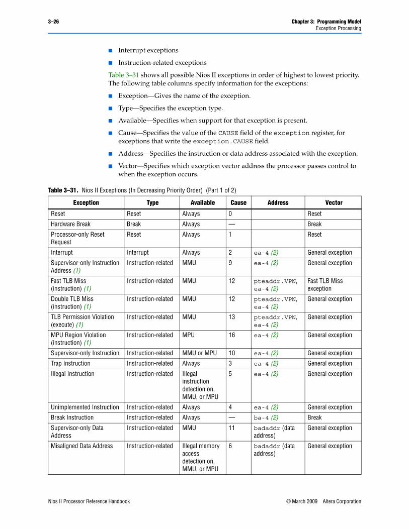
3–26 Chapter 3: Programming ModelException Processing
■ Interrupt exceptions
■ Instruction-related exceptions
Table 3–31 shows all possible Nios II exceptions in order of highest to lowest priority. The following table columns specify information for the exceptions:
■ Exception—Gives the name of the exception.
■ Type—Specifies the exception type.
■ Available—Specifies when support for that exception is present.
■ Cause—Specifies the value of the CAUSE field of the exception register, for exceptions that write the exception.CAUSE field.
■ Address—Specifies the instruction or data address associated with the exception.
■ Vector—Specifies which exception vector address the processor passes control to when the exception occurs.
Table 3–31. Nios II Exceptions (In Decreasing Priority Order) (Part 1 of 2)
Exception Type Available Cause Address Vector
Reset Reset Always 0 Reset
Hardware Break Break Always — Break
Processor-only Reset Request
Reset Always 1 Reset
Interrupt Interrupt Always 2 ea-4 (2) General exception
Supervisor-only Instruction Address (1)
Instruction-related MMU 9 ea-4 (2) General exception
Fast TLB Miss (instruction) (1)
Instruction-related MMU 12 pteaddr.VPN, ea-4 (2)
Fast TLB Miss exception
Double TLB Miss (instruction) (1)
Instruction-related MMU 12 pteaddr.VPN, ea-4 (2)
General exception
TLB Permission Violation (execute) (1)
Instruction-related MMU 13 pteaddr.VPN, ea-4 (2)
General exception
MPU Region Violation (instruction) (1)
Instruction-related MPU 16 ea-4 (2) General exception
Supervisor-only Instruction Instruction-related MMU or MPU 10 ea-4 (2) General exception
Trap Instruction Instruction-related Always 3 ea-4 (2) General exception
Illegal Instruction Instruction-related Illegal instruction detection on, MMU, or MPU
5 ea-4 (2) General exception
Unimplemented Instruction Instruction-related Always 4 ea-4 (2) General exception
Break Instruction Instruction-related Always — ba-4 (2) Break
Supervisor-only Data Address
Instruction-related MMU 11 badaddr (data address)
General exception
Misaligned Data Address Instruction-related Illegal memory access detection on, MMU, or MPU
6 badaddr (data address)
General exception
Nios II Processor Reference Handbook © March 2009 Altera CorporationPreliminary

Chapter 3: Programming Model 3–27Exception Processing
The following sections describe each exception type in detail.
Reset ExceptionsWhen a processor reset signal is asserted, the Nios II processor performs the following steps:
1. Clears the status register to 0x0.
2. Invalidates the instruction-cache line associated with the reset vector.
3. Begins executing the reset handler, located at the reset vector.
Clearing the status register disables hardware interrupts. If the MMU or MPU is present, clearing the status register forces the processor into supervisor mode.
Invalidating the reset cache line guarantees that instruction fetches for reset code comes from uncached memory.
Aside from the instruction-cache line associated with the reset vector, the contents of the cache memories are indeterminate after reset. To ensure cache coherency after reset, the reset handler located at the reset vector must immediately initialize the instruction cache. Next, either the reset handler or a subsequent routine should proceed to initialize the data cache.
The reset state is undefined for all other system components, including but not limited to:
■ General-purpose registers, except for zero (r0) which is permanently zero.
Misaligned Destination Address
Instruction-related Illegal memory access detection on, MMU, or MPU
7 badaddr (destination address)
General exception
Division Error Instruction-related Division error detection on
8 ea-4 (2) General exception
Fast TLB Miss (data) Instruction-related MMU 12 pteaddr.VPN, badaddr (data address)
Fast TLB Miss exception
Double TLB Miss (data) Instruction-related MMU 12 pteaddr.VPN, badaddr (data address)
General exception
TLB Permission Violation (read)
Instruction-related MMU 14 pteaddr.VPN, badaddr (data address)
General exception
TLB Permission Violation (write)
Instruction-related MMU 15 pteaddr.VPN, badaddr (data address)
General exception
MPU Region Violation (data)
Instruction-related MPU 17 badaddr (data address)
General exception
Notes to Table 3–31:
(1) It is possible for any instruction fetch to cause this exception.(2) Refer to Table 3–6 on page 3–11 for descriptions of the ea and ba registers.
Table 3–31. Nios II Exceptions (In Decreasing Priority Order) (Part 2 of 2)
Exception Type Available Cause Address Vector
© March 2009 Altera Corporation Nios II Processor Reference HandbookPreliminary
3–28 Chapter 3: Programming ModelException Processing
■ Control registers, except for status which is reset to 0x0.
■ Instruction and data memory.
■ Cache memory, except for the instruction-cache line associated with the reset vector.
■ Peripherals. Refer to the appropriate peripheral data sheet or specification for reset conditions.
■ Custom instruction logic. Refer to the Nios II Custom Instruction User Guide for reset conditions.
■ Nios II C-to-hardware (C2H) acceleration compiler logic.
Break ExceptionsA break is a transfer of control away from a program’s normal flow of execution for the purpose of debugging. Software debugging tools can take control of the Nios II processor via the JTAG debug module.
Break processing is the means by which software debugging tools implement debug and diagnostic features, such as breakpoints and watchpoints. Break processing is a type of exception processing, but the break mechanism is independent from general exception processing. A break can occur during exception processing, enabling debug tools to debug exception handlers.
The processor enters the break processing state under either of the following conditions:
■ The processor executes the break instruction. This is often referred to as a software break.
■ The JTAG debug module asserts a hardware break.
Processing a BreakA break causes the processor to take the following steps:
1. Stores the contents of the status register to bstatus.
2. Clears status.PIE to zero, disabling external processor interrupts.
3. Writes the address of the instruction following the break to the ba register (r30).
4. Clears status.U to zero, forcing the processor into supervisor mode, when the system contains an MMU or MPU.
5. Sets status.EH to one, indicating the processor is handling an exception, when the system contains an MMU.
6. Transfers execution to the break handler, stored at the break vector specified at system generation time.
Register UsageThe bstatus control register and general-purpose registers bt (r25) and ba (r30) are reserved for debugging. Code is not prevented from writing to these registers, but debug code might overwrite the values. The break handler can use bt (r25) to help save additional registers.
Nios II Processor Reference Handbook © March 2009 Altera CorporationPreliminary
Chapter 3: Programming Model 3–29Exception Processing
Returning From a BreakAfter processing a break, the break handler releases control of the processor by executing a bret instruction. The bret instruction restores status by copying the contents of bstatus and returns program execution to the address in the ba register (r30). Aside from bt, all registers are guaranteed to be returned to their pre-break state after returning from the break handler.
Interrupt ExceptionsAn external source such as a peripheral device can request a hardware interrupt by asserting one of the processor’s 32 interrupt-request inputs, irq0 through irq31. A hardware interrupt is generated if and only if all three of these conditions are true:
■ The PIE bit of the status control register is one.
■ An interrupt-request input, irqn, is asserted.
■ The corresponding bit n of the ienable control register is one.
Upon hardware interrupt, the processor clears the PIE bit to zero, disabling further interrupts, and performs the other steps outlined in “Processing Interrupt and Instruction-Related Exceptions” on page 3–35.
The value of the ipending control register shows which interrupt requests (IRQ) are pending. By peripheral design, an IRQ bit is guaranteed to remain asserted until the processor explicitly responds to the peripheral. Figure 3–2 shows the relationship between ipending, ienable, PIE, and the generation of an interrupt.
© March 2009 Altera Corporation Nios II Processor Reference HandbookPreliminary
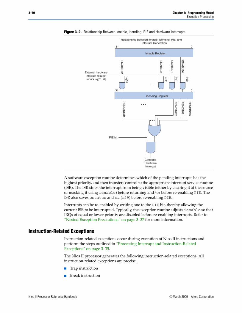
3–30 Chapter 3: Programming ModelException Processing
A software exception routine determines which of the pending interrupts has the highest priority, and then transfers control to the appropriate interrupt service routine (ISR). The ISR stops the interrupt from being visible (either by clearing it at the source or masking it using ienable) before returning and/or before re-enabling PIE. The ISR also saves estatus and ea (r29) before re-enabling PIE.
Interrupts can be re-enabled by writing one to the PIE bit, thereby allowing the current ISR to be interrupted. Typically, the exception routine adjusts ienable so that IRQs of equal or lower priority are disabled before re-enabling interrupts. Refer to “Nested Exception Precautions” on page 3–37 for more information.
Instruction-Related ExceptionsInstruction-related exceptions occur during execution of Nios II instructions and perform the steps outlined in “Processing Interrupt and Instruction-Related Exceptions” on page 3–35.
The Nios II processor generates the following instruction-related exceptions. All instruction-related exceptions are precise.
■ Trap instruction
■ Break instruction
Figure 3–2. Relationship Between ienable, ipending, PIE and Hardware Interrupts
IPE
ND
ING
0
IPE
ND
ING
1
IPE
ND
ING
2
ipending Register
IPE
ND
ING
31
irq0
irq1
irq2
irq31
31 0
IEN
AB
LE0
IEN
AB
LE1
IEN
AB
LE2
31 0
ienable Register
External hardwareinterrupt requestinputs irq[31..0]
Relationship Between ienable, ipending, PIE, and Interrupt Generation
. . .
. . .
. . .
PIE bit
GenerateHardware Interrupt
IEN
AB
LE31
Nios II Processor Reference Handbook © March 2009 Altera CorporationPreliminary
Chapter 3: Programming Model 3–31Exception Processing
■ Unimplemented instruction
■ Illegal instruction
■ Supervisor-only instruction
■ Supervisor-only instruction address
■ Supervisor-only data address
■ Misaligned data address
■ Misaligned destination address
■ Division error
■ Fast TLB miss
■ Double TLB miss
■ TLB permission violation
■ MPU region violation
Trap InstructionWhen a program issues the trap instruction, it generates a software trap exception. A program typically issues a software trap when the program requires servicing by the operating system. The general exception handler for the operating system determines the reason for the trap and responds appropriately.
Break InstructionThe break instruction is treated as a break exception. Refer to “Break Exceptions” on page 3–28 for details.
Unimplemented InstructionWhen the processor issues a valid instruction that is not implemented in hardware, an unimplemented instruction exception is generated. The general exception handler determines which instruction generated the exception. If the instruction is not implemented in hardware, control is passed to an exception routine that might choose to emulate the instruction in software. Refer to “Potential Unimplemented Instructions” on page 3–44 for more information.
Illegal InstructionIllegal instructions are instructions with an undefined opcode or opcode-extension field. The Nios II processor can check for illegal instructions and generate an exception when an illegal instruction is encountered. When your system contains an MMU or MPU, illegal instruction checking is always on. When no MMU or MPU is present, you have the option to have the processor check for illegal instructions.
f To see how to control this option, refer to the Instantiating the Nios II Processor in SOPC Builder chapter of the Nios II Processor Reference Handbook.
When the processor issues an instruction with an undefined opcode or opcode-extension field, and illegal instruction exception checking is turned on, an illegal instruction exception is generated.
© March 2009 Altera Corporation Nios II Processor Reference HandbookPreliminary
3–32 Chapter 3: Programming ModelException Processing
f Refer to the OP Encodings and OPX Encodings for R-Type Instructions tables in the Instruction Set Reference chapter of the Nios II Processor Reference Handbook to see the unused opcodes and opcode extensions.
1 All undefined opcodes are reserved. The processor does occasionally use some undefined encodings internally. Executing one of these undefined opcodes does not trigger an illegal instruction exception. Refer to the Nios II Core Implementation Details chapter of the Nios II Processor Reference Handbook for details on each specific Nios II core.
Supervisor-only InstructionWhen your system contains an MMU or MPU and the processor is in user mode (status.U = 1), executing a supervisor-only instruction results in a supervisor-only instruction exception. The supervisor-only instructions are initd, initi, eret, bret, rdctl, and wrctl.
This exception is implemented only in Nios II processors configured to use supervisor mode and user mode. Refer to “Operating Modes” on page 3–2 for more information.
Supervisor-only Instruction AddressWhen your system contains an MMU and the processor is in user mode (status.U = 1), attempts to access a supervisor-only instruction address result in a supervisor-only instruction address exception. Any instruction fetch can cause this exception. For definitions of supervisor-only address ranges, refer to Table 3–2 on page 3–5.
This exception is implemented only in Nios II processors that include the MMU.
Supervisor-only Data AddressWhen your system contains an MMU and the processor is in user mode (status.U = 1), any attempt to access a supervisor-only data address results in a supervisor-only data address exception. Instructions that can cause a supervisor-only data address exception are all loads, all stores, and flushda.
This exception is implemented only in Nios II processors that include the MMU.
Misaligned Data AddressThe Nios II processor can check for misaligned data addresses of load and store instructions and generate an exception when a misaligned data address is encountered. When your system contains an MMU or MPU, misaligned data address checking is always on. When no MMU or MPU is present, you have the option to have the processor check for misaligned data addresses.
f To see how to control this option, refer to the Instantiating the Nios II Processor in SOPC Builder chapter of the Nios II Processor Reference Handbook.
A data address is considered misaligned if the byte address is not a multiple of the width of the load or store instruction data width (four bytes for word, two bytes for half-word). Byte load and store instructions are always aligned so never take a misaligned address exception.
Nios II Processor Reference Handbook © March 2009 Altera CorporationPreliminary
Chapter 3: Programming Model 3–33Exception Processing
Misaligned Destination AddressThe Nios II processor can check for misaligned destination addresses of the callr, jmp, ret, eret, bret, and all branch instructions and generate an exception when a misaligned destination address is encountered. When your system contains an MMU or MPU, misaligned destination address checking is always on. When no MMU or MPU is present, you have the option to have the processor check for misaligned destination addresses.
f To see how to control this option, refer to the Instantiating the Nios II Processor in SOPC Builder chapter of the Nios II Processor Reference Handbook.
A destination address is considered misaligned if the target byte address of the instruction is not a multiple of four.
Division ErrorThe Nios II processor can check for division errors and generate an exception when a division error is encountered.
f To see how to control this option, refer to the Instantiating the Nios II Processor in SOPC Builder chapter of the Nios II Processor Reference Handbook.
The division error exception detects divide instructions that produce a quotient that can't be represented. The two cases are divide by zero and a signed division that divides the largest negative number -2147483648 (0x80000000) by -1 (0xffffffff). Division error detection is only available if divide instructions are supported by hardware.
Fast TLB MissFast TLB miss exceptions are implemented only in Nios II processors that include the MMU. The MMU has a special exception vector (fast TLB miss), specified in SOPC Builder at system generation time, specifically to handle TLB miss exceptions quickly. Whenever the processor cannot find a TLB entry matching the VPN (optionally extended by a process identifier), the result is a TLB miss exception. At the time of the exception, the processor first checks status.EH. When status.EH = 0, no other exception is already in process, so the processor considers the TLB miss a fast TLB miss, sets status.EH to one, and transfers control to the fast TLB miss exception handler (rather than to the general exception handler).
There are two kinds of fast TLB miss exceptions:
■ Fast TLB miss (instruction)—Any instruction fetch can cause this exception.
■ Fast TLB miss (data)—Load, store, initda, and flushda instructions can cause this exception.
The fast TLB miss exception handler can inspect the tlbmisc.D field to determine which kind of fast TLB miss exception occurred.
© March 2009 Altera Corporation Nios II Processor Reference HandbookPreliminary
3–34 Chapter 3: Programming ModelException Processing
Double TLB MissDouble TLB miss exceptions are implemented only in Nios II processors that include the MMU. When a TLB miss exception occurs while software is currently processing an exception (that is, when status.EH = 1), a double TLB miss exception is generated. Specifically, whenever the processor cannot find a TLB entry matching the VPN (optionally extended by a process identifier) and status.EH = 1, the result is a double TLB miss exception. The most common scenario is that a double TLB miss exception occurs during processing of a fast TLB miss exception. The processor preserves register values from the original exception and transfers control to the general exception handler which processes the newly-generated exception.
There are two kinds of double TLB miss exceptions:
■ Double TLB miss (instruction)—Any instruction fetch can cause this exception.
■ Double TLB miss (data)—Load, store, initda, and flushda instructions can cause this exception.
The general exception handler can inspect either the exception.CAUSE or tlbmisc.D field to determine which kind of double TLB miss exception occurred.
TLB Permission ViolationTLB permission violation exceptions are implemented only in Nios II processors that include the MMU. When a TLB entry is found matching the VPN (optionally extended by a process identifier), but the permissions do not allow the access to complete, a TLB permission violation exception is generated.
There are three kinds of TLB permission violation exceptions:
■ TLB permission violation (execute)—Any instruction fetch can cause this exception.
■ TLB permission violation (read)—Any load instruction can cause this exception.
■ TLB permission violation (write)—Any store instruction can cause this exception.
The general exception handler can inspect the exception.CAUSE field to determine which permissions were violated.
1 The data cache management instructions (initd, initda, flushd, and flushda) ignore the TLB permissions and do not generate TLB permission violation exceptions.
MPU Region ViolationMPU region violation exceptions are implemented only in Nios II processors that include the MPU. An MPU region violation exception is generated under any of the following conditions:
■ An instruction fetch or data address matched a region but the permissions for that region did not allow the action to complete.
■ An instruction fetch or data address did not match any region.
The general exception handler reads the MPU region attributes to determine if the address did not match any region or which permissions were violated.
There are two kinds of MPU region violation exceptions:
Nios II Processor Reference Handbook © March 2009 Altera CorporationPreliminary
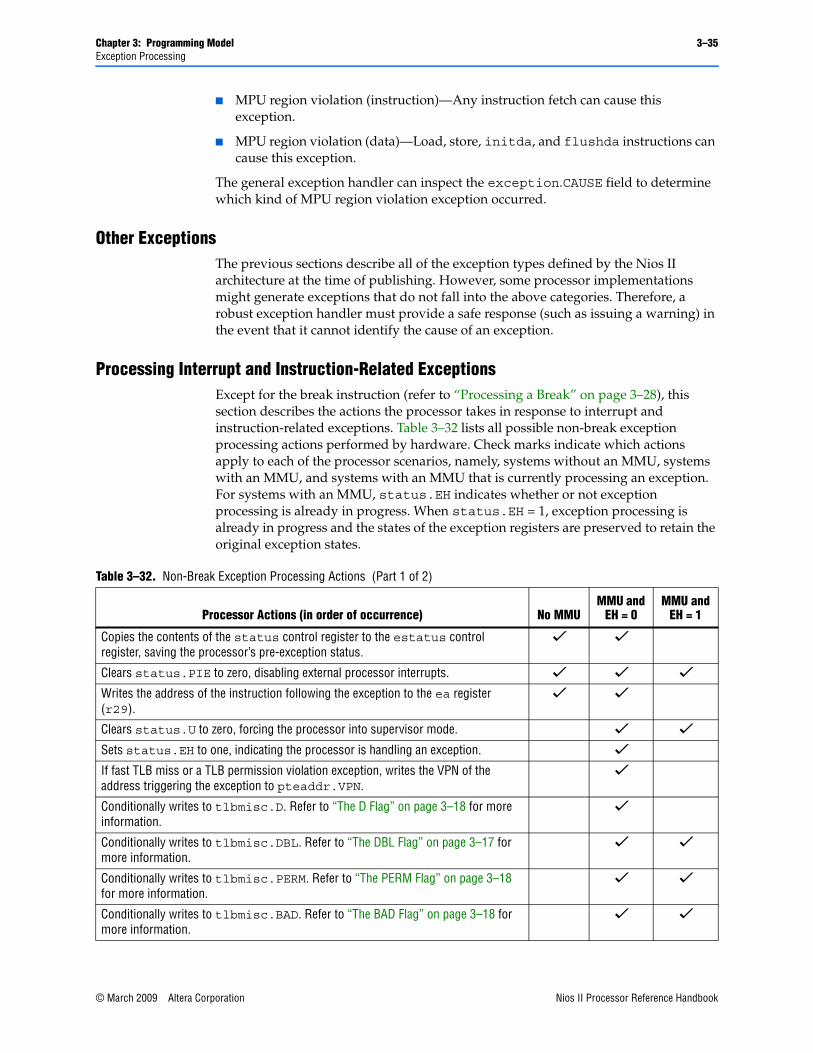
Chapter 3: Programming Model 3–35Exception Processing
■ MPU region violation (instruction)—Any instruction fetch can cause this exception.
■ MPU region violation (data)—Load, store, initda, and flushda instructions can cause this exception.
The general exception handler can inspect the exception.CAUSE field to determine which kind of MPU region violation exception occurred.
Other ExceptionsThe previous sections describe all of the exception types defined by the Nios II architecture at the time of publishing. However, some processor implementations might generate exceptions that do not fall into the above categories. Therefore, a robust exception handler must provide a safe response (such as issuing a warning) in the event that it cannot identify the cause of an exception.
Processing Interrupt and Instruction-Related ExceptionsExcept for the break instruction (refer to “Processing a Break” on page 3–28), this section describes the actions the processor takes in response to interrupt and instruction-related exceptions. Table 3–32 lists all possible non-break exception processing actions performed by hardware. Check marks indicate which actions apply to each of the processor scenarios, namely, systems without an MMU, systems with an MMU, and systems with an MMU that is currently processing an exception. For systems with an MMU, status.EH indicates whether or not exception processing is already in progress. When status.EH = 1, exception processing is already in progress and the states of the exception registers are preserved to retain the original exception states.
Table 3–32. Non-Break Exception Processing Actions (Part 1 of 2)
Processor Actions (in order of occurrence) No MMUMMU and
EH = 0MMU and
EH = 1
Copies the contents of the status control register to the estatus control register, saving the processor’s pre-exception status.
v v
Clears status.PIE to zero, disabling external processor interrupts. v v vWrites the address of the instruction following the exception to the ea register (r29).
v v
Clears status.U to zero, forcing the processor into supervisor mode. v vSets status.EH to one, indicating the processor is handling an exception. vIf fast TLB miss or a TLB permission violation exception, writes the VPN of the address triggering the exception to pteaddr.VPN.
v
Conditionally writes to tlbmisc.D. Refer to “The D Flag” on page 3–18 for more information.
v
Conditionally writes to tlbmisc.DBL. Refer to “The DBL Flag” on page 3–17 for more information.
v v
Conditionally writes to tlbmisc.PERM. Refer to “The PERM Flag” on page 3–18 for more information.
v v
Conditionally writes to tlbmisc.BAD. Refer to “The BAD Flag” on page 3–18 for more information.
v v
© March 2009 Altera Corporation Nios II Processor Reference HandbookPreliminary
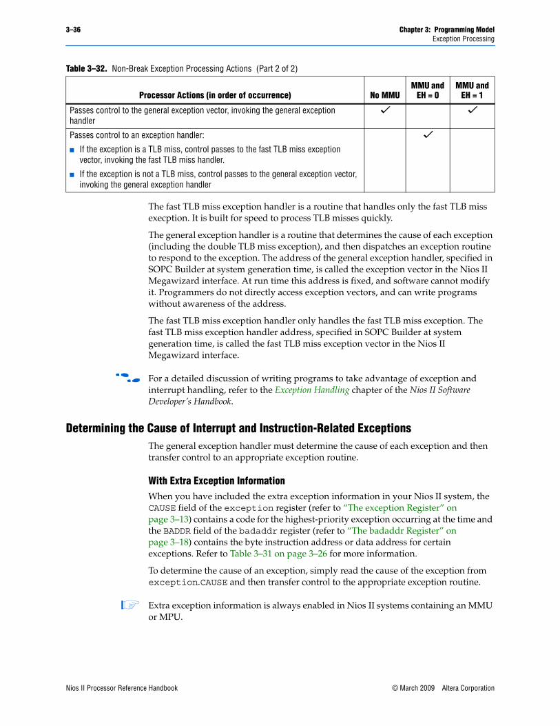
3–36 Chapter 3: Programming ModelException Processing
The fast TLB miss exception handler is a routine that handles only the fast TLB miss execption. It is built for speed to process TLB misses quickly.
The general exception handler is a routine that determines the cause of each exception (including the double TLB miss exception), and then dispatches an exception routine to respond to the exception. The address of the general exception handler, specified in SOPC Builder at system generation time, is called the exception vector in the Nios II Megawizard interface. At run time this address is fixed, and software cannot modify it. Programmers do not directly access exception vectors, and can write programs without awareness of the address.
The fast TLB miss exception handler only handles the fast TLB miss exception. The fast TLB miss exception handler address, specified in SOPC Builder at system generation time, is called the fast TLB miss exception vector in the Nios II Megawizard interface.
f For a detailed discussion of writing programs to take advantage of exception and interrupt handling, refer to the Exception Handling chapter of the Nios II Software Developer’s Handbook.
Determining the Cause of Interrupt and Instruction-Related ExceptionsThe general exception handler must determine the cause of each exception and then transfer control to an appropriate exception routine.
With Extra Exception InformationWhen you have included the extra exception information in your Nios II system, the CAUSE field of the exception register (refer to “The exception Register” on page 3–13) contains a code for the highest-priority exception occurring at the time and the BADDR field of the badaddr register (refer to “The badaddr Register” on page 3–18) contains the byte instruction address or data address for certain exceptions. Refer to Table 3–31 on page 3–26 for more information.
To determine the cause of an exception, simply read the cause of the exception from exception.CAUSE and then transfer control to the appropriate exception routine.
1 Extra exception information is always enabled in Nios II systems containing an MMU or MPU.
Passes control to the general exception vector, invoking the general exception handler
v v
Passes control to an exception handler:
■ If the exception is a TLB miss, control passes to the fast TLB miss exception vector, invoking the fast TLB miss handler.
■ If the exception is not a TLB miss, control passes to the general exception vector, invoking the general exception handler
v
Table 3–32. Non-Break Exception Processing Actions (Part 2 of 2)
Processor Actions (in order of occurrence) No MMUMMU and
EH = 0MMU and
EH = 1
Nios II Processor Reference Handbook © March 2009 Altera CorporationPreliminary
Chapter 3: Programming Model 3–37Exception Processing
Without Extra Exception InformationWhen you have not included the extra exception information in your Nios II system, your exception handler must determine the cause of exception itself. For this reason, Altera recommends always enabling the extra exception information.
When the extra exception information is not available, use the following sequence to determine the cause of an exception:
/* Check for interrupt exceptions first*/ if (estatus.EPIE == 1 and ipending != 0) {
handle interrupt /* Decode exception from instruction */ /* Note: Because the exception register is included with the MMU and */ /* MPU, you never need to determine MMU or MPU exceptions by decoding */ } else {
decode instruction at $ea-4 if (instruction is trap)
handle trap exception else if (instruction is load or store)
handle misaligned data address exception else if (instruction is branch, bret, callr, eret, jmp, or ret)
handle misaligned destination address exception else if (instruction is unimplemented)
handle unimplemented instruction exception else if (instruction is illegal)
handle illegal instruction exception else if (instruction is divide) {
if (denominator == 0) handle division error exception
else if (instruction is signed divide and numerator == 0x80000000 and denominator == 0xffffffff)
handle division error exception }
}
/* Not any known exception */ } else {
handle unknown exception (could be spurious interrupt) }
}
Nested Exception PrecautionsException routines must take special precautions before any of the following actions:
■ Issuing a trap instruction
■ Issuing a potentially unimplemented instruction
■ Re-enabling hardware interrupts
f For details about unimplemented instructions, refer to the Processor Architecture chapter of the Nios II Processor Reference Handbook.
Before allowing any of these actions, the exception routine must save estatus and ea (r29), then restore them properly before returning to preserve the pre-exception state of the exception registers.
© March 2009 Altera Corporation Nios II Processor Reference HandbookPreliminary
3–38 Chapter 3: Programming ModelMemory and Peripheral Access
Returning From Interrupt and Instruction-Related ExceptionsThe eret instruction is used to resume execution at the pre-exception address. Except for the et register (r24), the exception routine must restore any registers modified during exception processing before returning.
When executing the eret instruction, the processor performs the following tasks:
1. Copies the contents of estatus to status
2. Transfers program execution to the address in the ea register (r29)
Return Address ConsiderationsThe return address requires some consideration when returning from exception processing routines. After an exception occurs, ea contains the address of the instruction following the point where the exception occurred.
When returning from instruction-related exceptions, execution must resume from the instruction following the instruction where the exception occurred. Therefore, ea contains the correct return address.
On the other hand, hardware interrupt exceptions must resume execution from the interrupted instruction itself. In this case, the exception handler must subtract 4 from ea to point to the interrupted instruction.
Memory and Peripheral AccessNios II addresses are 32 bits, allowing access up to a 4 gigabyte address space. Nios II core implementations without MMUs restrict addresses to 31 bits or fewer. The MMU supports the full 32-bit physical address.
f For details, refer to the Nios II Core Implementation Details chapter of the Nios II Processor Reference Handbook.
Peripherals, data memory, and program memory are mapped into the same address space. The locations of memory and peripherals within the address space are determined at system generation time. Reading or writing to an address that does not map to a memory or peripheral produces an undefined result.
The processor’s data bus is 32 bits wide. Instructions are available to read and write byte, half-word (16-bit), or word (32-bit) data.
The Nios II architecture is little endian. For data wider than 8 bits stored in memory, the more-significant bits are located in higher addresses.
The Nios II architecture supports register+immediate addressing.
Cache MemoryThe Nios II architecture and instruction set accommodate the presence of data cache and instruction cache memories. Cache management is implemented in software by using cache management instructions. Instructions are provided to initialize the cache, flush the caches whenever necessary, and to bypass the data cache to properly access memory-mapped peripherals.
The Nios II architecture provides the following mechanisms to bypass the cache:
Nios II Processor Reference Handbook © March 2009 Altera CorporationPreliminary
Chapter 3: Programming Model 3–39Memory and Peripheral Access
■ When no MMU is present, bit 31 of the address is reserved for bit-31 cache bypass. With bit-31 cache bypass, the address space of processor cores is 2 GBytes, and the high bit of the address controls the caching of data memory accesses.
■ When the MMU is present, cacheability is controlled by the MMU, and bit 31 functions as a normal address bit. For details, refer to “Address Space and Memory Partitions” on page 3–4, and “TLB Organization” on page 3–6.
■ Cache bypass instructions, such as ldwio and stwio.
f Refer to the Nios II Core Implementation Details chapter of the Nios II Processor Reference Handbook for details of which processor cores implement bit-31 cache bypass. Refer to Instruction Set Reference chapter of the Nios II Processor Reference Handbook for details of the cache bypass instructions.
Code written for a processor core with cache memory behaves correctly on a processor core without cache memory. The reverse is not true. If it is necessary for a program to work properly on multiple Nios II processor core implementations, the program must behave as if the instruction and data caches exist. In systems without cache memory, the cache management instructions perform no operation, and their effects are benign.
f For a complete discussion of cache management, refer to the Cache and Tightly Coupled Memory chapter of the Nios II Software Developer’s Handbook.
Some consideration is necessary to ensure cache coherency after processor reset. Refer to “Reset Exceptions” on page 3–27 for more information.
f For details on the cache architecture and the memory hierarchy refer to the Processor Architecture chapter of the Nios II Processor Reference Handbook.
Virtual Address AliasingA virtual address alias occurs when two virtual addresses map to the same physical address. When an MMU and caches are present and the caches are larger than a page (4 KBytes), the operating system must prevent illegal virtual address aliases. Because the caches are virtually-indexed and physically-tagged, a portion of the virtual address is used to select the cache line. If the cache is 4 KBytes or less in size, the portion of the virtual address used to select the cache line fits with bits 11:0 of the virtual address which have the same value as bits 11:0 of the physical address (they are untranslated bits of the page offset). However, if the cache is larger than 4 KBytes, bits beyond the page offset (bits 12 and up) are used to select the cache line and these bits are allowed to be different than the corresponding physical address.
For example, in a 64 KByte direct-mapped cache with a 16-byte line, bits 15:4 are used to select the line. Assume that virtual address 0x1000 is mapped to physical address 0xF000 and virtual address 0x2000 is also mapped to physical address 0xF000. This is an illegal virtual address alias because accesses to virtual address 0x1000 use line 0x1 and accesses to virtual address 0x2000 use line 0x2 even though they map to the same physical address. This results in two copies of the same physical address in the cache. With an n-byte direct-mapped cache, there could be n/4096 copies of the same physical address in the cache if illegal virtual address aliases are not prevented. The bits of the virtual address that are used to select the line and are translated bits
© March 2009 Altera Corporation Nios II Processor Reference HandbookPreliminary
3–40 Chapter 3: Programming ModelInstruction Set Categories
(bits 12 and up) are known as the color of the address. An operating system avoids illegal virtual address aliases by ensuring that if multiple virtual addresses map the same physical address, the virtual addresses have the same color. Note though, the color of the virtual addresses does not need to be the same as the color as the physical address because the cache tag contains all the bits of the PFN.
Instruction Set CategoriesThis section introduces the Nios II instructions categorized by type of operation performed.
Data Transfer InstructionsThe Nios II architecture is a load-store architecture. Load and store instructions handle all data movement between registers, memory, and peripherals. Memories and peripherals share a common address space. Some Nios II processor cores use memory caching and/or write buffering to improve memory bandwidth. The architecture provides instructions for both cached and uncached accesses.
Table 3–33 describes the wide (32-bit) load and store instructions.
The data transfer instructions in Table 3–34 support byte and half-word transfers.
Table 3–33. Wide Data Transfer Instructions
Instruction Description
ldw
stw
The ldw and stw instructions load and store 32-bit data words from/to memory. The effective address is the sum of a register's contents and a signed immediate value contained in the instruction. Memory transfers can be cached or buffered to improve program performance. This caching and buffering might cause memory cycles to occur out of order, and caching might suppress some cycles entirely.
Data transfers for I/O peripherals should use ldwio and stwio.
ldwio
stwio
ldwio and stwio instructions load and store 32-bit data words from/to peripherals without caching and buffering. Access cycles for ldwio and stwio instructions are guaranteed to occur in instruction order and are never suppressed.
Table 3–34. Narrow Data Transfer Instructions
Instruction Description
ldb ldbu stb ldh ldhu sth
ldb, ldbu, ldh and ldhu load a byte or half-word from memory to a register. ldb and ldh sign-extend the value to 32 bits, and ldbu and ldhu zero-extend the value to 32 bits.
stb and sth store byte and half-word values, respectively.
Memory accesses can be cached or buffered to improve performance. To transfer data to I/O peripherals, use the “io” versions of the instructions, described below.
ldbio ldbuio stbio ldhio ldhuio sthio
These operations load/store byte and half-word data from/to peripherals without caching or buffering.
Nios II Processor Reference Handbook © March 2009 Altera CorporationPreliminary
Chapter 3: Programming Model 3–41Instruction Set Categories
Arithmetic and Logical InstructionsLogical instructions support and, or, xor, and nor operations. Arithmetic instructions support addition, subtraction, multiplication, and division operations. Refer to Table 3–35.
Move InstructionsThese instructions provide move operations to copy the value of a register or an immediate value to another register. Refer to Table 3–36.
Comparison InstructionsThe Nios II architecture supports a number of comparison instructions. All of these compare two registers or a register and an immediate value, and write either one (if true) or zero to the result register. These instructions perform all the equality and relational operators of the C programming language. Refer to Table 3–37.
Table 3–35. Arithmetic and Logical Instructions
Instruction Description
and or xor nor
These are the standard 32-bit logical operations. These operations take two register values and combine them bit-wise to form a result for a third register.
andi ori xori
These operations are immediate versions of the and, or, and xor instructions. The 16-bit immediate value is zero-extended to 32 bits, and then combined with a register value to form the result.
andhi orhi xorhi
In these versions of and, or, and xor, the 16-bit immediate value is shifted logically left by 16 bits to form a 32-bit operand. Zeroes are shifted in from the right.
add sub mul div divu
These are the standard 32-bit arithmetic operations. These operations take two registers as input and store the result in a third register.
addi subi muli
These instructions are immediate versions of the add, sub, and mul instructions. The instruction word includes a 16-bit signed value.
mulxss mulxuu
These instructions provide access to the upper 32 bits of a 32x32 multiplication operation. Choose the appropriate instruction depending on whether the operands should be treated as signed or unsigned values. It is not necessary to precede these instructions with a mul.
mulxsu This instruction is used in computing a 128-bit result of a 64x64 signed multiplication.
Table 3–36. Move Instructions
Instruction Description
mov movhi movi movui movia
mov copies the value of one register to another register. movi moves a 16-bit signed immediate value to a register, and sign-extends the value to 32 bits. movui and movhi move an immediate 16-bit value into the lower or upper 16-bits of a register, inserting zeros in the remaining bit positions. Use movia to load a register with an address.
© March 2009 Altera Corporation Nios II Processor Reference HandbookPreliminary
3–42 Chapter 3: Programming ModelInstruction Set Categories
Shift and Rotate InstructionsThe following instructions provide shift and rotate operations. The number of bits to rotate or shift can be specified in a register or an immediate value. Refer to Table 3–38.
Program Control InstructionsThe Nios II architecture supports the unconditional jump and call instructions listed in Table 3–39. These instructions do not have delay slots.
Table 3–37. Comparison Instructions
Instruction Description
cmpeq ==
cmpne !=
cmpge signed >=
cmpgeu unsigned >=
cmpgt signed >
cmpgtu unsigned >
cmple unsigned <=
cmpleu unsigned <=
cmplt signed <
cmpltu unsigned <
cmpeqi cmpnei cmpgei cmpgeui cmpgti cmpgtui cmplei cmpleui cmplti cmpltui
These instructions are immediate versions of the comparison operations. They compare the value of a register and a 16-bit immediate value. Signed operations sign-extend the immediate value to 32-bits. Unsigned operations fill the upper bits with zero.
Table 3–38. Shift and Rotate Instructions
Instruction Description
rol ror roli
The rol and roli instructions provide left bit-rotation. roli uses an immediate value to specify the number of bits to rotate. The ror instructions provides right bit-rotation.
There is no immediate version of ror, because roli can be used to implement the equivalent operation.
sll slli sra srl srai srli
These shift instructions implement the << and >> operators of the C programming language. The sll, slli, srl, srli instructions provide left and right logical bit-shifting operations, inserting zeros. The sra and srai instructions provide arithmetic right bit-shifting, duplicating the sign bit in the most significant bit. slli, srli and srai use an immediate value to specify the number of bits to shift.
Nios II Processor Reference Handbook © March 2009 Altera CorporationPreliminary
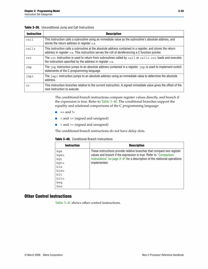
Chapter 3: Programming Model 3–43Instruction Set Categories
The conditional-branch instructions compare register values directly, and branch if the expression is true. Refer to Table 3–40. The conditional branches support the equality and relational comparisons of the C programming language:
■ == and !=
■ < and <= (signed and unsigned)
■ > and >= (signed and unsigned)
The conditional-branch instructions do not have delay slots.
Other Control InstructionsTable 3–41 shows other control instructions.
Table 3–39. Unconditional Jump and Call Instructions
Instruction Description
call This instruction calls a subroutine using an immediate value as the subroutine's absolute address, and stores the return address in register ra.
callr This instruction calls a subroutine at the absolute address contained in a register, and stores the return address in register ra. This instruction serves the roll of dereferencing a C function pointer.
ret The ret instruction is used to return from subroutines called by call or callr. ret loads and executes the instruction specified by the address in register ra.
jmp The jmp instruction jumps to an absolute address contained in a register. jmp is used to implement switch statements of the C programming language.
jmpi The jmpi instruction jumps to an absolute address using an immediate value to determine the absolute address.
or This instruction branches relative to the current instruction. A signed immediate value gives the offset of the next instruction to execute.
Table 3–40. Conditional-Branch Instructions
Instruction Description
bge bgeu bgt bgtu ble bleu blt bltu beq bne
These instructions provide relative branches that compare two register values and branch if the expression is true. Refer to “Comparison Instructions” on page 3–41 for a description of the relational operations implemented.
© March 2009 Altera Corporation Nios II Processor Reference HandbookPreliminary
3–44 Chapter 3: Programming ModelInstruction Set Categories
Custom InstructionsThe custom instruction provides low-level access to custom instruction logic. The inclusion of custom instructions is specified in SOPC Builder at system generation time, and the function implemented by custom instruction logic is design dependent.
f For further details, refer to the “Custom Instructions” section of the Processor Architecture chapter of the Nios II Processor Reference Handbook and the Nios II Custom Instruction User Guide.
Machine-generated C functions and assembly macros provide access to custom instructions, and hide implementation details from the user. Therefore, most software developers never use the custom assembly instruction directly.
No-Operation InstructionThe Nios II assembler provides a no-operation instruction, nop.
Potential Unimplemented InstructionsSome Nios II processor cores do not support all instructions in hardware. In this case, the processor generates an exception after issuing an unimplemented instruction. Only the following instructions can generate an unimplemented instruction exception:
■ mul
■ muli
■ mulxss
Table 3–41. Other Control Instructions
Instruction Description
trap eret
The trap and eret instructions generate and return from exceptions. These instructions are similar to the call/ret pair, but are used for exceptions. trap saves the status register in the estatus register, saves the return address in the ea register, and then transfers execution to the general exception handler. eret returns from exception processing by restoring status from estatus, and executing the instruction specified by the address in ea.
break bret
The break and bret instructions generate and return from breaks. break and bret are used exclusively by software debugging tools. Programmers never use these instructions in application code.
rdctl wrctl
These instructions read and write control registers, such as the status register. The value is read from or stored to a general-purpose register.
flushd flushda flushi initd initda initi
These instructions are used to manage the data and instruction cache memories.
flushp This instruction flushes all pre-fetched instructions from the pipeline. This is necessary before jumping to recently-modified instruction memory.
sync This instruction ensures that all previously-issued operations have completed before allowing execution of subsequent load and store operations.
Nios II Processor Reference Handbook © March 2009 Altera CorporationPreliminary
Chapter 3: Programming Model 3–45Referenced Documents
■ mulxsu
■ mulxuu
■ div
■ divu
■ initda
All other instructions are guaranteed not to generate an unimplemented instruction exception.
An exception routine must exercise caution if it uses these instructions, because they could generate another exception before the previous exception is properly handled. Refer to “Unimplemented Instruction” on page 3–31 for more information regarding unimplemented instruction processing.
Referenced DocumentsThis chapter references the following documents:
■ Nios II Software Developer’s Handbook
■ Processor Architecture chapter of the Nios II Processor Reference Handbook
■ Application Binary Interface chapter of the Nios II Processor Reference Handbook
■ Instruction Set Reference chapter of the Nios II Processor Reference Handbook
■ Instantiating the Nios II Processor in SOPC Builder chapter of the Nios II Processor Reference Handbook
■ Nios II Core Implementation Details chapter of the Nios II Processor Reference Handbook
■ Exception Handling chapter of the Nios II Software Developer’s Handbook
■ Cache and Tightly Coupled Memory chapter of the Nios II Software Developer’s Handbook
■ Processor Architecture chapter of the Nios II Processor Reference Handbook
■ Nios II Custom Instruction User Guide
Document Revision HistoryTable 3–42 shows the revision history for this document.
Table 3–42. Document Revision History (Part 1 of 2)
Date & Document Version Changes Made Summary of Changes
March 2009
v9.0.0
Maintenance release. —
November 2008
v8.1.0
Maintenance release. —
© March 2009 Altera Corporation Nios II Processor Reference HandbookPreliminary
3–46 Chapter 3: Programming ModelDocument Revision History
May 2008
v8.0.0
Added text to describe the MMU, MPU, and advanced exceptions. Added MMU, MPU, and advanced exceptions.
October 2007
v7.2.0
■ Reworked text to refer to break and reset as exceptions.
■ Grouped exceptions, break, reset, and interrupts all under Exception Processing.
■ Added table showing all Nios II exceptions (by priority).
■ Removed “ctl” references to control registers.
■ Added jmpi instruction to tables.
—
May 2007
v7.1.0
■ Added table of contents to Introduction section.
■ Added Referenced Documents section.
—
March 2007
v7.0.0
Maintenance release. —
November 2006
v6.1.0
Maintenance release. —
May 2006
v6.0.0
Maintenance release. —
October 2005
v5.1.0
Maintenance release. —
May 2005
v5.0.0
Maintenance release. —
September 2004
v1.1
■ Added details for new control register ctl5.
■ Updated details of debug and break processing to reflect new behavior of the break instruction.
—
May 2004
v1.0
Initial release. —
Table 3–42. Document Revision History (Part 2 of 2)
Date & Document Version Changes Made Summary of Changes
Nios II Processor Reference Handbook © March 2009 Altera CorporationPreliminary
© March 2009 Altera Corporation
NII51004-9.0.0
4. Instantiating the Nios II Processor in SOPC Builder
IntroductionThis chapter describes the Nios® II Processor MegaWizard interface in SOPC Builder. This chapter contains the following sections:
■ “Core Nios II Page” on page 4–1
■ “Caches and Memory Interfaces Page” on page 4–5
■ “Advanced Features Page” on page 4–8
■ “JTAG Debug Module Page” on page 4–13
■ “Custom Instructions Page” on page 4–16
The Nios II Processor MegaWizard interface allows you to specify the processor features for a particular Nios II hardware system. This chapter covers only the features of the Nios II processor that you can configure with the Nios II Processor MegaWizard interface. It is not a user guide for creating complete Nios II processor systems.
f To get started using SOPC Builder to design custom Nios II systems, refer to the Nios II Hardware Development Tutorial. Nios II development kits also provide a number of ready-made example hardware designs that demonstrate several different configurations of the Nios II processor.
The Nios II Processor MegaWizard interface has several pages. The following sections describe the settings available on each page.
1 Due to evolution and improvement of the Nios II Processor MegaWizard interface, the figures in this chapter might not match the exact screens that appear in SOPC Builder.
Core Nios II PageThe Core Nios II page presents the main settings for configuring the Nios II processor. Figure 4–1 shows an example of the Core Nios II page.
Nios II Processor Reference HandbookPreliminary
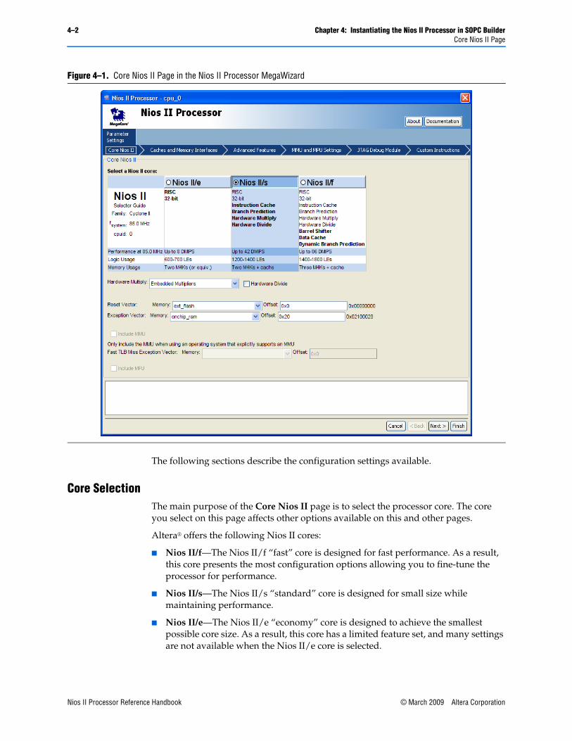
4–2 Chapter 4: Instantiating the Nios II Processor in SOPC BuilderCore Nios II Page
The following sections describe the configuration settings available.
Core SelectionThe main purpose of the Core Nios II page is to select the processor core. The core you select on this page affects other options available on this and other pages.
Altera® offers the following Nios II cores:
■ Nios II/f—The Nios II/f “fast” core is designed for fast performance. As a result, this core presents the most configuration options allowing you to fine-tune the processor for performance.
■ Nios II/s—The Nios II/s “standard” core is designed for small size while maintaining performance.
■ Nios II/e—The Nios II/e “economy” core is designed to achieve the smallest possible core size. As a result, this core has a limited feature set, and many settings are not available when the Nios II/e core is selected.
Figure 4–1. Core Nios II Page in the Nios II Processor MegaWizard
Nios II Processor Reference Handbook © March 2009 Altera CorporationPreliminary
Chapter 4: Instantiating the Nios II Processor in SOPC Builder 4–3Core Nios II Page
As shown in Figure 4–1, the Core Nios II page displays a “selector guide” table that lists the basic properties of each core.
f For complete details of each core, refer to the Nios II Core Implementation Details chapter of the Nios II Processor Reference Handbook.
Multiply and Divide SettingsThe Nios II/s and Nios II/f cores offer hardware multiply and divide options. You can choose the best option to balance embedded multiplier usage, logic element (LE) usage, and performance.
The Hardware Multiply setting for each core provides a subset of the options in the following list:
■ DSP Block—Include DSP block multipliers in the arithmetic logic unit (ALU). This option is only present when targeting devices that have DSP block multipliers.
■ Embedded Multipliers—Include embedded multipliers in the ALU. This option is only present when targeting FPGA devices that have embedded multipliers.
■ Logic Elements—Include LE-based multipliers in the ALU. This option achieves high multiply performance without consuming embedded multiplier resources.
■ None—This option conserves logic resources by eliminating multiply hardware. Multiply operations are implemented in software.
Turning on Hardware Divide includes LE-based divide hardware in the ALU. The Hardware Divide option achieves much greater performance than software emulation of divide operations.
f For details on the performance effects of the Hardware Multiply and Hardware Divide options, refer to the Nios II Core Implementation Details chapter of the Nios II Processor Reference Handbook.
Reset VectorYou can select the memory module where the reset code (boot loader) resides, and the location of the reset vector (reset address). The reset vector cannot be configured until your system memory components are in place.
The Memory list, which includes all memory modules mastered by the Nios II processor, allows you to select the reset vector memory module. In a typical system, you select a nonvolatile memory module for the reset code.
Offset allows you to specify the location of the reset vector relative to the memory module’s base address. SOPC Builder calculates the physical address of the reset vector when you modify the memory module, the offset, or the memory module’s base address, and displays the address next to the Offset box. This address, displayed next to the Offset box, is always a physical address, even when an MMU is present.
f For details on reset exceptions, refer to the Programming Model chapter of the Nios II Processor Reference Handbook.
© March 2009 Altera Corporation Nios II Processor Reference HandbookPreliminary
4–4 Chapter 4: Instantiating the Nios II Processor in SOPC BuilderCore Nios II Page
General Exception VectorYou can select the memory module where the general exception vector (exception address) resides, and the location of the general exception vector. The general exception vector cannot be configured until your system memory components are in place.
The Memory list, which includes all memory modules mastered by the Nios II processor, allows you to select the exception vector memory module. In a typical system, you select a low-latency memory module for the exception code.
Offset allows you to specify the location of the exception vector relative to the memory module’s base address. SOPC Builder calculates the physical address of the exception vector when you modify the memory module, the offset, or the memory module’s base address. This address, displayed next to the Offset box, is always a physical address, even when an MMU is present.
For details on exceptions, refer to the Programming Model chapter of the Nios II Processor Reference Handbook.
Memory Management Unit SettingsThe Nios II/f core offers a memory management unit (MMU) to support full-featured operating systems. Turning on Include MMU includes the Nios II MMU in your Nios II hardware system.
1 Do not include an MMU in your Nios II system unless your operating system requires it. The MMU is only useful with software that takes advantage of it. Many Nios II systems involve simpler system software, such as Altera® HAL or MicroC/OS-II. Such software is unlikely to function correctly with an MMU-based Nios II processor.
Fast TLB Miss Exception VectorThe fast TLB miss exception vector is a special exception vector used exclusively by the MMU to handle TLB miss exceptions. You can select the memory module where the fast TLB miss exception vector (exception address) resides, and the location of the fast TLB miss exception vector. The fast TLB miss exception vector cannot be configured until your system memory components are in place.
The Memory list, which includes all memory modules mastered by the Nios II processor, allows you to select the exception vector memory module. In a typical system, you select a low-latency memory module for the exception code.
Offset allows you to specify the location of the exception vector relative to the memory module’s base address. SOPC Builder calculates the physical address of the exception vector when you modify the memory module, the offset, or the memory module’s base address. This address, displayed next to the Offset box, is always a physical address.
1 The Nios II MMU is optional and mutually exclusive from the Nios II MPU. Nios II systems can include either an MMU or MPU, but cannot include both an MMU and MPU in the same design.
f For details on the Nios II MMU, refer to the Programming Model chapter of the Nios II Processor Reference Handbook.
Nios II Processor Reference Handbook © March 2009 Altera CorporationPreliminary
Chapter 4: Instantiating the Nios II Processor in SOPC Builder 4–5Caches and Memory Interfaces Page
1 To function correctly with the MMU, the base physical address of all exception vectors (reset, general exception, break, and fast TLB miss) must point to low physical memory so that hardware can correctly map their virtual addresses into the kernel partition. This restriction is enforced by the Nios II Processor MegaWizard interface.
Memory Protection Unit SettingsThe Nios II/f core offers a memory protection unit (MPU) to support operating systems and runtime environments that desire memory protection without the overhead of virtual memory management. Turning on Include MPU includes the Nios II MPU in your Nios II hardware system.
1 The Nios II MPU is optional and mutually exclusive from the Nios II MMU. Nios II systems can include either an MPU or MMU, but cannot include both an MPU and MMU in the same design.
f For details on the Nios II MPU, refer to the Programming Model chapter of the Nios II Processor Reference Handbook.
Caches and Memory Interfaces PageThe Caches and Memory Interfaces page allows you to configure the cache and tightly-coupled memory usage for the instruction and data master ports. Figure 4–2 shows an example of the Caches and Memory Interfaces page.
© March 2009 Altera Corporation Nios II Processor Reference HandbookPreliminary
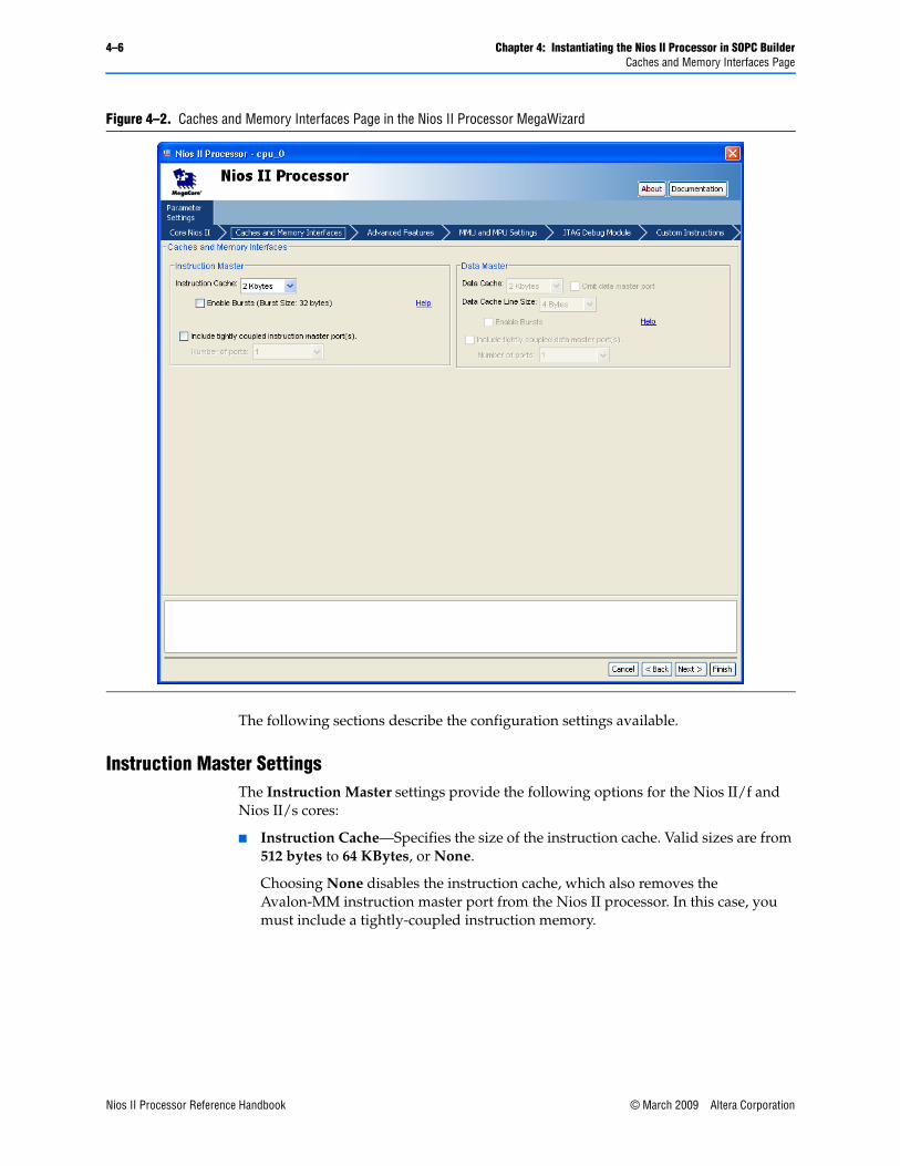
4–6 Chapter 4: Instantiating the Nios II Processor in SOPC BuilderCaches and Memory Interfaces Page
The following sections describe the configuration settings available.
Instruction Master SettingsThe Instruction Master settings provide the following options for the Nios II/f and Nios II/s cores:
■ Instruction Cache—Specifies the size of the instruction cache. Valid sizes are from 512 bytes to 64 KBytes, or None.
Choosing None disables the instruction cache, which also removes the Avalon-MM instruction master port from the Nios II processor. In this case, you must include a tightly-coupled instruction memory.
Figure 4–2. Caches and Memory Interfaces Page in the Nios II Processor MegaWizard
Nios II Processor Reference Handbook © March 2009 Altera CorporationPreliminary
Chapter 4: Instantiating the Nios II Processor in SOPC Builder 4–7Caches and Memory Interfaces Page
■ Enable Bursts—The Nios II processor can fill its instruction cache lines using burst transfers. Usually you enable bursts on the processor's instruction master when instructions are stored in DRAM, and disable bursts when instructions are stored in SRAM.
Bursting to DRAM typically improves memory bandwidth, but might consume additional FPGA resources. Be aware that when bursts are enabled, accesses to slaves might go through additional hardware (called "burst adapters") which might decrease fMAX.
When the Nios II processor transfers execution to the first word of a cache line, the processor fills the line by executing a sequence of word transfers that have ascending addresses, such as 0, 4, 8, 12, 16, 20, 24, 28.
However, when the Nios II processor transfers execution to an instruction that is not the first word of a cache line, the processor fetches the required (or "critical") instruction first, and then fills the rest of the cache line. The addresses of a burst increase until the last word of the cache line is filled, and then continue with the first word of the cache line. For example, with a 32-byte cache line, transferring control to address 8 results in a burst with the following address sequence: 8, 12, 16, 20, 24, 28, 0, 4.
■ Include tightly coupled instruction master port(s)—When on, the Nios II processor includes tightly-coupled memory ports. You can specify one to four ports with the Number of ports setting. Tightly-coupled memory ports appear on the connection panel of the Nios II processor in the SOPC Builder System Contents tab. You must connect each port to exactly one memory component in the system.
Data Master SettingsThe Data Master settings provide the following options for the Nios II/f core:
■ Data Cache—Specifies the size of the data cache. Valid sizes are from 512 bytes to 64 KBytes, or None. Depending on the value specified for Data Cache, the following options are available:
■ Data Cache Line Size—Valid sizes are 4 bytes, 16 bytes, or 32 bytes.
■ Omit data master port—If you set Data Cache to None, you can optionally turn on Omit data master port to remove the Avalon-MM data master port from the Nios II processor. In this case, you must include a tightly-coupled data memory.
© March 2009 Altera Corporation Nios II Processor Reference HandbookPreliminary
4–8 Chapter 4: Instantiating the Nios II Processor in SOPC BuilderAdvanced Features Page
1 Although the Nios II processor can operate entirely out of tightly-coupled memory without the need for Avalon-MM instruction or data masters, software debug is not possible when either the Avalon-MM instruction or data master is omitted.
Enable Bursts—The Nios II processor can fill its data cache lines using burst transfers. Usually you enable bursts on the processor's data bus when processor data is stored in DRAM, and disable bursts when processor data is stored in SRAM.
Bursting to DRAM typically improves memory bandwidth but might consume additional FPGA resources. Be aware that when bursts are enabled, accesses to slaves might go through additional hardware (called "burst adapters") which might decrease fMAX.
Bursting is only enabled for data line sizes greater than 4 bytes. The burst length is 4 for a 16 byte line size and 8 for a 32 byte line size. Data cache bursts are always aligned on the cache line boundary. For example, with a 32-byte Nios II data cache line, a cache miss to the address 8 results in a burst with the following address sequence: 0, 4, 8, 12, 16, 20, 24 and 28.
■ Include tightly coupled data master port(s)—When on, the Nios II processor includes tightly-coupled memory ports. You can specify one to four ports with the Number of ports setting. Tightly-coupled memory ports appear on the connection panel of the Nios II processor in the SOPC Builder System Contents tab. You must connect each port to exactly one memory component in the system.
Advanced Features PageThe Advanced Features page allows you to enable specialized features of the Nios II processor. Figure 4–3 shows the Advanced Features page.
Nios II Processor Reference Handbook © March 2009 Altera CorporationPreliminary
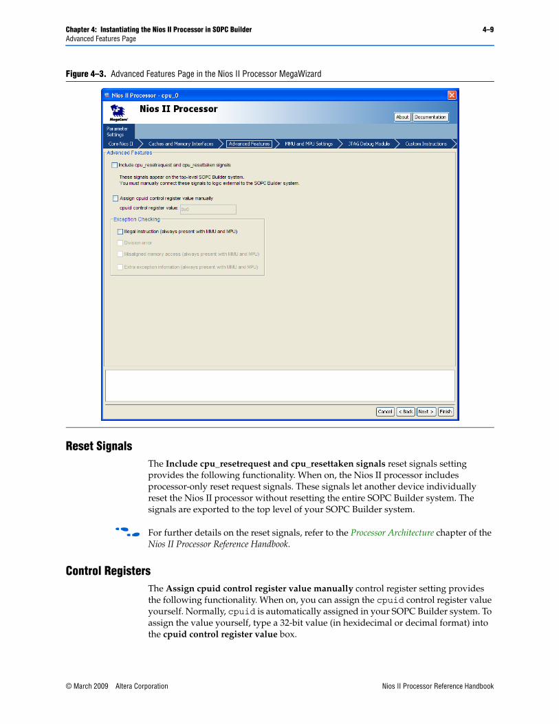
Chapter 4: Instantiating the Nios II Processor in SOPC Builder 4–9Advanced Features Page
Reset SignalsThe Include cpu_resetrequest and cpu_resettaken signals reset signals setting provides the following functionality. When on, the Nios II processor includes processor-only reset request signals. These signals let another device individually reset the Nios II processor without resetting the entire SOPC Builder system. The signals are exported to the top level of your SOPC Builder system.
f For further details on the reset signals, refer to the Processor Architecture chapter of the Nios II Processor Reference Handbook.
Control RegistersThe Assign cpuid control register value manually control register setting provides the following functionality. When on, you can assign the cpuid control register value yourself. Normally, cpuid is automatically assigned in your SOPC Builder system. To assign the value yourself, type a 32-bit value (in hexidecimal or decimal format) into the cpuid control register value box.
Figure 4–3. Advanced Features Page in the Nios II Processor MegaWizard
© March 2009 Altera Corporation Nios II Processor Reference HandbookPreliminary
4–10 Chapter 4: Instantiating the Nios II Processor in SOPC BuilderAdvanced Features Page
Exception CheckingThe Exception Checking settings provide the following options:
■ Illegal instruction—When Illegal instruction is on, the processor generates an illegal instruction exception when an instruction with an undefined opcode or opcode-extension field is executed.
1 When your system contains an MMU or MPU, the processor automatically generates illegal instruction exceptions. Therefore, the Illegal instruction setting is always disabled when the Core Nios II page Include MMU or Include MPU are on.
■ Division error—Division error detection is only available for the Nios II/f core, and only then when Hardware Divide on the Core Nios II page is on. When divide instructions are not supported by hardware, the Division error setting is disabled.
When Division error is on, the processor generates a division error exception when it detects divide instructions that produce a result that cannot be represented in the destination register. This only happens in the following two cases:
■ Divide by zero
■ Divide overflow—A signed division that divides the largest negative number -2147483648 (0x80000000) by -1 (0xffffffff).
■ Misaligned memory access—Misaligned memory access detection is only available for the Nios II/f core. When Misaligned memory access is on, the processor checks for misaligned memory accesses.
1 When your system contains an MMU or MPU, the processor automatically generates misaligned memory access exceptions. Therefore, the Misaligned memory access checkbox is always disabled when Include MMU or Include MPU on the Core Nios II page are on.
There are two misaligned memory address exceptions:
■ Misaligned data address—Data addresses of load and store instructions are checked for misalignment. A data address is considered misaligned if the byte address is not a multiple of the data width of the load or store instruction (4 bytes for word, 2 bytes for half-word). Byte load and store instructions are always aligned so never generate a misaligned data address exception.
■ Misaligned destination address—Destination instruction addresses of br, callr, jmp, ret, eret, and bret instructions are checked for misalignment. A destination instruction address is considered misaligned if the target byte address of the instruction is not a multiple of four.
■ Extra exception information—When Extra exception information is on, non-break exceptions store a code in the CAUSE field of the exception control register to indicate the cause of the exception.
Nios II Processor Reference Handbook © March 2009 Altera CorporationPreliminary
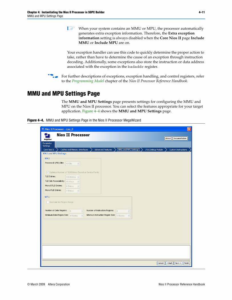
Chapter 4: Instantiating the Nios II Processor in SOPC Builder 4–11MMU and MPU Settings Page
1 When your system contains an MMU or MPU, the processor automatically generates extra exception information. Therefore, the Extra exception information setting is always disabled when the Core Nios II page Include MMU or Include MPU are on.
Your exception handler can use this code to quickly determine the proper action to take, rather than have to determine the cause of an exception through instruction decoding. Additionally, some exceptions also store the instruction or data address associated with the exception in the badaddr register.
f For further descriptions of exceptions, exception handling, and control registers, refer to the Programming Model chapter of the Nios II Processor Reference Handbook.
MMU and MPU Settings PageThe MMU and MPU Settings page presents settings for configuring the MMU and MPU on the Nios II processor. You can select the features appropriate for your target application. Figure 4–4 shows the MMU and MPU Settings page.
Figure 4–4. MMU and MPU Settings Page in the Nios II Processor MegaWizard
© March 2009 Altera Corporation Nios II Processor Reference HandbookPreliminary
4–12 Chapter 4: Instantiating the Nios II Processor in SOPC BuilderMMU and MPU Settings Page
MMUWhen Include MMU on the Core Nios II page is on, the MMU settings on the MMU and MPU Settings page provide the following options for the MMU in the Nios II/f core. Typically, you should not need to change any of these settings from their default values.
■ Process ID (PID) Bits—Specifies the number of bits to use to represent the process identifier.
■ Optimize number of TLB entries based on device family—When on, specifies the optimal number of TLB entries to allocate based on the device family of the target hardware and disables TLB Entries.
■ TLB Entries—Specifies the number of entries in the translation lookaside buffer (TLB).
■ TLB Set-Associativity—Specifies the number of set-associativity ways in the TLB.
■ Micro ITLB Entries—Specifies the number of entries in the micro instruction TLB.
■ Micro DTLB Entries—Specifies the number of entries in the micro data TLB.
f For details on the MMU, refer to the Programming Model chapter of the Nios II Processor Reference Handbook. For specifics on the Nios II/f core, refer to the Nios II Core Implementation Details chapter of the Nios II Processor Reference Handbook.
MPUWhen Include MPU on the Core Nios II page is on, the MPU settings on the MMU and MPU Settings page provide the following options for the MPU in the Nios II/f core.
■ Use Limit for Region Range—Controls whether the amount of memory in the region is defined by size or upper address limit is defined by size or upper address limit. When on, the amount of memory is based on the given upper address limit. When off, the amount of memory is based on the given size.
■ Number of Data Regions—Specifies the number of data regions to allocate. Allowed values range from 2 to 32.
■ Minimum Data Region Size—Specifies the minimum data region size. Allowed values range from 64 bytes to 1 Mbyte and must be a power of two.
■ Number of Instruction Regions—Specifies the number of instruction regions to allocate. Allowed values range from 2 to 32.
■ Minimum Instruction Region Size—Specifies the minimum instruction region size. Allowed values range from 64 bytes to 1 Mbyte and must be a power of two.
1 The maximum region size is the size of the Nios II instruction and data addresses automatically determined when the Nios II system is generated in SOPC Builder. Maximum region size is based on the address range of slaves connected to the Nios II instruction and data masters.
f For details on the MPU, refer to the Programming Model chapter of the Nios II Processor Reference Handbook. For specifics on the Nios II/f core, refer to the Nios II Core Implementation Details chapter of the Nios II Processor Reference Handbook.
Nios II Processor Reference Handbook © March 2009 Altera CorporationPreliminary
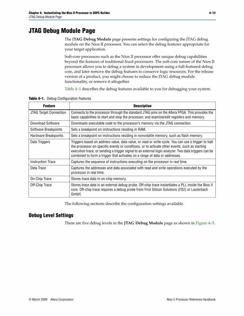
Chapter 4: Instantiating the Nios II Processor in SOPC Builder 4–13JTAG Debug Module Page
JTAG Debug Module PageThe JTAG Debug Module page presents settings for configuring the JTAG debug module on the Nios II processor. You can select the debug features appropriate for your target application.
Soft-core processors such as the Nios II processor offer unique debug capabilities beyond the features of traditional fixed processors. The soft-core nature of the Nios II processor allows you to debug a system in development using a full-featured debug core, and later remove the debug features to conserve logic resources. For the release version of a product, you might choose to reduce the JTAG debug module functionality, or remove it altogether.
Table 4–1 describes the debug features available to you for debugging your system.
The following sections describe the configuration settings available.
Debug Level SettingsThere are five debug levels in the JTAG Debug Module page as shown in Figure 4–5.
Table 4–1. Debug Configuration Features
Feature Description
JTAG Target Connection Connects to the processor through the standard JTAG pins on the Altera FPGA. This provides the basic capabilities to start and stop the processor, and examine/edit registers and memory.
Download Software Downloads executable code to the processor’s memory via the JTAG connection.
Software Breakpoints Sets a breakpoint on instructions residing in RAM.
Hardware Breakpoints Sets a breakpoint on instructions residing in nonvolatile memory, such as flash memory.
Data Triggers Triggers based on address value, data value, or read or write cycle. You can use a trigger to halt the processor on specific events or conditions, or to activate other events, such as starting execution trace, or sending a trigger signal to an external logic analyzer. Two data triggers can be combined to form a trigger that activates on a range of data or addresses.
Instruction Trace Captures the sequence of instructions executing on the processor in real time.
Data Trace Captures the addresses and data associated with read and write operations executed by the processor in real time.
On-Chip Trace Stores trace data in on-chip memory.
Off-Chip Trace Stores trace data in an external debug probe. Off-chip trace instantiates a PLL inside the Nios II core. Off-chip trace requires a debug probe from First Silicon Solutions (FS2) or Lauterbach GmbH.
© March 2009 Altera Corporation Nios II Processor Reference HandbookPreliminary
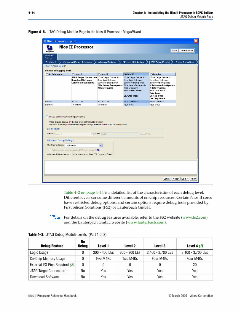
4–14 Chapter 4: Instantiating the Nios II Processor in SOPC BuilderJTAG Debug Module Page
Table 4–2 on page 4–14 is a detailed list of the characteristics of each debug level. Different levels consume different amounts of on-chip resources. Certain Nios II cores have restricted debug options, and certain options require debug tools provided by First Silicon Solutions (FS2) or Lauterbach GmbH.
f For details on the debug features available, refer to the FS2 website (www.fs2.com) and the Lauterbach GmbH website (www.lauterbach.com).
Figure 4–5. JTAG Debug Module Page in the Nios II Processor MegaWizard
Table 4–2. JTAG Debug Module Levels (Part 1 of 2)
Debug FeatureNo
Debug Level 1 Level 2 Level 3 Level 4 (1)
Logic Usage 0 300 - 400 LEs 800 - 900 LEs 2,400 - 2,700 LEs 3,100 - 3,700 LEs
On-Chip Memory Usage 0 Two M4Ks Two M4Ks Four M4Ks Four M4Ks
External I/O Pins Required (2) 0 0 0 0 20
JTAG Target Connection No Yes Yes Yes Yes
Download Software No Yes Yes Yes Yes
Nios II Processor Reference Handbook © March 2009 Altera CorporationPreliminary
Chapter 4: Instantiating the Nios II Processor in SOPC Builder 4–15JTAG Debug Module Page
Debug SignalsThe Include debugreq and debugack signals debug signals setting provides the following functionality. When on, the Nios II processor includes debug request and acknowledge signals. These signals let another device temporarily suspend the Nios II processor for debug purposes. The signals are exported to the top level of your SOPC Builder system.
f For further details on the debug signals, refer to the Processor Architecture chapter of the Nios II Processor Reference Handbook.
Break VectorIf the Nios II processor contains a JTAG debug module, SOPC Builder determines a break vector (break address). Memory is always the processor core you are configuring. Offset is fixed at 0x20. SOPC Builder calculates the physical address of the break vector from the memory module’s base address and the offset.
Advanced Debug SettingsDebug levels 3 and 4 support trace data collection into an on-chip memory buffer. You can set the on-chip trace buffer size to sizes from 128 to 64K trace frames, using OCI Onchip Trace. Larger buffer sizes consume more on-chip M4K RAM blocks. Every M4K RAM block can store up to 128 trace frames.
1 The Nios II MMU does not support the JTAG debug module trace.
Debug level 4 also supports manual 2X clock signal specification. If you want to use a specific 2X clock signal in your FPGA design, turn off Automatically generate internal 2X clock signal and drive a 2X clock signal into your SOPC Builder system manually.
f For further details on trace frames, refer to the Processor Architecture chapter of the Nios II Processor Reference Handbook.
Software Breakpoints None Unlimited Unlimited Unlimited Unlimited
Hardware Execution Breakpoints
0 None 2 2 4
Data Triggers 0 None 2 2 4
On-Chip Trace 0 None None Up to 64K Frames (3)
Up to 64K Frames
Off-Chip Trace (4) 0 None None None 128K Frames
Notes to Table 4–2:
(1) Level 4 requires the purchase of a software upgrade from FS2 or Lauterbach.(2) Not including the dedicated JTAG pins on the Altera FPGA.(3) An additional license from FS2 is required to use more than 16 frames. (4) Off-chip trace requires the purchase of additional hardware from FS2 or Lauterbach.
Table 4–2. JTAG Debug Module Levels (Part 2 of 2)
Debug FeatureNo
Debug Level 1 Level 2 Level 3 Level 4 (1)
© March 2009 Altera Corporation Nios II Processor Reference HandbookPreliminary
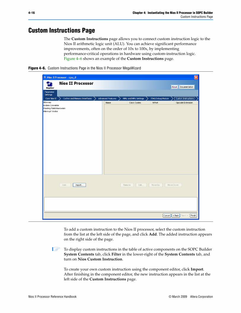
4–16 Chapter 4: Instantiating the Nios II Processor in SOPC BuilderCustom Instructions Page
Custom Instructions PageThe Custom Instructions page allows you to connect custom instruction logic to the Nios II arithmetic logic unit (ALU). You can achieve significant performance improvements, often on the order of 10x to 100x, by implementing performance-critical operations in hardware using custom-instruction logic. Figure 4–6 shows an example of the Custom Instructions page.
To add a custom instruction to the Nios II processor, select the custom instruction from the list at the left side of the page, and click Add. The added instruction appears on the right side of the page.
1 To display custom instructions in the table of active components on the SOPC Builder System Contents tab, click Filter in the lower-right of the System Contents tab, and turn on Nios Custom Instruction.
To create your own custom instruction using the component editor, click Import. After finishing in the component editor, the new instruction appears in the list at the left side of the Custom Instructions page.
Figure 4–6. Custom Instructions Page in the Nios II Processor MegaWizard
Nios II Processor Reference Handbook © March 2009 Altera CorporationPreliminary
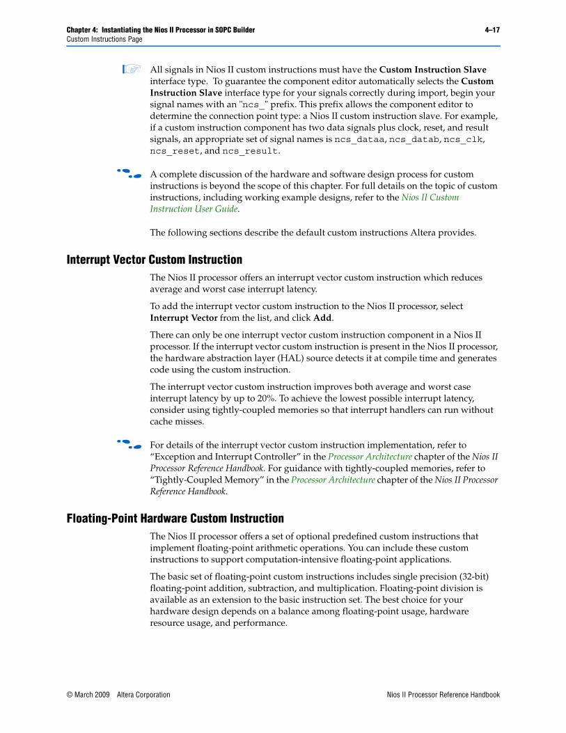
Chapter 4: Instantiating the Nios II Processor in SOPC Builder 4–17Custom Instructions Page
1 All signals in Nios II custom instructions must have the Custom Instruction Slave interface type. To guarantee the component editor automatically selects the Custom Instruction Slave interface type for your signals correctly during import, begin your signal names with an "ncs_" prefix. This prefix allows the component editor to determine the connection point type: a Nios II custom instruction slave. For example, if a custom instruction component has two data signals plus clock, reset, and result signals, an appropriate set of signal names is ncs_dataa, ncs_datab, ncs_clk, ncs_reset, and ncs_result.
f A complete discussion of the hardware and software design process for custom instructions is beyond the scope of this chapter. For full details on the topic of custom instructions, including working example designs, refer to the Nios II Custom Instruction User Guide.
The following sections describe the default custom instructions Altera provides.
Interrupt Vector Custom InstructionThe Nios II processor offers an interrupt vector custom instruction which reduces average and worst case interrupt latency.
To add the interrupt vector custom instruction to the Nios II processor, select Interrupt Vector from the list, and click Add.
There can only be one interrupt vector custom instruction component in a Nios II processor. If the interrupt vector custom instruction is present in the Nios II processor, the hardware abstraction layer (HAL) source detects it at compile time and generates code using the custom instruction.
The interrupt vector custom instruction improves both average and worst case interrupt latency by up to 20%. To achieve the lowest possible interrupt latency, consider using tightly-coupled memories so that interrupt handlers can run without cache misses.
f For details of the interrupt vector custom instruction implementation, refer to “Exception and Interrupt Controller” in the Processor Architecture chapter of the Nios II Processor Reference Handbook. For guidance with tightly-coupled memories, refer to “Tightly-Coupled Memory” in the Processor Architecture chapter of the Nios II Processor Reference Handbook.
Floating-Point Hardware Custom InstructionThe Nios II processor offers a set of optional predefined custom instructions that implement floating-point arithmetic operations. You can include these custom instructions to support computation-intensive floating-point applications.
The basic set of floating-point custom instructions includes single precision (32-bit) floating-point addition, subtraction, and multiplication. Floating-point division is available as an extension to the basic instruction set. The best choice for your hardware design depends on a balance among floating-point usage, hardware resource usage, and performance.
© March 2009 Altera Corporation Nios II Processor Reference HandbookPreliminary
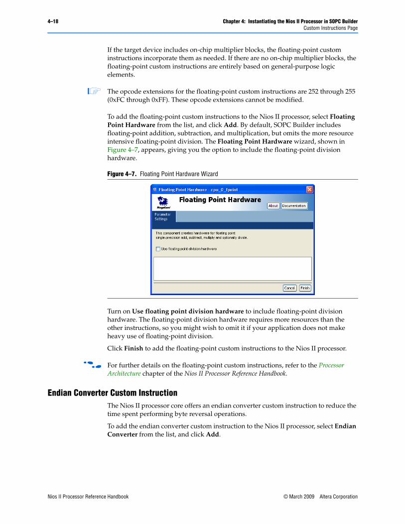
4–18 Chapter 4: Instantiating the Nios II Processor in SOPC BuilderCustom Instructions Page
If the target device includes on-chip multiplier blocks, the floating-point custom instructions incorporate them as needed. If there are no on-chip multiplier blocks, the floating-point custom instructions are entirely based on general-purpose logic elements.
1 The opcode extensions for the floating-point custom instructions are 252 through 255 (0xFC through 0xFF). These opcode extensions cannot be modified.
To add the floating-point custom instructions to the Nios II processor, select Floating Point Hardware from the list, and click Add. By default, SOPC Builder includes floating-point addition, subtraction, and multiplication, but omits the more resource intensive floating-point division. The Floating Point Hardware wizard, shown in Figure 4–7, appears, giving you the option to include the floating-point division hardware.
Turn on Use floating point division hardware to include floating-point division hardware. The floating-point division hardware requires more resources than the other instructions, so you might wish to omit it if your application does not make heavy use of floating-point division.
Click Finish to add the floating-point custom instructions to the Nios II processor.
f For further details on the floating-point custom instructions, refer to the Processor Architecture chapter of the Nios II Processor Reference Handbook.
Endian Converter Custom InstructionThe Nios II processor core offers an endian converter custom instruction to reduce the time spent performing byte reversal operations.
To add the endian converter custom instruction to the Nios II processor, select Endian Converter from the list, and click Add.
Figure 4–7. Floating Point Hardware Wizard
Nios II Processor Reference Handbook © March 2009 Altera CorporationPreliminary
Chapter 4: Instantiating the Nios II Processor in SOPC Builder 4–19The Quartus II IP File
The endian converter custom instruction takes a 32 bit value and converts the endianness in a single clock cycle. The Nios II processor core supports little endian so this custom instruction allows you to convert data shared with a big endian processor core. It is important to note that this custom instruction does not convert the Nios II processor core to big endian architecture, it only converts big endian data to little endian and vice versa.
f For details about integrating the bitswap custom instruction into your own algorithm, refer to the Nios II Custom Instruction User Guide.
Bitswap Custom InstructionThe Nios II processor core offers a bitswap custom instruction to reduce the time spent performing bit reversal operations.
To add the bitswap custom instruction to the Nios II processor, select Bitswap from the list, and click Add.
The bitswap custom instruction reverses a 32 bit value in a single clock cycle. To perform the equivalent operation in software requires many mask and shift operations.
f For details about integrating the bitswap custom instruction into your own algorithm, refer to the Nios II Custom Instruction User Guide.
The Quartus II IP FileThe Quartus II IP file (.qip) is a file generated by the MegaWizard interface or SOPC Builder that contains information about a generated IP core. You are prompted to add this .qip file to the current project at the time of Quartus II file generation. In most cases, the .qip file contains all of the necessary assignments and information required to process the core or system in the Quartus II compiler. Generally, a single .qip file is generated for each MegaCore function and for each SOPC Builder system. However, some more complex SOPC Builder components generate a separate .qip file, so the system .qip file references the component .qip file.
Referenced DocumentsThis chapter references the following documents:
■ Nios II Hardware Development Tutorial
■ Nios II Core Implementation Details chapter of the Nios II Processor Reference Handbook
■ Programming Model chapter of the Nios II Processor Reference Handbook
■ Processor Architecture chapter of the Nios II Processor Reference Handbook
■ Nios II Custom Instruction User Guide
Document Revision HistoryTable 4–3 shows the revision history for this document.
© March 2009 Altera Corporation Nios II Processor Reference HandbookPreliminary
4–20 Chapter 4: Instantiating the Nios II Processor in SOPC BuilderDocument Revision History
Table 4–3. Document Revision History
Date & Document Version Changes Made Summary of Changes
March 2009
v9.0.0
Maintenance release. —
November 2008
v8.1.0
■ Added debugreq and debugack signal options to Advanced Features page.
■ Added cpuid manual override options to Advanced Features page.
—
May 2008
v8.0.0
■ Added MMU options to Nios II Core and Advanced Features pages.
■ Added exception handling options Advanced Features page.
Added MMU and exception handling options.
October 2007
v7.2.0
Changed title to match other Altera documentation. —
May 2007
v7.1.0
■ Revised to reflect new MegaWizard interface.
■ Added “Endian Converter Custom Instruction” on page 4–18 and “Bitswap Custom Instruction” on page 4–19.
■ Added table of contents to Introduction section.
■ Added Referenced Documents section.
—
March 2007
v7.0.0
Maintenance release. —
November 2006
v6.1.0
■ Add section on interrupt vector custom instruction.
■ Add section on system-dependent Nios II processor settings.
—
May 2006
v6.0.0
■ Added details on floating-point custom instructions.
■ Added section on Advanced Features tab.
—
October 2005
v5.1.0
Maintenance release. —
May 2005
v5.0.0
■ Updates to reflect new GUI options in Nios II processor version 5.0.
■ New details in “Caches and Tightly-Coupled Memory” section.
—
September 2004
v1.1
■ Updates to reflect new GUI options in Nios II processor version 1.1.
■ New details in section “Multiply and Divide Settings.”
—
May 2004
v1.0
Initial release. —
Nios II Processor Reference Handbook © March 2009 Altera CorporationPreliminary
© March 2009 Altera Corporation
Section II. Nios II Processor Implementation and Reference
This section provides additional information about the Nios® II processor.
This section includes the following chapters:
■ Chapter 5, Nios II Core Implementation Details
■ Chapter 6, Nios II Processor Revision History
■ Chapter 7, Application Binary Interface
■ Chapter 8, Instruction Set Reference
Nios II Processor Reference HandbookPreliminary

II–2 Section II: Nios II Processor Implementation and Reference
Nios II Processor Reference Handbook © March 2009 Altera CorporationPreliminary
© March 2009 Altera Corporation
NII51015-9.0.0
5. Nios II Core Implementation Details
IntroductionThis document describes all of the Nios® II processor core implementations available at the time of publishing. This document describes only implementation-specific features of each processor core. All cores support the Nios II instruction set architecture.
f For more information regarding the Nios II instruction set architecture, refer to the Instruction Set Reference chapter of the Nios II Processor Reference Handbook.
For common core information and details on a specific core, refer to the appropriate section:
■ “Device Family Support” on page 5–3
■ “Nios II/f Core” on page 5–3
■ “Nios II/s Core” on page 5–12
■ “Nios II/e Core” on page 5–18
Table 5–1 compares the objectives and features of each Nios II processor core. The table is designed to help system designers choose the core that best suits their target application.
Table 5–1. Nios II Processor Cores (Part 1 of 3)
Feature
Core
Nios II/e Nios II/s Nios II/f
Objective Minimal core size Small core size Fast execution speed
Performance DMIPS/MHz (1) 0.15 0.74 1.16
Max. DMIPS (2) 31 127 218
Max. fMAX (2) 200 MHz 165 MHz 185 MHz
Area < 700 LEs;
< 350 ALMs
< 1400 LEs;
< 700 ALMs
Without MMU or MPU:
< 1800 LEs;
< 900 ALMs
With MMU:
< 3000 LEs;
< 1500 ALMs
With MPU:
< 2400 LEs;
< 1200 ALMs
Pipeline 1 stage 5 stages 6 stages
External Address Space 2 GBytes 2 GBytes 2 GBytes without MMU
4 GBytes with MMU
Nios II Processor Reference HandbookPreliminary
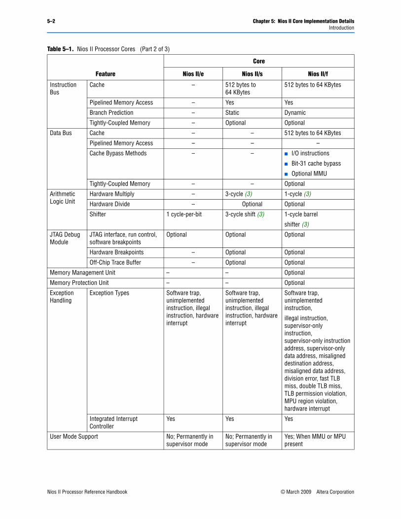
5–2 Chapter 5: Nios II Core Implementation DetailsIntroduction
Instruction Bus
Cache – 512 bytes to 64 KBytes
512 bytes to 64 KBytes
Pipelined Memory Access – Yes Yes
Branch Prediction – Static Dynamic
Tightly-Coupled Memory – Optional Optional
Data Bus Cache – – 512 bytes to 64 KBytes
Pipelined Memory Access – – –
Cache Bypass Methods – – ■ I/O instructions
■ Bit-31 cache bypass
■ Optional MMU
Tightly-Coupled Memory – – Optional
Arithmetic Logic Unit
Hardware Multiply – 3-cycle (3) 1-cycle (3)
Hardware Divide – Optional Optional
Shifter 1 cycle-per-bit 3-cycle shift (3) 1-cycle barrel
shifter (3)
JTAG Debug Module
JTAG interface, run control, software breakpoints
Optional Optional Optional
Hardware Breakpoints – Optional Optional
Off-Chip Trace Buffer – Optional Optional
Memory Management Unit – – Optional
Memory Protection Unit – – Optional
Exception Handling
Exception Types Software trap, unimplemented instruction, illegal instruction, hardware interrupt
Software trap, unimplemented instruction, illegal instruction, hardware interrupt
Software trap, unimplemented instruction,
illegal instruction, supervisor-only instruction, supervisor-only instruction address, supervisor-only data address, misaligned destination address, misaligned data address, division error, fast TLB miss, double TLB miss, TLB permission violation, MPU region violation, hardware interrupt
Integrated Interrupt Controller
Yes Yes Yes
User Mode Support No; Permanently in supervisor mode
No; Permanently in supervisor mode
Yes; When MMU or MPU present
Table 5–1. Nios II Processor Cores (Part 2 of 3)
Feature
Core
Nios II/e Nios II/s Nios II/f
Nios II Processor Reference Handbook © March 2009 Altera CorporationPreliminary
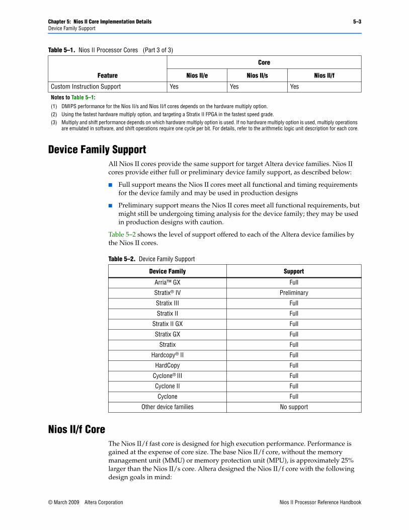
Chapter 5: Nios II Core Implementation Details 5–3Device Family Support
Device Family SupportAll Nios II cores provide the same support for target Altera device families. Nios II cores provide either full or preliminary device family support, as described below:
■ Full support means the Nios II cores meet all functional and timing requirements for the device family and may be used in production designs
■ Preliminary support means the Nios II cores meet all functional requirements, but might still be undergoing timing analysis for the device family; they may be used in production designs with caution.
Table 5–2 shows the level of support offered to each of the Altera device families by the Nios II cores.
Nios II/f CoreThe Nios II/f fast core is designed for high execution performance. Performance is gained at the expense of core size. The base Nios II/f core, without the memory management unit (MMU) or memory protection unit (MPU), is approximately 25% larger than the Nios II/s core. Altera designed the Nios II/f core with the following design goals in mind:
Custom Instruction Support Yes Yes Yes
Notes to Table 5–1:
(1) DMIPS performance for the Nios II/s and Nios II/f cores depends on the hardware multiply option. (2) Using the fastest hardware multiply option, and targeting a Stratix II FPGA in the fastest speed grade.(3) Multiply and shift performance depends on which hardware multiply option is used. If no hardware multiply option is used, multiply operations
are emulated in software, and shift operations require one cycle per bit. For details, refer to the arithmetic logic unit description for each core.
Table 5–1. Nios II Processor Cores (Part 3 of 3)
Feature
Core
Nios II/e Nios II/s Nios II/f
Table 5–2. Device Family Support
Device Family Support
Arria™ GX Full
Stratix® IV Preliminary
Stratix III Full
Stratix II Full
Stratix II GX Full
Stratix GX Full
Stratix Full
Hardcopy® II Full
HardCopy Full
Cyclone® III Full
Cyclone II Full
Cyclone Full
Other device families No support
© March 2009 Altera Corporation Nios II Processor Reference HandbookPreliminary
5–4 Chapter 5: Nios II Core Implementation DetailsNios II/f Core
■ Maximize the instructions-per-cycle execution efficiency
■ Maximize fMAX performance of the processor core
The resulting core is optimal for performance-critical applications, as well as for applications with large amounts of code and/or data, such as systems running a full-featured operating system.
OverviewThe Nios II/f core:
■ Has separate instruction and data caches
■ Provides optional MMU to support operating systems that require an MMU
■ Provides optional MPU to support operating systems and runtime environments that desire memory protection but do not need virtual memory management
■ Can access up to 2 GBytes of external address space when no MMU is present and 4 GBytes when the MMU is present
■ Supports optional tightly-coupled memory for instructions and data
■ Employs a 6-stage pipeline to achieve maximum DMIPS/MHz
■ Performs dynamic branch prediction
■ Provides hardware multiply, divide, and shift options to improve arithmetic performance
■ Supports the addition of custom instructions
■ Supports the JTAG debug module
■ Supports optional JTAG debug module enhancements, including hardware breakpoints and real-time trace
The following sections discuss the noteworthy details of the Nios II/f core implementation. This document does not discuss low-level design issues or implementation details that do not affect Nios II hardware or software designers.
Arithmetic Logic UnitThe Nios II/f core provides several arithmetic logic unit (ALU) options to improve the performance of multiply, divide, and shift operations.
Multiply and Divide PerformanceThe Nios II/f core provides the following hardware multiplier options:
■ DSP Block—Includes DSP block multipliers available on the target device. This option is available only on Altera FPGAs that have DSP Blocks.
■ Embedded Multipliers—Includes dedicated embedded multipliers available on the target device. This option is available only on Altera FPGAs that have embedded multipliers.
■ Logic Elements—Includes hardware multipliers built from logic element (LE) resources.
Nios II Processor Reference Handbook © March 2009 Altera CorporationPreliminary
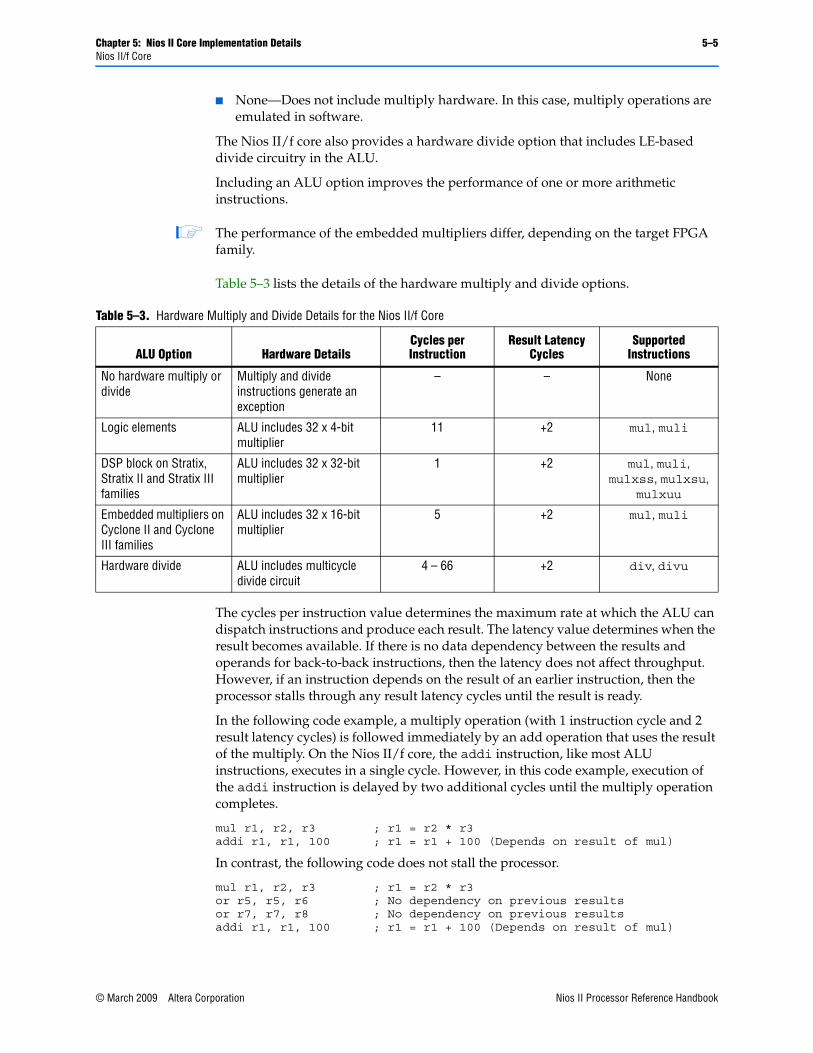
Chapter 5: Nios II Core Implementation Details 5–5Nios II/f Core
■ None—Does not include multiply hardware. In this case, multiply operations are emulated in software.
The Nios II/f core also provides a hardware divide option that includes LE-based divide circuitry in the ALU.
Including an ALU option improves the performance of one or more arithmetic instructions.
1 The performance of the embedded multipliers differ, depending on the target FPGA family.
Table 5–3 lists the details of the hardware multiply and divide options.
The cycles per instruction value determines the maximum rate at which the ALU can dispatch instructions and produce each result. The latency value determines when the result becomes available. If there is no data dependency between the results and operands for back-to-back instructions, then the latency does not affect throughput. However, if an instruction depends on the result of an earlier instruction, then the processor stalls through any result latency cycles until the result is ready.
In the following code example, a multiply operation (with 1 instruction cycle and 2 result latency cycles) is followed immediately by an add operation that uses the result of the multiply. On the Nios II/f core, the addi instruction, like most ALU instructions, executes in a single cycle. However, in this code example, execution of the addi instruction is delayed by two additional cycles until the multiply operation completes.
mul r1, r2, r3 ; r1 = r2 * r3 addi r1, r1, 100 ; r1 = r1 + 100 (Depends on result of mul)
In contrast, the following code does not stall the processor.
mul r1, r2, r3 ; r1 = r2 * r3 or r5, r5, r6 ; No dependency on previous results or r7, r7, r8 ; No dependency on previous results addi r1, r1, 100 ; r1 = r1 + 100 (Depends on result of mul)
Table 5–3. Hardware Multiply and Divide Details for the Nios II/f Core
ALU Option Hardware DetailsCycles per Instruction
Result Latency Cycles
Supported Instructions
No hardware multiply or divide
Multiply and divide instructions generate an exception
– – None
Logic elements ALU includes 32 x 4-bit multiplier
11 +2 mul, muli
DSP block on Stratix, Stratix II and Stratix III families
ALU includes 32 x 32-bit multiplier
1 +2 mul, muli, mulxss, mulxsu,
mulxuu
Embedded multipliers on Cyclone II and Cyclone III families
ALU includes 32 x 16-bit multiplier
5 +2 mul, muli
Hardware divide ALU includes multicycle divide circuit
4 – 66 +2 div, divu
© March 2009 Altera Corporation Nios II Processor Reference HandbookPreliminary
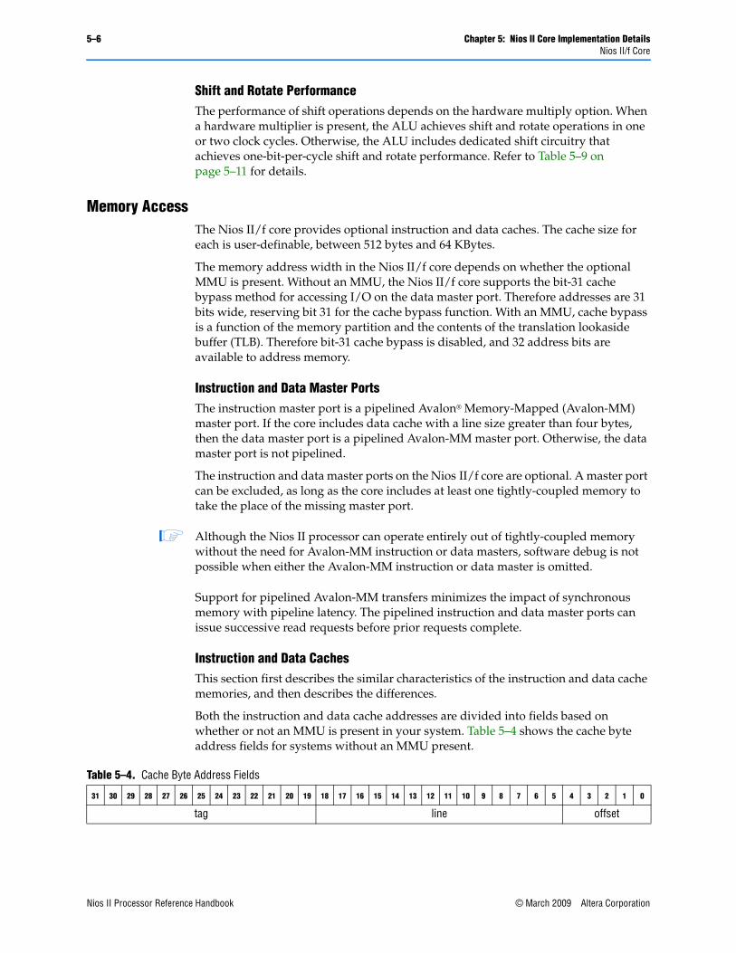
5–6 Chapter 5: Nios II Core Implementation DetailsNios II/f Core
Shift and Rotate PerformanceThe performance of shift operations depends on the hardware multiply option. When a hardware multiplier is present, the ALU achieves shift and rotate operations in one or two clock cycles. Otherwise, the ALU includes dedicated shift circuitry that achieves one-bit-per-cycle shift and rotate performance. Refer to Table 5–9 on page 5–11 for details.
Memory AccessThe Nios II/f core provides optional instruction and data caches. The cache size for each is user-definable, between 512 bytes and 64 KBytes.
The memory address width in the Nios II/f core depends on whether the optional MMU is present. Without an MMU, the Nios II/f core supports the bit-31 cache bypass method for accessing I/O on the data master port. Therefore addresses are 31 bits wide, reserving bit 31 for the cache bypass function. With an MMU, cache bypass is a function of the memory partition and the contents of the translation lookaside buffer (TLB). Therefore bit-31 cache bypass is disabled, and 32 address bits are available to address memory.
Instruction and Data Master PortsThe instruction master port is a pipelined Avalon® Memory-Mapped (Avalon-MM) master port. If the core includes data cache with a line size greater than four bytes, then the data master port is a pipelined Avalon-MM master port. Otherwise, the data master port is not pipelined.
The instruction and data master ports on the Nios II/f core are optional. A master port can be excluded, as long as the core includes at least one tightly-coupled memory to take the place of the missing master port.
1 Although the Nios II processor can operate entirely out of tightly-coupled memory without the need for Avalon-MM instruction or data masters, software debug is not possible when either the Avalon-MM instruction or data master is omitted.
Support for pipelined Avalon-MM transfers minimizes the impact of synchronous memory with pipeline latency. The pipelined instruction and data master ports can issue successive read requests before prior requests complete.
Instruction and Data CachesThis section first describes the similar characteristics of the instruction and data cache memories, and then describes the differences.
Both the instruction and data cache addresses are divided into fields based on whether or not an MMU is present in your system. Table 5–4 shows the cache byte address fields for systems without an MMU present.
Table 5–4. Cache Byte Address Fields
31 30 29 28 27 26 25 24 23 22 21 20 19 18 17 16 15 14 13 12 11 10 9 8 7 6 5 4 3 2 1 0
tag line offset
Nios II Processor Reference Handbook © March 2009 Altera CorporationPreliminary
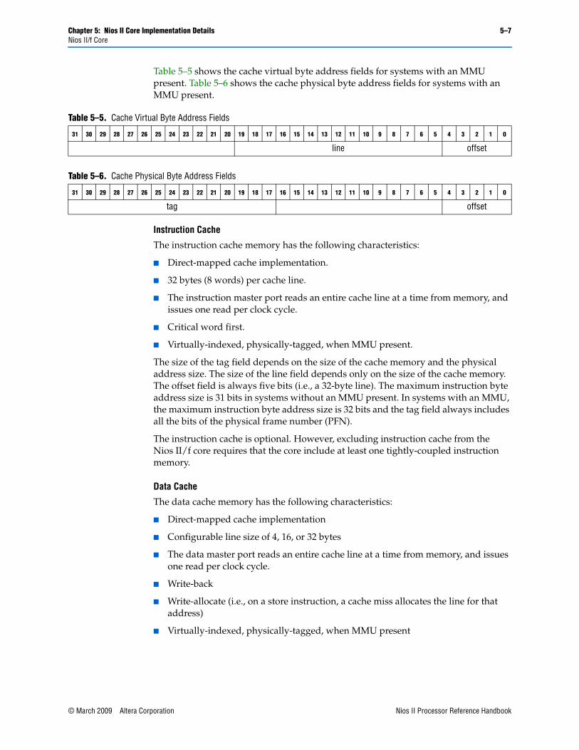
Chapter 5: Nios II Core Implementation Details 5–7Nios II/f Core
Table 5–5 shows the cache virtual byte address fields for systems with an MMU present. Table 5–6 shows the cache physical byte address fields for systems with an MMU present.
Instruction Cache
The instruction cache memory has the following characteristics:
■ Direct-mapped cache implementation.
■ 32 bytes (8 words) per cache line.
■ The instruction master port reads an entire cache line at a time from memory, and issues one read per clock cycle.
■ Critical word first.
■ Virtually-indexed, physically-tagged, when MMU present.
The size of the tag field depends on the size of the cache memory and the physical address size. The size of the line field depends only on the size of the cache memory. The offset field is always five bits (i.e., a 32-byte line). The maximum instruction byte address size is 31 bits in systems without an MMU present. In systems with an MMU, the maximum instruction byte address size is 32 bits and the tag field always includes all the bits of the physical frame number (PFN).
The instruction cache is optional. However, excluding instruction cache from the Nios II/f core requires that the core include at least one tightly-coupled instruction memory.
Data Cache
The data cache memory has the following characteristics:
■ Direct-mapped cache implementation
■ Configurable line size of 4, 16, or 32 bytes
■ The data master port reads an entire cache line at a time from memory, and issues one read per clock cycle.
■ Write-back
■ Write-allocate (i.e., on a store instruction, a cache miss allocates the line for that address)
■ Virtually-indexed, physically-tagged, when MMU present
Table 5–5. Cache Virtual Byte Address Fields
31 30 29 28 27 26 25 24 23 22 21 20 19 18 17 16 15 14 13 12 11 10 9 8 7 6 5 4 3 2 1 0
line offset
Table 5–6. Cache Physical Byte Address Fields
31 30 29 28 27 26 25 24 23 22 21 20 19 18 17 16 15 14 13 12 11 10 9 8 7 6 5 4 3 2 1 0
tag offset
© March 2009 Altera Corporation Nios II Processor Reference HandbookPreliminary
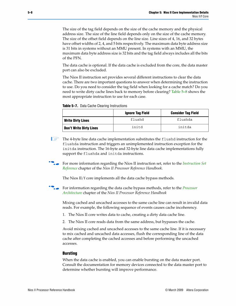
5–8 Chapter 5: Nios II Core Implementation DetailsNios II/f Core
The size of the tag field depends on the size of the cache memory and the physical address size. The size of the line field depends only on the size of the cache memory. The size of the offset field depends on the line size. Line sizes of 4, 16, and 32 bytes have offset widths of 2, 4, and 5 bits respectively. The maximum data byte address size is 31 bits in systems without an MMU present. In systems with an MMU, the maximum data byte address size is 32 bits and the tag field always includes all the bits of the PFN.
The data cache is optional. If the data cache is excluded from the core, the data master port can also be excluded.
The Nios II instruction set provides several different instructions to clear the data cache. There are two important questions to answer when determining the instruction to use. Do you need to consider the tag field when looking for a cache match? Do you need to write dirty cache lines back to memory before clearing? Table 5–8 shows the most appropriate instruction to use for each case.
1 The 4-byte line data cache implementation substitutes the flushd instruction for the flushda instruction and triggers an unimplemented instruction exception for the initda instruction. The 16-byte and 32-byte line data cache implementations fully support the flushda and initda instructions.
f For more information regarding the Nios II instruction set, refer to the Instruction Set Reference chapter of the Nios II Processor Reference Handbook.
The Nios II/f core implements all the data cache bypass methods.
f For information regarding the data cache bypass methods, refer to the Processor Architecture chapter of the Nios II Processor Reference Handbook
Mixing cached and uncached accesses to the same cache line can result in invalid data reads. For example, the following sequence of events causes cache incoherency.
1. The Nios II core writes data to cache, creating a dirty data cache line.
2. The Nios II core reads data from the same address, but bypasses the cache.
Avoid mixing cached and uncached accesses to the same cache line. If it is necessary to mix cached and uncached data accesses, flush the corresponding line of the data cache after completing the cached accesses and before performing the uncached accesses.
BurstingWhen the data cache is enabled, you can enable bursting on the data master port. Consult the documentation for memory devices connected to the data master port to determine whether bursting will improve performance.
Table 5–7. Data Cache Clearing Instructions
Ignore Tag Field Consider Tag Field
Write Dirty Lines flushd flushda
Don’t Write Dirty Lines initd initda
Nios II Processor Reference Handbook © March 2009 Altera CorporationPreliminary
Chapter 5: Nios II Core Implementation Details 5–9Nios II/f Core
Tightly-Coupled MemoryThe Nios II/f core provides optional tightly-coupled memory interfaces for both instructions and data. A Nios II/f core can use up to four each of instruction and data tightly-coupled memories. When a tightly-coupled memory interface is enabled, the Nios II core includes an additional memory interface master port. Each tightly-coupled memory interface must connect directly to exactly one memory slave port.
When tightly-coupled memory is present, the Nios II core decodes addresses internally to determine if requested instructions or data reside in tightly-coupled memory. If the address resides in tightly-coupled memory, the Nios II core fetches the instruction or data through the tightly-coupled memory interface. Software accesses tightly-coupled memory with the usual load and store instructions, such as ldw or ldwio.
Accessing tightly-coupled memory bypasses cache memory. The processor core functions as if cache were not present for the address span of the tightly-coupled memory. Instructions for managing cache, such as initd and flushd, do not affect the tightly-coupled memory, even if the instruction specifies an address in tightly-coupled memory.
When the MMU is present, tightly-coupled memories are always mapped into the kernel partition and can only be accessed in supervisor mode.
Memory Management UnitThe Nios II/f core provides options to improve the performance of the Nios II MMU.
f For details on the MMU architecture, refer to the Programming Model chapter of the Nios II Processor Reference Handbook.
Micro Translation Lookaside BuffersThe translation lookaside buffer (TLB) consists of one main TLB stored in on-chip RAM and two separate micro TLBs (μTLB) for instructions (μITLB) and data (μDTLB) stored in LE-based registers.
The μTLBs have a configurable number of entries and are fully associative. The default configuration has 6 μDTLB entries and 4 μITLB entries. The hardware chooses the least-recently used μTLB entry when loading a new entry.
The μTLBs are not visible to software. They act as an inclusive cache of the main TLB. The processor firsts look for a hit in the μTLB. If it misses, it then looks for a hit in the main TLB. If the main TLB misses, the processor takes an exception. If the main TLB hits, the TLB entry is copied into the μTLB for future accesses.
The hardware automatically flushes the μTLB on each TLB write operation and on a wrctl to the tlbmisc register in case the process identifier (PID) has changed.
Memory Protection UnitThe Nios II/f core provides options to improve the performance of the Nios II MPU. For details on the MPU architecture, refer to the Programming Model chapter of the Nios II Processor Reference Handbook.
© March 2009 Altera Corporation Nios II Processor Reference HandbookPreliminary
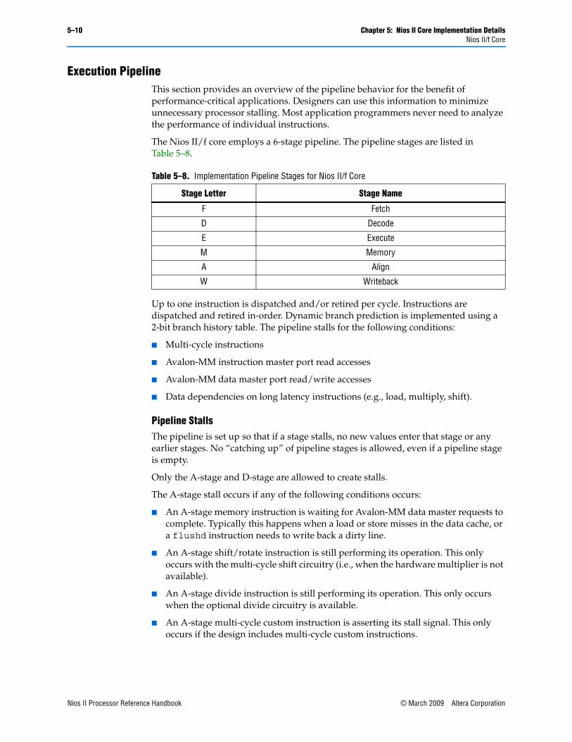
5–10 Chapter 5: Nios II Core Implementation DetailsNios II/f Core
Execution PipelineThis section provides an overview of the pipeline behavior for the benefit of performance-critical applications. Designers can use this information to minimize unnecessary processor stalling. Most application programmers never need to analyze the performance of individual instructions.
The Nios II/f core employs a 6-stage pipeline. The pipeline stages are listed in Table 5–8.
Up to one instruction is dispatched and/or retired per cycle. Instructions are dispatched and retired in-order. Dynamic branch prediction is implemented using a 2-bit branch history table. The pipeline stalls for the following conditions:
■ Multi-cycle instructions
■ Avalon-MM instruction master port read accesses
■ Avalon-MM data master port read/write accesses
■ Data dependencies on long latency instructions (e.g., load, multiply, shift).
Pipeline StallsThe pipeline is set up so that if a stage stalls, no new values enter that stage or any earlier stages. No “catching up” of pipeline stages is allowed, even if a pipeline stage is empty.
Only the A-stage and D-stage are allowed to create stalls.
The A-stage stall occurs if any of the following conditions occurs:
■ An A-stage memory instruction is waiting for Avalon-MM data master requests to complete. Typically this happens when a load or store misses in the data cache, or a flushd instruction needs to write back a dirty line.
■ An A-stage shift/rotate instruction is still performing its operation. This only occurs with the multi-cycle shift circuitry (i.e., when the hardware multiplier is not available).
■ An A-stage divide instruction is still performing its operation. This only occurs when the optional divide circuitry is available.
■ An A-stage multi-cycle custom instruction is asserting its stall signal. This only occurs if the design includes multi-cycle custom instructions.
Table 5–8. Implementation Pipeline Stages for Nios II/f Core
Stage Letter Stage Name
F Fetch
D Decode
E Execute
M Memory
A Align
W Writeback
Nios II Processor Reference Handbook © March 2009 Altera CorporationPreliminary
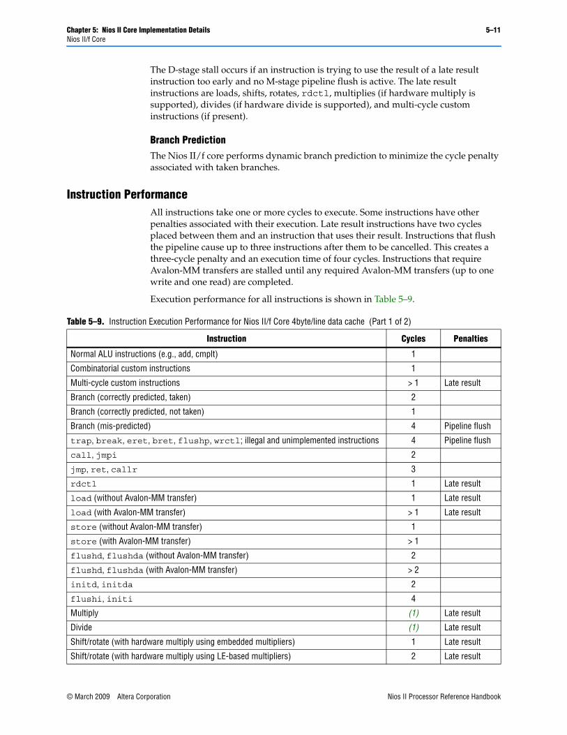
Chapter 5: Nios II Core Implementation Details 5–11Nios II/f Core
The D-stage stall occurs if an instruction is trying to use the result of a late result instruction too early and no M-stage pipeline flush is active. The late result instructions are loads, shifts, rotates, rdctl, multiplies (if hardware multiply is supported), divides (if hardware divide is supported), and multi-cycle custom instructions (if present).
Branch PredictionThe Nios II/f core performs dynamic branch prediction to minimize the cycle penalty associated with taken branches.
Instruction PerformanceAll instructions take one or more cycles to execute. Some instructions have other penalties associated with their execution. Late result instructions have two cycles placed between them and an instruction that uses their result. Instructions that flush the pipeline cause up to three instructions after them to be cancelled. This creates a three-cycle penalty and an execution time of four cycles. Instructions that require Avalon-MM transfers are stalled until any required Avalon-MM transfers (up to one write and one read) are completed.
Execution performance for all instructions is shown in Table 5–9.
Table 5–9. Instruction Execution Performance for Nios II/f Core 4byte/line data cache (Part 1 of 2)
Instruction Cycles Penalties
Normal ALU instructions (e.g., add, cmplt) 1
Combinatorial custom instructions 1
Multi-cycle custom instructions > 1 Late result
Branch (correctly predicted, taken) 2
Branch (correctly predicted, not taken) 1
Branch (mis-predicted) 4 Pipeline flush
trap, break, eret, bret, flushp, wrctl; illegal and unimplemented instructions 4 Pipeline flush
call, jmpi 2
jmp, ret, callr 3
rdctl 1 Late result
load (without Avalon-MM transfer) 1 Late result
load (with Avalon-MM transfer) > 1 Late result
store (without Avalon-MM transfer) 1
store (with Avalon-MM transfer) > 1
flushd, flushda (without Avalon-MM transfer) 2
flushd, flushda (with Avalon-MM transfer) > 2
initd, initda 2
flushi, initi 4
Multiply (1) Late result
Divide (1) Late result
Shift/rotate (with hardware multiply using embedded multipliers) 1 Late result
Shift/rotate (with hardware multiply using LE-based multipliers) 2 Late result
© March 2009 Altera Corporation Nios II Processor Reference HandbookPreliminary
5–12 Chapter 5: Nios II Core Implementation DetailsNios II/s Core
Exception HandlingThe Nios II/f core supports the following exception types:
■ Hardware interrupt
■ Software trap
■ Illegal instruction
■ Unimplemented instruction
■ Supervisor-only instruction
■ Supervisor-only instruction address
■ Supervisor-only data address
■ Misaligned data address
■ Misaligned destination address
■ Division error
■ Fast TLB miss
■ Double TLB miss
■ TLB permission violation
■ MPU region violation
JTAG Debug ModuleThe Nios II/f core supports the JTAG debug module to provide a JTAG interface to software debugging tools. The Nios II/f core supports an optional enhanced interface that allows real-time trace data to be routed out of the processor and stored in an external debug probe.
1 The Nios II MMU does not support the JTAG debug module trace.
Nios II/s CoreThe Nios II/s standard core is designed for small core size. On-chip logic and memory resources are conserved at the expense of execution performance. The Nios II/s core uses approximately 20% less logic than the Nios II/f core, but execution performance also drops by roughly 40%. Altera designed the Nios II/s core with the following design goals in mind:
■ Do not cripple performance for the sake of size.
Shift/rotate (without hardware multiply present) 1 - 32 Late result
All other instructions 1
Note to Table 5–9:
(1) Depends on the hardware multiply or divide option. Refer to Table 5–3 on page 5–5 for details.
Table 5–9. Instruction Execution Performance for Nios II/f Core 4byte/line data cache (Part 2 of 2)
Instruction Cycles Penalties
Nios II Processor Reference Handbook © March 2009 Altera CorporationPreliminary
Chapter 5: Nios II Core Implementation Details 5–13Nios II/s Core
■ Remove hardware features that have the highest ratio of resource usage to performance impact.
The resulting core is optimal for cost-sensitive, medium-performance applications. This includes applications with large amounts of code and/or data, such as systems running an operating system in which performance is not the highest priority.
OverviewThe Nios II/s core:
■ Has an instruction cache, but no data cache
■ Can access up to 2 Gbytes of external address space
■ Supports optional tightly-coupled memory for instructions
■ Employs a 5-stage pipeline
■ Performs static branch prediction
■ Provides hardware multiply, divide, and shift options to improve arithmetic performance
■ Supports the addition of custom instructions
■ Supports the JTAG debug module
■ Supports optional JTAG debug module enhancements, including hardware breakpoints and real-time trace
The following sections discuss the noteworthy details of the Nios II/s core implementation. This document does not discuss low-level design issues or implementation details that do not affect Nios II hardware or software designers.
Arithmetic Logic UnitThe Nios II/s core provides several ALU options to improve the performance of multiply, divide, and shift operations.
Multiply and Divide PerformanceThe Nios II/s core provides the following hardware multiplier options:
■ DSP Block—Includes DSP block multipliers available on the target device. This option is available only on Altera FPGAs that have DSP Blocks.
■ Embedded Multipliers—Includes dedicated embedded multipliers available on the target device. This option is available only on Altera FPGAs that have embedded multipliers.
■ Logic Elements—Includes hardware multipliers built from logic element (LE) resources.
■ None—Does not include multiply hardware. In this case, multiply operations are emulated in software.
The Nios II/s core also provides a hardware divide option that includes LE-based divide circuitry in the ALU.
© March 2009 Altera Corporation Nios II Processor Reference HandbookPreliminary
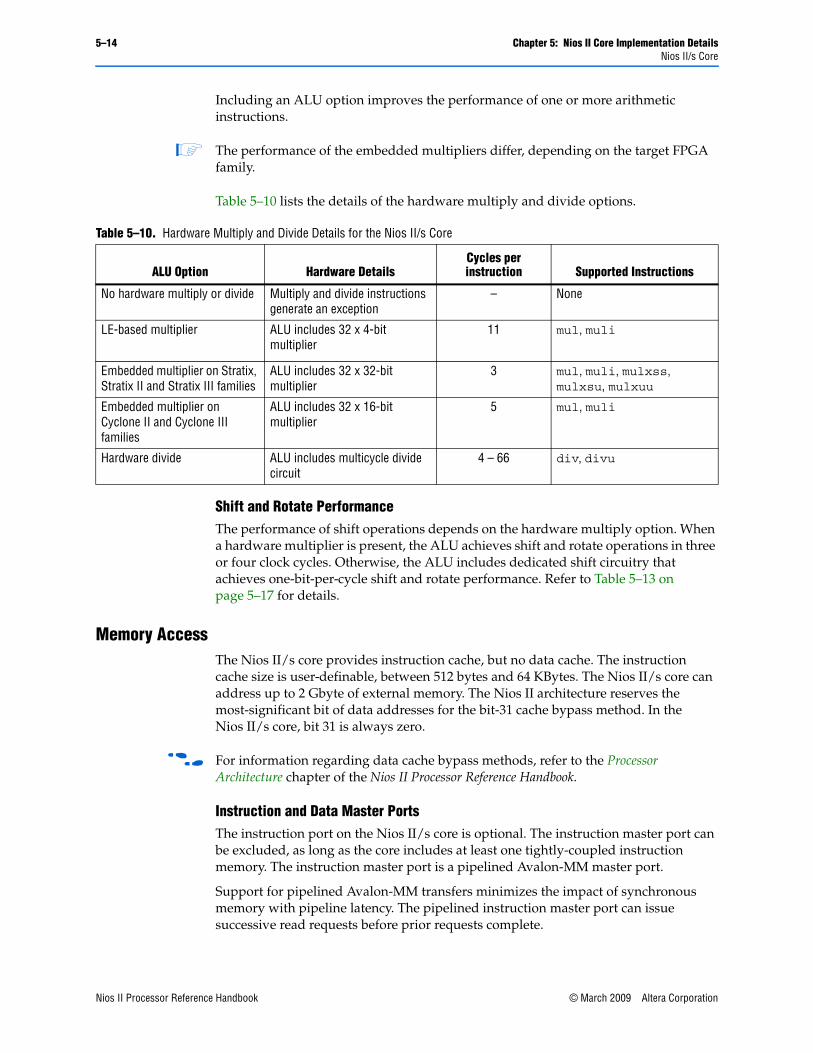
5–14 Chapter 5: Nios II Core Implementation DetailsNios II/s Core
Including an ALU option improves the performance of one or more arithmetic instructions.
1 The performance of the embedded multipliers differ, depending on the target FPGA family.
Table 5–10 lists the details of the hardware multiply and divide options.
Shift and Rotate Performance The performance of shift operations depends on the hardware multiply option. When a hardware multiplier is present, the ALU achieves shift and rotate operations in three or four clock cycles. Otherwise, the ALU includes dedicated shift circuitry that achieves one-bit-per-cycle shift and rotate performance. Refer to Table 5–13 on page 5–17 for details.
Memory AccessThe Nios II/s core provides instruction cache, but no data cache. The instruction cache size is user-definable, between 512 bytes and 64 KBytes. The Nios II/s core can address up to 2 Gbyte of external memory. The Nios II architecture reserves the most-significant bit of data addresses for the bit-31 cache bypass method. In the Nios II/s core, bit 31 is always zero.
f For information regarding data cache bypass methods, refer to the Processor Architecture chapter of the Nios II Processor Reference Handbook.
Instruction and Data Master PortsThe instruction port on the Nios II/s core is optional. The instruction master port can be excluded, as long as the core includes at least one tightly-coupled instruction memory. The instruction master port is a pipelined Avalon-MM master port.
Support for pipelined Avalon-MM transfers minimizes the impact of synchronous memory with pipeline latency. The pipelined instruction master port can issue successive read requests before prior requests complete.
Table 5–10. Hardware Multiply and Divide Details for the Nios II/s Core
ALU Option Hardware DetailsCycles per instruction Supported Instructions
No hardware multiply or divide Multiply and divide instructions generate an exception
– None
LE-based multiplier ALU includes 32 x 4-bit multiplier
11 mul, muli
Embedded multiplier on Stratix, Stratix II and Stratix III families
ALU includes 32 x 32-bit multiplier
3 mul, muli, mulxss, mulxsu, mulxuu
Embedded multiplier on Cyclone II and Cyclone III families
ALU includes 32 x 16-bit multiplier
5 mul, muli
Hardware divide ALU includes multicycle divide circuit
4 – 66 div, divu
Nios II Processor Reference Handbook © March 2009 Altera CorporationPreliminary
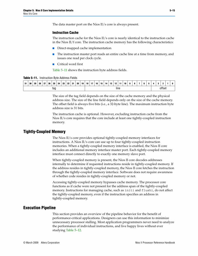
Chapter 5: Nios II Core Implementation Details 5–15Nios II/s Core
The data master port on the Nios II/s core is always present.
Instruction CacheThe instruction cache for the Nios II/s core is nearly identical to the instruction cache in the Nios II/f core. The instruction cache memory has the following characteristics:
■ Direct-mapped cache implementation
■ The instruction master port reads an entire cache line at a time from memory, and issues one read per clock cycle.
■ Critical word first
Table 5–11 shows the instruction byte address fields.
The size of the tag field depends on the size of the cache memory and the physical address size. The size of the line field depends only on the size of the cache memory. The offset field is always five bits (i.e., a 32-byte line). The maximum instruction byte address size is 31 bits.
The instruction cache is optional. However, excluding instruction cache from the Nios II/s core requires that the core include at least one tightly-coupled instruction memory.
Tightly-Coupled MemoryThe Nios II/s core provides optional tightly-coupled memory interfaces for instructions. A Nios II/s core can use up to four tightly-coupled instruction memories. When a tightly-coupled memory interface is enabled, the Nios II core includes an additional memory interface master port. Each tightly-coupled memory interface must connect directly to exactly one memory slave port.
When tightly-coupled memory is present, the Nios II core decodes addresses internally to determine if requested instructions reside in tightly-coupled memory. If the address resides in tightly-coupled memory, the Nios II core fetches the instruction through the tightly-coupled memory interface. Software does not require awareness of whether code resides in tightly-coupled memory or not.
Accessing tightly-coupled memory bypasses cache memory. The processor core functions as if cache were not present for the address span of the tightly-coupled memory. Instructions for managing cache, such as initi and flushi, do not affect the tightly-coupled memory, even if the instruction specifies an address in tightly-coupled memory.
Execution PipelineThis section provides an overview of the pipeline behavior for the benefit of performance-critical applications. Designers can use this information to minimize unnecessary processor stalling. Most application programmers never need to analyze the performance of individual instructions, and live happy lives without ever studying Table 5–12.
Table 5–11. Instruction Byte Address Fields
31 30 29 28 27 26 25 24 23 22 21 20 19 18 17 16 15 14 13 12 11 10 9 8 7 6 5 4 3 2 1 0
tag line offset
© March 2009 Altera Corporation Nios II Processor Reference HandbookPreliminary
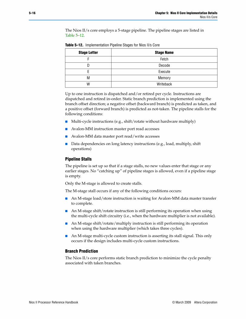
5–16 Chapter 5: Nios II Core Implementation DetailsNios II/s Core
The Nios II/s core employs a 5-stage pipeline. The pipeline stages are listed in Table 5–12.
Up to one instruction is dispatched and/or retired per cycle. Instructions are dispatched and retired in-order. Static branch prediction is implemented using the branch offset direction; a negative offset (backward branch) is predicted as taken, and a positive offset (forward branch) is predicted as not-taken. The pipeline stalls for the following conditions:
■ Multi-cycle instructions (e.g., shift/rotate without hardware multiply)
■ Avalon-MM instruction master port read accesses
■ Avalon-MM data master port read/write accesses
■ Data dependencies on long latency instructions (e.g., load, multiply, shift operations)
Pipeline StallsThe pipeline is set up so that if a stage stalls, no new values enter that stage or any earlier stages. No “catching up” of pipeline stages is allowed, even if a pipeline stage is empty.
Only the M-stage is allowed to create stalls.
The M-stage stall occurs if any of the following conditions occurs:
■ An M-stage load/store instruction is waiting for Avalon-MM data master transfer to complete.
■ An M-stage shift/rotate instruction is still performing its operation when using the multi-cycle shift circuitry (i.e., when the hardware multiplier is not available).
■ An M-stage shift/rotate/multiply instruction is still performing its operation when using the hardware multiplier (which takes three cycles).
■ An M-stage multi-cycle custom instruction is asserting its stall signal. This only occurs if the design includes multi-cycle custom instructions.
Branch PredictionThe Nios II/s core performs static branch prediction to minimize the cycle penalty associated with taken branches.
Table 5–12. Implementation Pipeline Stages for Nios II/s Core
Stage Letter Stage Name
F Fetch
D Decode
E Execute
M Memory
W Writeback
Nios II Processor Reference Handbook © March 2009 Altera CorporationPreliminary
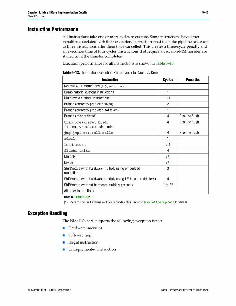
Chapter 5: Nios II Core Implementation Details 5–17Nios II/s Core
Instruction PerformanceAll instructions take one or more cycles to execute. Some instructions have other penalties associated with their execution. Instructions that flush the pipeline cause up to three instructions after them to be cancelled. This creates a three-cycle penalty and an execution time of four cycles. Instructions that require an Avalon-MM transfer are stalled until the transfer completes.
Execution performance for all instructions is shown in Table 5–13.
Exception HandlingThe Nios II/s core supports the following exception types:
■ Hardware interrupt
■ Software trap
■ Illegal instruction
■ Unimplemented instruction
Table 5–13. Instruction Execution Performance for Nios II/s Core
Instruction Cycles Penalties
Normal ALU instructions (e.g., add, cmplt) 1
Combinatorial custom instructions 1
Multi-cycle custom instructions > 1
Branch (correctly predicted taken) 2
Branch (correctly predicted not taken) 1
Branch (mispredicted) 4 Pipeline flush
trap, break, eret, bret, flushp, wrctl, unimplemented
4 Pipeline flush
jmp, jmpi, ret, call, callr 4 Pipeline flush
rdctl 1
load, store > 1
flushi, initi 4
Multiply (1)
Divide (1)
Shift/rotate (with hardware multiply using embedded multipliers)
3
Shift/rotate (with hardware multiply using LE-based multipliers) 4
Shift/rotate (without hardware multiply present) 1 to 32
All other instructions 1
Note to Table 5–13:
(1) Depends on the hardware multiply or divide option. Refer to Table 5–10 on page 5–14 for details.
© March 2009 Altera Corporation Nios II Processor Reference HandbookPreliminary
5–18 Chapter 5: Nios II Core Implementation DetailsNios II/e Core
JTAG Debug ModuleThe Nios II/s core supports the JTAG debug module to provide a JTAG interface to software debugging tools. The Nios II/s core supports an optional enhanced interface that allows real-time trace data to be routed out of the processor and stored in an external debug probe.
Nios II/e CoreThe Nios II/e economy core is designed to achieve the smallest possible core size. Altera designed the Nios II/e core with a singular design goal: reduce resource utilization any way possible, while still maintaining compatibility with the Nios II instruction set architecture. Hardware resources are conserved at the expense of execution performance. The Nios II/e core is roughly half the size of the Nios II/s core, but the execution performance is substantially lower.
The resulting core is optimal for cost-sensitive applications as well as applications that require simple control logic.
OverviewThe Nios II/e core:
■ Executes at most one instruction per six clock cycles
■ Can access up to 2 Gbytes of external address space
■ Supports the addition of custom instructions
■ Supports the JTAG debug module
■ Does not provide hardware support for potential unimplemented instructions
■ Has no instruction cache or data cache
■ Does not perform branch prediction
The following sections discuss the noteworthy details of the Nios II/e core implementation. This document does not discuss low-level design issues, or implementation details that do not affect Nios II hardware or software designers.
Arithmetic Logic UnitThe Nios II/e core does not provide hardware support for any of the potential unimplemented instructions. All unimplemented instructions are emulated in software.
The Nios II/e core employs dedicated shift circuitry to perform shift and rotate operations. The dedicated shift circuitry achieves one-bit-per-cycle shift and rotate operations.
Nios II Processor Reference Handbook © March 2009 Altera CorporationPreliminary
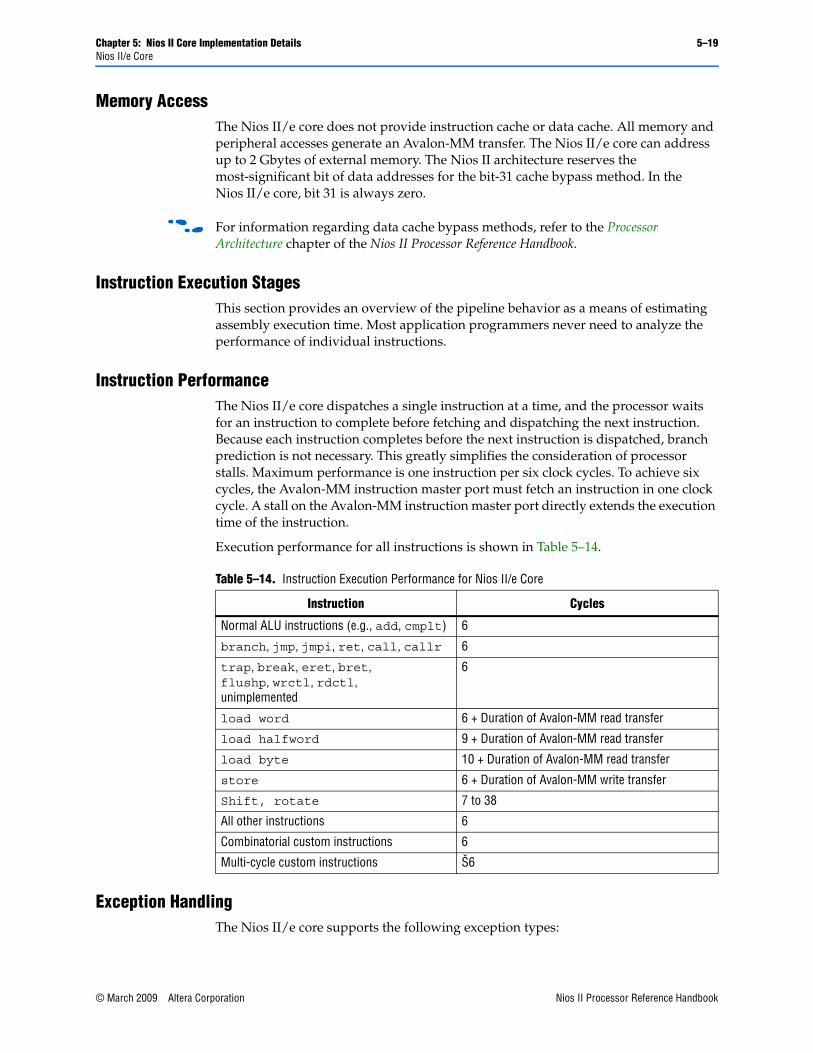
Chapter 5: Nios II Core Implementation Details 5–19Nios II/e Core
Memory AccessThe Nios II/e core does not provide instruction cache or data cache. All memory and peripheral accesses generate an Avalon-MM transfer. The Nios II/e core can address up to 2 Gbytes of external memory. The Nios II architecture reserves the most-significant bit of data addresses for the bit-31 cache bypass method. In the Nios II/e core, bit 31 is always zero.
f For information regarding data cache bypass methods, refer to the Processor Architecture chapter of the Nios II Processor Reference Handbook.
Instruction Execution StagesThis section provides an overview of the pipeline behavior as a means of estimating assembly execution time. Most application programmers never need to analyze the performance of individual instructions.
Instruction PerformanceThe Nios II/e core dispatches a single instruction at a time, and the processor waits for an instruction to complete before fetching and dispatching the next instruction. Because each instruction completes before the next instruction is dispatched, branch prediction is not necessary. This greatly simplifies the consideration of processor stalls. Maximum performance is one instruction per six clock cycles. To achieve six cycles, the Avalon-MM instruction master port must fetch an instruction in one clock cycle. A stall on the Avalon-MM instruction master port directly extends the execution time of the instruction.
Execution performance for all instructions is shown in Table 5–14.
Exception HandlingThe Nios II/e core supports the following exception types:
Table 5–14. Instruction Execution Performance for Nios II/e Core
Instruction Cycles
Normal ALU instructions (e.g., add, cmplt) 6
branch, jmp, jmpi, ret, call, callr 6
trap, break, eret, bret, flushp, wrctl, rdctl, unimplemented
6
load word 6 + Duration of Avalon-MM read transfer
load halfword 9 + Duration of Avalon-MM read transfer
load byte 10 + Duration of Avalon-MM read transfer
store 6 + Duration of Avalon-MM write transfer
Shift, rotate 7 to 38
All other instructions 6
Combinatorial custom instructions 6
Multi-cycle custom instructions Š6
© March 2009 Altera Corporation Nios II Processor Reference HandbookPreliminary
5–20 Chapter 5: Nios II Core Implementation DetailsReferenced Documents
■ Hardware interrupt
■ Software trap
■ Illegal instruction
■ Unimplemented instruction
JTAG Debug ModuleThe Nios II/e core supports the JTAG debug module to provide a JTAG interface to software debugging tools. The JTAG debug module on the Nios II/e core does not support hardware breakpoints or trace.
Referenced DocumentsThis chapter references the following documents:
■ Instruction Set Reference chapter of the Nios II Processor Reference Handbook
■ Processor Architecture chapter of the Nios II Processor Reference Handbook
■ Programming Model chapter of the Nios II Processor Reference Handbook
Document Revision HistoryTable 5–15 shows the revision history for this document.
Table 5–15. Document Revision History (Part 1 of 2)
Date & Document Version Changes Made Summary of Changes
March 2009
v9.0.0
Maintenance release. —
November 2008
v8.1.0
Maintenance release. —
May 2008
v8.0.0
Added text for MMU and MPU. Added MMU and MPU
October 2007
v7.2.0
Added jmpi instruction to tables. —
May 2007
v7.1.0
■ Added table of contents to Introduction section.
■ Added Referenced Documents section.
—
March 2007
v7.0.0
Add preliminary Cyclone III device family support Cyclone III device family
November 2006
v6.1.0
Add preliminary Stratix III device family support Stratix III device family
May 2006
v6.0.0
Performance for flushi and initi instructions changes from 1 to 4 cycles for Nios II/s and Nios II/f cores.
—
October 2005
v5.1.0
Maintenance release. —
Nios II Processor Reference Handbook © March 2009 Altera CorporationPreliminary
Chapter 5: Nios II Core Implementation Details 5–21Document Revision History
May 2005
v5.0.0
Updates to Nios II/f and Nios II/s cores. Added tightly-coupled memory and new data cache options. Corrected cycle counts for shift/rotate operations.
—
December 2004
v1.2
Updates to Multiply and Divide Performance section for Nios II/f and Nios II/s cores.
—
September 2004
v1.1
Updates for Nios II 1.01 release. —
May 2004
v1.0
Initial release. —
Table 5–15. Document Revision History (Part 2 of 2)
Date & Document Version Changes Made Summary of Changes
© March 2009 Altera Corporation Nios II Processor Reference HandbookPreliminary

5–22 Chapter 5: Nios II Core Implementation DetailsDocument Revision History
Nios II Processor Reference Handbook © March 2009 Altera CorporationPreliminary
© March 2009 Altera Corporation
NII51018-9.0.0
6. Nios II Processor Revision History
IntroductionEach release of the Nios® II Embedded Design Suite (EDS) introduces improvements to the Nios II processor, the software development tools, or both. This document catalogs the history of revisions to the Nios II processor; it does not track revisions to development tools, such as the Nios II integrated development environment (IDE). This chapter contains the following sections:
■ “Nios II Versions” on page 6–1
■ “Architecture Revisions” on page 6–2
■ “Core Revisions” on page 6–3
■ “JTAG Debug Module Revisions” on page 6–6
Improvements to the Nios II processor might affect:
■ Features of the Nios II architecture—An example of an architecture revision is adding instructions to support floating-point arithmetic.
■ Implementation of a specific Nios II core—An example of a core revision is increasing the maximum possible size of the data cache memory for the Nios II/f core.
■ Features of the JTAG debug module—An example of a JTAG debug module revision is adding an additional trigger input to the JTAG debug module, allowing it to halt processor execution on a new type of trigger event.
Altera implements Nios II revisions such that code written for an existing Nios II core also works on future revisions of the same core.
Nios II VersionsThe number for any version of the Nios II processor is determined by the version of the Nios II EDS. For example, in the Nios II EDS version 8.0, all Nios II cores are also version 8.0.
Table 6–1 lists the version numbers of all releases of the Nios II processor.
Table 6–1. Nios II Processor Revision History (Part 1 of 2)
Version Release Date Notes
8.0 May 2008 ■ Added an optional memory management unit (MMU).
■ Added an optional memory protection unit (MPU).
■ Added advanced exception checking.
■ Added the initda instruction.
7.2 October 2007 Added the jmpi instruction.
7.1 May 2007 No changes.
7.0 March 2007 No changes.
Nios II Processor Reference HandbookPreliminary
6–2 Chapter 6: Nios II Processor Revision HistoryArchitecture Revisions
Architecture RevisionsArchitecture revisions augment the fundamental capabilities of the Nios II architecture, and affect all Nios II cores. A change in the architecture mandates a revision to all Nios II cores to accommodate the new architectural enhancement. For example, when Altera adds a new instruction to the instruction set, Altera consequently must update all Nios II cores to recognize the new instruction. Table 6–2 lists revisions to the Nios II architecture.
6.1 November 2006 No changes.
6.0 May 2006 The name Nios II Development Kit describing the software development tools changed to Nios II Embedded Design Suite.
5.1 SP1 January 2006 Bug fix for Nios II/f core.
5.1 October 2005 No changes.
5.0 May 2005 ■ Changed version nomenclature. Altera® now aligns the Nios II processor version with Altera's Quartus II® software version.
■ Memory structure enhancements:
(1) Added tightly-coupled memory.
(2) Made data cache line size configurable.
(3) Made cache optional in Nios II/f and Nios II/s cores.
■ Support for HardCopy® devices.
1.1 December 2004 ■ Minor enhancements to the architecture: Added cpuid control register, and updated the break instruction.
■ Increased user control of multiply and shift hardware in the arithmetic logic unit (ALU) for Nios II/s and Nios II/f cores.
■ Minor bug fixes.
1.01 September 2004 ■ Minor bug fixes.
1.0 May2004 Initial release of the Nios II processor.
Table 6–1. Nios II Processor Revision History (Part 2 of 2)
Version Release Date Notes
Table 6–2. Nios II Architecture Revisions (Part 1 of 2)
Version Release Date Notes
8.0 May 2008 ■ Added an optional MMU.
■ Added an optional MPU.
■ Added advanced exception checking to detect division errors, illegal instructions, misaligned memory accesses, and provide extra exception information.
■ Added the initda instruction.
7.2 October 2007 Added the jmpi instruction.
7.1 May 2007 No changes.
7.0 March 2007 No changes.
6.1 November 2006 No changes.
6.0 May 2006 Added optional cpu_resetrequest and cpu_resettaken signals to all processor cores.
Nios II Processor Reference Handbook © March 2009 Altera CorporationPreliminary
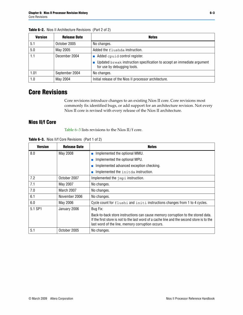
Chapter 6: Nios II Processor Revision History 6–3Core Revisions
Core RevisionsCore revisions introduce changes to an existing Nios II core. Core revisions most commonly fix identified bugs, or add support for an architecture revision. Not every Nios II core is revised with every release of the Nios II architecture.
Nios II/f CoreTable 6–3 lists revisions to the Nios II/f core.
5.1 October 2005 No changes.
5.0 May 2005 Added the flushda instruction.
1.1 December 2004 ■ Added cpuid control register.
■ Updated break instruction specification to accept an immediate argument for use by debugging tools.
1.01 September 2004 No changes.
1.0 May 2004 Initial release of the Nios II processor architecture.
Table 6–2. Nios II Architecture Revisions (Part 2 of 2)
Version Release Date Notes
Table 6–3. Nios II/f Core Revisions (Part 1 of 2)
Version Release Date Notes
8.0 May 2008 ■ Implemented the optional MMU.
■ Implemented the optional MPU.
■ Implemented advanced exception checking.
■ Implemented the initda instruction.
7.2 October 2007 Implemented the jmpi instruction.
7.1 May 2007 No changes.
7.0 March 2007 No changes.
6.1 November 2006 No changes.
6.0 May 2006 Cycle count for flushi and initi instructions changes from 1 to 4 cycles.
5.1 SP1 January 2006 Bug Fix:
Back-to-back store instructions can cause memory corruption to the stored data. If the first store is not to the last word of a cache line and the second store is to the last word of the line, memory corruption occurs.
5.1 October 2005 No changes.
© March 2009 Altera Corporation Nios II Processor Reference HandbookPreliminary
6–4 Chapter 6: Nios II Processor Revision HistoryCore Revisions
Nios II/s CoreTable 6–4 lists revisions to the Nios II/s core.
5.0 May 2005 ■ Added optional tightly-coupled memory ports. Designers can add zero to four tightly-coupled instruction master ports, and zero to four tightly-coupled data master ports.
■ Made the data cache line size configurable. Designers can configure the data cache with the following line sizes: 4, 16, or 32 bytes. Previously, the data cache line size was fixed at 4 bytes.
■ Made instruction and data caches optional (previously, cache memories were always present). If the instruction cache is not present, the Nios II core does not have an instruction master port, and must use a tightly-coupled instruction memory.
■ Full support for HardCopy devices (previous versions required a work around to support HardCopy devices).
1.1 December 2004 ■ Added user-configurable options affecting multiply and shift operations. Now designers can choose one of three options:
(1) Use embedded multiplier resources available in the target device family (previously available).
(2) Use logic elements to implement multiply and shift hardware (new option).
(3) Omit multiply hardware. Shift operations take one cycle per bit shifted; multiply operations are emulated in software (new option).
■ Added cpuid control register.
■ Bug Fix:
Interrupts that were disabled by wrctl ienable remained enabled for one clock cycle following the wrctl instruction. Now the instruction following such a wrctl cannot be interrupted.
1.01 September 2004 ■ Bug Fixes:
(1) When a store to memory is followed immediately in the pipeline by a load from the same memory location, and the memory location is held in the data cache, the load may return invalid data. This situation can occur in C code compiled with optimization off (-O0).
(2) The SOPC Builder top-level system module included an extra, unnecessary output port for systems with very small address spaces.
1.0 May 2004 Initial release of the Nios II/f core.
Table 6–3. Nios II/f Core Revisions (Part 2 of 2)
Version Release Date Notes
Table 6–4. Nios II/s Core Revisions (Part 1 of 2)
Version Release Date Notes
8.0 May 2008 Implemented the illegal instruction exception.
7.2 October 2007 Implemented the jmpi instruction.
7.1 May 2007 No changes.
7.0 March 2007 No changes.
6.1 November 2006 No changes.
6.0 May 2006 Cycle count for flushi and initi instructions changes from 1 to 4 cycles.
Nios II Processor Reference Handbook © March 2009 Altera CorporationPreliminary
Chapter 6: Nios II Processor Revision History 6–5Core Revisions
Nios II/e CoreTable 6–5 lists revisions to the Nios II/e core.
5.1 October 2005 No changes.
5.0 May 2005 ■ Added optional tightly-coupled memory ports. Designers can add zero to four tightly-coupled instruction master ports.
■ Made instruction cache optional (previously instruction cache was always present). If the instruction cache is not present, the Nios II core does not have an instruction master port, and must use a tightly-coupled instruction memory.
■ Full support for HardCopy devices (previous versions required a work around to support HardCopy devices).
1.1 December 2004 ■ Added user-configurable options affecting multiply and shift operations. Now designers can choose one of three options:
(1) Use embedded multiplier resources available in the target device family (previously available).
(2) Use logic elements to implement multiply and shift hardware (new option).
(3) Omit multiply hardware. Shift operations take one cycle per bit shifted; multiply operations are emulated in software (new option).
■ Added user-configurable option to include divide hardware in the ALU. Previously this option was available for only the Nios II/f core.
■ Added cpuid control register.
1.01 September 2004 Bug fix:
The SOPC Builder top-level system module included an extra, unnecessary output port for systems with very small address spaces.
1.0 May 2004 Initial release of the Nios II/s core.
Table 6–4. Nios II/s Core Revisions (Part 2 of 2)
Version Release Date Notes
Table 6–5. Nios II/e Core Revisions
Version Release Date Notes
8.0 May 2008 Implemented the illegal instruction exception.
7.2 October 2007 Implemented the jmpi instruction.
7.1 May 2007 No changes.
7.0 March 2007 No changes.
6.1 November 2006 No changes.
6.0 May 2006 No changes.
5.1 October 2005 No changes.
5.0 May 2005 Full support for HardCopy devices (previous versions required a work around to support HardCopy devices).
1.1 December 2004 Added cpuid control register.
1.01 September 2004 Bug fix:
The SOPC Builder top-level system module included an extra, unnecessary output port for systems with very small address spaces.
1.0 May 2004 Initial release of the Nios II/e core.
© March 2009 Altera Corporation Nios II Processor Reference HandbookPreliminary
6–6 Chapter 6: Nios II Processor Revision HistoryJTAG Debug Module Revisions
JTAG Debug Module RevisionsJTAG debug module revisions augment the debug capabilities of the Nios II processor, or fix bugs isolated within the JTAG debug module logic.
Table 6–6 lists revisions to the JTAG debug module.
Referenced DocumentsThis chapter references no other documents.
Document Revision HistoryTable 6–7 shows the revision history for this document.
Table 6–6. JTAG Debug Module Revisions
Version Release Date Notes
8.0 May 2008 No changes.
7.2 October 2007 No changes.
7.1 May 2007 No changes.
7.0 March 2007 No changes.
6.1 November 2006 No changes.
6.0 May 2006 No changes.
5.1 October 2005 No changes.
5.0 May 2005 Full support for HardCopy devices (previous versions of the JTAG debug module did not support HardCopy devices).
1.1 December 2004 Bug fix:
When using the Nios II/s and Nios II/f cores, hardware breakpoints may have falsely triggered when placed on the instruction sequentially following a jmp, trap, or any branch instruction.
1.01 September 2004 ■ Feature enhancements:
(1) Added the ability to trigger based on the instruction address. Uses include triggering trace control (trace on/off), sequential triggers, and trigger in/out signal generation.
(2) Enhanced trace collection such that collection can be stopped when the trace buffer is full without halting the Nios II processor.
(3) Armed triggers – Enhanced trigger logic to support two levels of triggers, or "armed triggers"; enabling the use of "Event A then event B" trigger definitions.
■ Bug fixes:
(1) On the Nios II/s core, trace data sometimes recorded incorrect addresses during interrupt processing.
(2) Under certain circumstances, captured trace data appeared to start earlier or later than the desired trigger location.
(3) During debugging, the processor would hang if a hardware breakpoint and an interrupt occurred simultaneously.
1.0 May 2004 Initial release of the JTAG debug module.
Nios II Processor Reference Handbook © March 2009 Altera CorporationPreliminary
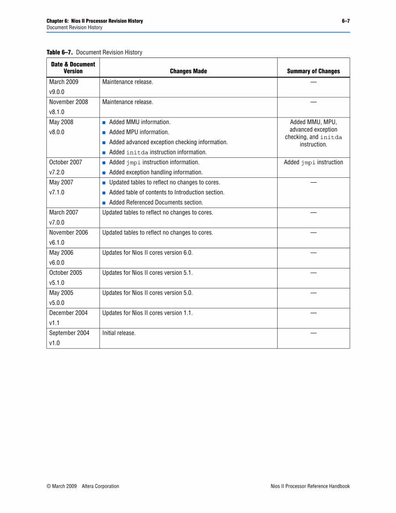
Chapter 6: Nios II Processor Revision History 6–7Document Revision History
Table 6–7. Document Revision History
Date & Document Version Changes Made Summary of Changes
March 2009
v9.0.0
Maintenance release. —
November 2008
v8.1.0
Maintenance release. —
May 2008
v8.0.0
■ Added MMU information.
■ Added MPU information.
■ Added advanced exception checking information.
■ Added initda instruction information.
Added MMU, MPU, advanced exception
checking, and initda instruction.
October 2007
v7.2.0
■ Added jmpi instruction information.
■ Added exception handling information.
Added jmpi instruction
May 2007
v7.1.0
■ Updated tables to reflect no changes to cores.
■ Added table of contents to Introduction section.
■ Added Referenced Documents section.
—
March 2007
v7.0.0
Updated tables to reflect no changes to cores. —
November 2006
v6.1.0
Updated tables to reflect no changes to cores. —
May 2006
v6.0.0
Updates for Nios II cores version 6.0. —
October 2005
v5.1.0
Updates for Nios II cores version 5.1. —
May 2005
v5.0.0
Updates for Nios II cores version 5.0. —
December 2004
v1.1
Updates for Nios II cores version 1.1. —
September 2004
v1.0
Initial release. —
© March 2009 Altera Corporation Nios II Processor Reference HandbookPreliminary

6–8 Chapter 6: Nios II Processor Revision HistoryDocument Revision History
Nios II Processor Reference Handbook © March 2009 Altera CorporationPreliminary
© March 2009 Altera Corporation
NII51016-9.0.0
7. Application Binary Interface
This chapter describes the Application Binary Interface (ABI) for the Nios® II processor. The ABI describes:
■ How data is arranged in memory
■ Behavior and structure of the stack
■ Function calling conventions
This chapter contains the following sections:
■ “Data Types” on page 7–1
■ “Memory Alignment” on page 7–1
■ “Register Usage” on page 7–2
■ “Stacks” on page 7–3
■ “Arguments and Return Values” on page 7–6
■ “Relocation” on page 7–8
Data TypesTable 7–1 shows the size and representation of the C/C++ data types for the Nios II processor.
Memory AlignmentContents in memory are aligned as follows:
Table 7–1. Representation of Data Types
Type Size (Bytes) Representation
char, signed char 1 two’s complement (ASCII)
unsigned char 1 binary (ASCII)
short, signed short 2 two’s complement
unsigned short 2 binary
int, signed int 4 two’s complement
unsigned int 4 binary
long, signed long 4 two’s complement
unsigned long 4 binary
float 4 IEEE
double 8 IEEE
pointer 4 binary
long long 8 two’s complement
unsigned long long 8 binary
Nios II Processor Reference HandbookPreliminary
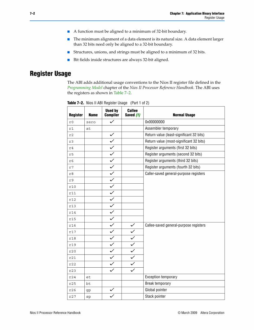
7–2 Chapter 7: Application Binary InterfaceRegister Usage
■ A function must be aligned to a minimum of 32-bit boundary.
■ The minimum alignment of a data element is its natural size. A data element larger than 32 bits need only be aligned to a 32-bit boundary.
■ Structures, unions, and strings must be aligned to a minimum of 32 bits.
■ Bit fields inside structures are always 32-bit aligned.
Register UsageThe ABI adds additional usage conventions to the Nios II register file defined in the Programming Model chapter of the Nios II Processor Reference Handbook. The ABI uses the registers as shown in Table 7–2.
Table 7–2. Nios II ABI Register Usage (Part 1 of 2)
Register NameUsed by Compiler
Callee Saved (1) Normal Usage
r0 zero v 0x00000000
r1 at Assembler temporary
r2 v Return value (least-significant 32 bits)
r3 v Return value (most-significant 32 bits)
r4 v Register arguments (first 32 bits)
r5 v Register arguments (second 32 bits)
r6 v Register arguments (third 32 bits)
r7 v Register arguments (fourth 32 bits)
r8 v Caller-saved general-purpose registers
r9 vr10 vr11 vr12 vr13 vr14 vr15 vr16 v v Callee-saved general-purpose registers
r17 v vr18 v vr19 v vr20 v vr21 v vr22 v vr23 v vr24 et Exception temporary
r25 bt Break temporary
r26 gp v Global pointer
r27 sp v Stack pointer
Nios II Processor Reference Handbook © March 2009 Altera CorporationPreliminary
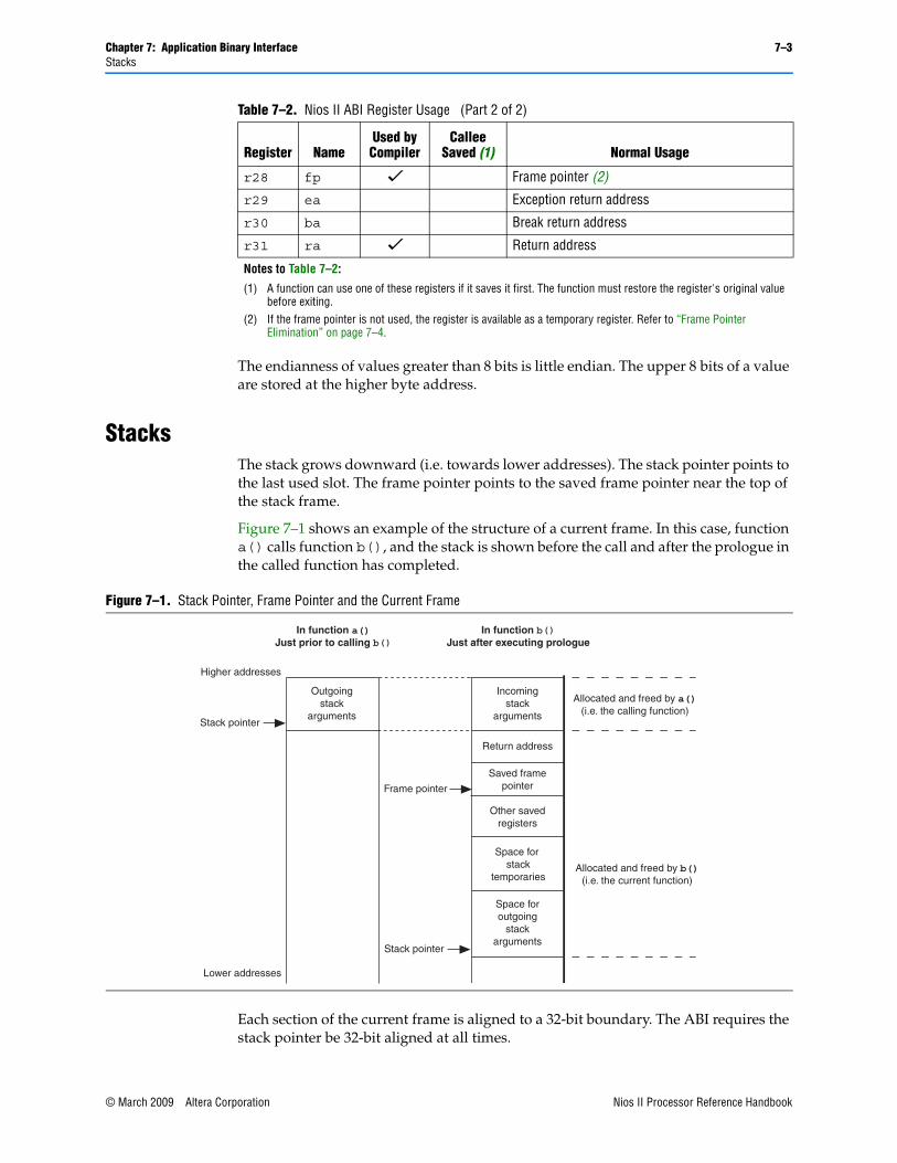
Chapter 7: Application Binary Interface 7–3Stacks
The endianness of values greater than 8 bits is little endian. The upper 8 bits of a value are stored at the higher byte address.
StacksThe stack grows downward (i.e. towards lower addresses). The stack pointer points to the last used slot. The frame pointer points to the saved frame pointer near the top of the stack frame.
Figure 7–1 shows an example of the structure of a current frame. In this case, function a() calls function b(), and the stack is shown before the call and after the prologue in the called function has completed.
Each section of the current frame is aligned to a 32-bit boundary. The ABI requires the stack pointer be 32-bit aligned at all times.
r28 fp v Frame pointer (2)
r29 ea Exception return address
r30 ba Break return address
r31 ra v Return address
Notes to Table 7–2:
(1) A function can use one of these registers if it saves it first. The function must restore the register's original value before exiting.
(2) If the frame pointer is not used, the register is available as a temporary register. Refer to “Frame Pointer Elimination” on page 7–4.
Table 7–2. Nios II ABI Register Usage (Part 2 of 2)
Register NameUsed by Compiler
Callee Saved (1) Normal Usage
Figure 7–1. Stack Pointer, Frame Pointer and the Current Frame
In function a()Just prior to calling b()
In function b()Just after executing prologue
Incomingstack
arguments
Other savedregisters
Space foroutgoing
stackarguments
Allocated and freed by a()(i.e. the calling function)
Allocated and freed by b()(i.e. the current function)
Stack pointer
Outgoingstack
arguments
Higher addresses
Stack pointer
Lower addresses
Space for stack
temporaries
Return address
Saved framepointerFrame pointer
© March 2009 Altera Corporation Nios II Processor Reference HandbookPreliminary
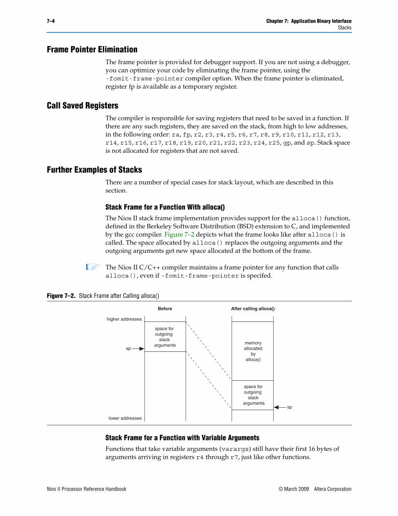
7–4 Chapter 7: Application Binary InterfaceStacks
Frame Pointer EliminationThe frame pointer is provided for debugger support. If you are not using a debugger, you can optimize your code by eliminating the frame pointer, using the -fomit-frame-pointer compiler option. When the frame pointer is eliminated, register fp is available as a temporary register.
Call Saved RegistersThe compiler is responsible for saving registers that need to be saved in a function. If there are any such registers, they are saved on the stack, from high to low addresses, in the following order: ra, fp, r2, r3, r4, r5, r6, r7, r8, r9, r10, r11, r12, r13, r14, r15, r16, r17, r18, r19, r20, r21, r22, r23, r24, r25, gp, and sp. Stack space is not allocated for registers that are not saved.
Further Examples of StacksThere are a number of special cases for stack layout, which are described in this section.
Stack Frame for a Function With alloca()The Nios II stack frame implementation provides support for the alloca() function, defined in the Berkeley Software Distribution (BSD) extension to C, and implemented by the gcc compiler. Figure 7–2 depicts what the frame looks like after alloca() is called. The space allocated by alloca() replaces the outgoing arguments and the outgoing arguments get new space allocated at the bottom of the frame.
1 The Nios II C/C++ compiler maintains a frame pointer for any function that calls alloca(), even if -fomit-frame-pointer is specifed.
Stack Frame for a Function with Variable ArgumentsFunctions that take variable arguments (varargs) still have their first 16 bytes of arguments arriving in registers r4 through r7, just like other functions.
Figure 7–2. Stack Frame after Calling alloca()
higher addresses
lower addresses
space foroutgoing
stack arguments
sp
sp
space foroutgoing
stack arguments
memoryallocated
byalloca()
Before After calling alloca()
Nios II Processor Reference Handbook © March 2009 Altera CorporationPreliminary
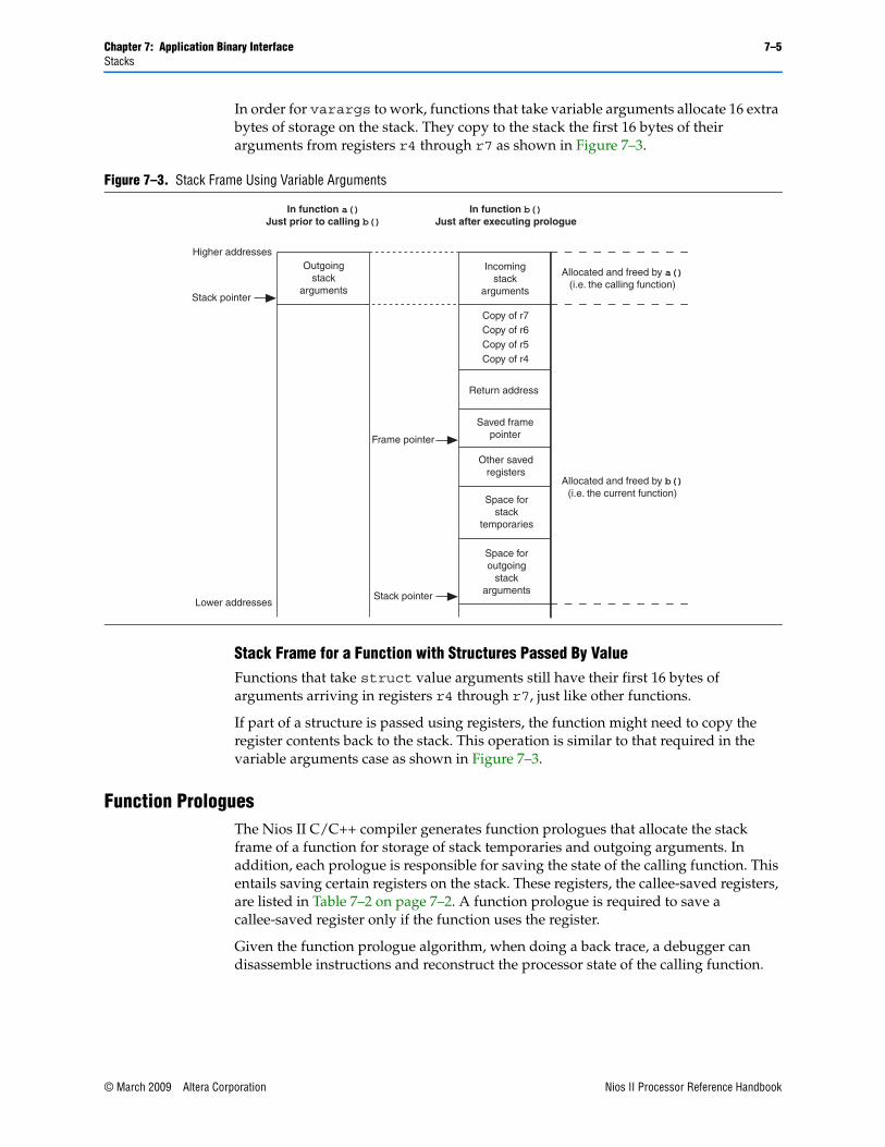
Chapter 7: Application Binary Interface 7–5Stacks
In order for varargs to work, functions that take variable arguments allocate 16 extra bytes of storage on the stack. They copy to the stack the first 16 bytes of their arguments from registers r4 through r7 as shown in Figure 7–3.
Stack Frame for a Function with Structures Passed By ValueFunctions that take struct value arguments still have their first 16 bytes of arguments arriving in registers r4 through r7, just like other functions.
If part of a structure is passed using registers, the function might need to copy the register contents back to the stack. This operation is similar to that required in the variable arguments case as shown in Figure 7–3.
Function ProloguesThe Nios II C/C++ compiler generates function prologues that allocate the stack frame of a function for storage of stack temporaries and outgoing arguments. In addition, each prologue is responsible for saving the state of the calling function. This entails saving certain registers on the stack. These registers, the callee-saved registers, are listed in Table 7–2 on page 7–2. A function prologue is required to save a callee-saved register only if the function uses the register.
Given the function prologue algorithm, when doing a back trace, a debugger can disassemble instructions and reconstruct the processor state of the calling function.
Figure 7–3. Stack Frame Using Variable Arguments
In function a()Just prior to calling b()
In function b()Just after executing prologue
Incomingstack
arguments
Other savedregisters
Space foroutgoing
stackarguments
Allocated and freed by a()(i.e. the calling function)
Allocated and freed by b()(i.e. the current function)
Outgoingstack
arguments
Higher addresses
Lower addresses
Stack pointer
Copy of r7Copy of r6Copy of r5Copy of r4
Space forstack
temporaries
Stack pointer
Return address
Saved framepointerFrame pointer
© March 2009 Altera Corporation Nios II Processor Reference HandbookPreliminary
7–6 Chapter 7: Application Binary InterfaceArguments and Return Values
1 An even better way to find out what the prologue has done is to use information stored in the DWARF2 debugging fields of the executable and linkable format (.elf) file.
The instructions found in a Nios II function prologue perform the following tasks:
■ Adjust the stack pointer (to allocate the frame)
■ Store registers to the frame
■ Set the frame pointer to the location of the saved frame pointer
Example 7–1 shows a function prologue.
Prologue VariationsThe following variations can occur in a prologue:
■ If the function’s frame size is greater than 32,767 bytes, extra temporary registers are used in the calculation of the new stack pointer as well as for the offsets of where to store callee-saved registers. The extra registers are needed because of the maximum size of immediate values allowed by the Nios II processor.
■ If the frame pointer is not in use, the final instruction, recalculating the frame pointer, is not generated.
■ If variable arguments are used, extra instructions store the argument registers on the stack.
■ If the compiler designates the function as a leaf function, the return address is not saved.
■ If optimizations are on, especially instruction scheduling, the order of the instructions might change and become interlaced with instructions located after the prologue.
Arguments and Return ValuesThis section discusses the details of passing arguments to functions and returning values from functions.
Example 7–1. A function prologue
/* Adjust the stack pointer */addi sp, sp, -16 /* make a 16-byte frame */
/* Store registers to the frame */stw ra, 12(sp) /* store the return address */stw fp, 8(sp) /* store the frame pointer*/stw r16, 4(sp) /* store callee-saved register */stw r17, 0(sp) /* store callee-saved register */
/* Set the new frame pointer */addi fp, sp, 8
Nios II Processor Reference Handbook © March 2009 Altera CorporationPreliminary
Chapter 7: Application Binary Interface 7–7Arguments and Return Values
ArgumentsThe first 16 bytes to a function are passed in registers r4 through r7. The arguments are passed as if a structure containing the types of the arguments were constructed, and the first 16 bytes of the structure are located in r4 through r7.
A simple example:
int function (int a, int b);
The equivalent structure representing the arguments is:
struct { int a; int b; };
The first 16 bytes of the struct are assigned to r4 through r7. Therefore r4 is assigned the value of a and r5 the value of b.
The first 16 bytes to a function taking variable arguments are passed the same way as a function not taking variable arguments. The called function must clean up the stack as necessary to support the variable arguments. Refer to “Stack Frame for a Function with Variable Arguments” on page 7–4.
Return ValuesReturn values of types up to 8 bytes are returned in r2 and r3. For return values greater than 8 bytes, the caller must allocate memory for the result and must pass the address of the result memory as a hidden zero argument.
The hidden zero argument is best explained through an example.
In Example 7–2, if the result type is no larger than 8 bytes, b() returns its result in r2 and r3.
If the return type is larger than 8 bytes, the Nios II C/C++ compiler treats this program as if a() had passed a pointer to b(). Example 7–3 shows how the Nios II C/C++ compiler sees the code in Example 7–2.
Example 7–2. Returned struct
/* b() computes a structure-type result and returns it */STRUCT b(int i, int j){
...return result;
}
void a(...){
...value = b(i, j);
}
© March 2009 Altera Corporation Nios II Processor Reference HandbookPreliminary
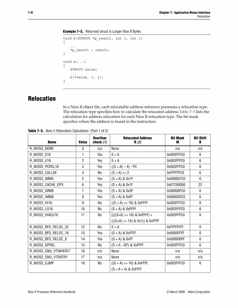
7–8 Chapter 7: Application Binary InterfaceRelocation
RelocationIn a Nios II object file, each relocatable address reference possesses a relocation type. The relocation type specifies how to calculate the relocated address.Table 7–3 lists the calculation for address relocation for each Nios II relocation type. The bit mask specifies where the address is found in the instruction.
Example 7–3. Returned struct is Larger than 8 Bytes
void b(STRUCT *p_result, int i, int j){
...*p_result = result;
}
void a(...){
STRUCT value;...b(*value, i, j);
}
Table 7–3. Nios II Relocation Calculation (Part 1 of 2)
Name ValueOverflowcheck (1)
Relocated AddressR (2)
Bit MaskM
Bit ShiftB
R_NIOS2_NONE 0 n/a None n/a n/a
R_NIOS2_S16 1 Yes S + A 0x003FFFC0 6
R_NIOS2_U16 2 Yes S + A 0x003FFFC0 6
R_NIOS2_PCREL16 3 Yes ((S + A) – 4) - PC 0x003FFFC0 6
R_NIOS2_CALL26 4 No (S + A) >> 2 0xFFFFFFC0 6
R_NIOS2_IMM5 5 Yes (S + A) & 0x1F 0x000007C0 6
R_NIOS2_CACHE_OPX 6 Yes (S + A) & 0x1F 0x07C00000 22
R_NIOS2_IMM6 7 Yes (S + A) & 0x3F 0x00000FC0 6
R_NIOS2_IMM8 8 Yes (S + A) & 0xFF 0x00003FC0 6
R_NIOS2_HI16 9 No ((S + A) >> 16) & 0xFFFF 0x003FFFC0 6
R_NIOS2_LO16 10 No (S + A) & 0xFFFF 0x003FFFC0 6
R_NIOS2_HIADJ16 11 No ((((S+A) >> 16) & 0xFFFF) +
(((S+A) >> 15) & 0x1)) & 0xFFFF
0x003FFFC0 6
R_NIOS2_BFD_RELOC_32 12 No S + A 0xFFFFFFFF 0
R_NIOS2_BFD_RELOC_16 13 Yes (S + A) & 0xFFFF 0x0000FFFF 0
R_NIOS2_BFD_RELOC_8 14 Yes (S + A) & 0xFF 0x000000FF 0
R_NIOS2_GPREL 15 No (S + A - GP) & 0xFFFF 0x003FFFC0 6
R_NIOS2_GNU_VTINHERIT 16 n/a None n/a n/a
R_NIOS2_GNU_VTENTRY 17 n/a None n/a n/a
R_NIOS2_UJMP 18 No ((S + A) >> 16) & 0xFFFF,
(S + A + 4) & 0xFFFF
0x003FFFC0 6
Nios II Processor Reference Handbook © March 2009 Altera CorporationPreliminary
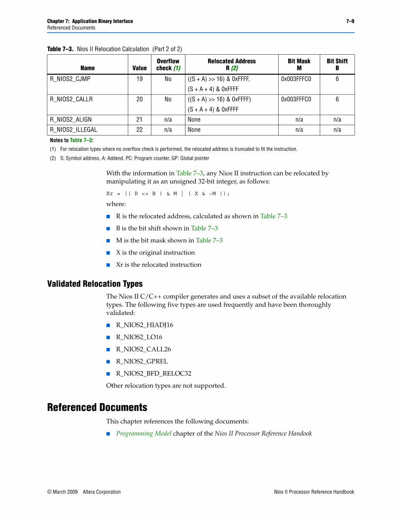
Chapter 7: Application Binary Interface 7–9Referenced Documents
With the information in Table 7–3, any Nios II instruction can be relocated by manipulating it as an unsigned 32-bit integer, as follows:
Xr = (( R << B ) & M | ( X & ~M ));
where:
■ R is the relocated address, calculated as shown in Table 7–3
■ B is the bit shift shown in Table 7–3
■ M is the bit mask shown in Table 7–3
■ X is the original instruction
■ Xr is the relocated instruction
Validated Relocation TypesThe Nios II C/C++ compiler generates and uses a subset of the available relocation types. The following five types are used frequently and have been thoroughly validated:
■ R_NIOS2_HIADJ16
■ R_NIOS2_LO16
■ R_NIOS2_CALL26
■ R_NIOS2_GPREL
■ R_NIOS2_BFD_RELOC32
Other relocation types are not supported.
Referenced DocumentsThis chapter references the following documents:
■ Programming Model chapter of the Nios II Processor Reference Handook
R_NIOS2_CJMP 19 No ((S + A) >> 16) & 0xFFFF,
(S + A + 4) & 0xFFFF
0x003FFFC0 6
R_NIOS2_CALLR 20 No ((S + A) >> 16) & 0xFFFF)
(S + A + 4) & 0xFFFF
0x003FFFC0 6
R_NIOS2_ALIGN 21 n/a None n/a n/a
R_NIOS2_ILLEGAL 22 n/a None n/a n/a
Notes to Table 7–3:
(1) For relocation types where no overflow check is performed, the relocated address is truncated to fit the instruction.
(2) S: Symbol address, A: Addend, PC: Program counter, GP: Global pointer
Table 7–3. Nios II Relocation Calculation (Part 2 of 2)
Name ValueOverflowcheck (1)
Relocated AddressR (2)
Bit MaskM
Bit ShiftB
© March 2009 Altera Corporation Nios II Processor Reference HandbookPreliminary
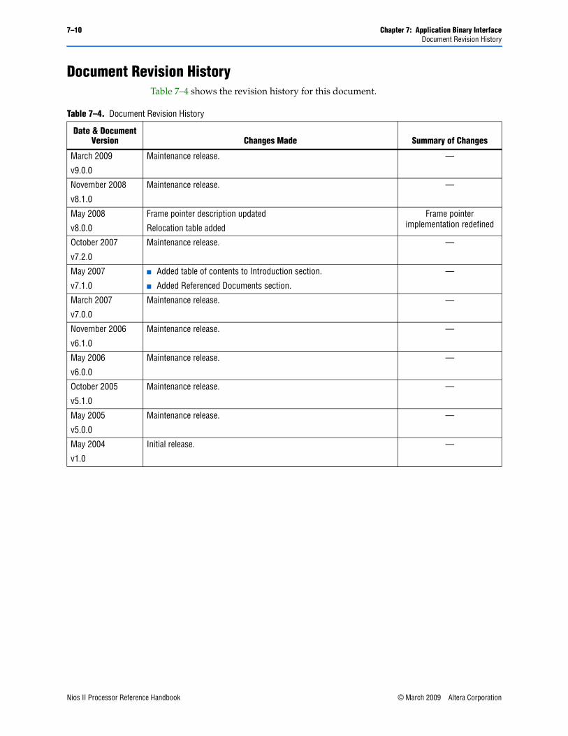
7–10 Chapter 7: Application Binary InterfaceDocument Revision History
Document Revision HistoryTable 7–4 shows the revision history for this document.
Table 7–4. Document Revision History
Date & Document Version Changes Made Summary of Changes
March 2009
v9.0.0
Maintenance release. —
November 2008
v8.1.0
Maintenance release. —
May 2008
v8.0.0
Frame pointer description updated
Relocation table added
Frame pointer implementation redefined
October 2007
v7.2.0
Maintenance release. —
May 2007
v7.1.0
■ Added table of contents to Introduction section.
■ Added Referenced Documents section.
—
March 2007
v7.0.0
Maintenance release. —
November 2006
v6.1.0
Maintenance release. —
May 2006
v6.0.0
Maintenance release. —
October 2005
v5.1.0
Maintenance release. —
May 2005
v5.0.0
Maintenance release. —
May 2004
v1.0
Initial release. —
Nios II Processor Reference Handbook © March 2009 Altera CorporationPreliminary
© March 2009 Altera Corporation
NII51017-9.0.0
8. Instruction Set Reference
IntroductionThis section introduces the Nios® II instruction-word format and provides a detailed reference of the Nios II instruction set. This chapter contains the following sections:
■ “Word Formats” on page 8–1
■ “Instruction Opcodes” on page 8–2
■ “Assembler Pseudo-Instructions” on page 8–3
■ “Assembler Macros” on page 8–4
■ “Instruction Set Reference” on page 8–4
Word FormatsThere are three types of Nios II instruction word format: I-type, R-type, and J-type.
I-TypeThe defining characteristic of the I-type instruction-word format is that it contains an immediate value embedded within the instruction word. I-type instructions words contain:
■ A 6-bit opcode field OP
■ Two 5-bit register fields A and B
■ A 16-bit immediate data field IMM16
In most cases, fields A and IMM16 specify the source operands, and field B specifies the destination register. IMM16 is considered signed except for logical operations and unsigned comparisons.
I-type instructions include arithmetic and logical operations such as addi and andi; branch operations; load and store operations; and cache management operations.
The I-type instruction format is:
R-TypeThe defining characteristic of the R-type instruction-word format is that all arguments and results are specified as registers. R-type instructions contain:
■ A 6-bit opcode field OP
■ Three 5-bit register fields A, B, and C
■ An 11-bit opcode-extension field OPX
31 30 29 28 27 26 25 24 23 22 21 20 19 18 17 16 15 14 13 12 11 10 9 8 7 6 5 4 3 2 1 0
A B IMM16 OP
Nios II Processor Reference HandbookPreliminary
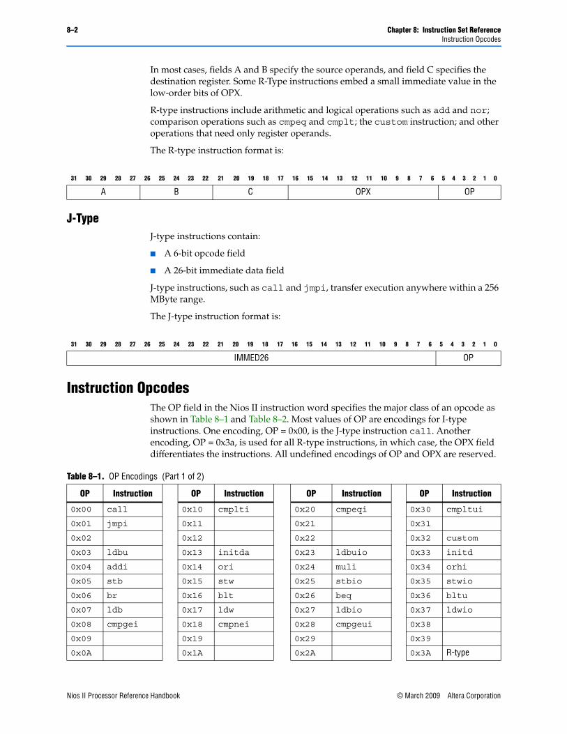
8–2 Chapter 8: Instruction Set ReferenceInstruction Opcodes
In most cases, fields A and B specify the source operands, and field C specifies the destination register. Some R-Type instructions embed a small immediate value in the low-order bits of OPX.
R-type instructions include arithmetic and logical operations such as add and nor; comparison operations such as cmpeq and cmplt; the custom instruction; and other operations that need only register operands.
The R-type instruction format is:
J-TypeJ-type instructions contain:
■ A 6-bit opcode field
■ A 26-bit immediate data field
J-type instructions, such as call and jmpi, transfer execution anywhere within a 256 MByte range.
The J-type instruction format is:
Instruction OpcodesThe OP field in the Nios II instruction word specifies the major class of an opcode as shown in Table 8–1 and Table 8–2. Most values of OP are encodings for I-type instructions. One encoding, OP = 0x00, is the J-type instruction call. Another encoding, OP = 0x3a, is used for all R-type instructions, in which case, the OPX field differentiates the instructions. All undefined encodings of OP and OPX are reserved.
31 30 29 28 27 26 25 24 23 22 21 20 19 18 17 16 15 14 13 12 11 10 9 8 7 6 5 4 3 2 1 0
A B C OPX OP
31 30 29 28 27 26 25 24 23 22 21 20 19 18 17 16 15 14 13 12 11 10 9 8 7 6 5 4 3 2 1 0
IMMED26 OP
Table 8–1. OP Encodings (Part 1 of 2)
OP Instruction OP Instruction OP Instruction OP Instruction
0x00 call 0x10 cmplti 0x20 cmpeqi 0x30 cmpltui
0x01 jmpi 0x11 0x21 0x31
0x02 0x12 0x22 0x32 custom
0x03 ldbu 0x13 initda 0x23 ldbuio 0x33 initd
0x04 addi 0x14 ori 0x24 muli 0x34 orhi
0x05 stb 0x15 stw 0x25 stbio 0x35 stwio
0x06 br 0x16 blt 0x26 beq 0x36 bltu
0x07 ldb 0x17 ldw 0x27 ldbio 0x37 ldwio
0x08 cmpgei 0x18 cmpnei 0x28 cmpgeui 0x38
0x09 0x19 0x29 0x39
0x0A 0x1A 0x2A 0x3A R-type
Nios II Processor Reference Handbook © March 2009 Altera CorporationPreliminary
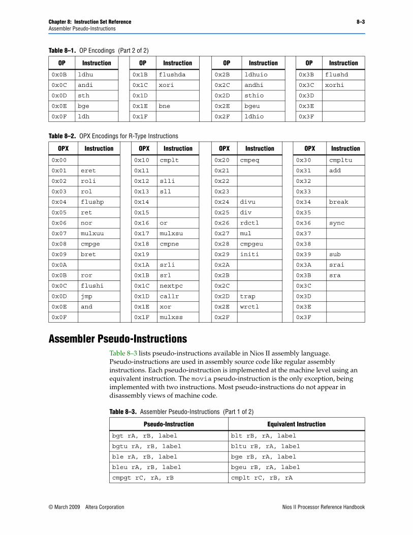
Chapter 8: Instruction Set Reference 8–3Assembler Pseudo-Instructions
Assembler Pseudo-InstructionsTable 8–3 lists pseudo-instructions available in Nios II assembly language. Pseudo-instructions are used in assembly source code like regular assembly instructions. Each pseudo-instruction is implemented at the machine level using an equivalent instruction. The movia pseudo-instruction is the only exception, being implemented with two instructions. Most pseudo-instructions do not appear in disassembly views of machine code.
0x0B ldhu 0x1B flushda 0x2B ldhuio 0x3B flushd
0x0C andi 0x1C xori 0x2C andhi 0x3C xorhi
0x0D sth 0x1D 0x2D sthio 0x3D
0x0E bge 0x1E bne 0x2E bgeu 0x3E
0x0F ldh 0x1F 0x2F ldhio 0x3F
Table 8–2. OPX Encodings for R-Type Instructions
OPX Instruction OPX Instruction OPX Instruction OPX Instruction
0x00 0x10 cmplt 0x20 cmpeq 0x30 cmpltu
0x01 eret 0x11 0x21 0x31 add
0x02 roli 0x12 slli 0x22 0x32
0x03 rol 0x13 sll 0x23 0x33
0x04 flushp 0x14 0x24 divu 0x34 break
0x05 ret 0x15 0x25 div 0x35
0x06 nor 0x16 or 0x26 rdctl 0x36 sync
0x07 mulxuu 0x17 mulxsu 0x27 mul 0x37
0x08 cmpge 0x18 cmpne 0x28 cmpgeu 0x38
0x09 bret 0x19 0x29 initi 0x39 sub
0x0A 0x1A srli 0x2A 0x3A srai
0x0B ror 0x1B srl 0x2B 0x3B sra
0x0C flushi 0x1C nextpc 0x2C 0x3C
0x0D jmp 0x1D callr 0x2D trap 0x3D
0x0E and 0x1E xor 0x2E wrctl 0x3E
0x0F 0x1F mulxss 0x2F 0x3F
Table 8–1. OP Encodings (Part 2 of 2)
OP Instruction OP Instruction OP Instruction OP Instruction
Table 8–3. Assembler Pseudo-Instructions (Part 1 of 2)
Pseudo-Instruction Equivalent Instruction
bgt rA, rB, label blt rB, rA, label
bgtu rA, rB, label bltu rB, rA, label
ble rA, rB, label bge rB, rA, label
bleu rA, rB, label bgeu rB, rA, label
cmpgt rC, rA, rB cmplt rC, rB, rA
© March 2009 Altera Corporation Nios II Processor Reference HandbookPreliminary
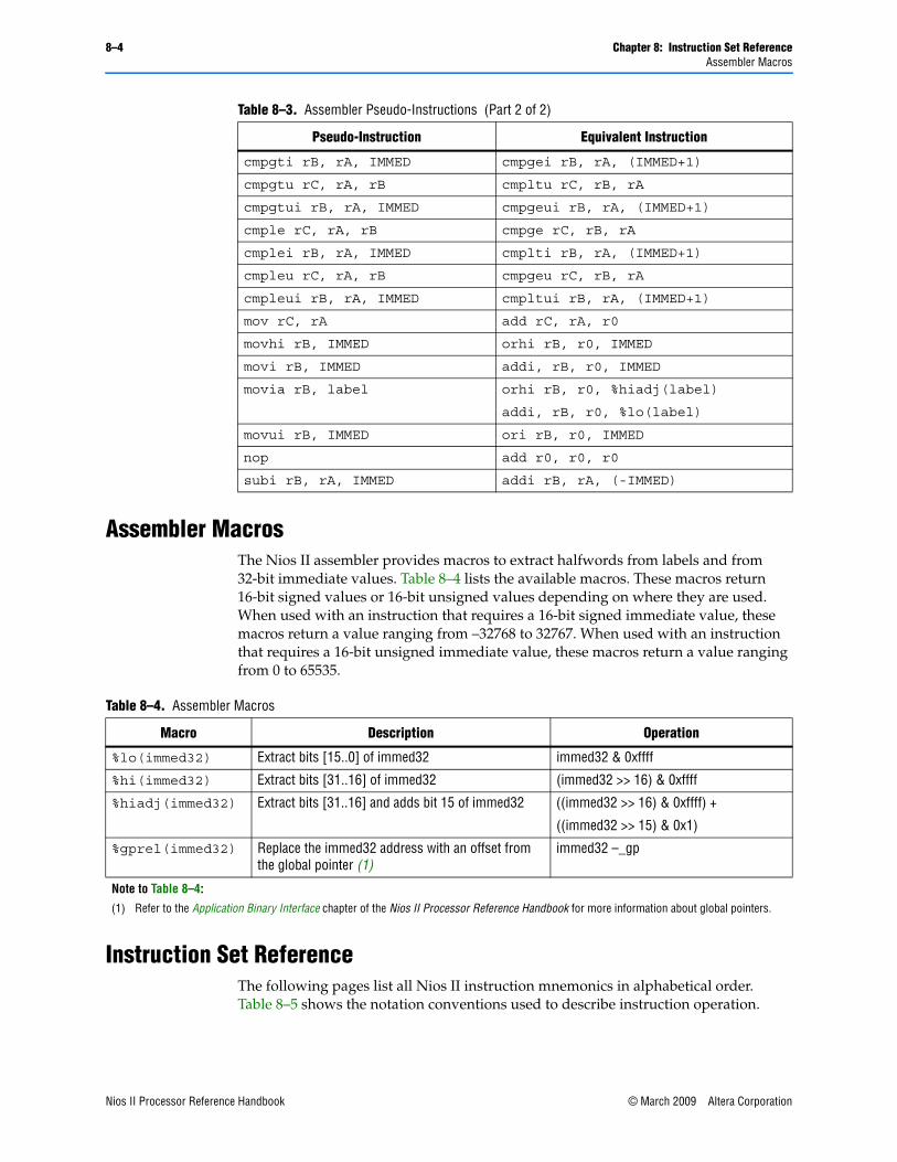
8–4 Chapter 8: Instruction Set ReferenceAssembler Macros
Assembler MacrosThe Nios II assembler provides macros to extract halfwords from labels and from 32-bit immediate values. Table 8–4 lists the available macros. These macros return 16-bit signed values or 16-bit unsigned values depending on where they are used. When used with an instruction that requires a 16-bit signed immediate value, these macros return a value ranging from –32768 to 32767. When used with an instruction that requires a 16-bit unsigned immediate value, these macros return a value ranging from 0 to 65535.
Instruction Set ReferenceThe following pages list all Nios II instruction mnemonics in alphabetical order. Table 8–5 shows the notation conventions used to describe instruction operation.
cmpgti rB, rA, IMMED cmpgei rB, rA, (IMMED+1)
cmpgtu rC, rA, rB cmpltu rC, rB, rA
cmpgtui rB, rA, IMMED cmpgeui rB, rA, (IMMED+1)
cmple rC, rA, rB cmpge rC, rB, rA
cmplei rB, rA, IMMED cmplti rB, rA, (IMMED+1)
cmpleu rC, rA, rB cmpgeu rC, rB, rA
cmpleui rB, rA, IMMED cmpltui rB, rA, (IMMED+1)
mov rC, rA add rC, rA, r0
movhi rB, IMMED orhi rB, r0, IMMED
movi rB, IMMED addi, rB, r0, IMMED
movia rB, label orhi rB, r0, %hiadj(label)
addi, rB, r0, %lo(label)
movui rB, IMMED ori rB, r0, IMMED
nop add r0, r0, r0
subi rB, rA, IMMED addi rB, rA, (-IMMED)
Table 8–3. Assembler Pseudo-Instructions (Part 2 of 2)
Pseudo-Instruction Equivalent Instruction
Table 8–4. Assembler Macros
Macro Description Operation
%lo(immed32) Extract bits [15..0] of immed32 immed32 & 0xffff
%hi(immed32) Extract bits [31..16] of immed32 (immed32 >> 16) & 0xffff
%hiadj(immed32) Extract bits [31..16] and adds bit 15 of immed32 ((immed32 >> 16) & 0xffff) +
((immed32 >> 15) & 0x1)
%gprel(immed32) Replace the immed32 address with an offset from the global pointer (1)
immed32 –_gp
Note to Table 8–4:
(1) Refer to the Application Binary Interface chapter of the Nios II Processor Reference Handbook for more information about global pointers.
Nios II Processor Reference Handbook © March 2009 Altera CorporationPreliminary
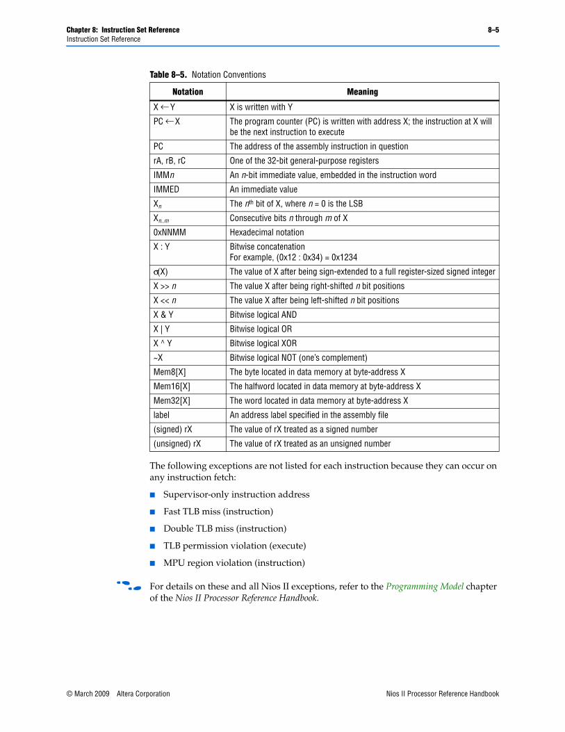
Chapter 8: Instruction Set Reference 8–5Instruction Set Reference
The following exceptions are not listed for each instruction because they can occur on any instruction fetch:
■ Supervisor-only instruction address
■ Fast TLB miss (instruction)
■ Double TLB miss (instruction)
■ TLB permission violation (execute)
■ MPU region violation (instruction)
f For details on these and all Nios II exceptions, refer to the Programming Model chapter of the Nios II Processor Reference Handbook.
Table 8–5. Notation Conventions
Notation Meaning
X ← Y X is written with Y
PC ← X The program counter (PC) is written with address X; the instruction at X will be the next instruction to execute
PC The address of the assembly instruction in question
rA, rB, rC One of the 32-bit general-purpose registers
IMMn An n-bit immediate value, embedded in the instruction word
IMMED An immediate value
Xn The nth bit of X, where n = 0 is the LSB
Xn..m Consecutive bits n through m of X
0xNNMM Hexadecimal notation
X : Y Bitwise concatenation For example, (0x12 : 0x34) = 0x1234
σ(X) The value of X after being sign-extended to a full register-sized signed integer
X >> n The value X after being right-shifted n bit positions
X << n The value X after being left-shifted n bit positions
X & Y Bitwise logical AND
X | Y Bitwise logical OR
X ^ Y Bitwise logical XOR
~X Bitwise logical NOT (one’s complement)
Mem8[X] The byte located in data memory at byte-address X
Mem16[X] The halfword located in data memory at byte-address X
Mem32[X] The word located in data memory at byte-address X
label An address label specified in the assembly file
(signed) rX The value of rX treated as a signed number
(unsigned) rX The value of rX treated as an unsigned number
© March 2009 Altera Corporation Nios II Processor Reference HandbookPreliminary
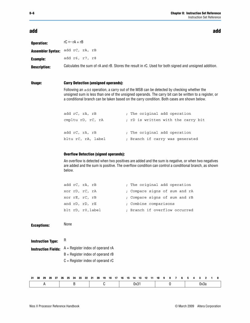
8–6 Chapter 8: Instruction Set ReferenceInstruction Set Reference
add add
Operation: rC ← rA + rB
Assembler Syntax: add rC, rA, rB
Example: add r6, r7, r8
Description: Calculates the sum of rA and rB. Stores the result in rC. Used for both signed and unsigned addition.
Usage: Carry Detection (unsigned operands):
Following an add operation, a carry out of the MSB can be detected by checking whether the unsigned sum is less than one of the unsigned operands. The carry bit can be written to a register, or a conditional branch can be taken based on the carry condition. Both cases are shown below.
add rC, rA, rB
cmpltu rD, rC, rA
add rC, rA, rB
bltu rC, rA, label
; The original add operation
; rD is written with the carry bit
; The original add operation
; Branch if carry was generated
Overflow Detection (signed operands):
An overflow is detected when two positives are added and the sum is negative, or when two negatives are added and the sum is positive. The overflow condition can control a conditional branch, as shown below.
add rC, rA, rB
xor rD, rC, rA
xor rE, rC, rB
and rD, rD, rE
blt rD, r0,label
; The original add operation
; Compare signs of sum and rA
; Compare signs of sum and rB
; Combine comparisons
; Branch if overflow occurred
Exceptions: None
Instruction Type: R
Instruction Fields: A = Register index of operand rA
B = Register index of operand rB
C = Register index of operand rC
31 30 29 28 27 26 25 24 23 22 21 20 19 18 17 16 15 14 13 12 11 10 9 8 7 6 5 4 3 2 1 0
A B C 0x31 0 0x3a
Nios II Processor Reference Handbook © March 2009 Altera CorporationPreliminary
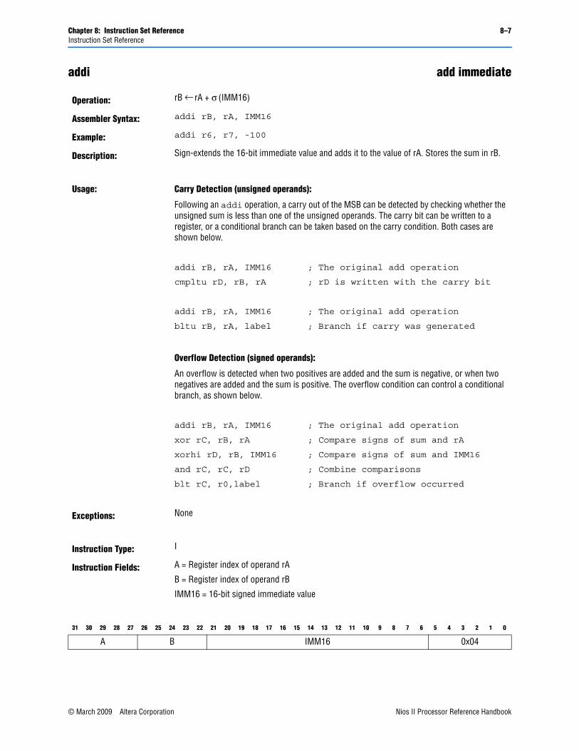
Chapter 8: Instruction Set Reference 8–7Instruction Set Reference
addi add immediate
Operation: rB ← rA + σ (IMM16)
Assembler Syntax: addi rB, rA, IMM16
Example: addi r6, r7, -100
Description: Sign-extends the 16-bit immediate value and adds it to the value of rA. Stores the sum in rB.
Usage: Carry Detection (unsigned operands):
Following an addi operation, a carry out of the MSB can be detected by checking whether the unsigned sum is less than one of the unsigned operands. The carry bit can be written to a register, or a conditional branch can be taken based on the carry condition. Both cases are shown below.
addi rB, rA, IMM16
cmpltu rD, rB, rA
addi rB, rA, IMM16
bltu rB, rA, label
; The original add operation
; rD is written with the carry bit
; The original add operation
; Branch if carry was generated
Overflow Detection (signed operands):
An overflow is detected when two positives are added and the sum is negative, or when two negatives are added and the sum is positive. The overflow condition can control a conditional branch, as shown below.
addi rB, rA, IMM16
xor rC, rB, rA
xorhi rD, rB, IMM16
and rC, rC, rD
blt rC, r0,label
; The original add operation
; Compare signs of sum and rA
; Compare signs of sum and IMM16
; Combine comparisons
; Branch if overflow occurred
Exceptions: None
Instruction Type: I
Instruction Fields: A = Register index of operand rA
B = Register index of operand rB
IMM16 = 16-bit signed immediate value
31 30 29 28 27 26 25 24 23 22 21 20 19 18 17 16 15 14 13 12 11 10 9 8 7 6 5 4 3 2 1 0
A B IMM16 0x04
© March 2009 Altera Corporation Nios II Processor Reference HandbookPreliminary

8–8 Chapter 8: Instruction Set ReferenceInstruction Set Reference
and bitwise logical and
Operation: rC ← rA & rB
Assembler Syntax: and rC, rA, rB
Example: and r6, r7, r8
Description: Calculates the bitwise logical AND of rA and rB and stores the result in rC.
Exceptions: None
Instruction Type: R
Instruction Fields: A = Register index of operand rA
B = Register index of operand rB
C = Register index of operand rC
31 30 29 28 27 26 25 24 23 22 21 20 19 18 17 16 15 14 13 12 11 10 9 8 7 6 5 4 3 2 1 0
A B C 0x0e 0 0x3a
Nios II Processor Reference Handbook © March 2009 Altera CorporationPreliminary
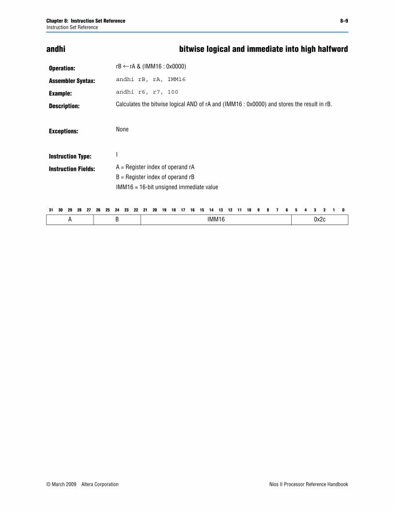
Chapter 8: Instruction Set Reference 8–9Instruction Set Reference
andhi bitwise logical and immediate into high halfword
Operation: rB ← rA & (IMM16 : 0x0000)
Assembler Syntax: andhi rB, rA, IMM16
Example: andhi r6, r7, 100
Description: Calculates the bitwise logical AND of rA and (IMM16 : 0x0000) and stores the result in rB.
Exceptions: None
Instruction Type: I
Instruction Fields: A = Register index of operand rA
B = Register index of operand rB
IMM16 = 16-bit unsigned immediate value
31 30 29 28 27 26 25 24 23 22 21 20 19 18 17 16 15 14 13 12 11 10 9 8 7 6 5 4 3 2 1 0
A B IMM16 0x2c
© March 2009 Altera Corporation Nios II Processor Reference HandbookPreliminary
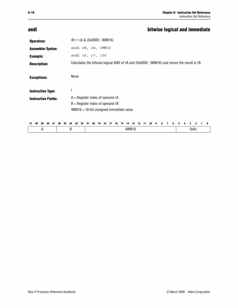
8–10 Chapter 8: Instruction Set ReferenceInstruction Set Reference
andi bitwise logical and immediate
Operation: rB ← rA & (0x0000 : IMM16)
Assembler Syntax: andi rB, rA, IMM16
Example: andi r6, r7, 100
Description: Calculates the bitwise logical AND of rA and (0x0000 : IMM16) and stores the result in rB.
Exceptions: None
Instruction Type: I
Instruction Fields: A = Register index of operand rA
B = Register index of operand rB
IMM16 = 16-bit unsigned immediate value
31 30 29 28 27 26 25 24 23 22 21 20 19 18 17 16 15 14 13 12 11 10 9 8 7 6 5 4 3 2 1 0
A B IMM16 0x0c
Nios II Processor Reference Handbook © March 2009 Altera CorporationPreliminary
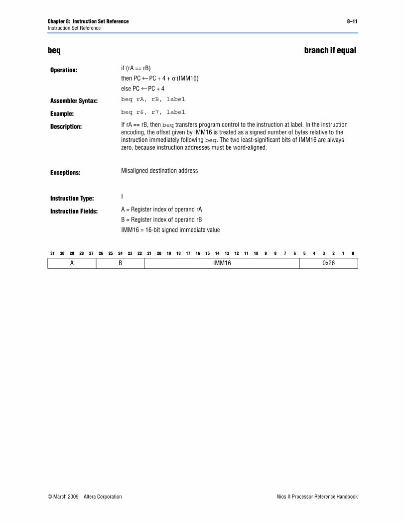
Chapter 8: Instruction Set Reference 8–11Instruction Set Reference
beq branch if equal
Operation: if (rA == rB)
then PC ← PC + 4 + σ (IMM16)
else PC ← PC + 4
Assembler Syntax: beq rA, rB, label
Example: beq r6, r7, label
Description: If rA == rB, then beq transfers program control to the instruction at label. In the instruction encoding, the offset given by IMM16 is treated as a signed number of bytes relative to the instruction immediately following beq. The two least-significant bits of IMM16 are always zero, because instruction addresses must be word-aligned.
Exceptions: Misaligned destination address
Instruction Type: I
Instruction Fields: A = Register index of operand rA
B = Register index of operand rB
IMM16 = 16-bit signed immediate value
31 30 29 28 27 26 25 24 23 22 21 20 19 18 17 16 15 14 13 12 11 10 9 8 7 6 5 4 3 2 1 0
A B IMM16 0x26
© March 2009 Altera Corporation Nios II Processor Reference HandbookPreliminary
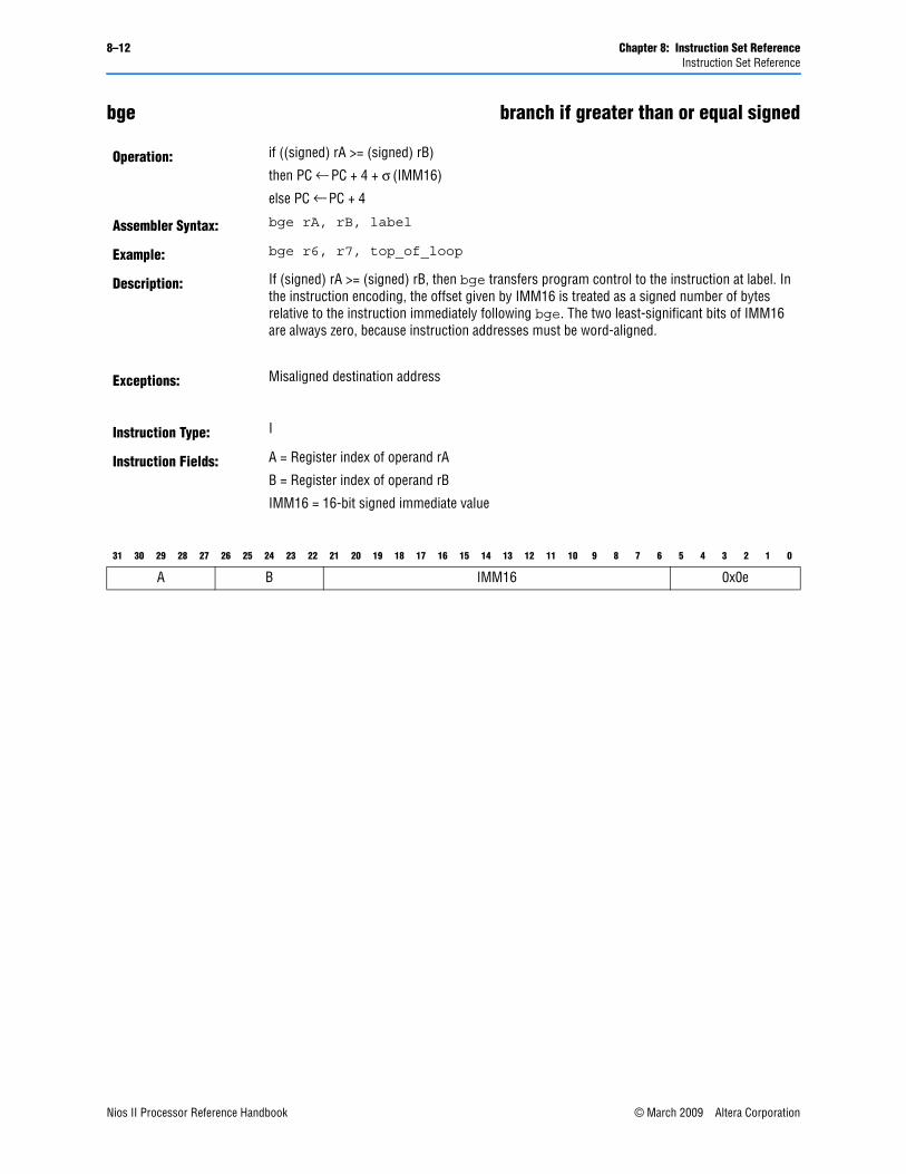
8–12 Chapter 8: Instruction Set ReferenceInstruction Set Reference
bge branch if greater than or equal signed
Operation: if ((signed) rA >= (signed) rB)
then PC ← PC + 4 + σ (IMM16)
else PC ← PC + 4
Assembler Syntax: bge rA, rB, label
Example: bge r6, r7, top_of_loop
Description: If (signed) rA >= (signed) rB, then bge transfers program control to the instruction at label. In the instruction encoding, the offset given by IMM16 is treated as a signed number of bytes relative to the instruction immediately following bge. The two least-significant bits of IMM16 are always zero, because instruction addresses must be word-aligned.
Exceptions: Misaligned destination address
Instruction Type: I
Instruction Fields: A = Register index of operand rA
B = Register index of operand rB
IMM16 = 16-bit signed immediate value
31 30 29 28 27 26 25 24 23 22 21 20 19 18 17 16 15 14 13 12 11 10 9 8 7 6 5 4 3 2 1 0
A B IMM16 0x0e
Nios II Processor Reference Handbook © March 2009 Altera CorporationPreliminary
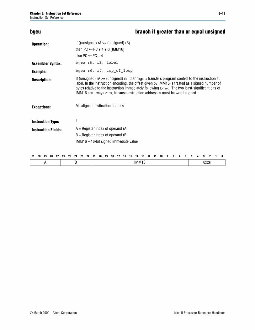
Chapter 8: Instruction Set Reference 8–13Instruction Set Reference
bgeu branch if greater than or equal unsigned
Operation: if ((unsigned) rA >= (unsigned) rB)
then PC ← PC + 4 + σ (IMM16)
else PC ← PC + 4
Assembler Syntax: bgeu rA, rB, label
Example: bgeu r6, r7, top_of_loop
Description: If (unsigned) rA >= (unsigned) rB, then bgeu transfers program control to the instruction at label. In the instruction encoding, the offset given by IMM16 is treated as a signed number of bytes relative to the instruction immediately following bgeu. The two least-significant bits of IMM16 are always zero, because instruction addresses must be word-aligned.
Exceptions: Misaligned destination address
Instruction Type: I
Instruction Fields: A = Register index of operand rA
B = Register index of operand rB
IMM16 = 16-bit signed immediate value
31 30 29 28 27 26 25 24 23 22 21 20 19 18 17 16 15 14 13 12 11 10 9 8 7 6 5 4 3 2 1 0
A B IMM16 0x2e
© March 2009 Altera Corporation Nios II Processor Reference HandbookPreliminary
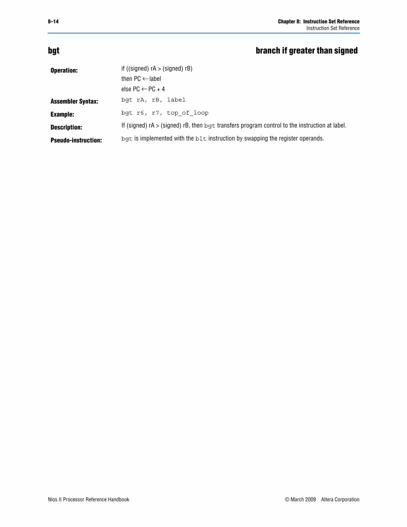
8–14 Chapter 8: Instruction Set ReferenceInstruction Set Reference
bgt branch if greater than signed
Operation: if ((signed) rA > (signed) rB)
then PC ← label
else PC ← PC + 4
Assembler Syntax: bgt rA, rB, label
Example: bgt r6, r7, top_of_loop
Description: If (signed) rA > (signed) rB, then bgt transfers program control to the instruction at label.
Pseudo-instruction: bgt is implemented with the blt instruction by swapping the register operands.
Nios II Processor Reference Handbook © March 2009 Altera CorporationPreliminary
Chapter 8: Instruction Set Reference 8–15Instruction Set Reference
bgtu branch if greater than unsigned
Operation: if ((unsigned) rA > (unsigned) rB)
then PC ← label
else PC ← PC + 4
Assembler Syntax: bgtu rA, rB, label
Example: bgtu r6, r7, top_of_loop
Description: If (unsigned) rA > (unsigned) rB, then bgtu transfers program control to the instruction at label.
Pseudo-instruction: bgtu is implemented with the bltu instruction by swapping the register operands.
© March 2009 Altera Corporation Nios II Processor Reference HandbookPreliminary
8–16 Chapter 8: Instruction Set ReferenceInstruction Set Reference
ble branch if less than or equal signed
Operation: if ((signed) rA <= (signed) rB)
then PC ← label
else PC ← PC + 4
Assembler Syntax: ble rA, rB, label
Example: ble r6, r7, top_of_loop
Description: If (signed) rA <= (signed) rB, then ble transfers program control to the instruction at label.
Pseudo-instruction: ble is implemented with the bge instruction by swapping the register operands.
Nios II Processor Reference Handbook © March 2009 Altera CorporationPreliminary
Chapter 8: Instruction Set Reference 8–17Instruction Set Reference
bleu branch if less than or equal to unsigned
Operation: if ((unsigned) rA <= (unsigned) rB)
then PC ← label
else PC ← PC + 4
Assembler Syntax: bleu rA, rB, label
Example: bleu r6, r7, top_of_loop
Description: If (unsigned) rA <= (unsigned) rB, then bleu transfers program counter to the instruction at label.
Pseudo-instruction: bleu is implemented with the bgeu instruction by swapping the register operands.
© March 2009 Altera Corporation Nios II Processor Reference HandbookPreliminary
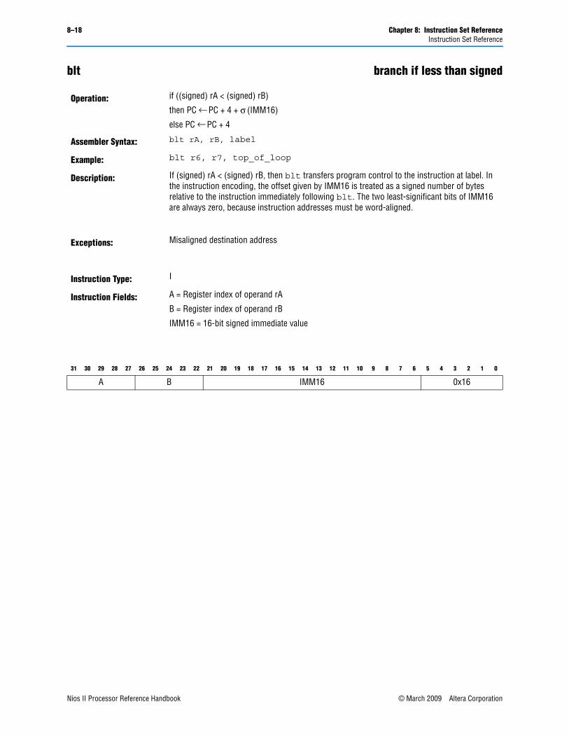
8–18 Chapter 8: Instruction Set ReferenceInstruction Set Reference
blt branch if less than signed
Operation: if ((signed) rA < (signed) rB)
then PC ← PC + 4 + σ (IMM16)
else PC ← PC + 4
Assembler Syntax: blt rA, rB, label
Example: blt r6, r7, top_of_loop
Description: If (signed) rA < (signed) rB, then blt transfers program control to the instruction at label. In the instruction encoding, the offset given by IMM16 is treated as a signed number of bytes relative to the instruction immediately following blt. The two least-significant bits of IMM16 are always zero, because instruction addresses must be word-aligned.
Exceptions: Misaligned destination address
Instruction Type: I
Instruction Fields: A = Register index of operand rA
B = Register index of operand rB
IMM16 = 16-bit signed immediate value
31 30 29 28 27 26 25 24 23 22 21 20 19 18 17 16 15 14 13 12 11 10 9 8 7 6 5 4 3 2 1 0
A B IMM16 0x16
Nios II Processor Reference Handbook © March 2009 Altera CorporationPreliminary
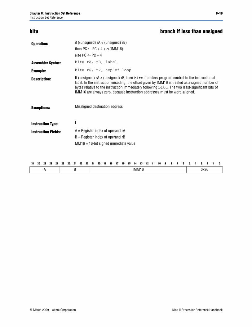
Chapter 8: Instruction Set Reference 8–19Instruction Set Reference
bltu branch if less than unsigned
Operation: if ((unsigned) rA < (unsigned) rB)
then PC ← PC + 4 + σ (IMM16)
else PC ← PC + 4
Assembler Syntax: bltu rA, rB, label
Example: bltu r6, r7, top_of_loop
Description: If (unsigned) rA < (unsigned) rB, then bltu transfers program control to the instruction at label. In the instruction encoding, the offset given by IMM16 is treated as a signed number of bytes relative to the instruction immediately following bltu. The two least-significant bits of IMM16 are always zero, because instruction addresses must be word-aligned.
Exceptions: Misaligned destination address
Instruction Type: I
Instruction Fields: A = Register index of operand rA
B = Register index of operand rB
MM16 = 16-bit signed immediate value
31 30 29 28 27 26 25 24 23 22 21 20 19 18 17 16 15 14 13 12 11 10 9 8 7 6 5 4 3 2 1 0
A B IMM16 0x36
© March 2009 Altera Corporation Nios II Processor Reference HandbookPreliminary
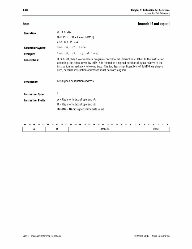
8–20 Chapter 8: Instruction Set ReferenceInstruction Set Reference
bne branch if not equal
Operation: if (rA != rB)
then PC ← PC + 4 + σ (IMM16)
else PC ← PC + 4
Assembler Syntax: bne rA, rB, label
Example: bne r6, r7, top_of_loop
Description: If rA != rB, then bne transfers program control to the instruction at label. In the instruction encoding, the offset given by IMM16 is treated as a signed number of bytes relative to the instruction immediately following bne. The two least-significant bits of IMM16 are always zero, because instruction addresses must be word-aligned.
Exceptions: Misaligned destination address
Instruction Type: I
Instruction Fields: A = Register index of operand rA
B = Register index of operand rB
IMM16 = 16-bit signed immediate value
31 30 29 28 27 26 25 24 23 22 21 20 19 18 17 16 15 14 13 12 11 10 9 8 7 6 5 4 3 2 1 0
A B IMM16 0x1e
Nios II Processor Reference Handbook © March 2009 Altera CorporationPreliminary
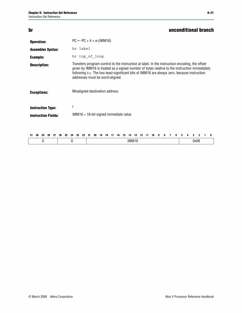
Chapter 8: Instruction Set Reference 8–21Instruction Set Reference
br unconditional branch
Operation: PC ← PC + 4 + σ (IMM16)
Assembler Syntax: br label
Example: br top_of_loop
Description: Transfers program control to the instruction at label. In the instruction encoding, the offset given by IMM16 is treated as a signed number of bytes relative to the instruction immediately following br. The two least-significant bits of IMM16 are always zero, because instruction addresses must be word-aligned.
Exceptions: Misaligned destination address
Instruction Type: I
Instruction Fields: IMM16 = 16-bit signed immediate value
31 30 29 28 27 26 25 24 23 22 21 20 19 18 17 16 15 14 13 12 11 10 9 8 7 6 5 4 3 2 1 0
0 0 IMM16 0x06
© March 2009 Altera Corporation Nios II Processor Reference HandbookPreliminary
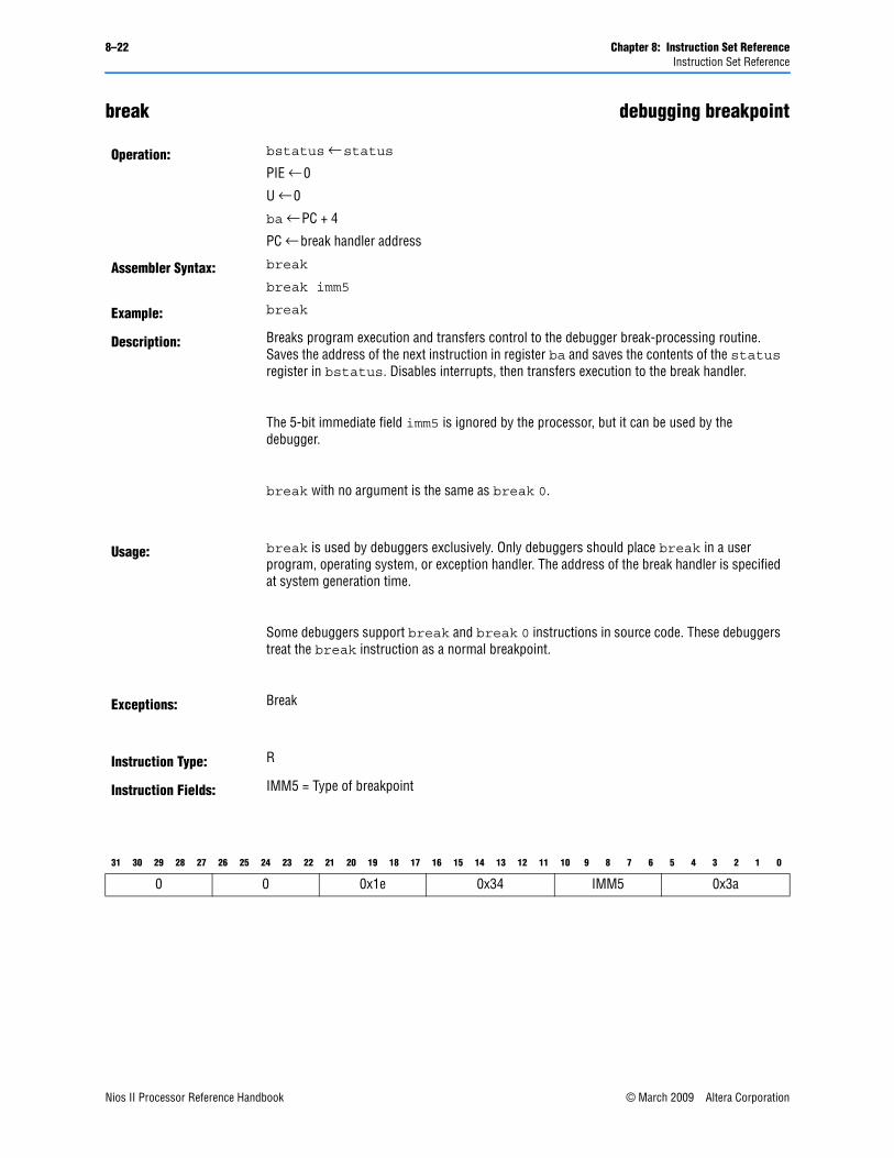
8–22 Chapter 8: Instruction Set ReferenceInstruction Set Reference
break debugging breakpoint
Operation: bstatus ← status
PIE ← 0
U ← 0
ba ← PC + 4
PC ← break handler address
Assembler Syntax: break
break imm5
Example: break
Description: Breaks program execution and transfers control to the debugger break-processing routine. Saves the address of the next instruction in register ba and saves the contents of the status register in bstatus. Disables interrupts, then transfers execution to the break handler.
The 5-bit immediate field imm5 is ignored by the processor, but it can be used by the debugger.
break with no argument is the same as break 0.
Usage: break is used by debuggers exclusively. Only debuggers should place break in a user program, operating system, or exception handler. The address of the break handler is specified at system generation time.
Some debuggers support break and break 0 instructions in source code. These debuggers treat the break instruction as a normal breakpoint.
Exceptions: Break
Instruction Type: R
Instruction Fields: IMM5 = Type of breakpoint
31 30 29 28 27 26 25 24 23 22 21 20 19 18 17 16 15 14 13 12 11 10 9 8 7 6 5 4 3 2 1 0
0 0 0x1e 0x34 IMM5 0x3a
Nios II Processor Reference Handbook © March 2009 Altera CorporationPreliminary
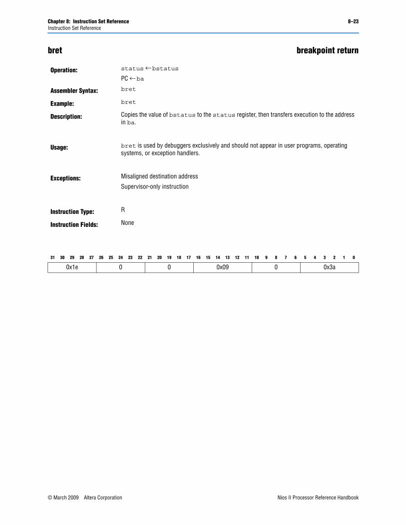
Chapter 8: Instruction Set Reference 8–23Instruction Set Reference
bret breakpoint return
Operation: status ← bstatus
PC ← ba
Assembler Syntax: bret
Example: bret
Description: Copies the value of bstatus to the status register, then transfers execution to the address in ba.
Usage: bret is used by debuggers exclusively and should not appear in user programs, operating systems, or exception handlers.
Exceptions: Misaligned destination address
Supervisor-only instruction
Instruction Type: R
Instruction Fields: None
31 30 29 28 27 26 25 24 23 22 21 20 19 18 17 16 15 14 13 12 11 10 9 8 7 6 5 4 3 2 1 0
0x1e 0 0 0x09 0 0x3a
© March 2009 Altera Corporation Nios II Processor Reference HandbookPreliminary
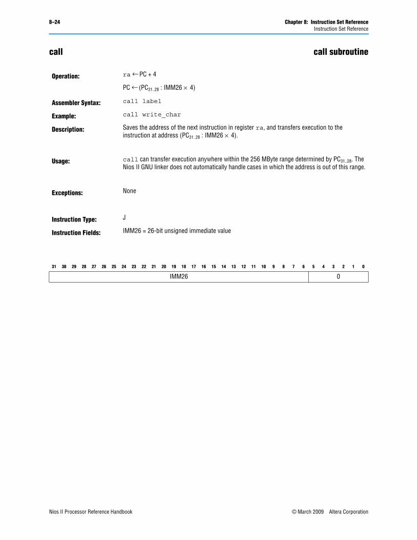
8–24 Chapter 8: Instruction Set ReferenceInstruction Set Reference
call call subroutine
Operation: ra ← PC + 4
PC ← (PC31..28 : IMM26 × 4)
Assembler Syntax: call label
Example: call write_char
Description: Saves the address of the next instruction in register ra, and transfers execution to the instruction at address (PC31..28 : IMM26 × 4).
Usage: call can transfer execution anywhere within the 256 MByte range determined by PC31..28. The Nios II GNU linker does not automatically handle cases in which the address is out of this range.
Exceptions: None
Instruction Type: J
Instruction Fields: IMM26 = 26-bit unsigned immediate value
31 30 29 28 27 26 25 24 23 22 21 20 19 18 17 16 15 14 13 12 11 10 9 8 7 6 5 4 3 2 1 0
IMM26 0
Nios II Processor Reference Handbook © March 2009 Altera CorporationPreliminary
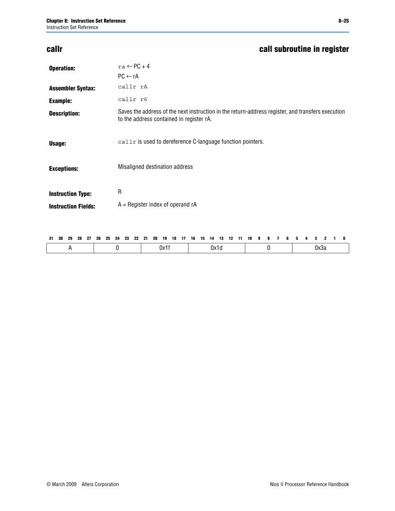
Chapter 8: Instruction Set Reference 8–25Instruction Set Reference
callr call subroutine in register
Operation: ra ← PC + 4
PC ← rA
Assembler Syntax: callr rA
Example: callr r6
Description: Saves the address of the next instruction in the return-address register, and transfers execution to the address contained in register rA.
Usage: callr is used to dereference C-language function pointers.
Exceptions: Misaligned destination address
Instruction Type: R
Instruction Fields: A = Register index of operand rA
31 30 29 28 27 26 25 24 23 22 21 20 19 18 17 16 15 14 13 12 11 10 9 8 7 6 5 4 3 2 1 0
A 0 0x1f 0x1d 0 0x3a
© March 2009 Altera Corporation Nios II Processor Reference HandbookPreliminary
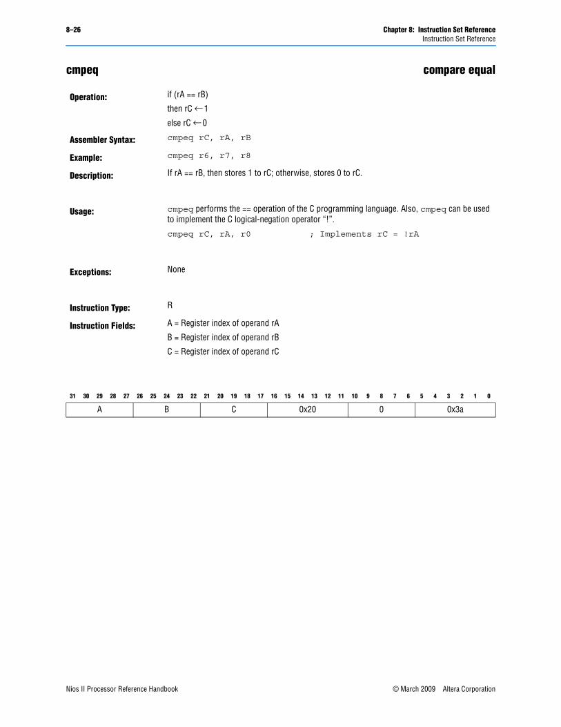
8–26 Chapter 8: Instruction Set ReferenceInstruction Set Reference
cmpeq compare equal
Operation: if (rA == rB)
then rC ← 1
else rC ← 0
Assembler Syntax: cmpeq rC, rA, rB
Example: cmpeq r6, r7, r8
Description: If rA == rB, then stores 1 to rC; otherwise, stores 0 to rC.
Usage: cmpeq performs the == operation of the C programming language. Also, cmpeq can be used to implement the C logical-negation operator “!”.
cmpeq rC, rA, r0 ; Implements rC = !rA
Exceptions: None
Instruction Type: R
Instruction Fields: A = Register index of operand rA
B = Register index of operand rB
C = Register index of operand rC
31 30 29 28 27 26 25 24 23 22 21 20 19 18 17 16 15 14 13 12 11 10 9 8 7 6 5 4 3 2 1 0
A B C 0x20 0 0x3a
Nios II Processor Reference Handbook © March 2009 Altera CorporationPreliminary
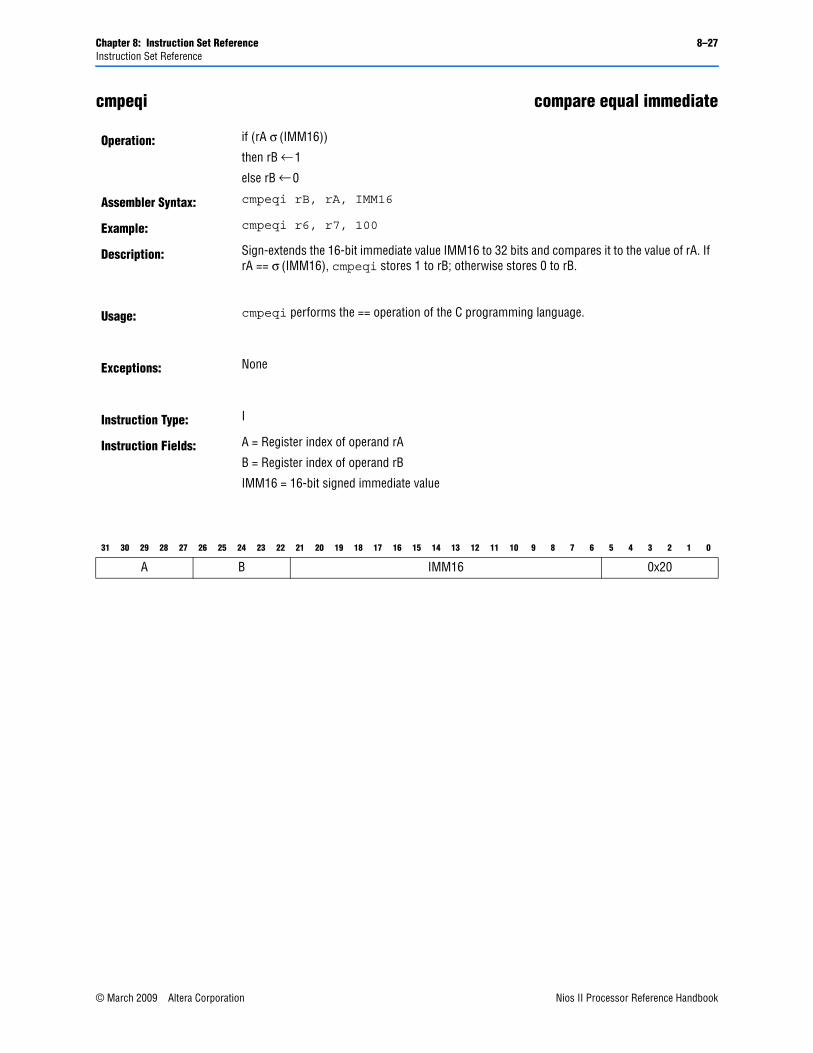
Chapter 8: Instruction Set Reference 8–27Instruction Set Reference
cmpeqi compare equal immediate
Operation: if (rA σ (IMM16))
then rB ← 1
else rB ← 0
Assembler Syntax: cmpeqi rB, rA, IMM16
Example: cmpeqi r6, r7, 100
Description: Sign-extends the 16-bit immediate value IMM16 to 32 bits and compares it to the value of rA. If rA == σ (IMM16), cmpeqi stores 1 to rB; otherwise stores 0 to rB.
Usage: cmpeqi performs the == operation of the C programming language.
Exceptions: None
Instruction Type: I
Instruction Fields: A = Register index of operand rA
B = Register index of operand rB
IMM16 = 16-bit signed immediate value
31 30 29 28 27 26 25 24 23 22 21 20 19 18 17 16 15 14 13 12 11 10 9 8 7 6 5 4 3 2 1 0
A B IMM16 0x20
© March 2009 Altera Corporation Nios II Processor Reference HandbookPreliminary
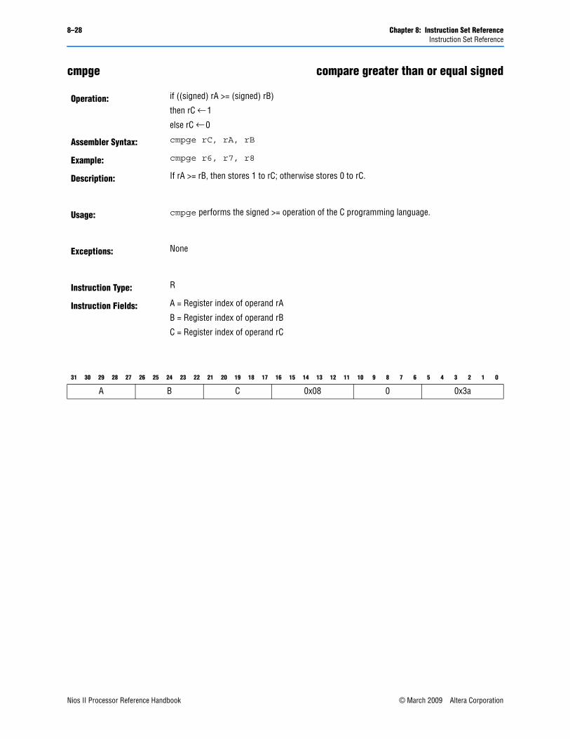
8–28 Chapter 8: Instruction Set ReferenceInstruction Set Reference
cmpge compare greater than or equal signed
Operation: if ((signed) rA >= (signed) rB)
then rC ← 1
else rC ← 0
Assembler Syntax: cmpge rC, rA, rB
Example: cmpge r6, r7, r8
Description: If rA >= rB, then stores 1 to rC; otherwise stores 0 to rC.
Usage: cmpge performs the signed >= operation of the C programming language.
Exceptions: None
Instruction Type: R
Instruction Fields: A = Register index of operand rA
B = Register index of operand rB
C = Register index of operand rC
31 30 29 28 27 26 25 24 23 22 21 20 19 18 17 16 15 14 13 12 11 10 9 8 7 6 5 4 3 2 1 0
A B C 0x08 0 0x3a
Nios II Processor Reference Handbook © March 2009 Altera CorporationPreliminary
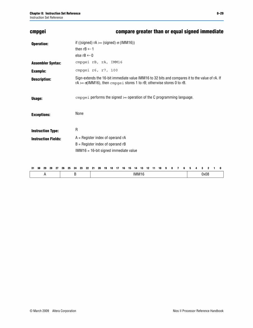
Chapter 8: Instruction Set Reference 8–29Instruction Set Reference
cmpgei compare greater than or equal signed immediate
Operation: if ((signed) rA >= (signed) σ (IMM16))
then rB ← 1
else rB ← 0
Assembler Syntax: cmpgei rB, rA, IMM16
Example: cmpgei r6, r7, 100
Description: Sign-extends the 16-bit immediate value IMM16 to 32 bits and compares it to the value of rA. If rA >= σ(IMM16), then cmpgei stores 1 to rB; otherwise stores 0 to rB.
Usage: cmpgei performs the signed >= operation of the C programming language.
Exceptions: None
Instruction Type: R
Instruction Fields: A = Register index of operand rA
B = Register index of operand rB
IMM16 = 16-bit signed immediate value
31 30 29 28 27 26 25 24 23 22 21 20 19 18 17 16 15 14 13 12 11 10 9 8 7 6 5 4 3 2 1 0
A B IMM16 0x08
© March 2009 Altera Corporation Nios II Processor Reference HandbookPreliminary
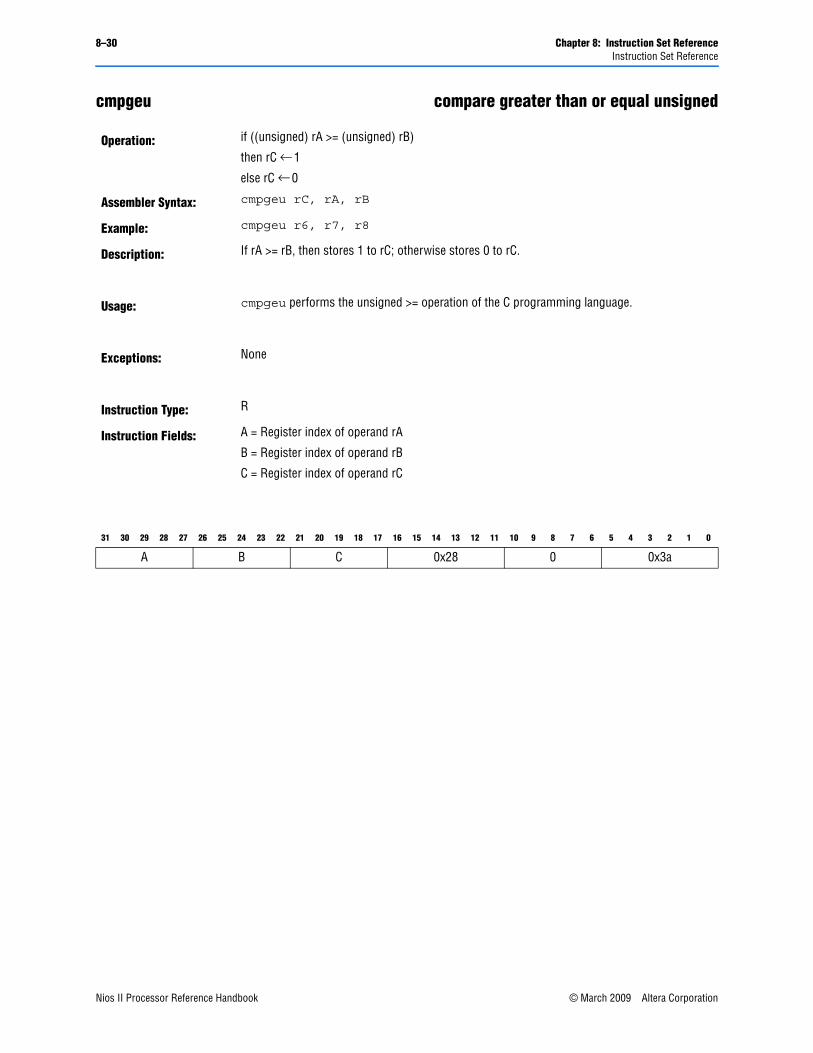
8–30 Chapter 8: Instruction Set ReferenceInstruction Set Reference
cmpgeu compare greater than or equal unsigned
Operation: if ((unsigned) rA >= (unsigned) rB)
then rC ← 1
else rC ← 0
Assembler Syntax: cmpgeu rC, rA, rB
Example: cmpgeu r6, r7, r8
Description: If rA >= rB, then stores 1 to rC; otherwise stores 0 to rC.
Usage: cmpgeu performs the unsigned >= operation of the C programming language.
Exceptions: None
Instruction Type: R
Instruction Fields: A = Register index of operand rA
B = Register index of operand rB
C = Register index of operand rC
31 30 29 28 27 26 25 24 23 22 21 20 19 18 17 16 15 14 13 12 11 10 9 8 7 6 5 4 3 2 1 0
A B C 0x28 0 0x3a
Nios II Processor Reference Handbook © March 2009 Altera CorporationPreliminary
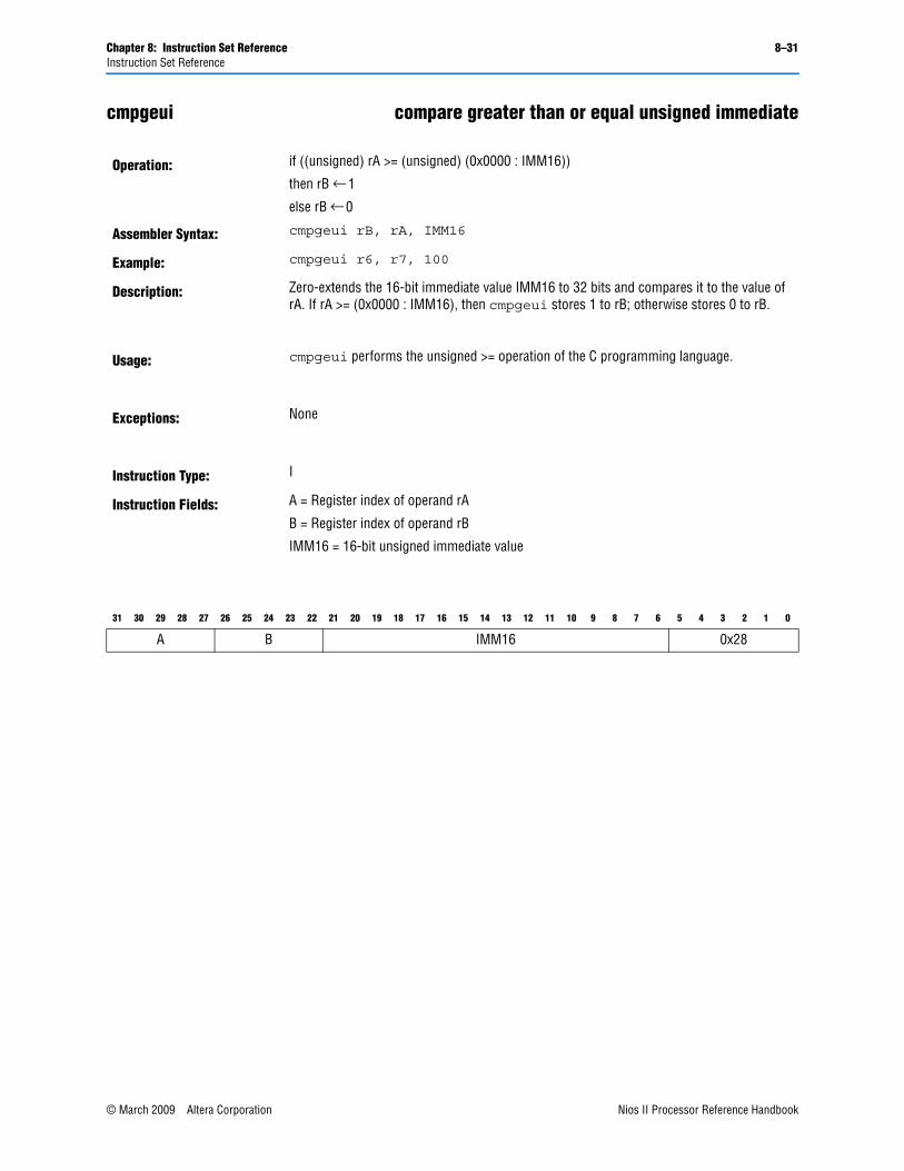
Chapter 8: Instruction Set Reference 8–31Instruction Set Reference
cmpgeui compare greater than or equal unsigned immediate
Operation: if ((unsigned) rA >= (unsigned) (0x0000 : IMM16))
then rB ← 1
else rB ← 0
Assembler Syntax: cmpgeui rB, rA, IMM16
Example: cmpgeui r6, r7, 100
Description: Zero-extends the 16-bit immediate value IMM16 to 32 bits and compares it to the value of rA. If rA >= (0x0000 : IMM16), then cmpgeui stores 1 to rB; otherwise stores 0 to rB.
Usage: cmpgeui performs the unsigned >= operation of the C programming language.
Exceptions: None
Instruction Type: I
Instruction Fields: A = Register index of operand rA
B = Register index of operand rB
IMM16 = 16-bit unsigned immediate value
31 30 29 28 27 26 25 24 23 22 21 20 19 18 17 16 15 14 13 12 11 10 9 8 7 6 5 4 3 2 1 0
A B IMM16 0x28
© March 2009 Altera Corporation Nios II Processor Reference HandbookPreliminary
8–32 Chapter 8: Instruction Set ReferenceInstruction Set Reference
cmpgt compare greater than signed
Operation: if ((signed) rA > (signed) rB)
then rC ← 1
else rC ← 0
Assembler Syntax: cmpgt rC, rA, rB
Example: cmpgt r6, r7, r8
Description: If rA > rB, then stores 1 to rC; otherwise stores 0 to rC.
Usage: cmpgt performs the signed > operation of the C programming language.
Pseudo-instruction: cmpgt is implemented with the cmplt instruction by swapping its rA and rB operands.
Nios II Processor Reference Handbook © March 2009 Altera CorporationPreliminary
Chapter 8: Instruction Set Reference 8–33Instruction Set Reference
cmpgti compare greater than signed immediate
Operation: if ((signed) rA > (signed) IMMED)
then rB ← 1
else rB ← 0
Assembler Syntax: cmpgti rB, rA, IMMED
Example: cmpgti r6, r7, 100
Description: Sign-extends the immediate value IMMED to 32 bits and compares it to the value of rA. If rA > σ(IMMED), then cmpgti stores 1 to rB; otherwise stores 0 to rB.
Usage: cmpgti performs the signed > operation of the C programming language. The maximum allowed value of IMMED is 32766. The minimum allowed value is –32769.
Pseudo-instruction: cmpgti is implemented using a cmpgei instruction with an IMM16 immediate value of IMMED + 1.
© March 2009 Altera Corporation Nios II Processor Reference HandbookPreliminary

8–34 Chapter 8: Instruction Set ReferenceInstruction Set Reference
cmpgtu compare greater than unsigned
Operation: if ((unsigned) rA > (unsigned) rB)
then rC ← 1
else rC ← 0
Assembler Syntax: cmpgtu rC, rA, rB
Example: cmpgtu r6, r7, r8
Description: If rA > rB, then stores 1 to rC; otherwise stores 0 to rC.
Usage: cmpgtu performs the unsigned > operation of the C programming language.
Pseudo-instruction: cmpgtu is implemented with the cmpltu instruction by swapping its rA and rB operands.
Nios II Processor Reference Handbook © March 2009 Altera CorporationPreliminary
Chapter 8: Instruction Set Reference 8–35Instruction Set Reference
cmpgtui compare greater than unsigned immediate
Operation: if ((unsigned) rA > (unsigned) IMMED)
then rB ← 1
else rB ← 0
Assembler Syntax: cmpgtui rB, rA, IMMED
Example: cmpgtui r6, r7, 100
Description: Zero-extends the immediate value IMMED to 32 bits and compares it to the value of rA. If rA > IMMED, then cmpgtui stores 1 to rB; otherwise stores 0 to rB.
Usage: cmpgtui performs the unsigned > operation of the C programming language. The maximum allowed value of IMMED is 65534. The minimum allowed value is 0.
Pseudo-instruction: cmpgtui is implemented using a cmpgeui instruction with an IMM16 immediate value of IMMED + 1.
© March 2009 Altera Corporation Nios II Processor Reference HandbookPreliminary
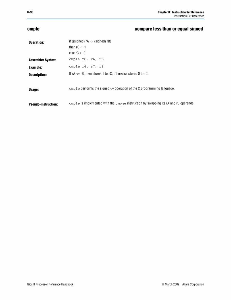
8–36 Chapter 8: Instruction Set ReferenceInstruction Set Reference
cmple compare less than or equal signed
Operation: if ((signed) rA <= (signed) rB)
then rC ← 1
else rC ← 0
Assembler Syntax: cmple rC, rA, rB
Example: cmple r6, r7, r8
Description: If rA <= rB, then stores 1 to rC; otherwise stores 0 to rC.
Usage: cmple performs the signed <= operation of the C programming language.
Pseudo-instruction: cmple is implemented with the cmpge instruction by swapping its rA and rB operands.
Nios II Processor Reference Handbook © March 2009 Altera CorporationPreliminary

Chapter 8: Instruction Set Reference 8–37Instruction Set Reference
cmplei compare less than or equal signed immediate
Operation: if ((signed) rA < (signed) IMMED)
then rB ← 1
else rB ← 0
Assembler Syntax: cmplei rB, rA, IMMED
Example: cmplei r6, r7, 100
Description: Sign-extends the immediate value IMMED to 32 bits and compares it to the value of rA. If rA <= σ(IMMED), then cmplei stores 1 to rB; otherwise stores 0 to rB.
Usage: cmplei performs the signed <= operation of the C programming language. The maximum allowed value of IMMED is 32766. The minimum allowed value is –32769.
Pseudo-instruction: cmplei is implemented using a cmplti instruction with an IMM16 immediate value of IMMED + 1.
© March 2009 Altera Corporation Nios II Processor Reference HandbookPreliminary
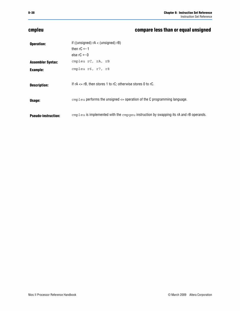
8–38 Chapter 8: Instruction Set ReferenceInstruction Set Reference
cmpleu compare less than or equal unsigned
Operation: if ((unsigned) rA < (unsigned) rB)
then rC ← 1
else rC ← 0
Assembler Syntax: cmpleu rC, rA, rB
Example: cmpleu r6, r7, r8
Description: If rA <= rB, then stores 1 to rC; otherwise stores 0 to rC.
Usage: cmpleu performs the unsigned <= operation of the C programming language.
Pseudo-instruction: cmpleu is implemented with the cmpgeu instruction by swapping its rA and rB operands.
Nios II Processor Reference Handbook © March 2009 Altera CorporationPreliminary

Chapter 8: Instruction Set Reference 8–39Instruction Set Reference
cmpleui compare less than or equal unsigned immediate
Operation: if ((unsigned) rA <= (unsigned) IMMED)
then rB ← 1
else rB ← 0
Assembler Syntax: cmpleui rB, rA, IMMED
Example: cmpleui r6, r7, 100
Description: Zero-extends the immediate value IMMED to 32 bits and compares it to the value of rA. If rA <= IMMED, then cmpleui stores 1 to rB; otherwise stores 0 to rB.
Usage: cmpleui performs the unsigned <= operation of the C programming language. The maximum allowed value of IMMED is 65534. The minimum allowed value is 0.
Pseudo-instruction: cmpleui is implemented using a cmpltui instruction with an IMM16 immediate value of IMMED + 1.
© March 2009 Altera Corporation Nios II Processor Reference HandbookPreliminary
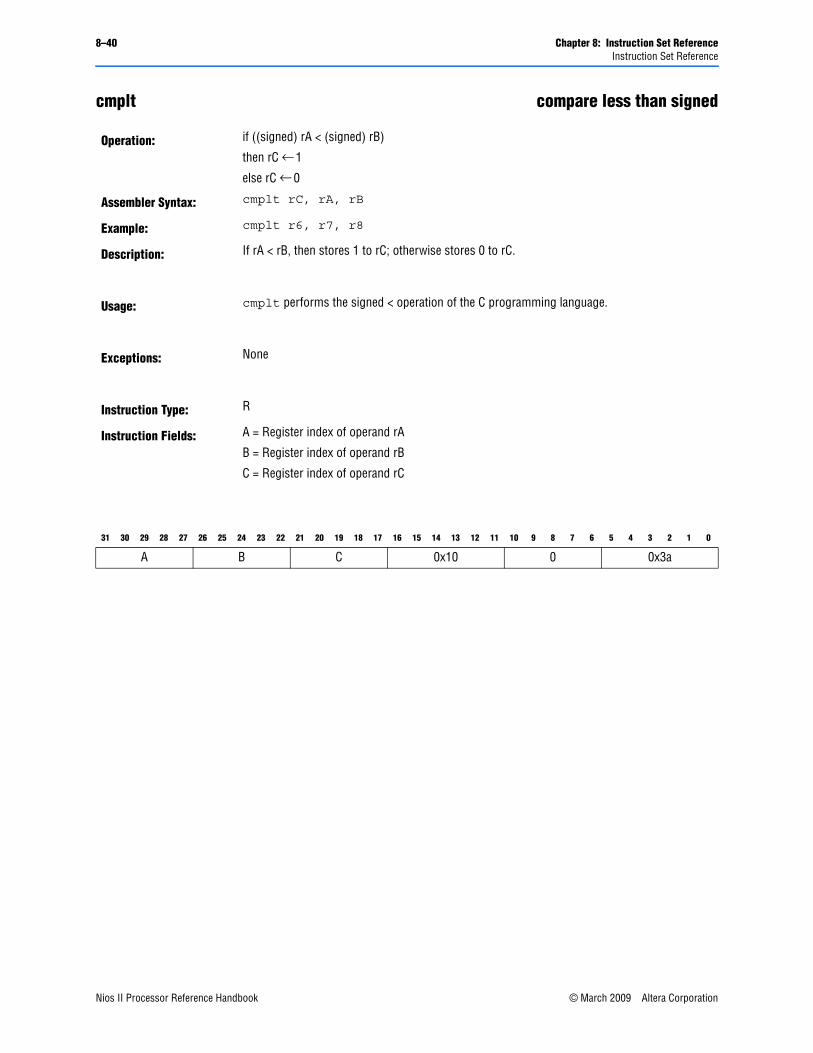
8–40 Chapter 8: Instruction Set ReferenceInstruction Set Reference
cmplt compare less than signed
Operation: if ((signed) rA < (signed) rB)
then rC ← 1
else rC ← 0
Assembler Syntax: cmplt rC, rA, rB
Example: cmplt r6, r7, r8
Description: If rA < rB, then stores 1 to rC; otherwise stores 0 to rC.
Usage: cmplt performs the signed < operation of the C programming language.
Exceptions: None
Instruction Type: R
Instruction Fields: A = Register index of operand rA
B = Register index of operand rB
C = Register index of operand rC
31 30 29 28 27 26 25 24 23 22 21 20 19 18 17 16 15 14 13 12 11 10 9 8 7 6 5 4 3 2 1 0
A B C 0x10 0 0x3a
Nios II Processor Reference Handbook © March 2009 Altera CorporationPreliminary
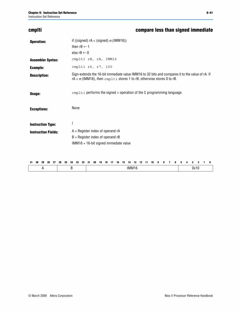
Chapter 8: Instruction Set Reference 8–41Instruction Set Reference
cmplti compare less than signed immediate
Operation: if ((signed) rA < (signed) σ (IMM16))
then rB ← 1
else rB ← 0
Assembler Syntax: cmplti rB, rA, IMM16
Example: cmplti r6, r7, 100
Description: Sign-extends the 16-bit immediate value IMM16 to 32 bits and compares it to the value of rA. If rA < σ (IMM16), then cmplti stores 1 to rB; otherwise stores 0 to rB.
Usage: cmplti performs the signed < operation of the C programming language.
Exceptions: None
Instruction Type: I
Instruction Fields: A = Register index of operand rA
B = Register index of operand rB
IMM16 = 16-bit signed immediate value
31 30 29 28 27 26 25 24 23 22 21 20 19 18 17 16 15 14 13 12 11 10 9 8 7 6 5 4 3 2 1 0
A B IMM16 0x10
© March 2009 Altera Corporation Nios II Processor Reference HandbookPreliminary
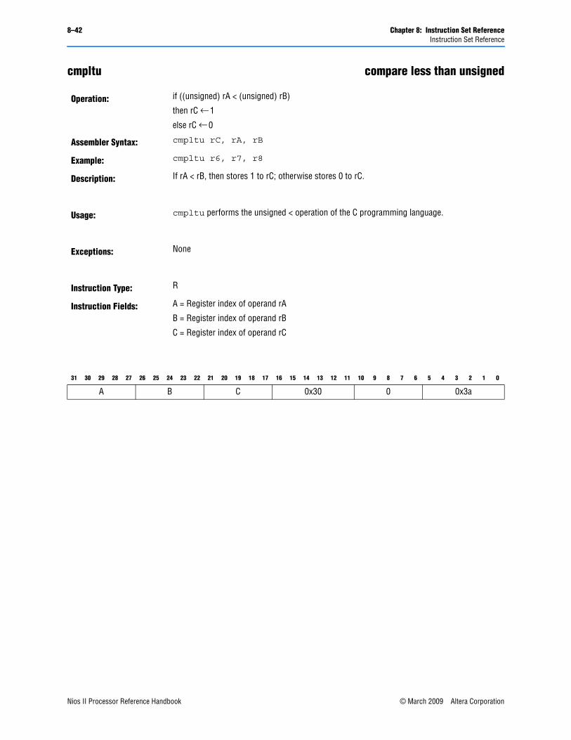
8–42 Chapter 8: Instruction Set ReferenceInstruction Set Reference
cmpltu compare less than unsigned
Operation: if ((unsigned) rA < (unsigned) rB)
then rC ← 1
else rC ← 0
Assembler Syntax: cmpltu rC, rA, rB
Example: cmpltu r6, r7, r8
Description: If rA < rB, then stores 1 to rC; otherwise stores 0 to rC.
Usage: cmpltu performs the unsigned < operation of the C programming language.
Exceptions: None
Instruction Type: R
Instruction Fields: A = Register index of operand rA
B = Register index of operand rB
C = Register index of operand rC
31 30 29 28 27 26 25 24 23 22 21 20 19 18 17 16 15 14 13 12 11 10 9 8 7 6 5 4 3 2 1 0
A B C 0x30 0 0x3a
Nios II Processor Reference Handbook © March 2009 Altera CorporationPreliminary
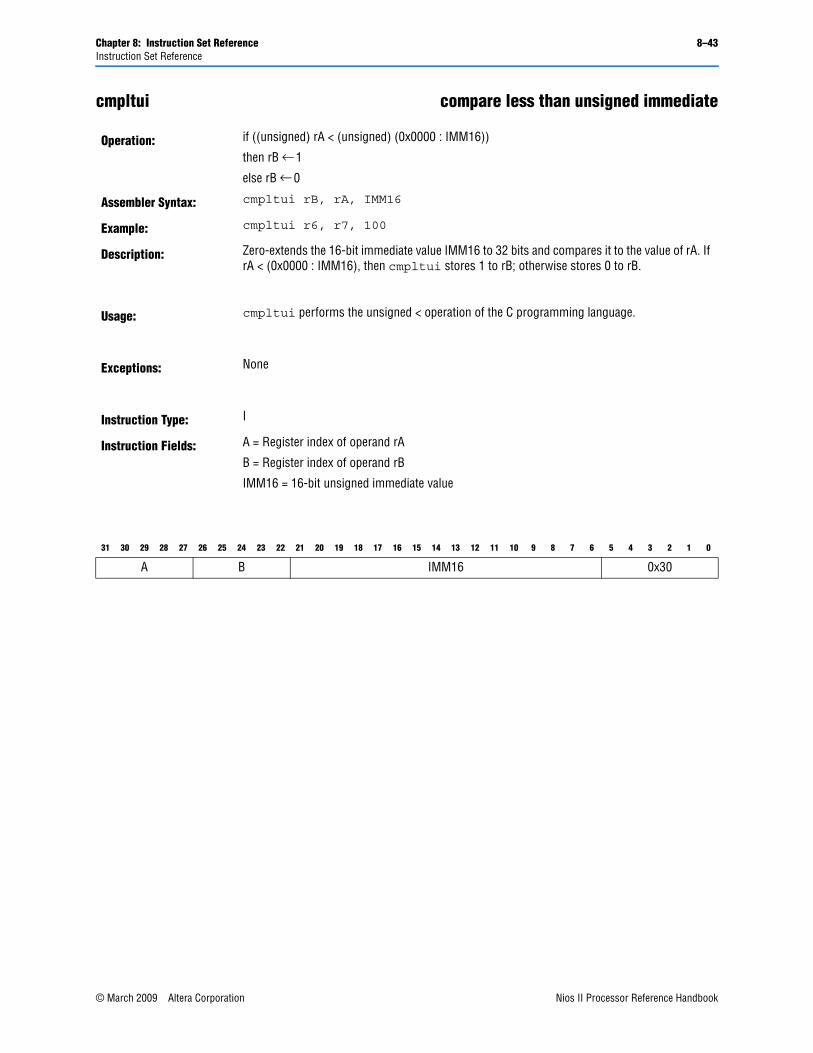
Chapter 8: Instruction Set Reference 8–43Instruction Set Reference
cmpltui compare less than unsigned immediate
Operation: if ((unsigned) rA < (unsigned) (0x0000 : IMM16))
then rB ← 1
else rB ← 0
Assembler Syntax: cmpltui rB, rA, IMM16
Example: cmpltui r6, r7, 100
Description: Zero-extends the 16-bit immediate value IMM16 to 32 bits and compares it to the value of rA. If rA < (0x0000 : IMM16), then cmpltui stores 1 to rB; otherwise stores 0 to rB.
Usage: cmpltui performs the unsigned < operation of the C programming language.
Exceptions: None
Instruction Type: I
Instruction Fields: A = Register index of operand rA
B = Register index of operand rB
IMM16 = 16-bit unsigned immediate value
31 30 29 28 27 26 25 24 23 22 21 20 19 18 17 16 15 14 13 12 11 10 9 8 7 6 5 4 3 2 1 0
A B IMM16 0x30
© March 2009 Altera Corporation Nios II Processor Reference HandbookPreliminary
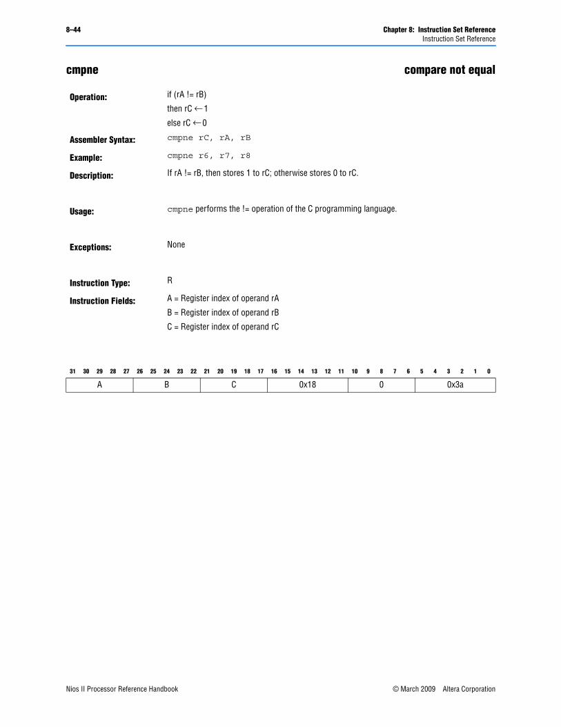
8–44 Chapter 8: Instruction Set ReferenceInstruction Set Reference
cmpne compare not equal
Operation: if (rA != rB)
then rC ← 1
else rC ← 0
Assembler Syntax: cmpne rC, rA, rB
Example: cmpne r6, r7, r8
Description: If rA != rB, then stores 1 to rC; otherwise stores 0 to rC.
Usage: cmpne performs the != operation of the C programming language.
Exceptions: None
Instruction Type: R
Instruction Fields: A = Register index of operand rA
B = Register index of operand rB
C = Register index of operand rC
31 30 29 28 27 26 25 24 23 22 21 20 19 18 17 16 15 14 13 12 11 10 9 8 7 6 5 4 3 2 1 0
A B C 0x18 0 0x3a
Nios II Processor Reference Handbook © March 2009 Altera CorporationPreliminary
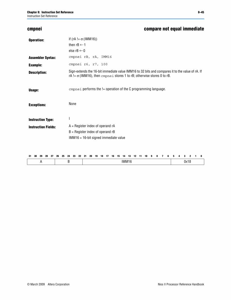
Chapter 8: Instruction Set Reference 8–45Instruction Set Reference
cmpnei compare not equal immediate
Operation: if (rA != σ (IMM16))
then rB ← 1
else rB ← 0
Assembler Syntax: cmpnei rB, rA, IMM16
Example: cmpnei r6, r7, 100
Description: Sign-extends the 16-bit immediate value IMM16 to 32 bits and compares it to the value of rA. If rA != σ (IMM16), then cmpnei stores 1 to rB; otherwise stores 0 to rB.
Usage: cmpnei performs the != operation of the C programming language.
Exceptions: None
Instruction Type: I
Instruction Fields: A = Register index of operand rA
B = Register index of operand rB
IMM16 = 16-bit signed immediate value
31 30 29 28 27 26 25 24 23 22 21 20 19 18 17 16 15 14 13 12 11 10 9 8 7 6 5 4 3 2 1 0
A B IMM16 0x18
© March 2009 Altera Corporation Nios II Processor Reference HandbookPreliminary
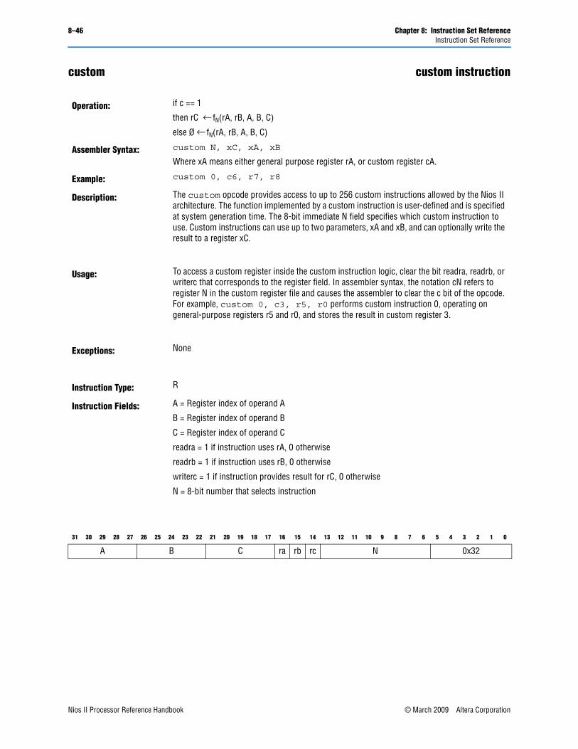
8–46 Chapter 8: Instruction Set ReferenceInstruction Set Reference
custom custom instruction
Operation: if c == 1
then rC ← fN(rA, rB, A, B, C)
else Ø ← fN(rA, rB, A, B, C)
Assembler Syntax: custom N, xC, xA, xB
Where xA means either general purpose register rA, or custom register cA.
Example: custom 0, c6, r7, r8
Description: The custom opcode provides access to up to 256 custom instructions allowed by the Nios II architecture. The function implemented by a custom instruction is user-defined and is specified at system generation time. The 8-bit immediate N field specifies which custom instruction to use. Custom instructions can use up to two parameters, xA and xB, and can optionally write the result to a register xC.
Usage: To access a custom register inside the custom instruction logic, clear the bit readra, readrb, or writerc that corresponds to the register field. In assembler syntax, the notation cN refers to register N in the custom register file and causes the assembler to clear the c bit of the opcode. For example, custom 0, c3, r5, r0 performs custom instruction 0, operating on general-purpose registers r5 and r0, and stores the result in custom register 3.
Exceptions: None
Instruction Type: R
Instruction Fields: A = Register index of operand A
B = Register index of operand B
C = Register index of operand C
readra = 1 if instruction uses rA, 0 otherwise
readrb = 1 if instruction uses rB, 0 otherwise
writerc = 1 if instruction provides result for rC, 0 otherwise
N = 8-bit number that selects instruction
31 30 29 28 27 26 25 24 23 22 21 20 19 18 17 16 15 14 13 12 11 10 9 8 7 6 5 4 3 2 1 0
A B C ra rb rc N 0x32
Nios II Processor Reference Handbook © March 2009 Altera CorporationPreliminary
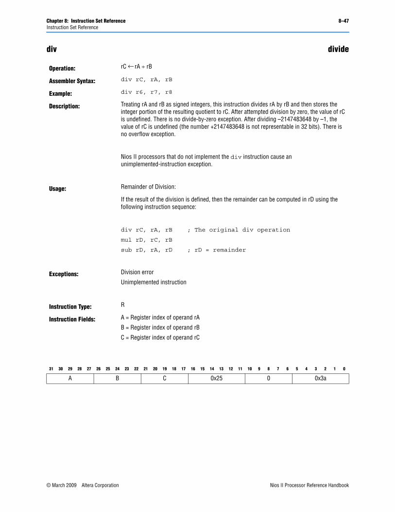
Chapter 8: Instruction Set Reference 8–47Instruction Set Reference
div divide
Operation: rC ← rA ÷ rB
Assembler Syntax: div rC, rA, rB
Example: div r6, r7, r8
Description: Treating rA and rB as signed integers, this instruction divides rA by rB and then stores the integer portion of the resulting quotient to rC. After attempted division by zero, the value of rC is undefined. There is no divide-by-zero exception. After dividing –2147483648 by –1, the value of rC is undefined (the number +2147483648 is not representable in 32 bits). There is no overflow exception.
Nios II processors that do not implement the div instruction cause an unimplemented-instruction exception.
Usage: Remainder of Division:
If the result of the division is defined, then the remainder can be computed in rD using the following instruction sequence:
div rC, rA, rB
mul rD, rC, rB
sub rD, rA, rD
; The original div operation
; rD = remainder
Exceptions: Division error
Unimplemented instruction
Instruction Type: R
Instruction Fields: A = Register index of operand rA
B = Register index of operand rB
C = Register index of operand rC
31 30 29 28 27 26 25 24 23 22 21 20 19 18 17 16 15 14 13 12 11 10 9 8 7 6 5 4 3 2 1 0
A B C 0x25 0 0x3a
© March 2009 Altera Corporation Nios II Processor Reference HandbookPreliminary
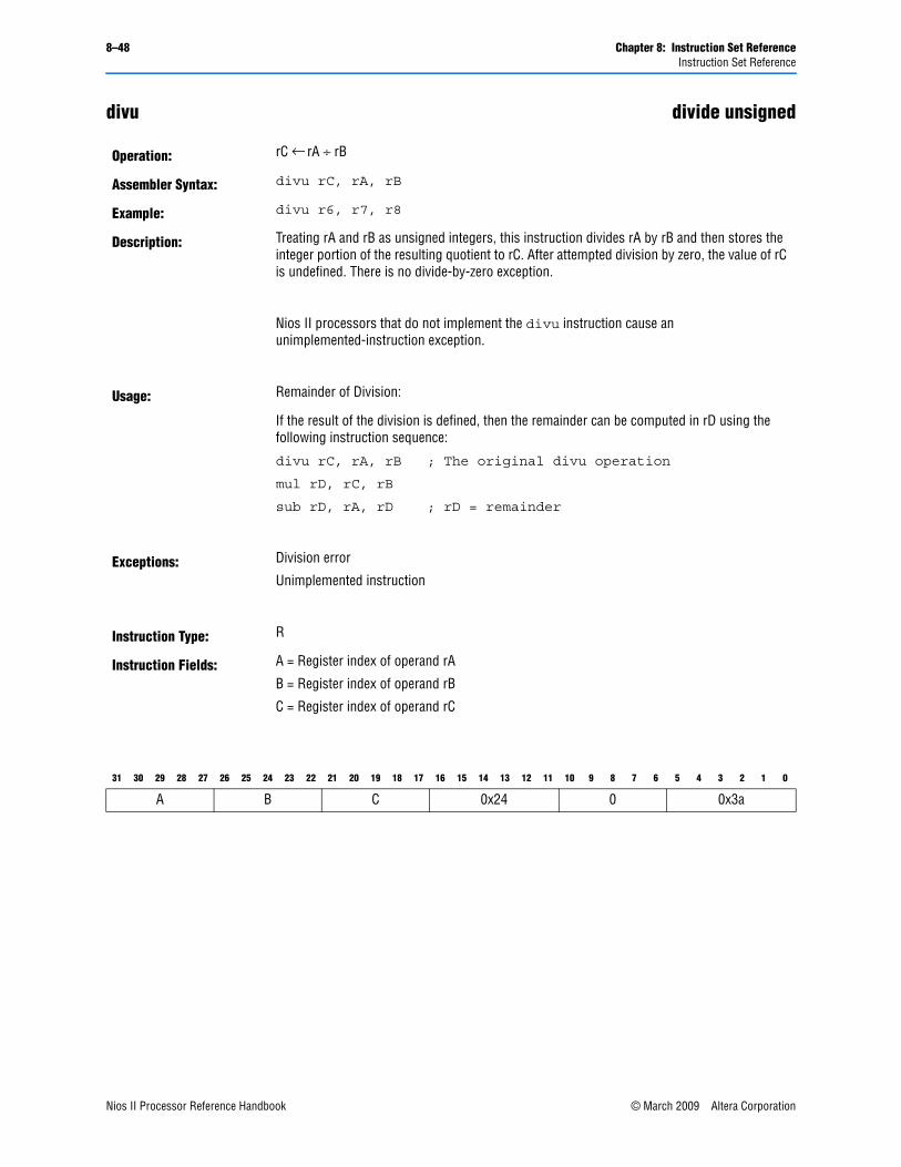
8–48 Chapter 8: Instruction Set ReferenceInstruction Set Reference
divu divide unsigned
Operation: rC ← rA ÷ rB
Assembler Syntax: divu rC, rA, rB
Example: divu r6, r7, r8
Description: Treating rA and rB as unsigned integers, this instruction divides rA by rB and then stores the integer portion of the resulting quotient to rC. After attempted division by zero, the value of rC is undefined. There is no divide-by-zero exception.
Nios II processors that do not implement the divu instruction cause an unimplemented-instruction exception.
Usage: Remainder of Division:
If the result of the division is defined, then the remainder can be computed in rD using the following instruction sequence:
divu rC, rA, rB
mul rD, rC, rB
sub rD, rA, rD
; The original divu operation
; rD = remainder
Exceptions: Division error
Unimplemented instruction
Instruction Type: R
Instruction Fields: A = Register index of operand rA
B = Register index of operand rB
C = Register index of operand rC
31 30 29 28 27 26 25 24 23 22 21 20 19 18 17 16 15 14 13 12 11 10 9 8 7 6 5 4 3 2 1 0
A B C 0x24 0 0x3a
Nios II Processor Reference Handbook © March 2009 Altera CorporationPreliminary
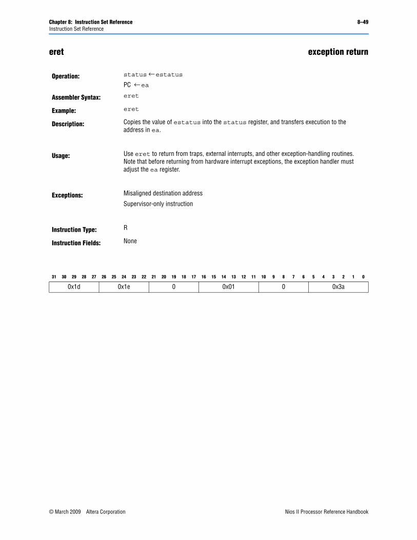
Chapter 8: Instruction Set Reference 8–49Instruction Set Reference
eret exception return
Operation: status ← estatus
PC ← ea
Assembler Syntax: eret
Example: eret
Description: Copies the value of estatus into the status register, and transfers execution to the address in ea.
Usage: Use eret to return from traps, external interrupts, and other exception-handling routines. Note that before returning from hardware interrupt exceptions, the exception handler must adjust the ea register.
Exceptions: Misaligned destination address
Supervisor-only instruction
Instruction Type: R
Instruction Fields: None
31 30 29 28 27 26 25 24 23 22 21 20 19 18 17 16 15 14 13 12 11 10 9 8 7 6 5 4 3 2 1 0
0x1d 0x1e 0 0x01 0 0x3a
© March 2009 Altera Corporation Nios II Processor Reference HandbookPreliminary
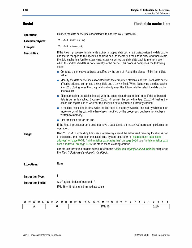
8–50 Chapter 8: Instruction Set ReferenceInstruction Set Reference
flushd flush data cache line
Operation: Flushes the data cache line associated with address rA + σ (IMM16).
Assembler Syntax: flushd IMM16(rA)
Example: flushd -100(r6)
Description: If the Nios II processor implements a direct mapped data cache, flushd writes the data cache line that is mapped to the specified address back to memory if the line is dirty, and then clears the data cache line. Unlike flushda, flushd writes the dirty data back to memory even when the addressed data is not currently in the cache. This process comprises the following steps:
■ Compute the effective address specified by the sum of rA and the signed 16-bit immediate value.
■ Identify the data cache line associated with the computed effective address. Each data cache effective address comprises a tag field and a line field. When identifying the data cache line, flushd ignores the tag field and only uses the line field to select the data cache line to clear.
■ Skip comparing the cache line tag with the effective address to determine if the addressed data is currently cached. Because flushd ignores the cache line tag, flushd flushes the cache line regardless of whether the specified data location is currently cached.
■ If the data cache line is dirty, write the line back to memory. A cache line is dirty when one or more words of the cache line have been modified by the processor, but have not yet been written to memory.
■ Clear the valid bit for the line.
If the Nios II processor core does not have a data cache, the flushd instruction performs no operation.
Usage: Use flushd to write dirty lines back to memory even if the addressed memory location is not in the cache, and then flush the cache line. By contrast, refer to “flushda flush data cache address” on page 8–51, “initd initialize data cache line” on page 8–54, and “initda initialize data cache address” on page 8–55 for other cache-clearing options.
For more information on data cache, refer to the Cache and Tightly Coupled Memory chapter of the Nios II Software Developer’s Handbook.
Exceptions: None
Instruction Type: I
Instruction Fields: A = Register index of operand rA
IMM16 = 16-bit signed immediate value
31 30 29 28 27 26 25 24 23 22 21 20 19 18 17 16 15 14 13 12 11 10 9 8 7 6 5 4 3 2 1 0
A 0 IMM16 0x3b
Nios II Processor Reference Handbook © March 2009 Altera CorporationPreliminary
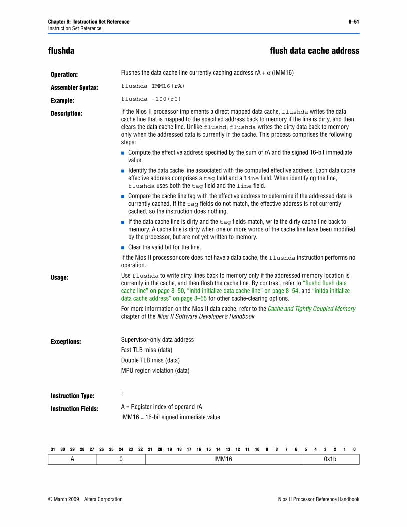
Chapter 8: Instruction Set Reference 8–51Instruction Set Reference
flushda flush data cache address
Operation: Flushes the data cache line currently caching address rA + σ (IMM16)
Assembler Syntax: flushda IMM16(rA)
Example: flushda -100(r6)
Description: If the Nios II processor implements a direct mapped data cache, flushda writes the data cache line that is mapped to the specified address back to memory if the line is dirty, and then clears the data cache line. Unlike flushd, flushda writes the dirty data back to memory only when the addressed data is currently in the cache. This process comprises the following steps:
■ Compute the effective address specified by the sum of rA and the signed 16-bit immediate value.
■ Identify the data cache line associated with the computed effective address. Each data cache effective address comprises a tag field and a line field. When identifying the line, flushda uses both the tag field and the line field.
■ Compare the cache line tag with the effective address to determine if the addressed data is currently cached. If the tag fields do not match, the effective address is not currently cached, so the instruction does nothing.
■ If the data cache line is dirty and the tag fields match, write the dirty cache line back to memory. A cache line is dirty when one or more words of the cache line have been modified by the processor, but are not yet written to memory.
■ Clear the valid bit for the line.
If the Nios II processor core does not have a data cache, the flushda instruction performs no operation.
Usage: Use flushda to write dirty lines back to memory only if the addressed memory location is currently in the cache, and then flush the cache line. By contrast, refer to “flushd flush data cache line” on page 8–50, “initd initialize data cache line” on page 8–54, and “initda initialize data cache address” on page 8–55 for other cache-clearing options.
For more information on the Nios II data cache, refer to the Cache and Tightly Coupled Memory chapter of the Nios II Software Developer’s Handbook.
Exceptions: Supervisor-only data address
Fast TLB miss (data)
Double TLB miss (data)
MPU region violation (data)
Instruction Type: I
Instruction Fields: A = Register index of operand rA
IMM16 = 16-bit signed immediate value
31 30 29 28 27 26 25 24 23 22 21 20 19 18 17 16 15 14 13 12 11 10 9 8 7 6 5 4 3 2 1 0
A 0 IMM16 0x1b
© March 2009 Altera Corporation Nios II Processor Reference HandbookPreliminary
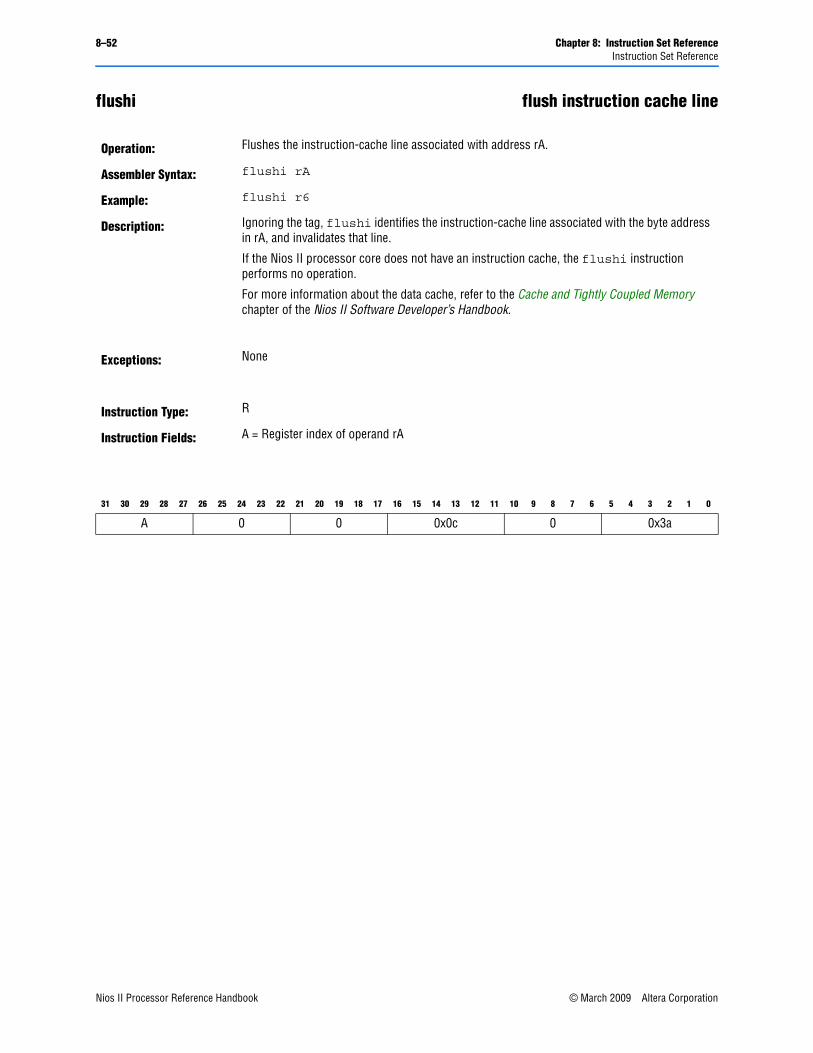
8–52 Chapter 8: Instruction Set ReferenceInstruction Set Reference
flushi flush instruction cache line
Operation: Flushes the instruction-cache line associated with address rA.
Assembler Syntax: flushi rA
Example: flushi r6
Description: Ignoring the tag, flushi identifies the instruction-cache line associated with the byte address in rA, and invalidates that line.
If the Nios II processor core does not have an instruction cache, the flushi instruction performs no operation.
For more information about the data cache, refer to the Cache and Tightly Coupled Memory chapter of the Nios II Software Developer’s Handbook.
Exceptions: None
Instruction Type: R
Instruction Fields: A = Register index of operand rA
31 30 29 28 27 26 25 24 23 22 21 20 19 18 17 16 15 14 13 12 11 10 9 8 7 6 5 4 3 2 1 0
A 0 0 0x0c 0 0x3a
Nios II Processor Reference Handbook © March 2009 Altera CorporationPreliminary
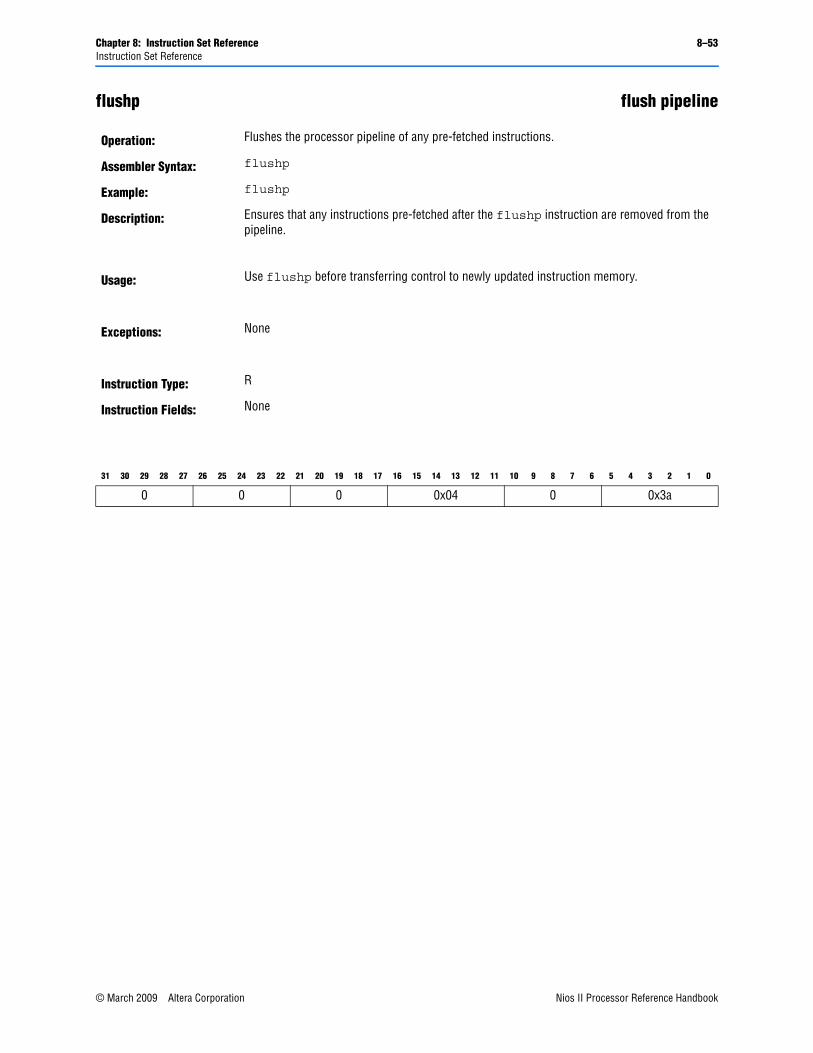
Chapter 8: Instruction Set Reference 8–53Instruction Set Reference
flushp flush pipeline
Operation: Flushes the processor pipeline of any pre-fetched instructions.
Assembler Syntax: flushp
Example: flushp
Description: Ensures that any instructions pre-fetched after the flushp instruction are removed from the pipeline.
Usage: Use flushp before transferring control to newly updated instruction memory.
Exceptions: None
Instruction Type: R
Instruction Fields: None
31 30 29 28 27 26 25 24 23 22 21 20 19 18 17 16 15 14 13 12 11 10 9 8 7 6 5 4 3 2 1 0
0 0 0 0x04 0 0x3a
© March 2009 Altera Corporation Nios II Processor Reference HandbookPreliminary
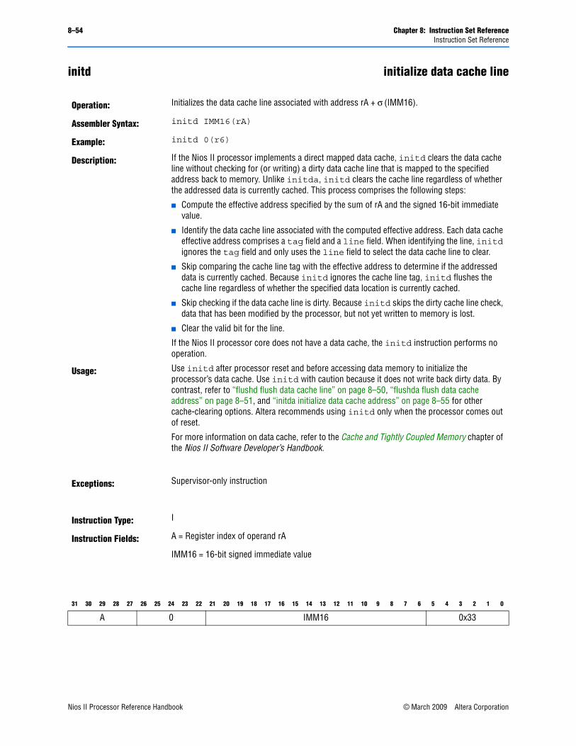
8–54 Chapter 8: Instruction Set ReferenceInstruction Set Reference
initd initialize data cache line
Operation: Initializes the data cache line associated with address rA + σ (IMM16).
Assembler Syntax: initd IMM16(rA)
Example: initd 0(r6)
Description: If the Nios II processor implements a direct mapped data cache, initd clears the data cache line without checking for (or writing) a dirty data cache line that is mapped to the specified address back to memory. Unlike initda, initd clears the cache line regardless of whether the addressed data is currently cached. This process comprises the following steps:
■ Compute the effective address specified by the sum of rA and the signed 16-bit immediate value.
■ Identify the data cache line associated with the computed effective address. Each data cache effective address comprises a tag field and a line field. When identifying the line, initd ignores the tag field and only uses the line field to select the data cache line to clear.
■ Skip comparing the cache line tag with the effective address to determine if the addressed data is currently cached. Because initd ignores the cache line tag, initd flushes the cache line regardless of whether the specified data location is currently cached.
■ Skip checking if the data cache line is dirty. Because initd skips the dirty cache line check, data that has been modified by the processor, but not yet written to memory is lost.
■ Clear the valid bit for the line.
If the Nios II processor core does not have a data cache, the initd instruction performs no operation.
Usage: Use initd after processor reset and before accessing data memory to initialize the processor’s data cache. Use initd with caution because it does not write back dirty data. By contrast, refer to “flushd flush data cache line” on page 8–50, “flushda flush data cache address” on page 8–51, and “initda initialize data cache address” on page 8–55 for other cache-clearing options. Altera recommends using initd only when the processor comes out of reset.
For more information on data cache, refer to the Cache and Tightly Coupled Memory chapter of the Nios II Software Developer’s Handbook.
Exceptions: Supervisor-only instruction
Instruction Type: I
Instruction Fields: A = Register index of operand rA
IMM16 = 16-bit signed immediate value
31 30 29 28 27 26 25 24 23 22 21 20 19 18 17 16 15 14 13 12 11 10 9 8 7 6 5 4 3 2 1 0
A 0 IMM16 0x33
Nios II Processor Reference Handbook © March 2009 Altera CorporationPreliminary
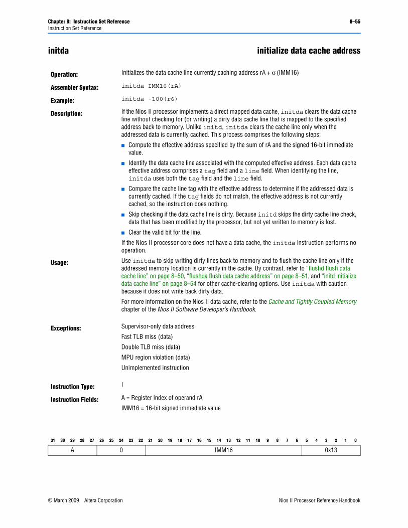
Chapter 8: Instruction Set Reference 8–55Instruction Set Reference
initda initialize data cache address
Operation: Initializes the data cache line currently caching address rA + σ (IMM16)
Assembler Syntax: initda IMM16(rA)
Example: initda -100(r6)
Description: If the Nios II processor implements a direct mapped data cache, initda clears the data cache line without checking for (or writing) a dirty data cache line that is mapped to the specified address back to memory. Unlike initd, initda clears the cache line only when the addressed data is currently cached. This process comprises the following steps:
■ Compute the effective address specified by the sum of rA and the signed 16-bit immediate value.
■ Identify the data cache line associated with the computed effective address. Each data cache effective address comprises a tag field and a line field. When identifying the line, initda uses both the tag field and the line field.
■ Compare the cache line tag with the effective address to determine if the addressed data is currently cached. If the tag fields do not match, the effective address is not currently cached, so the instruction does nothing.
■ Skip checking if the data cache line is dirty. Because initd skips the dirty cache line check, data that has been modified by the processor, but not yet written to memory is lost.
■ Clear the valid bit for the line.
If the Nios II processor core does not have a data cache, the initda instruction performs no operation.
Usage: Use initda to skip writing dirty lines back to memory and to flush the cache line only if the addressed memory location is currently in the cache. By contrast, refer to “flushd flush data cache line” on page 8–50, “flushda flush data cache address” on page 8–51, and “initd initialize data cache line” on page 8–54 for other cache-clearing options. Use initda with caution because it does not write back dirty data.
For more information on the Nios II data cache, refer to the Cache and Tightly Coupled Memory chapter of the Nios II Software Developer’s Handbook.
Exceptions: Supervisor-only data address
Fast TLB miss (data)
Double TLB miss (data)
MPU region violation (data)
Unimplemented instruction
Instruction Type: I
Instruction Fields: A = Register index of operand rA
IMM16 = 16-bit signed immediate value
31 30 29 28 27 26 25 24 23 22 21 20 19 18 17 16 15 14 13 12 11 10 9 8 7 6 5 4 3 2 1 0
A 0 IMM16 0x13
© March 2009 Altera Corporation Nios II Processor Reference HandbookPreliminary
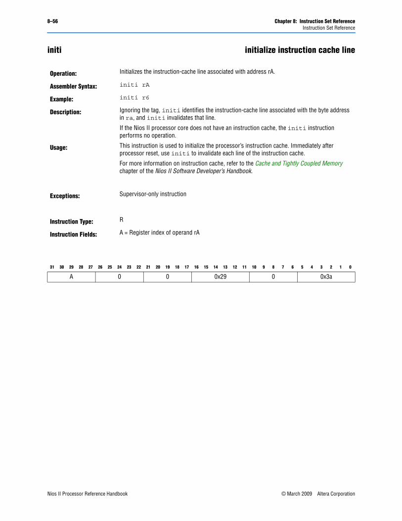
8–56 Chapter 8: Instruction Set ReferenceInstruction Set Reference
initi initialize instruction cache line
Operation: Initializes the instruction-cache line associated with address rA.
Assembler Syntax: initi rA
Example: initi r6
Description: Ignoring the tag, initi identifies the instruction-cache line associated with the byte address in ra, and initi invalidates that line.
If the Nios II processor core does not have an instruction cache, the initi instruction performs no operation.
Usage: This instruction is used to initialize the processor’s instruction cache. Immediately after processor reset, use initi to invalidate each line of the instruction cache.
For more information on instruction cache, refer to the Cache and Tightly Coupled Memory chapter of the Nios II Software Developer’s Handbook.
Exceptions: Supervisor-only instruction
Instruction Type: R
Instruction Fields: A = Register index of operand rA
31 30 29 28 27 26 25 24 23 22 21 20 19 18 17 16 15 14 13 12 11 10 9 8 7 6 5 4 3 2 1 0
A 0 0 0x29 0 0x3a
Nios II Processor Reference Handbook © March 2009 Altera CorporationPreliminary
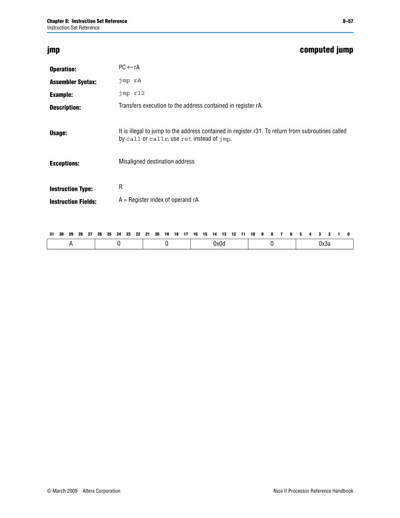
Chapter 8: Instruction Set Reference 8–57Instruction Set Reference
jmp computed jump
Operation: PC ← rA
Assembler Syntax: jmp rA
Example: jmp r12
Description: Transfers execution to the address contained in register rA.
Usage: It is illegal to jump to the address contained in register r31. To return from subroutines called by call or callr, use ret instead of jmp.
Exceptions: Misaligned destination address
Instruction Type: R
Instruction Fields: A = Register index of operand rA
31 30 29 28 27 26 25 24 23 22 21 20 19 18 17 16 15 14 13 12 11 10 9 8 7 6 5 4 3 2 1 0
A 0 0 0x0d 0 0x3a
© March 2009 Altera Corporation Nios II Processor Reference HandbookPreliminary
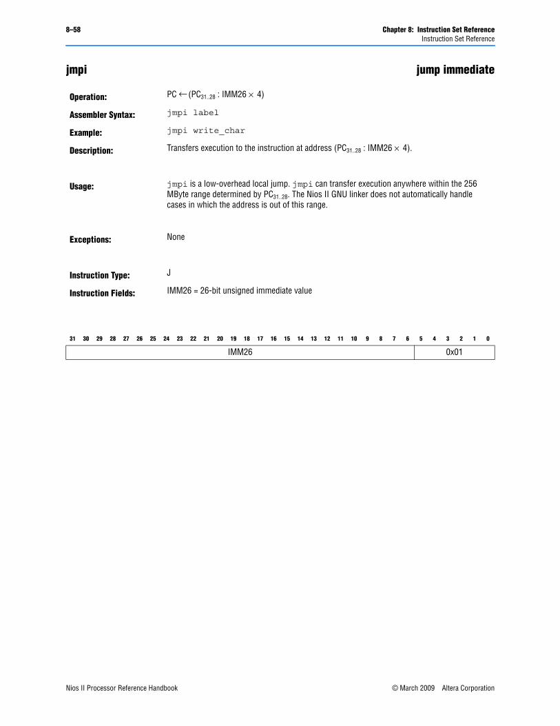
8–58 Chapter 8: Instruction Set ReferenceInstruction Set Reference
jmpi jump immediate
Operation: PC ← (PC31..28 : IMM26 × 4)
Assembler Syntax: jmpi label
Example: jmpi write_char
Description: Transfers execution to the instruction at address (PC31..28 : IMM26 × 4).
Usage: jmpi is a low-overhead local jump. jmpi can transfer execution anywhere within the 256 MByte range determined by PC31..28. The Nios II GNU linker does not automatically handle cases in which the address is out of this range.
Exceptions: None
Instruction Type: J
Instruction Fields: IMM26 = 26-bit unsigned immediate value
31 30 29 28 27 26 25 24 23 22 21 20 19 18 17 16 15 14 13 12 11 10 9 8 7 6 5 4 3 2 1 0
IMM26 0x01
Nios II Processor Reference Handbook © March 2009 Altera CorporationPreliminary
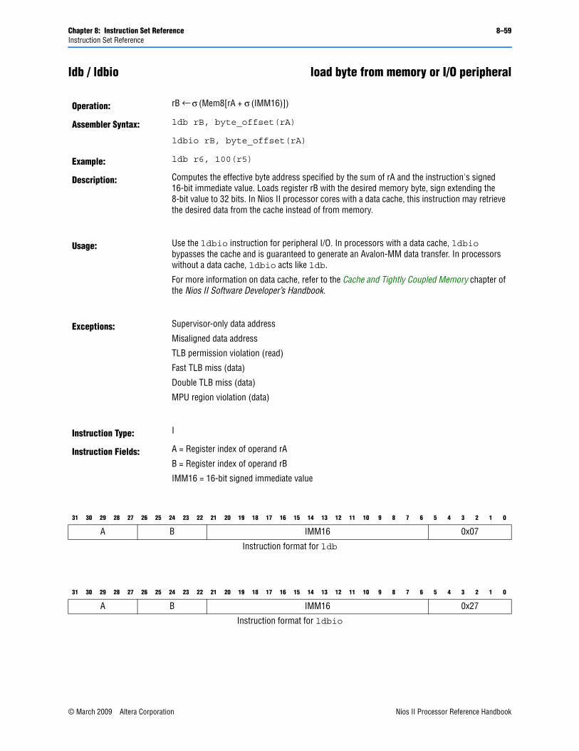
Chapter 8: Instruction Set Reference 8–59Instruction Set Reference
ldb / ldbio load byte from memory or I/O peripheral
Operation: rB ← σ (Mem8[rA + σ (IMM16)])
Assembler Syntax: ldb rB, byte_offset(rA)
ldbio rB, byte_offset(rA)
Example: ldb r6, 100(r5)
Description: Computes the effective byte address specified by the sum of rA and the instruction's signed 16-bit immediate value. Loads register rB with the desired memory byte, sign extending the 8-bit value to 32 bits. In Nios II processor cores with a data cache, this instruction may retrieve the desired data from the cache instead of from memory.
Usage: Use the ldbio instruction for peripheral I/O. In processors with a data cache, ldbio bypasses the cache and is guaranteed to generate an Avalon-MM data transfer. In processors without a data cache, ldbio acts like ldb.
For more information on data cache, refer to the Cache and Tightly Coupled Memory chapter of the Nios II Software Developer’s Handbook.
Exceptions: Supervisor-only data address
Misaligned data address
TLB permission violation (read)
Fast TLB miss (data)
Double TLB miss (data)
MPU region violation (data)
Instruction Type: I
Instruction Fields: A = Register index of operand rA
B = Register index of operand rB
IMM16 = 16-bit signed immediate value
31 30 29 28 27 26 25 24 23 22 21 20 19 18 17 16 15 14 13 12 11 10 9 8 7 6 5 4 3 2 1 0
A B IMM16 0x07
Instruction format for ldb
31 30 29 28 27 26 25 24 23 22 21 20 19 18 17 16 15 14 13 12 11 10 9 8 7 6 5 4 3 2 1 0
A B IMM16 0x27
Instruction format for ldbio
© March 2009 Altera Corporation Nios II Processor Reference HandbookPreliminary
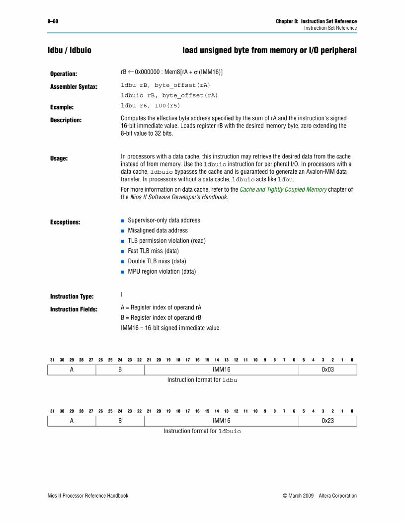
8–60 Chapter 8: Instruction Set ReferenceInstruction Set Reference
ldbu / ldbuio load unsigned byte from memory or I/O peripheral
Operation: rB ← 0x000000 : Mem8[rA + σ (IMM16)]
Assembler Syntax: ldbu rB, byte_offset(rA)
ldbuio rB, byte_offset(rA)
Example: ldbu r6, 100(r5)
Description: Computes the effective byte address specified by the sum of rA and the instruction's signed 16-bit immediate value. Loads register rB with the desired memory byte, zero extending the 8-bit value to 32 bits.
Usage: In processors with a data cache, this instruction may retrieve the desired data from the cache instead of from memory. Use the ldbuio instruction for peripheral I/O. In processors with a data cache, ldbuio bypasses the cache and is guaranteed to generate an Avalon-MM data transfer. In processors without a data cache, ldbuio acts like ldbu.
For more information on data cache, refer to the Cache and Tightly Coupled Memory chapter of the Nios II Software Developer’s Handbook.
Exceptions: ■ Supervisor-only data address
■ Misaligned data address
■ TLB permission violation (read)
■ Fast TLB miss (data)
■ Double TLB miss (data)
■ MPU region violation (data)
Instruction Type: I
Instruction Fields: A = Register index of operand rA
B = Register index of operand rB
IMM16 = 16-bit signed immediate value
31 30 29 28 27 26 25 24 23 22 21 20 19 18 17 16 15 14 13 12 11 10 9 8 7 6 5 4 3 2 1 0
A B IMM16 0x03
Instruction format for ldbu
31 30 29 28 27 26 25 24 23 22 21 20 19 18 17 16 15 14 13 12 11 10 9 8 7 6 5 4 3 2 1 0
A B IMM16 0x23
Instruction format for ldbuio
Nios II Processor Reference Handbook © March 2009 Altera CorporationPreliminary
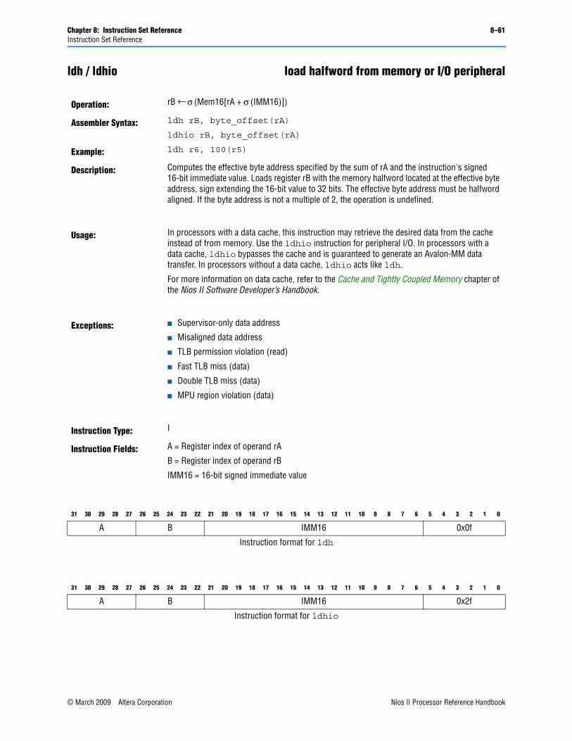
Chapter 8: Instruction Set Reference 8–61Instruction Set Reference
ldh / ldhio load halfword from memory or I/O peripheral
Operation: rB ← σ (Mem16[rA + σ (IMM16)])
Assembler Syntax: ldh rB, byte_offset(rA)
ldhio rB, byte_offset(rA)
Example: ldh r6, 100(r5)
Description: Computes the effective byte address specified by the sum of rA and the instruction's signed 16-bit immediate value. Loads register rB with the memory halfword located at the effective byte address, sign extending the 16-bit value to 32 bits. The effective byte address must be halfword aligned. If the byte address is not a multiple of 2, the operation is undefined.
Usage: In processors with a data cache, this instruction may retrieve the desired data from the cache instead of from memory. Use the ldhio instruction for peripheral I/O. In processors with a data cache, ldhio bypasses the cache and is guaranteed to generate an Avalon-MM data transfer. In processors without a data cache, ldhio acts like ldh.
For more information on data cache, refer to the Cache and Tightly Coupled Memory chapter of the Nios II Software Developer’s Handbook.
Exceptions: ■ Supervisor-only data address
■ Misaligned data address
■ TLB permission violation (read)
■ Fast TLB miss (data)
■ Double TLB miss (data)
■ MPU region violation (data)
Instruction Type: I
Instruction Fields: A = Register index of operand rA
B = Register index of operand rB
IMM16 = 16-bit signed immediate value
31 30 29 28 27 26 25 24 23 22 21 20 19 18 17 16 15 14 13 12 11 10 9 8 7 6 5 4 3 2 1 0
A B IMM16 0x0f
Instruction format for ldh
31 30 29 28 27 26 25 24 23 22 21 20 19 18 17 16 15 14 13 12 11 10 9 8 7 6 5 4 3 2 1 0
A B IMM16 0x2f
Instruction format for ldhio
© March 2009 Altera Corporation Nios II Processor Reference HandbookPreliminary
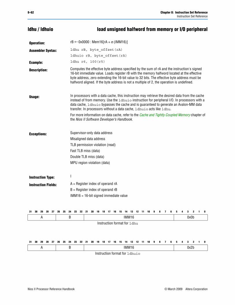
8–62 Chapter 8: Instruction Set ReferenceInstruction Set Reference
ldhu / ldhuio load unsigned halfword from memory or I/O peripheral
Operation: rB ← 0x0000 : Mem16[rA + σ (IMM16)]
Assembler Syntax: ldhu rB, byte_offset(rA)
ldhuio rB, byte_offset(rA)
Example: ldhu r6, 100(r5)
Description: Computes the effective byte address specified by the sum of rA and the instruction's signed 16-bit immediate value. Loads register rB with the memory halfword located at the effective byte address, zero extending the 16-bit value to 32 bits. The effective byte address must be halfword aligned. If the byte address is not a multiple of 2, the operation is undefined.
Usage: In processors with a data cache, this instruction may retrieve the desired data from the cache instead of from memory. Use the ldhuio instruction for peripheral I/O. In processors with a data cache, ldhuio bypasses the cache and is guaranteed to generate an Avalon-MM data transfer. In processors without a data cache, ldhuio acts like ldhu.
For more information on data cache, refer to the Cache and Tightly Coupled Memory chapter of the Nios II Software Developer’s Handbook.
Exceptions: Supervisor-only data address
Misaligned data address
TLB permission violation (read)
Fast TLB miss (data)
Double TLB miss (data)
MPU region violation (data)
Instruction Type: I
Instruction Fields: A = Register index of operand rA
B = Register index of operand rB
IMM16 = 16-bit signed immediate value
31 30 29 28 27 26 25 24 23 22 21 20 19 18 17 16 15 14 13 12 11 10 9 8 7 6 5 4 3 2 1 0
A B IMM16 0x0b
Instruction format for ldhu
31 30 29 28 27 26 25 24 23 22 21 20 19 18 17 16 15 14 13 12 11 10 9 8 7 6 5 4 3 2 1 0
A B IMM16 0x2b
Instruction format for ldhuio
Nios II Processor Reference Handbook © March 2009 Altera CorporationPreliminary
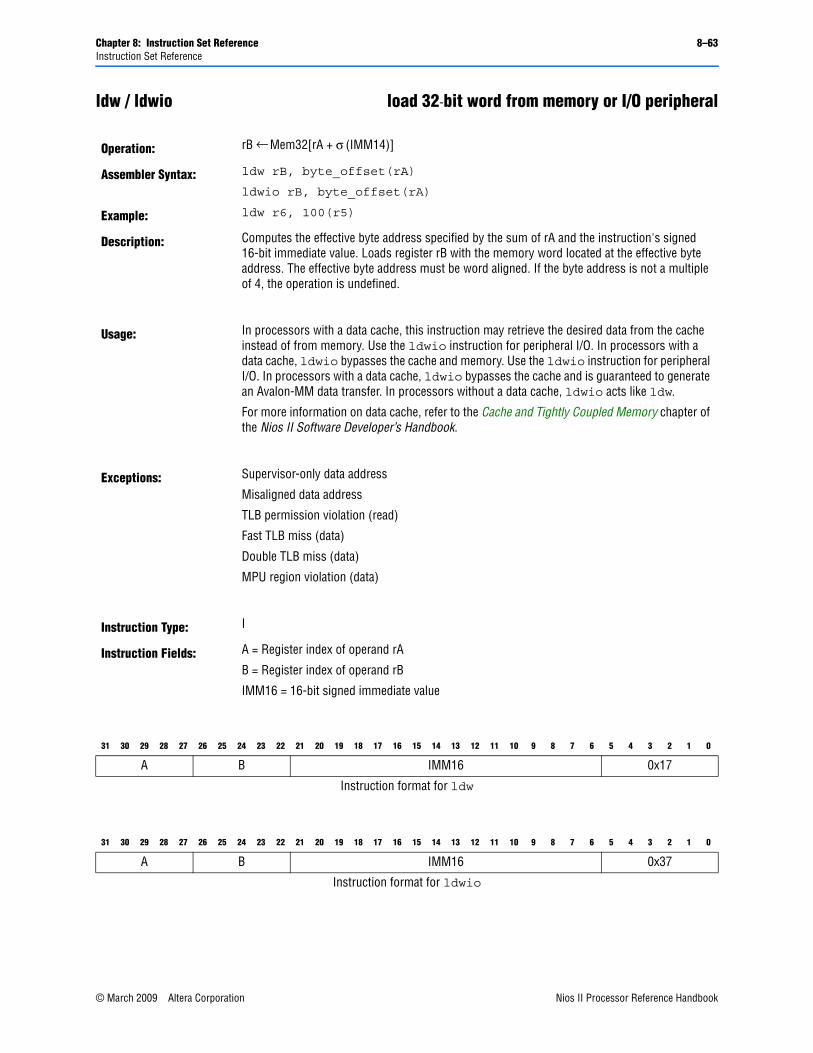
Chapter 8: Instruction Set Reference 8–63Instruction Set Reference
ldw / ldwio load 32-bit word from memory or I/O peripheral
Operation: rB ← Mem32[rA + σ (IMM14)]
Assembler Syntax: ldw rB, byte_offset(rA)
ldwio rB, byte_offset(rA)
Example: ldw r6, 100(r5)
Description: Computes the effective byte address specified by the sum of rA and the instruction's signed 16-bit immediate value. Loads register rB with the memory word located at the effective byte address. The effective byte address must be word aligned. If the byte address is not a multiple of 4, the operation is undefined.
Usage: In processors with a data cache, this instruction may retrieve the desired data from the cache instead of from memory. Use the ldwio instruction for peripheral I/O. In processors with a data cache, ldwio bypasses the cache and memory. Use the ldwio instruction for peripheral I/O. In processors with a data cache, ldwio bypasses the cache and is guaranteed to generate an Avalon-MM data transfer. In processors without a data cache, ldwio acts like ldw.
For more information on data cache, refer to the Cache and Tightly Coupled Memory chapter of the Nios II Software Developer’s Handbook.
Exceptions: Supervisor-only data address
Misaligned data address
TLB permission violation (read)
Fast TLB miss (data)
Double TLB miss (data)
MPU region violation (data)
Instruction Type: I
Instruction Fields: A = Register index of operand rA
B = Register index of operand rB
IMM16 = 16-bit signed immediate value
31 30 29 28 27 26 25 24 23 22 21 20 19 18 17 16 15 14 13 12 11 10 9 8 7 6 5 4 3 2 1 0
A B IMM16 0x17
Instruction format for ldw
31 30 29 28 27 26 25 24 23 22 21 20 19 18 17 16 15 14 13 12 11 10 9 8 7 6 5 4 3 2 1 0
A B IMM16 0x37
Instruction format for ldwio
© March 2009 Altera Corporation Nios II Processor Reference HandbookPreliminary
8–64 Chapter 8: Instruction Set ReferenceInstruction Set Reference
mov move register to register
Operation: rC ← rA
Assembler Syntax: mov rC, rA
Example: mov r6, r7
Description: Moves the contents of rA to rC.
Pseudo-instruction: mov is implemented as add rC, rA, r0.
Nios II Processor Reference Handbook © March 2009 Altera CorporationPreliminary
Chapter 8: Instruction Set Reference 8–65Instruction Set Reference
movhi move immediate into high halfword
Operation: rB ← (IMMED : 0x0000)
Assembler Syntax: movhi rB, IMMED
Example: movhi r6, 0x8000
Description: Writes the immediate value IMMED into the high halfword of rB, and clears the lower halfword of rB to 0x0000.
Usage: The maximum allowed value of IMMED is 65535. The minimum allowed value is 0. To load a 32-bit constant into a register, first load the upper 16 bits using a movhi pseudo-instruction. The %hi() macro can be used to extract the upper 16 bits of a constant or a label. Then, load the lower 16 bits with an ori instruction. The %lo() macro can be used to extract the lower 16 bits of a constant or label as shown below.
movhi rB, %hi(value)
ori rB, rB, %lo(value)
An alternative method to load a 32-bit constant into a register uses the %hiadj() macro and the addi instruction as shown below.
movhi rB, %hiadj(value)
addi rB, rB, %lo(value)
Pseudo-instruction: movhi is implemented as orhi rB, r0, IMMED.
© March 2009 Altera Corporation Nios II Processor Reference HandbookPreliminary
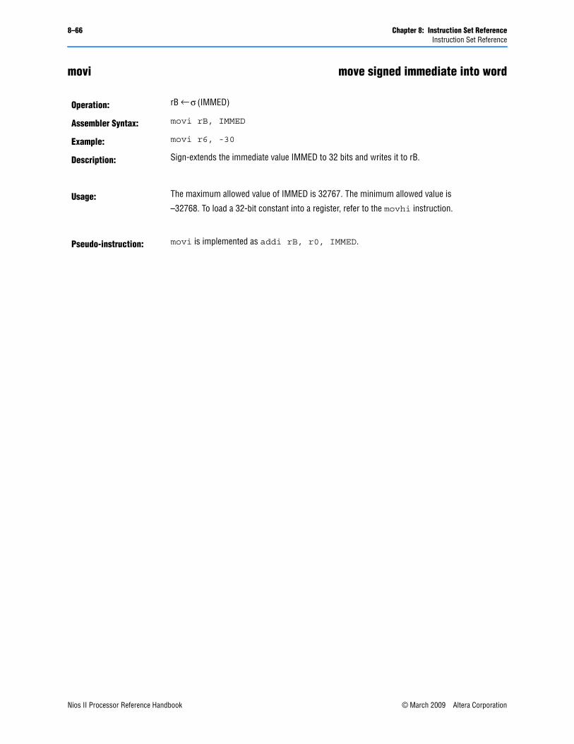
8–66 Chapter 8: Instruction Set ReferenceInstruction Set Reference
movi move signed immediate into word
Operation: rB ← σ (IMMED)
Assembler Syntax: movi rB, IMMED
Example: movi r6, -30
Description: Sign-extends the immediate value IMMED to 32 bits and writes it to rB.
Usage: The maximum allowed value of IMMED is 32767. The minimum allowed value is
–32768. To load a 32-bit constant into a register, refer to the movhi instruction.
Pseudo-instruction: movi is implemented as addi rB, r0, IMMED.
Nios II Processor Reference Handbook © March 2009 Altera CorporationPreliminary
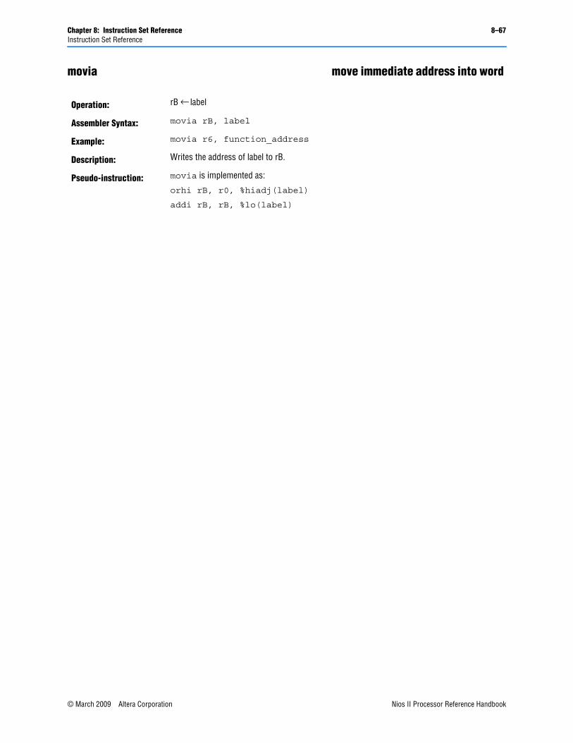
Chapter 8: Instruction Set Reference 8–67Instruction Set Reference
movia move immediate address into word
Operation: rB ← label
Assembler Syntax: movia rB, label
Example: movia r6, function_address
Description: Writes the address of label to rB.
Pseudo-instruction: movia is implemented as:
orhi rB, r0, %hiadj(label)
addi rB, rB, %lo(label)
© March 2009 Altera Corporation Nios II Processor Reference HandbookPreliminary
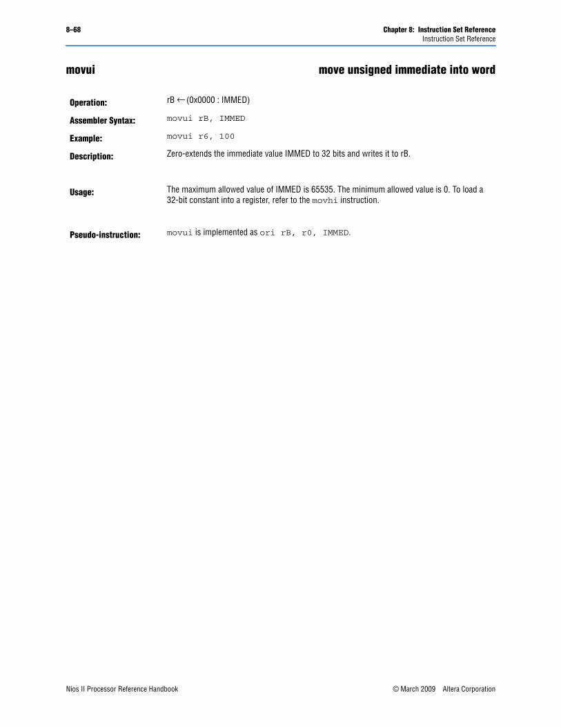
8–68 Chapter 8: Instruction Set ReferenceInstruction Set Reference
movui move unsigned immediate into word
Operation: rB ← (0x0000 : IMMED)
Assembler Syntax: movui rB, IMMED
Example: movui r6, 100
Description: Zero-extends the immediate value IMMED to 32 bits and writes it to rB.
Usage: The maximum allowed value of IMMED is 65535. The minimum allowed value is 0. To load a 32-bit constant into a register, refer to the movhi instruction.
Pseudo-instruction: movui is implemented as ori rB, r0, IMMED.
Nios II Processor Reference Handbook © March 2009 Altera CorporationPreliminary
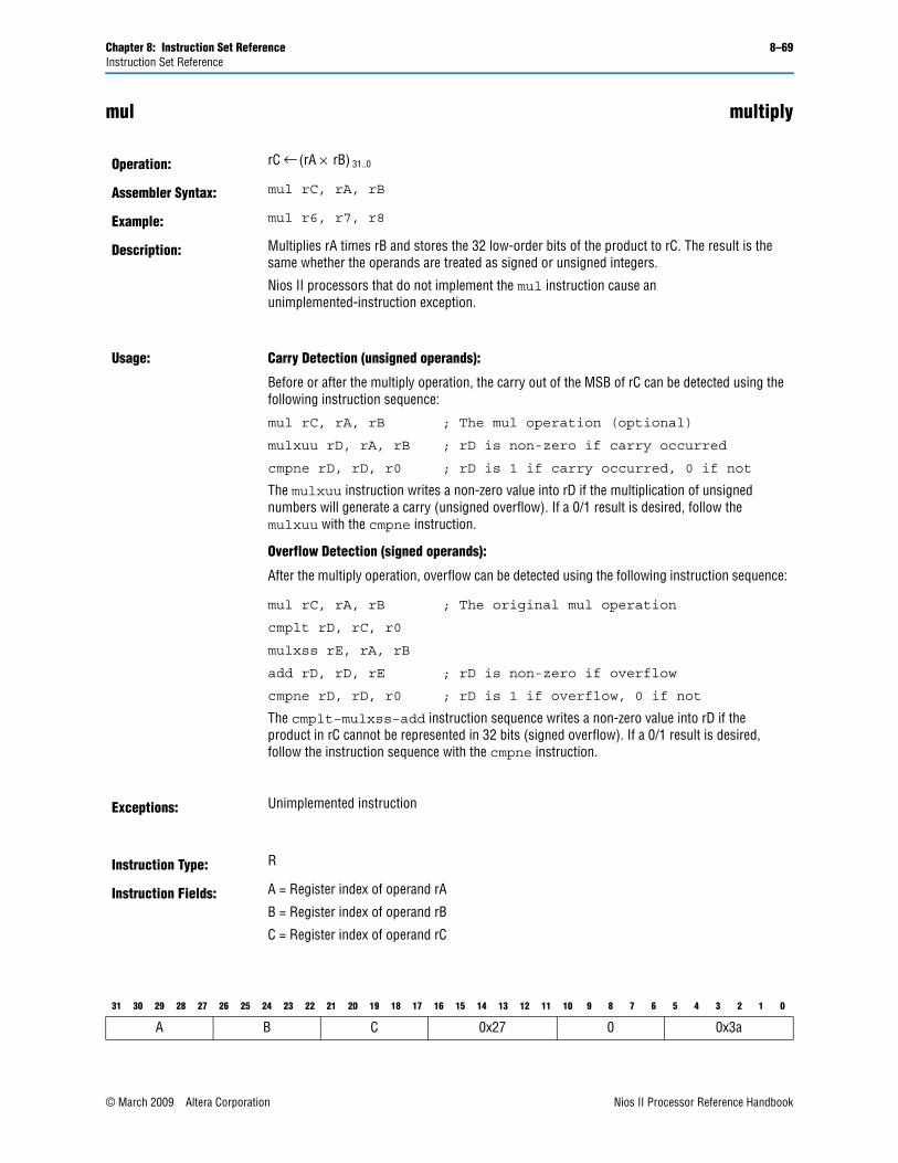
Chapter 8: Instruction Set Reference 8–69Instruction Set Reference
mul multiply
Operation: rC ← (rA × rB) 31..0
Assembler Syntax: mul rC, rA, rB
Example: mul r6, r7, r8
Description: Multiplies rA times rB and stores the 32 low-order bits of the product to rC. The result is the same whether the operands are treated as signed or unsigned integers.
Nios II processors that do not implement the mul instruction cause an unimplemented-instruction exception.
Usage: Carry Detection (unsigned operands):
Before or after the multiply operation, the carry out of the MSB of rC can be detected using the following instruction sequence:
mul rC, rA, rB
mulxuu rD, rA, rB
cmpne rD, rD, r0
; The mul operation (optional)
; rD is non-zero if carry occurred
; rD is 1 if carry occurred, 0 if not
The mulxuu instruction writes a non-zero value into rD if the multiplication of unsigned numbers will generate a carry (unsigned overflow). If a 0/1 result is desired, follow the mulxuu with the cmpne instruction.
Overflow Detection (signed operands):
After the multiply operation, overflow can be detected using the following instruction sequence:
mul rC, rA, rB
cmplt rD, rC, r0
mulxss rE, rA, rB
add rD, rD, rE
cmpne rD, rD, r0
; The original mul operation
; rD is non-zero if overflow
; rD is 1 if overflow, 0 if not
The cmplt–mulxss–add instruction sequence writes a non-zero value into rD if the product in rC cannot be represented in 32 bits (signed overflow). If a 0/1 result is desired, follow the instruction sequence with the cmpne instruction.
Exceptions: Unimplemented instruction
Instruction Type: R
Instruction Fields: A = Register index of operand rA
B = Register index of operand rB
C = Register index of operand rC
31 30 29 28 27 26 25 24 23 22 21 20 19 18 17 16 15 14 13 12 11 10 9 8 7 6 5 4 3 2 1 0
A B C 0x27 0 0x3a
© March 2009 Altera Corporation Nios II Processor Reference HandbookPreliminary
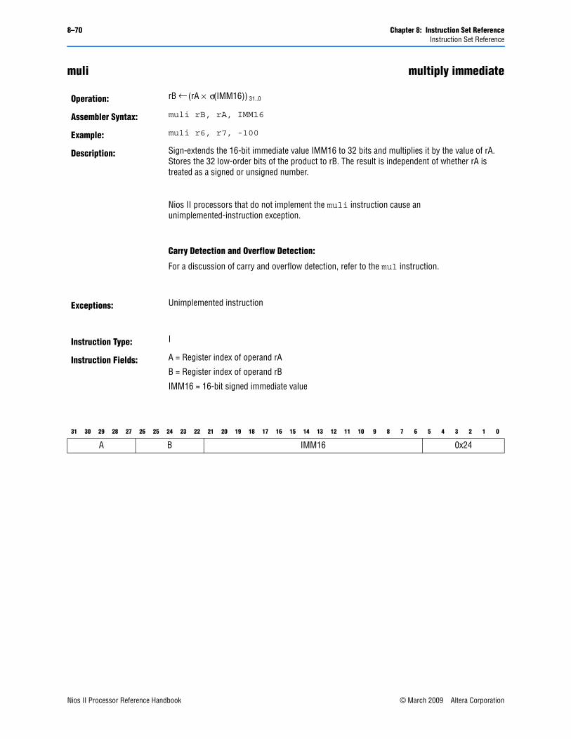
8–70 Chapter 8: Instruction Set ReferenceInstruction Set Reference
muli multiply immediate
Operation: rB ← (rA × σ(IMM16)) 31..0
Assembler Syntax: muli rB, rA, IMM16
Example: muli r6, r7, -100
Description: Sign-extends the 16-bit immediate value IMM16 to 32 bits and multiplies it by the value of rA. Stores the 32 low-order bits of the product to rB. The result is independent of whether rA is treated as a signed or unsigned number.
Nios II processors that do not implement the muli instruction cause an unimplemented-instruction exception.
Carry Detection and Overflow Detection:
For a discussion of carry and overflow detection, refer to the mul instruction.
Exceptions: Unimplemented instruction
Instruction Type: I
Instruction Fields: A = Register index of operand rA
B = Register index of operand rB
IMM16 = 16-bit signed immediate value
31 30 29 28 27 26 25 24 23 22 21 20 19 18 17 16 15 14 13 12 11 10 9 8 7 6 5 4 3 2 1 0
A B IMM16 0x24
Nios II Processor Reference Handbook © March 2009 Altera CorporationPreliminary
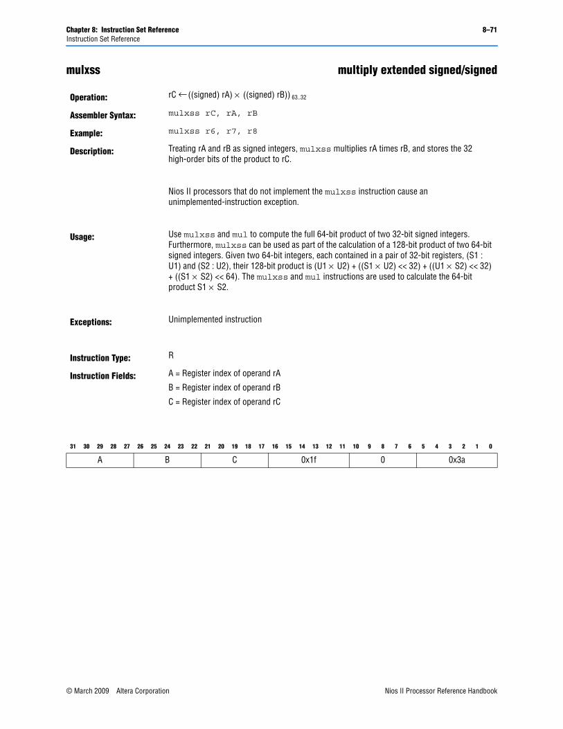
Chapter 8: Instruction Set Reference 8–71Instruction Set Reference
mulxss multiply extended signed/signed
Operation: rC ← ((signed) rA) × ((signed) rB)) 63..32
Assembler Syntax: mulxss rC, rA, rB
Example: mulxss r6, r7, r8
Description: Treating rA and rB as signed integers, mulxss multiplies rA times rB, and stores the 32 high-order bits of the product to rC.
Nios II processors that do not implement the mulxss instruction cause an unimplemented-instruction exception.
Usage: Use mulxss and mul to compute the full 64-bit product of two 32-bit signed integers. Furthermore, mulxss can be used as part of the calculation of a 128-bit product of two 64-bit signed integers. Given two 64-bit integers, each contained in a pair of 32-bit registers, (S1 : U1) and (S2 : U2), their 128-bit product is (U1 × U2) + ((S1 × U2) << 32) + ((U1 × S2) << 32) + ((S1 × S2) << 64). The mulxss and mul instructions are used to calculate the 64-bit product S1 × S2.
Exceptions: Unimplemented instruction
Instruction Type: R
Instruction Fields: A = Register index of operand rA
B = Register index of operand rB
C = Register index of operand rC
31 30 29 28 27 26 25 24 23 22 21 20 19 18 17 16 15 14 13 12 11 10 9 8 7 6 5 4 3 2 1 0
A B C 0x1f 0 0x3a
© March 2009 Altera Corporation Nios II Processor Reference HandbookPreliminary
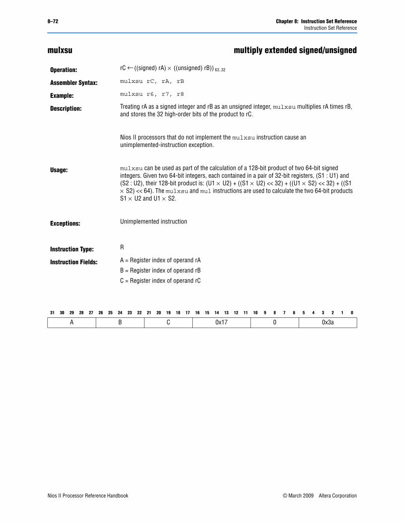
8–72 Chapter 8: Instruction Set ReferenceInstruction Set Reference
mulxsu multiply extended signed/unsigned
Operation: rC ← ((signed) rA) × ((unsigned) rB)) 63..32
Assembler Syntax: mulxsu rC, rA, rB
Example: mulxsu r6, r7, r8
Description: Treating rA as a signed integer and rB as an unsigned integer, mulxsu multiplies rA times rB, and stores the 32 high-order bits of the product to rC.
Nios II processors that do not implement the mulxsu instruction cause an unimplemented-instruction exception.
Usage: mulxsu can be used as part of the calculation of a 128-bit product of two 64-bit signed integers. Given two 64-bit integers, each contained in a pair of 32-bit registers, (S1 : U1) and (S2 : U2), their 128-bit product is: (U1 × U2) + ((S1 × U2) << 32) + ((U1 × S2) << 32) + ((S1 × S2) << 64). The mulxsu and mul instructions are used to calculate the two 64-bit products S1 × U2 and U1 × S2.
Exceptions: Unimplemented instruction
Instruction Type: R
Instruction Fields: A = Register index of operand rA
B = Register index of operand rB
C = Register index of operand rC
31 30 29 28 27 26 25 24 23 22 21 20 19 18 17 16 15 14 13 12 11 10 9 8 7 6 5 4 3 2 1 0
A B C 0x17 0 0x3a
Nios II Processor Reference Handbook © March 2009 Altera CorporationPreliminary
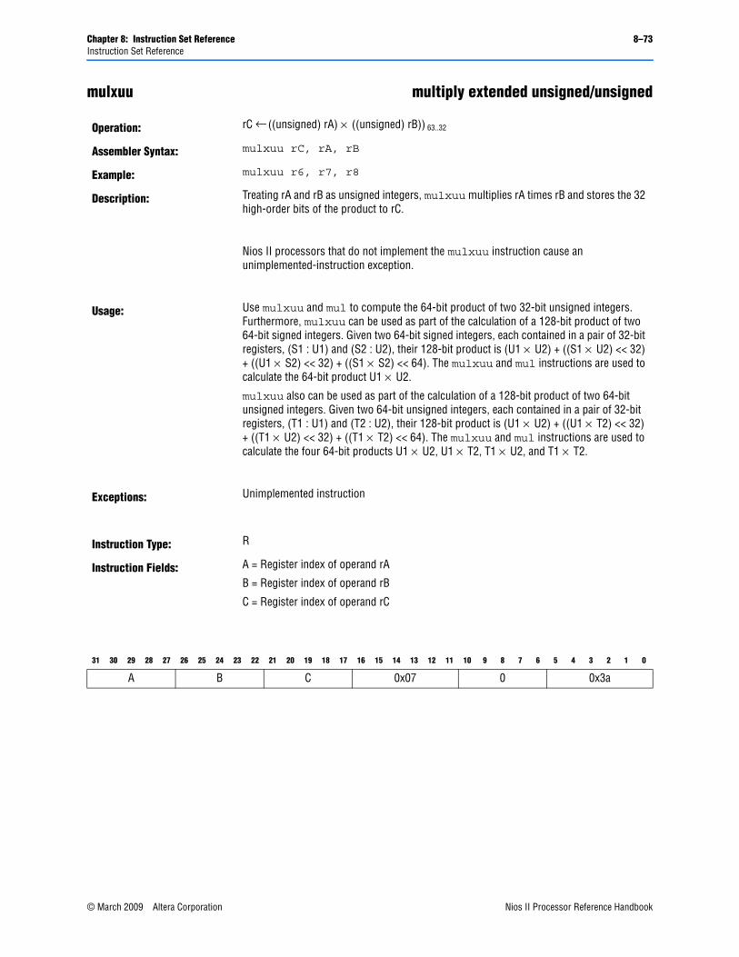
Chapter 8: Instruction Set Reference 8–73Instruction Set Reference
mulxuu multiply extended unsigned/unsigned
Operation: rC ← ((unsigned) rA) × ((unsigned) rB)) 63..32
Assembler Syntax: mulxuu rC, rA, rB
Example: mulxuu r6, r7, r8
Description: Treating rA and rB as unsigned integers, mulxuu multiplies rA times rB and stores the 32 high-order bits of the product to rC.
Nios II processors that do not implement the mulxuu instruction cause an unimplemented-instruction exception.
Usage: Use mulxuu and mul to compute the 64-bit product of two 32-bit unsigned integers. Furthermore, mulxuu can be used as part of the calculation of a 128-bit product of two 64-bit signed integers. Given two 64-bit signed integers, each contained in a pair of 32-bit registers, (S1 : U1) and (S2 : U2), their 128-bit product is (U1 × U2) + ((S1 × U2) << 32) + ((U1 × S2) << 32) + ((S1 × S2) << 64). The mulxuu and mul instructions are used to calculate the 64-bit product U1 × U2.
mulxuu also can be used as part of the calculation of a 128-bit product of two 64-bit unsigned integers. Given two 64-bit unsigned integers, each contained in a pair of 32-bit registers, (T1 : U1) and (T2 : U2), their 128-bit product is (U1 × U2) + ((U1 × T2) << 32) + ((T1 × U2) << 32) + ((T1 × T2) << 64). The mulxuu and mul instructions are used to calculate the four 64-bit products U1 × U2, U1 × T2, T1 × U2, and T1 × T2.
Exceptions: Unimplemented instruction
Instruction Type: R
Instruction Fields: A = Register index of operand rA
B = Register index of operand rB
C = Register index of operand rC
31 30 29 28 27 26 25 24 23 22 21 20 19 18 17 16 15 14 13 12 11 10 9 8 7 6 5 4 3 2 1 0
A B C 0x07 0 0x3a
© March 2009 Altera Corporation Nios II Processor Reference HandbookPreliminary
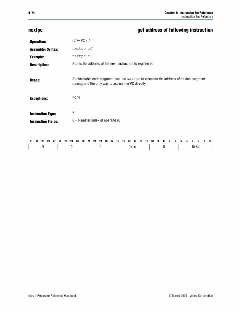
8–74 Chapter 8: Instruction Set ReferenceInstruction Set Reference
nextpc get address of following instruction
Operation: rC ← PC + 4
Assembler Syntax: nextpc rC
Example: nextpc r6
Description: Stores the address of the next instruction to register rC.
Usage: A relocatable code fragment can use nextpc to calculate the address of its data segment. nextpc is the only way to access the PC directly.
Exceptions: None
Instruction Type: R
Instruction Fields: C = Register index of operand rC
31 30 29 28 27 26 25 24 23 22 21 20 19 18 17 16 15 14 13 12 11 10 9 8 7 6 5 4 3 2 1 0
0 0 C 0x1c 0 0x3a
Nios II Processor Reference Handbook © March 2009 Altera CorporationPreliminary
Chapter 8: Instruction Set Reference 8–75Instruction Set Reference
nop no operation
Operation: None
Assembler Syntax: nop
Example: nop
Description: nop does nothing.
Pseudo-instruction: nop is implemented as add r0, r0, r0.
© March 2009 Altera Corporation Nios II Processor Reference HandbookPreliminary
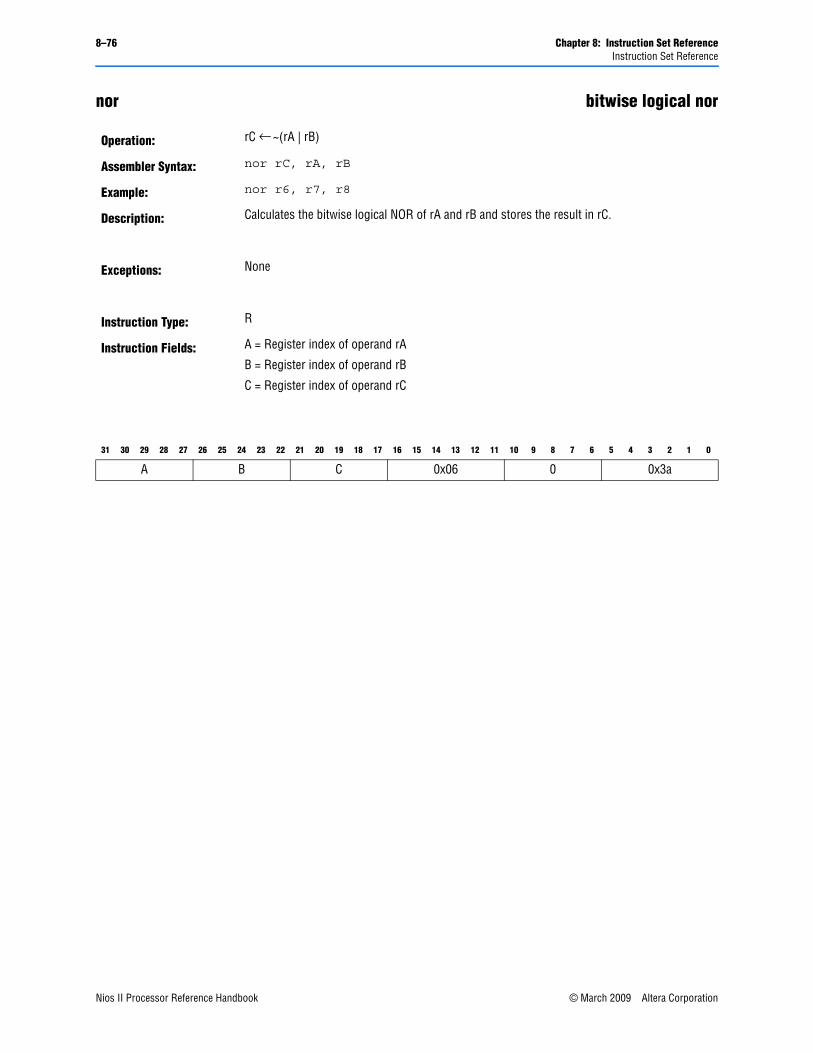
8–76 Chapter 8: Instruction Set ReferenceInstruction Set Reference
nor bitwise logical nor
Operation: rC ← ~(rA | rB)
Assembler Syntax: nor rC, rA, rB
Example: nor r6, r7, r8
Description: Calculates the bitwise logical NOR of rA and rB and stores the result in rC.
Exceptions: None
Instruction Type: R
Instruction Fields: A = Register index of operand rA
B = Register index of operand rB
C = Register index of operand rC
31 30 29 28 27 26 25 24 23 22 21 20 19 18 17 16 15 14 13 12 11 10 9 8 7 6 5 4 3 2 1 0
A B C 0x06 0 0x3a
Nios II Processor Reference Handbook © March 2009 Altera CorporationPreliminary
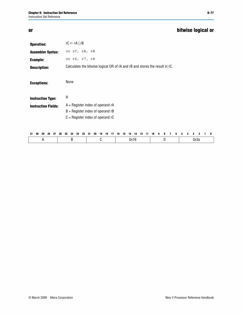
Chapter 8: Instruction Set Reference 8–77Instruction Set Reference
or bitwise logical or
Operation: rC ← rA | rB
Assembler Syntax: or rC, rA, rB
Example: or r6, r7, r8
Description: Calculates the bitwise logical OR of rA and rB and stores the result in rC.
Exceptions: None
Instruction Type: R
Instruction Fields: A = Register index of operand rA
B = Register index of operand rB
C = Register index of operand rC
31 30 29 28 27 26 25 24 23 22 21 20 19 18 17 16 15 14 13 12 11 10 9 8 7 6 5 4 3 2 1 0
A B C 0x16 0 0x3a
© March 2009 Altera Corporation Nios II Processor Reference HandbookPreliminary
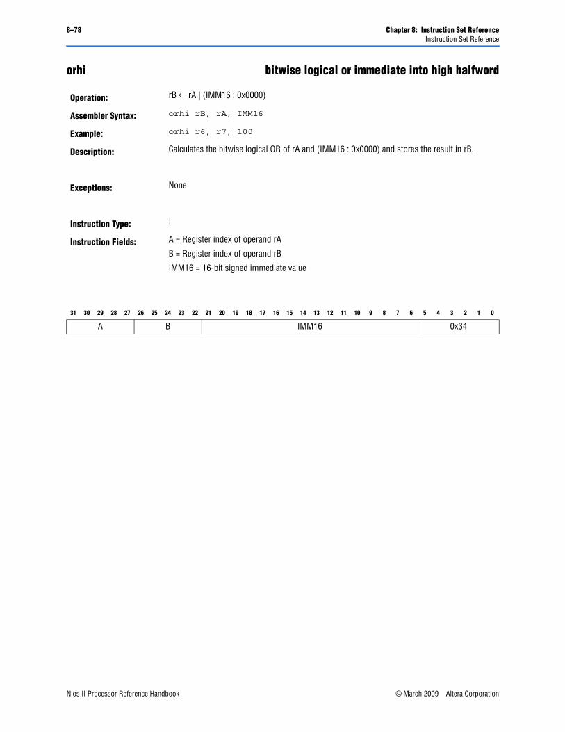
8–78 Chapter 8: Instruction Set ReferenceInstruction Set Reference
orhi bitwise logical or immediate into high halfword
Operation: rB ← rA | (IMM16 : 0x0000)
Assembler Syntax: orhi rB, rA, IMM16
Example: orhi r6, r7, 100
Description: Calculates the bitwise logical OR of rA and (IMM16 : 0x0000) and stores the result in rB.
Exceptions: None
Instruction Type: I
Instruction Fields: A = Register index of operand rA
B = Register index of operand rB
IMM16 = 16-bit signed immediate value
31 30 29 28 27 26 25 24 23 22 21 20 19 18 17 16 15 14 13 12 11 10 9 8 7 6 5 4 3 2 1 0
A B IMM16 0x34
Nios II Processor Reference Handbook © March 2009 Altera CorporationPreliminary
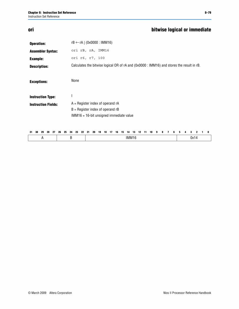
Chapter 8: Instruction Set Reference 8–79Instruction Set Reference
ori bitwise logical or immediate
Operation: rB ← rA | (0x0000 : IMM16)
Assembler Syntax: ori rB, rA, IMM16
Example: ori r6, r7, 100
Description: Calculates the bitwise logical OR of rA and (0x0000 : IMM16) and stores the result in rB.
Exceptions: None
Instruction Type: I
Instruction Fields: A = Register index of operand rA
B = Register index of operand rB
IMM16 = 16-bit unsigned immediate value
31 30 29 28 27 26 25 24 23 22 21 20 19 18 17 16 15 14 13 12 11 10 9 8 7 6 5 4 3 2 1 0
A B IMM16 0x14
© March 2009 Altera Corporation Nios II Processor Reference HandbookPreliminary
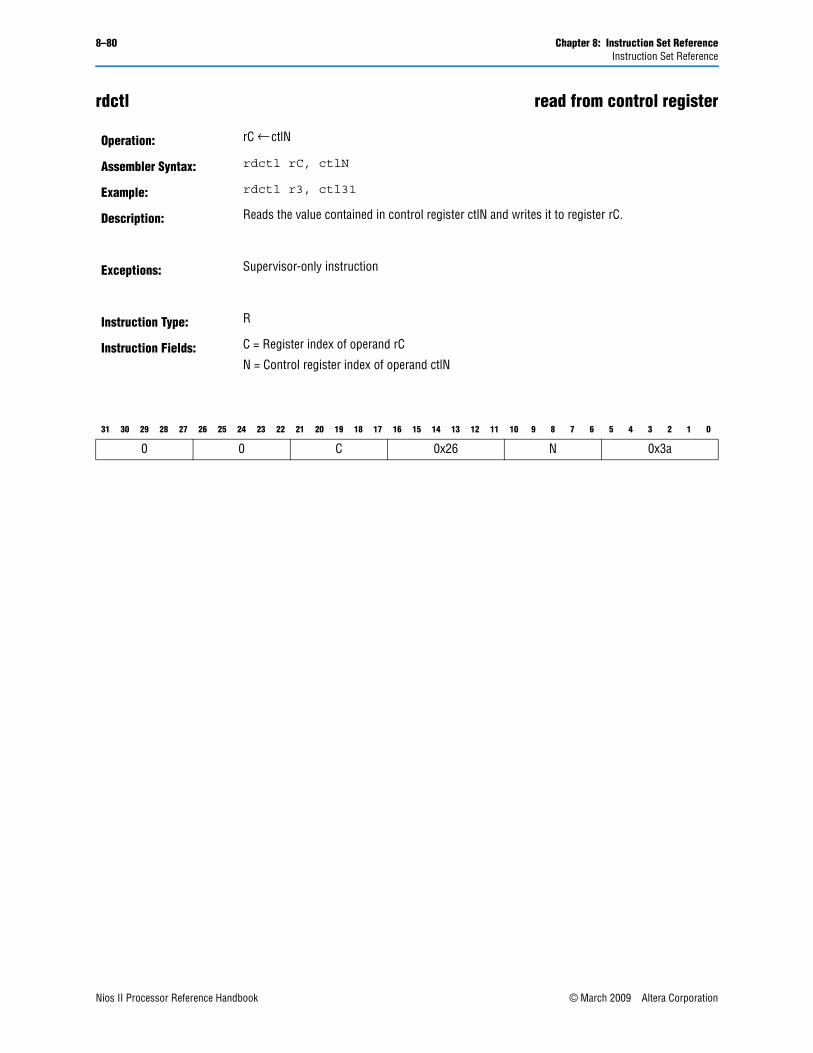
8–80 Chapter 8: Instruction Set ReferenceInstruction Set Reference
rdctl read from control register
Operation: rC ← ctlN
Assembler Syntax: rdctl rC, ctlN
Example: rdctl r3, ctl31
Description: Reads the value contained in control register ctlN and writes it to register rC.
Exceptions: Supervisor-only instruction
Instruction Type: R
Instruction Fields: C = Register index of operand rC
N = Control register index of operand ctlN
31 30 29 28 27 26 25 24 23 22 21 20 19 18 17 16 15 14 13 12 11 10 9 8 7 6 5 4 3 2 1 0
0 0 C 0x26 N 0x3a
Nios II Processor Reference Handbook © March 2009 Altera CorporationPreliminary
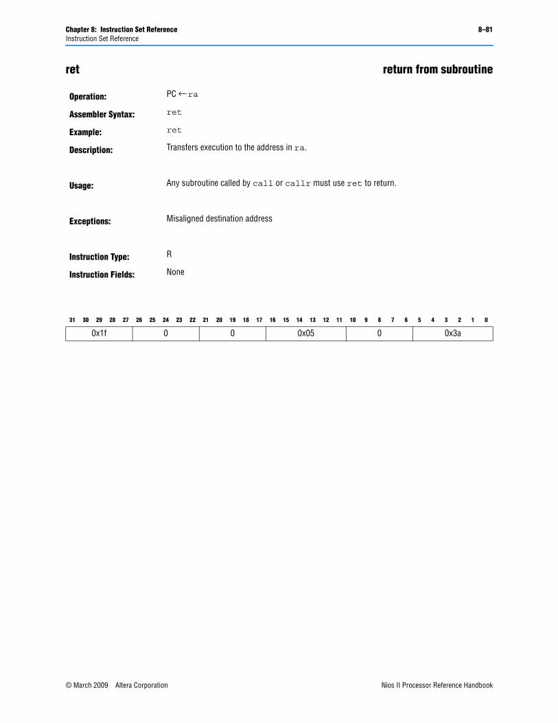
Chapter 8: Instruction Set Reference 8–81Instruction Set Reference
ret return from subroutine
Operation: PC ← ra
Assembler Syntax: ret
Example: ret
Description: Transfers execution to the address in ra.
Usage: Any subroutine called by call or callr must use ret to return.
Exceptions: Misaligned destination address
Instruction Type: R
Instruction Fields: None
31 30 29 28 27 26 25 24 23 22 21 20 19 18 17 16 15 14 13 12 11 10 9 8 7 6 5 4 3 2 1 0
0x1f 0 0 0x05 0 0x3a
© March 2009 Altera Corporation Nios II Processor Reference HandbookPreliminary
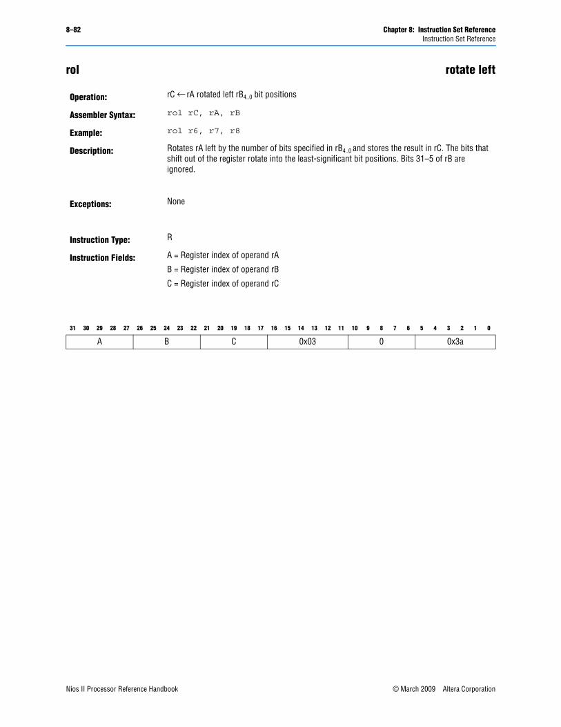
8–82 Chapter 8: Instruction Set ReferenceInstruction Set Reference
rol rotate left
Operation: rC ← rA rotated left rB4..0 bit positions
Assembler Syntax: rol rC, rA, rB
Example: rol r6, r7, r8
Description: Rotates rA left by the number of bits specified in rB4..0 and stores the result in rC. The bits that shift out of the register rotate into the least-significant bit positions. Bits 31–5 of rB are ignored.
Exceptions: None
Instruction Type: R
Instruction Fields: A = Register index of operand rA
B = Register index of operand rB
C = Register index of operand rC
31 30 29 28 27 26 25 24 23 22 21 20 19 18 17 16 15 14 13 12 11 10 9 8 7 6 5 4 3 2 1 0
A B C 0x03 0 0x3a
Nios II Processor Reference Handbook © March 2009 Altera CorporationPreliminary
Chapter 8: Instruction Set Reference 8–83Instruction Set Reference
roli rotate left immediate
Operation: rC ← rA rotated left IMM5 bit positions
Assembler Syntax: roli rC, rA, IMM5
Example: roli r6, r7, 3
Description: Rotates rA left by the number of bits specified in IMM5 and stores the result in rC. The bits that shift out of the register rotate into the least-significant bit positions.
Usage: In addition to the rotate-left operation, roli can be used to implement a rotate-right operation. Rotating left by (32 – IMM5) bits is the equivalent of rotating right by IMM5 bits.
Exceptions: None
Instruction Type: R
Instruction Fields: A = Register index of operand rA
C = Register index of operand rC
IMM5 = 5-bit unsigned immediate value
31 30 29 28 27 26 25 24 23 22 21 20 19 18 17 16 15 14 13 12 11 10 9 8 7 6 5 4 3 2 1 0
A 0 C 0x02 IMM5 0x3a
© March 2009 Altera Corporation Nios II Processor Reference HandbookPreliminary

8–84 Chapter 8: Instruction Set ReferenceInstruction Set Reference
ror rotate right
Operation: rC ← rA rotated right rB4..0 bit positions
Assembler Syntax: ror rC, rA, rB
Example: ror r6, r7, r8
Description: Rotates rA right by the number of bits specified in rB4..0 and stores the result in rC. The bits that shift out of the register rotate into the most-significant bit positions. Bits 31– 5 of rB are ignored.
Exceptions: None
Instruction Type: R
Instruction Fields: A = Register index of operand rA
B = Register index of operand rB
C = Register index of operand rC
31 30 29 28 27 26 25 24 23 22 21 20 19 18 17 16 15 14 13 12 11 10 9 8 7 6 5 4 3 2 1 0
A B C 0x0b 0 0x3a
Nios II Processor Reference Handbook © March 2009 Altera CorporationPreliminary
Chapter 8: Instruction Set Reference 8–85Instruction Set Reference
sll shift left logical
Operation: rC ← rA << (rB4..0)
Assembler Syntax: sll rC, rA, rB
Example: sll r6, r7, r8
Description: Shifts rA left by the number of bits specified in rB4..0 (inserting zeroes), and then stores the result in rC. sll performs the << operation of the C programming language.
Exceptions: None
Instruction Type: R
Instruction Fields: A = Register index of operand rA
B = Register index of operand rB
C = Register index of operand rC
31 30 29 28 27 26 25 24 23 22 21 20 19 18 17 16 15 14 13 12 11 10 9 8 7 6 5 4 3 2 1 0
A B C 0x13 0 0x3a
© March 2009 Altera Corporation Nios II Processor Reference HandbookPreliminary
8–86 Chapter 8: Instruction Set ReferenceInstruction Set Reference
slli shift left logical immediate
Operation: rC ← rA << IMM5
Assembler Syntax: slli rC, rA, IMM5
Example: slli r6, r7, 3
Description: Shifts rA left by the number of bits specified in IMM5 (inserting zeroes), and then stores the result in rC.
Usage: slli performs the << operation of the C programming language.
Exceptions: None
Instruction Type: R
Instruction Fields: A = Register index of operand rA
C = Register index of operand rC
IMM5 = 5-bit unsigned immediate value
31 30 29 28 27 26 25 24 23 22 21 20 19 18 17 16 15 14 13 12 11 10 9 8 7 6 5 4 3 2 1 0
A 0 C 0x12 IMM5 0x3a
Nios II Processor Reference Handbook © March 2009 Altera CorporationPreliminary
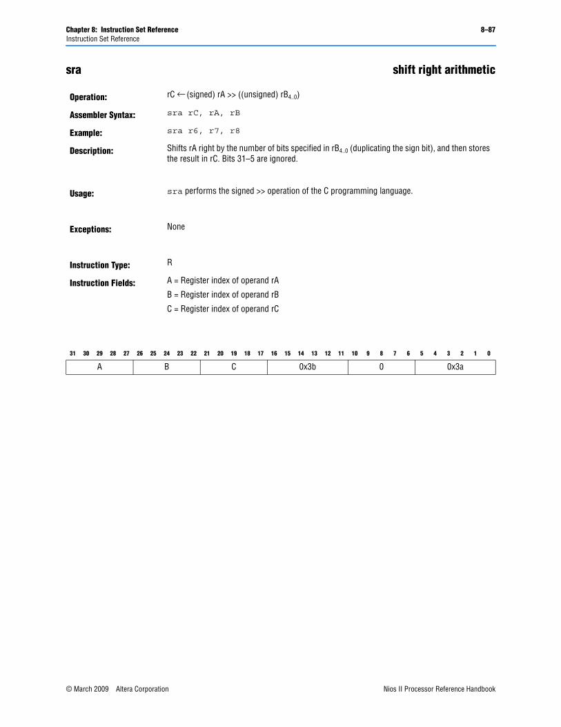
Chapter 8: Instruction Set Reference 8–87Instruction Set Reference
sra shift right arithmetic
Operation: rC ← (signed) rA >> ((unsigned) rB4..0)
Assembler Syntax: sra rC, rA, rB
Example: sra r6, r7, r8
Description: Shifts rA right by the number of bits specified in rB4..0 (duplicating the sign bit), and then stores the result in rC. Bits 31–5 are ignored.
Usage: sra performs the signed >> operation of the C programming language.
Exceptions: None
Instruction Type: R
Instruction Fields: A = Register index of operand rA
B = Register index of operand rB
C = Register index of operand rC
31 30 29 28 27 26 25 24 23 22 21 20 19 18 17 16 15 14 13 12 11 10 9 8 7 6 5 4 3 2 1 0
A B C 0x3b 0 0x3a
© March 2009 Altera Corporation Nios II Processor Reference HandbookPreliminary
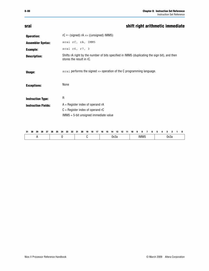
8–88 Chapter 8: Instruction Set ReferenceInstruction Set Reference
srai shift right arithmetic immediate
Operation: rC ← (signed) rA >> ((unsigned) IMM5)
Assembler Syntax: srai rC, rA, IMM5
Example: srai r6, r7, 3
Description: Shifts rA right by the number of bits specified in IMM5 (duplicating the sign bit), and then stores the result in rC.
Usage: srai performs the signed >> operation of the C programming language.
Exceptions: None
Instruction Type: R
Instruction Fields: A = Register index of operand rA
C = Register index of operand rC
IMM5 = 5-bit unsigned immediate value
31 30 29 28 27 26 25 24 23 22 21 20 19 18 17 16 15 14 13 12 11 10 9 8 7 6 5 4 3 2 1 0
A 0 C 0x3a IMM5 0x3a
Nios II Processor Reference Handbook © March 2009 Altera CorporationPreliminary
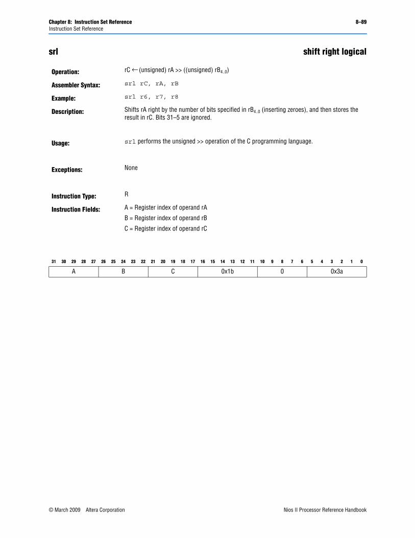
Chapter 8: Instruction Set Reference 8–89Instruction Set Reference
srl shift right logical
Operation: rC ← (unsigned) rA >> ((unsigned) rB4..0)
Assembler Syntax: srl rC, rA, rB
Example: srl r6, r7, r8
Description: Shifts rA right by the number of bits specified in rB4..0 (inserting zeroes), and then stores the result in rC. Bits 31–5 are ignored.
Usage: srl performs the unsigned >> operation of the C programming language.
Exceptions: None
Instruction Type: R
Instruction Fields: A = Register index of operand rA
B = Register index of operand rB
C = Register index of operand rC
31 30 29 28 27 26 25 24 23 22 21 20 19 18 17 16 15 14 13 12 11 10 9 8 7 6 5 4 3 2 1 0
A B C 0x1b 0 0x3a
© March 2009 Altera Corporation Nios II Processor Reference HandbookPreliminary
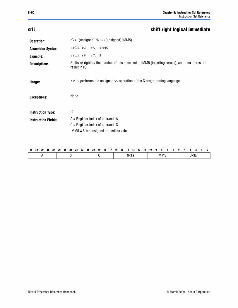
8–90 Chapter 8: Instruction Set ReferenceInstruction Set Reference
srli shift right logical immediate
Operation: rC ← (unsigned) rA >> ((unsigned) IMM5)
Assembler Syntax: srli rC, rA, IMM5
Example: srli r6, r7, 3
Description: Shifts rA right by the number of bits specified in IMM5 (inserting zeroes), and then stores the result in rC.
Usage: srli performs the unsigned >> operation of the C programming language.
Exceptions: None
Instruction Type: R
Instruction Fields: A = Register index of operand rA
C = Register index of operand rC
IMM5 = 5-bit unsigned immediate value
31 30 29 28 27 26 25 24 23 22 21 20 19 18 17 16 15 14 13 12 11 10 9 8 7 6 5 4 3 2 1 0
A 0 C 0x1a IMM5 0x3a
Nios II Processor Reference Handbook © March 2009 Altera CorporationPreliminary
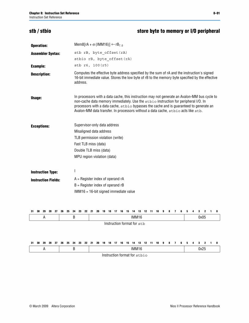
Chapter 8: Instruction Set Reference 8–91Instruction Set Reference
stb / stbio store byte to memory or I/O peripheral
Operation: Mem8[rA + σ (IMM16)] ← rB7..0
Assembler Syntax: stb rB, byte_offset(rA)
stbio rB, byte_offset(rA)
Example: stb r6, 100(r5)
Description: Computes the effective byte address specified by the sum of rA and the instruction's signed 16-bit immediate value. Stores the low byte of rB to the memory byte specified by the effective address.
Usage: In processors with a data cache, this instruction may not generate an Avalon-MM bus cycle to non-cache data memory immediately. Use the stbio instruction for peripheral I/O. In processors with a data cache, stbio bypasses the cache and is guaranteed to generate an Avalon-MM data transfer. In processors without a data cache, stbio acts like stb.
Exceptions: Supervisor-only data address
Misaligned data address
TLB permission violation (write)
Fast TLB miss (data)
Double TLB miss (data)
MPU region violation (data)
Instruction Type: I
Instruction Fields: A = Register index of operand rA
B = Register index of operand rB
IMM16 = 16-bit signed immediate value
31 30 29 28 27 26 25 24 23 22 21 20 19 18 17 16 15 14 13 12 11 10 9 8 7 6 5 4 3 2 1 0
A B IMM16 0x05
Instruction format for stb
31 30 29 28 27 26 25 24 23 22 21 20 19 18 17 16 15 14 13 12 11 10 9 8 7 6 5 4 3 2 1 0
A B IMM16 0x25
Instruction format for stbio
© March 2009 Altera Corporation Nios II Processor Reference HandbookPreliminary
8–92 Chapter 8: Instruction Set ReferenceInstruction Set Reference
sth / sthio store halfword to memory or I/O peripheral
Operation: Mem16[rA + σ (IMM16)] ← rB15..0
Assembler Syntax: sth rB, byte_offset(rA)
sthio rB, byte_offset(rA)
Example: sth r6, 100(r5)
Description: Computes the effective byte address specified by the sum of rA and the instruction's signed 16-bit immediate value. Stores the low halfword of rB to the memory location specified by the effective byte address. The effective byte address must be halfword aligned. If the byte address is not a multiple of 2, the operation is undefined.
Usage: In processors with a data cache, this instruction may not generate an Avalon-MM data transfer immediately. Use the sthio instruction for peripheral I/O. In processors with a data cache, sthio bypasses the cache and is guaranteed to generate an Avalon-MM data transfer. In processors without a data cache, sthio acts like sth.
Exceptions: Supervisor-only data address
Misaligned data address
TLB permission violation (write)
Fast TLB miss (data)
Double TLB miss (data)
MPU region violation (data)
Instruction Type: I
Instruction Fields: A = Register index of operand rA
B = Register index of operand rB
IMM16 = 16-bit signed immediate value
31 30 29 28 27 26 25 24 23 22 21 20 19 18 17 16 15 14 13 12 11 10 9 8 7 6 5 4 3 2 1 0
A B IMM16 0x0d
Instruction format for sth
31 30 29 28 27 26 25 24 23 22 21 20 19 18 17 16 15 14 13 12 11 10 9 8 7 6 5 4 3 2 1 0
A B IMM16 0x2d
Instruction format for sthio
Nios II Processor Reference Handbook © March 2009 Altera CorporationPreliminary
Chapter 8: Instruction Set Reference 8–93Instruction Set Reference
stw / stwio store word to memory or I/O peripheral
Operation: Mem32[rA + σ (IMM16)] ← rB
Assembler Syntax: stw rB, byte_offset(rA)
stwio rB, byte_offset(rA)
Example: stw r6, 100(r5)
Description: Computes the effective byte address specified by the sum of rA and the instruction's signed 16-bit immediate value. Stores rB to the memory location specified by the effective byte address. The effective byte address must be word aligned. If the byte address is not a multiple of 4, the operation is undefined.
Usage: In processors with a data cache, this instruction may not generate an Avalon-MM data transfer immediately. Use the stwio instruction for peripheral I/O. In processors with a data cache, stwio bypasses the cache and is guaranteed to generate an Avalon-MM bus cycle. In processors without a data cache, stwio acts like stw.
Exceptions: Supervisor-only data address
Misaligned data address
TLB permission violation (write)
Fast TLB miss (data)
Double TLB miss (data)
MPU region violation (data)
Instruction Type: I
Instruction Fields: A = Register index of operand rA
B = Register index of operand rB
IMM16 = 16-bit signed immediate value
31 30 29 28 27 26 25 24 23 22 21 20 19 18 17 16 15 14 13 12 11 10 9 8 7 6 5 4 3 2 1 0
A B IMM16 0x15
Instruction format for stw
31 30 29 28 27 26 25 24 23 22 21 20 19 18 17 16 15 14 13 12 11 10 9 8 7 6 5 4 3 2 1 0
A B IMM16 0x35
Instruction format for stwio
© March 2009 Altera Corporation Nios II Processor Reference HandbookPreliminary
8–94 Chapter 8: Instruction Set ReferenceInstruction Set Reference
sub subtract
Operation: rC ← rA – rB
Assembler Syntax: sub rC, rA, rB
Example: sub r6, r7, r8
Description: Subtract rB from rA and store the result in rC.
Usage: Carry Detection (unsigned operands):
The carry bit indicates an unsigned overflow. Before or after a sub operation, a carry out of the MSB can be detected by checking whether the first operand is less than the second operand. The carry bit can be written to a register, or a conditional branch can be taken based on the carry condition. Both cases are shown below.
sub rC, rA, rB
cmpltu rD, rA, rB
sub rC, rA, rB
bltu rA, rB, label
; The original sub operation (optional)
; rD is written with the carry bit
; The original sub operation (optional)
; Branch if carry was generated
Overflow Detection (signed operands):
Detect overflow of signed subtraction by comparing the sign of the difference that is written to rC with the signs of the operands. If rA and rB have different signs, and the sign of rC is different than the sign of rA, an overflow occurred. The overflow condition can control a conditional branch, as shown below.
sub rC, rA, rB
xor rD, rA, rB
xor rE, rA, rC
and rD, rD, rE
blt rD, r0, label
; The original sub operation
; Compare signs of rA and rB
; Compare signs of rA and rC
; Combine comparisons
; Branch if overflow occurred
Exceptions: None
Instruction Type: R
Instruction Fields: A = Register index of operand rA
B = Register index of operand rB
C = Register index of operand rC
31 30 29 28 27 26 25 24 23 22 21 20 19 18 17 16 15 14 13 12 11 10 9 8 7 6 5 4 3 2 1 0
A B C 0x39 0 0x3a
Nios II Processor Reference Handbook © March 2009 Altera CorporationPreliminary
Chapter 8: Instruction Set Reference 8–95Instruction Set Reference
subi subtract immediate
Operation: rB ← rA – σ (IMMED)
Assembler Syntax: subi rB, rA, IMMED
Example: subi r8, r8, 4
Description: Sign-extends the immediate value IMMED to 32 bits, subtracts it from the value of rA and then stores the result in rB.
Usage: The maximum allowed value of IMMED is 32768. The minimum allowed value is
–32767.
Pseudo-instruction: subi is implemented as addi rB, rA, -IMMED
© March 2009 Altera Corporation Nios II Processor Reference HandbookPreliminary
8–96 Chapter 8: Instruction Set ReferenceInstruction Set Reference
sync memory synchronization
Operation: None
Assembler Syntax: sync
Example: sync
Description: Forces all pending memory accesses to complete before allowing execution of subsequent instructions. In processor cores that support in-order memory accesses only, this instruction performs no operation.
Exceptions: None
Instruction Type: R
Instruction Fields: None
31 30 29 28 27 26 25 24 23 22 21 20 19 18 17 16 15 14 13 12 11 10 9 8 7 6 5 4 3 2 1 0
0 0 0 0x36 0 0x3a
Nios II Processor Reference Handbook © March 2009 Altera CorporationPreliminary
Chapter 8: Instruction Set Reference 8–97Instruction Set Reference
trap trap
Operation: estatus ← status
PIE ← 0
U ← 0
ea ← PC + 4
PC ← exception handler address
Assembler Syntax: trap
trap imm5
Example: trap
Description: Saves the address of the next instruction in register ea, saves the contents of the status register in estatus, disables interrupts, and transfers execution to the exception handler. The address of the exception handler is specified at system generation time.
The 5-bit immediate field imm5 is ignored by the processor, but it can be used by the debugger.
trap with no argument is the same as trap 0.
Usage: To return from the exception handler, execute an eret instruction.
Exceptions: Trap
Instruction Type: R
Instruction Fields: IMM5 = Type of breakpoint
31 30 29 28 27 26 25 24 23 22 21 20 19 18 17 16 15 14 13 12 11 10 9 8 7 6 5 4 3 2 1 0
0 0 0x1d 0x2d IMM5 0x3a
© March 2009 Altera Corporation Nios II Processor Reference HandbookPreliminary
8–98 Chapter 8: Instruction Set ReferenceInstruction Set Reference
wrctl write to control register
Operation: ctlN ← rA
Assembler Syntax: wrctl ctlN, rA
Example: wrctl ctl6, r3
Description: Writes the value contained in register rA to the control register ctlN.
Exceptions: Supervisor-only instruction
Instruction Type: R
Instruction Fields: A = Register index of operand rA
N = Control register index of operand ctlN
31 30 29 28 27 26 25 24 23 22 21 20 19 18 17 16 15 14 13 12 11 10 9 8 7 6 5 4 3 2 1 0
A 0 0 0x2e N 0x3a
Nios II Processor Reference Handbook © March 2009 Altera CorporationPreliminary
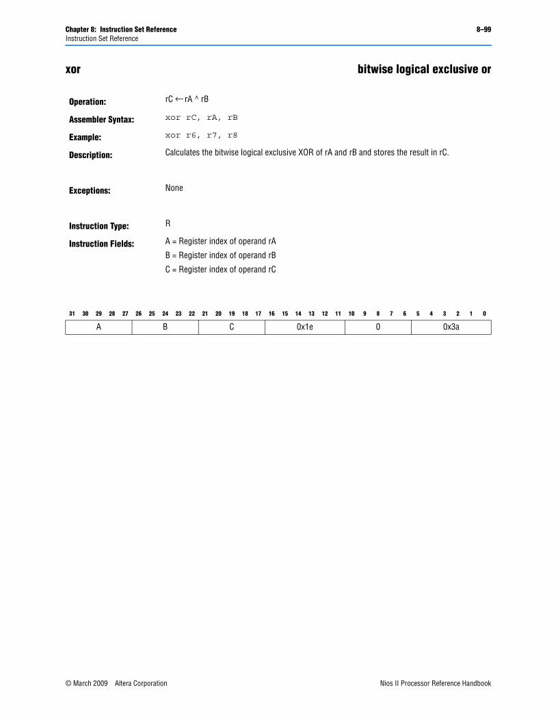
Chapter 8: Instruction Set Reference 8–99Instruction Set Reference
xor bitwise logical exclusive or
Operation: rC ← rA ^ rB
Assembler Syntax: xor rC, rA, rB
Example: xor r6, r7, r8
Description: Calculates the bitwise logical exclusive XOR of rA and rB and stores the result in rC.
Exceptions: None
Instruction Type: R
Instruction Fields: A = Register index of operand rA
B = Register index of operand rB
C = Register index of operand rC
31 30 29 28 27 26 25 24 23 22 21 20 19 18 17 16 15 14 13 12 11 10 9 8 7 6 5 4 3 2 1 0
A B C 0x1e 0 0x3a
© March 2009 Altera Corporation Nios II Processor Reference HandbookPreliminary
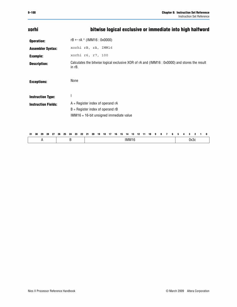
8–100 Chapter 8: Instruction Set ReferenceInstruction Set Reference
xorhi bitwise logical exclusive or immediate into high halfword
Operation: rB ← rA ^ (IMM16 : 0x0000)
Assembler Syntax: xorhi rB, rA, IMM16
Example: xorhi r6, r7, 100
Description: Calculates the bitwise logical exclusive XOR of rA and (IMM16 : 0x0000) and stores the result in rB.
Exceptions: None
Instruction Type: I
Instruction Fields: A = Register index of operand rA
B = Register index of operand rB
IMM16 = 16-bit unsigned immediate value
31 30 29 28 27 26 25 24 23 22 21 20 19 18 17 16 15 14 13 12 11 10 9 8 7 6 5 4 3 2 1 0
A B IMM16 0x3c
Nios II Processor Reference Handbook © March 2009 Altera CorporationPreliminary
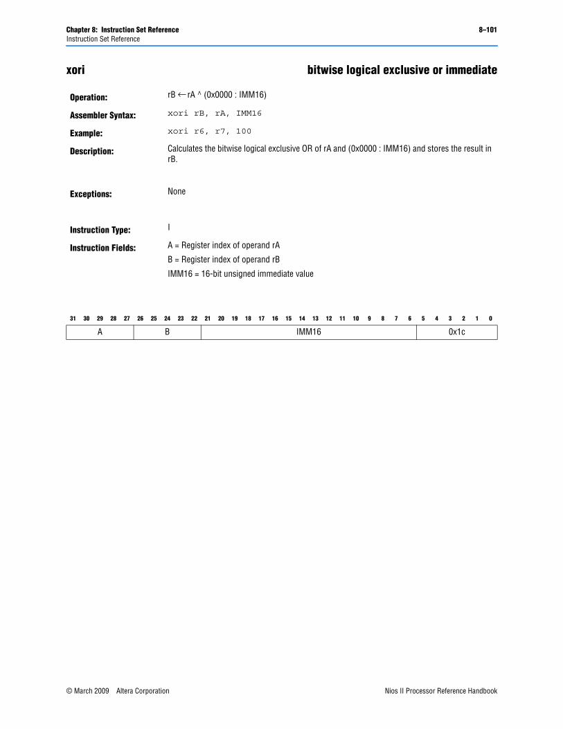
Chapter 8: Instruction Set Reference 8–101Instruction Set Reference
xori bitwise logical exclusive or immediate
Operation: rB ← rA ^ (0x0000 : IMM16)
Assembler Syntax: xori rB, rA, IMM16
Example: xori r6, r7, 100
Description: Calculates the bitwise logical exclusive OR of rA and (0x0000 : IMM16) and stores the result in rB.
Exceptions: None
Instruction Type: I
Instruction Fields: A = Register index of operand rA
B = Register index of operand rB
IMM16 = 16-bit unsigned immediate value
31 30 29 28 27 26 25 24 23 22 21 20 19 18 17 16 15 14 13 12 11 10 9 8 7 6 5 4 3 2 1 0
A B IMM16 0x1c
© March 2009 Altera Corporation Nios II Processor Reference HandbookPreliminary
8–102 Chapter 8: Instruction Set ReferenceReferenced Documents
Referenced DocumentsThis chapter references the following documents:
■ Programming Model chapter of the Nios II Processor Reference Handbook
■ Application Binary Interface chapter of the Nios II Processor Reference Handbook
■ Cache and Tightly Coupled Memory chapter of the Nios II Software Developer’s Handbook
Document Revision HistoryTable 8–6 shows the revision history for this document.
Table 8–6. Document Revision History (Part 1 of 2)
Date & Document Version Changes Made Summary of Changes
March 2009
v9.0.0
Backward-compatible change to the eret instruction B field encoding. —
November 2008
v8.1.0
Maintenance release. —
May 2008
v8.0.0
Added an Exceptions section to all instructions. Added MMU.
October 2007
v7.2.0
Added jmpi instruction. —
May 2007
v7.1.0
■ Added table of contents to Introduction section.
■ Added Referenced Documents section.
—
March 2007
v7.0.0
Maintenance release. —
November 2006
v6.1.0
Maintenance release. —
May 2006
v6.0.0
Maintenance release. —
October 2005
v5.1.0
■ Correction to the blt instruction.
■ Added U bit operation for break and trap instructions.
—
July 2005
v5.0.1
■ Added new flushda instruction.
■ Updated flushd instruction.
■ Instruction Opcode table updated with flushda instruction.
—
May 2005
v5.0.0
Maintenance release. —
December 2004
v1.2
■ break instruction update.
■ srli instruction correction.
—
Nios II Processor Reference Handbook © March 2009 Altera CorporationPreliminary
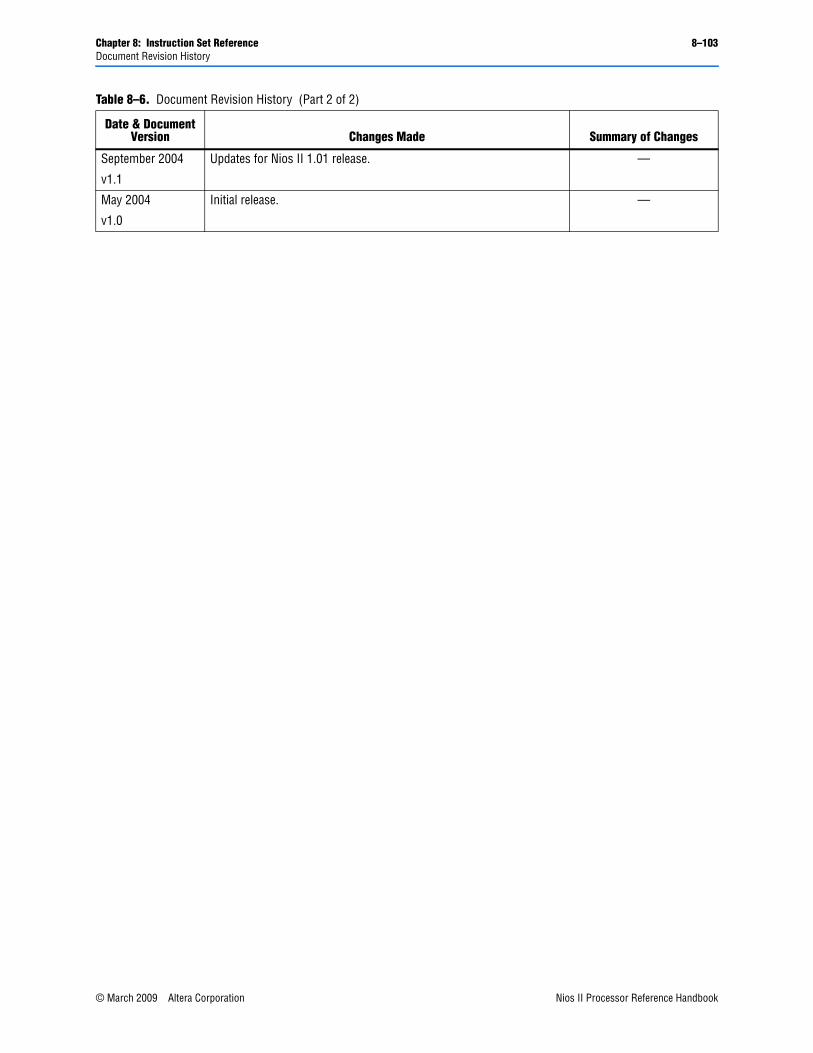
Chapter 8: Instruction Set Reference 8–103Document Revision History
September 2004
v1.1
Updates for Nios II 1.01 release. —
May 2004
v1.0
Initial release. —
Table 8–6. Document Revision History (Part 2 of 2)
Date & Document Version Changes Made Summary of Changes
© March 2009 Altera Corporation Nios II Processor Reference HandbookPreliminary

8–104 Chapter 8: Instruction Set ReferenceDocument Revision History
Nios II Processor Reference Handbook © March 2009 Altera CorporationPreliminary
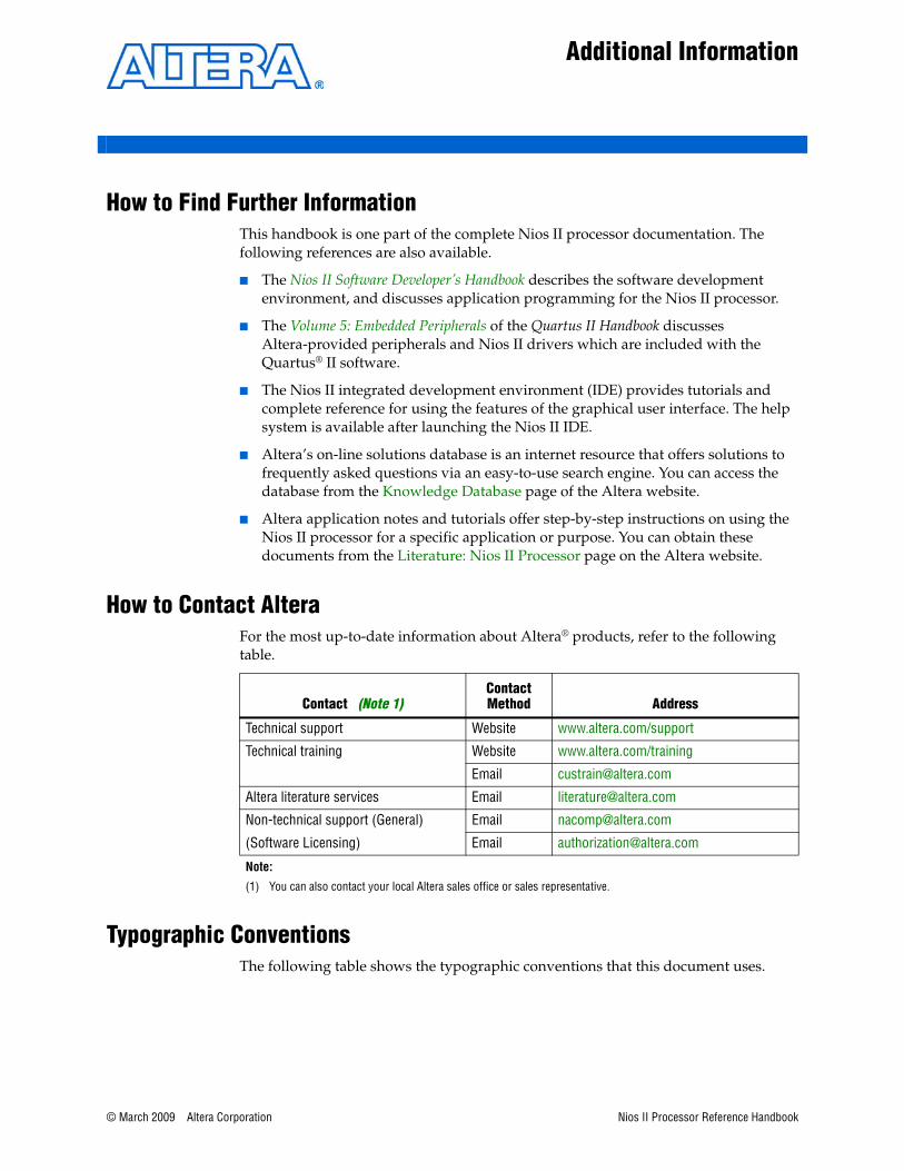
© March 2009 Altera Corporation
Additional Information
How to Find Further InformationThis handbook is one part of the complete Nios II processor documentation. The following references are also available.
■ The Nios II Software Developer’s Handbook describes the software development environment, and discusses application programming for the Nios II processor.
■ The Volume 5: Embedded Peripherals of the Quartus II Handbook discusses Altera-provided peripherals and Nios II drivers which are included with the Quartus® II software.
■ The Nios II integrated development environment (IDE) provides tutorials and complete reference for using the features of the graphical user interface. The help system is available after launching the Nios II IDE.
■ Altera’s on-line solutions database is an internet resource that offers solutions to frequently asked questions via an easy-to-use search engine. You can access the database from the Knowledge Database page of the Altera website.
■ Altera application notes and tutorials offer step-by-step instructions on using the Nios II processor for a specific application or purpose. You can obtain these documents from the Literature: Nios II Processor page on the Altera website.
How to Contact AlteraFor the most up-to-date information about Altera® products, refer to the following table.
Typographic ConventionsThe following table shows the typographic conventions that this document uses.
Contact (Note 1)Contact Method Address
Technical support Website www.altera.com/support
Technical training Website www.altera.com/training
Email [email protected]
Altera literature services Email [email protected]
Non-technical support (General) Email [email protected]
(Software Licensing) Email [email protected]
Note:
(1) You can also contact your local Altera sales office or sales representative.
Nios II Processor Reference HandbookPreliminary
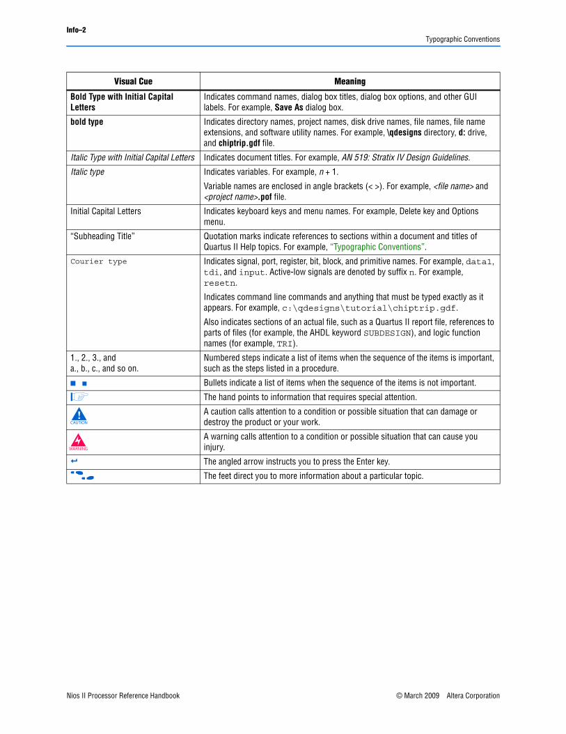
Info–2Typographic Conventions
Visual Cue Meaning
Bold Type with Initial Capital Letters
Indicates command names, dialog box titles, dialog box options, and other GUI labels. For example, Save As dialog box.
bold type Indicates directory names, project names, disk drive names, file names, file name extensions, and software utility names. For example, \qdesigns directory, d: drive, and chiptrip.gdf file.
Italic Type with Initial Capital Letters Indicates document titles. For example, AN 519: Stratix IV Design Guidelines.
Italic type Indicates variables. For example, n + 1.
Variable names are enclosed in angle brackets (< >). For example, <file name> and <project name>.pof file.
Initial Capital Letters Indicates keyboard keys and menu names. For example, Delete key and Options menu.
“Subheading Title” Quotation marks indicate references to sections within a document and titles of Quartus II Help topics. For example, “Typographic Conventions”.
Courier type Indicates signal, port, register, bit, block, and primitive names. For example, data1, tdi, and input. Active-low signals are denoted by suffix n. For example, resetn.
Indicates command line commands and anything that must be typed exactly as it appears. For example, c:\qdesigns\tutorial\chiptrip.gdf.
Also indicates sections of an actual file, such as a Quartus II report file, references to parts of files (for example, the AHDL keyword SUBDESIGN), and logic function names (for example, TRI).
1., 2., 3., and a., b., c., and so on.
Numbered steps indicate a list of items when the sequence of the items is important, such as the steps listed in a procedure.
■ ■ Bullets indicate a list of items when the sequence of the items is not important.
1 The hand points to information that requires special attention.
c A caution calls attention to a condition or possible situation that can damage or destroy the product or your work.
w A warning calls attention to a condition or possible situation that can cause you injury.
r The angled arrow instructs you to press the Enter key.
f The feet direct you to more information about a particular topic.
Nios II Processor Reference Handbook © March 2009 Altera CorporationPreliminary