Next Generation Multipurpose...
42
Next Generation Multipurpose Microprocessor Progress Report ESA Microelectronics Presentation Days March 30, 2010 www.aeroflex.com/gaisler
Transcript of Next Generation Multipurpose...

Next Generation Multipurpose Microprocessor
Progress Report
ESA Microelectronics Presentation DaysMarch 30, 2010
www.aeroflex.com/gaisler

2
Development Schedule
• Aug 2009: Kick-off
• Feb 2010: Definition and specification
• June 2010: First versions of FPGA prototypes
• Dec 2010: Final RTL code, FPGA Demonstrator
• Aug 2011: Verified ASIC netlist
• Manufacturing of prototype parts not yet decided
• Development of flight model in a separate contract

3
NGMP Key Requirements
• SPARC V8 based multi-core architecture
• Average performance of 400 MOPS on GINA benchmarks
• Minimum of 200 MOPS on any single GINA benchmark
• SPARC compliant Memory Management Unit
• Improved debug support with respect to LEON2FT
• On-chip memory >= 32 MiB
• On-chip interfaces (e.g. HSSL, SpW, PCI)
• Interface for scalable multi-processor architectures, co-processors and/or companion devices
• Maximum power consumption: 6W. Idle power 100 mW.

4
Current NGMP Definition
• Quad-core LEON4FT with GRFPU floating point units
• 128-bit L1 caches, 128-bit AHB bus
• 2-8 MiB L2 cache, 256-bit, 4-way LRU
• 64-bit DDR2-800/SDR-PC100 SDRAM memory interface
• 32 MiB on-chip DRAM (if feasible)
• 4x GRSPW2 SpaceWire cores @ 250 Mbit/s
• 32-bit, 66 MHz PCI interface
• 2x 10/100/1000 Mbit Ethernet
• 4x HSSL (if available on target technology)
• Debug links: Ethernet, JTAG, USB, dedicated SpW RMAP target

5
Architectural Overview
64-bitSDRAM
DDR2-800/SDR-PC100
L2Cache
PCIMaster
128-bit AHB @ 400 MHz
32-bit AHB @ 400 MHz
Processor bus
Slave IO bus
PROM& IO
CTRL
PROMIO
8/16-bit
HSSLSPW
USBDCL
MemoryScrubber
On-ChipSDRAM
128-bit AHB @ 400 MHz
Memory busDDR2AND
SDRAMCTRLs
UART
Timers
GPIO
DSU
AHBStatus
JTAGFPU
AHB/APBBridge
AHB/AHBBridge
PCITarget
PCIDMA
Ethernet
AHB BridgeIOMMU
AHB/AHBBridge
32-bit AHB @ 400 MHz Master IO bus
32-bit AHB @ 400 MHz
Debug bus
32-bit APB @ 400 MHz
RMAPDCL
AHBStatus
PCIArbiter
EthernetSPWSPWSPWHSSLHSSLHSSL
UART
S S S S S S
SS
S
S
S
S
SM
SMM
M
M MMM
MM
M
MM
S
S S S
M = Master interface(s)S = Slave interface(s)X = Snoop interface
X
X
MX
S
X
M
SM
S
S
S
Caches MMU
TimersIRQCTRL
LEON4FT
FPU
MX
Caches MMU
TimersIRQCTRL
LEON4FT
FPU
Caches MMU
Timers IRQCTRL
LEON4FT
FPU
Caches MMU
Timers IRQCTRL
LEON4FT
IRQMPIRQCTRL1 IRQCTRL2 IRQCTRL3 IRQCTRL4
IRQSTAMP
S
S S S S S
MX MX

6
The NGMP will have improved debugging support compared to
the LEON2FT and many existing LEON3 implementations. The
new features include:
● Several high-speed debug interfaces● Non-intrusive debugging through dedicated Debug bus● AHB trace buffer with filtering● Instruction trace buffer with filtering● Hardware data watchpoints● Data area monitoring
Improved Debugging Support

7
Improved Profiling Support
The NGMP has improved profiling support compared to the LEON2FT and LEON3. The new features allow to measure the following metrics:
● Processor performance and L1 cache hit rate● AHB utilization● L2 cache hit rate

8
● JTAG Debug Communication Link● Modest bandwidth, 500 kb/s● Easy to use
● RMAP target● Bandwidth: 20 Mb/s● Provides DSU access over SpW
● USB Debug Communication Link● Bandwidth: 20 Mb/s● Very easy to interface
● Ethernet Debug Links● Bandwidth: 100 Mb/s● Popular among AG customers● Can optionally be connected to master I/O bus
Debug Communication Links

9
● Features in NGMP not found in most present day LEON/LEON-MP architectures:
● LEON4FT● L2 cache with locking● Large on-chip RAM (32 MiB, if available on target)● Wider AMBA buses● Better support for partitioning:
● IOMMU● Per-processor timers and interrupt cntrlrs
● Improved debug support (# links, filters, perf. cnt)● Improved support for AMP● Boot options (PROM, RMAP)● Interrupt time stamping● Hardware memory scrubber
Summary of New Features

10
● Baseline is ST 65nm space technology
● Requirements● DDR2 PHY● I/O standards: LVTTL, SSTL-I, PCI● Memory:
● 1-port RAM, 2-port RAM● High density 1-port RAM/SDRAM
● Backup options:● UMC 90 nm with DARE library● Tower 130 nm with Ramon library
Target technology
11
Choices that are still open include:
● On-chip DRAM (desirable but not likely to be included)
● 2 or 4 CPU cores
● Shared or individual FPUs (3 possible configurations)
● External memory type (DDR/DDR2)
● Configurable SDRAM width (32/64 data bits)
● L1/L2 cache size
● IOMMU implementation
● High-speed interfaces
● Different frequencies of processor bus and other buses
● Spare-column of external memory
Selection of Open Items

12
● Operating systems that will be ported in this activity:● RTEMS 4.8 and 4.10● WindRiver VxWorks 6.7 with SMP support● eCos 2.0 ● Linux 2.6
● Other OSs already ported to LEON include:● LynxOS (LynuxWorks)● ThreadX (Express Logic)● Nucleus (Mentor Graphics)
Operating Systems

13
● The GNU C/C++ toolchain will be used● Versions 4.1.2 and 4.4.2 have been successfully tested● OpenMP requires GCC 4.4+ and a pthreads
implementation
● RTEMS 4.8 uses GCC 4.2.4, RTEMS 4.10 uses GCC 4.4
● VxWorks 6.7 uses GCC 4.1.1
● Mkprom2 with support for booting AMP systems
Toolchain

14
• NGMP simulator based on GRSIM
• C models of IP cores linked into a final simulator
– LEON4
– L2 cache and DDR memory interface
– GRSPW, GRETH, GRPCI
• Reentrant and thread safe library
• Accuracy goal is above 90% over an extended simulation period
Simulator

15
● Preliminary version of ISS delivered● AHB bridges have been extended with read/write
combining/splitting● LEON4 has been validated with two of the possible
GRFPU configurations● Validation work of new PCI core is progressing● Extensions (MEMPROT, FT, etc.) of L2 cache started● Work on the IOMMU has been started● Development of memory scrubber has been started● Investigations into prototype possibilities
Current progress

16
● Investigations into ASIC prototypes is currently ongoing● FPGA prototypes with reduced NGMP designs (June 2010)
● Xilinx ML510● Synopsys HAPS-51● Aeroflex Gaisler GR-CPCI-XC4V with LX200 FPGA
Prototypes

17
Thank you for listening
For updates and to download the NGMP specification, please see:
http://microelectronics.esa.int/ngmp/ngmp.htm

18
Extra slides

19
LEON4

20
● IEEE-1754 SPARC V8 compliant 32-bit processor● 7-stage pipeline, multi-processor support● Separate multi-set L1 caches with LRU/LRR/RND● Configurable L2 cache, 256-bit internal, 1 – 4 ways● 64-bit single-clock load/store operation● 64-bit 4 port register file● 64- or 128-bit AHB bus interface● Branch prediction● On-chip debug support unit with trace buffer● 1.7 DMIPS/MHz, 0.6 Wheatstone MFLOPS/MHz● Estimated 0.35 SPECINT/MHz, 0.25 SPECFP/MHz● 2.1 CoreMark/MHz (comparable to ARM11)
LEON4 / GRFPU / L2 cache

21
● SPARC V8 compatible core with CAS support● 64-bit register file with BCH● 64-bit load/store operation with on-the-fly correction● Static branch prediction● Write-combining store buffer● 64- or 128-bit caches with 4-bit parity● 64- or 128-bit AHB bus interface● Performance counters● Local timer and interrupt controller● 1.7 Dhrystone MIPS/MHz, 0.6 Wheatstone MFLOPS/MHz● 0.35 SPECINT/MHz, 0.25 SPECFP/MHz, 2.1 CoreMark/MHz
LEON4FT Overview

22
● L2 cache configurable with 1 - 4 ways, any size● 256-bit internal cache line with 64-bit BCH ECC● Copy-back and write-through operation● 0-waitstate pipelined write, 3/4-waitstates read hit● Essential for SMP performance scaling● Reduces effects of slower memory (SDRAM) if DDR2
cannot be used
L2 Cache

23
Other NGMP Components

24
● Primary memory interface: DDR2/SDRAM● DDR2-800/SDRAM PC100● 64-bit data● 16 and 32 bit Reed-Solomon ECC● Corrects two or four 4-bit errors
● On-chip SDRAM (if available on target tech.)● Performance:
Memory bus memory controllers
Interface Cache line fetch(ns)
Sustainable bandwidth(Mb/s)
Min sys freq.(MHz)
Max sys. freq.(MHz)
SDRAM PC100 100 320 - 400
DDR2-800 42.5 512 62.5 400

25
● Can access external DDR2/SDRAM and on-chip SDRAM● Performs the following operations:
● Initialization● Scrubbing● Memory re-generation
● Configurable by software● Counts correctable errors with option to alert CPU● User can define data pattern used for initialization● Can initialize the entire 2 GiB main memory area in less
than four seconds
Memory scrubber

26
● Connects all DMA capable I/O master through one interface onto the Processor bus
● Performs pre-fetching and read/write combining● Provides address translation and access restriction● Interface will be similar to existing solution● Will not be required to use the same page tables as the
processor● Master can be placed in groups where each group can
have its own set of page tables● Exact definition postponed since prototyping has been
deemed necessary● Likely candidate to base IOMMU on: sun4m
Uni-directional AHB bridge with IOMMU

27
● 4x GRSPW2 cores● Maximum link bit rate will be at least 200 Mb/s● Hardware RMAP target in each core● Two ports per core (redundant port)● Core buffers will be implemented with registers● Each core has its own DMA engine
Spacewire

28
● 2x Ethernet interfaces● Supports 10/100/1000 Mbit in both full- and half-duplex● DMA engine for both receiver and transmitter● Internal buffer allows core to buffer a complete packet● Supports MII and GMII interfaces to connect an external
transceiver● Supports scatter gather I/O and IPv4 checksum
offloading● Provides Ethernet Debug Communication Link● EDCL also connected to debug bus● 2 KiB EDCL buffer → 100 Mb/s● Soft configurable EDCL IP/MAC addresses
Gigabit Ethernet
DDR264-bit
DDR2-800
L2Cache
LEON4FT
PCIMaster
128-bit AHB @ 400 MHz
32-bit AHB @ 400 MHz
Processor bus
Slave IO bus
PROM& IOCTRL
PROMIO
8/16-bit
HSSLSPW
USBDCL
FPUMemoryScrubber
On-ChipSDRAM
128-bit AHB @ 400 MHz
Memory bus
DDR2CTRL
UART
Timers
GPIO
DSU
AHBStatus
JTAG
LEON4FT LEON4FT FPU LEON4FT
AHB/APBBridge
AHB/AHBBridge
PCITarget
PCIDMA Ethernet
AHB BridgeIOMMU
AHB/AHBBridge
32-bit AHB @ 400 MHz
Master IO bus
32-bit AHB @ 400 MHz
Debug bus
32-bit APB @ 400 MHz

29
● Provides PCI target interface● 32-bit interface supporting 66 MHz operation● Target DMA interface is placed on the Master I/O bus
while the AHB slave interface is on the Slave I/O bus● Target has two bars of sizes 256 MiB and 64 MiB● Specification based on GRPCI core. AG is currently
developing a new core which is planned to replace GRPCI.
PCI interface
30
● Inclusion of HSSL depends on availability of macros on target technology
● ESA requires Spacefibre to be instantiated in the NGMP, this will be done if working IP is made available
● As backup, a simple descriptor based DMA cored based on GRETH_GBIT or GRSPW2 could be used
● Little is currently known regarding the HSSL, however as long as the backend has a AMBA 2.0 compliant interface there should be nothing to prevent its inclusion
High-Speed Serial Link

31
● Specified to support AMP and SMP● Internal processor interrupt controllers● Shared multiprocessor interrupt controller (IRQMP)● 4x secondary interrupt controllers● General topology:
Interrupt infrastructure
IRQMP
LEON4FT LEON4FT LEON4FT LEON4FT
SecondaryIRQCTRL 1
SecondaryIRQCTRL 2
SecondaryIRQCTRL 3
SecondaryIRQCTRL 4

32
● IRQMP is connected to each processor● Each processor has an internal interrupt controller (not
used when the processor core is listening to IRQMP)● Each secondary interrupt controller is connected to
IRQMP and to each internal interrupt controller.
Interrupt infrastructure Cont..
IRQMP
LEON4FT LEON4FT LEON4FT LEON4FT
SecondaryIRQCTRL 1
SecondaryIRQCTRL 2
SecondaryIRQCTRL 3
SecondaryIRQCTRL 4

33
● All internal interrupt controllers are disabled● Processor cores listen to IRQMP● Mask register in IRQMP is used to listen to one or several
of the secondary interrupt controllers
SMP Configuration
IRQMP
LEON4FT LEON4FT LEON4FT LEON4FT
SecondaryIRQCTRL 1
SecondaryIRQCTRL 2
SecondaryIRQCTRL 3
SecondaryIRQCTRL 4
34
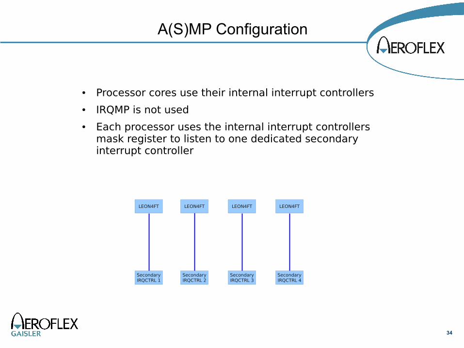
LEON4FT LEON4FT LEON4FT LEON4FT
SecondaryIRQCTRL 1
SecondaryIRQCTRL 2
SecondaryIRQCTRL 3
SecondaryIRQCTRL 4
● Processor cores use their internal interrupt controllers● IRQMP is not used● Each processor uses the internal interrupt controllers
mask register to listen to one dedicated secondary interrupt controller
A(S)MP Configuration

35
● Infrastructure also allows mixed configurations:● 1x SMP + (1x or 2x) AMP
● Synchronization via interrupts can be achieved via IRQMP or by writing the force register of a secondary interrupt controller
● Specified system has 48 interrupt lines allocated.● Each configuration has the same view of the interrupt
lines (local timers only available to the processor in which they are located)
Interrupt infrastructure round-up

36
Operating Systems

37
VxWorks
• Version 6.7
• Support for Symmetrical Multiprocessing
• Develop BSP support for per CPU timers and interrupt controllers
• Device drivers for SpaceWire, Ethernet and PCI

38
RTEMS
• We will support both 4.8 and 4.10
• Develop BSP support for per CPU timers and interrupt controllers
• Support RTEMS Asymmetrical Multiprocessing (AMP)
• Device drivers for SpaceWire, Ethernet and PCI

39
VxWorks
• Version 6.7
• Support for Symmetrical Multiprocessing (SMP)
• Support for protection through MMU
• Device drivers for SpaceWire, Ethernet and PCI
• Develop BSP support for per CPU timers and interrupt controllers
• If time permits look into VxWorks MP for AMP support

40
eCos 2.0
• Version 2.0 will be used in NGMP. Later versions exhibit SMP problems
• Support for SMP
• Device drivers for SpaceWire, Ethernet and PCI

41
Linux 2.6
• Process protection through MMU
• SMP support
• IOMMU support
• Device drivers for SpaceWire, Ethernet and PCI

42
• Possible to support paravirtualized hypervisors such as:
– L4
– Xtratum
– WindRiver Hypervisor
– SysGo PikeOS
• Guest OSes must be ported to the hypervisor
• No hypervisor will be ported in the NGMP activity
Virtualization