
Next-generation crossover-free quantum Hall arrays with ...
12
1 Next-generation crossover-free quantum Hall arrays with superconducting interconnections Mattias Kruskopf 1,2 , Albert F. Rigosi 1 , Alireza R. Panna 1 , Martina Marzano 4 , Dinesh Patel 3 , Hanbyul Jin 1,2 , David B. Newell 1 , and Randolph E. Elmquist 1 1 National Institute of Standards and Technology (NIST), Gaithersburg, MD 20899, USA 2 Joint Quantum Institute, University of Maryland, College Park, MD 20742, USA 3 Department of Physics, National Taiwan University, Taipei 10617, Taiwan 4 Politecnico di Torino, Istituto Nazionale di Ricerca Metrologica, Turin, Italy E-mail: [email protected], [email protected], [email protected], [email protected], [email protected], [email protected], [email protected] and [email protected] Keywords: quantum Hall effect, quantized Hall array resistance standards, epitaxial graphene, superconducting contacts, multiple connection, split contacts Abstract: This work presents precision measurements of quantized Hall array resistance devices using superconducting, crossover-free, multiple interconnections as well as graphene split contacts. These new techniques successfully eliminate the accumulation of internal resistances and leakage currents that typically occur at interconnections and crossing leads between interconnected devices. As a result, a scalable quantized Hall resistance array is obtained with a nominal value that is as precise and stable as that from single-element quantized Hall resistance standards. 1. Introduction Although the first graphene samples were isolated as micrometer-size flakes and found to have favorable electrical and optical properties,[1–5], more recently, high-quality and centimeter-scale graphene has been obtained through epitaxial growth on silicon carbide (SiC) [6–9]. The epitaxial graphene (EG) growth has improved to the point that one can realize devices suitable for general applications, like larger scale electronics, and more specialized applications, such as quantized Hall resistance (QHR) standards [9–17].
Transcript of Next-generation crossover-free quantum Hall arrays with ...

1
Next-generation crossover-free quantum Hall arrays with superconducting
interconnections
Mattias Kruskopf1,2, Albert F. Rigosi1, Alireza R. Panna1, Martina Marzano4,
Dinesh Patel3, Hanbyul Jin1,2, David B. Newell1, and Randolph E. Elmquist1
1National Institute of Standards and Technology (NIST), Gaithersburg, MD 20899, USA
2Joint Quantum Institute, University of Maryland, College Park, MD 20742, USA
3Department of Physics, National Taiwan University, Taipei 10617, Taiwan
4Politecnico di Torino, Istituto Nazionale di Ricerca Metrologica, Turin, Italy
E-mail: [email protected], [email protected],
[email protected], [email protected], [email protected], [email protected], [email protected] and [email protected]
Keywords: quantum Hall effect, quantized Hall array resistance standards, epitaxial
graphene, superconducting contacts, multiple connection, split contacts
Abstract: This work presents precision measurements of quantized Hall array resistance
devices using superconducting, crossover-free, multiple interconnections as well as
graphene split contacts. These new techniques successfully eliminate the accumulation of
internal resistances and leakage currents that typically occur at interconnections and
crossing leads between interconnected devices. As a result, a scalable quantized Hall
resistance array is obtained with a nominal value that is as precise and stable as that from
single-element quantized Hall resistance standards.
1. Introduction
Although the first graphene samples were isolated as micrometer-size flakes and found to
have favorable electrical and optical properties,[1–5], more recently, high-quality and
centimeter-scale graphene has been obtained through epitaxial growth on silicon carbide (SiC)
[6–9]. The epitaxial graphene (EG) growth has improved to the point that one can realize devices
suitable for general applications, like larger scale electronics, and more specialized applications,
such as quantized Hall resistance (QHR) standards [9–17].

2
Limitations of reliable access to quantum Hall resistance plateaus other than RH = RK/2 =
h/2e2, where RH is the Hall resistance, and RK is the von Klitzing constant, have motivated the
development of quantum Hall array resistance standards (QHARS) based on series and in
parallel connected devices [18–20]. These next-generation quantum resistance devices show
promise in fulfilling the requirement of scalability for future applications in metrology. One issue
for these scalable resistance networks, based on many Hall bar elements, is that they may suffer
from accumulated internal resistances and Hall resistance contributions at thin-film metal
contacts and interconnections. In addition, the crossover of electrical connections between Hall
elements introduce other difficulties such as possible leakage currents through the dielectric
where the voltage terminals need to cross the current path. Finally, because of limited chip
mounting options, it is impossible to realize longitudinal resistance measurements as
recommended in metrological guidelines for the QHR [21]. These challenges are the reason why
state-of-the-art QHARS devices often cannot reach the level of quantization needed for
resistance metrology.
In this work, we present new EG-based QHARS device design approaches to minimize the
error contributions of undesired resistances at contacts and interconnections and ensure precise
resistance quantization for series-parallel networks. The applied split contact geometry and
superconducting interconnections ensure minimum deviation from the nominal resistance value
on the order of 10-9. Furthermore, new quantization criteria are applied to verify the quantization
of these resistance networks as a whole rather than by the characterization of single Hall devices
in addition to previously discussed concepts [22,23].
2. Device preparation and characterization
2.1. Sample and contact design
Figure 1(a) shows the sample design based on six Hall bars (light grey), superconducting
interconnections and contacts (dark grey), and positions of the bonding wires (blue) that were
used for the four-terminal resistance measurements. Since there is no gradient in the electrical
potential across the superconducting elements, the potential and current leads are
interchangeable and can be bonded to any point. Each Hall bar was contacted by a multiple
interconnection [20,24] that was optimized for a specific magnetic field direction such that the
hot-spot forms in the lower left and upper right corner of each device as indicated in Figure 1(b).
The device fabrication started with the deposition of a Pd/Au layer onto the EG. After the
EG/Pd/Au layer was structured into the Hall bar shape by argon plasma etching, it was contacted
with a ≈ 320 nm thick NbTiN layer and capped with a ≈ 30 nm thick Pt layer to prevent surface
oxidation. A detailed description of the individual fabrication steps is given in a previous work
[25]. The confocal laser scanning microscope (CLSM) image of the finished device is provided
in Figure 1(b). Before the device was wire-bonded onto a chip carrier, covalent Cr(CO)3
functionalization was used to adjust the charge carrier density of the device as explained in
Section 2.2. A previous work shows that by integrating the principle of the Delahaye triple-series

3
interconnection for QHR devices into a single contact by means of split contacts (Figure 1(b)
and Figure 1(c)), the resulting contact resistance in the quantum Hall regime is reduced to a level
of 100 µΩ or less [25]. The vanishing contact resistance is the result of the current flowing
through mainly one branch of the split contact, with each other branch experiencing a proportion
of current that is smaller than the last. Thus, the connection voltage drop quickly approaches
zero, bringing the superconductor to the potential of the quantized two-dimensional electron gas
(2DEG). The condition for the branches to act as separate charge carrier reservoirs in the
quantum Hall regime is separation by a minimum distance d, which must be larger than the
inelastic scattering length of the charge carrier [26]. It is safe to assume that the condition is
fulfilled for the distance d ≥ 5 µm indicated in Figure 1(c) between neighboring branches since
inelastic scattering occurs at sub-micron length scales [27,28]. Additionally, the design accounts
for the prevention of Andreev reflections that may occur at EG/superconductor interfaces and
can lead to deviations of the Hall resistance from the nominal value [29–32]. As demonstrated
Figure 1. Device design and sample characteristics. (a) The sample design of the graphene quantized
Hall array resistance device shows the NbTiN interconnections (dark grey) of the individual QHR
elements (light grey) and the positions of the bonding wires that were used for the measurement (blue).
The red inset box marks the region shown in (b). (b) Confocal laser scanning microscope (CLSM) image
of a graphene Hall bar device in the source/drain contact region using a multiple connection and
superconducting split contacts (white). (c) CLSM image in the region of the graphene/NbTiN split contact
shows the design used to realize negligible contact resistances. (d) The photo shows the contacted device
(7.6 mm × 7.6 mm) mounted on a 32-pin chip carrier. (e) The scatter plot of Raman graphene 2D (G`)
peak characteristics was evaluated from 50 µm × 50 µm area maps and shows a typical distribution of
the FWHM and the peak position over centimeter-scale areas. (f) The graph shows the vanishing
resistance across a superconducting element of the device for different temperatures and magnetic flux
densities. The high critical magnetic field of the NbTiN superconductor ensures superconductivity even
at T ≈ 10 K for magnetic flux densities B > 9 T. At B = 0 T, the typical critical transition temperature is
around 12.5 K.

4
in Figure 1(c), a several micrometer-wide Pd/Au stripe separates the EG edge from the NbTiN
superconductor such that Andreev effects cannot occur. The results of a previous work [25] show
that split contacts with in total six fingers are sufficient to minimize the effective contact
resistance. Thus, the large number of interconnections along the Hall bar in the current design is
not a requirement. More important is the last pair of Hall contacts/interconnections near the
center of each element since it defines a Hall voltage that is theoretically unaltered by
longitudinal resistance components. Figure 1(d) shows the array device mounted in a 32-pin
leadless chip carrier (LCC03204) that was used for the pre-characterization. Precision
measurements of the same sample were performed afterwards using a transistor outline (TO-8)
package.
2.2. Graphene growth, device fabrication, and carrier density control
EG was obtained by thermally decomposing the Si-face of 4H-SiC(0001) semi-insulating
substrates having a miscut of less than 0.10°. Substrates were first diced from a wafer with a
diameter of ≈ 10 cm (4-inch) into squares with sides measuring 22.8 mm × 22.8 mm, cleaned by
a piranha etch, immersed into diluted hydrofluoric acid, and surface-treated with polymer
adsorbates for polymer-assisted sublimation growth (PASG) [8,9]. PASG involved spin coating
a weak solution of 0.2 % (by volume) AZ5214E polymer in isopropanol. Prior to EG growth,
the prepared substrates were then placed on a slab of polished graphite with the Si-face in direct
contact with the slab for face-to-graphite growth [13,33]. The combination of the face-to-
graphite growth and PASG methods supports the formation of a uniform surface morphology
and suppresses the formation of high substrate steps and bilayer domains. Reducing the SiC
terrace height to a sub-nanometer level is essential since it reduces variations of the doping level,
the number of scattering centers, and strain caused by local detachment of the graphene layer at
the edges of the terraces [34–37]. The annealing process at 1900 °C was performed in argon at
atmospheric pressure with a graphite-lined resistive-element furnace. After growth, the EG
quality was assessed using CLSM and optical microscopy, both being convenient and
preparation-free methods for rapid identification of successful large-area growths [38].
Raman spectroscopy was performed to verify that the EG was undamaged before and after
the functionalization process. Spectra were collected with a spectrometer using a 532.2 nm
wavelength excitation laser source and a backscattering configuration. The spot size was about
1 µm, the acquisition times were 2 s, the laser power was 25 mW power, and the optical path
included a 50 × objective and 600 mm-1 gratings. Square Raman maps were collected with step
sizes of 0.5 µm in a 100 by 100 raster-style grid. The large-scale quality of the EG was assessed
by monitoring only the 2D (G`) peak and its Raman shift, full width at half maximum (FWHM),
and spatial location on the device. The 2D (G`) peak quantities are summarized in Figure 1 (e),
with average FWHM of 33.16 cm-1 ± 0.93 cm-1 and average peak position of 2728.07 cm-1 ±
3.36 cm-1 (all uncertainties represent 1σ deviations). Figure 1 (d) shows a photo of the measured
device which was fabricated using NbTiN contacts and interconnections.
Functionalization of EG with Cr(CO)3 was performed to have improved control over the
carrier density, as it had been demonstrated in other reports [39–44]. To begin the
functionalization process, the completed EG device was loaded onto a phosphor-bronze boat
filled with approximately 100 mg of crystalline Cr(CO)6 (chromium hexacarbonyl) and placed
within a homemade vacuum furnace. The deposition steps (well-documented in Ref. [44])
resulted in ring-centered Cr(CO)3 functionalization. By functionalizing the EG surface, the

5
electron doping was reduced to a carrier density below 1011 cm-2 and produced limited drift of
the carrier density in air. To adjust the carrier density to the level of about 2×1011 cm-2 for the
measurement, the sample was annealed at 355 K for about 20 minutes in vacuum and was cooled
down immediately afterwards.
2.3. Assessment of NbTiN properties
The measurement temperature and applied magnetic flux densities need to be far below the
critical properties of the superconductor to allow voltage and current terminals to be the same by
using multiple interconnections without crossing leads. This is not only important to avoid
undesired ohmic resistance contributions but also to avoid the occurrence of non-zero Hall
fluctuations at interconnections [45,46].
To assess the most important properties of the NbTiN superconductor, the four-wire
resistance across a superconducting element of the device was monitored as a function of the
magnetic flux density and temperature. Figure 1(f) shows that the resistance vanishes at a
temperature of T = 10 K and magnetic flux densities up to B = 9 T. At this temperature the critical
field is likely to be higher since a breakdown of the superconductivity was only observed above
11.5 K for the system’s highest available magnetic flux density of B = 9 T. At zero magnetic
flux density, the typical critical temperature of this superconductor is T ≈ 12.5 K.
3. Results and discussion
Under the assumption of negligible resistance contributions from contacts and
superconducting strip lines, the quantum Hall array device introduced in Figure 1 provides access
to several measurement configurations resulting in different nominal resistance values. Here we
focus on only those configurations in which the current splits equally among two or more paths
and that provide access to null measurements that may be used to check for the uniformity and
quantization of the resistance array. This characterization is complementary to the comparison
to a calibrated 100 Ω standard resistor using a cryogenic current comparator (CCC) resistance
bridge.
To precisely determine the array resistance values using the CCC bridge, a NIST 100 Ω
standard resistor (Electro-Scientific Industries SR102) was used. The standard resistor has a
well-known linear drift rate and was calibrated about 100 days prior to the characterization of
the array device using a GaAs-AlGaAs quantized Hall resistance standard.
3.1. Measurement configuration 1 results, R = 2/6 RK ≈ 8604 Ω
Figure 2(a) shows the first configuration of three parallel pairs of series-connected quantized
Hall devices with a resulting nominal resistance of Ra,b = Ua,b/Ia,b = 2/6 RK ≈ 8604 Ω. The voltage
differences U1,2, U1,3, U2,3 at the terminals “1, 2, 3” in the center of the sample are monitored to
detect a breakdown of the resistance quantization.
Figure 2(b) shows lock-in measurements of the magnetic field dependence of the resistance
Ra,b with a symmetrical behavior at low fields below ±5 T and a wide resistance plateau beyond
± 5 T. Due to similar carrier densities of the devices, the potential differences U1,2, U1,3, and U2,3

6
show Shubnikov-de Haas oscillations at lower fields and approach zero for ± 5 T.
Precision measurements of the potential differences at B = 9 T shown in Figure 2(c) were
collected using a nanovoltmeter (EM N11) and a NIST-built ramping voltage source that is
normally used in a CCC resistance bridge system [47]. The voltage source was operated at USD
= Ua,b = 1.26 V to provide a stable current of Ia,b ≈ 146 µA, or ISD ≈ 49 µA through each of the
six QHR devices. Measurements were performed by recording at least ten points, each using
direct current (dc) reversal cycles to eliminate thermal voltages with a ramp time = 1 s, settle
time = 8 s and an integration time = 8 s. Additionally, each data point Ui in Figure 2(c) is
composed of two measurement sets with reversed nanovoltmeter potential terminals such that Ui
= (−
)/2 to reject constant voltage offsets that are typically < 10 nV. All three
determined potential differences between the three parallel device branches with a mean value
of 3.1 nV ± 7.6 nV were zero within the measurement uncertainty which indicates that all six
devices were equal and thus almost certainly well quantized. To make measurements using
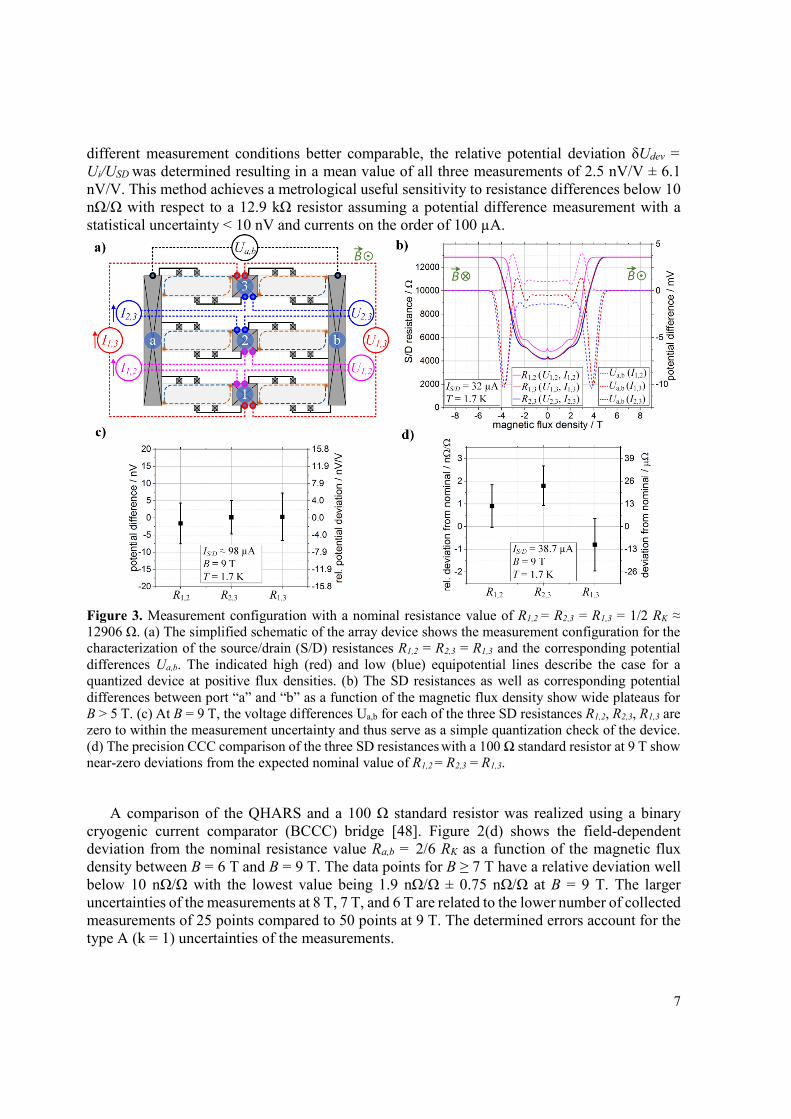
Figure 2. Measurement configuration with a nominal resistance value of Ra/b = 2/6 RK ≈ 8604 Ω. (a) The
simplified schematic of the array device shows the measurement configuration for the characterization
of the source/drain (SD) resistance of Ra/b = Ua,b/Ia,b and the potential differences U1,2, U2,3 and U1,3. The
indicated high (red) and low (blue) equipotential lines describe the case for a quantized device at positive
flux densities. (b) The SD resistance and the potential differences Ui at the center locations 1,2,3 as a
function of the magnetic flux density show wide plateaus for B > 5 T. (c) Measurements at B = 9 T show
that once resistance quantization is obtained, the voltage differences at the center locations 1,2,3 become
zero within the measurement uncertainty and thus serve as a simple quantization check of the device. (d)
The precision CCC comparison of Ra/b with a 100 Ω standard resistor for B = 9 T shows a deviation of ≈
2 nΩ/Ω from the expected nominal value.
7
different measurement conditions better comparable, the relative potential deviation δUdev =
Ui/USD was determined resulting in a mean value of all three measurements of 2.5 nV/V ± 6.1
nV/V. This method achieves a metrological useful sensitivity to resistance differences below 10
nΩ/Ω with respect to a 12.9 kΩ resistor assuming a potential difference measurement with a
statistical uncertainty < 10 nV and currents on the order of 100 µA.
A comparison of the QHARS and a 100 Ω standard resistor was realized using a binary
cryogenic current comparator (BCCC) bridge [48]. Figure 2(d) shows the field-dependent
deviation from the nominal resistance value Ra,b = 2/6 RK as a function of the magnetic flux
density between B = 6 T and B = 9 T. The data points for B ≥ 7 T have a relative deviation well
below 10 nΩ/Ω with the lowest value being 1.9 nΩ/Ω ± 0.75 nΩ/Ω at B = 9 T. The larger
uncertainties of the measurements at 8 T, 7 T, and 6 T are related to the lower number of collected
measurements of 25 points compared to 50 points at 9 T. The determined errors account for the
type A (k = 1) uncertainties of the measurements.
Figure 3. Measurement configuration with a nominal resistance value of R1,2 = R2,3 = R1,3 = 1/2 RK ≈
12906 Ω. (a) The simplified schematic of the array device shows the measurement configuration for the
characterization of the source/drain (S/D) resistances R1,2 = R2,3 = R1,3 and the corresponding potential
differences Ua,b. The indicated high (red) and low (blue) equipotential lines describe the case for a
quantized device at positive flux densities. (b) The SD resistances as well as corresponding potential
differences between port “a” and “b” as a function of the magnetic flux density show wide plateaus for
B > 5 T. (c) At B = 9 T, the voltage differences Ua,b for each of the three SD resistances R1,2, R2,3, R1,3 are
zero to within the measurement uncertainty and thus serve as a simple quantization check of the device.
(d) The precision CCC comparison of the three SD resistances with a 100 Ω standard resistor at 9 T show
near-zero deviations from the expected nominal value of R1,2 = R2,3 = R1,3.

8
3.2. Measurement configuration 2 results, R = 1/2 RK ≈ 12906 Ω
In the second measurement set shown in Figure 3(a), the QHARS device was contacted such
that only four out of the six devices contributed to the transport, creating a network with two
parallel pairs of series-connected devices. This was achieved by using the terminals “1,2,3” as
current terminals such that R1,2 = R2,3 = R1,3 with a nominal value of 1/2 RK ≈ 12906 Ω. The
terminals “a” and “b” were used to identify asymmetries in the device by monitoring the potential
difference Ua,b.
Figure 3(b) shows the field dependence of R1,2, R2,3 and R1,3 and their corresponding
potential differences Ua,b monitored with a lock-in measurement system within the range of
available magnetic flux densities of -9 T ≤ B ≤ 9 T. Small differences in the charge carrier
densities and low-field resistivities of the devices resulted in somewhat different onsets of the
resistance plateaus at 1/2 RK ≈ 12906 Ω around ±5 T. Measurements of Ua,b in Figure 3(b) show
that the potential differences of all three measurements with a mean value of -0.29 nV ± 4.7 nV
are zero to within the measurement uncertainty and thus indicate the well quantization of all Hall
elements.
The CCC resistance comparison of the QHARS against the same 100 Ω standard resistor in
Figure 3(c) proves that all three resistances R1,2, R2,3 and R1,3 were well quantized at 1/2 RK with
a deviation of ≈ ±2 nΩ/Ω.
4. Conclusions
We have demonstrated the fabrication and functionality of EG-based QHARS that provide
variable resistances with excellent quantization properties resulting in deviations from its
nominal value on the order of ± 2 nΩ/Ω. Additionally, the introduced relative potential deviation
measurements between points of equal potential in the symmetric network design were
successfully applied to verify the uniformity and quantization of the device. This technique does
not require the assessment of individual devices and thus represents a straightforward
quantization criterion of QHARS.
The reasons for the reported performance that matches that of single quantum Hall devices
are the crossover-free, superconducting NbTiN interconnections that eliminate ohmic resistance
contributions and Hall fluctuations as well as the applied split contacts with minimum contact
resistances. By presenting a novel way to simplify device interconnections without altering the
quantized resistance value this work brings the development of QHARS to the next stage.
Author Contributions
M.K. and A.F.R have contributed equally to this manuscript. M.K., A.F.R., and R.E.E.
developed the EG functionalization process. M.K., A.R.P., M.M., D.P., A.F.R., and H.J.
performed transport measurements. M.K. produced the graphene samples and fabricated the
devices. The manuscript was written through the contributions of all authors. All authors have
given approval to the final version of the manuscript.
Acknowledgments
The work of D.P. at NIST was made possible by arrangement with C.-T. Liang of National
Taiwan University, and the work of M.M. at NIST was made possible by arrangement with M.
Ortolano of Politecnico di Torino and L. Callegaro of the Istituto Nazionale di Ricerca

9
Metrologica, Turin, Italy. The authors would like to thank S. Schlamminger and A. Biacchi for
their assistance during the internal review at NIST. Commercial equipment, instruments, and
materials are identified in this paper in order to specify the experimental procedure adequately.
Such identification is not intended to imply recommendation or endorsement by the National
Institute of Standards and Technology or the United States government, nor is it intended to
imply that the materials or equipment identified are necessarily the best available for the purpose.
References
[1] Geim A K and Novoselov K S 2007 The rise of graphene Nat. Mater. 6 183–91 [2] Castro Neto A H, Guinea F, Peres N M R, Novoselov K S and Geim A K 2009 The
electronic properties of graphene Rev. Mod. Phys. 81 109–62 [3] Novoselov K S, Fal′ko V I, Colombo L, Gellert P R, Schwab M G and Kim K 2012
A roadmap for graphene Nature 490 192–200 [4] Das Sarma S, Adam S, Hwang E H and Rossi E 2011 Electronic transport in two-
dimensional graphene Rev. Mod. Phys. 83 407–70 [5] Berger C, Song Z, Li T, Li X, Ogbazghi A Y, Feng R, Dai Z, Alexei N, Conrad M E
H, First P N and De Heer W A 2004 Ultrathin epitaxial graphite: 2D electron gas properties and a route toward graphene-based nanoelectronics J. Phys. Chem. B 108 19912–6
[6] Virojanadara C, Syväjarvi M, Yakimova R, Johansson L I, Zakharov A A and Balasubramanian T 2008 Homogeneous large-area graphene layer growth on SiC(0001) Phys. Rev. B 78 245403
[7] Emtsev K V., Bostwick A, Horn K, Jobst J, Kellogg G L, Ley L, McChesney J L, Ohta T, Reshanov S A, Röhrl J, Rotenberg E, Schmid A K, Waldmann D, Weber H B and Seyller T 2009 Towards wafer-size graphene layers by atmospheric pressure graphitization of silicon carbide Nat. Mater. 8 203–7
[8] Kruskopf M, Pakdehi D M, Pierz K, Wundrack S, Stosch R, Dziomba T, Götz M, Baringhaus J, Aprojanz J, Tegenkamp C, Lidzba J, Seyller T, Hohls F, Ahlers F J and Schumacher H W 2016 Comeback of epitaxial graphene for electronics: large-area growth of bilayer-free graphene on SiC 2D Mater. 3 041002
[9] Kruskopf M and Elmquist R E 2018 Epitaxial graphene for quantum resistance metrology Metrologia 55 R27–36
[10] Janssen T J B M, Tzalenchuk A, Yakimova R, Kubatkin S, Lara-Avila S, Kopylov S and Fal’ko V I 2011 Anomalously strong pinning of the filling factor ν=2 in epitaxial graphene Phys. Rev. B 83 233402
[11] Ribeiro-Palau R, Lafont F, Brun-Picard J, Kazazis D, Michon A, Cheynis F, Couturaud O, Consejo C, Jouault B, Poirier W and Schopfer F 2015 Quantum Hall resistance standard in graphene devices under relaxed experimental conditions Nat. Nanotechnol. 10 965–71
[12] Tzalenchuk A, Lara-Avila S, Kalaboukhov A, Paolillo S, Syväjärvi M, Yakimova R, Kazakova O, Janssen T J B M, Fal’ko V and Kubatkin S 2010 Towards a quantum resistance standard based on epitaxial graphene Nat. Nanotechnol. 5 186–9
[13] Real M A, Lass E A, Liu F-H, Shen T, Jones G R, Soons J A, Newell D B, Davydov A V. and Elmquist R E 2013 Graphene Epitaxial Growth on SiC(0001) for Resistance Standards IEEE Trans. Instrum. Meas. 62 1454–60
[14] Lafont F, Ribeiro-Palau R, Kazazis D, Michon A, Couturaud O, Consejo C,

10
Chassagne T, Zielinski M, Portail M, Jouault B, Schopfer F and Poirier W 2015 Quantum hall resistance standards from graphene grown by chemical vapour deposition on silicon carbide Nat. Commun. 6 1–10
[15] Janssen T J B M, Rozhko S, Antonov I, Tzalenchuk A, Williams J M, Melhem Z, He H, Lara-Avila S, Kubatkin S and Yakimova R 2015 Operation of graphene quantum Hall resistance standard in a cryogen-free table-top system 2D Mater. 2 035015
[16] Jeckelmann B and Jeanneret B 2001 The quantum Hall effect as an electrical resistance standard Reports Prog. Phys. 64 1603–55
[17] Rigosi A F, Panna A R, Payagala S U, Kruskopf M, Kraft M E, Jones G R, Wu B-Y, Lee H-Y, Yang Y, Hu J, Jarrett D G, Newell D B and Elmquist R E 2019 Graphene Devices for Tabletop and High-Current Quantized Hall Resistance Standards IEEE Trans. Instrum. Meas. 68 1870–8
[18] Novikov S, Lebedeva N, Hämäläinen J, Iisakka I, Immonen P, Manninen A J and Satrapinski A 2016 Mini array of quantum Hall devices based on epitaxial graphene J. Appl. Phys. 119 174504
[19] Lartsev A, Lara-Avila S, Danilov A, Kubatkin S, Tzalenchuk A and Yakimova R 2015 A prototype of R K /200 quantum Hall array resistance standard on epitaxial graphene J. Appl. Phys. 118 044506
[20] Delahaye F 1993 Series and parallel connection of multiterminal quantum Hall‐effect devices J. Appl. Phys. 73 7914–20
[21] Delahaye F and Jeckelmann B 2003 Revised technical guidelines for reliable dc measurements of the quantized Hall resistance Metrologia 40 217–23
[22] Poirier W, Bounouh A, Piquemal F and André J P 2004 A new generation of QHARS: discussion about the technical criteria for quantization Metrologia 41 285–94
[23] Konemann J, Ahlers F-J, Pesel E, Pierz K and Schumacher H W 2011 Magnetic Field Reversible Serial Quantum Hall Arrays IEEE Trans. Instrum. Meas. 60 2512–6
[24] Jeffery A, Elmquist R E and Cage M E 1995 Precision tests of quantum hall effect device DC equivalent circuit using double-series and triple-series connections J. Res. Natl. Inst. Stand. Technol. 100 677
[25] Kruskopf M, Rigosi A F, Panna A R, Patel D K, Jin H, Marzano M, Berilla M, Newell D B and Elmquist R E 2019 Two-Terminal and Multi-Terminal Designs for Next-Generation Quantized Hall Resistance Standards: Contact Material and Geometry IEEE Trans. Electron Devices 1–5
[26] Büttiker M 1988 Absence of backscattering in the quantum Hall effect in multiprobe conductors Phys. Rev. B 38 9375–89
[27] Baker A M R, Alexander-Webber J A, Altebaeumer T, Janssen T J B M, Tzalenchuk A, Lara-Avila S, Kubatkin S, Yakimova R, Lin C-T, Li L-J and Nicholas R J 2012 Weak localization scattering lengths in epitaxial, and CVD graphene Phys. Rev. B 86 235441
[28] Drabińska A, Kamińska M, Wołoś A, Strupinski W, Wysmołek A, Bardyszewski W, Bożek R and Baranowski J M 2013 Enhancement of elastic and inelastic scattering lengths in quasi-free-standing graphene measured with contactless microwave spectroscopy Phys. Rev. B 88 165413
[29] Sahu M R, Liu X, Paul A K, Das S, Raychaudhuri P, Jain J K and Das A 2018 Inter-Landau-level Andreev Reflection at the Dirac Point in a Graphene Quantum

11
Hall State Coupled to a NbSe2 Superconductor Phys. Rev. Lett. 121 086809 [30] Amet F, Ke C T, Borzenets I V., Wang J, Watanabe K, Taniguchi T, Deacon R S,
Yamamoto M, Bomze Y, Tarucha S and Finkelstein G 2016 Supercurrent in the quantum Hall regime Science (80-. ). 352 966–9
[31] Rickhaus P, Weiss M, Marot L and Schönenberger C 2012 Quantum Hall Effect in Graphene with Superconducting Electrodes Nano Lett. 12 1942–5
[32] Hou Z, Xing Y, Guo A-M and Sun Q-F 2016 Crossed Andreev effects in two-dimensional quantum Hall systems Phys. Rev. B 94 064516
[33] Yang Y, Cheng G, Mende P, Calizo I G, Feenstra R M, Chuang C, Liu C-W, Liu C, Jones G R, Hight Walker A R and Elmquist R E 2017 Epitaxial graphene homogeneity and quantum Hall effect in millimeter-scale devices Carbon N. Y. 115 229–36
[34] Nagase M, Hibino H, Kagashima H and Yamaguchi H 2008 Local conductance measurement of few-layer graphene on SiC substrate using an integrated nanogap probe J. Phys. Conf. Ser. 100 052006
[35] Low T, Perebeinos V, Tersoff J and Avouris P 2012 Deformation and Scattering in Graphene over Substrate Steps Phys. Rev. Lett. 108 096601
[36] Willke P, Kotzott T, Pruschke T and Wenderoth M 2017 Magnetotransport on the nano scale Nat. Commun. 8 15283
[37] Momeni Pakdehi D, Aprojanz J, Sinterhauf A, Pierz K, Kruskopf M, Willke P, Baringhaus J, Stöckmann J P, Traeger G A, Hohls F, Tegenkamp C, Wenderoth M, Ahlers F J and Schumacher H W 2018 Minimum Resistance Anisotropy of Epitaxial Graphene on SiC ACS Appl. Mater. Interfaces 10
[38] Panchal V, Yang Y, Cheng G, Hu J, Kruskopf M, Liu C-I, Rigosi A F, Melios C, Hight Walker A R, Newell D B, Kazakova O and Elmquist R E 2018 Confocal laser scanning microscopy for rapid optical characterization of graphene Commun. Phys. 1 83
[39] Bekyarova E, Sarkar S, Niyogi S, Itkis M E and Haddon R C 2012 Advances in the chemical modification of epitaxial graphene J. Phys. D. Appl. Phys. 45 154009
[40] Che S, Jasuja K, Behura S K, Nguyen P, Sreeprasad T S and Berry V 2017 Retained Carrier-Mobility and Enhanced Plasmonic-Photovoltaics of Graphene via ring-centered η 6 Functionalization and Nanointerfacing Nano Lett. 17 4381–9
[41] Chen M, Pekker A, Li W, Itkis M E, Haddon R C and Bekyarova E 2018 Organometallic chemistry of graphene: Photochemical complexation of graphene with group 6 transition metals Carbon N. Y. 129 450–5
[42] Pinto H and Markevich A 2014 Electronic and electrochemical doping of graphene by surface adsorbates Beilstein J. Nanotechnol. 5 1842–8
[43] Chuang C, Yang Y, Pookpanratana S, Hacker C A, Liang C-T and Elmquist R E 2017 Chemical-doping-driven crossover from graphene to “ordinary metal” in epitaxial graphene grown on SiC Nanoscale 9 11537–44
[44] Rigosi A F, Kruskopf M, Hill H M, Jin H, Wu B-Y, Johnson P E, Zhang S, Berilla M, Hight Walker A R, Hacker C A, Newell D B and Elmquist R E 2019 Gateless and reversible Carrier density tunability in epitaxial graphene devices functionalized with chromium tricarbonyl Carbon N. Y. 142 468–74
[45] Breznay N P and Kapitulnik A 2013 Observation of the ghost critical field for superconducting fluctuations in a disordered TaN thin film Phys. Rev. B 88 104510
[46] Destraz D, Ilin K, Siegel M, Schilling A and Chang J 2017 Superconducting

12
fluctuations in a thin NbN film probed by the Hall effect Phys. Rev. B 95 1–6 [47] Hernandez-Marquez F L, Bierzychudek M E, Jones G R and Elmquist R E 2014
Precision high-value resistance scaling with a two-terminal cryogenic current comparator Rev. Sci. Instrum. 85 044701
[48] Götz M and Drung D 2017 Stability and Performance of the Binary Compensation Unit for Cryogenic Current Comparator Bridges IEEE Trans. Instrum. Meas. 66 1467–74
![Quantum many-body dynamics in optomechanical arrays€¦ · rays for quantum information processing [3, 4] have been proposed. Given these developments, one is led to ex-plore quantum](https://static.fdocuments.net/doc/165x107/5f0c77227e708231d43589e6/quantum-many-body-dynamics-in-optomechanical-rays-for-quantum-information-processing.jpg)


![Quantum Simulation Possibilities with 2-d Ion Arrays in a ...muellergroup.lassp.cornell.edu/aspen/Quantum... · 5/25/2009 · BT/(4πn oe2)]1/2 quadratic trap potential, eφ T ~](https://static.fdocuments.net/doc/165x107/5fd7a491ce2f41183f1ac1ae/quantum-simulation-possibilities-with-2-d-ion-arrays-in-a-5252009-bt4n.jpg)


![ORDERED ARRAYS OF QUANTUM DOTS: FORMATION ...in the formation of corrugated superlattices[4,12,18]. Another class of self-organized structures suitable for quantum wire and quantum](https://static.fdocuments.net/doc/165x107/60af1af733a8e8299668a051/ordered-arrays-of-quantum-dots-formation-in-the-formation-of-corrugated-superlattices41218.jpg)


