Modeling Ambipolar Behavior under High Current Injection ...
Approach:
OTFT Characterization: Interpretation:
Conclusion:
New unsymmetrical pentacene derivatives with ambipolar charge carrier transport for organic thin-film transistors
References: [1] J. E. Anthony, Angew. Chem. Int. Ed. 2008, 47, 452–483. [2] F. Würthner, R. Schmidt, ChemPhysChem. 2006, 7, 793–797. [3] C. R. Swartz, S. R. Parkin, J. E. Bullock, J. E. Anthony, A. C. Mayer, G. G. Malliaras, Org. Lett. 2005, 7, 3163– 3166. [4] D. Lehnherr, R. R. Tykwinski, Aust. J. Chem. 2011, 64, 919–929. [5] D. Lehnherr, A. H. Murray, R. McDonald, M. J. Ferguson, R. R. Tykwinski, Chem. Eur. J. 2009, 15, 12580– 12584. [6] M. J. S. Dewar, E. G. Zoebisch, E. F. Healy, J. J. P. Steward, J. Am. Chem. Soc. 1985, 107, 39023909; T. Clark, M. Hennemann, Erlangen 2011. [7] C. M. Jäger, T. Schmaltz, M. Novak, A. Khassanov, A. Vorobiev, M. Hennemann, A. Krause, H. Dietrich, D. Zahn, A. Hirsch, M. Halik, T. Clark, J. Am. Chem. Soc. 2013, 135, 4893–4900.
Acknowledgements:
Sebastian H. Etschela,b, Andreas R. Waterloob, Atefeh Y. Amina, Johannes T. Margrafc, Frank Hampelb, Christof Jägerc, Timothy Clarkc, Marcus Halika,* and Rik R. Tykwinskib,*
Motivation: Due to their versatile in functional groups, solubility in various solvents, and the resulting potential for low cost fabrication techniques, organic molecules with an extended π-conjugated backbone are of significant interest as semiconductors in organic electronic devices, like organic thin-film transistors (OTFTs).[1] Thereby, a close relationship between the solid state packing and the charge-carrier mobility has been observed.[2,3] Recently, synthetic routes for the synthesis of unsymmetrically substituted pentacene derivatives have been developped, in order to attach additional co-chromophores to a slouble pentacene π-system.[4,5] New unsymmetrical anthracenyl-pentacene derivatives have been obtained with orthogonal π-stacking of the two electronically decoupled acene sub-units, making them highly promising semiconductors for applications in OTFTs.
a Friedrich-Alexander Universität Erlangen-Nürnberg, Department of Chemistry and Pharmacy & Interdisciplinary Center of Molecular Materials (ICMM), Henkestraße 42, 91054 Erlangen, Germany. Fax: +49 9131 85 26865; Tel: +49 9131 85 22540; E-Mail: [email protected] b Friedrich-Alexander Universität Erlangen-Nürnberg, Institute of Polymer Materials, Organic Materials and Devices, Martenstraße 7, 91058 Erlangen, Germany. Fax: +49 9131 85 28321; Tel: +49 9131 85 27732; E-Mail: [email protected] c Friedrich-Alexander Universität Erlangen-Nürnberg, Computer Chemie Centrum, Nägelsbachstraße 25, 91052 Erlangen, Germany. Fax: +49 9131 85 26565; Tel: +49 9131 85 22948; E-Mail: [email protected]
Substrate
Semiconductor 1ac
Gate (Al)
AlOx Source (Au)
Drain (Au)
AlOx
1a
2D
1D 3.51 Å
3.61 Å
1c 1D 3.82 Å
1b 4.11 Å 3.32 Å
1D
Si
Si
Si
F
(Gate/Dielectric) [cm2/Vs]b,c,d (Gate/Dielectric) (Al/AlOx-C14PA)
Derivativea h (Si/SiO2)e h (Al/AlOx-
C14PA)f el (Al/AlOx-
C14PA)f Vth [V] Ion / Ioff
1a 1.210–7
2.010–8
1b 7.110–7
1.310–7
1.810–2
3.610–3 –1.85 (h+) 7.5102 (h+)
1c 6.810–7
3.210–7
1.610–1
2.910–2
7.610–3
1.810–3
–1.85 (h+) 2.61 (e–)
9.1104 (h+) 3.8103 (e–)
a vapor phase deposition of 1ac onto the according substrate; b OTFTs measured in the glove-box under N2; c mean value of at least three OTFTs; d W = 500 m; e L = 100 m; f L = 60 m.
-2,5 -2,0 -1,5 -1,0 -0,5 0,0
-8x10⁻⁸
-6x10⁻⁸
-4x10⁻⁸
-2x10⁻⁸
0
2x10⁻⁸
I D [
A]
VDS
[V]
VGS
= 0 V to -3.0 V
V =-0.5 V
-2 -1 0 1 2-1x10
-8
-5x10⁻⁹
0
5x10⁻⁹
1x10⁻⁸
VGS
= 0 V to 2.5 V
V =0.5 V
VGS
= 0 V to -2.5 V
V =-0.5 V
I D [
A]
VDS
[V]
OTFT with Al gate and AlOx-C14PA gate dielectric (compare Approach); W = 500 m, L = 60 m; Ion/Ioff = 1.5104, Ion/Ig = 1.2101, Vth = 1.6 V.
OTFT with Al gate and AlOx-C14PA gate dielectric (compare Approach); W = 500 m, L = 150 m; Ion/Ioff = 1.5104, Ion/Ig = 1.2101, Vth = 1.6 V.
-2 -1 1 2
0
1x10⁻⁴
2x10⁻⁴
3x10⁻⁴
el
= 0.03 cm2/Vs
VDS
= 2 V
VDS
= -2 V
I G [
A]
I
D [
A]
VGS
[V]
ÖI D
[ÖA
]
h = 0.1 cm
2/Vs
1c
10-13
10-12
10-11
10-10
10-9
10-8
10-7
10-6
-2,5 -2,0 -1,5 -1,0 -0,5 0,0 0,5
0
1x10⁻⁴
2x10⁻⁴
3x10⁻⁴
4x10⁻⁴
1b
I G [
A]
I
D [
A]
VDS
= -2V
VGS
[V]
ÖI D
[ÖA
]
10-13
10-12
10-11
10-10
10-9
10-8
10-7
10-6
h = 0,01 cm
2/Vs
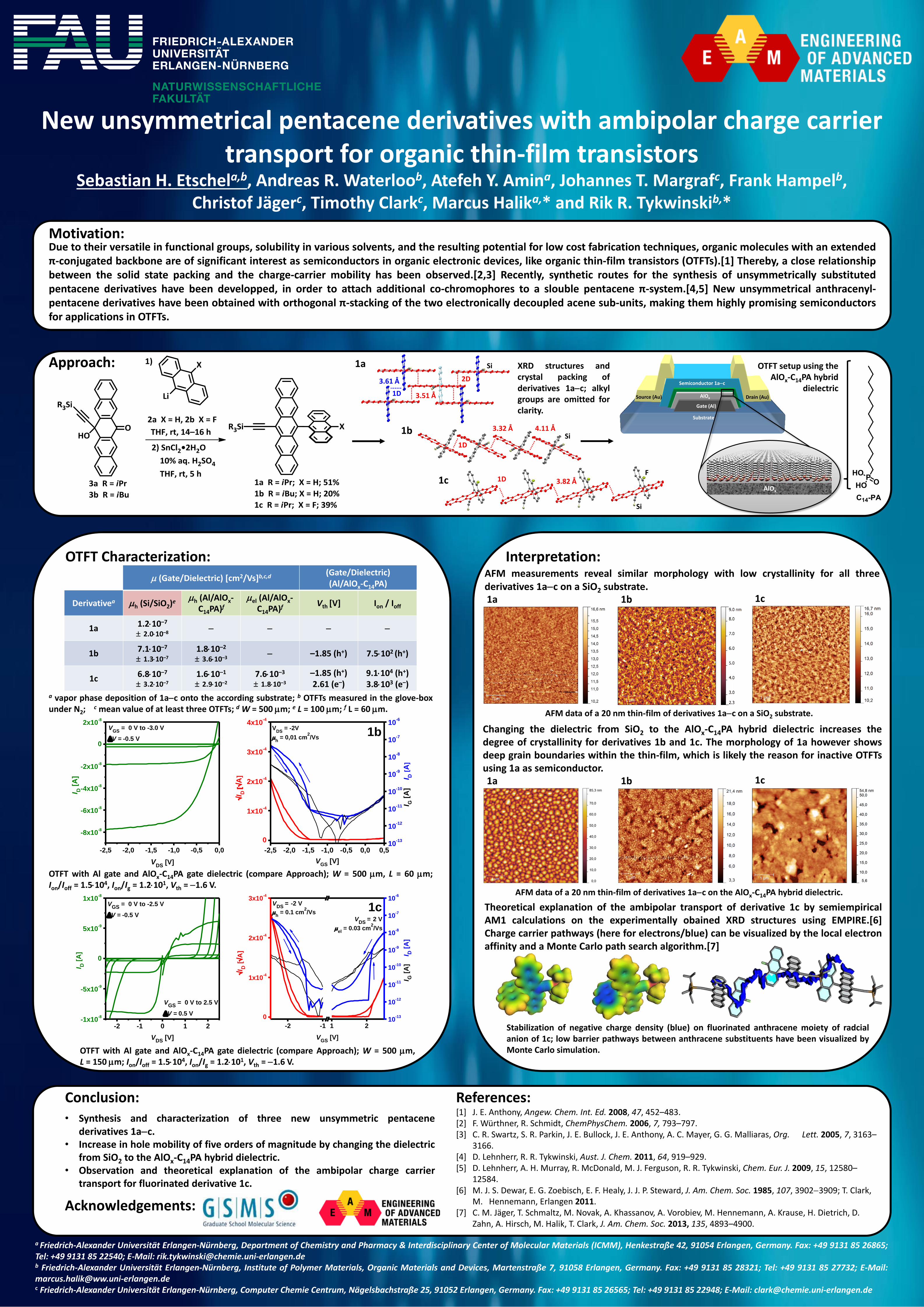
AFM measurements reveal similar morphology with low crystallinity for all three derivatives 1ac on a SiO2 substrate.
AFM data of a 20 nm thin-film of derivatives 1ac on a SiO2 substrate.
1a 1b 1c
Changing the dielectric from SiO2 to the AlOx-C14PA hybrid dielectric increases the degree of crystallinity for derivatives 1b and 1c. The morphology of 1a however shows deep grain boundaries within the thin-film, which is likely the reason for inactive OTFTs using 1a as semiconductor. 1a 1b 1c
AFM data of a 20 nm thin-film of derivatives 1ac on the AlOx-C14PA hybrid dielectric.
XRD structures and crystal packing of derivatives 1ac; alkyl groups are omitted for clarity.
• Synthesis and characterization of three new unsymmetric pentacene derivatives 1ac.
• Increase in hole mobility of five orders of magnitude by changing the dielectric from SiO2 to the AlOx-C14PA hybrid dielectric.
• Observation and theoretical explanation of the ambipolar charge carrier transport for fluorinated derivative 1c.
Theoretical explanation of the ambipolar transport of derivative 1c by semiempirical AM1 calculations on the experimentally obained XRD structures using EMPIRE.[6] Charge carrier pathways (here for electrons/blue) can be visualized by the local electron affinity and a Monte Carlo path search algorithm.[7]
Stabilization of negative charge density (blue) on fluorinated anthracene moiety of radcial anion of 1c; low barrier pathways between anthracene substituents have been visualized by Monte Carlo simulation.
OTFT setup using the AlOx-C14PA hybrid
dielectric