
New Materials and Novel Applications for CMP - Entrepix · Semiconductor Equipment Spare Parts and...
27
Semiconductor Equipment Spare Parts and Service CMP Foundry New Materials and Novel Applications for CMP Robert L. Rhoades, Ph.D. ICPT 2014 Kobe, Japan Nov 19-21, 2014
Transcript of New Materials and Novel Applications for CMP - Entrepix · Semiconductor Equipment Spare Parts and...

Semiconductor Equipment Spare Parts and Service CMP Foundry Semiconductor Equipment Spare Parts and Service CMP Foundry
New Materials and Novel Applications for CMP Robert L. Rhoades, Ph.D.
ICPT 2014
Kobe, Japan
Nov 19-21, 2014
Click to edit Master title style
2 11/24/2014
Outline
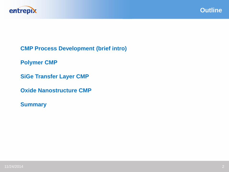
CMP Process Development (brief intro)
Polymer CMP
SiGe Transfer Layer CMP
Oxide Nanostructure CMP
Summary

Click to edit Master title style
3
Device Development Sequence
Materials Selection
Integration Planning
Process Development
Device Prototype
Optimization
Qualification
Pilot Production
High Volume Manufacturing
Development Sequence
Design Concept
• The vast majority of device development projects follow this basic path
• Each stage has certain inputs required, activities to be performed, and desired outputs that increase in difficulty and complexity for each successive stage
• Each stage assumes successful completion of the previous stage, or at least overlapping execution of the previous stage
• Failure at any stage usually means backing up at least one stage to try again
Click to edit Master title style
4
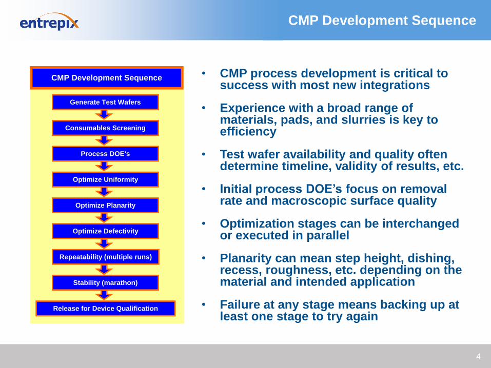
CMP Development Sequence
• CMP process development is critical to success with most new integrations
• Experience with a broad range of materials, pads, and slurries is key to efficiency
• Test wafer availability and quality often determine timeline, validity of results, etc.
• Initial process DOE’s focus on removal rate and macroscopic surface quality
• Optimization stages can be interchanged or executed in parallel
• Planarity can mean step height, dishing, recess, roughness, etc. depending on the material and intended application
• Failure at any stage means backing up at least one stage to try again
Consumables Screening
Process DOE's
Optimize Uniformity
Optimize Planarity
Optimize Defectivity
Stability (marathon)
Release for Device Qualification
CMP Development Sequence
Generate Test Wafers
Repeatability (multiple runs)
Click to edit Master title style
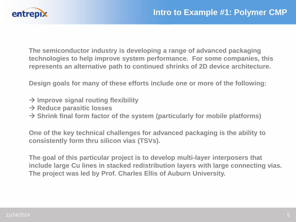
The semiconductor industry is developing a range of advanced packaging
technologies to help improve system performance. For some companies, this
represents an alternative path to continued shrinks of 2D device architecture.
Design goals for many of these efforts include one or more of the following:
Improve signal routing flexibility
Reduce parasitic losses
Shrink final form factor of the system (particularly for mobile platforms)
One of the key technical challenges for advanced packaging is the ability to
consistently form thru silicon vias (TSVs).
The goal of this particular project is to develop multi-layer interposers that
include large Cu lines in stacked redistribution layers with large connecting vias.
The project was led by Prof. Charles Ellis of Auburn University.
11/24/2014 5
Intro to Example #1: Polymer CMP

Click to edit Master title style
11/24/2014 6
Dielectric Choice
From 3 potentially viable alternatives, ALX2010 was chosen
Click to edit Master title style
11/24/2014 7
Fabrication Sequence (part 1)
Silicon
Silicon Dioxide
Seed Layer
Photoresist
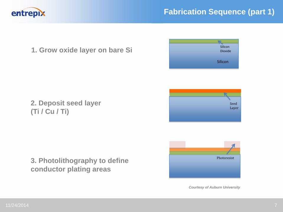
1. Grow oxide layer on bare Si
2. Deposit seed layer
(Ti / Cu / Ti)
3. Photolithography to define
conductor plating areas
Courtesy of Auburn University
Click to edit Master title style
11/24/2014 8
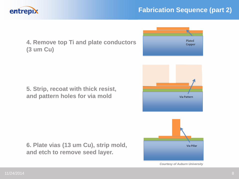
Fabrication Sequence (part 2)
Via Pattern
Plated Copper
Via Pillar
4. Remove top Ti and plate conductors
(3 um Cu)
5. Strip, recoat with thick resist,
and pattern holes for via mold
6. Plate vias (13 um Cu), strip mold,
and etch to remove seed layer.
Courtesy of Auburn University

Click to edit Master title style
11/24/2014 9
Fabrication Sequence (part 3)
AL-X2010
7. Deposit ALX to a thickness slightly
thicker (2-3 um) than via height
8. CMP to planarize ALX and expose
tops of Cu vias
Courtesy of Auburn University
Click to edit Master title style
11/24/2014 10
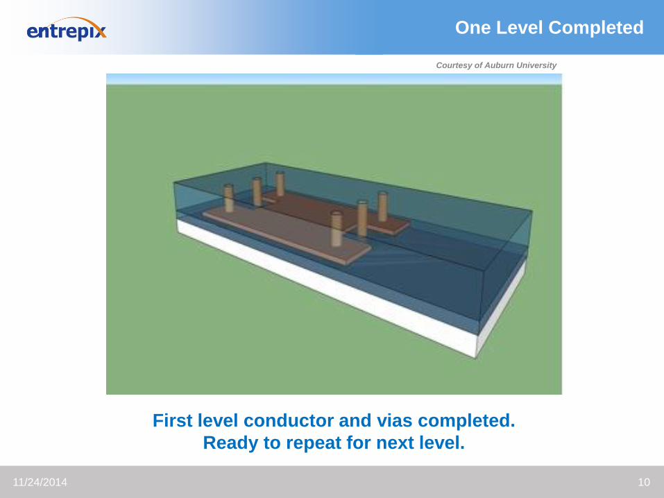
One Level Completed
First level conductor and vias completed.
Ready to repeat for next level.
Courtesy of Auburn University
Click to edit Master title style
SCREENING EXPERIMENTS
Started with assortment of
proven slurries used with
other materials
Same type of pad was used
for all trials, but new pad
installed for major changes in
particle type
Most slurries suffered one or
both of 2 primary failure
modes:
1) low removal rate and/or
2) severe scratching
Slurry with best performance
on the ALX2010 in this test
was a colloidal alumina
Process summary at right
11/24/2014 11
CMP Development
CMP Process SummaryWafer size 100mm
Material Polymer ALX2010
INPUTS
PlatformIPEC 472
(later transferred to other platforms)
Primary Pad IC1000 k-groove on SubaIV
Primary Slurry colloidal alumina
Final Pad Politex embossed
Final Slurry or Chemistry None
Pad Conditioning 3M (4.25" standard)
Downforce 5 psi
Back Pressure 1 psi
Platen Speed 30 rpm
Carrier Speed 37 rpm
Slurry Flow 100 ml/min
CMP RESULTS
Polymer Removal Rate 6000 - 7500 Ang/min
PlanarizationVery good for this application
Minimal dishing on Cu posts once exposed
Polymer surface finish Excellent with no scratching
Cu surface finish Good with no major scratching or pitting

Click to edit Master title style
11/24/2014 12
Planarization Efficiency
Pre-CMP
S.H. ~ 12.5 mm
Post-CMP
S.H. ~ 0.35 mm
Planarization efficiency of roughly 97%
Click to edit Master title style
11/24/2014 13
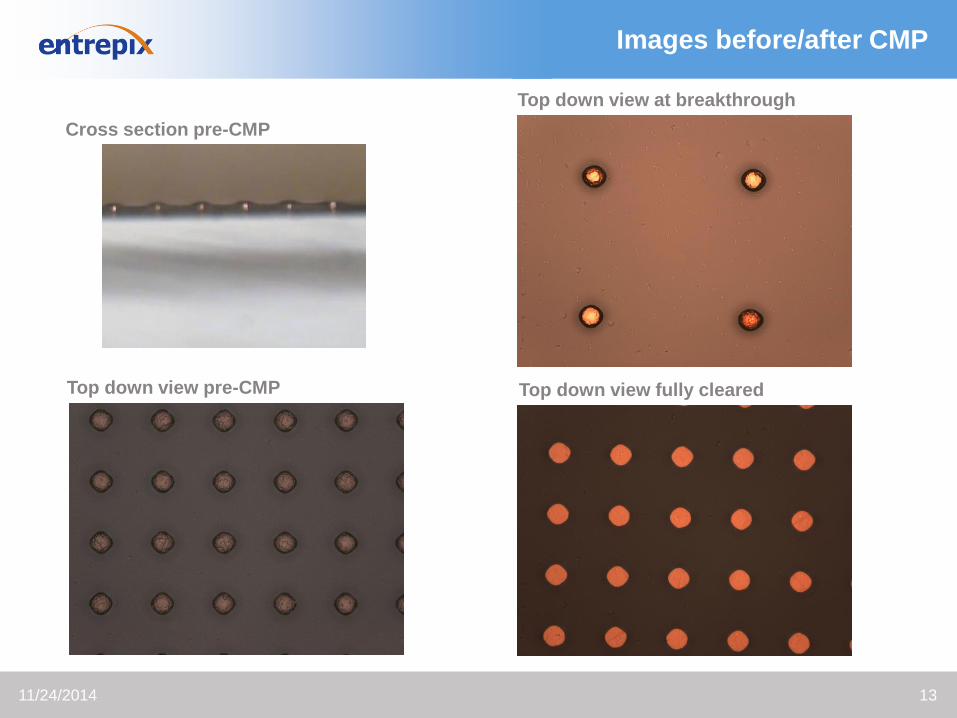
Images before/after CMP
Cross section pre-CMP
Top down view pre-CMP
Top down view at breakthrough
Top down view fully cleared

Click to edit Master title style
11/24/2014 14
Top down view and xsection SEM
Buried conductor (thru polymer)
and via posts with tops
cleared after CMP
Cross section SEM of
finished interposer with
3 levels of metal.
Courtesy of Auburn University
Click to edit Master title style
Filled (solid) Cu vias which have low resistance and are large enough to
carry substantial current
No need to pattern dielectric
(can utilize any dielectric that can be polished)
High aspect ratio capability – depends on photoresist aspect ratio
Very good planarization – easy to add multiple signal layers
11/24/2014 15
Advantages of Chosen Process Flow

Click to edit Master title style
11/24/2014 16
Device pic #1
Courtesy of Auburn University
Click to edit Master title style
11/24/2014 17
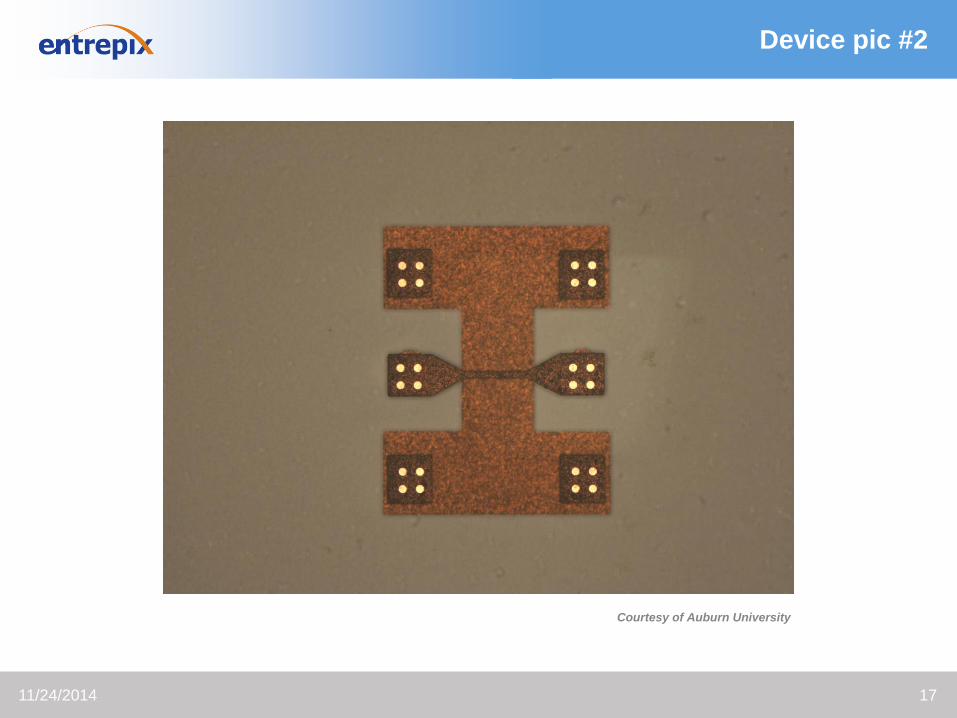
Device pic #2
Courtesy of Auburn University

Click to edit Master title style
SiGe transferred from a donor substrate to an oxide layer on a Si wafer
(similar to Smart-Cut SOI technique). Surface of SiGe after splitting is
slightly rougher than desired.
Process targets:
Reduce roughness of transferred SiGe layer to less than 5 Ang
Minimize amount of material removed to achieve above
Minimize all sources of added thickness variation
Most previous SiGe polishing processes removed too much material, or
induced too much thickness variation, even when used for relatively
short polish times. Success for this project required that a customized
process be developed.
11/24/2014 18
Intro to Example #2: SiGe Transfer Layer

Click to edit Master title style
19
SOI Smart-Cut Flow
• Developed at CEA-Leti
• Six key steps
– Oxidation
– Hydrogen implantation
– Direct wafer bonding
– Splitting
– Annealing
– Touch or “Kiss” polishing
• Very flexible for thickness of buried
oxide & top Si layers
• H+ damage relatively easy to anneal
Source: “SOI Technology” by Vishwas Jaju, 2004

Click to edit Master title style
20
SiGe Polish Rate vs Composition
SiGe polish rate
is a strong non-
linear function of
composition
below 30% Ge.
This project was
focused around
50% Ge layers,
so rate was
insensitive to
small changes in
composition.
Click to edit Master title style
21
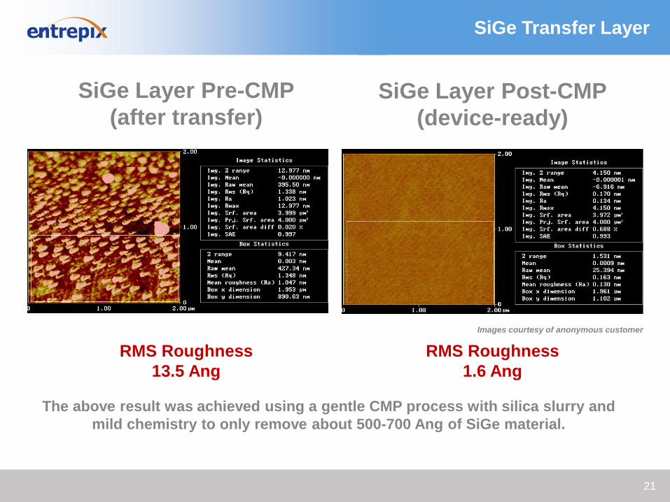
SiGe Transfer Layer
SiGe Layer Pre-CMP
(after transfer)
SiGe Layer Post-CMP
(device-ready)
RMS Roughness
13.5 Ang
RMS Roughness
1.6 Ang
The above result was achieved using a gentle CMP process with silica slurry and
mild chemistry to only remove about 500-700 Ang of SiGe material.
Images courtesy of anonymous customer

Click to edit Master title style
This project involves extremely repetitive inlaid nanostructures. After
etching, recessed features of ~100nm depth are filled with densified CVD
oxide then planarized using CMP.
Process targets:
Clear oxide over field areas as uniformly as possible
Minimize Si loss after breakthrough
Minimize topography after CMP to <1 nm if possible
CMP process approach:
- High selectivity STI slurry (ceria based)
- Standard planarizing pad
- Gentle conditioning
- Non-aggressive polishing recipe (about 2.5-3 psi and 70-90 rpm)
11/24/2014 22
Intro to Example #3: Oxide nanostructures
Click to edit Master title style
23
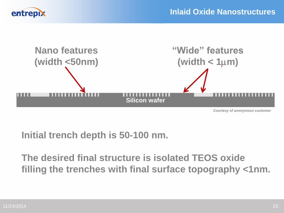
Inlaid Oxide Nanostructures
11/24/2014
Silicon wafer
Nano features
(width <50nm)
“Wide” features
(width < 1mm)
Initial trench depth is 50-100 nm.
The desired final structure is isolated TEOS oxide
filling the trenches with final surface topography <1nm.
Courtesy of anonymous customer

Click to edit Master title style
24
Post-CMP Topography <1nm
Slot 18: 105S POLISH
Slot 23:
120S POLISH
Wafer Center Wafer Edge
Images courtesy of anonymous customer
Click to edit Master title style
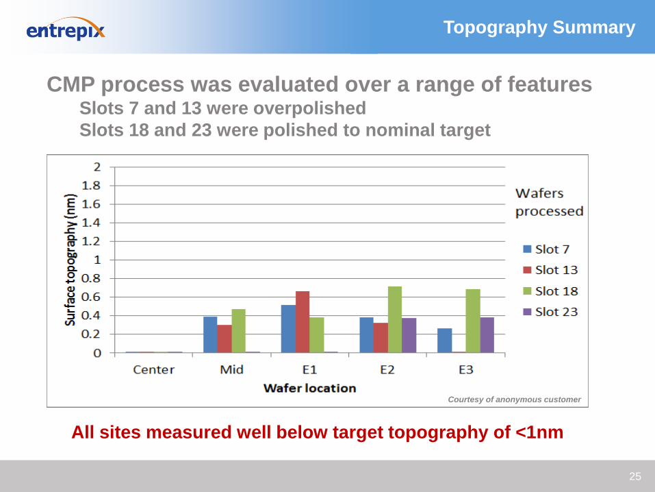
25
Topography Summary
CMP process was evaluated over a range of features Slots 7 and 13 were overpolished
Slots 18 and 23 were polished to nominal target
All sites measured well below target topography of <1nm
Courtesy of anonymous customer
Click to edit Master title style
CMP development is more efficient when approached systematically.
Polymer CMP
Targeted at a novel integration for multi-layer interposer
Required initial screening of slurries … colloidal alumina chosen
Achieved good surface finish and reasonable RR >0.5um/min
SiGe Transfer Layer CMP
Similar to Smart-Cut SOI fabrication sequence
Achieved RMS roughness <2 Ang with 500-700 Ang CMP removal
Oxide Nanostructure CMP
Planarization of very small oxide-filled trenches (50-100nm deep)
Minimal Si loss after clearing in field regions required using ceria
slurry with high selectivity to Si
Final topography of <1nm achieved across 300mm wafers
11/24/2014 26
Summary
Click to edit Master title style Acknowledgements
Many thanks to the following:
• Terry Pfau, Paul Lenkersdorfer, Donna Grannis & Scott Drews of Entrepix
• Prof. Charles Ellis of Auburn University
• Anonymous customers who gave permission to use images and data
For additional information, please contact:
Robert L. Rhoades
Entrepix, Inc.
Chief Technology Officer
+1.602.426.8668
27