NEPP ETW 2011: Class Y: NEPP Championed Approach to Advanced Package ... · PDF fileNEPP...
51
Presented at the NEPP Electronics Technology Workshop (ETW), NASA-GSFC www.nasa.gov National Aeronautics and Space Administration Class Y: NEPP Championed Approach to Advanced Package Qualification June 28, 2011 Shri Agarwal NASA Jet Propulsion Laboratory, California Institute of Technology [email protected] © 2011 California Institute of Technology. Government sponsorship acknowledged.
Transcript of NEPP ETW 2011: Class Y: NEPP Championed Approach to Advanced Package ... · PDF fileNEPP...

Presented at the NEPP Electronics Technology Workshop (ETW), NASA-GSFC
www.nasa.gov
National Aeronautics and Space Administration
Class Y:
NEPP Championed Approach
to
Advanced Package Qualification
June 28, 2011
Shri AgarwalNASA Jet Propulsion Laboratory, California Institute of Technology
© 2011 California Institute of Technology. Government sponsorship acknowledged.

2
Agenda• Progress so far• Background• Group Interactions
• Why “Class Y”?
• G12 Class Y Task Group Current Status• Road to QML-Y flight parts procurement• Summary
Attachments: Section 1:
Section 2:
Section 3:
Section 4:
MIL-PRF-38535, Rev J, Appendix B marked up for Class Y
MIL-STD-883, Rev H, and MIL-PRF-38535, Rev J
Developing Packaging for Class Y (credit: Mike Sampson)
Other Information
Launched June 10, 2011, the Aquarius/SAC-D mission is a partnership between NASA and Argentina’s
space agency, Comisión Nacional de Actividades Espaciales (CONAE) that will use advanced technologies to
make NASA’s first space-based measurements of ocean salinity across the globe.

3
BackgroundBack in 2009, there was a big push to bring the Xilinx Viirtex-4 (a non-hermetic part) into
the QML system as Class V device. NASA was not in favor as it would have created a
massive confusion. Mike Sampson conceived the idea of a new Class Y for non-hermetic
space parts to provide QML coverage for Xilinx Virtex-4 and similar devices.
A new G-12 Task Group, TG 2010-01, was formed in early 2010 to address non-hermetic
devices for space. Shri Agarwal was asked to lead the effort.
This task was challenging because it:
• Was far more involved than typical G12 tasks,
• Required development of a brand new concept,
• Used system-on-a-chip — one of the most complicated devices,
• Needed to be simple and easily understood,
• Possessed sketchy testing and board assembly boundaries, and
• Was needed to procure a standard QML product as quickly as possible.
Progress so farMajor milestone last month:
G12 approved DLA-VA’s kickoff of an
Engineering Practice (EP) Study for Class Y.
Launching in late 2014, SMAP (Soil Moisture Active Passive) will use a combined
radiometer and high-resolution radar to measure surface soil moisture and freeze-
thaw state, providing new opportunities for scientific advances and societal benefits.

4
G12
Class Y
Task Group
Manufacturers OEMs Others
Review
M. Sampson
Idea
Class Y
Concept
Development
EP Study
(DLA-VA)
Manufacturer Certification
to QML-Y (DLA-VQ) Solder
Terminations
Newly formed JC13 Task Groups with Class Y Interest
Burn-in,
electricals,
deltas
Use of
passives in
IC packages
Task Group Activities
Task Group Inputs
Government
G12 Class Y Task Group Interactions at a Glance
5
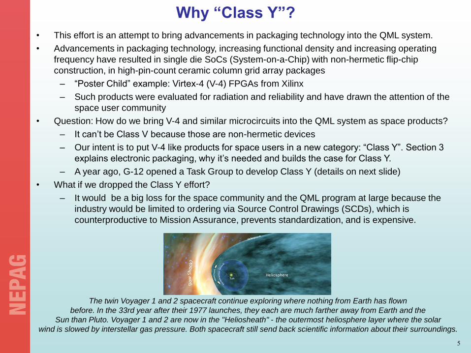
Why “Class Y”?
• This effort is an attempt to bring advancements in packaging technology into the QML system.
• Advancements in packaging technology, increasing functional density and increasing operating
frequency have resulted in single die SoCs (System-on-a-Chip) with non-hermetic flip-chip
construction, in high-pin-count ceramic column grid array packages
– ―Poster Child‖ example: Virtex-4 (V-4) FPGAs from Xilinx
– Such products were evaluated for radiation and reliability and have drawn the attention of the
space user community
• Question: How do we bring V-4 and similar microcircuits into the QML system as space products?
– It can’t be Class V because those are non-hermetic devices
– Our intent is to put V-4 like products for space users in a new category: ―Class Y‖. Section 3
explains electronic packaging, why it’s needed and builds the case for Class Y.
– A year ago, G-12 opened a Task Group to develop Class Y (details on next slide)
• What if we dropped the Class Y effort?
– It would be a big loss for the space community and the QML program at large because the
industry would be limited to ordering via Source Control Drawings (SCDs), which is
counterproductive to Mission Assurance, prevents standardization, and is expensive.
The twin Voyager 1 and 2 spacecraft continue exploring where nothing from Earth has flown
before. In the 33rd year after their 1977 launches, they each are much farther away from Earth and the
Sun than Pluto. Voyager 1 and 2 are now in the "Heliosheath" - the outermost heliosphere layer where the solar
wind is slowed by interstellar gas pressure. Both spacecraft still send back scientific information about their surroundings.

6
G12 Class Y Task Group Current Status
• G-12 Task Group formed in Jan.’10 to develop screening/qualification requirements for
non-hermetics for Space (TG2010-01).
• The TG’s 4 meetings may be summarized as follows:
– Average attendance ~ 80
– As soon as the TG was formed, users were enthusiastic and eager to know when they
could procure QML-Y flight parts? See slide 11 on road to procurement.
– A questionnaire was sent to a targeted group of users, manufacturers and others
(There are about 150 names on the Class Y distribution list). The major inputs were:
Class Y should cover those items that are ceramic flip-chip non-hermetic
construction that have passed the requirements of Appendix B. The broader issue
of organic based substrates would be addressed in the next phase of this work.
See slide 10 for the TG charter statement.
Some respondents asked why should space community even allow use of non-
hermetic parts. (Although the feasibility of a hermetic ceramic package with
under-fill flip-chip die has been demonstrated, there are sealing process, board
level, and other concerns. There are no current development programs as there
is no user interest.)
Add the word ―hermetic‖ to the definitions of QML-Q and QML-V classes in
38535.
NASA does not endorse attaching the description ―near hermetic‖ to Class Y.
(How do you quantify ―near-hermetic‖: it could be 10% or 99% hermetic, or less
than half, or…?). Both DLA-VA and DLA–VQ support NASA position.

7
G12 Class Y Task Group Current Status (Contd.)
• TG meetings summary (cont’d):
– Boeing proposed ―simplified approach‖ was adopted:
Add paragraph to existing 38535 Appendix B (labeled as Section 1) stating
differences for class Y (most remains same as Class V) – see Section 1 attached.
One key element in Section 1 is for the manufacturers to submit a Packaging
Integration Demonstration Test Plan (PIDTP) to QA for approval. This plan must
address issues unique to non-hermetic construction and materials, such as
potential materials degradation, interconnect reliability, thermal management,
resistance to processing stresses, thermo-mechanical stresses, shelf life, etc. The
PIDTP plan shall be approved by QA after consultation with the space community.
Separate issues related to non-hermeticity from those related to solder
terminations (see below).
Provide markups to other affected documents – see Section 2 attached.
– 8 manufacturers have so far expressed interest in offering Class Y products (Xilinx,
Actel, Intersil, Aeroflex, BAE, Honeywell, TI, e2v).
– Government customers and contractors have provided statements of support.
– Class Y defined as items that are of ceramic, non-hermetic construction.
– DLA Land and Maritime – VA (M. Akbar) was added to the team.
– Comment from G12 management: The group may be surprised at how quickly this is
moving. Most of the time, documents take over a year to get a full draft. You are far
ahead of schedule. People just may not realize that this is out of the conceptual stage
and into the writing stage.

8
G12 Class Y Task Group Current Status (Contd.)
─ Solder terminated parts (could be hermetic or non-hermetic) need attention.
Proposed a paragraph to add to MIL-PRF-38535, Appendix B (also part of Section
1). The JC-13.2 Task Group on solder terminations has been formed. The broad
issues are: solderability, storage and shelf life, electrical testing, reworks, pull test,
termination definition (Tin lead solder based?), etc. Some specific questions are:
What is the shelf life of the of the CGA? Specifically, how long will these
parts be 100% solderable? Is this guaranteed?
As the columns would tend to oxidize when exposed to atmosphere, how do
you store them: keep in sealed dry bags? Store in dry nitrogen?
Do all internal and external portions of the flip-chip package pass MIL-STD-
883, Method 5011 (re. evaluation of polymeric materials)?
Once assembled, can the finished CGA (Like all other microcircuits,
transistors, and hybrids) be functionally tested at -55C, 25C, and +125C? (If
the solder melting point is estimated at about 180C, then it would be risky to
electrically test the parts at 125C case temperature. Any cold brittle concerns
at -55C?)
What board/assembly level test have been run for temp cycling/vibration, etc
What is the max number of allowable column reworks for space products?
Specify column pull test
Inspection of CGAs (area arrays, in general)
Need application notes on CGAs after column attach so that the users know
what they are getting, any temperature limitations, adequacy of visual
inspection, cleanliness, fluxes to avoid, etc.
Coordination with IPC – what are the boundaries that separate JEDEC work
from IPC?

9
G12 Class Y Task Group Current Status (Contd.)
– Clarification needed on burn-in, electricals and delta requirements. This is a big issue for all
microcircuits and would apply to Class Y products as well. For instance, statements such
as, the V-4 has undergone 4000 hours of life test with parts biased in a static condition,
make you wonder why an FPGA which is basically a digital part was not subjected to a
dynamic condition? There are other questions related to the activation energy, low
temperature burn-in, etc. At the request of L. Harzstark and S. Agarwal, a JC13 Task Group
has been formed to clarify/update requirements in MIL-STD-883, Method 5004.
– The screening/qual requirements for signal conditioning capacitors should be clearly stated
– ref. MIL-PRF-38535, Paras 3.15 and 3.15.1. What is the attached method of the BME
capacitors used in many designs? During the G12 we heard couple of companies say they
use epoxy or silver glass die attachment material to adhere the capacitor to the internal
portion of the IC package. There are others who only use solder attachment. A JC13 Task
Group has been formed to address these issues.
─ What is a space flight part?
Land Grid Array, LGA, configuration (yes)
Column Grid Array, CGA, configuration (debatable)
– Will the set of 38535 classes, with Class Y added, cover microcircuits
for the next several years? (yes, per the poll taken of major manufacturers)
The NASA/ESA/ASI Cassini-Huygens mission has directly sampled the water plumes jetting
into space from Saturn’s moon Enceladus. The findings from these fly-thrus are the strongest
evidence yet for the existence of large-scale saltwater reservoirs beneath the moon’s icy crust.

10
G12 Class Y Task Group Current Status (Contd.)
– The Team requested G12 approval for DLA Land and Maritime - VA to conduct
an Engineering Practice (EP) study using the detailed requirement input the
Task Group has developed (Sections 1 & 2 attached). This request was
approved by G12.
– The Team’s request for clear approval of Task Group charter was also
approved by G12. The charter statement reads:
"This task group will develop requirements, including qualification and screening
standards, for non-hermetic, ceramic-based microcircuits suitable for space
applications. Initial effort will be focused on support for devices using flip-chip
ceramic column grid array packaging, with resulting requirements to be
submitted as a proposal for consideration to DLA Land and Maritime.―
NuSTAR (Nuclear Spectroscopic Telescope Array) will be the first focusing high
energy X-ray mission, opening up the hard X-ray sky for sensitive study. NuSTAR will
search for black holes, map supernova explosions, and study the most extreme active galaxies.

11
Road to QML-Y Flight Parts Procurement
• Major Milestones:
G12 approval of TG charter
G-12 Class Y Task Group to develop requirements
G12 approval for DLA-VA to commence EP study
DLA-VA to Conduct EP study and the Class Y Team to resolve issues
DLA-VA to add Class Y requirements into 38535 and 883
DLA-VQ to audit suppliers to Class Y requirements
– Users to procure QML-Y flight parts from certified suppliers
Gravity Recovery and Interior Laboratory (GRAIL) mission, using twin spacecraft flying in formation to investigate
the moon’s gravity field, a possible inner core and how Earth and other rocky planets formed, launches in late 2011.

Team resources include:
– Mike Sampson, NASA/GSFC
– Mark Porter, G12
– Brent Rhoton, JC13
– Anduin Touw, G12
– Mike Adams, DLA-VQ
– Rob Heber, DLA-VA
– Tom Hess, DLA-VA
– Charles Saffle, DLA-VA
The Team
12
The Team members are:
– Muhammad Akbar, DLA-VA
– Larry Harzstark, Aerospace
– David Sunderland, Boeing
– Shri Agarwal, NASA/JPL
– Tom Wilson, NASA/JPL
Launching in August 2011, the solar-powered Juno spacecraft enters a low, elliptical orbit circling
Jupiter from pole to pole to investigate secrets hidden beneath the planet's thick, colorful clouds. The innovative
orbit will avoid lethal belts of charged particles surrounding Jupiter like the less dense Van Allen belts encircling Earth.

• Military standards for microcircuits haven’t kept pace with developments in
packaging technology
• RADC (Rome Air Development Center) used to be the technical arm of DLA
(Defense Logistic Agency) and they did necessary evaluations to keep up with
new developments.
• NEPAG (NASA EEE Parts Assurance Group), which is like a large component
engineering group representing the government, is addressing some of the issues:
• 38535 Appendix H, new technology evaluation, update (L. Harzstark).
• Requirement for screening of passive elements was added to 38535.
• An out-of-box approach, Class Y, taken for non-hermetic parts (M. Sampson)
• Support to Counterfeit, PEMs and other JC13/G12 efforts
• Supporting new JC13 Task Groups: passives, solder term., screening.
• Support to 13.4: power MOSFETs, other (K. LaBel)
Some NEPAG Activities:
• Weekly Telecons
• Supplier Audits
• DLA Land & Maritime SMD reviews
• Others
NEPAG Contribution to MIL-STD
13

14
In Summary..
• G12 approval for DLA-VA to kick-off an EP study on Class Y marked the completion of a
major milestone for the Class Y initiative.
• During the Class Y meetings issues came up and the G12 and JC13 participants and
their managements were very helpful suggesting we appoint 3 additional JC13
committees to address them. Their support is appreciated.
• Progress reports will be made in future meetings. The work is ongoing and far from over.
• NEPP is making every effort to strengthen the MIL system and thereby support the flight
projects
– Thank you!
NASA's Mars Science Laboratory Curiosity rover, a mobile robot for investigating Mars' past or present
ability to sustain microbial life, is being tested in preparation for launch this fall.

15
Section 1
MIL-PRF-38535, Rev JAppendix B marked up for Class Y

16
Proposed Additions to Appendix B
B.5 Non-Hermetic Space Level Microcircuits – Class Y. This section presents the
requirements that are to be used to supplement this specification for non-hermetic
ceramic based space level microcircuits, hereinafter referred to as Class Y.
Requirements for Class Y products with solder terminations e.g. ball grid array (BGA) or
column grid array (CGA) packages, are covered under Para B.6 herein. Class Y
microcircuits must obey all previous provisions of Appendix B, except as follows:
B.5.1 Part of identifying number (PIN). Each Y level QML microcircuit shall be marked
with the device Class designator ―Y‖ in place of the ―V‖ designator in the PIN format, see
3.6.2a in the main body of this document.
B.5.2 Class Y Assembly Material: For flip chip assembly, solder bump material content
shall be specified on device SMD. For non-flip-chip assembly, the standard wire bond
assembly requirements govern.
B.5.3 Shelf Life Caution. Sealed dry packs and/or storage in dry nitrogen environment
shall be required for class Y devices where the non-hermetic nature of Class Y devices
would expose the under-fill and/or thermal grease/epoxy to atmosphere moisture. A
moisture sensitivity level (MSL) sticker shall be attached on the dry packs.
B.5.4 Use of Passive Parts to Enhance Performance of Die. Chip capacitors used for
Class Y devices must follow requirement specified in paragraph 3.15 and 3.15.1 for
space products.

17
Proposed Additions to Appendix B
B.5 Non-Hermetic Space Level Microcircuits – Class Y (Cont’d)
B.5.5 Screening. For Class Y, the following exceptions apply to the screening tests
specified in the main body of this specification and earlier in this Appendix.
a. Nondestructive bond pull (NDBP) does not apply to flip-chip devices.
b. Particle impact noise detection (PIND) does not apply to devices without a cavity.
c. Seal test (TM1014) is not required.
d. Confocal scanning acoustic microscopy (CSAM) may be substituted for radiographic
inspection on approval by QA.
d.1. CSAM tests on the flip chip underfill of each device shall be done per TM2030.
d.2. When heat sink and/or lid is attached to the class Y device, CSAM as above shall
also be used when epoxy or thermal grease are used to attach the heat sink and/or lid
directly to the back side of the flip chip die.

18
Proposed Additions to Appendix B
B.5 Non-Hermetic Space Level Microcircuits – Class Y (Cont’d)
B.5.6 Technology Conformance Inspection (TCI). For Class Y, the following exceptions apply to the TCI
tests specified in the main body of this specification and earlier in this Appendix.
a.Group A. No exceptions.
b.Group B. Exceptions and additional requirements are as follows: (i) Subgroup 1. Resistance to solvents
is not required for laser marked devices (no ink mark on devices). (ii) Subgroup 2. Bond pull test is not
required for flip chip assembly. Die shear test or stud pull shall be replaced with assembly in-line flip-chip
pull-off test per TM2031, this test shall be done prior to under fill dispense. (iii) Class Y package with
lid/heat sink attached on the back side of the flip chip die shall require the lid shear or lid torque test.
Manufacturers shall submit test procedures for approval by QA for lid shear test. Lid Torque test may
follow TM2024 methodology.
c.Group C. No exceptions.
d.Group D. Exceptions and additional requirements are as follows: (i) Seal test (TM1014) and internal
water vapor (TM1018) are not required. (ii) Lid torque (TM2024) is optional (?) for devices with lid or heat
sink attached to the backside of the flip chip die. (iii) Manufacturers are responsible for ensuring the
package meets all appropriate Group D tests as defined in MIL-STD-883, TM5005. For Class Y, a
Packaging Integration Demonstration Test Plan (PIDTP) shall be submitted to QA for approval. This plan
must address issues unique to non-hermetic construction and materials, such as potential materials
degradation (e.g. out-gassing – see MIL-STD-883 TM5011 and moisture absorption), resistance of active
devices, passive devices, interconnect and passivation to environment (e.g. moisture, hydrogen or other
contaminants), resistance to processing stresses and shelf life. The PIDTP plan shall be approved by QA
after consultation with the space community. Following demonstrations shall be included as a minimum:
(a) Moisture sensitivity level characterization for exposed flip chip under-fill and/or thermal grease/epoxy
(ref: JEDEC J-STD-020D). (b) Flip chip under-fill qualification (Ref: MIL-STD-883, TM5011).

19
Proposed Additions to Appendix B Cont’d
B.6 Solder-Terminated Microcircuits. This section presents the requirements that are to
be used to supplement this specification and the other applicable appendices for
space level microcircuits with solder terminations (e.g. Ball Grid Array – BGA or
Column Grid Array – CGA). Solder terminated microcircuits just obey all previousprovisions of Appendix B (including those of Para B.5 as applicable), except as
follows:
B.6.1 Assembly Material: The material contents for solder balls and solder columns
shall also be specified on device SMDs.
B.6.2 Shelf Life Caution: The solder ball/columns oxidize when exposed to
atmosphere. It is estimated that sealed dry pack may prevent solder from oxidizing for
about 2 years. Storage in dry nitrogen is recommended.
B.6.3 Screening. For solder-terminated microcircuits, the following exceptions apply to
the screening tests specified in the main body of this specification and earlier in the this Appendix:
a. All required screening steps (including electrical test and burn-in) shall may be
performed prior to attachment of solder balls or columns on approval of QA. If this is
done, following ball/column attachment: (a) perform electrical tests over operating temperature range shall be performed, but may be limited to a single temperature to limit damage to the solder terminations, and . Any exceptions shall be approved by
QA. (b) visual inspection shall be performed according to TM 2009 of MIL-STD-883
(section 3.3.6).

20
Proposed Additions to Appendix B Cont’d
a. Group B. Exceptions and additional requirements are as follows: Solderability test is
not required for BGA and CGA packages. Solderability test has been verified during
solder ball and solder column attachment processes. Each BGA ball attachment lot
shall have ball shear test (ref: JESD22-B117) or ball pull test (Ref: JESD22-B115)
done. (vi) Each CGA column attachment lot shall have column pull or shear test done.
B.6.4 Technology Conformance Inspection (TCI). All required TCI tests shall be
performed prior to the attachment of solder balls and solder columns to the
package substrates. The following exceptions apply to the TCI tests specified in
the main body of this specification and earlier in this Appendix.
b. Group D. Lead integrity (TM2004) and Adhesion of lead finish (TM2025) are not
required for BGA and CGA packages. A Packaging Integrity Demonstration Test Plan
(PIDTP) shall be submitted to QA for approval. This plan must address issues unique
to solder terminations, such as ball/column integrity, attachment integrity, damage due
to test, protection for shipment and shelf life. The PIDTP plan shall be approved by QA
after consultation with the space community. For BGA and CGA packages, board
level reliability shall be demonstrated. IPC-9071 may be used as a guideline for the
test requirement. Note that IPC-9071 preferred test condition, 0C to 100C, may not be
sufficient to meet space level.
Need to add requirements for process control, rework of BGA/CGA and qualification

21
Section 2
MIL-STD-883, Rev H, and MIL-PRF-38535, Rev J (except Appendix B updates for Class Y)

22
Other Proposed Changes
883MIL-STD-883H
26 February 2010
METHOD 2009.10
EXTERNAL VISUAL
1. PURPOSE. The purpose of this test method is to verify the workmanship of hermetically
packaged hermetic and ceramic-based non-hermetic devices. This test method shall also
be utilized to inspect for damage due to handling, assembly, and/or test of the packaged
device. This examination is normally employed at outgoing inspection within the device
manufacturers facility, or as an incoming inspection of the assembled device. (Page 1)
3.1.21 Class level B and class level S. 2 class levels are used in this document to define
requirements for high reliability military applications (Class level B) and space
applications (Class level S). Class level B requirements contained in this document are
intended for use for Class Q, Class H, and Class M products, as well as Class B
M38510 JAN slash sheet product. Class level B requirements are also intended for use
for product claimed as 883 compliant or 1.2.1 compliant for high reliability military
applications. Class level S requirements contained in this document are intended for
use for Class Y, Class V, Class K, as well as M38510 Class S JAN slash sheet product.
Class level S requirements are also intended for use for product claimed as 883
compliant or 1.2.1 compliant for space level applications. (Main Body, Page 8)

23
Other Proposed Changes
38535 J
3.4.2.1 Qualification extension. When a basic plant desires to qualify a device or
process flow that includes an offshore site, application for certification and
qualification may be extended with QA approval under the following conditions:
a. Control and approval of the design, fab, assembly and test operations by the
manufacturer’s TRB is required along with periodic self-assessments of the
offshore sites. The manufacturer’s TRB shall review all screening and TCI tests to
determine whether they should be performed exclusively in the offshore site or
reserved for the basic plant in order to assure quality and reliability. The
manufacturer’s TRB assessment shall be made available to the QA for review or
approval as appropriate.
b. QA certification of the offshore site is required. For class Q, Y and V products all
operations, sites, and plants shall be QA certified however, this certification may be
issued through the manufacturer’s TRB with QA approval. Validation of these
offshore operations is also required. For assembly site(s) an initial site shall be
certified and qualified by the QA. Additional assembly sites shall be assessed
subsequent to the initial validation. (Main Body Page 9)

24
Other Proposed Changes
38535 J Cont’d
3.6.2 Part Identification Number (PIN). Each QML microcircuit shall be marked with the
complete PIN. The PIN may be marked on more than one line provided the PIN is
continuous except where it "breaks" from one line to another. As of revision B of MIL-PRF-
38535, several types of documents are acceptable for use when specifying QML
microcircuits. They are MIL-M-38510 device specifications and SMD. The PIN marked on
those parts under QML shall be the same as when supplied by the manufacturer prior to
being listed on the QML-38535. The "Q" or "QML" designator combined with the listing of
that PIN on a particular vendors QML listing shall indicate the fact that the manufacturer of
the device is QML certified and qualified for the processes used to build that product. The
PIN system shall be of one of the following forms, as applicable to the SMD or MIL-M-
38510 device specification used for production: (Main Body, Page 12)
a. SMD PINs shall be as follows
SMD Number
Y

25
Other Proposed Changes
38535 J Cont’d
Only parts covered by a MIL-M-38510 device specification, an SMD, or generic parts that
have been grandfathered (a list of eligible devices shall be submitted to DSCC-VA or DSCC-
VQ for review) shall be listed on QML-38535. After 31 December 93, new QML products,
which are marked with a "Q" or "QML" certification mark, shall be documented on an SMD
(see 3.5). Any device that is not processed in compliance with the provisions of MIL-PRF-
38535 shall not be claimed to be compliant. Non-compliant products shall not contain
―QML‖, “QMLY”, ―QMLV‖ or any variant thereof within the vendor part number or within any
marking located on the package. (Main Body, Page 15)
3.6.8 QML marked product. For QML certified and qualified manufacturers and
manufacturers who have been granted transitional certification (see H.3.3), standard product
(Joint Army Navy (JAN), class M SMDs, and military temperature range class B data book
product), produced on a QML flow may be marked with the "Q" or "QML" certification mark.
This allowance applies to contractor prepared drawings covering standard product only if the
drawing was released prior to 31 December 1993 or the date the manufacturer becomes
QML whichever is the later date, and the part is marked with the standard part number. A list
of the manufacturer's military temperature range product to be included under QML shall be
submitted to the QA for approval. Contractor prepared drawings written for nonstandard
parts may not be marked with a "Q" or "QML". The only exception to this requirement is an
altered item drawing required by a device specification or SMD.

26
Other Proposed Changes
38535 J Cont’d
4.3 Technology conformance inspection (TCI). All product shipped shall be capable
of passing TCI in accordance with tables II, III, IV, and V; for plastic packages see
Table IB herein. With QA approval when TM 5005 of MIL-STD883 is used as a TCI
option, class Q shall be capable of passing the class level B flow and class V shall
be capable of passing the class level S flow. Class Y shall be capable of passing
the flow as defined in Appendix B. When selecting the TM 5005 TCI option for
class V, the group B end-point electricals shall be the same as the group C end-
point electricals, unless otherwise specified in the acquisition document. TCI testing
shall be accomplished by the manufacturer on a periodic basis to assure that the
manufacturer's quality, reliability, and performance capabilities meet the
requirements of the QM plan (see G.3.3). Where appropriate, as an option, in place
of the fixed sample size (Acceptance number) the manufacturer may use the
sample size series (SSS) plan of Appendix D. (Main Body, Page 17).

27
Other Proposed Changes
38535 J Cont’d
6.4.28 Class N. Items which have been subjected to and passed all applicable requirements
of this specification including qualification testing, screening testing, and TCI/QCI
inspections, and are encapsulated in plastic. This product must be assessed by the user to
determine if it is appropriate for use in users’ application.
6.4.29 Class Q. Items which are hermetic and have been subjected to and passed all
applicable requirements of this specification and applicable appendices including
qualification testing, screening testing, and TCI/QCI inspections.
6.4.30 Class V. Items that are hermetic and meet all the class Q requirements, and have
been subjected to, and passed all applicable requirements of appendix B herein.
6.4.31 Class Y. Items that are ceramic based non-hermetic , and have been subjected
to, and passed all applicable requirements refinements of Appendix B herein (see B.5).
6.4.32 Class B.
6.4.33 Class S.
6.4.34 Class T.
6.4.35 Qualified manufacturer’s line.
6.4.36 Test optimization.
6.4.37 Audit team.
6.4.38 Class level B.
6.4.39 Class level S.
Paragraph
numbers
only were
changed.
6.4.46 Storage Temperature.

28
Other Proposed Changes
38535 J Cont’d
A.3.5 Design and construction. Microcircuit design and construction shall be in accordance
with all the requirements specified herein and in the device specification or drawing.
A.3.5.1 Package. All devices supplied under this appendix except for Class Y shall be
hermetically sealed in glass, metal, or ceramic (or combinations of these) packages. No
organic or polymeric materials (lacquers, varnishes, coatings, adhesives, greases, etc.) shall
be used inside the microcircuit package unless specifically detailed in the device
specification or drawing (e.g., polyimide interlayer dielectric). Alpha Particle protection is
permitted if permitted by the device specification or drawing. Desiccants may be used in the
microcircuit package (except for class level S devices where they are prohibited) only if each
lot is subjected to and passes an internal water vapor test, test method 1018 of MIL-STD-
883, with a limit of 1,000 ppm at +100 C for a sample of 3(0) or 5(1). The internal moisture
content for class level S devices, after completion of all screening, shall not exceed 5,000
ppm at +100 C. Polymer impregnations (backfill, docking, coating, or other uses of organic
or polymeric materials to effect, improve, or repair the seal) of the microcircuit packages shall
not be permitted. Polymer coating used to effect or improve marking adhesion shall not be
applied over lid seal area. (Main Body, Page 48)
Need to define package for Class Y

29
A.3.5.6.2 Lead or terminal material. Lead or terminal material shall conform to one of the
following compositions:
a. Type A: Iron-nickel-cobalt alloy: SAE-AMS-I-23011, class I, ASTM F15.
b. Type B: Iron-nickel alloy (41 percent nickel): SAE-AMS-I-23011, class 5, ASTM F30.
c. Type C: Co-fired metallization such as nominally pure tungsten. The composition and
application processing of these materials shall be subject to QA approval and submitted with
application to test and as otherwise requested by the QA.
d. Type D: Copper-core, iron-nickel ASTM F30 alloy (50.5 percent nickel). The core
material shall and the consist of copper (oxygen-free), ASTM B170, grade 2.
e. Type E: Copper-core ASTM F15 alloy. The core material shall consist of copper
(oxygen-free) ASTM B170, grade 2.
f. Type F: Copper (oxygen-free) ASTM B170, grade 2. This material shall not be used as
an element of any glass-to-metal seal structure.
g. Type G: Iron-nickel alloy (50.5 percent nickel): SAE-AMS-I-23011, class 2, ASTM F30.
h. Type H: Tin-lead alloy solder balls or columns.
Other Proposed Changes
38535 J Cont’d

30
Other Proposed Changes
38535 J Cont’d
A.3.5.6.3 Microcircuit finishes. Finishes of all external leads or terminals and all external
metal package elements shall conform to either A.3.5.6.3.2 or A.3.5.6.3.3, as applicable. The
use of pure tin, as an underplate or final finish, is prohibited both internally and externally.
The tin content of solder shall not exceed 97 percent. Tin shall be alloyed with a minimum of
3 percent lead by weight. The lead finish designator (see A.3.6.2.7) shall apply to the finish of
the leads or terminals. The leads or terminals shall meet the applicable solderability and
corrosion resistance requirements. The other external metallic package elements (including
metallized ceramic elements) shall meet the applicable corrosion resistance requirements.
Finishes on interior elements (e.g. bonding pads, posts, tabs) shall be such that they meet
the lead bonding requirements and applicable design and construction requirements. The
use of strike plates is permissible to the maximum thickness of 10 microinches (0.25
micrometer). All plating of finishes and undercoats shall be deposited on clean, non-oxidized
metal surfaces. Suitable deoxidation or cleaning operations shall be performed before or
between plating processes. All parts shall be capable of meeting the following requirements
of MIL-STD-883, as applicable. (Appendix A, Page 54.)

31
Section 3
Developing Packaging for Class Y *
* Courtesy of Mike Sampson

• What is Electronic Packaging?
• Why Package Electronic Parts?
• Evolution of Packaging
• New Application Challenges
and Solutions
• Associated Assurance Challenges
• The Class Y Concept and Possible Extensions
• Embedded Technologies
• NEPP Activities
Global
Intermediate
Metal 1
Passivation
Dielectric
Etch Stop Layer
Dielectric Capping Layer
Copper Conductor with Barrier/Nucleation Layer
Pre-Metal Dielectric
Metal 1 Pitch
Tungsten Contact Plug
Via
Wire
Global
Intermediate
Metal 1
Passivation
Dielectric
Etch Stop Layer
Dielectric Capping Layer
Copper Conductor with Barrier/Nucleation Layer
Pre-Metal Dielectric
Metal 1 Pitch
Tungsten Contact Plug
Via
Wire
32
Outline

33
What is Electronic Packaging?
• Electronic “Packaging” can have two basic
meanings:
– First (Part) Level: The “envelope” of protection
surrounding an active electronic element, and also the
termination system to connect it to the outside world
– Second and Higher Levels: The assembly of parts to
boards, boards to slices, slices to boxes, boxes to
systems, instruments and spacecraft
• This discussion covers examples of both
• To protect the active element against:
– Handling
– Shock and vibration
– Contamination
– Light penetration or emission
• To provide a suitable system to make connection
between the element and the printed wiring board
• To prevent conductive parts of the element from
coming in contact with other conductive
surfaces, unless intended
Active Element (Die)Envelope: Glass,
Ceramic or Plastic
DIODE
34
Why Package Electronic Parts?
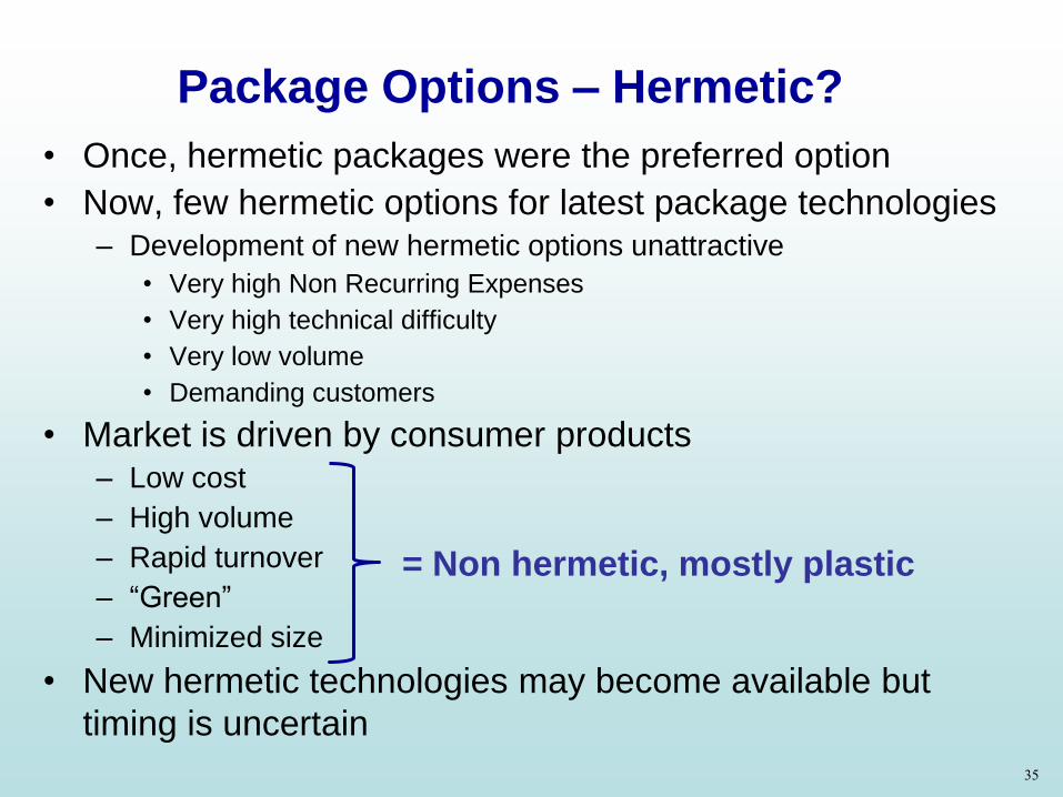
• Once, hermetic packages were the preferred option
• Now, few hermetic options for latest package technologies– Development of new hermetic options unattractive
• Very high Non Recurring Expenses
• Very high technical difficulty
• Very low volume
• Demanding customers
• Market is driven by consumer products– Low cost
– High volume
– Rapid turnover
– ―Green‖
– Minimized size
• New hermetic technologies may become available but
timing is uncertain
= Non hermetic, mostly plastic
35
Package Options – Hermetic?

36
• Typically, packages consist of the same basic
features but achieve them in many ways:
– Functional elements - active die, passives etc.
– Interconnects between elements (2 or more elements)
– A substrate
– Interconnects to the external I/O of the package
– A protective package
– Interconnects to the next higher level of assembly
The “General” Package

Lunar Reconnaissance Orbiter (LRO), Built at GSFC,
Launched with LCROSS, June 18,2009
37
• I/O s, increasing number, decreasing pitch
• Heat Dissipation, (especially in space)
• Manufacturability
• Materials
• Mechanical
• Installation
• Testability
• Inspectability
• RoHS (Pb-free)
• (Space Environment)
Continuous Packaging Challenges

Die
Underfill
Flip Chip
Die Bump
Capacitor,
Resistor etc.
Substrate
Multi-layer Encapsulation
Pb-free
Ball
* PBGA: Plastic Ball
Grid Array
38
Commercial, Non-hermetic Package (PBGA*)
Design Drivers:
• High I/O count
• Large die
• Environmental protection
• Performance/Speed
• Ancillary parts
Commercial Drivers:
• Low cost
• High volume
• Limited life
• Automated installation
• Compact

ONE STRIKE
AND YOU’RE
OUT!
39
• Vacuum:
– Outgassing, offgassing, property deterioration
• Foreign Object Debris (FOD)
– From the package threat to the system, or a threat to the package
• Shock and vibration
– During launch, deployments and operation
• Thermal cycling
– Usually small range; high number of cycles in Low Earth Orbit (LEO)
• Thermal management
– Only conduction and radiation transfer heat
• Thousands of interconnects
– Opportunities for opens, intermittent - possibly latent
• Low volume assembly
– Limited automation, lots of rework
• Long life
– Costs for space are high, make the most of the investment
• Novel hardware
– Lots of ―one offs‖
• Rigorous test and inspection
– To try to find the latent threats to reliability
Space Challenges for Complex
Non-hermetic Packages

Space Challenge Some Defenses
Vacuum Low out/off-gassing materials. Ceramics vs polymers.
Shock and vibration Compliant / robust interconnects - wire bonds, solder balls, columns, conductive polymer
Thermal cycling Compliant/robust interconnects, matched thermal expansion coefficients
Thermal management Heat spreader in the lid and/or substrate, thermally conductive materials
Thousands of interconnects Process control, planarity, solderability, substrate design
Low volume assembly Remains a challenge
Long life Good design, materials, parts and process control
Novel hardware Test, test, test
Rigorous test and
inspection
Testability and inspectability will always be challenges
Cover
Die
Flip Chip Die
Bump
Capacitor,
Resistor etc.
“Enclosed”
Package
OptionUnderfill
Substrate and
Sn/Pb Column
Grid Array
* Ceramic Column
Grid Array
40
Non-hermetic Package, With”Space”
Features (CCGA*?)

• NASA prefers hermetic packages for critical
applications
• Hermeticity is measureable, assuring package
integrity
• Only 3 tests provide assurance for hermetic
package integrity:
– Hermeticity – nothing bad can get in
– Residual or Internal gas analysis – nothing bad is inside
– Particle Impact Noise Detection – no FOD inside
• NON-HERMETIC PACKAGE INTEGRITY IS HARD
TO ASSESS - NO 3 BASIC TESTS
• Non-hermetic packages expose materials’
interfaces that are locked away in hermetic ones
41
Hermeticity

But What is Hermetic?
• Per MIL-PRF-38534 Appx E and 38535 Appx A, hermetic
packages must consist of metals, ceramic and glass in
combinations ONLY, no polymerics
• Meets aggressive leak rate test limits
– Verifies low rate of gas escape/ atmospheric interchange
– Even so, small volume packages meeting “tight limits”
theoretically exchange their atmosphere very quickly:• 0.001 cc, exchanges 93% in 1 month at 5X10⁻⁸ atmosphere/cc/sec!
• 1.0cc, 96% in 10 years at 1 X 10⁻⁸
– Even large packages with quite small leaks can surprise• 10 cc, 96% in 1 year at 1 X 10⁻⁶ !
• For applications in space vacuum why care?
– Risk for contamination on the ground
– Risk for outgassing in vacuum
42

43
• Current and future package options mix and match
elements in almost infinite combinations
• Elements include:– Wire bonds
– Ball interconnects
– Solder joints
– Conductive epoxies
– Vias
– Multi-layer substrates
– Multiple chips, active and passive (hybrid?)
– Stacking of components
– Embedded actives and passives
– Polymers
– Ceramics
– Enclosures/encapsulants
– Thermal control features
Non-hermetic Package Variations

From Amkor’s Website http://www.amkor.com/go/packaging
44
Some Large Device Package Options

45
More Complexity is Coming
• Stacking of chips to provide a third dimension of
density and complexity– Stacking of Field Programmable Gate Arrays (FPGAs)
appears imminent
– Stacking of memory die is “old hat”
– Through-silicon vias instead of bond wires• Maintain speed and allow lots of I/Os
• High volumetric efficiency
– Significant manufacturability challenges • Material and dimensional interfaces
• Testability
– Significant usability challenges• Design complexity
• Handling, testing, rework/replace, risk management
• Cost versus benefit trades

46
MIL-PRF-38535, Class Y
• “Y Not” Non-hermetic for Space?
• Proposed new class for M38535, monolithic microcircuits
• Class Y will be for Space level non-hermetic
• Class V will be defined as hermetic only
• Addition to Appendix B, “Space Application”
• Package-specific “integrity” test requirements proposed by manufacturer, approved by DLA* and government space
• The Package Integrity Test Plan must address:
– Potential materials degradation
– Interconnect reliability
– Thermal management
– Resistance to processing stresses
– Thermo-mechanical stresses
• G12 Task Group established 01/13/10
* MIL spec qualifying activity Defense Logistics Agency, Land and Maritime

47
NEPP Activities
• Continuous surveillance of emerging trends
• Have evaluated embedded passives
– Partnering with Navy Crane
– Quite mature technologies, bulk capacitive layer
– Works but ―space‖ low quantities a challenge
• Have tried to evaluate a novel, flexible, embedded
active-die technology
– Considerable promise
– Beset by technical problems, particularly die thinning
– Consider revisiting as technology improves
• Initial evaluations of technical readiness of die
thinning, through-hole vias and advance die stacking
are needed
• Continue development of Class Y concept

48
Section 4
Other Information

Para 6.4.28 Class N. Items which have been subjected to and passed
all applicable requirements of this specification including
qualification testing, screening testing, and TCI/QCI inspections, and
are encapsulated in plastic. This product must be assessed by the
user to determine if it is appropriate for use in users’ application.
Para 6.4.29 Class Q. Items (add “that are hermetic and”) which have been
subjected to and passed all applicable requirements of this
specification and applicable appendices including qualification
testing, screening testing, and TCI/QCI inspections.
(Note: The only known exception would be non-hermetic 5962-
9760805(thru 09)QYA 32-bit RISC processors.)
Para 6.4.30 Class V. Items that (add “are hermetic and”) meet all the
class Q requirements, and have been subjected to, and passed all
applicable requirements of appendix B herein.
Ref: MIL-PRF-38535, Rev J
MIL-PRF38535 Class Definitions
49

50
• The NEPP mission is to provide guidance to
NASA for the selection and application of
microelectronics and other parts
technologies, to improve understanding of
the risks related to the use of these
technologies in the space environment and
to ensure that appropriate research is
performed to meet NASA mission assurance
needs.
• NEPP subset: NASA Electronic Parts
Assurance Group (NEPAG)
• Focuses on daily needs of parts
assurance knowledge-base
NASA Technology Readiness
Levels (TRLs)
NEPP
interest
range
NEPAG
interest
range
NEPP/NEPAG Mission and Focus

• Military standards for microcircuits haven’t kept pace with developments in
packaging technology
• RADC (Rome Air Development Center) and later RAC (Rome Air Center) used
to be the technical arm of DLA (Defense Logistic Agency) and they did
necessary evaluations to keep up with new developments.
• NEPAG (NASA EEE Parts Assurance Group), which is like a large component
engineering group representing space agencies, is addressing these issues:
• 38535 Appendix H, new technology evaluation, update (L. Harzstark).
• Requirement for screening of passive elements was added to 38535.
• An out-of-box approach was taken for non-hermetic parts, e.g., V-4;
concept of a new class, ―Class Y‖ (M. Sampson)
• 3 new JC13 task groups formed 38535.
• Support to 13.4: power MOSFETs, other (K. LaBel)
Some NEPAG Activities:
• Weekly Telecons
• Supplier Audits
• DLA Land & Maritime SMD reviews
• Others
NEPAG Contribution to MIL-STD
51