
NCP5392 - 2/3/4-Phase Controller for CPU Applications
33
Semiconductor Components Industries, LLC, 2010 November, 2010 - Rev. 4 1 Publication Order Number: NCP5392/D NCP5392 2/3/4--Phase Controller for CPU Applications The NCP5392 provides up to a four-phase buck solution which combines differential voltage sensing, differential phase current sensing, and adaptive voltage positioning to provide accurately regulated power for both Intel and AMD processors. Dual-edge pulse-width modulation (PWM) combined with inductor current sensing reduces system cost by providing the fastest initial response to dynamic load events. Dual -edge multiphase modulation reduces the total bulk and ceramic output capacitance required to meet transient regulation specifications. A high performance operational error amplifier is provided to simplify compensation of the system. Dynamic Reference Injection further simplifies loop compensation by eliminating the need to compromise between closed-loop transient response and Dynamic VID performance. Features Meets Intel’s VR11.1 Specifications Meets AMD 6 Bit Code Specifications Dual-edge PWM for Fastest Initial Response to Transient Loading High Performance Operational Error Amplifier Internal Soft Start Dynamic Reference Injection DAC Range from 0.375 V to 1.6 V DAC Feed Forward 0.5% DAC Voltage Accuracy from 1.0 V to 1.6 V True Differential Remote Voltage Sensing Amplifier Phase -to-Phase Current Balancing “Lossless” Differential Inductor Current Sensing Differential Current Sense Amplifiers for each Phase Adaptive Voltage Positioning (AVP) Oscillator Frequency Range of 100 kHz – 1 MHz Latched Over Voltage Protection (OVP) Guaranteed Startup into Pre-Charged Loads Threshold Sensitive Enable Pin for VTT Sensing Power Good Output with Internal Delays Thermally Compensated Current Monitoring This is a Pb -Free Device Applications Desktop Processors 40 PIN QFN, 6x6 MN SUFFIX CASE 488AR Device Package Shipping † ORDERING INFORMATION NCP5392MNR2G* QFN--40 (Pb--Free) 2500/Tape & Reel MARKING DIAGRAM NCP5392 = Specific Device Code A = Assembly Location WL = Wafer Lot YY = Year WW = Work Week G = Pb--Free Package NCP5392 AWLYYWWG 1 http://onsemi.com †For information on tape and reel specifications, including part orientation and tape sizes, please refer to our Tape and Reel Packaging Specification Brochure, BRD8011/D. *Pin 41 is the thermal pad on the bottom of the device. *Temperature Range: 0C to 85C 40 1
Transcript of NCP5392 - 2/3/4-Phase Controller for CPU Applications

Semiconductor Components Industries, LLC, 2010
November, 2010 -- Rev. 41 Publication Order Number:
NCP5392/D
NCP5392
2/3/4--Phase Controller forCPU ApplicationsThe NCP5392 provides up to a four--phase buck solution which
combines differential voltage sensing, differential phase currentsensing, and adaptive voltage positioning to provide accuratelyregulated power for both Intel and AMD processors. Dual--edgepulse--width modulation (PWM) combined with inductor currentsensing reduces system cost by providing the fastest initial responseto dynamic load events. Dual--edge multiphase modulation reducesthe total bulk and ceramic output capacitance required to meettransient regulation specifications.A high performance operational error amplifier is provided to
simplify compensation of the system. Dynamic Reference Injectionfurther simplifies loop compensation by eliminating the need tocompromise between closed--loop transient response and DynamicVID performance.
Features Meets Intel’s VR11.1 Specifications
Meets AMD 6 Bit Code Specifications
Dual--edge PWM for Fastest Initial Response to Transient Loading High Performance Operational Error Amplifier
Internal Soft Start
Dynamic Reference Injection
DAC Range from 0.375 V to 1.6 V
DAC Feed Forward
0.5% DAC Voltage Accuracy from 1.0 V to 1.6 V True Differential Remote Voltage Sensing Amplifier
Phase--to--Phase Current Balancing
“Lossless” Differential Inductor Current Sensing
Differential Current Sense Amplifiers for each Phase Adaptive Voltage Positioning (AVP)
Oscillator Frequency Range of 100 kHz – 1 MHz
Latched Over Voltage Protection (OVP) Guaranteed Startup into Pre--Charged Loads
Threshold Sensitive Enable Pin for VTT Sensing
Power Good Output with Internal Delays Thermally Compensated Current Monitoring
This is a Pb--Free Device
Applications Desktop Processors
40 PIN QFN, 6x6MN SUFFIXCASE 488AR
Device Package Shipping†
ORDERING INFORMATION
NCP5392MNR2G* QFN--40(Pb--Free)
2500/Tape & Reel
MARKINGDIAGRAM
NCP5392 = Specific Device CodeA = Assembly LocationWL = Wafer LotYY = YearWW = Work WeekG = Pb--Free Package
NCP5392AWLYYWWG
1
http://onsemi.com
†For information on tape and reel specifications,including part orientation and tape sizes, pleaserefer to our Tape and Reel Packaging SpecificationBrochure, BRD8011/D.
*Pin41 is the thermalpadon thebottomof thedevice.
*Temperature Range: 0C to 85C
401
NCP5392
http://onsemi.com2
G130
DRVON29
CS428
CS4N27
CS326
CS3N25
CS224
CS2N23
CS122
CS1N21
VR_H
OT
40
VR_R
DY
39
NTC
38
PSI
37
DAC
36
VCC
35
12VMON
34
G4
33
G3
32
G2
31
EN1
VID02
VID13
VID24
VID35
VID46
VID57
VID68
VID79
ROSC10
ILIM
11
IMON
12
VSP
13
VSN
14
DIFFOUT
15
COMP
16
VFB
17
VDRP
18
VDFB
19
CSSUM
20
NCP5392
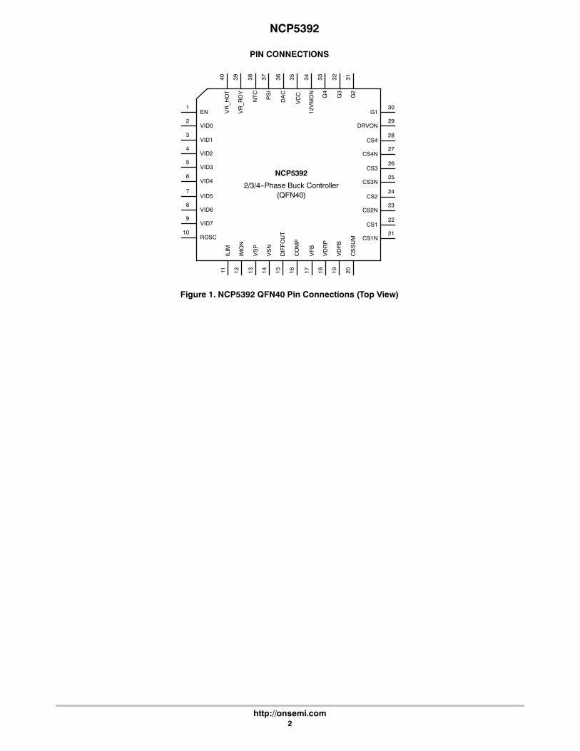
PIN CONNECTIONS
2/3/4--Phase Buck Controller(QFN40)
Figure 1. NCP5392 QFN40 Pin Connections (Top View)

NCP5392
http://onsemi.com3
G1
+
--
G2
G3
OvervoltageProtection
+
--
G4
Control,Fault Logic
andMonitorCircuits
IMON
DRVON
PSI
NTCVR_HOT
VR_RDY
UVLO
ILimit
4.25 V
+
--
+
--
+
--
+
--
+
ROSC
CS4N
CS4P
CS3N
CS3P
GND (FLAG)
CS2N
CS2P
CS1N
CS1P
CSSUM
VDFB
VDRP
COMP
VFB
DIFFOUT
VSP
VSN
VID7/AMDVID6VID5VID4VID3VID2VID1VID0
Flexible DAC
Droop Amp
Error Amp
+--
Diff Amp
+
--
1.3 V+--
+
+
+
Oscillator
Gain = 6
+--
Gain = 6
Gain = 6
Gain = 6
+--
+--
+--
+
ILIM
EN
VCC
DAC
Figure 2. NCP5392 Block Diagram
+
+
+
+
--
12VMON
--2/3

NCP5392
http://onsemi.com4
CPUGND
12V_FILTER12V_FILTER
NCP5359
VCC
OD
IN
BST
DRH
SW
DRL
PGND
12V_FILTER12V_FILTER
NCP5359
VCC
OD
IN
BST
DRH
SW
DRL
PGND
12V_FILTER12V_FILTER
NCP5359
VCC
OD
IN
BST
DRH
SW
DRL
PGND
12V_FILTER12V_FILTER
NCP5359
VCC
OD
IN
BST
DRH
SW
DRL
PGND
RT1
RNTC1
IMON
PSI
NTC
IMON
38
12
PSI
VCC
12VMON
373534
12V_FILTER+5V
VID0
VID1
VID2
VID3
VID4
VID5
VID6
VID7
VTT
2
3
4
5
6
7
8
9
1
39
40
14
13
15
16
17
18
19
20
36
EN
VR_RDY
VR_HOT
VSN
VSP
DIFFOUT
COMP
VFB
VDRP
VDFB
CSSUM
DAC
GND
ILIM
ROSC
41 11 10
RLIM1
RLIM2
RISO1 RISO2RT2
CDFB
RNOR R6R6
CDNI
RDNP
CH
RF
RFB1
RFB
CF
CFB1
RDRP
30
22
21
31
24
23
32
26
25
33
28
27
29
G1
CS1P
CS1N
G2
CS2P
CS2N
G3
CS3P
CS3N
G4
CS4P
CS4N
DRVON
VCCP
VSSN
Figure 3. Application Schematic for Four Phases
NCP5392
+
Q1
Q2 R2 RS1
CS1C2
C4
C3
D1
C1
L1
NCP5392
http://onsemi.com5
CPUGND
12V_FILTER12V_FILTER
NCP5359
VCC
OD
IN
BST
DRH
SW
DRL
PGND
12V_FILTER12V_FILTER
NCP5359
VCC
OD
IN
BST
DRH
SW
DRL
PGND
12V_FILTER12V_FILTER
NCP5359
VCC
OD
IN
BST
DRH
SW
DRL
PGND
RT1
RNTC1
IMON
PSI
NTC
IMON
38
12
PSI
VCC
12VMON
373534
12V_FILTER+5V
VID0
VID1
VID2
VID3
VID4
VID5
VID6
VID7
VTT
2
3
4
5
6
7
8
9
1
39
40
14
13
15
16
17
18
19
20
36
EN
VR_RDY
VR_HOT
VSN
VSP
DIFFOUT
COMP
VFB
VDRP
VDFB
CSSUM
DAC
GND
ILIM
ROSC
41 11 10
RLIM1
RLIM2
RISO1 RISO2RT2
CDFB
RNOR R6R6
CDNI
RDNP
CH
RF
RFB1
RFB
CF
CFB1
RDRP
30
22
21
31
24
23
32
26
25
33
28
27
29
G1
CS1P
CS1N
G2
CS2P
CS2N
G3
CS3P
CS3N
G4
CS4P
CS4N
DRVON
VCCP
VSSN
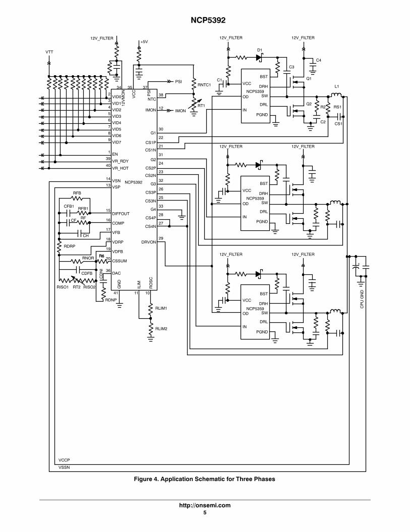
Figure 4. Application Schematic for Three Phases
NCP5392
+
C4
L1
RS1R2
C2
Q2
Q1
D1
C3
CS1
C1

NCP5392
http://onsemi.com6
CPUGND
12V_FILTER12V_FILTER
NCP5359
VCC
OD
IN
BST
DRH
SW
DRL
PGND
12V_FILTER12V_FILTER
NCP5359
VCC
OD
IN
BST
DRH
SW
DRL
PGND
RT1
RNTC1
IMON
PSI
NTC
IMON
38
12
PSI
VCC
12VMON
373534
12V_FILTER+5V
VID0
VID1
VID2
VID3
VID4
VID5
VID6
VID7
VTT
2
3
4
5
6
7
8
9
1
39
40
14
13
15
16
17
18
19
20
36
EN
VR_RDY
VR_HOT
VSN
VSP
DIFFOUT
COMP
VFB
VDRP
VDFB
CSSUM
DAC
GND
ILIM
ROSC
41 11 10
RLIM1
RLIM2
RISO1 RISO2RT2
CDFB
RNOR R6R6
CDNI
RDNP
CH
RF
RFB1
RFB
CF
CFB1
RDRP
30
22
21
31
24
23
32
26
25
33
28
27
29
G1
CS1P
CS1N
G2
CS2P
CS2N
G3
CS3P
CS3N
G4
CS4P
CS4N
DRVON
VCCP
VSSN
Figure 5. Application Schematic for Two Phases
NCP5392
+
C4
L1
RS1R2
C2
Q2
Q1
D1
C3
CS1
C1

NCP5392
http://onsemi.com7
PIN DESCRIPTIONS
Pin No. Symbol Description
1 EN Threshold sensitive input. High = startup, Low = shutdown.
2 VID0 Voltage ID DAC input
3 VID1 Voltage ID DAC input
4 VID2 Voltage ID DAC input
5 VID3 Voltage ID DAC input
6 VID4 Voltage ID DAC input
7 VID5 Voltage ID DAC input
8 VID6 Voltage ID DAC input
9 VID7/AMD Voltage ID DAC input. Pull to VCC (5 V) to enable AMD 6--bit DAC code.
10 ROSC A resistance from this pin to ground programs the oscillator frequency according to fSW. This pin supplies atrimmed output voltage of 2 V.
11 ILIM Overcurrent shutdown threshold setting. Connect this pin to the ROSC pin via a resistor divider as shown inthe Application Schematics. To disable the overcurrent feature, connect this pin directly to the ROSC pin. Toguarantee correct operation, this pin should only be connected to the voltage generated by the ROSC pin; donot connect this pin to any externally generated voltages.
12 IMON 0 mV to 900 mV analog signal proportional to the output load current. VSN referenced
13 VSP Non--inverting input to the internal differential remote sense amplifier
14 VSN Inverting input to the internal differential remote sense amplifier
15 DIFFOUT Output of the differential remote sense amplifier
16 COMP Output of the error amplifier
17 VFB Compensation Amplifier Voltage feedback
18 VDRP Voltage output signal proportional to current used for current limit and output voltage droop
19 VDFB Droop Amplifier Voltage Feedback
20 CSSUM Inverted Sum of the Differential Current Sense inputs. Av=CSSUM/CSx = --4
21 CS1N Inverting input to current sense amplifier #1
22 CS1 Non--inverting input to current sense amplifier #1
23 CS2N Inverting input to current sense amplifier #2
24 CS2 Non--inverting input to current sense amplifier #2
25 CS3N Inverting input to current sense amplifier #3
26 CS3 Non--inverting input to current sense amplifier #3
27 CS4N Inverting input to current sense amplifier #4
28 CS4 Non--inverting input to current sense amplifier #4
29 DRVON Bidirectional Gate Drive Enable
30 G1 PWM output pulse to gate driver. 3--level output: Low = LSFET Enabled, Mid = Diode Emulation Enabled,High = HSFET Enabled
31 G2 PWM output pulse to gate driver. 3--level output (see G1)
32 G3 PWM output pulse to gate driver. 3--level output (see G1)
33 G4 PWM output pulse to gate driver. 3--level output (see G1)
34 12VMON Monitor a 12 V input through a resistor divider.
35 VCC Power for the internal control circuits.
36 DAC DAC Feed Forward Output
37 PSI Power Saving Control. Low = single phase operation, High = normal operation.
38 NTC Threshold sensitive input for thermal monitoring
39 VR_RDY Open collector output. High indicates that the output is regulating
40 VR_HOT Open collector output indicates the state of the thermal monitoring input. Low impedance output indicating anormal status when the voltage of NTC pin is above the specified threshold. This pin will transition to highimpedance when the voltage of NTC pin decrease (temperature increase) below the specified threshold.This pin requires an external pullup resistor
FLAG GND Power supply return (QFN Flag)
NCP5392
http://onsemi.com8
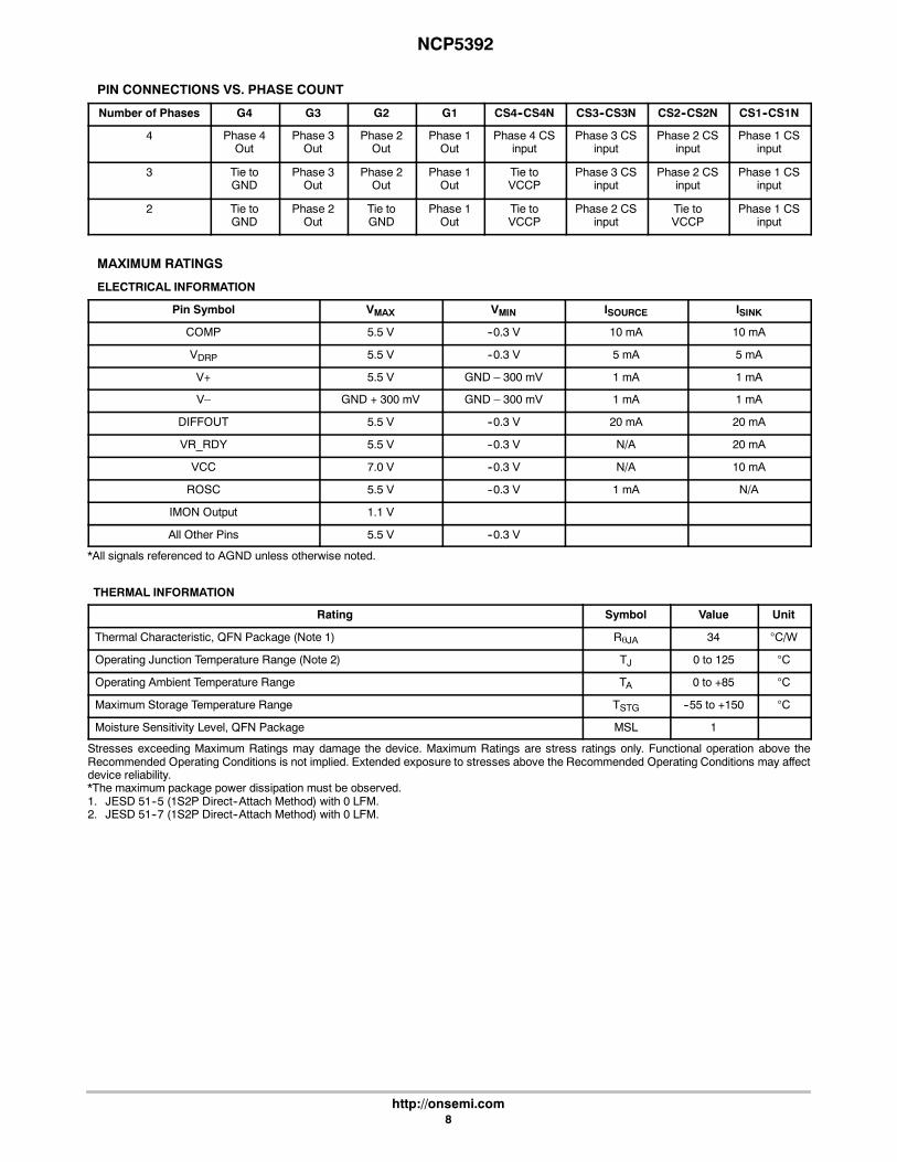
PIN CONNECTIONS VS. PHASE COUNT
Number of Phases G4 G3 G2 G1 CS4--CS4N CS3--CS3N CS2--CS2N CS1--CS1N
4 Phase 4Out
Phase 3Out
Phase 2Out
Phase 1Out
Phase 4 CSinput
Phase 3 CSinput
Phase 2 CSinput
Phase 1 CSinput
3 Tie toGND
Phase 3Out
Phase 2Out
Phase 1Out
Tie toVCCP
Phase 3 CSinput
Phase 2 CSinput
Phase 1 CSinput
2 Tie toGND
Phase 2Out
Tie toGND
Phase 1Out
Tie toVCCP
Phase 2 CSinput
Tie toVCCP
Phase 1 CSinput
MAXIMUM RATINGS
ELECTRICAL INFORMATION
Pin Symbol VMAX VMIN ISOURCE ISINK
COMP 5.5 V --0.3 V 10 mA 10 mA
VDRP 5.5 V --0.3 V 5 mA 5 mA
V+ 5.5 V GND – 300 mV 1 mA 1 mA
V– GND + 300 mV GND – 300 mV 1 mA 1 mA
DIFFOUT 5.5 V --0.3 V 20 mA 20 mA
VR_RDY 5.5 V --0.3 V N/A 20 mA
VCC 7.0 V --0.3 V N/A 10 mA
ROSC 5.5 V --0.3 V 1 mA N/A
IMON Output 1.1 V
All Other Pins 5.5 V --0.3 V
*All signals referenced to AGND unless otherwise noted.
THERMAL INFORMATION
Rating Symbol Value Unit
Thermal Characteristic, QFN Package (Note 1) RθJA 34 C/W
Operating Junction Temperature Range (Note 2) TJ 0 to 125 C
Operating Ambient Temperature Range TA 0 to +85 C
Maximum Storage Temperature Range TSTG --55 to +150 C
Moisture Sensitivity Level, QFN Package MSL 1
Stresses exceeding Maximum Ratings may damage the device. Maximum Ratings are stress ratings only. Functional operation above theRecommended Operating Conditions is not implied. Extended exposure to stresses above the Recommended Operating Conditions may affectdevice reliability.*The maximum package power dissipation must be observed.1. JESD 51--5 (1S2P Direct--Attach Method) with 0 LFM.2. JESD 51--7 (1S2P Direct--Attach Method) with 0 LFM.

NCP5392
http://onsemi.com9
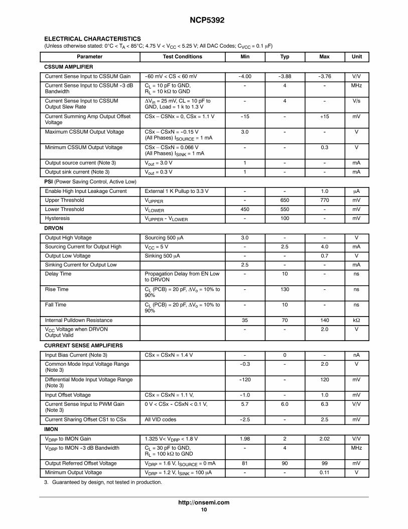
ELECTRICAL CHARACTERISTICS(Unless otherwise stated: 0C < TA < 85C; 4.75 V < VCC < 5.25 V; All DAC Codes; CVCC = 0.1 mF)
Parameter Test Conditions Min Typ Max Unit
ERROR AMPLIFIER
Input Bias Current (Note 3) --200 200 nA
Noninverting Voltage Range (Note 3) 0 1.3 3 V
Input Offset Voltage (Note 3) V+ = V-- = 1.1 V --1.0 -- 1.0 mV
Open Loop DC Gain CL = 60 pF to GND,RL = 10 KΩ to GND
-- 100 dB
Open Loop Unity Gain Bandwidth CL = 60 pF to GND,RL = 10 KΩ to GND
-- 10 -- MHz
Open Loop Phase Margin CL = 60 pF to GND,RL = 10 KΩ to GND
-- 80 --
Slew Rate ΔVin = 100 mV, G = -- 10 V/V,ΔVout = 1.5 V – 2.5 V,CL = 60 pF to GND,DC Load = 125 mA to GND
-- 5 -- V/ms
Maximum Output Voltage ISOURCE = 2.0 mA 3.5 -- -- V
Minimum Output Voltage ISINK = 0.2 mA -- -- 50 mV
Output source current (Note 3) Vout = 3.5 V 2 -- -- mA
Output sink current (Note 3) Vout = 1.0 V 2 -- -- mA
DIFFERENTIAL SUMMING AMPLIFIER
VSN Input Bias Current VSN Voltage = 0 V 30 mA
VSP Input Resistance DRVON = LowDRVON = High
1.517
kΩ
VSP Input Bias Voltage DRVON = LowDRVON = High
0.090.66
V
Input Voltage Range (Note 3) --0.3 -- 3.0 V
--3 dB Bandwidth CL = 80 pF to GND,RL = 10 KΩ to GND
-- 10 -- MHz
Closed Loop DC Gain VS to Diffout VS+ to VS-- = 0.5 to 1.6 V 0.98 1.0 1.025 V/V
Maximum Output Voltage ISOURCE = 2 mA 3.0 -- -- V
Minimum Output Voltage ISINK = 2 mA -- -- 0.5 V
Output source current (Note 3) Vout = 3 V 2.0 -- -- mA
Output sink current (Note 3) Vout = 0.5 V 2.0 -- -- mA
INTERNAL OFFSET VOLTAGE
Offset Voltage to the (+) Pin of theError Amp and the VDRP pin
-- 1.30 -- V
VDROOP AMPLIFIER
Input Bias Current (Note 3) --200 200 nA
Non--inverting Voltage Range (Note 3) 0 1.3 3 V
Input Offset Voltage (Note 3) V+ = V-- = 1.1 V --4.0 -- 4.0 mV
Open Loop DC Gain CL = 20 pF to GND includingESD, RL = 1 kΩ to GND
-- 100 dB
Open Loop Unity Gain Bandwidth CL = 20 pF to GND includingESD, RL = 1 kΩ to GND
-- 10 -- MHz
Slew Rate CL = 20 pF to GND includingESD, RL = 1 kΩ to GND
-- 5 -- V/ms
Maximum Output Voltage ISOURCE = 4.0 mA 3 -- -- V
Minimum Output Voltage ISINK = 1.0 mA -- -- 1 V
Output source current (Note 3) Vout = 3.0 V 4 -- -- mA
Output sink current (Note 3) Vout = 1.0 V 1 -- -- mA
3. Guaranteed by design, not tested in production.
NCP5392
http://onsemi.com10
ELECTRICAL CHARACTERISTICS(Unless otherwise stated: 0C < TA < 85C; 4.75 V < VCC < 5.25 V; All DAC Codes; CVCC = 0.1 mF)
Parameter UnitMaxTypMinTest Conditions
CSSUM AMPLIFIER
Current Sense Input to CSSUM Gain --60 mV < CS < 60 mV --4.00 --3.88 --3.76 V/V
Current Sense Input to CSSUM --3 dBBandwidth
CL = 10 pF to GND,RL = 10 kΩ to GND
-- 4 -- MHz
Current Sense Input to CSSUMOutput Slew Rate
ΔVin = 25 mV, CL = 10 pF toGND, Load = 1 k to 1.3 V
-- 4 -- V/s
Current Summing Amp Output OffsetVoltage
CSx – CSNx = 0, CSx = 1.1 V --15 -- +15 mV
Maximum CSSUM Output Voltage CSx – CSxN = --0.15 V(All Phases) ISOURCE = 1 mA
3.0 -- -- V
Minimum CSSUM Output Voltage CSx – CSxN = 0.066 V(All Phases) ISINK = 1 mA
-- -- 0.3 V
Output source current (Note 3) Vout = 3.0 V 1 -- -- mA
Output sink current (Note 3) Vout = 0.3 V 1 -- -- mA
PSI (Power Saving Control, Active Low)
Enable High Input Leakage Current External 1 K Pullup to 3.3 V -- -- 1.0 mA
Upper Threshold VUPPER -- 650 770 mV
Lower Threshold VLOWER 450 550 -- mV
Hysteresis VUPPER -- VLOWER -- 100 -- mV
DRVON
Output High Voltage Sourcing 500 mA 3.0 -- -- V
Sourcing Current for Output High VCC = 5 V -- 2.5 4.0 mA
Output Low Voltage Sinking 500 mA -- -- 0.7 V
Sinking Current for Output Low 2.5 -- -- mA
Delay Time Propagation Delay from EN Lowto DRVON
-- 10 -- ns
Rise Time CL (PCB) = 20 pF, ΔVo = 10% to90%
-- 130 -- ns
Fall Time CL (PCB) = 20 pF, ΔVo = 10% to90%
-- 10 -- ns
Internal Pulldown Resistance 35 70 140 kΩ
VCC Voltage when DRVONOutput Valid
-- -- 2.0 V
CURRENT SENSE AMPLIFIERS
Input Bias Current (Note 3) CSx = CSxN = 1.4 V -- 0 -- nA
Common Mode Input Voltage Range(Note 3)
--0.3 -- 2.0 V
Differential Mode Input Voltage Range(Note 3)
--120 -- 120 mV
Input Offset Voltage CSx = CSxN = 1.1 V, --1.0 -- 1.0 mV
Current Sense Input to PWM Gain(Note 3)
0 V < CSx -- CSxN < 0.1 V, 5.7 6.0 6.3 V/V
Current Sharing Offset CS1 to CSx All VID codes --2.5 -- 2.5 mV
IMON
VDRP to IMON Gain 1.325 V< VDRP < 1.8 V 1.98 2 2.02 V/V
VDRP to IMON --3 dB Bandwidth CL = 30 pF to GND,RL = 100 kΩ to GND
-- 4 MHz
Output Referred Offset Voltage VDRP = 1.6 V, ISOURCE = 0 mA 81 90 99 mV
Minimum Output Voltage VDRP = 1.2 V, ISINK = 100 mA -- -- 0.11 V
3. Guaranteed by design, not tested in production.

NCP5392
http://onsemi.com11
ELECTRICAL CHARACTERISTICS(Unless otherwise stated: 0C < TA < 85C; 4.75 V < VCC < 5.25 V; All DAC Codes; CVCC = 0.1 mF)
Parameter UnitMaxTypMinTest Conditions
IMON
Output source current (Note 3) Vout = 1 V 300 -- -- mA
Output sink current (Note 3) Vout = 0.3 V 300 -- -- mA
Maximum Clamp Voltage VDRP Voltage = 2 V,RLOAD = 100 k
-- -- 1.15 V
OSCILLATOR
Switching Frequency Range (Note 3) 100 -- 1000 kHz
Switching Frequency Accuracy 2-- or4--Phase
ROSC = 49.9 kΩ 200 -- 224 kHz
ROSC = 24.9 kΩ 374 -- 414
ROSC = 10 kΩ 800 -- 978
Switching Frequency Accuracy3--Phase
ROSC = 49.9 kΩ 191 -- 234 kHz
ROSC = 24.9 kΩ 354 -- 434
ROSC = 10 kΩ 755 -- 1000
ROSC Output Voltage 1.95 2.01 2.065 V
MODULATORS (PWM Comparators)
Minimum Pulse Width FSW = 800 KHz -- 30 -- ns
Propagation Delay 20 mV of Overdrive -- 10 -- ns
0% Duty Cycle COMP Voltage when the PWMOutputs Remain LO
-- 1.3 -- V
100% Duty Cycle COMP Voltage when the PWMOutputs Remain HI
-- 2.3 -- V
PWM Ramp Duty Cycle Matching Between Any Two Phases -- 90 -- %
PWM Phase Angle Error (Note 3) Between Adjacent Phases 15 -- 15
VR_RDY (POWER GOOD) OUTPUT
VR_RDY Output Saturation Voltage IPGD = 10 mA, -- -- 0.4 V
VR_RDY Rise Time (Note 3) External Pullup of 1 kΩ to 1.25V, CTOT = 45 pF, ΔVo = 10% to90%
-- 100 150 ns
VR_RDY Output Voltage at Powerup(Note 3)
VR_RDY Pulled up to 5 V via2 kΩ, tR(VCC) 3 x tR(5V)100 ms tR(VCC) 20 ms
-- -- 1.0 V
VR_RDY High – Output LeakageCurrent (Note 3)
VR_RDY = 5.5 V via 1 K -- -- 0.2 mA
VR_RDY Upper Threshold Voltage VCore Increasing, DAC = 1.3 V -- 310 270 mVBelowDAC
VR_RDY Lower Threshold Voltage VCore DecreasingDAC = 1.3 V
410 370 mVBelowDAC
VR_RDY Rising Delay VCore Increasing -- 500 -- ms
VR_RDY Falling Delay VCore Decreasing -- 5 -- ms
PWM OUTPUTS
Output High Voltage Sourcing 500 mA 3.0 -- -- V
Mid Output Voltage 1.4 1.5 1.6 V
Output Low Voltage Sinking 500 mA -- -- 0.7 V
Delay + Fall Time (Note 3) CL (PCB) = 50 pF,ΔVo = VCC to GND
-- 10 15 ns
Delay + Rise Time (Note 3) CL (PCB) = 50 pF,ΔVo = GND to VCC
-- 10 15 ns
3. Guaranteed by design, not tested in production.

NCP5392
http://onsemi.com12
ELECTRICAL CHARACTERISTICS(Unless otherwise stated: 0C < TA < 85C; 4.75 V < VCC < 5.25 V; All DAC Codes; CVCC = 0.1 mF)
Parameter UnitMaxTypMinTest Conditions
PWM OUTPUTS
Output Impedance – HI or LO State Resistance to VCC (HI) or GND(LO)
-- 75 -- Ω
2/3/4--PhASE DETECTION
Gate Pin Source Current 60 80 150 mA
Gate Pin Threshold Voltage 210 240 265 mV
Phase Detect Timer 15 20 27 ms
DIGITAL SOFT--START
Soft--Start Ramp Time DAC = 0 to DAC = 1.1 V 1.0 -- 1.5 ms
VR11 Vboot time 400 500 600 ms
VID7/VR11/AMD INPUT
VID Upper Threshold VUPPER -- 650 800 mV
VID Lower Threshold VLOWER 300 550 -- mV
VID Hysteresis VUPPER -- VLOWER -- 100 -- mV
AMD Input Bias Current 10 -- 20 mA
VR11 Input Bias Current (Note 3) 200 nA
Delay before Latching VID Change(VID De--Skewing) (Note 3)
Measured from the edge of the1st VID change
200 -- 300 ns
AMD Upper Threshold (Note 3) 2.9 V
AMD Lower Threshold (Note 3) 2.4 V
ENABLE INPUT
Enable High Input Leakage Current(Note 3)
Pullup to 1.3 V -- -- 200 nA
VR11 Rising Threshold -- 650 770 mV
VR11 Falling Threshold 450 550 -- mV
VR11 Total Hysteresis Rising-- Falling Threshold -- 100 -- mV
AMD Upper Threshold -- 1.3 1.5 V
AMD Lower Threshold 0.9 1.1 -- V
AMD Total Hysteresis Rising -- Falling Threshold 200 mV
Enable Delay Time Measure Time from EnableTransitioning HI to when OutputBegins
2.5 4.0 ms
CURRENT LIMIT
ILIM to VDRP Gain Between VDRP -- VDFB = 450 mVand VDRP -- VDFB = 650 mV
0.95 1 1.05 V/V
ILIM to VDRP Gain in PSI 4 phase Between VDRP -- VDFB = 450 mVand VDRP -- VDFB = 650 mV
-- 0.25 -- V/V
ILIM to VDRP Gain in PSI 3 phase Between VDRP -- VDFB = 450 mVand VDRP -- VDFB = 650 mV
-- 0.33 -- V/V
ILIM to VDRP Gain in PSI 2 phase Between VDRP -- VDFB = 450 mVand VDRP -- VDFB = 650 mV
-- 0.5 -- V/V
ILIM Offset VDRP -- VDFB = 520 mV --50 0 50 mV
Delay -- 100 -- ns
OVERVOLTAGE PROTECTION
VR11 Overvoltage Threshold DAC +150 DAC +185 DAC +200 mV
VR11 PSI Overvoltage Threshold(Note 3)
(1.6 V DAC)+150
(1.6 V DAC)+200
mV
AMD Overvoltage Threshold (Note 3) DAC +200 DAC +235 DAC +305 mV
3. Guaranteed by design, not tested in production.

NCP5392
http://onsemi.com13
ELECTRICAL CHARACTERISTICS(Unless otherwise stated: 0C < TA < 85C; 4.75 V < VCC < 5.25 V; All DAC Codes; CVCC = 0.1 mF)
Parameter UnitMaxTypMinTest Conditions
OVERVOLTAGE PROTECTION
AMD PSI Overvoltage Threshold(Note 3)
(1.55 V DAC)+200
(1.55 V DAC)+235
(1.55 V DAC)+305
mV
Delay 100 ns
UNDERVOLTAGE PROTECTION
VCC UVLO Start Threshold 4 4.25 4.5 V
VCC UVLO Stop Threshold 3.8 4.05 4.3 V
VCC UVLO Hysteresis 200 mV
VR_HOT
VR_HOT Upper Voltage Threshold 19.6 kΩ P.U. to VCC, 68 kΩNTC,β = 3740
0.257 0.268 0.280 VCC
VR_HOT Lower Voltage Threshold 19.6 kΩ P.U. to VCC, 68 KΩNTC,β = 3740
0.316 0.329 0.343 VCC
VR_HOT Output Voltages atPower--up (Note 3)
External Pull--up resistor of 2 KΩto 5 V, tR_VCC 3 x tR_5 V,100 ms tR_VCC 20 ms
-- -- 1.0 V
VR_HOT Saturation Output Voltage ISINK = 4 mA -- -- 0.3 V
VR_HOT Output Leakage Current -- -- 1 mA
NTC Pin Bias Current -- -- 1 mA
12VMON UVLO
12VMON (High Threshold) VCC Valid -- 0.77 0.82 V
12VMON (Low Threshold) VCC Valid 0.66 0.68 -- V
DAC (FEED FORWARD FUNCTION)
Output Source Current VOUT = 3 V 0.25 mA
Output Sink Current VOUT = 0.3 V 1.5 mA
Max Output Voltage (Note 3) Isource = 2 mA 3 V
Min Output Voltage (Note 3) Isink = 2 mA 0.5 V
VRM 11 DAC
Positive DAC Slew Rate 11 -- 16.5 mV/ms
System Voltage Accuracy(DAC Value has a 19 mV Offset Overthe Output Value)
1.0 V < DAC < 1.6 V0.8 V < DAC < 1.0 V0.5 V < DAC < 0.8 V
------
------
0.558
%mVmV
AMD DAC
Positive DAC Slew Rate -- 3.5 5 mV/ms
System Voltage Accuracy(DAC Value has a 19 mV Offset Overthe Output Value)
1.0 V < DAC < 1.55 V0.3750 < DAC < 0.8 V
-- -- 0.55.0
%mV
VCC
VCC Operating Current EN Low, No PWM -- 15 30 mA
3. Guaranteed by design, not tested in production.

NCP5392
http://onsemi.com14
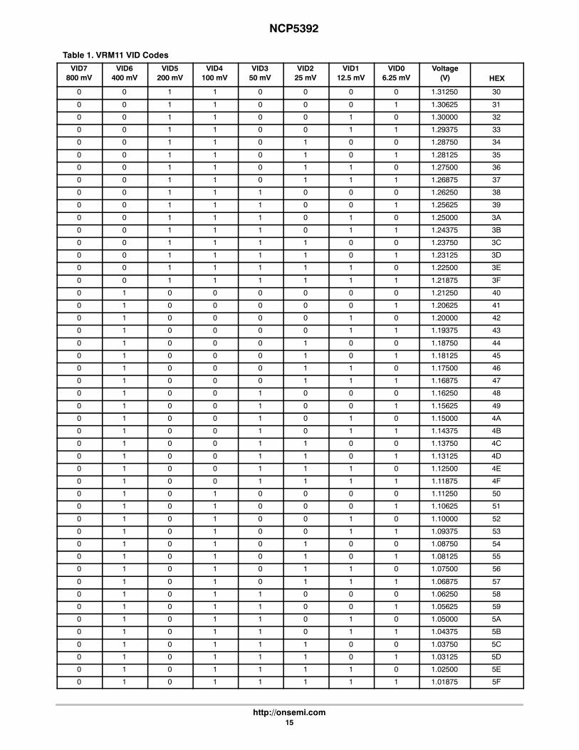
Table 1. VRM11 VID Codes
VID7800 mV
VID6400 mV
VID5200 mV
VID4100 mV
VID350 mV
VID225 mV
VID112.5 mV
VID06.25 mV
Voltage(V) HEX
0 0 0 0 0 0 0 0 00
0 0 0 0 0 0 0 1 01
0 0 0 0 0 0 1 0 1.60000 02
0 0 0 0 0 0 1 1 1.59375 03
0 0 0 0 0 1 0 0 1.58750 04
0 0 0 0 0 1 0 1 1.58125 05
0 0 0 0 0 1 1 0 1.57500 06
0 0 0 0 0 1 1 1 1.56875 07
0 0 0 0 1 0 0 0 1.56250 08
0 0 0 0 1 0 0 1 1.55625 09
0 0 0 0 1 0 1 0 1.55000 0A
0 0 0 0 1 0 1 1 1.54375 0B
0 0 0 0 1 1 0 0 1.53750 0C
0 0 0 0 1 1 0 1 1.53125 0D
0 0 0 0 1 1 1 0 1.52500 0E
0 0 0 0 1 1 1 1 1.51875 0F
0 0 0 1 0 0 0 0 1.51250 10
0 0 0 1 0 0 0 1 1.50625 11
0 0 0 1 0 0 1 0 1.50000 12
0 0 0 1 0 0 1 1 1.49375 13
0 0 0 1 0 1 0 0 1.48750 14
0 0 0 1 0 1 0 1 1.48125 15
0 0 0 1 0 1 1 0 1.47500 16
0 0 0 1 0 1 1 1 1.46875 17
0 0 0 1 1 0 0 0 1.46250 18
0 0 0 1 1 0 0 1 1.45625 19
0 0 0 1 1 0 1 0 1.45000 1A
0 0 0 1 1 0 1 1 1.44375 1B
0 0 0 1 1 1 0 0 1.43750 1C
0 0 0 1 1 1 0 1 1.43125 1D
0 0 0 1 1 1 1 0 1.42500 1E
0 0 0 1 1 1 1 1 1.41875 1F
0 0 1 0 0 0 0 0 1.41250 20
0 0 1 0 0 0 0 1 1.40625 21
0 0 1 0 0 0 1 0 1.40000 22
0 0 1 0 0 0 1 1 1.39375 23
0 0 1 0 0 1 0 0 1.38750 24
0 0 1 0 0 1 0 1 1.38125 25
0 0 1 0 0 1 1 0 1.37500 26
0 0 1 0 0 1 1 1 1.36875 27
0 0 1 0 1 0 0 0 1.36250 28
0 0 1 0 1 0 0 1 1.35625 29
0 0 1 0 1 0 1 0 1.35000 2A
0 0 1 0 1 0 1 1 1.34375 2B
0 0 1 0 1 1 0 0 1.33750 2C
0 0 1 0 1 1 0 1 1.33125 2D
0 0 1 0 1 1 1 0 1.32500 2E
0 0 1 0 1 1 1 1 1.31875 2F
NCP5392
http://onsemi.com15
Table 1. VRM11 VID Codes
VID7800 mV HEX
Voltage(V)
VID06.25 mV
VID112.5 mV
VID225 mV
VID350 mV
VID4100 mV
VID5200 mV
VID6400 mV
0 0 1 1 0 0 0 0 1.31250 30
0 0 1 1 0 0 0 1 1.30625 31
0 0 1 1 0 0 1 0 1.30000 32
0 0 1 1 0 0 1 1 1.29375 33
0 0 1 1 0 1 0 0 1.28750 34
0 0 1 1 0 1 0 1 1.28125 35
0 0 1 1 0 1 1 0 1.27500 36
0 0 1 1 0 1 1 1 1.26875 37
0 0 1 1 1 0 0 0 1.26250 38
0 0 1 1 1 0 0 1 1.25625 39
0 0 1 1 1 0 1 0 1.25000 3A
0 0 1 1 1 0 1 1 1.24375 3B
0 0 1 1 1 1 0 0 1.23750 3C
0 0 1 1 1 1 0 1 1.23125 3D
0 0 1 1 1 1 1 0 1.22500 3E
0 0 1 1 1 1 1 1 1.21875 3F
0 1 0 0 0 0 0 0 1.21250 40
0 1 0 0 0 0 0 1 1.20625 41
0 1 0 0 0 0 1 0 1.20000 42
0 1 0 0 0 0 1 1 1.19375 43
0 1 0 0 0 1 0 0 1.18750 44
0 1 0 0 0 1 0 1 1.18125 45
0 1 0 0 0 1 1 0 1.17500 46
0 1 0 0 0 1 1 1 1.16875 47
0 1 0 0 1 0 0 0 1.16250 48
0 1 0 0 1 0 0 1 1.15625 49
0 1 0 0 1 0 1 0 1.15000 4A
0 1 0 0 1 0 1 1 1.14375 4B
0 1 0 0 1 1 0 0 1.13750 4C
0 1 0 0 1 1 0 1 1.13125 4D
0 1 0 0 1 1 1 0 1.12500 4E
0 1 0 0 1 1 1 1 1.11875 4F
0 1 0 1 0 0 0 0 1.11250 50
0 1 0 1 0 0 0 1 1.10625 51
0 1 0 1 0 0 1 0 1.10000 52
0 1 0 1 0 0 1 1 1.09375 53
0 1 0 1 0 1 0 0 1.08750 54
0 1 0 1 0 1 0 1 1.08125 55
0 1 0 1 0 1 1 0 1.07500 56
0 1 0 1 0 1 1 1 1.06875 57
0 1 0 1 1 0 0 0 1.06250 58
0 1 0 1 1 0 0 1 1.05625 59
0 1 0 1 1 0 1 0 1.05000 5A
0 1 0 1 1 0 1 1 1.04375 5B
0 1 0 1 1 1 0 0 1.03750 5C
0 1 0 1 1 1 0 1 1.03125 5D
0 1 0 1 1 1 1 0 1.02500 5E
0 1 0 1 1 1 1 1 1.01875 5F

NCP5392
http://onsemi.com16
Table 1. VRM11 VID Codes
VID7800 mV HEX
Voltage(V)
VID06.25 mV
VID112.5 mV
VID225 mV
VID350 mV
VID4100 mV
VID5200 mV
VID6400 mV
0 1 1 0 0 0 0 0 1.01250 60
0 1 1 0 0 0 0 1 1.00625 61
0 1 1 0 0 0 1 0 1.00000 62
0 1 1 0 0 0 1 1 0.99375 63
0 1 1 0 0 1 0 0 0.98750 64
0 1 1 0 0 1 0 1 0.98125 65
0 1 1 0 0 1 1 0 0.97500 66
0 1 1 0 0 1 1 1 0.96875 67
0 1 1 0 1 0 0 0 0.96250 68
0 1 1 0 1 0 0 1 0.95625 69
0 1 1 0 1 0 1 0 0.95000 6A
0 1 1 0 1 0 1 1 0.94375 6B
0 1 1 0 1 1 0 0 0.93750 6C
0 1 1 0 1 1 0 1 0.93125 6D
0 1 1 0 1 1 1 0 0.92500 6E
0 1 1 0 1 1 1 1 0.91875 6F
0 1 1 1 0 0 0 0 0.91250 70
0 1 1 1 0 0 0 1 0.90625 71
0 1 1 1 0 0 1 0 0.90000 72
0 1 1 1 0 0 1 1 0.89375 73
0 1 1 1 0 1 0 0 0.88750 74
0 1 1 1 0 1 0 1 0.88125 75
0 1 1 1 0 1 1 0 0.87500 76
0 1 1 1 0 1 1 1 0.86875 77
0 1 1 1 1 0 0 0 0.86250 78
0 1 1 1 1 0 0 1 0.85625 79
0 1 1 1 1 0 1 0 0.85000 7A
0 1 1 1 1 0 1 1 0.84375 7B
0 1 1 1 1 1 0 0 0.83750 7C
0 1 1 1 1 1 0 1 0.83125 7D
0 1 1 1 1 1 1 0 0.82500 7E
0 1 1 1 1 1 1 1 0.81875 7F
1 0 0 0 0 0 0 0 0.81250 80
1 0 0 0 0 0 0 1 0.80625 81
1 0 0 0 0 0 1 0 0.80000 82
1 0 0 0 0 0 1 1 0.79375 83
1 0 0 0 0 1 0 0 0.78750 84
1 0 0 0 0 1 0 1 0.78125 85
1 0 0 0 0 1 1 0 0.77500 86
1 0 0 0 0 1 1 1 0.76875 87
1 0 0 0 1 0 0 0 0.76250 88
1 0 0 0 1 0 0 1 0.75625 89
1 0 0 0 1 0 1 0 0.75000 8A
1 0 0 0 1 0 1 1 0.74375 8B
1 0 0 0 1 1 0 0 0.73750 8C
1 0 0 0 1 1 0 1 0.73125 8D
1 0 0 0 1 1 1 0 0.72500 8E
1 0 0 0 1 1 1 1 0.71875 8F

NCP5392
http://onsemi.com17
Table 1. VRM11 VID Codes
VID7800 mV HEX
Voltage(V)
VID06.25 mV
VID112.5 mV
VID225 mV
VID350 mV
VID4100 mV
VID5200 mV
VID6400 mV
1 0 0 1 0 0 0 0 0.71250 90
1 0 0 1 0 0 0 1 0.70625 91
1 0 0 1 0 0 1 0 0.70000 92
1 0 0 1 0 0 1 1 0.69375 93
1 0 0 1 0 1 0 0 0.68750 94
1 0 0 1 0 1 0 1 0.68125 95
1 0 0 1 0 1 1 0 0.67500 96
1 0 0 1 0 1 1 1 0.66875 97
1 0 0 1 1 0 0 0 0.66250 98
1 0 0 1 1 0 0 1 0.65625 99
1 0 0 1 1 0 1 0 0.65000 9A
1 0 0 1 1 0 1 1 0.64375 9B
1 0 0 1 1 1 0 0 0.63750 9C
1 0 0 1 1 1 0 1 0.63125 9D
1 0 0 1 1 1 1 0 0.62500 9E
1 0 0 1 1 1 1 1 0.61875 9F
1 0 1 0 0 0 0 0 0.61250 A0
1 0 1 0 0 0 0 1 0.60625 A1
1 0 1 0 0 0 1 0 0.60000 A2
1 0 1 0 0 0 1 1 0.59375 A3
1 0 1 0 0 1 0 0 0.58750 A4
1 0 1 0 0 1 0 1 0.58125 A5
1 0 1 0 0 1 1 0 0.57500 A6
1 0 1 0 0 1 1 1 0.56875 A7
1 0 1 0 1 0 0 0 0.56250 A8
1 0 1 0 1 0 0 1 0.55625 A9
1 0 1 0 1 0 1 0 0.55000 AA
1 0 1 0 1 0 1 1 0.54375 AB
1 0 1 0 1 1 0 0 0.53750 AC
1 0 1 0 1 1 0 1 0.53125 AD
1 0 1 0 1 1 1 0 0.52500 AE
1 0 1 0 1 1 1 1 0.51875 AF
1 0 1 1 0 0 0 0 0.51250 B0
1 0 1 1 0 0 0 1 0.50625 B1
1 0 1 1 0 0 1 0 0.50000 B2
1 1 1 1 1 1 1 0 OFF FE
1 1 1 1 1 1 1 1 OFF FF

NCP5392
http://onsemi.com18
Table 2. AMD Processor 6--bit VID Code
(VID) Codes Nominal Vout Units
VID5 VID4 VID3 VID2 VID1 VID0
0 0 0 0 0 0 1.550 V
0 0 0 0 0 1 1.525 V
0 0 0 0 1 0 1.500 V
0 0 0 0 1 1 1.475 V
0 0 0 1 0 0 1.450 V
0 0 0 1 0 1 1.425 V
0 0 0 1 1 0 1.400 V
0 0 0 1 1 1 1.375 V
0 0 1 0 0 0 1.350 V
0 0 1 0 0 1 1.325 V
0 0 1 0 1 0 1.300 V
0 0 1 0 1 1 1.275 V
0 0 1 1 0 0 1.250 V
0 0 1 1 0 1 1.225 V
0 0 1 1 1 0 1.200 V
0 0 1 1 1 1 1.175 V
0 1 0 0 0 0 1.150 V
0 1 0 0 0 1 1.125 V
0 1 0 0 1 0 1.100 V
0 1 0 0 1 1 1.075 V
0 1 0 1 0 0 1.050 V
0 1 0 1 0 1 1.025 V
0 1 0 1 1 0 1.000 V
0 1 0 1 1 1 0.975 V
0 1 1 0 0 0 0.950 V
0 1 1 0 0 1 0.925 V
0 1 1 0 1 0 0.900 V
0 1 1 0 1 1 0.875 V
0 1 1 1 0 0 0.850 V
0 1 1 1 0 1 0.825 V
0 1 1 1 1 0 0.800 V
0 1 1 1 1 1 0.775 V
1 0 0 0 0 0 0.7625 V
1 0 0 0 0 1 0.7500 V
1 0 0 0 1 0 0.7375 V
1 0 0 0 1 1 0.7250 V
1 0 0 1 0 0 0.7125 V
1 0 0 1 0 1 0.7000 V
1 0 0 1 1 0 0.6875 V
1 0 0 1 1 1 0.6750 V
1 0 1 0 0 0 0.6625 V

NCP5392
http://onsemi.com19
Table 2. AMD Processor 6--bit VID Code
(VID) Codes UnitsNominal Vout
VID5 VID0VID1VID2VID3VID4
1 0 1 0 0 1 0.6500 V
1 0 1 0 1 0 0.6375 V
1 0 1 0 1 1 0.6250 V
1 0 1 1 0 0 0.6125 V
1 0 1 1 0 1 0.6000 V
1 0 1 1 1 0 0.5875 V
1 0 1 1 1 1 0.5750 V
1 1 0 0 0 0 0.5625 V
1 1 0 0 0 1 0.5500 V
1 1 0 0 1 0 0.5375 V
1 1 0 0 1 1 0.5250 V
1 1 0 1 0 0 0.5125 V
1 1 0 1 0 1 0.5000 V
1 1 0 1 1 0 0.4875 V
1 1 0 1 1 1 0.4750 V
1 1 1 0 0 0 0.4625 V
1 1 1 0 0 1 0.4500 V
1 1 1 0 1 0 0.4375 V
1 1 1 0 1 1 0.4250 V
1 1 1 1 0 0 0.4125 V
1 1 1 1 0 1 0.4000 V
1 1 1 1 1 0 0.3875 V
1 1 1 1 1 1 0.3750 V

NCP5392
http://onsemi.com20
FUNCTIONAL DESCRIPTION
GeneralThe NCP5392 provides up to four--phase buck solution
which combines differential voltage sensing, differentialphase current sensing, and adaptive voltage positioning toprovide accurately regulated power necessary for bothIntel VR11.1 and AMDCPU power system. NCP5392 hasbeen designed to work with the NCP5359 driver.
Remote Output Sensing Amplifier(RSA)A true differential amplifier allows the NCP5392 to
measure Vcore voltage feedback with respect to the Vcoreground reference point by connecting the Vcore referencepoint to VSP, and the Vcore ground reference point to VSN.This configuration keeps ground potential differencesbetween the local controller ground and the Vcore groundreference point from affecting regulation of Vcore betweenVcore and Vcore ground reference points. The RSA alsosubtracts the DAC (minus VID offset) voltage, therebyproducing an unamplified output error voltage at theDIFFOUT pin. This output also has a 1.3 V bias voltage asthe floating ground to allow both positive and negativeerror voltages.
Precision Programmable DACA precision programmable DAC is provided and system
trimmed. This DAC has 0.5% accuracy over the entireoperating temperature range of the part. The DAC can beprogrammed to support either Intel VR11 or AMD 6--bitVID code specifications.
High Performance Voltage Error AmplifierThe error amplifier is designed to provide high slew rate
and bandwidth. Although not required when operating asthe controller of a voltage regulator, a capacitor fromCOMP to VFB is required for stable unity gain testconfigurations.
Gate Driver Outputs and 2/3/4 Phase OperationThe part can be configured to run in 2--, 3--, or 4--phase
mode. In 2--phase mode, phases 1 and 3 should be used todrive the external gate drivers as shown in the 2--phaseApplications Schematic, G2 and G4 must be grounded. In3--phase mode, gate output G4must be grounded as shownin the 3--phase Applications Schematic. In 4--phase modeall 4 gate outputs are used as shown in the 4--phaseApplications Schematic. The Current Sense inputs ofunused channels should be connected to VCCP shown inthe Application Schematics. Please refer to table “PINCONNECTIONS vs. PHASE COUNTS” for details.
Differential Current Sense Amplifiers and SummingAmplifierFour differential amplifiers are provided to sense the
output current of each phase. The inputs of each currentsense amplifier must be connected across the currentsensing element of the phase controlled by thecorresponding gate output (G1, G2, G3, or G4). If a phaseis unused, the differential inputs to that phase’s currentsense amplifier must be shorted together and connected tothe output as shown in the 2-- and 3--phase ApplicationSchematics.The current signals sensed from inductor DCR are fed into
a summing amplifier to have a summed--up output (CSSUM).Signal of CSSUMcombines information of total current of allphases in operation.The outputs of current sense amplifiers control three
functions. First, the summing current signal (CCSUM) ofall phases will go through DROOP amplifier and join thevoltage feedback loop for output voltage positioning.Second, the output signal fromDROOPamplifier also goesto ILIM amplifier to monitor the output current limit.Finally, the individual phase current contributes to thecurrent balance of all phases by offsetting their rampsignals of PWM comparators.
Thermal Compensation Amplifier with VDRP and VDFBPinsThermal compensation amplifier is an internal amplifier
in the path of droop current feedback for additionaladjustment of the gain of summing current and temperaturecompensation. The way thermal compensation isimplemented separately ensures minimum interference tothe voltage loop compensation network.
Oscillator and Triangle Wave GeneratorA programmable precision oscillator is provided. The
oscillator’s frequency is programmed by the resistanceconnected from the ROSC pin to ground. The user willusually form this resistance from two resistors in order tocreate a voltage divider that uses the ROSC output voltageas the reference for creating the current limit setpointvoltage. The oscillator frequency range is 100 kHz perphase to 1.0 MHz per phase. The oscillator generates up to4 symmetrical triangle waveformswith amplitude between1.3 V and 2.3 V. The triangle waves have a phase delaybetween them such that for 2--, 3-- and 4--phase operationthe PWMoutputs are separated by 180, 120, and 90 angulardegrees, respectively.

NCP5392
http://onsemi.com21
PWM Comparators with HysteresisFour PWM comparators receive an error signal at their
noninverting input. Each comparator receives one of thetriangle waves at its inverting output. The output of eachcomparator generates the PWM outputs G1, G2, G3, andG4.During steady state operation, the duty cycle will center
on the valley of the triangle waveform, with steady stateduty cycle calculated by Vout/Vin. During a transient event,both high and low comparator output transitions shift phaseto the points where the error signal intersects the down andup ramp of the triangle wave.
PROTECTION FEATURES
Undervoltage Lockout (VCC and 12VMON)An undervoltage lockout (UVLO) senses the VCC input
directly. 12 V UVLO senses the 12 V power supply byconnecting it to the 12VMON pin through an appropriateresistor divider. During power--up, both the VCC input and12VMON are monitored, and the PWM outputs and thesoft--start circuit are disabled until both input voltagesexceed the threshold voltages of their individual UVLOcomparators. The UVLO comparators both incorporatehysteresis to avoid chattering.
Overcurrent ShutdownA programmable overcurrent function is incorporated
within the IC. A comparator and latch make up thisfunction. The inverting input of the comparator isconnected to the ILIM pin. The voltage at this pin sets themaximum output current the converter can produce. TheROSC pin provides a convenient and accurate referencevoltage from which a resistor divider can create theovercurrent setpoint voltage. Although not actuallydisabled, tying the ILIM pin directly to the ROSC pin setsthe limit above useful levels -- effectively disablingovercurrent shutdown. The comparator noninverting inputis the summed current information from the VDRP minusoffset voltage. The overcurrent latch is set when the currentinformation exceeds the voltage at the ILIM pin. Theoutputs are pulled low, and the soft--start is pulled low. Theoutputs will remain disabled until the VCC voltage isremoved and re--applied, or the ENABLE input is broughtlow and then high.
Output Overvoltage and Undervoltage Protection andPower Good MonitorAn output voltage monitor is incorporated. During
normal operation, if the output voltage is 180 mV (typical)over the DACvoltage, the VR_RDYgoes low, theDRVONsignal remains high, the PWM outputs are set low. Theoutputs will remain disabled until the VCC voltage isremoved and reapplied. During normal operation, if theoutput voltage falls more than 350 mV below the DACsetting, the VR_RDY pin will be set low until the outputvoltage rises.
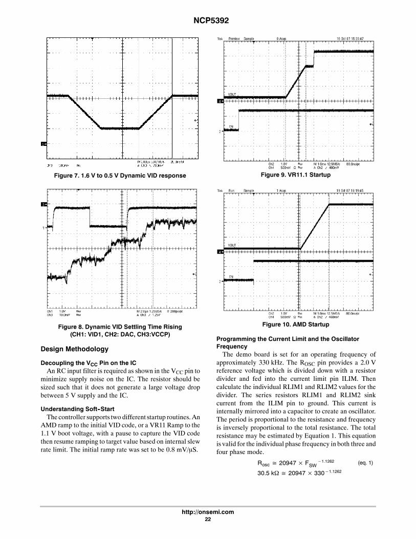
Soft--StartThere are two possible soft--start modes: AMD and
VR11. AMD mode simply ramps Vcore from 0 V directlyto the DAC setting at a fixed rate. The VR11 mode rampsVcore to 1.1 V boot voltage at a fixed rate of 0.8 mV/mS,pauses at 1.1 V for around 500 mS, reads the VID pins todetermine the DAC setting. Then ramps Vcore to the finalDAC setting at the Dynamic VID slew rate of up to12.5 mV/mS. Typical AMD and VR11 soft--start sequencesare shown in the following graphs (Figure 9 and 10).
APPLICATION INFORMATIONThe NCP5392 demo board for the NCP5392 is available
by request. It is configured as a four phase solution withdecoupling designed to provide a 1 mΩ load line under a100 A step load.
Startup ProcedureStart by installing the test tool software. It is best to
power the test tool from a separate ATX power supply. Thetest tool should be set to a valid VID code of 0.5 V or abovein order for the controller to start. Consult the VTT helpmanual for more detailed instruction.
Step Load TestingThe VTT tool is used to generate the di/dt step load.
Select the dynamic loading option in the VTT test toolsoftware. Set the desired step load size, frequency, duty,and slew rate. See Figure 6.
Figure 6. Typical Load Step Response(full load, 35 A -- 100 A)
Dynamic VID TestingThe VTT tool provides for VID stepping based on the
Intel Requirements. Select the Dynamic VID option.Before enabling the test set the lowest VID to 0.5 V orgreater and set the highestVID to a value that is greater thanthe lowest VID selection, then enable the test. See Figures7 and 8.
NCP5392
http://onsemi.com22
Figure 7. 1.6 V to 0.5 V Dynamic VID response
Figure 8. Dynamic VID Settling Time Rising(CH1: VID1, CH2: DAC, CH3:VCCP)
Design Methodology
Decoupling the VCC Pin on the ICAn RC input filter is required as shown in the VCC pin to
minimize supply noise on the IC. The resistor should besized such that it does not generate a large voltage dropbetween 5 V supply and the IC.
Understanding Soft--StartThe controller supports two different startup routines.An
AMD ramp to the initial VID code, or a VR11 Ramp to the1.1 V boot voltage, with a pause to capture the VID codethen resume ramping to target value based on internal slewrate limit. The initial ramp rate was set to be 0.8 mV/mS.
Figure 9. VR11.1 Startup
Figure 10. AMD Startup
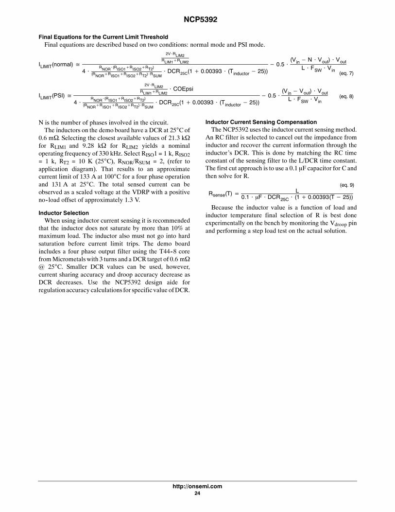
Programming the Current Limit and the OscillatorFrequencyThe demo board is set for an operating frequency of
approximately 330 kHz. The ROSC pin provides a 2.0 Vreference voltage which is divided down with a resistordivider and fed into the current limit pin ILIM. Thencalculate the individual RLIM1 and RLIM2 values for thedivider. The series resistors RLIM1 and RLIM2 sinkcurrent from the ILIM pin to ground. This current isinternally mirrored into a capacitor to create an oscillator.The period is proportional to the resistance and frequencyis inversely proportional to the total resistance. The totalresistance may be estimated by Equation 1. This equationis valid for the individual phase frequency in both three andfour phase mode.
Rosc ≅ 20947× FSW−1.1262 (eq. 1)
30.5 kΩ≅ 20947× 330−1.1262

NCP5392
http://onsemi.com23
0
10
20
30
40
50
60
100 1000Freq--kHz
Rosc--kohm
CalculationReal
Figure 11. ROSC vs. Frequency
The current limit function is based on the total sensedcurrent of all phases multiplied by a controlled gain(Acssum*Adrp). DCR sensed inductor current is a functionof the winding temperature. The best approach is to set themaximum current limit based on expected averagemaximum temperature of the inductor windings,
DCRTmax = DCR25C(1+ 0.00393 ⋅ (Tmax− 25)) (eq. 2)
For multiphase controller, the ripple current can be calculated as,
Ipp=(Vin− N ⋅ Vout) ⋅ Vout
L ⋅ FSW ⋅ Vin(eq. 3)
Therefore calculate the current limit voltage as below,
VLIMIT ≅ ACSSUM ⋅ ADRP ⋅DCRTmax ⋅ (IMIN_OCP ⋅ + 0.5 ⋅ Ipp) (eq. 4)
VLIMIT ≅ ACSSUM ⋅ ADRP ⋅DCRTmax ⋅ IMIN_OCP ⋅ + 0.5 ⋅(Vin− N ⋅ Vout) ⋅ Vout
L ⋅ FSW ⋅ Vin
In Equation 4, ACSSUM and ADRP are the gain of current summing amplifier and droop amplifier.
Figure 12. ACSSUM and ADRP
+
I1
I2I3I4
Ilim
Acssum Adrp
OCPevent
+--
+--
RISO1 RISO2RT2
RSUM
RNOR
As introduced before, VLIMIT comes from a resistordivider connected to Rosc pin, thus,
VLIMIT = 2 V ⋅RLIM2
RLIM1+RLIM2⋅COEpsi (eq. 5)
ACSSUM=−4
ADRP=−RNOR ⋅ (RISO1+ RISO2+ RT2)
(RNOR+ RISO1+ RISO2+ RT2) ⋅RSUM(eq. 6)
RISO1 and RISO2 are in series with RT2, the NTCtemperature sense resistor placed near inductor. RSUM isthe resistor connecting between pin VDFB and pinCSSUM. If PSI = 1, PSI function is off, the current limitfollows the Equation 7; if PSI = 0, the power saving modewill be enabled, COEpsi is a coefficient for the currentlimiting related with power saving function (PSI), thecurrent limit can be calculated from Equation 8. COEpsivalue is one over the original phase count N. Refer to thePSI and phase shedding section for more details.
NCP5392
http://onsemi.com24
Final Equations for the Current Limit ThresholdFinal equations are described based on two conditions: normal mode and PSI mode.
ILIMIT(normal)≅
2V⋅RLIM2RLIM1+RLIM2
4 ⋅RNOR⋅(RISO1+RISO2+RT2)
(RNOR+RISO1+RISO2+RT2)⋅RSUM⋅DCR25C(1+ 0.00393 ⋅ (Tinductor− 25))
− 0.5 ⋅(Vin−N ⋅ Vout) ⋅ Vout
L ⋅ FSW ⋅ Vin(eq. 7)
ILIMIT(PSI)≅
2V⋅RLIM2RLIM1+RLIM2
⋅COEpsi
4 ⋅RNOR⋅(RISO1+RISO2+RT2)
(RNOR+RISO1+RISO2+RT2)⋅RSUM⋅DCR25C(1+ 0.00393 ⋅ (Tinductor− 25))
− 0.5 ⋅(Vin− Vout) ⋅ VoutL ⋅ FSW ⋅ Vin
(eq. 8)
N is the number of phases involved in the circuit.The inductors on the demo board have a DCR at 25C of
0.6 mΩ. Selecting the closest available values of 21.3 kΩfor RLIM1 and 9.28 kΩ for RLIM2 yields a nominaloperating frequency of 330 kHz. Select RISO1 = 1 k, RISO2= 1 k, RT2 = 10 K (25C), RNOR/RSUM = 2, (refer toapplication diagram). That results to an approximatecurrent limit of 133 A at 100C for a four phase operationand 131 A at 25C. The total sensed current can beobserved as a scaled voltage at the VDRP with a positiveno--load offset of approximately 1.3 V.
Inductor SelectionWhen using inductor current sensing it is recommended
that the inductor does not saturate by more than 10% atmaximum load. The inductor also must not go into hardsaturation before current limit trips. The demo boardincludes a four phase output filter using the T44--8 corefromMicrometalswith 3 turns and a DCR target of 0.6 mΩ@ 25C. Smaller DCR values can be used, however,current sharing accuracy and droop accuracy decrease asDCR decreases. Use the NCP5392 design aide forregulation accuracy calculations for specific value ofDCR.
Inductor Current Sensing CompensationThe NCP5392 uses the inductor current sensing method.
An RC filter is selected to cancel out the impedance frominductor and recover the current information through theinductor’s DCR. This is done by matching the RC timeconstant of the sensing filter to the L/DCR time constant.The first cut approach is to use a 0.1 mF capacitor for C andthen solve for R.
Rsense(T)=L
0.1 ⋅ mF ⋅DCR25C ⋅ (1+ 0.00393(T− 25))
(eq. 9)
Because the inductor value is a function of load andinductor temperature final selection of R is best doneexperimentally on the bench by monitoring the Vdroop pinand performing a step load test on the actual solution.

NCP5392
http://onsemi.com25
Simple Average SPICE ModelA simple state average model shown in Figure 13 can be used to determine a stable solution and provide insight into the
control system.
Figure 13. NCP5392 Average SPICE Model
RSUM1k
--
++--
E1
EGAIN = {6}
L
{185e--9/4}1 2
RDFB
2k
LBRD
100p1 2DCR
{0.6E--3/4}
RBRD
0.75m
ESRBulk{7e--3/6}
Voff
ESLBulk{3.5e--9/6}
1
2
CBulk{560e--6*6}
ESRCer{1.5e--3/18}
ESLCer{1.5e--9/18}
1
2
CCer{22e--6*18}
I1TD = 100u
TF = 50nPW = 100uPER = 200u
I1 = 50I2 = 110
TR = 50n0Adc0Aac
0
R9
1kC6
10.6p
120
VRamp_min1.3V
Voffset1.3V
R10
2k
RFB
1k
RFB1
69.8RF
2.2k
CFB1
680P
CH
22pCF1.8n
R125.11k
{--2/3*4}
1E3 R6
1kC410.6p
R11
1k
V312V
0
Voff
0
0
0
0
0
1E3
0
GAIN = 1
R8
1kC510.6p
Vdrp
Voff
CDAC
12n VDACAC = 0
TRAN = PULSE
DC = 1.2V
RDAC
50
Vdrp
Vout
Unity Gain BW=15MHz
Voff
CDFB22p
1E3
IMON
(0 0.05 400u 5u 5u 500u 1000u)
Compensation and Output Filter DesignIf the required output filter and switching frequency are
significantly different, it’s best to use the available PSPICEmodels to design the compensation and output filter fromscratch.The design target for this demo board was 1.0 mΩ up to
2.0 MHz. The phase switching frequency is currently set to330 kHz. It can easily be seen that the board impedance of0.75 mΩ between the load and the bulk capacitance has alarge effect on the output filter. In this case the six 560 mFbulk capacitors have an ESR of 7.0 mΩ. Thus the bulk ESR
plus the board impedance is 1.15 mΩ + 0.75 mΩ or1.9 mΩ. The actual output filter impedance does not dropto 1.0 mΩ until the ceramic breaks in at over 375 kHz. Thecontroller must provide some loop gain slightly less thanone out to a frequency in excess 300 kHz. At frequenciesbelow where the bulk capacitance ESR breaks with thebulk capacitance, the DC--DC converter must havesufficiently high gain to control the output impedancecompletely. Standard Type--3 compensation works wellwith the NCP5392.

NCP5392
http://onsemi.com26
Figure 14. NCP5392 Circuit Frequency Response
--100
--80
--60
--40
--20
0
20
40
60
80
100 1000 10000 100000 1000000 10000000
Frequency
dB
Zout Open Loop
Zout Closed Loop
Open Loop Gain with Current Loop Closed
Voltage Loop Compensation Gain
1mOhm
The goal is to compensate the system such that theresulting gain generates constant output impedance fromDC up to the frequency where the ceramic takes overholding the impedance below 1.0 mΩ. See the example ofthe locationsof the poles and zeros that were set to optimizethe model above.By matching the following equations a good set of
starting compensation values can be found for a typicalmixed bulk and ceramic capacitor type output filter.
12π ⋅ CF ⋅RF =
12π ⋅ (RBRD+ ESRBulk) ⋅CBulk
(eq. 10)
12π ⋅ CFB1 ⋅ (RFB1+RFB)
= 12π ⋅ CCer ⋅ (RBRD+ ESRBulk)
(eq. 11)
RFB should be set to provide optimal thermalcompensation in conjunction with thermistor RT2, RISO1and RISO2. With RFB set to 1.0 kΩ, RFB1 is usually set to100 Ω for maximum phase boost, and the value of RF istypically set to 3.0 kΩ.
Droop Injection and Thermal CompensationThe VDRP signal is generated by summing the sensed
output currents for each phase. A droop amplifier is addedto adjust the total gain to approximately eight. VDRP isexternally summed into the feedback network by theresistor RDRP. This introduces an offset which isproportional to the output current thereby forcing acontrolled, resistive output impedance.
+--
1.3 V
CFB1
CH
RFB1
RFB
RF
ErrorAmp
+
+
CSx
+--
Gain = 1
DroopAmp
+--
PWMComparator
CF
RISO2
RISO1
RSx
RDRP
RL
I Bias
+--
1.3 V
RSUM
RNOR
+--
CSSUMAmp
Figure 15. Droop Injection and ThermalCompensation
Gain = 41.3 V
RT
RDRP determines the target output impedance by thebasic equation:
VoutIout= Zout=
RFB ⋅DCR ⋅ ACSSUM ⋅ ADRPRDRP
(eq. 12)
RDRP=RFB ⋅DCR ⋅ ACSSUM ⋅ ADRP
Zout(eq. 13)
The value of the inductor’s DCR is a function oftemperature according to the Equation 14:
DCR (T)= DCR25C ⋅ (1+ 0.00393 ⋅ (T− 25)) (eq. 14)

NCP5392
http://onsemi.com27
Actual DCR increases by temperature, the system can bethermally compensated to cancel this effect to a greatdegree by adding an NTC in parallel with RNOR to reducethe droop gain as the temperature increases. The NTCdevice is nonlinear. Putting a resistor in serieswith theNTChelps make the device appear more linear with
temperature. The series resistor is split and inserted on bothsides of the NTC to reduce noise injection into the feedbackloop. The recommended total value for RISO1 plus RISO2 isapproximately 1.0 kΩ.The output impedance varies with inductor temperature
by the equation:
Zout(T)=RFB ⋅DCR25C ⋅ (1+ 0.00393 ⋅ (T− 25)) ⋅ ACSSUM ⋅ ADRP
RDRP(eq. 15)
By including the NTC RT2 and the series isolation resistors the new equation becomes:
Zout(T)=RFB ⋅DCR25C ⋅ (1+ 0.00393 ⋅ (T− 25)) ⋅ ACSSUM ⋅
RNOR⋅(RISO1+RISO2+RT2)
(RNOR+RISO1+RISO2+RT2)⋅RSUM
RDRP(eq. 16)
The typical equation of an NTC is based on a curve fitEquation 17
RT2(T)= RT225C ⋅ eβ 1273+T− 1
298
(eq. 17)
The demo board use a 10 kΩNTCwith a βvalue of 3740.Figure 16 shows the comparison of the compensated outputimpedance and uncompensated output impedance varyingwith temperature.
0.0006
0.0007
0.0008
0.0009
0.001
0.0011
0.0012
0.0013
25 45 65 85 105Celsius
Ohm
ZoutZout(uncomp)
Figure 16. Zout vs. Temperature
IMON for Current MonitorSinceVDRP signal reflects the current information of all
phases. It can be fed into the IMON amplifier for currentmonitoring as shown in Figure 17. IMON amplifier has afixed gain of 2 with an offset when VDRP is equal to 1.3 V,the internal floating reference voltage. The IMONamplifier will be saturated at anmaximumoutput of 1.09 Vtherefore the total gain of current should be carefullyconsidered tomake themaximum load current indicated bythe IMON output. Figure 18 shows a typical of the relationbetween IMON output and the load current.
+
I1
I2I3I4
Ilim
Acssum Adrp
OCPevent
+--
+--
RISO1 RISO2RT2
RSUM
RNOR
+--
Imon
Figure 17. IMON Circuit
Gain = 2
Vimon vs. Iout
0
0.21
0.42
0.63
0.84
1.05
0 10 20 30 40 50 60 70 80 90 100Iout--A
Vimon--V
Figure 18. IMON Output vs. Output Current
Power Saving Indicator (PSI) and Phase SheddingVR11.1 requires the processor to provide an output
signal to the VR controller to indicate when the processoris in a low power state. NCP5392 use the status of PSI pinto decide if there is a need to change its operating state tomaximize efficiency at light loads. When PSI = 0, the PSIfunction will be enabled, and VR system will be running ata single phase power saving mode.The PSI signal will de--assert 1 ms prior to moving to a
normal power state.At power saving mode, NCP5392 works with the
NCP5359 driver to represent diode emulationmode at lightload for further power saving.When system switches on PSI function, an phase
shedding will be presented. Only one phase is active in the
NCP5392
http://onsemi.com28
emulation mode while other phases are shed. Figure 19indicates a PSI--on transition from a 3--phase mode to asingle phase mode. While staying stable in PSI mode, thePWM signal of phase 1 will vary from a mid--state level(1.5 V typical) to high level while other phases all go tomid--state level. Vice verse, when PSI signal goes high, thesystem will go back to the original phase mode such asshown in Figure 20.
Figure 19. PSI turns on, CH1: PWM1, CH2: PWM2,CH3: PWM3, CH4: PSI
Figure 20. PSI turns off, CH1: PWM1, CH2: PWM2,CH3: PWM3, CH4: PSI
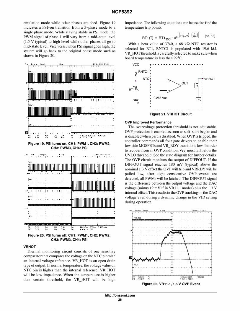
VRHOTThermal monitoring circuit consists of one sensitive
comparator that compares the voltage on the NTC pin withan internal voltage reference. VR_HOT is an open draintype of output. In normal temperature, the voltage value onNTC pin is higher than the internal reference, VR_HOTwill be low impedance. When the temperature is higherthan certain threshold, the VR_HOT will be high
impedance. The following equations canbe used to find thetemperature trip points.
RT1(T)= RT125C ⋅ eβ 1273+T− 1
298 (eq. 18)
With a beta value of 3740, a 68 kΩ NTC resistor isselected for RT1, RNTC1 is populated with 19.6 kΩ.VR_HOT threshold is carefully selected tomake surewhenboard temperature is less than 92C.
RNTC1
RT1
0
+
--
OUT
0.268 Vcc
VCC
0
NTC VRHOT
Figure 21. VRHOT Circuit
OVP Improved PerformanceThe overvoltage protection threshold is not adjustable.
OVP protection is enabled as soon as soft--start begins andis disabledwhen part is disabled.When OVP is tripped, thecontroller commands all four gate drivers to enable theirlow sideMOSFETs and VR_RDY transitions low. In orderto recover from anOVPcondition, VCCmust fall below theUVLO threshold. See the state diagram for further details.The OVP circuit monitors the output of DIFFOUT. If theDIFFOUT signal reaches 180 mV (typical) above thenominal 1.3 Voffset the OVPwill trip andVRRDYwill bepulled low, after eight consecutive OVP events aredetected, all PWMs will be latched. The DIFFOUT signalis the difference between the output voltage and the DACvoltage (minus 19 mV if in VR11.1 modes) plus the 1.3 Vinternal offset. This results in theOVP trackingon theDACvoltage even during a dynamic change in the VID settingduring operation.
Figure 22. VR11.1, 1.6 V OVP Event

NCP5392
http://onsemi.com29
Figure 23. AMD, 1.55 V OVP Event
Gate Driver and MOSFET SelectionON Semiconductor provides the NCP5359 as a
companion gate driver IC. The NCP5359 driver isoptimized to work with a range of MOSFETs commonlyused in CPU applications. The NCP5359 provides specialfunctionality including power saving mode operation andis required for high performance dynamic VID operation.Contact your local ON Semiconductor applicationsengineer for MOSFET recommendations.
Board Stackup and Board LayoutClose attention should be paid to the routing of the sense
traces and control lines that propagate away from thecontroller IC. Routing should follow the demo boardexample. For further information or layout review contactON Semiconductor.

NCP5392
http://onsemi.com30
SYSTEM TIMING DIAGRAM
Figure 24. Normal Startup
500 ms
500 ms
3.5 ms
VR_RDY
VSP--VSN
VID
DRVON
EN
UVLO
5 V (Controller)
1.5 ms
1 ms min
Valid VID
12 V (Gate Driver)
UVLO
Figure 25. Driver UVLO Limited Startup
500 ms
500 ms
3.5 ms
VR_RDY
VSP--VSN
VID
DRVON
EN
UVLO5 V (Controller)
POR
1 ms
1.5 ms
1 ms min
UVLO
Valid VID
12 V (Gate Driver)

NCP5392
http://onsemi.com31
Figure 26. OVP Shutdown
185 mVVSP = VID -- 19 mV
DRVON = High
VR_RDY
Diffout ~ 1.3 V 185 mV
1 2 3 4 5 6 7 8
1 2 3 4 5 6 7 8
Figure 27. Non--PSI Current Limit
VDRP
VR_RDY
DRVON
Ilimit + 1.3
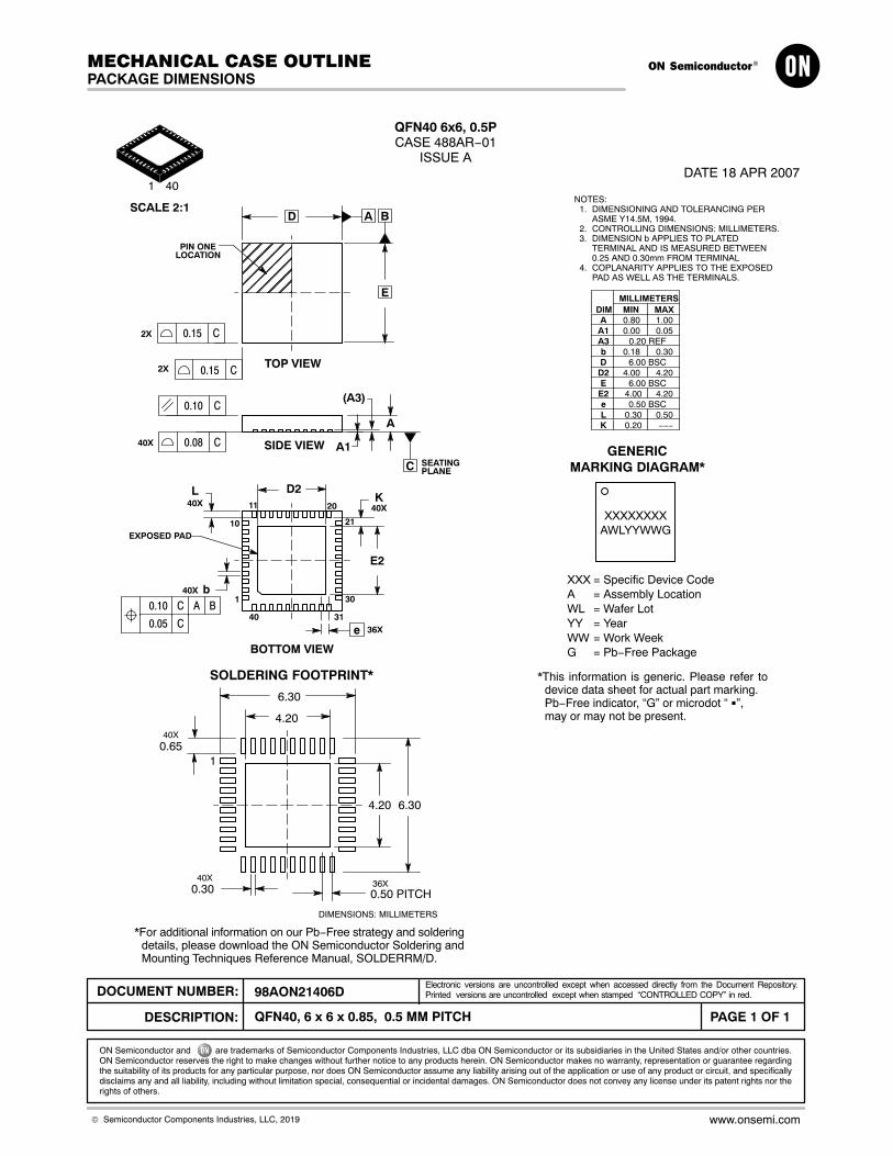
QFN40 6x6, 0.5PCASE 488AR−01
ISSUE ADATE 18 APR 2007
SCALE 2:1
SEATING
40X
K
0.15 C
(A3)
A
A1
D2
b1
11 20
21
40
2X
2X
E2
40X
10
30
40X
L40X
BOTTOM VIEW
EXPOSED PAD
TOP VIEW
SIDE VIEW
D A B
E
0.15 C
ÉÉÉÉÉÉÉÉÉÉÉÉÉÉÉÉ
PIN ONELOCATION
0.10 C
0.08 C
C
31
e
A0.10 BC
0.05 C
NOTES:1. DIMENSIONING AND TOLERANCING PER
ASME Y14.5M, 1994.2. CONTROLLING DIMENSIONS: MILLIMETERS.3. DIMENSION b APPLIES TO PLATED
TERMINAL AND IS MEASURED BETWEEN0.25 AND 0.30mm FROM TERMINAL
4. COPLANARITY APPLIES TO THE EXPOSEDPAD AS WELL AS THE TERMINALS.
DIM MIN MAXMILLIMETERS
A 0.80 1.00A1 0.00 0.05A3 0.20 REFb 0.18 0.30D 6.00 BSCD2 4.00 4.20E 6.00 BSC
4.20E2 4.00e 0.50 BSCL 0.30 0.50K 0.20 −−−
401
36X
*This information is generic. Please refer todevice data sheet for actual part marking.Pb−Free indicator, “G” or microdot “ �”,may or may not be present.
GENERICMARKING DIAGRAM*
XXX = Specific Device CodeA = Assembly LocationWL = Wafer LotYY = YearWW = Work WeekG = Pb−Free Package
XXXXXXXXAWLYYWWG
PLANE
DIMENSIONS: MILLIMETERS
0.50 PITCH
4.20
0.30
4.20
40X36X
0.6540X
6.30
6.30
*For additional information on our Pb−Free strategy and solderingdetails, please download the ON Semiconductor Soldering andMounting Techniques Reference Manual, SOLDERRM/D.
SOLDERING FOOTPRINT*
1
MECHANICAL CASE OUTLINE
PACKAGE DIMENSIONS
ON Semiconductor and are trademarks of Semiconductor Components Industries, LLC dba ON Semiconductor or its subsidiaries in the United States and/or other countries.ON Semiconductor reserves the right to make changes without further notice to any products herein. ON Semiconductor makes no warranty, representation or guarantee regardingthe suitability of its products for any particular purpose, nor does ON Semiconductor assume any liability arising out of the application or use of any product or circuit, and specificallydisclaims any and all liability, including without limitation special, consequential or incidental damages. ON Semiconductor does not convey any license under its patent rights nor therights of others.
98AON21406DDOCUMENT NUMBER:
DESCRIPTION:
Electronic versions are uncontrolled except when accessed directly from the Document Repository.Printed versions are uncontrolled except when stamped “CONTROLLED COPY” in red.
PAGE 1 OF 1QFN40, 6 x 6 x 0.85, 0.5 MM PITCH
© Semiconductor Components Industries, LLC, 2019 www.onsemi.com

onsemi, , and other names, marks, and brands are registered and/or common law trademarks of Semiconductor Components Industries, LLC dba “onsemi” or its affiliatesand/or subsidiaries in the United States and/or other countries. onsemi owns the rights to a number of patents, trademarks, copyrights, trade secrets, and other intellectual property.A listing of onsemi’s product/patent coverage may be accessed at www.onsemi.com/site/pdf/Patent−Marking.pdf. onsemi reserves the right to make changes at any time to anyproducts or information herein, without notice. The information herein is provided “as−is” and onsemi makes no warranty, representation or guarantee regarding the accuracy of theinformation, product features, availability, functionality, or suitability of its products for any particular purpose, nor does onsemi assume any liability arising out of the application or useof any product or circuit, and specifically disclaims any and all liability, including without limitation special, consequential or incidental damages. Buyer is responsible for its productsand applications using onsemi products, including compliance with all laws, regulations and safety requirements or standards, regardless of any support or applications informationprovided by onsemi. “Typical” parameters which may be provided in onsemi data sheets and/or specifications can and do vary in different applications and actual performance mayvary over time. All operating parameters, including “Typicals” must be validated for each customer application by customer’s technical experts. onsemi does not convey any licenseunder any of its intellectual property rights nor the rights of others. onsemi products are not designed, intended, or authorized for use as a critical component in life support systemsor any FDA Class 3 medical devices or medical devices with a same or similar classification in a foreign jurisdiction or any devices intended for implantation in the human body. ShouldBuyer purchase or use onsemi products for any such unintended or unauthorized application, Buyer shall indemnify and hold onsemi and its officers, employees, subsidiaries, affiliates,and distributors harmless against all claims, costs, damages, and expenses, and reasonable attorney fees arising out of, directly or indirectly, any claim of personal injury or deathassociated with such unintended or unauthorized use, even if such claim alleges that onsemi was negligent regarding the design or manufacture of the part. onsemi is an EqualOpportunity/Affirmative Action Employer. This literature is subject to all applicable copyright laws and is not for resale in any manner.
PUBLICATION ORDERING INFORMATIONTECHNICAL SUPPORTNorth American Technical Support:Voice Mail: 1 800−282−9855 Toll Free USA/CanadaPhone: 011 421 33 790 2910
LITERATURE FULFILLMENT:Email Requests to: [email protected]
onsemi Website: www.onsemi.com
Europe, Middle East and Africa Technical Support:Phone: 00421 33 790 2910For additional information, please contact your local Sales Representative
◊


