NCP1910 - High Performance Combo Controller for ATX Power ...
37
© Semiconductor Components Industries, LLC, 2014 June, 2014 - Rev. 2 1 Publication Order Number: NCP1910/D NCP1910 High Performance Combo Controller for ATX Power Supplies Housed in a SO-24WB package, the NCP1910 combines a state-of-the-art circuitry aimed to powering next generation of ATX or flat TVs converters. With a 65 or 100 kHz Continuous Conduction Mode Power Factor Controller and a LLC controller hosting a high-voltage driver, the NCP1910 is ready to power 85+ types of offline power supplies. To satisfy stringent efficiency considerations, the PFC circuit implements an adjustable frequency fold back to reduce switching losses as the load is going light. To cope with all the signal sequencing required by the ATX and flat TVs specifications, the controller includes several dedicated pins enabling handshake between the secondary and the primary sides. These signals include a power-good line but also a control pin which turns the controller on and off via an opto coupler. Safety-wise, a second OVP input offers the necessary redundancy in case the main feedback network would drift away. Finally, a fast fault input immediately reacts in presence of an over current condition by triggering an auto-recovery soft-start sequence. Features • Fixed-Frequency 65 or 100 kHz CCM Power Factor Controller • Average Current-Mode Control for Low Line Distortion • Dynamic Response Enhancer Reduces Bulk Undershoot • Independent Over Voltage Protection Sensing Pin with Latch-off Capability • Adjustable Frequency Fold Back Improves Light Load Efficiency • Adjustable Line Brown-Out Protection with 50 ms Delay to Help Meeting Hold-up Time Specifications • Programmable Over current Threshold Leads to an Optimized Sensing Resistor • ±1 A peak Current Drive Capability • LLC Controller Operates from 25 kHz to 500 kHz • On Board 600 V High-Voltage Drivers • 1 A/0.5 A Sink/Source Capability • Minimum Frequency Precision Down to ±3% Over Temperature Range • Internally Fixed Dead-Time Value of 300 ns • Adjustable Soft-Start Sequence • Fast Fault Input with Soft-Start Trigger for Immediate Auto-recovery Protection • On /Off Control Pin for Secondary-Based Remote Control • On-Board 5 V Reference Voltage for Precise Thresholds/Hysteresis Adjustments • Power Good Output Management Signal • A Version with Dual Ground Pinout (No Skip), B Version with Single Ground and Skip Operation for the LLC Controller • 20 V Operation • These are Pb-Free Devices Typical Applications • Multi Output ATX Power Supplies (A version) • Flat TVs Power Supplies (B version) MARKING DIAGRAM SO-24WB Less Pin 21 DW SUFFIX CASE 752AB http://onsemi.com See detailed ordering and shipping information in the package dimensions section on page 35 of this data sheet. ORDERING INFORMATION NCP1910XXX AWLYYWWG 1 XXXXX = Specific Device Code A = Assembly Location WL = Wafer Lot YY = Year WW = Work Week G = Pb-Free Package
-
Upload
duongkhuong -
Category
Documents
-
view
232 -
download
0
Transcript of NCP1910 - High Performance Combo Controller for ATX Power ...

© Semiconductor Components Industries, LLC, 2014
June, 2014 − Rev. 21 Publication Order Number:
NCP1910/D
NCP1910
High Performance ComboController for ATX PowerSupplies
Housed in a SO−24WB package, the NCP1910 combinesa state-of-the-art circuitry aimed to powering next generation of ATXor flat TVs converters. With a 65 or 100 kHz Continuous ConductionMode Power Factor Controller and a LLC controller hostinga high-voltage driver, the NCP1910 is ready to power 85+ types ofoffline power supplies. To satisfy stringent efficiency considerations,the PFC circuit implements an adjustable frequency fold back toreduce switching losses as the load is going light. To cope with all thesignal sequencing required by the ATX and flat TVs specifications, thecontroller includes several dedicated pins enabling handshakebetween the secondary and the primary sides. These signals includea power-good line but also a control pin which turns the controller onand off via an opto coupler. Safety-wise, a second OVP input offers thenecessary redundancy in case the main feedback network would driftaway. Finally, a fast fault input immediately reacts in presence of anover current condition by triggering an auto-recovery soft-startsequence.
Features• Fixed-Frequency 65 or 100 kHz CCM Power Factor Controller
• Average Current-Mode Control for Low Line Distortion
• Dynamic Response Enhancer Reduces Bulk Undershoot
• Independent Over Voltage Protection Sensing Pin with Latch-offCapability
• Adjustable Frequency Fold Back Improves Light Load Efficiency
• Adjustable Line Brown-Out Protection with 50 ms Delay to HelpMeeting Hold-up Time Specifications
• Programmable Over current Threshold Leads to an OptimizedSensing Resistor
• ±1 A peak Current Drive Capability
• LLC Controller Operates from 25 kHz to 500 kHz
• On Board 600 V High-Voltage Drivers
• 1 A/0.5 A Sink/Source Capability
• Minimum Frequency Precision Down to ±3% OverTemperature Range
• Internally Fixed Dead-Time Value of 300 ns
• Adjustable Soft-Start Sequence
• Fast Fault Input with Soft-Start Trigger for ImmediateAuto-recovery Protection
• On/Off Control Pin for Secondary-Based RemoteControl
• On-Board 5 V Reference Voltage for PreciseThresholds/Hysteresis Adjustments
• Power Good Output Management Signal
• A Version with Dual Ground Pinout (No Skip),B Version with Single Ground and Skip Operation forthe LLC Controller
• 20 V Operation
• These are Pb-Free Devices
Typical Applications• Multi Output ATX Power Supplies (A version)
• Flat TVs Power Supplies (B version)
MARKING DIAGRAM
SO−24WB Less Pin 21DW SUFFIX
CASE 752AB
http://onsemi.com
See detailed ordering and shipping information in the packagedimensions section on page 35 of this data sheet.
ORDERING INFORMATION
NCP1910XXXAWLYYWWG
1
XXXXX = Specific Device CodeA = Assembly LocationWL = Wafer LotYY = YearWW = Work WeekG = Pb−Free Package

NCP1910
http://onsemi.com2
Figure 1. Pin Connections
GND/PGNDOVP2DRVPG adj.VCCVrefMLBO adj.
ON/OFFBridgePG outMURtVbootSS
Skip/AGNDFBCS/FFVCTRL
1 24
FoldLBOCSVM
PIN DESCRIPTION
Pin No Pin Name Function Pin Description
1 SS Soft-Start A capacitor to ground sets the LLC soft-start duration
2 Rt The LLC Feedback Pin A resistive arrangement sets the maximum and minimumswitching frequencies with opto coupler-based feedbackcapabilities.
3 PG out The Open-Collector Power Good Signal
This pin is low when Vbulk is ok, opens when Vbulk passesbelow a level adjusted by PGadj pin.
4 on/off Remote Control When pulled low, the circuit operates: the PFC starts first andonce FB is in regulation, the LLC is authorized to work. Whenleft open, the controller is in idle mode.
5 BO adj. Brown-Out Adjustment This pin sets the on and off levels for the PFC powering theLLC converter
6 Vref The 5 V Reference Pin This pin delivers a stable voltage for threshold adjustments
7 PG adj. The Power Good Trip Level From the Vref pin, a dc level sets the trip point for the PFCbulk voltage at which the PG out signal is down.
8 OVP2 Redundant OVP A fully latched OVP monitoring the PFC bulk independentlyfrom FB pin.
9 FB PFC Feedback Monitors the boost bulk voltage and regulates it. It also servesas a quick auto-recovery OVP
10 VCTRL PFC Error Amplifier Output PFC error amplifier compensation pin
11 VM PFC Current Amplifier Output A resistor to ground sets the maximum power level
12 LBO PFC Line Input Voltage Sensing Line feed forward and PFC brown-out
13 Fold PFC Fold Back This pin selects the power level at which the frequency startsto reduce gradually.
14 CS PFC Current Sense This pin senses the inductor current and also programs themaximum sense voltage excursion
15 CS/FF Fast-Fault Input When pulled above 1 V, the LLC stops and re-starts via a fullsoft-start sequence.
16 Skip/AGND Skip (B)/AGND (A) This pin is either used as the analog GND for the signal circuit(A) or for skip operation (B).
17 GND/PGND GND (B)/PGND (A) The controller ground for the driving loop (A) or the lumpground pin for all circuits (B)
18 DRV PFC Drive Signal The driving signal to the PFC power MOSFET
19 VCC The Controller Supply The power supply pin for the controller, 20 V max.
20 ML Lower-Side MOSFET Drive signal for the lower side half-bridge MOSFET
22 Bridge Half-Bridge This pin connects to the LLC half-bridge
23 MU Upper-Side MOSFET Drive signal for the upper side half-bridge MOSFET
24 Vboot Bootstrapped Vcc The bootstrapped VCC for the floating driver

NCP1910
http://onsemi.com3
*It
is r
ecom
men
ded
to s
epar
ate
the
trac
es o
f po
wer
gro
und
and
anal
og g
roun
d. T
he p
ower
gro
und
(pin
17)
for
driv
ing
loop
(P
FC
DR
V a
nd L
LC M
L) is
conn
ecte
d to
the
PF
C M
OS
FE
T d
irect
ly. T
he a
nalo
g gr
ound
for
adju
stm
ent c
ompo
nent
s is
rou
ted
toge
ther
firs
t and
then
con
nect
ed to
the
anal
og g
roun
dpi
n (p
in 1
6) a
nd th
e P
FC
sen
se r
esis
tor
dire
ctly
.
Figure 2. Typical Application Schematic in A Version
M1
M2
C14
L2D
6
D9
T1
C4
Vo
ut
R11
R30
U1
C7
U2BR
10
R18
. .
.
R9
R17
R8
R16
C3
Ove
r C
urre
ntC
15
R29
D12
D11
C13
R28
1 2 3 4 5 86 7 9
10
1314151617181920
11 12
222324
U10
0
C12
R22
R12
U2A
U3A
C10
0.1u
Bul
k
12 V
aux
.
on/o
ffF
B
Vcc
R21
Vre
f
Pow
erG
ood
C6
0.1u
R14
R15
PG
adj
.R
13
BO
leve
l
R31
0.1
D4
D8
D3
D7
C5
D2
C1
L1
R19 10
D10
R20
10k
R1
3.5M
R2
1.5M
R32
3.6kR4
2.2M
R5
3.5M
Inpu
tLi
ne
D5
D1
R23
120k
C8
0.22
uC2
R24
24k
R3
1.5M
R7
2.2M
R26
24k
C9
1u
R25
24k
R27
39k
C11
1n
R33
1.2k
R6
Vre
f
X2
PA
D2
X3
V33
V32
C16
0.1u
R34
8.4k
C17 1n
(*)(*
)
Q1
R35
300
C18
1n

NCP1910
http://onsemi.com4
*It i
s re
com
men
ded
to s
epar
ate
the
trac
es o
f pow
er g
roun
d an
d an
alog
gro
und.
The
ana
log
grou
nd tr
aces
for
adju
stm
ent c
ompo
nent
s ar
e ro
uted
toge
ther
firs
t and
then
conn
ecte
d to
the
grou
nd p
in (
pin
17).
The
pow
er g
roun
d fo
r dr
ivin
g lo
op (
PF
C D
RV
and
LLC
ML)
is c
onne
cted
from
gro
und
pin
(pin
17)
to th
e P
FC
sen
se r
esis
tor
dire
ctly
and
as s
hort
as
poss
ible
.
Figure 3. Typical Application Schematic in B Version
M1
M2
C14
L2D
6
D9
T1
C4
Vo
ut
R11
R30
U1
C7
U2B
R10
R18
. .
.
R9
R17
R8
R16
C3
Ove
r C
urre
ntC
15
R29
D12
D11
C13
R28
1 2 3 4 5 86 7 9 10
1314151617181920
11 12
21222324
U10
0
C12
R22
R12
U2A
U3A
C10
0.1u
Bul
k
12 V
aux
.
on/o
ff
FB
Vcc
R21
Vre
f
Pow
erG
ood
C6
0.1u
R14
R15
PG
adj
.R
13
BO
leve
l
R31
0.1
D4
D8
D3
D7
C5
D2
C1
L1
R19
10
D10
R20
10k
R1
3.5M
R2
1.5M
R32
3.6kR4
2.2M
R5
3.5M
Inpu
tLi
ne
D5
D1
R23
120k
C8
0.22
u
C2
R24
24k
R3
1.5M
R7
2.2M
R26
24k
C9
1u
R25
24k
R27
39k
C11
1n
R33
1.2k
R6
Vre
f
X2
PA
D2
X3
V33
V32
C16
0.1u
R34
8.4k
C17
1n
(*)(*
)
Q1
R35
300
C18
1n
R36
C19
skip

NCP1910
http://onsemi.com5
+
−
+
−
VOVPVUVP
105% Vpref
8% Vpref
PFC_OPL
+
−
OVP2
FB
95% Vpref
+
−
VLD
Vpref
VCTRL
OTA
Vctrl(min)
A
BMultiplier
LBO
CS
VDD
VLBO^2
“1” BO NOTOK,“0” BOK
A
BA/B
ICS
AB
Vctrl−Vctrl(min)
ICS x VLBO^2
+
−
+
−
ICS x VLBO > 275 uA
ICS > 200 uA
ICS SU
M 2
K1
K2
PFC_OL
VM
+ −
“0” / “1”Vpref / 10%Vpref
S
R
+
−
Vpref
PFC_OVPPFC_OL
TSD
VLBO^2
VDD
IVLD
DynamicResponseEnhancer
“1” = UVP, “0” ok
Closedif “1”
“1” OVP, “0” = ok
Vfold
ICS
Vdd
Oscillator section
ICt(min)
DRV
Vcc
foldback
PFC drive signal
OnoffUVLO
Latch
RFBpull down
“1” = OPL
“1” = OCP
PFC_UVP
The “PFC_OK” toggles high when:− VLD is low− PFC issues a driving pulseThe “PFC_OK” toggles low when:− Vctrl stays out of window [Vctrl,min toVctrl,max] > 1 sec− at this point, the latch is reset and the“PFC_OK” output goes low.
“1” = below 5% reg“0” ok
Auto−recovery internal OVP
+
−VOVP2
107% Vpref “1” OVP2, “0” = okLatched adjustable OVP2
PFC_OVP2latched
Vctrl
+
−
Vctrl(min) − 0.1 V
Vctrl
+
−
1 secdelay
If PFC issues an abnormalsituation, then latch off
Grand Reset
PFC_OK
PFC_OK
S
R
PFC_OK
Grand Reset
PFC_SKIP(0.6 V clampvoltage isactivated.)
VLBOPFC_BO+
−ILBO
VLBOT
20 us filter
Latch
PFC_BO
PFC_SKIP
+
−
Vctrl(max)PFCflag
ICt
Vfold(max)
Ict(fold)
S
RQQ
PFC_OVP
Grand Reset
PFC_OCP
PFC_OPL
GrandReset
“1” open“0” close
PFC_abnormallatched
PFC_BO
PFC_BO
PFC_BO
PFC_BO
+
−
“1” = FB > Vpref
S
RQQ
Grand ResetPFC_BO
Figure 4. Internal PFC Block Diagram
ICS � VLBO2
4(Vctrl � Vctrl(min))
BO delay

NCP1910
http://onsemi.com6
Rt
Vref
PG adj
PG out
CS/FF
on/off
BO adj
Vcc
management
UVLO
Hi sideLevel
shifter
Vrt
+
-
S
R
Q
QClk
D
Vboot
Mupper
Bridge
Vcc
Mlower
GND_LLC
delay
Dead time
A
B
B
A
PFC_FB
"1" BONOT OK
20 ms delay
tdel1
"1" enables LLC"0" LLC is locked
GrandReset
SS
+
-
SS_RST
+
-
VCS1
+
-
VCS2
UVLO
Vdd
Vref
LLC_BO
GrandReset
S
R
Q
Q
Grand Reset
Onoff
UVLO
PFC_BO
Grand Reset
Grand Reset
GrandReset
R
Latch
Latch
Vdd
Rpull upon_off
on/off"1" controller is off"0" controller is on
GND
Prop. delaymatching
PFC_UVP
PFC_OK"1" is ok"0" notok
5 ms delay
tdel2
R
"1" after reset"0" when PG outdrops after 5 ms
PFC_OVP2
LLC_BO
Latch
Pulse
Trigger
S
R
CLKQ
QN
S
R
Q
Q
Skip/GND_PFC
+
-Vskip
Skip: B version only
ThermalShut Down
TSDTSD"1" TSD is on"0" TSD is off
GrandReset
"1" PGNOT OK
+
-
+
-
tBOK
tBONOTOK
LLC_BO
LLC_PG
S
R
LLC_PG
Grand Reset
Figure 5. Internal LLC Block Diagram

NCP1910
http://onsemi.com7
MAXIMUM RATINGS
Symbol Rating Value Unit
VBridge Continuous High Voltage Bridge Pin, Pin 22 −1 to 600 V
VBOOT–VBridge Floating Supply Voltage, Pin 24−22 −0.3 to 20 V
VMU, VDRV High Side Output Voltage, Pin 23 VBRIDGE − 0.3 toVBOOT + 0.3
V
VML Low Side Output Voltage, Pin 18, 20 −0.3 to VCC + 0.3 V
dVBridge/dt Allowable Output Slew Rate on the Bridge Pin, Pin 22 50 V/ns
VCC Power Supply Voltage, Pin 19 20 V
Pin Voltage, All Pins (except pin 2, 6, 18−24, GND) −0.3 to 10 V
RθJA Thermal Resistance Junction-to-Air50 mm2, 1 oz650 mm2, 1 oz
8065
°C/W
Storage Temperature Range −60 to + 150 °C
ESD Capability, Human Body Model (All pins except VCC and HV) 2 kV
ESD Capability, Machine Model 200 V
VCC Power Supply Voltage, Pin 19 20 V
Pin Voltage, All Pins (except pin 2, 6, 18 ~ 24, GND) −0.3 to 10 V
VRt Rt Pin Voltage −0.3 to 5 V
Vref_out Vref Pin Voltage −0.3 to 7 V
IMAX Pin Current on Pin 10, 12, and 13 0.5 mA
IPGout Pin Current on Pin 3 5 mA
Stresses exceeding those listed in the Maximum Ratings table may damage the device. If any of these limits are exceeded, device functionalityshould not be assumed, damage may occur and reliability may be affected.1. This device(s) contains ESD protection and exceeds the following tests:
Human Body Model 2000 V per JEDEC Standard JESD22−A114EMachine Model 200 V per JEDEC Standard JESD22−A115−A
2. This device contains latch-up protection and exceeds 100 mA per JEDEC Standard JESD78.
ELECTRICAL CHARACTERISTICS (For typical values TJ = 25°C, for min/max values TJ = −40°C to +125°C, Max TJ = 150°C, VCC = 12 V unless otherwise noted)
Symbol Rating Pin Min Typ Max Unit
COMMON TO BOTH CONTROLLERS
SUPPLY SECTION
VCC(on) Turn-On Threshold Level, VCC Going Up 19 9.4 10.4 11.4 V
VCC(min) Minimum Operating Voltage after Turn-On 19 8 9 10 V
VCC(Hys) Hysteresis between VCC(on) and VCC(min) 19 1.2 − − V
VBoot(on) Startup Voltage on the Floating Section 24,22 7.8 8.8 9.8 V
VBoot(min) Cutoff Voltage on the Floating Section 24,22 7 8 9 V
Istartup Startup Current, VCC < VCC(on) 19 − − 100 �A
ICC1 PFC Consumption Alone, DRV Pin Unloaded, On/Off Pin Grounded,LLC Off
• 65 kHz Version• 100 kHz Version
19
−−
5.15.3
6.46.54
mA
Product parametric performance is indicated in the Electrical Characteristics for the listed test conditions, unless otherwise noted. Productperformance may not be indicated by the Electrical Characteristics if operated under different conditions.3. In normal operation, when the power supply is un-plugged, the bulk voltage goes down. At a first crossed level, the PG pin opens. Later,
when the bulk crosses a second level, the LLC turns off. There is no timing link between these events, except the bulk capacitor dischargeslope. However, if for an unknown reason the PFC is disabled (fault, short-circuit), the PG pin immediately opens and if sufficient voltageis still present on the bulk (e.g. in high line condition), the LLC will be disabled after a typical time of 5 ms.
4. Guaranteed by design.

NCP1910
http://onsemi.com8
ELECTRICAL CHARACTERISTICS (continued)(For typical values TJ = 25°C, for min/max values TJ = −40°C to +125°C, Max TJ = 150°C, VCC = 12 V unless otherwise noted)
Symbol UnitMaxTypMinPinRating
COMMON TO BOTH CONTROLLERS
SUPPLY SECTION
ICC2 PFC Consumption Alone, DRV Pin Loaded by 1 nF, On/Off Pin Grounded, LLC Off
• 65 kHz Version• 100 kHz Version
19
−−
5.96.4
7.47.9
mA
ICC4 IC Consumption, Both PFC & LLC DRV Pin Unloaded, Rt = 70 k� (LLC FSW = 25 kHz)
• 65 kHz Version• 100 kHz Version
19
−−
5.96.0
7.27.3
mA
ICC5 IC Consumption, Both PFC & LLC DRV Pin Loaded by 1 nF, Rt = 70 k� (LLC FSW = 25 kHz)
• 65 kHz Version• 100 kHz Version
19
−−
6.97.4
8.69.1
mA
ICC6 IC Consumption in Fault Mode from Vboot (Drivers Disabled, Vboot > Vboot(min))
19 − 64 300 �A
ICC7 IC Consumption in OFF Mode from VCC (On/Off Pin is Open) 19 − − 950 �A
REFERENCE VOLTAGE
Vref-out Reference Voltage for External Threshold Setting @ Iout = 5 mA 6 4.75 5 5.25 V
Vref-out Reference Voltage for External Threshold Setting @ Iout = 5 mA – TJ = 25°C
6 4.9 5 5.1 V
VrefLineReg Vcc Rejection Capability, Iout = 5 mA − �VCC = 1 V – TJ = 25°C 6 − 0.01 5 mV
VrefLoadReg Reference Variation with Load Changes, 1 mA < Iref < 5 mA – TJ = 25°C
6 − 1.6 7 mV
Iref−out Maximum Output Current Capability 6 5 − − mA
NOTE: Maximum capacitance directly connected to VREF pin must be under 100 nF.
DELAY
tDEL1 Turn-On LLC Delay after PFC OK Signal is Asserted − 10 20 30 ms
tDEL2 Turn-Off LLC after Power Good Pin Goes Low (Note 3) − 2 5 8 ms
PROTECTIONS
RPull-up On/Off Pin Pull-Up Resistor 4 − 5 − k�
ton/off Propagation Delay from On to Off (ML & MU are Off) (Note 4) 4 − − 1 �s
Von Low Level Input Voltage on On/Off Pin (NCP1910 is Enabled) 4 − − 1 V
Voff High Level Input Voltage on On/Off Pin (NCP1910 is Disabled) 4 3 − − V
Vop Open Voltage on On/Off Pin 4 − 7 − V
IPG Maximum Power Good Pin Sink Current Capability 3 5 − − mA
VPG Power Good Saturation Voltage for IPG = 5 mA 3 − − 350 mV
IPGadj Input Bias Current, PGadj Pin 7 − 10 − nA
VPGadjH PG Comparator Hysteresis 7 − 100 − mV
TSD Temperature Shutdown (Note 4) − 140 − − °C
TSDhyste Temperature Hysteresis Shutdown − − 30 − °C
Product parametric performance is indicated in the Electrical Characteristics for the listed test conditions, unless otherwise noted. Productperformance may not be indicated by the Electrical Characteristics if operated under different conditions.3. In normal operation, when the power supply is un-plugged, the bulk voltage goes down. At a first crossed level, the PG pin opens. Later,
when the bulk crosses a second level, the LLC turns off. There is no timing link between these events, except the bulk capacitor dischargeslope. However, if for an unknown reason the PFC is disabled (fault, short-circuit), the PG pin immediately opens and if sufficient voltageis still present on the bulk (e.g. in high line condition), the LLC will be disabled after a typical time of 5 ms.
4. Guaranteed by design.

NCP1910
http://onsemi.com9
ELECTRICAL CHARACTERISTICS (continued)(For typical values TJ = 25°C, for min/max values TJ = −40°C to +125°C, Max TJ = 150°C, VCC = 12 V unless otherwise noted)
Symbol UnitMaxTypMinPinRating
POWER FACTOR CORRECTION
GATE DRIVE SECTION
RPOH Source Resistance @ IDRV = −100 mA 18 − 9 20 �
RPOL Sink Resistance @ IDRV = 100 mA 18 − 6.6 18 �
tPr Gate Drive Voltage Rise Time from 1.5 V to 10.5 V (CL = 1 nF) 18 − 60 − ns
tPf Gate Drive Voltage Fall Time from 10.5 V to 1.5 V (CL = 1 nF) 18 − 40 − ns
REGULATION BLOCK
VPREF PFC Voltage Reference − 2.425 2.5 2.575 V
IEA Error Amplifier Current Capability 10 − �30 − �A
GEA Error Amplifier Gain − 100 200 300 �S
IB Bias Current @ VFB = VPREF 9 0 − 0.3 �A
VCTRLVCTRL(max)VCTRL(min)�VCTRL
Maximum Control Voltage @ VFB = 2 VMinimum Control Voltage @ VFB = 3 V�VCTRL = VCTRL(max)−VCTRL(min)
101010
−−
2.7
3.60.63
−−
3.3
V
VOUTL / VPREF Ratio (VOUT Low Detect Threshold / VPREF) (Note 4) − 94 95 96 %
HOUTL / VPREF Ratio (VOUT Low Detect Hysteresis / VPREF) − − 0.5 − %
IVLD + IEA Source Current when (VOUT Low Detect) is Activated 10 190 230 260 �A
CURRENT SENSE
VS Current Sense Pin Offset Voltage, (ICS = 100 �A) 14 − 10 − mV
ICS(OCP) Over-Current Protection Threshold 14 185 200 215 �A
POWER LIMIT
ICSx VLBO Over Power Limitation Threshold − 215 275 335 �VA
ICS(OPL1)ICS(OPL2)
Over-Power Current Threshold (VLBO = 1.8 V, VM = 0 V)Over-Power Current Threshold (VLBO = 3.6 V, VM = 0 V)
− 11956
15375
18799
�A
PULSE WIDTH MODULATION
FPSW PFC Switching Frequency• 65 kHz Version• 100 kHz Version
185890
65100
72110
kHz
FPSW(fold) Minimum Switching Frequency (Vfold = 1.5 V, VCTRL = VCTRL(min) + 0.1 V)
• 65 kHz Version• 100 kHz Version
18
3433
3940
4346
kHz
DCPmax Maximum PFC Duty Cycle 18 − 97 − %
DCPmin Minimum PFC Duty Cycle 18 − − 0 %
VCTRL(fold) VCTRL Pin Voltage to Start Frequency Foldback (Vfold = 1.5 V) 10 1.8 2 2.2 V
VCTRL(foldend) VCTRL Pin Voltage as Frequency Foldback Reducing to the Minimum(FPSW = FPSW(fold), Vfold = 1.5 V)
10 1.4 1.6 1.8 V
Vfold(max) Maximum Internal Fold Voltage (Note 4) − 1.97 2 2.03 V
LINE BROWN-OUT DETECTION
VLBOT Line Brown-Out Voltage Threshold 12 0.96 1.00 1.04 V
ILBOH Line Brown-Out Hysteresis Current Source 12 6 7 8 �A
Product parametric performance is indicated in the Electrical Characteristics for the listed test conditions, unless otherwise noted. Productperformance may not be indicated by the Electrical Characteristics if operated under different conditions.3. In normal operation, when the power supply is un-plugged, the bulk voltage goes down. At a first crossed level, the PG pin opens. Later,
when the bulk crosses a second level, the LLC turns off. There is no timing link between these events, except the bulk capacitor dischargeslope. However, if for an unknown reason the PFC is disabled (fault, short-circuit), the PG pin immediately opens and if sufficient voltageis still present on the bulk (e.g. in high line condition), the LLC will be disabled after a typical time of 5 ms.
4. Guaranteed by design.

NCP1910
http://onsemi.com10
ELECTRICAL CHARACTERISTICS (continued)(For typical values TJ = 25°C, for min/max values TJ = −40°C to +125°C, Max TJ = 150°C, VCC = 12 V unless otherwise noted)
Symbol UnitMaxTypMinPinRating
POWER FACTOR CORRECTION
LINE BROWN-OUT DETECTION
tLBO(blank) Line Brown-Out Blanking Time − 25 50 75 ms
tLBO(window) Line Brown-Out Monitoring Window (Note 4) − 25 50 75 ms
VLBO(clamp) LBO Pin Clamped Voltage if VBO < VLBOT during tLBO(BLANK) (ILBO = 100 �A)
12 − 980 − mV
VLBOH Hysteresis (VLBOT – VLBO(clamp)) (Note 4) 12 10 35 60 mV
ILBO(clamp) Current Capability of LBO 12 100 − − �A
VLBO(PNP) LBO Pin Voltage when Clamped by the PNP Transistor (ILBO = 100 �A)
12 0.4 0.7 0.9 V
VLBO(PD) Pull Down VLBO Threshold 12 1.8 2 2.2 V
tLBO(Pdlimit) Pull Down VLBO Time Limitation − 4.5 5 6.1 ms
tPFCflag Time Delay to Confirm that VCTRL is the Maximum to Pull Down VLBO
− 2.5 5 7.5 ms
tLBO(Pdblank) Pull Down VLBO Blanking Time − 55 77 90 ms
CURRENT MODULATION
IM1
IM2
Multiplier Output Current (VCTRL = VCTRL(max) – 0.2 V, VLBO = 3.6 V, ICS = 50 �A)Multiplier Output Current (VCTRL = VCTRL(max) – 0.2 V, VLBO = 1.2 V, ICS = 150 �A)
11
11
46
15
58
19
72
24.5
�A
OVER-VOLTAGE PROTECTION
VOVP1 Internal Auto Recovery Over Voltage Threshold 9 2.536 2.615 2.694 V
VOVP1H Hysteresis of Internal Auto Recovery Over Voltage Threshold(Note 4)
9 − 44 60 mV
tOVP1 Propagation Delay (VFB = 108% VPREF) to Drive Low 9, 18 − 500 − ns
VOVP2 External Latched Over Voltage Threshold 8 2.595 2.675 2.755 V
KOVPH The Difference between VOVP2 and VOVP1 over VPREF ((VOVP2 − VOVP1)/VPREF)
− − 2 − %
tDELOVP2 External Latched OVP Integrating Filter Time Constant − − 20 − �s
Ib,OVP2 Input Bias Current, OVP2 8 − 10 − nA
UNDER-VOLTAGE PROTECTION
VUVP(on)/VPREF UVP Activate Threshold Ratio 9 4 8 12 %
VUVP(off)/VPREF UVP Deactivate Threshold Ratio 9 6 12 18 %
VUVP(H) UVP Lockout Hysteresis 9 − 4 − %
tUVP Propagation Delay (VFB < 8 % VPREF) to Drive Low 9−18 − 7 − �s
PFC ABNORMAL
tPFCabnormal PFC Abnormal Delay Time (VCTRL = VCTRL(max) or VCTRL = VCTRL(min) – 0.1 V)
− 1 1.5 2.1 sec
LLC CONTROL SECTION
OSCILLATOR
FLsw,min Minimum Switching Frequency, Rt = 70 k� on Rt Pin 2 24.25 25 25.75 kHz
Product parametric performance is indicated in the Electrical Characteristics for the listed test conditions, unless otherwise noted. Productperformance may not be indicated by the Electrical Characteristics if operated under different conditions.3. In normal operation, when the power supply is un-plugged, the bulk voltage goes down. At a first crossed level, the PG pin opens. Later,
when the bulk crosses a second level, the LLC turns off. There is no timing link between these events, except the bulk capacitor dischargeslope. However, if for an unknown reason the PFC is disabled (fault, short-circuit), the PG pin immediately opens and if sufficient voltageis still present on the bulk (e.g. in high line condition), the LLC will be disabled after a typical time of 5 ms.
4. Guaranteed by design.
NCP1910
http://onsemi.com11
ELECTRICAL CHARACTERISTICS (continued)(For typical values TJ = 25°C, for min/max values TJ = −40°C to +125°C, Max TJ = 150°C, VCC = 12 V unless otherwise noted)
Symbol UnitMaxTypMinPinRating
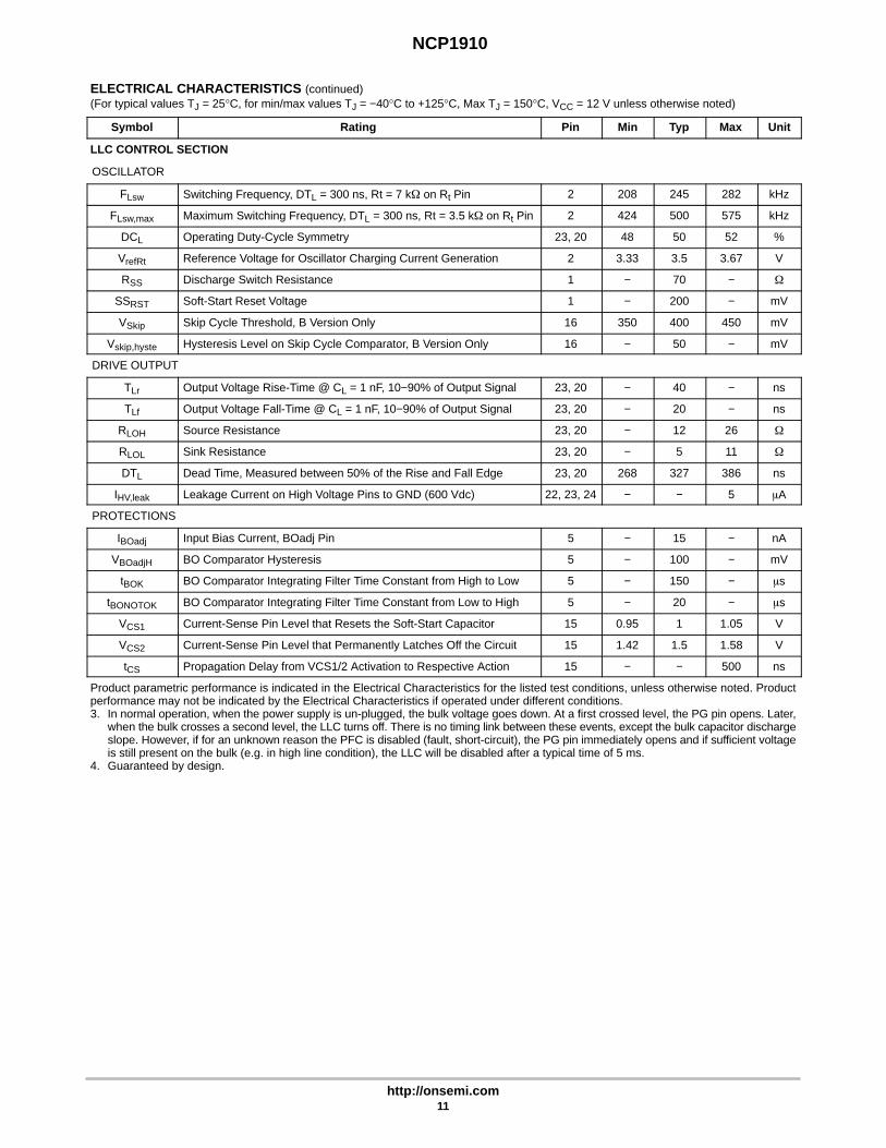
LLC CONTROL SECTION
OSCILLATOR
FLsw Switching Frequency, DTL = 300 ns, Rt = 7 k� on Rt Pin 2 208 245 282 kHz
FLsw,max Maximum Switching Frequency, DTL = 300 ns, Rt = 3.5 k� on Rt Pin 2 424 500 575 kHz
DCL Operating Duty-Cycle Symmetry 23, 20 48 50 52 %
VrefRt Reference Voltage for Oscillator Charging Current Generation 2 3.33 3.5 3.67 V
RSS Discharge Switch Resistance 1 − 70 − �
SSRST Soft-Start Reset Voltage 1 − 200 − mV
VSkip Skip Cycle Threshold, B Version Only 16 350 400 450 mV
Vskip,hyste Hysteresis Level on Skip Cycle Comparator, B Version Only 16 − 50 − mV
DRIVE OUTPUT
TLr Output Voltage Rise-Time @ CL = 1 nF, 10−90% of Output Signal 23, 20 − 40 − ns
TLf Output Voltage Fall-Time @ CL = 1 nF, 10−90% of Output Signal 23, 20 − 20 − ns
RLOH Source Resistance 23, 20 − 12 26 �
RLOL Sink Resistance 23, 20 − 5 11 �
DTL Dead Time, Measured between 50% of the Rise and Fall Edge 23, 20 268 327 386 ns
IHV,leak Leakage Current on High Voltage Pins to GND (600 Vdc) 22, 23, 24 − − 5 �A
PROTECTIONS
IBOadj Input Bias Current, BOadj Pin 5 − 15 − nA
VBOadjH BO Comparator Hysteresis 5 − 100 − mV
tBOK BO Comparator Integrating Filter Time Constant from High to Low 5 − 150 − �s
tBONOTOK BO Comparator Integrating Filter Time Constant from Low to High 5 − 20 − �s
VCS1 Current-Sense Pin Level that Resets the Soft-Start Capacitor 15 0.95 1 1.05 V
VCS2 Current-Sense Pin Level that Permanently Latches Off the Circuit 15 1.42 1.5 1.58 V
tCS Propagation Delay from VCS1/2 Activation to Respective Action 15 − − 500 ns
Product parametric performance is indicated in the Electrical Characteristics for the listed test conditions, unless otherwise noted. Productperformance may not be indicated by the Electrical Characteristics if operated under different conditions.3. In normal operation, when the power supply is un-plugged, the bulk voltage goes down. At a first crossed level, the PG pin opens. Later,
when the bulk crosses a second level, the LLC turns off. There is no timing link between these events, except the bulk capacitor dischargeslope. However, if for an unknown reason the PFC is disabled (fault, short-circuit), the PG pin immediately opens and if sufficient voltageis still present on the bulk (e.g. in high line condition), the LLC will be disabled after a typical time of 5 ms.
4. Guaranteed by design.

NCP1910
http://onsemi.com12
TYPICAL CHARACTERISTICS
8
8.5
9
9.5
10
10.5
11
−50 −25 0 25 50 75 100 125
VC
C(o
n) A
ND
VC
C(m
in) (
V)
Figure 6. VCC(on) and VCC(min) vs. Temperature
TEMPERATURE (°C)
VCC(on)
VCC(min)
7
7.5
8
8.5
9
9.5
10
−50 −25 0 25 50 75 100 125
TEMPERATURE (°C)
Vbo
ot(o
n) A
ND
Vbo
ot(m
in) (
V)
Figure 7. Vboot(on) and Vboot(min) vs.Temperature
Vboot(on)
Vboot(min)
0
25
50
75
100
−50 −25 0 25 50 75 100 125
I sta
rtup
(�A
)
TEMPERATURE (°C)
Figure 8. Istartup vs. Temperature
550
650
750
850
950
−50 −25 0 25 50 75 100 125
TEMPERATURE (°C)
Figure 9. ICC7 vs. Temperature
I CC
7 (�
A)
4.75
4.85
4.95
5.05
5.15
5.25
−50 −25 0 25 50 75 100 125
Vre
f−ou
t (V
)
Figure 10. Vref-out vs. TemperatureTEMPERATURE (°C)
4.987
4.988
4.989
4.99
0 1 2 3 4 5 6
Vre
f−ou
t @ 2
5°C
(V
)
TEMPERATURE (°C)Figure 11. Vref-out @ 25�C vs. Iref-out
NCP1910
http://onsemi.com13
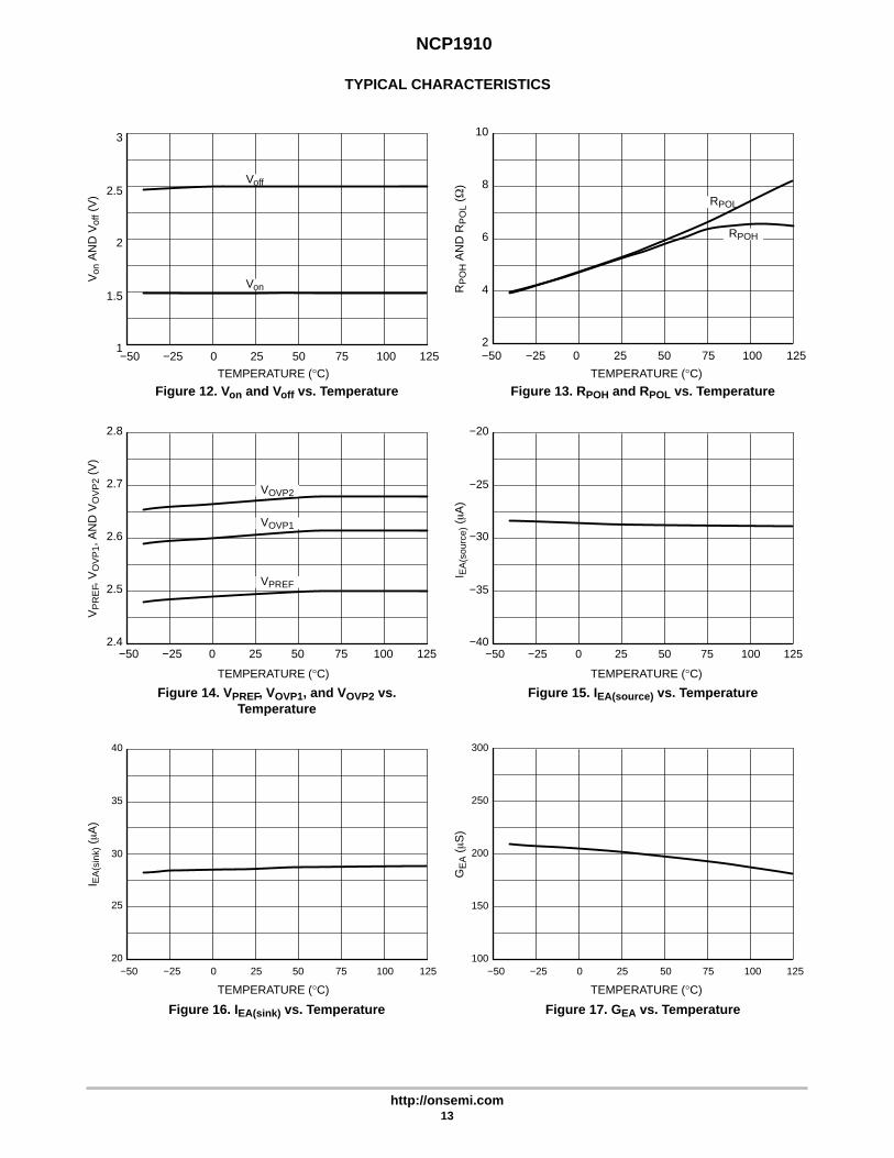
TYPICAL CHARACTERISTICS
1
1.5
2
2.5
3
−50 −25 0 25 50 75 100 125
Von
AN
D V
off (
V)
TEMPERATURE (°C)
Figure 12. Von and Voff vs. Temperature
Von
Voff
2
4
6
8
10
−50 −25 0 25 50 75 100 125
TEMPERATURE (°C)
RP
OH
AN
D R
PO
L (�
)
Figure 13. RPOH and RPOL vs. Temperature
RPOH
RPOL
2.4
2.5
2.6
2.7
2.8
−50 −25 0 25 50 75 100 125
VP
RE
F, V
OV
P1,
AN
D V
OV
P2
(V)
TEMPERATURE (°C)
Figure 14. VPREF, VOVP1, and VOVP2 vs.Temperature
VOVP2
VOVP1
VPREF
−40
−35
−30
−25
−20
−50 −25 0 25 50 75 100 125
I EA
(sou
rce)
(�A
)
TEMPERATURE (°C)
Figure 15. IEA(source) vs. Temperature
20
25
30
35
40
−50 −25 0 25 50 75 100 125
I EA
(sin
k) (�A
)
TEMPERATURE (°C)
Figure 16. IEA(sink) vs. Temperature
100
150
200
250
300
−50 −25 0 25 50 75 100 125
TEMPERATURE (°C)
GE
A (�S
)
Figure 17. GEA vs. Temperature

NCP1910
http://onsemi.com14
TYPICAL CHARACTERISTICS
3.3
3.4
3.5
3.6
3.7
3.8
3.9
−50 −25 0 25 50 75 100 125
TEMPERATURE (°C)
VC
TR
(max
) (V
)
Figure 18. VCTRL(max) vs. Temperature
2.7
2.8
2.9
3
3.1
3.2
3.3
−50 −25 0 25 50 75 100 125
�V
CT
R (
V)
TEMPERATURE (°C)
Figure 19. �VCTRL vs. Temperature
190
200
210
220
230
240
250
260
−50 −25 0 25 50 75 100 125
TEMPERATURE (°C)
I VLD
+ I E
A (�A
)
Figure 20. IVLD+IEA vs. Temperature
185
190
195
200
205
210
215
−50 −25 0 25 50 75 100 125
TEMPERATURE (°C)
I CS
(OC
P) (�A
)
Figure 21. ICS(OCP) vs. Temperature
120
130
140
150
160
170
180
190
−50 −25 0 25 50 75 100 125
TEMPERATURE (°C)
I CS
(OP
L1) (�A
)
Figure 22. ICS(OPL1) vs. Temperature
55
65
75
85
95
−50 −25 0 25 50 75 100 125
TEMPERATURE (°C)
I CS
(OP
L2) (�A
)
Figure 23. ICS(OPL2) vs. Temperature
NCP1910
http://onsemi.com15
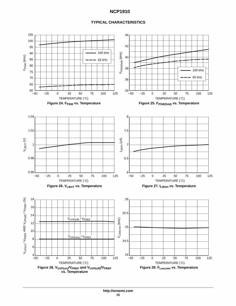
TYPICAL CHARACTERISTICS
60
65
70
75
80
85
90
95
−50 −25 0 25 50 75 100 125
TEMPERATURE (°C)
FP
SW
(kH
z)
Figure 24. FPSW vs. Temperature
34
36
38
40
42
44
−50 −25 0 25 50 75 100 125
FP
SW
(fol
d) (
kHz)
TEMPERATURE (°C)
Figure 25. FPSW(fold) vs. Temperature
0.96
0.98
1
1.02
1.04
−50 −25 0 25 50 75 100 125
VLB
OT (
V)
TEMPERATURE (°C)
Figure 26. VLBOT vs. Temperature
6
6.5
7
7.5
8
−50 −25 0 25 50 75 100 125
I LB
OH
(�A
)
TEMPERATURE (°C)
Figure 27. ILBOH vs. Temperature
4
6
8
10
12
14
16
18
−50 −25 0 25 50 75 100 125
VU
V(o
n) /
VP
RE
F A
ND
VU
P(o
ff) /
VP
RE
F (
%)
TEMPERATURE (°C)
Figure 28. VUVP(on)/VPREF and VUVP(off)/VPREFvs. Temperature
VUVP(on) / VPREF
VUVP(off) / VPREF
24
24.5
25
25.5
26
−50 −25 0 25 50 75 100 125
FLS
W,m
in (
kHz)
TEMPERATURE (°C)
Figure 29. FLsw,min vs. Temperature
100 kHz
65 kHz
100
105
100 kHz
65 kHz

NCP1910
http://onsemi.com16
TYPICAL CHARACTERISTICS
210
220
230
240
250
260
270
280
−50 −25 0 25 50 75 100 125
FLS
W (
kHz)
TEMPERATURE (°C)
Figure 30. FLsw vs. Temperature
425
450
475
500
525
−50 −25 0 25 50 75 100 125
FLS
W,m
ax (
kHz)
TEMPERATURE (°C)
Figure 31. FLsw,max vs. Temperature
−50 −25 0 25 50 75 100 1253.3
3.4
3.5
3.6
3.7
Vre
fRT (
V)
TEMPERATURE (°C)
Figure 32. VrefRt vs. Temperature
100
150
200
250
300
−50 −25 0 25 50 75 100 125
TEMPERATURE (°C)
SS
RS
T (
mV
)
Figure 33. SSRST vs. Temperature
350
375
400
425
450
−50 −25 0 25 50 75 100 125
TEMPERATURE (°C)
Vsk
ip (
mV
)
Figure 34. Vskip vs. Temperature
2
4
6
8
10
12
14
16
18
20
22
24
−50 −25 0 25 50 75 100 125
RLO
H,M
L A
ND
RLO
L,M
L (�
)
TEMPERATURE (°C)
Figure 35. RLOH,ML and RLOL,ML vs.Temperature
RLOL,ML
RLOH,ML

NCP1910
http://onsemi.com17
TYPICAL CHARACTERISTICS
2
4
6
8
10
12
14
16
18
20
22
24
−50 −25 0 25 50 75 100 125
RLO
H,M
U A
ND
RLO
L,M
U (�
)
TEMPERATURE (°C)
RLOL,MU
RLOH,MU
Figure 36. RLOH,MU and RLOL,MU vs.Temperature
300
310
320
330
340
−50 −25 0 25 50 75 100 125
TEMPERATURE (°C)
DT
L (n
s)
Figure 37. DTL vs. Temperature
0.95
0.975
1
1.025
1.05
−50 −25 0 25 50 75 100 125
VC
S1
(V)
TEMPERATURE (°C)
Figure 38. VCS1 vs. Temperature
1.4
1.45
1.5
1.55
1.6
−50 −25 0 25 50 75 100 125TEMPERATURE (°C)
VC
S2
(V)
Figure 39. VCS2 vs. Temperature
20
40
60
80
100
120
140
−50 −25 0 25 50 75 100 125
TEMPERATURE (°C)
t CS (
ns)
Figure 40. tCS vs. Temperature

NCP1910
http://onsemi.com18
APPLICATION INFORMATION
The NCP1910 represents a new generation of controlcircuit, associating two individual cores performing thefunctions of Continuous Conduction Mode (CCM) PowerFactor Correction (PFC) and LLC resonant control. Thesecores interact together and implement handshake functionsin normal operating conditions but also when a fault appears.Based on the ON Semiconductor proprietary high-voltagetechnology, the LLC section can drive the high-sideMOSFET of the LLC half-bridge without the need ofa gate-drive transformer.
Power Factor Correction• Compactness and Flexibility: the NCP1910 requires
a minimum of external components to perform a CCMPFC operation. In particular, the circuit schemesimplifies the PFC stage design. In addition, the circuitoffers some functions like the line brown-out detectionor true power limiting capability that enable theoptimization of the PFC design.
• Low Consumption and Shutdown Capability:the NCP1910 is optimized to consume a small currentin all operation modes. The consumed current isparticularly reduced during the start-up phase and inshutdown mode so that the power losses are minimizedwhen the circuit is disabled. This feature helps meetstringent stand-by low power specifications. Groundingthe Feed-back pin can force the circuit to enter standbybut the on/off pin can also serve this purpose.
• Maximum Current Limit: the circuit permanentlysenses the inductor current and immediately turns offthe power switch if it is higher than the set currentlimit. The NCP1910 also prevents any turn on of thepower switch as long as the inductor current is notbelow its maximum permissible level. This featureprotects the MOSFET from possible excessive stressthat could result from the switching of a current higherthan the one the power switch is dimensioned for.In particular, this scheme effectively protects the PFCstage during the start-up phase when large in-rushcurrents charge the bulk capacitor.
• Under-Voltage Protection for Open Loop Protection:the circuit detects when the feed-back voltage goesbelow than about 8% of the regulation level. In thiscase, the circuit turns off and its consumption drops toa very low value. This feature protects the PFC stagefrom starting operation in case of low ac line conditionsor in case of a failure in the feed-back network (i.e. badconnection). In case the UVP circuitry is activated,the Power Good signal is disabled and the LLC circuitstops immediately.
• Fast Transient Response: given the low bandwidth ofthe regulation block, the output voltage of PFC stagesmay exhibit excessive over or under-shoots because of
abrupt load or input voltage variations (e.g. at start up).If the bulk voltage is too far from the regulation level:♦ Over-Voltage Protection: NCP1910 turns off the
power switch as soon as Vbulk exceeds the OVPthreshold (105% of the regulation level). This isan auto-recovery function.
♦ Dynamic Response Enhancer: NCP1910drastically speeds up the regulation loop by itsinternal 200 �A current source, activated when thebulk voltage drops below 95% of its regulation level.
• Line Brown-Out Detection: the circuit detects low acline conditions and disables the PFC stage in this case.This protection mainly protects the power switch fromthe excessive stress that could damage it in suchconditions.
• Over-Power Limitation: the NCP1910 computes themaximum permissible current in dependence of theaverage input voltage measured by the brown-outblock. It is the second OCP with a threshold that is linedependent. When the circuit detects an excessive powertransfer, it resets the driver output immediately.
• Redundant Over-Voltage Protection: As a redundantsafety feature, the NCP1910 offers a second latchedOVP whose input is available on OVP2 pin. If thevoltage on this pin is above the maximum allowablevoltage, the PFC and the LCC are latched off.
• PFC Abnormal Protection: When PFC facesan abnormal situation so that the bulk voltage is underregulation longer than the allowable timing, the PFCand LLC are latched off.
• Frequency Foldback: in light output loadingconditions, the user has the ability to program a pointon the VCTRL pin where the oscillator frequency isgradually reduced. This helps to maintain an adequateefficiency on the PFC power stage alone.
• Soft-Start: to offer a clean start-up sequence and limitboth the stress on the power MOSFET and the bulkvoltage overshoot, a 30 �A current source charges thecompensation network installed on VCTRL pin andmakes VCTRL raise gradually.
• Output Stage Totem Pole: the NCP1910 incorporatesa ±1.0 A gate driver to efficiently drive TO220 orTO247 power MOSFETs.
LLC Controller• Wide Frequency Operation: the part can operate to
a frequency up to 500 kHz by connecting a resistivenetwork from Rt pin to ground. One resistor sets themaximum switching frequency whereas a secondresistor set the minimum frequency.

NCP1910
http://onsemi.com19
• On Board Dead Time: to eliminate the shoot-throughon the half-bridge leg, a dead time is included in thecontroller (see DTL parameter).
• Soft-Start: a dedicated pin discharges a capacitor toground upon start-up to offer a smooth output voltageramp up. The start-up frequency is the maximum set bythe resistor connected between Rt pin and SS pin.The capacitor connected from Rt pin to ground fixes thesoft start duration. In fault mode, when the voltage onCS/FF pin exceeds a typical value of 1 V, the soft-startpin is immediately discharged and a re-start at highfrequency occurs.
• Skip Cycle Operation: to avoid any frequencyrunaway in light conditions but also to improve thestandby power consumption, the NCP1910B welcomesa skip input (Skip pin) which permanently observes theopto-coupler collector. If this pin senses a low voltage,it cuts the LLC output pulses until the collector goes upagain. The NCP1910A does not offer the skipcapability and routes the analog ground on pin 16instead.
• High-Soltage Drivers: capitalizing onON Semiconductor technology, the LLC controllerincludes a high-voltage section allowing a directconnection to the high-voltage rail. The MOSFET legcan therefore be directly driven without usinga gate-drive transformer.
• Fault Protection: as explained in the above lines,the CS/FF pin combines a two-level protection circuit.If the level crosses the first level (1 V), the LLCconverter immediately increases its switchingfrequency to the maximum set by the external resistivedivider connected on Rt pin. This is an auto-recoveryprotection mode. In case the fault is more severe,the signal on the CS/FF pin crosses the secondthreshold (1.5 V) and latches off the whole combocontroller. Reset occurs via an UVLO detection onVCC, a reset on the on/off pin or a brown-out detectionon the PFC stage. This latter confirms that the user hasunplugged and re-plugged the power supply.
Combo Management• Start-Up Delay: the PFC start-up sequence often
generates an output overshoot followed by dampedoscillations. To make sure the PFC output voltage isfully stabilized before starting the LLC converter,a 20 ms delay is inserted after the internal PFC_ok
signal is asserted. This delay is always reset when thecombo is started from a VCC ULVO, line brown-outcondition or via the on/off pin.
• Power Good Signal: the power good signal (PG) isintended to instruct the downstream circuitry installedon the isolated secondary side that the combo isworking. Once the PFC has started, an internal“PFC_OK” signal is asserted. 20 ms later, the PG pin isbrought low. This signal can now disappear in twocases: the bulk voltage decreases to an abnormal level,programmed by a reference voltage imposed on PGadjpin. This level is usually above the LLC turn-offvoltage, programmed by BOadj pin. Therefore,in a normal turn-off sequence, PG first drops andsignals the secondary side that it must be prepared forshutdown. The second event that can drop the PGsignal is when the PFC experiences a fault: brokenfeedback path, severe overload. In this case, the PGsignal is immediately asserted high and a 5 ms timerstarts. Once this timer is elapsed, the LLC converter canbe safely halted.
• Latched Event: in the event of a severe operatingcondition, the PFC can be latched (OVP2 pin) and/orthe LLC controller also (CS/FF pin). In either case,the whole combo controller is locked and can only bereset via a VCC UVLO, line brown-out or a leveltransition on pin on/off.
• Thermal Shutdown: an internal thermal circuitrydisables the circuit gate drive and then keeps the powerswitch off when the junction temperature exceeds140°C typically. The circuit resumes operation once thetemperature drops below about 110°C (30°Chysteresis).
Principle of NCP1910 Scheme
PFC SectionA CCM PFC boost converter is shown in Figure 41.
The input voltage is a rectified 50 Hz or 60 Hz sinusoidalsignal. The MOSFET is switching at a high frequency(typically 65 kHz in NCP1910) so that the inductor currentIL basically consists of high and low-frequencycomponents.
Filter capacitor Cin is an essential and very small valuecapacitor in order to eliminate the high-frequencycomponent of the inductor IL. This filter capacitor cannot betoo bulky because it can pollute the power factor bydistorting the rectified sinusoidal input voltage.

NCP1910
http://onsemi.com20
C in
R SENSE
L I L
C bulk
V in
I in Bulk voltage (Vbulk)
Figure 41. CCM PFC Boost Converter
PFC MethodologyThe NCP1910 uses a proprietary PFC methodology
particularly designed for CCM operation. The PFCmethodology is described in this section.
Figure 42. Inductor Current in CCM
As shown in Figure 42, the inductor current IL ina switching period T includes a charging phase for durationt1 and a discharging phase for duration t2. The voltageconversion ratio is obtained in Equation 1.
Vbulk
Vin
�t1 � t2
t2�
T
T � t1 (eq. 1)
Vin �T � t1
TVbulk
Where:♦ Vbulk is the output voltage of PFC stage,♦ Vin is the rectified input voltage,♦ T is the switching period,♦ t1 is the MOSFET on time, and♦ t2 is the MOSFET off time.
The input filter capacitor Cin and the front-ended EMIfilter absorbs the high-frequency component of inductorcurrent IL. It makes the input current Iin a low-frequencysignal only of the inductor current.
Iin � IL−50 (eq. 2)
Where:♦ Iin is the input AC current.♦ IL is the inductor current.♦ IL−50 supposes a 50 Hz operation. The suffix 50
means it is with a 50 Hz bandwidth of the originalIL.
From Equations 1 and 2, the input impedance Zin isformulated.
Zin �Vin
Iin�
T � t1
T
Vbulk
IL�50
(eq. 3)
where: Zin is input impedance.
Power factor is corrected when the input impedance Zin inEquation 3 is constant or varies slowly in the 50 or 60 Hzbandwidth.
Figure 43. PFC Duty Modulation andTiming Diagram
VPREF
VPREF
The PFC modulation and timing diagram is shown inFigure 43. The MOSFET on time t1 is generated by theintersection of reference voltage VPREF and ramp voltageVramp. A relationship in Equation 4 is obtained.
Vramp � VM �Icht1
Cramp� VPREF (eq. 4)

NCP1910
http://onsemi.com21
Where:♦ Vramp is the internal ramp voltage, the positive input
of the PFC modulation comparator,♦ VM is the multiplier voltage appearing on VM pin,♦ Ich is the internal charging current,♦ Cramp is the internal ramp capacitor, and♦ VPREF is the internal reference voltage, the negative
input of the PFC modulation comparator.
Ich, Cramp, and VPREF also act as the ramp signal ofswitching frequency. Hence the charging current Ich isspecially designed as in Equation 5. The multiplier voltageVM is therefore expressed in terms of t1 in Equation 6.
Ich �CrampVPREF
T(eq. 5)
VM � VPREF �t1
Cramp
CrampVPREF
T� VPREF
T � t1
T (eq. 6)
From Equation 3 and Equation 6, the input impedance Zinis re-formulated in Equation 7.
Zin �VM
VPREF
Vbulk
IL−50
(eq. 7)
Because VPREF and Vbulk are roughly constant versustime, the multiplier voltage VM is designed to be
proportional to the IL−50 in order to have a constant Zin forPFC purpose. It is illustrated in Figure 44.
Figure 44. Multiplier Voltage Timing Diagram
It can be seen in the timing diagram in Figure 43 that VMoriginally consists of a switching frequency ripple comingfrom the inductor current IL. The duty ratio can beinaccurately generated due to this ripple. This modulation isthe so-called “peak current mode”. Hence, an externalcapacitor CM connected to the multiplier voltage VM pin isessential to bypass the high-frequency component of VM.The modulation becomes the so-called “average currentmode” with a better accuracy for PFC.
11
VM
PFC DutyModulation
RMCM
IM
Figure 45. The Multiplier Voltage Pin Configuration
VM �RMICS
�VLBO� 2
4�VCTRL � VCTRL�min��
The multiplier voltage VM is generated according toEquation 8.
VM �RMICS
�VLBO� 2
4�VCTRL � VCTRL(min)� (eq. 8)
Where:♦ RM is the external multiplier resistor connected to
VM pin, which is constant.♦ VLBO is the input voltage signal appearing on the
LBO pin, which is proportional to the rms inputvoltage,
♦ ICS is the sense current proportional to the inductorcurrent IL as described in Equation 13.
♦ VCTRL is the control voltage signal, the outputvoltage of Operational Trans-conductance Amplifier(OTA), as described in Equation 17.
♦ VCTRL(min) is not only the minimum operatingvoltage of VCTRL but also the offset voltage for thePFC current modulation.
RM directly limits the maximum input power capability.Also, due to the Vin
2 feed-forward feature, where the VLBOis squared, the transfer function and the power delivery isindependent from the ac line level. The relationship betweenVCTRL and power delivery will be depicted later on.

NCP1910
http://onsemi.com22
Line Brown-Out Protection
EMIFilter
Ac line
R
Q
S
L
reset resetreset
BO
Vdd
Vin
RLBOU
RLBOL
Cin
RSENSECLBO
PFC_BOVLBOT
ILBOH
LBO comp.
VLBOcomp
tLBO(blank) tLBO(window)
VLBO(clamp)
LBO
Figure 46. The Line Brown-Out Configuration
As shown in Figure 46, the Line Brown-Out pin(represented LBO pin) as receives a portion of the inputvoltage (Vin). As Vin is a rectified sinusoid, a capacitor mustintegrate the ac line ripple so that a voltage proportional tothe average value of Vin is applied to the brown-out pin.
The main function of the LBO block is to detect too lowinput voltage conditions. A 7 �A current source lowers theLBO pin voltage when a brown-out condition is detected.This is for hysteresis purpose as required by this function.
In nominal operation, the voltage applied to LBO pin mustbe above the internal reference voltage, VLBOT (1 Vtypically). In this case, the output of the LBO comparatorVLBOcomp is low.
Conversely, if VLBO goes below 1 V, VLBOcomp turns highand a 980 mV voltage source, VLBO(clamp), is connected tothe LBO pin to maintain the pin level near 1 V. Then a 50 msblanking delay, tLBO(blank), is activated during which nofault is detected. The main goal of the 50 ms lag is to helpmeet the hold-up requirements. In case of a short mainsinterruption, no fault is detected and hence, both PFC andLLC keep operating. In addition, LBO pin being kept at980 mV, there is almost no extra delay between the linerecovery and the occurrence of a proper voltage applied toLBO pin, that otherwise would exist because of the largecapacitor typically placed between LBO pin and ground tofilter the input voltage ripple. As a result, the NCP1910effectively “blanks” any mains interruption that is shorterthan 25 ms (minimum guaranteed value of the 50 ms timer).
At the end of this blanking delay (tLBO(blank)), anothertimer is activated that sets a 50 ms window during which afault can be detected. This is the role of the tLBO(window) inFigure 46:
• If VLBOcomp is high during the second 50 ms delay(tLBO(window)), a line brown-out condition is confirmedand PFC_BO signal is asserted high.
• If VLBOcomp remains low for the duration of thetLBO(window), no fault is detected.
When the PFC_BO signal is high:• The PFC driver is disabled, and the VCTRL pin is
grounded to recover operation with a soft-start whenthe fault has gone.
• The VLBO(clamp) voltage source is removed from LBOpin.
• The ILBOH current source (7 �A typically) is enabledthat lowers the LBO pin voltage for hysteresis purpose.
At startup, a pnp transistor ensures that the LBO pinvoltage remains below when: VCC < UVLO or ON/OFF pinis released open or UVP or Thermal Shutdown. This is toguarantee that the circuit starts operation in the right state,which is “PFC_BO” high. When the NCP1910 is ready towork, the pnp transistor turns off and the circuit enables theILBOH.
Also, ILBOH is enabled whenever the part is in off mode,but at startup, ILBOH is disabled until VCC reaches VCC(on).
Line Brown-Out Network CalculationIf the line brown-out network is connected to the voltage
after bridge diode, the monitored voltage can be verydifferent depending on the phase:• Before operation, the PFC stage is off and the input
bridge acts as a peak detector. As a consequence, theinput voltage is approximately flat and nearly equates

NCP1910
http://onsemi.com23
the ac line amplitude: <Vin> = √2 Vac,rms, where Vac,rmsis the rms voltage of the line. As depicted in previoussection, the ILBOH turns on before PFC operates for thepurpose of adjustable line brown-out hysteresis; hence,the average voltage applied to LBO pin is:
VLBO � 2 Vac,rms
RLBOL
RLBOU � RLBOL
� ILBOH
(eq. 9)
RLBOU RLBOL
RLBOU � RLBOL
VLBO � 2 Vac,rms
RLBOL
RLBOU � RLBOL
� ILBOHRLBOL
If RLBOL << RLBOU,
• After the PFC stage has started operation, the inputvoltage becomes a rectified sinusoid and the averagevoltage becomes <Vin> = (2/�) √2 Vac,rms, whichdecays 2/π of the peak value of rms input voltage.Hence, the average voltage applied to LBO pin is:<VLBO> = (2/�) √2 Vac,rms RLBOL/(RLBOU + RLBOL).And because of the ripple on the LBO pin, theminimum value of VLBO is around:
VLBO �2�
2 Vac,rms
RLBOL
RLBOU � RLBOL(eq. 10)
��1 �fLBO
3fline
�Where:
♦ fLBO is the sensing network pole frequency.
fLBO �RLBOU � RLBOL
2�RLBOURLBOLCLBO
♦ fline is the line frequency.♦ RLBOL is low side resistor of the dividing resistors
between LBO pin and ground.♦ RLBOU is upper side resistor of the dividing resistors
between Vin and LBO pin.
The term 1 �
fLBO
3fline
of Equation 10 enables to take into
account the LBO pin voltage ripple (first approximation).If as a rule of the thumb, we will assume that
fLBO �fline
10
.
Re-arranging the Equation 9 and 10, the network connectedto LBO pin can be calculated with the following equations:
RLBOL �� �
1
1 �fLBO3fline
�
2
Vac,on
Vac,off
� 1���
VLBOT
ILBOH(eq. 11)
� � 1
0.967�
2
Vac,on
Vac,off
� 1� VLBOT
ILBOH
RLBOU � � 2 Vac,on
ILBOHRLBOL � VLBOT
� 1�RLBOL
(eq. 12)
Where:♦ Vac,on is the rms ac voltage to starts PFC operating.♦ Vac,off the rms ac voltage for line brown-out
detection.
PFC Current Sense
GND
CSNCP1910
ICSRCS
RSENSE IL
+
−VCS
IL
Figure 47. PFC Current Sensing Configuration
The device senses the inductor current IL by the currentsense scheme in Figure 47. The device maintains the voltageat CS pin to be zero voltage, i.e. VCS = 0 V, so that
ICS �RSENSE
RCS
IL (eq. 13)
Where:♦ RSENSE is the sense resistor to sense IL.♦ RCS is the offset resistor between CS pin and
RSENSE.
This scheme has the advantage of the minimum numberof components for current sensing. The sense current ICSrepresents the inductor current IL and will be used in the PFCduty modulation to generate the multiplier voltage VM,Over-Power Limitation (OPL), and Over-CurrentProtection. Equation 13 would insist in the fact that itprovides the flexibility in the RSENSE choice and that itallows to detect in-rush currents.
PFC Over-Current Protection (OCP)PFC Over-current Protection is reached when ICS is larger
than IS(OCP) (200 �A typical). The offset voltage of the CSpin is typical 10 mV and it is neglected in the calculation.Hence, the maximum OCP inductor current thresholdIL(OCP) is obtained in Equation 14.
IL�OCP� �RCSIS�OCP�
RSENSE
�RCS
RSENSE
� 200 �A (eq. 14)
When over-current protection threshold is reached, thePFC drive goes low. The device automatically resumesoperation when the inductor current goes below thethreshold.

NCP1910
http://onsemi.com24
PFC Over-Power Limitation (OPL)This is a second OCP with a threshold that is line
dependent. Sense current ICS represents the inductor currentIL and hence represents the input current approximately.Input voltage signal VLBO represents the rms input voltage.The product (ICS × VLBO) represents an approximated inputpower (IL × Vac). It is illustrated in Figure 48.
Currentmirror
OPL
Vin
RSENSE
RCS
CS
LBORLBOU
RLBOLCLBO
ICS
Figure 48. PFC Over-Power Limitation Configuration
IL
> 275 �VA?
When the product (ICS × VLBO) is greater thana permissible level 275 �VA, the device turns off the PFCdriver so that the input power is limited. The OPL isautomatically deactivated when the product (ICS × VLBO) islower than the 275 �VA level. This 275 �VA levelcorresponds to the approximated input power (IL × Vac) tobe smaller than the particular expression in Equation 15.
ICSVLBO � 275 �VA
(eq. 15)
�ILRSENSE
RCS
���2 2 KLBO
� Vac� � 275 �VA
IL Vac �RCS �
RSENSE KLBO
97 �VA
Where
KLBO �RLBOL
RLBOU � RLBOL
PFC Reference SectionThe internal reference voltage (VPREF) is trimmed to be
±2% accurate over the temperature range (the typical valueis 2.5 V). VPREF is the reference used for the regulation ofPFC section.
PFC Feedback and Compensation
OTA
VbulkVin
RFBU
RFBL
RZ
CZ
CP
VCTRL(min)
To Multiplier of VM pin
FB
VCTRL
VPREF
Figure 49. VCTRL Type-2 Compensation
The output voltage Vbulk of the PFC circuits is sensed atFB pin via the resistor divider (RFBL and RFBU) as shown inFigure 49. Vbulk is regulated as described in Equation 16.
Vbulk � VPREF
RFBU � RFBL
RFBL
(eq. 16)
The feedback signal VFB represents the output voltageVbulk and will be used in the output voltage regulation,Over-Voltage Protection (OVP), fast transient response, andUnder-Voltage Protection (UVP)
The Operational Trans-conductance Amplifier (OTA)constructs a control voltage, VCTRL, depending on theoutput power and hence Vbulk. The operating range ofVCTRL is from VCTRL(min) to VCTRL(max). The signal usedfor PFC duty modulation is after decreasing a offset voltage,VCTRL(min), i.e. VCTRL−VCTRL(min).
This control voltage VCTRL is a roughly constant voltagethat comes from the PFC output voltage Vbulk that is a slowlyvarying signal. The bandwidth of VCTRL can be additionallylimited by inserting the external type-2 compensationcomponents (that are RZ, CZ, and CP as shown in Figure 49).It is recommended to limit cross over frequency of open loopsystem below 20 Hz typically if the input ac voltage is 50 Hzto achieve power factor correction purpose.
The transformer of Vbulk to VCTRL is as described inEquation 16 if CZ >> CP. GEA is the error amplifier gain.
VCTRL
Vbulk
�RFBL GEARZ
RFBL � RFBU
1 � sRZCZ
sRZCZ�1 � sRZCP
�(eq. 17)

NCP1910
http://onsemi.com25
PFC Power Analysis and Vin2 Feed-Forward
From Equation 7 through 13, the input impedance Zin isre-formulated in Equation 18.
Zin �2RMRSENSE KLBO
2 Vac2 VbulkIL
� 2RCS �VCTRL � VCTRL�min�� VPREFIL−50
(eq. 18)
When IL is equal to IL−50, Equation 18 is re-formulated inEquation 19.
Zin �2RMRSENSE KLBO
2 Vac2 Vbulk
� 2RCS �VCTRL � VCTRL�min�� VPREF
(eq. 19)
The multiplier capacitor CM is the one to filter thehigh-frequency component of the multiplier voltage VM.The high-frequency component is basically coming fromthe inductor current IL. On the other hand, the input filtercapacitor Cin similarly removes the high-frequencycomponent of inductor current IL. If the capacitors CM andCin match with each other in terms of filtering capability, ILbecomes IL−50. Input impedance Zin is roughly constant overthe bandwidth of 50 or 60 Hz and power factor is corrected.
Input and output power (Pin and Pout) are derived inEquations 20 and 21 when the circuit efficiency η isobtained or assumed. The variable Vac stands for the rmsinput voltage.
Pin �Vac
2
Zin
�
� 2 RCS �VCTRL � VCTRL�min�� VPREF
2RMRSENSEKLBO2 Vbulk
(eq. 20)
�
�VCTRL � VCTRL�min��
Vbulk
Pin � �Pin � �
�2 RCS �VCTRL � VCTRL�min�� VPREF
2RMRSENSEKLBO2 Vbulk
(eq. 21)
�
�VCTRL � VCTRL�min��
Vbulk
Because of the Vin2 feed-forward, the power delivery is
independent from input voltage. Hence the transfer functionof power stage is independent from input voltage, whicheasies the compensation loop design.
PFC Frequency FoldbackNCP1910 implements frequency foldback feature on PFC
section to improve the efficiency at light load. Thanks toVin
2 feed-forward feature, the output power is proportionalto the (VCTRL − VCTRL(min)). The PFC frequency foldbackis hence done by comparing (VCTRL − VCTRL(min)) withVfold, the voltage on Fold pin.
The simplified block diagram of PFC frequency foldbackfeature is depicted in Figure 50.
Figure 50. The PFC Frequency Foldback Block
+ −
“0” / ”1”VPREF / 10%VPREF
Oscillator section
Vref
Ict(min)Ict
Vfold
Vfold(max)
S
R
Q
Q
PFC OK
Grand Reset
PFCOSC
Vdd
Ict(fold)
PFC BO
Vctrl
Vctrl(min)

NCP1910
http://onsemi.com26
Where:♦ ICt(min) limits the minimum operating frequency.♦ ICt and ICt(min) provide the charging current for
oscillator and hence control the nominal operatingfrequency.
♦ Vfold determines the power level at which thefrequency foldback starts.
♦ ICt(fold) steals the ICt and hence reduces theoperating frequency according to the errorinformation between Vfold and(VCTRL − VCTRL(min)).
♦ The transient slope of frequency foldback vs. VCTRLis fixed inside.
♦ Vfold(max) is to limit the maximum power level offrequency foldback, which is around 2 V typically.
The frequency foldback is disabled at start-up, i.e. beforethe PFCok signal in Figure 50 is asserted high.
The user can adjust the power level at which the frequencyfoldback starts by adjust the resistor divider between VREFpin and fold pin. Also, the frequency foldback can bedisabled by grounding fold pin.
The relationship between operating frequency and VCTRLis depicted in Figure 51.
VCTRL−VCTRL(min) � Power
Fsw(fold)
Fsw
VfoldVfold – 0.4
The slope is fixed internally.The power level at which fre-quency starts reducing is ad-justable by modifying Vfold.
Figure 51. The Relationship between Frequency and VCTRL
FR
EQ
UE
NC
Y
PFC Power BoostAs depicted in previous section, thanks to the Vin
2
feed-forward, the power delivery is independent from inputvoltage. It brings benefit of good power factor and a directcontrol on the frequency foldback. However, in some specialcase such as when the ac input voltage drops sharply fromhigh line to low line, the power will be limited because thefilter on LBO pin slows down the reaction speed to followup the change on input voltage. In the end, the bulk voltagemight drop too low and stop the LLC converter.
Hence, NCP1910 builds a so-called PFC power boostfunction inside. The idea is to pull down LBO pin to 2 Vtypically, VLBO(PD), when• VLBO is above 2 V, VLBO(PD), i.e. the input is at high
line, and• VCTRL is at maximum for more than timer defined by
tPFCflag, and,• Vbulk is under 95% of nominal output, i.e. VLD is
triggered.
The maximum pulling-down duration is defined bytLBO(PDlimit), which is 5 ms typically. A blanking timer,
tLBO(PDblank), is to avoid this power boost function reactingtoo soon, which is about 77 ms typically. The PFC powerboost function is inhibited at start-up until bulk voltage isabove 95% of nominal output.
PFC Skip ModeIn order to ensure a proper regulation in no load
conditions, the circuit skips cycles when VCTRL is at itsminimum level. VCTRL is maintained between about 0.6 Vand 3.6 V due to the internal active clamps. A skip sequenceoccurs as long as the 0.6 V clamp circuitry is triggered andswitching operations is recovered when the clamp isinactive.
Fast Transient ResponseGiven the low bandwidth of the regulation block, the
output voltage of PFC stages may exhibit excessive over orunder-shoots because of abrupt load or input voltagevariations (such as start-up duration). As shown inFigure 52, if the output voltage is out of regulation,NCP1910 has 2 functions to maintain the output voltageregulation.

NCP1910
http://onsemi.com27
+
−
VCTRL
FB
RFBU
RFBLCFB
105% VPREF
VLD
PFC_OVP
95% VPREF
PFC_OK PFC_OPL Vdd
IVLD
Vbulk
OTA
VPREF
�30 �A
200 �A
Figure 52. PFC OVP and VLD
• Over-Voltage Protection (OVP): When VFB is higherthan 105% of VPREF (i.e. Vbulk > 105% of nominalbulk voltage), the PFC driver output goes low forprotection. The circuit automatically resumes operationwhen VFB becomes lower than 103.2% of VPREF, i.e.around 44 mV hysteresis in the OVP comparator. If thenominal Vbulk is set at 390 V, then the maximum bulkvoltage is 105% of 390 V = 410 V. Hence a cost andsize effective bulk capacitor of lower voltage rating issuitable for this application,
• Voltage-Low Detection (VLD): NCP1910 drasticallyspeeds up the regulation loop by its internal 200 �Aenhanced current source when the bulk voltage is below
95% of its regulation level. Under normal condition, themaximum sink and source of output current capabilityof OTA is around 30 �A. Due to the “Vout Low Detect”block (VLD), when the VFB is below 95% VPREF, anextra 200 �A current source (IVLD in Figure 52) willraise VCTRL rapidly. Hence prevent the PFC outputfrom dropping too low and improve the transientresponse performance. The relationship betweencurrent flowing in/out VCTRL pin and VFB is as shownin Figure 53.
It is recommended to add a typical 100 pF capacitor CFBdecoupling capacitor next to feedback pin to prevent fromnoise impact.
−250
−200
−150
−100
−50
0
50
2 2.2 2.4 2.6 2.8 3
VFB
VC
TR
L p
in c
urre
nt (�A
)
230 �A raises VCTRL rapidlywhen VFB is below 95%VPREF
No DRV when VFB isabove 105% VPREF
Figure 53. VFB vs. Current Flowing In/Out From VCTRL Pin

NCP1910
http://onsemi.com28
PFCok Signal
The PFC provides a “PFCok” signal to:• enable the dynamic response enhancer (IVLD) if Vbulk is
below 95%, finish of the PFC soft-start,• enable the PFC frequency foldback,
• enable the timer (tDEL1), which is to start the LLC-HBconverter,
• enable the timer (tDEL2), which is to stop LLC-HBconverter once “PFCok” is asserted low or Vbulk islower than PG level after LLC-HB has started.
This “PFCok” signal is high when the PFC stage is innormal operation, i.e. its output is above 95% of normaloutput, and low otherwise.
Refer to Figure 54. “PFCok” signal is low when• the PFC stage start-up, or
• any latch off signal arrives, or
• line brown-out activates.
“PFCok” signal is high when• DRV starts operating and the PFC stage is above 95%
of target, i.e. the VLD comparator output is high, or• the PFC stage is above 100% target, i.e. PFCREG
comparator output is high.
Grand Reset
PFC_OK
Latch
S
RQ
Q
PFC_BO
+
−
+
−
FB
VPREF
95% VPREF
VLD
PFCREG
DRV
Figure 54. PFCok Signal Block Diagram
PFC Soft-StartRefer to Figure 52 and 54. The device provides no PFC
driver output when the VCTRL is lower than VCTRL(min).VCTRL is pulled low by:• VCC Under-Voltage Lockout, or
• Off Signal from On/Off Pin, or
• Thermal Shut-Down (TSD), or
• Line Brown-Out, or
• PFC Under-Voltage Protection
At one of these situations, NCP1910 grounds the VCTRLpin and turns off the 200 �A current source in regulationblock.
When the IC turns on again:• VCTRL will be pulled low and PFC DRV output keeps
off until VCTRL is below VCTRL(min) to make PFCstarts with lowest duty cycle.
• The 200 �A current source block keeps off. Only theOperating Transconductance Amplifier (OTA) raisesthe VCTRL slowly.
This is to obtain a slow increasing duty cycle and hencereduce the voltage and current stress on the MOSFET. Asoft-start operation is obtained.
PFC Under-Voltage Protection (UVP) for Open LoopProtection
ICC7
ICC2
8% VPREF 12% VPREFVFB
OperatingShutdown
Figure 55. PFC Under-Voltage Protection
As shown in Figure 55, when VFB is less than 8% ofVPREF, the device is shut down. The device automaticallystarts operation when the output voltage goes above 12% ofVPREF. In normal situation of boost converter configuration,the bulk voltage Vbulk is always greater than the inputvoltage Vin and the feedback signal VFB has to be alwaysgreater than 8% and 12% of VPREF to enable NCP1910 tooperate.

NCP1910
http://onsemi.com29
The main purpose of this Under-Voltage Protectionfunction is to protect the power stage from damage atfeedback loop abnormal, such as VFB is grounded or thefeedback resistor RFBU is open.
Redundant Over-Voltage Protection (OVP2 pin)Except the Over-Voltage Protection in FB pin, NCP1910
also reserve one dedicated pin, OVP2 pin, for the redundantover voltage protection on bulk voltage. The purpose of thisfeature is to protect the power components from damage incase of any drift on the feedback resistor. As shown inFigure 56, the OVP2 has 3 differences compared to the OVPin FB pin:• The protection mode provided by OVP2 pin is
latch-off. When OVP2 is triggered, the NCP1910 staysat latch off mode, i.e. both PFC and LLC stop.
• A 20 �s filter is built-in after the OVP2 comparator forbetter noise immunity.
• The reference voltage for this OVP2 comparator is107% of VPREF.
The resistance value of ROVPU and ROVPL could be thesame as RFBU and RFBL depending on the requirement ofOVP2 level. In this case, the level of the OVP in FB pinwould be 105% of normal bulk voltage and OVP2 will be107% of normal bulk voltage. Or if one would need a higherlevel for the OVP2, then it is flexible to change the value.
If someone doesn’t need this OVP2 feature, then OVP2function could be disable by grounding the OVP2 pin.
ROVPU
ROVPLCOVP
107% VPREF
PFC_OVP2
Vbulk
20 �s filterOVP2
to SR-latch
Figure 56. PFC 2nd Over-Voltage Protection
PFC AbnormalThe PFC abnormal is detected by sensing VCTRL level.
When VCTRL stays at VCTRL(max), or lower than VCTRL(min)– 0.1 V, for more than tPFCabnormal, PFC turns off first. AftertDEL2, LLC shuts down. It is latches off protection.
The main purpose of this feature is to avoid LLC fromoperating without correct operation of PFC stage.
LLC Section
Current Controlled Oscillator (CCO)The current controlled oscillator features a high-speed
circuitry allowing operation from 50 kHz up to 1 MHz.
However, as a D-flip-flop that creates division-by-twointernally provides two outputs (A and B in Figure 57), thefinal effective signal on LLC driver outputs (ML and MU)switches between 25 kHz and 500 kHz. The CCO isconfigured in such a way that if the current that flows outfrom the Rt pin increases, the switching frequency also goesup.

NCP1910
http://onsemi.com30
VDD
+
-
S
R
Q
QClk
DB
A
Grand Reset
Latch
LLCenable
for ML
for MU
Grand Reset
S
R
Q
Q
Grand Reset
+
-
S
R
Q
Q
LLC_PG
Grand Reset
Disable LLC ML and MU
Rt
SS
RminRmax RSS
CSS
Feedback
opto-coupler
Ct
IDT
CS/FF > VCS1 LLC_BO
tDEL2 elapsed
VSS_RST
Figure 57. The Current Controlled Oscillator Architecture and Configuration
VRt
VCtmax
The internal timing capacitor Ct is charged by currentwhich is proportional to the current flowing out from theRt pin. The discharging current iDT is applied when voltageon this capacitor reaches VCtmax. The output drivers aredisabled during discharge period so the dead time length isgiven by the discharge current sink capability. Dischargesink is disabled when voltage on the timing capacitorreaches zero and charging cycle starts again. Ct is groundedto disable the oscillator when either of “turn-off LLC”signals arrives.
For the resonant applications, it is necessary to adjustminimum operating frequency with high accuracy. Thedesigner also needs to limit maximum operating and startupfrequency. All these parameters can be adjusted by usingexternal components connected to the Rt pin as shown inFigure 57.
The following approximate relationships hold for theminimum, maximum and startup frequency respectively:• The minimum switching frequency is given by the Rmin
resistor value. This frequency is reached if there is nofeedback action and soft start period has alreadyelapsed.
Rmin �490 � 106VRt
Fmin
(eq. 22)
• The maximum switching frequency excursion is limitedby the Rmax selection. Note that the maximumfrequency is influenced by the opto-coupler saturationvoltage value.
Rmax �490 � 106VRt
Fmax � Fmin
(eq. 23)
• Resistor RSS together with capacitor CSS prepares thesoft start period for the resonant converter.
RSS �490 � 106VRt
FSS � Fmin
(eq. 24)
Where:♦ VRt = 3.5 V♦ Fmin is the minimal frequency♦ Fmax is the maximal frequency♦ FSS is the maximal soft start switching frequency

NCP1910
http://onsemi.com31
LLC Power Good Signal and Brown-Out (PGadj, PGoutand BOadj Pin)
As shown in Figure 22, the NCP1910 provides theBrown-Out circuitry (BO) that offer a way to protect theresonant converter from operating at too low Vbulk. In themean time, NCP1910 provides a Power Good signal (PGout)to inform the isolated secondary side that the NCP1910 is inorder of match.
Once the PFC has started and raises Vbulk above 95% ofits regulated voltage, an internal “PFC_OK” signal isasserted. 20 ms later (tDEL1), the PGout pin is brought low.
The PGout signal can now disappear, which will releasePGout pin open, in two cases:• Vbulk decreases to the level, programmed by a reference
voltage imposed on PGadj pin. This level is usuallyabove the LLC turn-off voltage, programmed by BOadjpin. Therefore, in a normal turn-off sequence, PG firstdrops and informs the secondary side that it must beprepared for shutdown.
• The second event that can drop the PG signal is whenthe PFC experiences a fault: broken feedback path(PFC UVP), PFC abnormal, or input line brown-out. Ineither case, the internal PFCok signal will drop andthen assert the PGout signal high, and starts a 5 ms timer(tDEL2). Once this timer is elapsed, the LLC convertercan be safely halted.
The definition of start-up, shut-off and these 2 delaytimers (tDEL1 and tDEL2) will be depicted later in “combomanagement section”.
There are the other 2 delay timers are built-in after thebrown-out comparator:• tBOK is the delay timer after Vbulk is rising above the
BO level.• tBONOTOK is the delay timer after Vbulk is falling down
the BO level.
NCP1910 gets the information of Vbulk from the PFC FBpin, which minimizes the losses of the high voltage sensingcircuit. As depicted in Figure 22, 3 resistors (R1, R2, and R3)
among VREF, PGadj, BOadj pin, and ground determine thelevels of PGout signal and LLC brown-out as the followingformulas:
VPG �R2 � R3
R1 � R2 � R3
VREF
(eq. 25)
� Vbulk,PG RFBL
RFBU � RFBL
� Vbulk,PG VPREF
Vbulk,nom
VBO �R3
R1 � R2 � R3
VREF
(eq. 26)
� Vbulk,BO RFBL
RFBU � RFBL
� Vbulk,BO VPREF
Vbulk,nom
Where:♦ VPG is the voltage on PGadj pin♦ VBO is the voltage on BOadj pin♦ VREF is the reference voltage (5 V typically).♦ VPREF is the internal reference voltage for PFC
feedback OTA (2.5 V typically)♦ Vbulk,PG is the bulk voltage when PGout pin is
released open.♦ Vbulk,BO is the bulk voltage when brown-out
function of LLC activates.♦ Vbulk,nom is the normal bulk voltage, e.g. 390 V.
Divide Equation 25 by 26, we can get the relationshipbetween R2 and R3 in Equation 27:
R2
R3
�Vbulk,PG
Vbulk,BO
� 1 (eq. 27)
Hence, by given Vbulk,PG and Vbulk,BO, and choose thevalue R3 as the 1st step, we can get the R2 by Equation 27 andR1 by Equation 26.
For example, Vbulk,nom is 390 V, Vbulk,PG is 340 V, andVbulk,BO is 330 V. Choose 10 k� resistor as R3. Then R2 is303 �. Choose 300 � as it is the closet standard resistor.Then we can get the R1 is 13.3 k�.

NCP1910
http://onsemi.com32
PFC_FB
”1” BONOTOK
”1” enables LLC”0” LLC is locked
GrandReset
LLC_BO
R
PFC_OK”1” is ok”0” notok
R
”1” after reset”0” when PG outdrops after 5 ms
LLC_BO
”1” PGNOTOK
+
−
+
−
LLC_PG
LLCenable
VREF
BOadj
PGadj
PGout
R1 R2
R3
VCC
VSB
PGI for supervisory
tBOK
tBONOTOK
tDEL1
tDEL2
20 ms
5 msTo close switch
at SS pin
SS is reset
Figure 58. The PG and BO Block Diagram for LLC
LLC Fast Fault Input (CS/FF Pin)As shown in Figure 59, the NCP1910 offers a dedicated
input (CS/FF pin) to detect the primary over-currentconditions and protect the power stage from damage.
Once the voltage on the CS/FF pin exceeds the thresholdof VCS1 (1 V typically), the internal switch at SS pin will beclosed to discharge CSS until VSS is below VSS_RST(150 mV typically). Hence the switching frequency of LLC
(ML and MU) is shifted up to keep the primary current underacceptable level.
In case of heavy overload, like transformer short circuit,the primary current grows very fast and thus could reachdanger level. The NCP1910 therefore features additionalcomparator VCS2 (1.5 V typically) at the CS/FF pin topermanently latch the device (both PFC and LLC) andprotect against destruction.
+
−S
R
Q
Q
Grand Reset
Latch
”1” to disable LLC and PFC driver,and pull down PFCok
+
−”1” to set the SR−latch topull low SS pin
PFC_BO
CS/FF
VCS1
VCS2
PFC_OVP2
Figure 59. The Fast Fault Input at CS/FF pin

NCP1910
http://onsemi.com33
LLC Soft-Start (SS Pin)In resonant converter, a soft-start is needed to avoid
suddenly applying the full current into the resonating circuit.NCP1910 reserves SS pin to fully discharge soft-startcapacitor before re-start and in case of fault conditions:• LLC brown-out actives,
• tDEL2 is elapsed, where tDEL2 timer could be activatedby line brown-out or power good comparator,
• CS/FF pin is above VCS1, the fast fault input for LLC,
• VCC UVLO,
• PFC UVP,
• Off signal from on/off pin, or
• Thermal Shut-Down (TSD)
When the switch inside SS pin is activated to discharge thesoft-start capacitor, it keeps close until VSS is belowVSS_RST (150 mV typically). It ensures the full discharge ofsoft-start capacitor before re-start, and hence the freshsoft-start is confirmed.
Once the LLC part starts operation, the internal switch atSS pin is released open and the empty soft-start capacitorwithdraws current from Rt pin through soft-start resistor,RSS. This current charges up and soft-start capacitor andincreases the operating frequency of LLC. As the soft-startcapacitor is charged, the LLC driver output frequencysmoothly decreases down to Fmin. Of course, practically, thefeedback loop is supposed to take over the CCO lead as soonas the output voltage has reached the target.
LLC Skip (Skip Pin, B Version Only)To avoid any frequency runaway in light conditions but
also to improve the standby power consumption, theNCP1910B welcomes a skip mode operation (Skip pin)which permanently observes the opto-coupler collector asdepicted in Figure 60. If skip pin senses a low voltage, it cutsthe LLC output pulses (ML and MU pins) until the collectorgoes up again.
+
−
Rt
SS
RminRmax RSS
CSSFeedbackopto−coupler
Skip
VSkip
Disable ML andMU
Figure 60. The LLC Skip Mode Configuration
LLC High-Voltage DriverThe NCP1910 includes a high-voltage driver allowing
a direct connection to the upper side MOSFET of LLCconverter. This device also incorporates an upper UVLOcircuitry that makes sure enough gate voltage is available forthe upper side MOSFET. The bias of the floating driversection is provided by Cboot capacitor between Vboot pin andHB pin that is refilled by external booststrap diode. Thefloating portion can go up to 600 Vdc and makes the ICperfectly suitable for offline applications featuring a 400 VPFC front-end stage.
Combo Management Section
Start-Up and Stop Delay of LLC and PGout Signal(tDEL1 and tDEL2)
To ensure the proper operation of LLC, LLC cannot startif the PFC is not ready.
As depicted in the “PFCok signal” section, the internalPFCok signal is asserted high when Vbulk is above 95% of
normal bulk voltage. After PFCok signal is high, a timer(tDEL1) starts to ensure PFC stage is fully stable before LLCstarts. When tDEL1 is elapsed, PGout pin is grounded andLLC starts its driver outputs (ML and MU pins).
In case of shutdown by unplugging ac input or line brownout situation, PGout signal is released open. And thenanother timer (tDEL2) starts. Once the tDEL2 is elapsed, LLCstops its drivers (ML and MU pins).
Figure 61 depicts the start-up and stop delay of LLC andPGout.
Once the PFC is ready (PFCok is asserted high), tDEL1(20 ms typically) is started. Once this delay is elapsed:• PGout pin is asserted low
• LLC drivers (ML and MU pins) can start to operate.
As shutdown by unplug ac input, Vbulk decreases:• When it reaches the PG signal, which is adjusted by
PGadj pin, PGout pin is released open.

NCP1910
http://onsemi.com34
• If Vbulk reaches the LLC stop level (BO level adjustedby BOadj pin), the LLC stops; or if Vbulk drops slowly,e.g. light load, LLC drivers (ML and MU pins) willstop 5 ms after PGout pin is released (tDEL2).
As shutdown by line brown-out situation, PFCok signal willbe pulled down:
• PGout pin is released open once this internal PFCoksignal is low.
• LLC drivers (ML and MU pins) will stop 5 ms afterPGout pin is released open (tDEL2).
Vbulk
time
95%
LLC works
off
off
tDEL1
tDEL2
5 ms
PG level
20 ms
PGout
BO level
Figure 61. The Timing for tDEL1 and tDEL2
Remote On/Off (On/Off Pin)NCP1910 reserves one dedicated pin for remote control
feature at on/off pin:• When the on/off pin is pulled below 1 V, the PFC starts
operation. 20 ms after Vbulk is above 95% of targetlevel, LLC starts.
• When the on/off pin is above 3 V, the device stops bothPFC and LLC immediately and keeps lowconsumption. Figure 62 depicts the relationshipbetween the operation mode and on/off pin.
On/off pin
State
ON
Von Voff On/off pin
ICC
TBD
< 600 �A
OFF
Figure 62. Remote on/off (on/off Pin)
VCC Under-Voltage LockOut (UVLO)The device incorporates an Under-Voltage Lockout block
to prevent the circuit from operating when VCC is too low inorder to ensure a proper operation. An UVLO comparatormonitors VCC pin voltage to allow the NCP1910 to operatewhen VCC exceeds VCC(on). The comparator incorporates
some hysteresis (VCC(Hys)) to prevent erratic operation asthe VCC crosses the threshold. When VCC goes below theUVLO comparator lower threshold (VCC(min)), the circuitturns off. It is illustrated in Figure 63. After startup, theoperating range is between 9 V and 20 V.

NCP1910
http://onsemi.com35
VCC
StateON
VCC(min) VCC(on)
ICC
TBD
< 100�A
OFF
Figure 63. VCC Under-Voltage LockOut (UVLO)VCC
Bias the ControllerIt is recommended to add a typical 1 nF to 100 nF
decoupling capacitor next to the VCC pin for properoperation. The hysteresis between VCC(on) and VCC(min) issmall because the NCP1910 is supposed to be biased byexternal power source. Therefore it is recommended tomake a low-voltage source to bias NCP1910, e.g. thestandby power supply.
Thermal ShutdownAn internal thermal circuitry disables the circuit gate drive
and then keeps the power switch off when the junctiontemperature exceeds TSD level. The output stage is thenenabled once the temperature drops below typically 110°C(i.e. TSD − TSDhyste). The thermal shutdown is provided toprevent possible device failures that could result from anaccidental over-heating.
5 V ReferenceThe VREF pin provides an accurate (±2% typically) 5 V
reference voltage. The Power-Good and Brown-Out of LLC
converter, and the frequency foldback level (fold pin) ofPFC can hence can get an accurate reference voltage byresistor dividers.
Latched Protections and ResetAs depicated in the above sections, there are 3 fault modes
that latch off both PFC and LLC:• PFC abnormal
• PFC OVP2
• LLC CS/FF pin is above VCS2
To release from the latch-off mode, NCP1910 offers 3ways:• Recycle VCC so that VCC is below VCC(min) and back
to above VCC(on) again.• Recycle the remote on/off function, which toggles
on/off pin high and low again.• Recycle the line brown-out function, which could be
done by unplug and re-plug the ac input.
ORDERING INFORMATION
Device Version Marking Package Shipping†
NCP1910A65DWR2G 65 kHz − A NCP1910A65 SOIC−24 WB Less Pin 21(Pb-Free)
1000 / Tape & Reel
NCP1910B65DWR2G 65 kHz − B NCP1910B65 SOIC−24 WB Less Pin 21(Pb-Free)
1000 / Tape & Reel
NCP1910A100DWR2G 100 kHz − A NCP1910A10 SOIC−24 WB Less Pin 21(Pb-Free)
1000 / Tape & Reel
NCP1910B100DWR2G 100 kHz − B NCP1910B10 SOIC−24 WB Less Pin 21(Pb-Free)
1000 / Tape & Reel
†For information on tape and reel specifications, including part orientation and tape sizes, please refer to our Tape and Reel PackagingSpecifications Brochure, BRD8011/D.

NCP1910
http://onsemi.com36
PACKAGE DIMENSIONS
SOIC−24 WB LESS PIN 21CASE 752AB
ISSUE O
b
E
M0.25 C
SEATINGPLANE
A1 e
M
L
DETAIL A
END VIEW
h�
NOTES:1. DIMENSIONING AND TOLERANCING PER ASME
Y14.5M, 1994.2. CONTROLLING DIMENSION: MILLIMETERS.3. DIMENSION B DOES NOT INCLUDE DAMBAR
PROTRUSION. ALLOWABLE PROTRUSION SHALLBE 0.10 mm TOTAL IN EXCESS OF ’b’ AT MAXIM-UM MATERIAL CONDITION.
4. DIMENSIONS b AND c APPLY TO THE FLAT SEC-TION OF THE LEAD AND ARE MEASUREDBETWEEN 0.10 AND 0.25 FROM THE LEAD TIP.
5. DIMENSIONS D AND E1 DO NOT INCLUDE MOLDFLASH, PROTRUSIONS OR GATE BURRS. MOLDFLASH, PROTRUSIONS OR GATE BURRS SHALLNOT EXCEED 0.15 mm PER SIDE. INTERLEADFLASH OR PROTRUSION SHALL NOT EXCEED0.25 PER SIDE. DIMENSIONS D AND E1 AREDETERMINED AT DATUM H.
6. DIMENSIONS D AND E1 ARE DETERMINED ATTHE OUTERMOST EXTREMES OF THE PLASTICBODY EXCLUSIVE OF MOLD FLASH,PROTRUSIONS, TIE BAR BURRS, OR GATEBURRS BUT INCLUSIVE OF ANY MOLDMISMATCH BETWEEN THE TOP AND BOTTOM OFTHE PLASTIC BODY.
7. DIMENSIONS A AND B ARE TO BE DETERMINEDAT DATUM H.
8. A1 IS DEFINED AS THE VERTICAL DISTANCEFROM THE SEATING PLANE TO THE LOWESTPOINT ON THE PACKAGE BODY.
9. THIS CHAMFER IS OPTIONAL. IF IT IS NOTPRESENT, THEN A PIN 1 IDENTIFIER MUST BELOCATED IN THE INDICATED AREA.
L2
NOTES 3 & 4
PIN 1
121
24 13
TOP VIEW
DIM MIN MAXMILLIMETERS
A 2.35 2.65
b 0.31 0.51
e 1.27 BSCh 0.25 0.75
J 0.20 0.33
A1 0.10 0.29
L 0.40 1.27
M 0 8 ��
D
E1
SIDE VIEW
11.00
23X0.52
23X1.62
1.27
DIMENSIONS: MILLIMETERS
1
PITCH
*For additional information on our Pb−Free strategy and solderingdetails, please download the ON Semiconductor Soldering andMounting Techniques Reference Manual, SOLDERRM/D.
SOLDERING FOOTPRINT* D 15.40 BSCE 10.30 BSC
E1 7.50 BSC
L2 0.25 BSC
RECOMMENDED
D
INDICATORA-B D
NOTE 7
0.10 C D0.33 C
0.20 C A-B
NOTES 5 & 6
24X2X
2X
B
A
NOTE 7
2X
0.10 C
CA
NOTE 8
0.10 C x 45
c
NOTE 9
DETAIL A
C
H

NCP1910
http://onsemi.com37
ON Semiconductor and are registered trademarks of Semiconductor Components Industries, LLC (SCILLC). SCILLC owns the rights to a number of patents, trademarks,copyrights, trade secrets, and other intellectual property. A listing of SCILLC’s product/patent coverage may be accessed at www.onsemi.com/site/pdf/Patent−Marking.pdf. SCILLCreserves the right to make changes without further notice to any products herein. SCILLC makes no warranty, representation or guarantee regarding the suitability of its products for anyparticular purpose, nor does SCILLC assume any liability arising out of the application or use of any product or circuit, and specifically disclaims any and all liability, including withoutlimitation special, consequential or incidental damages. “Typical” parameters which may be provided in SCILLC data sheets and/or specifications can and do vary in different applicationsand actual performance may vary over time. All operating parameters, including “Typicals” must be validated for each customer application by customer’s technical experts. SCILLCdoes not convey any license under its patent rights nor the rights of others. SCILLC products are not designed, intended, or authorized for use as components in systems intended forsurgical implant into the body, or other applications intended to support or sustain life, or for any other application in which the failure of the SCILLC product could create a situation wherepersonal injury or death may occur. Should Buyer purchase or use SCILLC products for any such unintended or unauthorized application, Buyer shall indemnify and hold SCILLC andits officers, employees, subsidiaries, affiliates, and distributors harmless against all claims, costs, damages, and expenses, and reasonable attorney fees arising out of, directly or indirectly,any claim of personal injury or death associated with such unintended or unauthorized use, even if such claim alleges that SCILLC was negligent regarding the design or manufactureof the part. SCILLC is an Equal Opportunity/Affirmative Action Employer. This literature is subject to all applicable copyright laws and is not for resale in any manner.
PUBLICATION ORDERING INFORMATIONN. American Technical Support: 800−282−9855 Toll FreeUSA/Canada
Europe, Middle East and Africa Technical Support:Phone: 421 33 790 2910
Japan Customer Focus CenterPhone: 81−3−5817−1050
NCP1910/D
LITERATURE FULFILLMENT:Literature Distribution Center for ON SemiconductorP.O. Box 5163, Denver, Colorado 80217 USAPhone: 303−675−2175 or 800−344−3860 Toll Free USA/CanadaFax: 303−675−2176 or 800−344−3867 Toll Free USA/CanadaEmail: [email protected]
ON Semiconductor Website: www.onsemi.com
Order Literature: http://www.onsemi.com/orderlit
For additional information, please contact your localSales Representative