NCP164C - LDO Regulator, 300 mA, Low Dropout Voltage ...
16
© Semiconductor Components Industries, LLC, 2019 January, 2020 − Rev. 1 1 Publication Order Number: NCP164C/D LDO Regulator, 300舁mA, Low Dropout Voltage, Ultra Low Noise, High PSRR with Power Good NCP164C The NCP164C is a 300 mA LDO, next generation of high PSRR, ultra−low noise and low dropout regulators with Power Good open collector output. Designed to meet the requirements of RF and sensitive analog circuits, the NCP164C device provides ultra−low noise, high PSRR and low quiescent current. The device also offer excellent load/line transients. The NCP164C is designed to work with a 1 mF input and a 1 mF output ceramic capacitor. It is available in industry standard TSOP−5, WDFN6 0.65P, 2 mm x 2 mm and DFNW8 0.65P, 3 mm x 3 mm. Features • Operating Input Voltage Range: 1.6 V to 5.0 V • Available in Fixed Voltage Option: 1.2 V to 4.5 V • Adjustable Version Reference Voltage: 1.1 V • ±2% Accuracy Over Load and Temperature • Ultra Low Quiescent Current Typ. 30 mA • Standby Current: Typ. 0.1 mA • Very Low Dropout: 110 mV at 300 mA for 3.3 V Variant • Ultra High PSRR: Typ. 85 dB at 10 mA, f = 1 kHz • Ultra Low Noise: 9 mV RMS (Fixed Version) • Stable with a 1 mF Small Case Size Ceramic Capacitors • Available in – TSOP−5 3 mm x 1.5 mm x 1 mm CASE 483 ♦ WDFN6 2 mm x 2 mm x 0.75 mm CASE 511BR ♦ DFNW8 3 mm x 3 mm x 0.9 mm CASE 507AD • These Devices are Pb−Free, Halogen Free/BFR Free and are RoHS Compliant Typical Applications • Communication Systems • In−Vehicle Networking • Telematics, Infotainment and Clusters • General Purpose Automotive IN OUT Ceramic ON OFF NCP164C EN Ceramic Figure 1. Typical Application Schematic 1 mF C IN V IN PG C OUT 1 mF GND www. onsemi.com DFNW8 3x3, 0.65P CASE 507AD MARKING DIAGRAMS XXX = Specific Device Code A = Assembly Location L = Wafer Lot M = Month Code Y = Year W = Work Week G = Pb−Free Package (Note: Microdot may be in either location) TSOP−5 CASE 483 WDFN6 2x2, 0.65P CASE 511BR 1 5 1 5 XXXAYWG G 1 P164 XXX ALYWG G 1 XXMG G PIN CONNECTONS See detailed ordering and shipping information on page 8 of this data sheet. ORDERING INFORMATION GND WDFN6 2x2 mm (Top View) GND IN EN ADJ/SNS OUT PG 1 2 3 6 5 4
Transcript of NCP164C - LDO Regulator, 300 mA, Low Dropout Voltage ...

© Semiconductor Components Industries, LLC, 2019
January, 2020 − Rev. 11 Publication Order Number:
NCP164C/D
LDO Regulator, 300�mA,Low Dropout Voltage, UltraLow Noise, High PSRR withPower Good
NCP164CThe NCP164C is a 300 mA LDO, next generation of high PSRR,
ultra−low noise and low dropout regulators with Power Good opencollector output. Designed to meet the requirements of RF andsensitive analog circuits, the NCP164C device provides ultra−lownoise, high PSRR and low quiescent current. The device also offerexcellent load/line transients. The NCP164C is designed to work witha 1 �F input and a 1 �F output ceramic capacitor. It is available inindustry standard TSOP−5, WDFN6 0.65P, 2 mm x 2 mm andDFNW8 0.65P, 3 mm x 3 mm.
Features• Operating Input Voltage Range: 1.6 V to 5.0 V• Available in Fixed Voltage Option: 1.2 V to 4.5 V• Adjustable Version Reference Voltage: 1.1 V• ±2% Accuracy Over Load and Temperature• Ultra Low Quiescent Current Typ. 30 �A• Standby Current: Typ. 0.1 �A• Very Low Dropout: 110 mV at 300 mA for 3.3 V Variant• Ultra High PSRR: Typ. 85 dB at 10 mA, f = 1 kHz• Ultra Low Noise: 9 �VRMS (Fixed Version)• Stable with a 1 �F Small Case Size Ceramic Capacitors• Available in – TSOP−5 3 mm x 1.5 mm x 1 mm CASE 483
♦ WDFN6 2 mm x 2 mm x 0.75 mm CASE 511BR♦ DFNW8 3 mm x 3 mm x 0.9 mm CASE 507AD
• These Devices are Pb−Free, Halogen Free/BFR Free and are RoHSCompliant
Typical Applications• Communication Systems• In−Vehicle Networking• Telematics, Infotainment and Clusters• General Purpose Automotive
IN OUT
Ceramic ONOFF
NCP164C
ENCeramic
Figure 1. Typical Application Schematic
1 �FCIN
VIN
PG
COUT
1 �FGND
www.onsemi.com
DFNW8 3x3, 0.65PCASE 507AD
MARKINGDIAGRAMS
XXX = Specific Device CodeA = Assembly LocationL = Wafer LotM = Month CodeY = YearW = Work Week� = Pb−Free Package
(Note: Microdot may be in either location)
TSOP−5CASE 483
WDFN6 2x2, 0.65PCASE 511BR
15
1
5
XXXAYW�
�
1
P164XXX
ALYW�
�
1
XXM�
�
PIN CONNECTONS
See detailed ordering and shipping information on page 8 ofthis data sheet.
ORDERING INFORMATION
GND
WDFN6 2x2 mm(Top View)
GND
IN
EN
ADJ/SNS
OUT
PG
1
2
3
6
5
4
NCP164C
www.onsemi.com2
Table 1. PIN FUNCTION DESCRIPTION
Pin No.TSOP−5
Pin No.WDFN6
Pin No.DFNW8
PinName Description
1 6 8 IN Input voltage supply pin
5 1 1 OUT Regulated output voltage. The output should be bypassed with small 1 �F ceramic capacitor
3 4 7 EN Chip enable: Applying VEN < 0.2 V disables the regulator, Pulling VEN > 0.7 Venables the LDO
4 / − 3 3 PG Power Good, open collector. Use 10 k� to 100 k� pull−up resistor connected tooutput or input voltage
2 5 6 GND Common ground connection
− / 4 2 2 ADJ Adjustable output feedback pin (for adjustable version only)
− 2 2 SNS Sense feedback pin. Must be connected to OUT pin on PCB (for fixed versions only)
− − 4, 5 N/C Not connected, pin can be tied to ground plane for better power dissipation
− EPAD EPAD EPAD Expose pad should be tied to ground plane for better power dissipation
Table 2. ABSOLUTE MAXIMUM RATINGS
Rating Symbol Value Unit
Input Voltage (Note 1) VIN −0.3 to 5.3 V
Output Voltage VOUT −0.3 to VIN+0.3, max. 5.3 V
Chip Enable Input VCE −0.3 to 5.3 V
Power Good Voltage VPG −0.3 to 5.3 V
Power Good Current IPG 30 mA
Output Short Circuit Duration tSC unlimited s
Maximum Junction Temperature TJ 150 °C
Storage Temperature TSTG −55 to 150 °C
ESD Capability, Human Body Model (Note 2) ESDHBM 2000 V
ESD Capability, Charged Device Model (Note 2) ESDCDM 1000 V
Stresses exceeding those listed in the Maximum Ratings table may damage the device. If any of these limits are exceeded, device functionalityshould not be assumed, damage may occur and reliability may be affected.1. Refer to ELECTRICAL CHARACTERISTIS and APPLICATION INFORMATION for Safe Operating Area.2. This device series incorporates ESD protection and is tested by the following methods:
ESD Human Body Model tested per AEC−Q100−002 (EIA/JESD22−A114)ESD Charged Device Model tested per EIA/JESD22−C101, Field Induced Charge Model
NCP164C
www.onsemi.com3
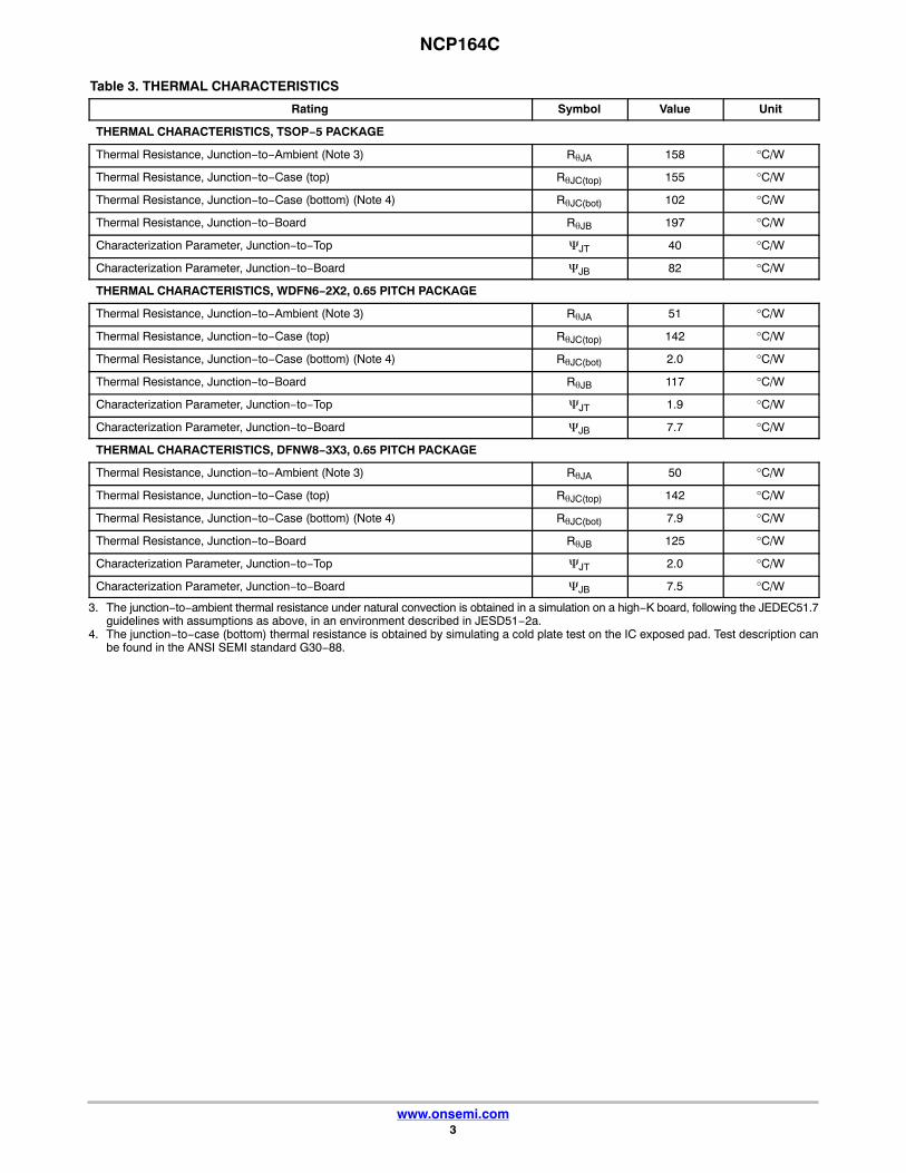
Table 3. THERMAL CHARACTERISTICS
Rating Symbol Value Unit
THERMAL CHARACTERISTICS, TSOP−5 PACKAGE
Thermal Resistance, Junction−to−Ambient (Note 3) R�JA 158 °C/W
Thermal Resistance, Junction−to−Case (top) R�JC(top) 155 °C/W
Thermal Resistance, Junction−to−Case (bottom) (Note 4) R�JC(bot) 102 °C/W
Thermal Resistance, Junction−to−Board R�JB 197 °C/W
Characterization Parameter, Junction−to−Top �JT 40 °C/W
Characterization Parameter, Junction−to−Board �JB 82 °C/W
THERMAL CHARACTERISTICS, WDFN6−2X2, 0.65 PITCH PACKAGE
Thermal Resistance, Junction−to−Ambient (Note 3) R�JA 51 °C/W
Thermal Resistance, Junction−to−Case (top) R�JC(top) 142 °C/W
Thermal Resistance, Junction−to−Case (bottom) (Note 4) R�JC(bot) 2.0 °C/W
Thermal Resistance, Junction−to−Board R�JB 117 °C/W
Characterization Parameter, Junction−to−Top �JT 1.9 °C/W
Characterization Parameter, Junction−to−Board �JB 7.7 °C/W
THERMAL CHARACTERISTICS, DFNW8−3X3, 0.65 PITCH PACKAGE
Thermal Resistance, Junction−to−Ambient (Note 3) R�JA 50 °C/W
Thermal Resistance, Junction−to−Case (top) R�JC(top) 142 °C/W
Thermal Resistance, Junction−to−Case (bottom) (Note 4) R�JC(bot) 7.9 °C/W
Thermal Resistance, Junction−to−Board R�JB 125 °C/W
Characterization Parameter, Junction−to−Top �JT 2.0 °C/W
Characterization Parameter, Junction−to−Board �JB 7.5 °C/W
3. The junction−to−ambient thermal resistance under natural convection is obtained in a simulation on a high−K board, following the JEDEC51.7guidelines with assumptions as above, in an environment described in JESD51−2a.
4. The junction−to−case (bottom) thermal resistance is obtained by simulating a cold plate test on the IC exposed pad. Test description canbe found in the ANSI SEMI standard G30−88.
NCP164C
www.onsemi.com4
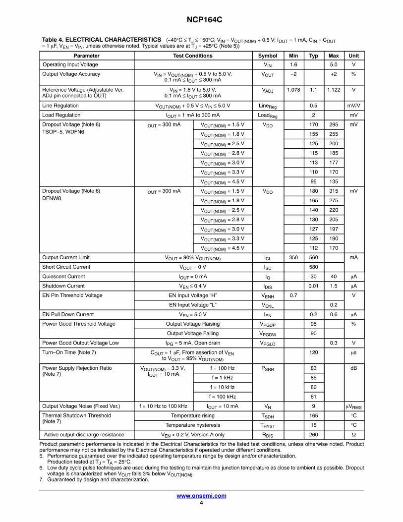
Table 4. ELECTRICAL CHARACTERISTICS (−40°C ≤ TJ ≤ 150°C; VIN = VOUT(NOM) + 0.5 V; IOUT = 1 mA, CIN = COUT= 1 �F, VEN = VIN, unless otherwise noted. Typical values are at TJ = +25°C (Note 5))
Parameter Test Conditions Symbol Min Typ Max Unit
Operating Input Voltage VIN 1.6 5.0 V
Output Voltage Accuracy VIN = VOUT(NOM) + 0.5 V to 5.0 V,0.1 mA ≤ IOUT ≤ 300 mA
VOUT −2 +2 %
Reference Voltage (Adjustable Ver. ADJ pin connected to OUT)
VIN = 1.6 V to 5.0 V,0.1 mA ≤ IOUT ≤ 300 mA
VADJ 1.078 1.1 1.122 V
Line Regulation VOUT(NOM) + 0.5 V ≤ VIN ≤ 5.0 V LineReg 0.5 mV/V
Load Regulation IOUT = 1 mA to 300 mA LoadReg 2 mV
Dropout Voltage (Note 6) TSOP−5, WDFN6
IOUT = 300 mA VOUT(NOM) = 1.5 V VDO 170 295 mV
VOUT(NOM) = 1.8 V 155 255
VOUT(NOM) = 2.5 V 125 200
VOUT(NOM) = 2.8 V 115 185
VOUT(NOM) = 3.0 V 113 177
VOUT(NOM) = 3.3 V 110 170
VOUT(NOM) = 4.5 V 95 135
Dropout Voltage (Note 6) DFNW8
IOUT = 300 mA VOUT(NOM) = 1.5 V VDO 180 315 mV
VOUT(NOM) = 1.8 V 165 275
VOUT(NOM) = 2.5 V 140 220
VOUT(NOM) = 2.8 V 130 205
VOUT(NOM) = 3.0 V 127 197
VOUT(NOM) = 3.3 V 125 190
VOUT(NOM) = 4.5 V 112 170
Output Current Limit VOUT = 90% VOUT(NOM) ICL 350 560 mA
Short Circuit Current VOUT = 0 V ISC 580
Quiescent Current IOUT = 0 mA IQ 30 40 �A
Shutdown Current VEN ≤ 0.4 V IDIS 0.01 1.5 �A
EN Pin Threshold Voltage EN Input Voltage “H” VENH 0.7 V
EN Input Voltage “L” VENL 0.2
EN Pull Down Current VEN = 5.0 V IEN 0.2 0.6 �A
Power Good Threshold Voltage Output Voltage Raising VPGUP 95 %
Output Voltage Falling VPGDW 90
Power Good Output Voltage Low IPG = 5 mA, Open drain VPGLO 0.3 V
Turn−On Time (Note 7) COUT = 1 �F, From assertion of VEN to VOUT = 95% VOUT(NOM)
120 �s
Power Supply Rejection Ratio (Note 7)
VOUT(NOM) = 3.3 V, IOUT = 10 mA
f = 100 Hz PSRR 83 dB
f = 1 kHz 85
f = 10 kHz 80
f = 100 kHz 61
Output Voltage Noise (Fixed Ver.) f = 10 Hz to 100 kHz IOUT = 10 mA VN 9 �VRMS
Thermal Shutdown Threshold (Note 7)
Temperature rising TSDH 165 °C
Temperature hysteresis THYST 15 °C
Active output discharge resistance VEN < 0.2 V, Version A only RDIS 260 �
Product parametric performance is indicated in the Electrical Characteristics for the listed test conditions, unless otherwise noted. Productperformance may not be indicated by the Electrical Characteristics if operated under different conditions.5. Performance guaranteed over the indicated operating temperature range by design and/or characterization.
Production tested at TJ = TA = 25°C.6. Low duty cycle pulse techniques are used during the testing to maintain the junction temperature as close to ambient as possible. Dropout
voltage is characterized when VOUT falls 3% below VOUT(NOM).7. Guaranteed by design and characterization.
NCP164C
www.onsemi.com5
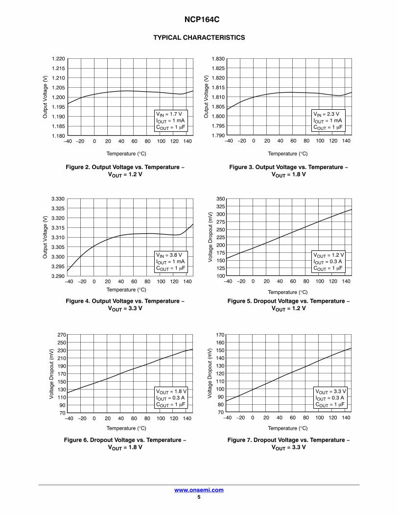
TYPICAL CHARACTERISTICS
Figure 2. Output Voltage vs. Temperature −VOUT = 1.2 V
Figure 3. Output Voltage vs. Temperature −VOUT = 1.8 V
Figure 4. Output Voltage vs. Temperature −VOUT = 3.3 V
Figure 5. Dropout Voltage vs. Temperature −VOUT = 1.2 V
Figure 6. Dropout Voltage vs. Temperature −VOUT = 1.8 V
Figure 7. Dropout Voltage vs. Temperature −VOUT = 3.3 V
1.180
1.185
1.190
1.195
1.200
1.205
1.210
1.215
1.220
−40 −20 0 20 40 60 80 100 120 140
Out
put V
olta
ge (
V)
Temperature (°C)
VIN = 1.7 VIOUT = 1 mACOUT = 1 �F
1.790
1.795
1.800
1.805
1.810
1.815
1.820
1.825
1.830
−40 −20 0 20 40 60 80 100 120 140
Out
put V
olta
ge (
V)
VIN = 2.3 VIOUT = 1 mACOUT = 1 �F
Temperature (°C)
3.290
3.295
3.300
3.305
3.310
3.315
3.320
3.325
3.330
−40 −20 0 20 40 60 80 100 120 140
Out
put V
olta
ge (
V)
100
125
150
175
200
225
250
275
300
325
350
−40 −20 0 20 40 60 80 100 120 140
Vol
tage
Dro
pout
(m
V)
VIN = 3.8 VIOUT = 1 mACOUT = 1 �F
VOUT = 1.2 VIOUT = 0.3 ACOUT = 1 �F
70
90
110
130
150
170
190
210
230
250
270
−40 −20 0 20 40 60 80 100 120 140
Vol
tage
Dro
pout
(m
V)
70
80
90
100
110
120
130
140
150
160
170
−40 −20 0 20 40 60 80 100 120 140
Vol
tage
Dro
pout
(m
V)
Temperature (°C) Temperature (°C)
Temperature (°C) Temperature (°C)
VOUT = 1.8 VIOUT = 0.3 ACOUT = 1 �F
VOUT = 3.3 VIOUT = 0.3 ACOUT = 1 �F
NCP164C
www.onsemi.com6
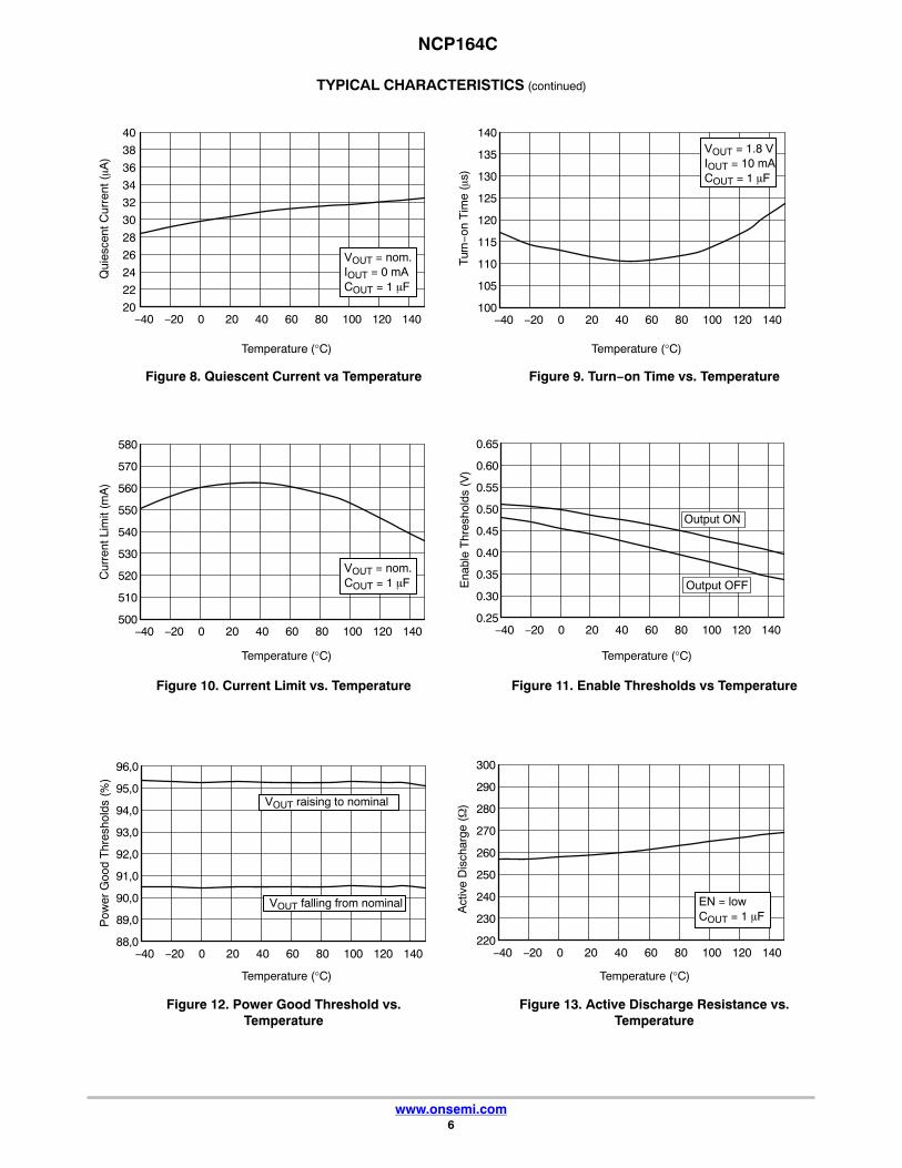
TYPICAL CHARACTERISTICS (continued)
Figure 8. Quiescent Current va Temperature Figure 9. Turn−on Time vs. Temperature
Figure 10. Current Limit vs. Temperature Figure 11. Enable Thresholds vs Temperature
Figure 12. Power Good Threshold vs.Temperature
Figure 13. Active Discharge Resistance vs.Temperature
Temperature (°C)
20
22
24
26
28
30
32
34
36
38
40
−40 −20 0 20 40 60 80 100 120 140
Qui
esce
nt C
urre
nt (�A
)
100
105
110
115
120
125
130
135
140
−40 −20 0 20 40 60 80 100 120 140
Turn−
on T
ime
(�s)
VOUT = nom.IOUT = 0 mACOUT = 1 �F
VOUT = 1.8 VIOUT = 10 mACOUT = 1 �F
Temperature (°C)
500
510
520
530
540
550
560
570
580
−40 −20 0 20 40 60 80 100 120 140
Cur
rent
Lim
it (m
A)
0.25
0.30
0.35
0.40
0.45
0.50
0.55
0.60
0.65
−40 −20 0 20 40 60 80 100 120 140
Ena
ble
Thr
esho
lds
(V)
VOUT = nom.COUT = 1 �F
Output ON
Output OFF
88,0
89,0
90,0
91,0
92,0
93,0
94,0
95,0
96,0
−40 −20 0 20 40 60 80 100 120 140
Pow
er G
ood
Thr
esho
lds
(%)
220
230
240
250
260
270
280
290
300
−40 −20 0 20 40 60 80 100 120 140
Act
ive
Dis
char
ge (�
)VOUT raising to nominal
VOUT falling from nominal
Temperature (°C)
EN = lowCOUT = 1 �F
Temperature (°C)
Temperature (°C) Temperature (°C)
NCP164C
www.onsemi.com7
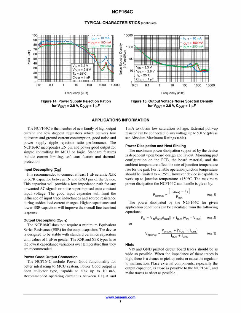
TYPICAL CHARACTERISTICS (continued)
Figure 14. Power Supply Rejection Rationfor VOUT = 2.8 V, COUT = 1 �F
Figure 15. Output Voltage Noise Spectral Densityfor VOUT = 2.8 V, COUT = 1 �F
Frequency (kHz)
0
10
20
30
40
50
60
70
80
90
100
0.01 0,1 1 10 100 1000 10000
PS
RR
(dB
)
1
10
100
1000
10000
0.01 0.1 1 10 100 1000 10000
Noi
se S
pect
ral D
ensi
ty(n
V/s
qrt(
Hz)
)
Frequency (kHz)
- IOUT = 10 mA- IOUT = 100 mA- IOUT = 200 mA
VIN = 3.2 VVOUT = 2.8 VTA = 25°CCOUT = 1 �F
- IOUT = 10 mA- IOUT = 100 mA- IOUT = 200 mA
VIN = 3.3 VVOUT = 2.8 VTA = 25°CCOUT = 1 �F
APPLICATIONS INFORMATION
The NCP164C is the member of new family of high outputcurrent and low dropout regulators which delivers lowquiescent and ground current consumption, good noise andpower supply ripple rejection ratio performance. TheNCP164C incorporates EN pin and power good output forsimple controlling by MCU or logic. Standard featuresinclude current limiting, soft−start feature and thermalprotection.
Input Decoupling (CIN)It is recommended to connect at least 1 �F ceramic X5R
or X7R capacitor between IN and GND pin of the device.This capacitor will provide a low impedance path for anyunwanted AC signals or noise superimposed onto constantinput voltage. The good input capacitor will limit theinfluence of input trace inductances and source resistanceduring sudden load current changes. Higher capacitance andlower ESR capacitors will improve the overall line transientresponse.
Output Decoupling (COUT)The NCP164C does not require a minimum Equivalent
Series Resistance (ESR) for the output capacitor. The deviceis designed to be stable with standard ceramics capacitorswith values of 1 �F or greater. The X5R and X7R types havethe lowest capacitance variations over temperature thus theyare recommended.
Power Good Output ConnectionThe NCP164C include Power Good functionality for
better interfacing to MCU system. Power Good output isopen collector type, capable to sink up to 10 mA.Recommended operating current is between 10 �A and
1 mA to obtain low saturation voltage. External pull−upresistor can be connected to any voltage up to 5.0 V (pleasesee Absolute Maximum Ratings table).
Power Dissipation and Heat SinkingThe maximum power dissipation supported by the device
is dependent upon board design and layout. Mounting padconfiguration on the PCB, the board material, and theambient temperature affect the rate of junction temperaturerise for the part. For reliable operation junction temperatureshould be limited to +125°C, however device is capable towork up to junction temperature +150°C. The maximumpower dissipation the NCP164C can handle is given by:
PD(MAX) ��TJ(MAX) � TA
�R�JA
(eq. 1)
The power dissipated by the NCP164C for givenapplication conditions can be calculated from the followingequations:
PD � VIN(IGND(IOUT)) � IOUT (VIN � VOUT) (eq. 2)
or
VIN(MAX) �PD(MAX) � �VOUT IOUT
IOUT � IGND
(eq. 3)
HintsVIN and GND printed circuit board traces should be as
wide as possible. When the impedance of these traces ishigh, there is a chance to pick up noise or cause the regulatorto malfunction. Place external components, especially theoutput capacitor, as close as possible to the NCP164C, andmake traces as short as possible.
NCP164C
www.onsemi.com8
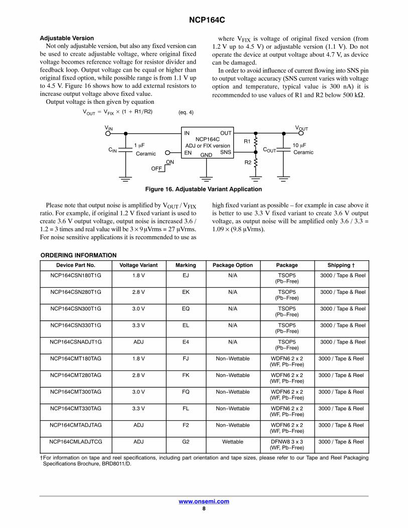
Adjustable VersionNot only adjustable version, but also any fixed version can
be used to create adjustable voltage, where original fixedvoltage becomes reference voltage for resistor divider andfeedback loop. Output voltage can be equal or higher thanoriginal fixed option, while possible range is from 1.1 V upto 4.5 V. Figure 16 shows how to add external resistors toincrease output voltage above fixed value.
Output voltage is then given by equation
VOUT � VFIX (1 � R1�R2) (eq. 4)
where VFIX is voltage of original fixed version (from1.2 V up to 4.5 V) or adjustable version (1.1 V). Do notoperate the device at output voltage about 4.7 V, as devicecan be damaged.
In order to avoid influence of current flowing into SNS pinto output voltage accuracy (SNS current varies with voltageoption and temperature, typical value is 300 nA) it isrecommended to use values of R1 and R2 below 500 k�.
Figure 16. Adjustable Variant Application
R1
Ceramic
NCP164CADJ or FIX version
IN OUT
GNDCeramic EN
OFFON R2
SNS1 �F
VIN
CIN
VOUT
10 �FCOUT
Please note that output noise is amplified by VOUT / VFIXratio. For example, if original 1.2 V fixed variant is used tocreate 3.6 V output voltage, output noise is increased 3.6 /1.2 = 3 times and real value will be 3 × 9 �Vrms = 27��Vrms.For noise sensitive applications it is recommended to use as
high fixed variant as possible – for example in case above itis better to use 3.3 V fixed variant to create 3.6 V outputvoltage, as output noise will be amplified only 3.6 / 3.3 =1.09 × (9.8 �Vrms).
ORDERING INFORMATION
Device Part No. Voltage Variant Marking Package Option Package Shipping †
NCP164CSN180T1G 1.8 V EJ N/A TSOP5(Pb−Free)
3000 / Tape & Reel
NCP164CSN280T1G 2.8 V EK N/A TSOP5(Pb−Free)
3000 / Tape & Reel
NCP164CSN300T1G 3.0 V EQ N/A TSOP5(Pb−Free)
3000 / Tape & Reel
NCP164CSN330T1G 3.3 V EL N/A TSOP5(Pb−Free)
3000 / Tape & Reel
NCP164CSNADJT1G ADJ E4 N/A TSOP5(Pb−Free)
3000 / Tape & Reel
NCP164CMT180TAG 1.8 V FJ Non−Wettable WDFN6 2 x 2(WF, Pb−Free)
3000 / Tape & Reel
NCP164CMT280TAG 2.8 V FK Non−Wettable WDFN6 2 x 2(WF, Pb−Free)
3000 / Tape & Reel
NCP164CMT300TAG 3.0 V FQ Non−Wettable WDFN6 2 x 2(WF, Pb−Free)
3000 / Tape & Reel
NCP164CMT330TAG 3.3 V FL Non−Wettable WDFN6 2 x 2(WF, Pb−Free)
3000 / Tape & Reel
NCP164CMTADJTAG ADJ F2 Non−Wettable WDFN6 2 x 2(WF, Pb−Free)
3000 / Tape & Reel
NCP164CMLADJTCG ADJ G2 Wettable DFNW8 3 x 3(WF, Pb−Free)
3000 / Tape & Reel
†For information on tape and reel specifications, including part orientation and tape sizes, please refer to our Tape and Reel PackagingSpecifications Brochure, BRD8011/D.
NCP164C
www.onsemi.com9
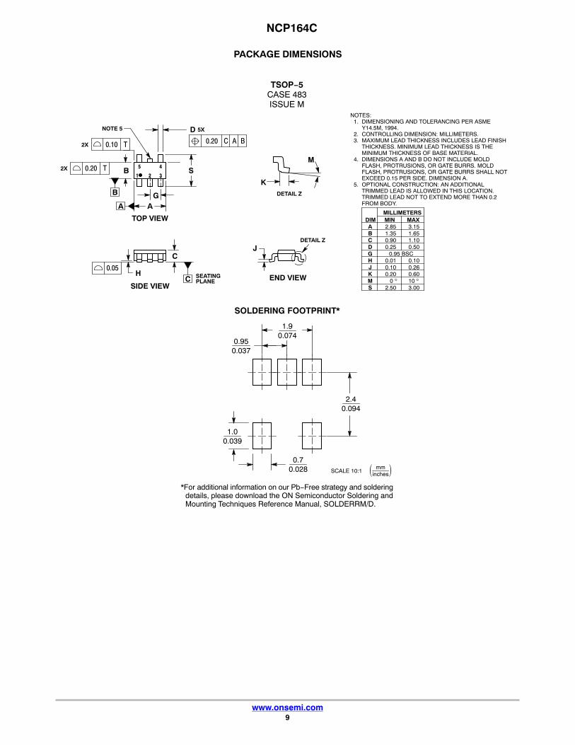
PACKAGE DIMENSIONS
TSOP−5CASE 483ISSUE M
0.70.028
1.00.039
� mminches
SCALE 10:1
0.950.037
2.40.094
1.90.074
*For additional information on our Pb−Free strategy and solderingdetails, please download the ON Semiconductor Soldering andMounting Techniques Reference Manual, SOLDERRM/D.
SOLDERING FOOTPRINT*
NOTES:1. DIMENSIONING AND TOLERANCING PER ASME
Y14.5M, 1994.2. CONTROLLING DIMENSION: MILLIMETERS.3. MAXIMUM LEAD THICKNESS INCLUDES LEAD FINISH
THICKNESS. MINIMUM LEAD THICKNESS IS THEMINIMUM THICKNESS OF BASE MATERIAL.
4. DIMENSIONS A AND B DO NOT INCLUDE MOLDFLASH, PROTRUSIONS, OR GATE BURRS. MOLDFLASH, PROTRUSIONS, OR GATE BURRS SHALL NOTEXCEED 0.15 PER SIDE. DIMENSION A.
5. OPTIONAL CONSTRUCTION: AN ADDITIONALTRIMMED LEAD IS ALLOWED IN THIS LOCATION.TRIMMED LEAD NOT TO EXTEND MORE THAN 0.2FROM BODY.
DIM MIN MAXMILLIMETERS
ABC 0.90 1.10D 0.25 0.50G 0.95 BSCH 0.01 0.10J 0.10 0.26K 0.20 0.60M 0 10 S 2.50 3.00
1 2 3
5 4S
AG
B
D
H
CJ
� �
0.20
5X
C A BT0.102X
2X T0.20
NOTE 5
C SEATINGPLANE
0.05
K
M
DETAIL Z
DETAIL Z
TOP VIEW
SIDE VIEW
A
B
END VIEW
1.35 1.652.85 3.15
NCP164C
www.onsemi.com10
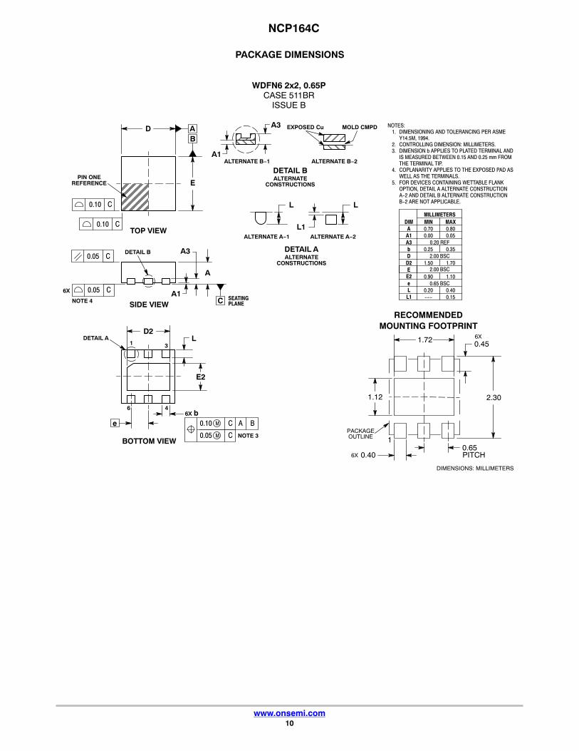
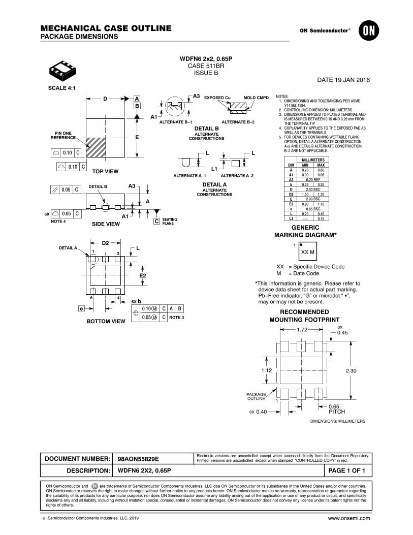
PACKAGE DIMENSIONS
WDFN6 2x2, 0.65PCASE 511BR
ISSUE B
ÍÍÍÍÍÍÍÍÍ
NOTES:1. DIMENSIONING AND TOLERANCING PER ASME
Y14.5M, 1994.2. CONTROLLING DIMENSION: MILLIMETERS.3. DIMENSION b APPLIES TO PLATED TERMINAL AND
IS MEASURED BETWEEN 0.15 AND 0.25 mm FROMTHE TERMINAL TIP.
4. COPLANARITY APPLIES TO THE EXPOSED PAD ASWELL AS THE TERMINALS.
5. FOR DEVICES CONTAINING WETTABLE FLANKOPTION, DETAIL A ALTERNATE CONSTRUCTIONA-2 AND DETAIL B ALTERNATE CONSTRUCTIONB-2 ARE NOT APPLICABLE.
SEATINGPLANE
D
E
0.10 C
A3
A
A1
0.10 C DIMA
MIN MAXMILLIMETERS
0.70 0.80A1 0.00 0.05A3 0.20 REFb 0.25 0.35D 2.00 BSCD2 1.50 1.70
0.90 1.10E 2.00 BSCE2e 0.65 BSC
0.20 0.40L
PIN ONEREFERENCE
0.05 C
0.05 C
NOTE 4
A0.10 C
NOTE 3
L
e
D2
E2
bB
3
66X
1
4
0.05 C
MOUNTING FOOTPRINT
BOTTOM VIEW
RECOMMENDED
DIMENSIONS: MILLIMETERS
L1
DETAIL A
L
ALTERNATECONSTRUCTIONS
L
DETAIL A
DETAIL B
AB
TOP VIEW
CSIDE VIEW--- 0.15L1
6X0.45
2.301.12
1.72
0.65PITCH6X 0.40
1PACKAGEOUTLINE
6X
M
M
ÉÉÇÇÇÇ
DETAIL B
MOLD CMPDEXPOSED Cu
ALTERNATECONSTRUCTIONS
ÉÉÇÇA1
A3
ALTERNATE B−2ALTERNATE B−1
ALTERNATE A−2ALTERNATE A−1
NCP164C
www.onsemi.com11
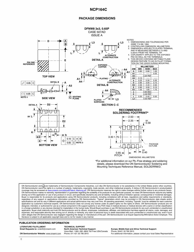
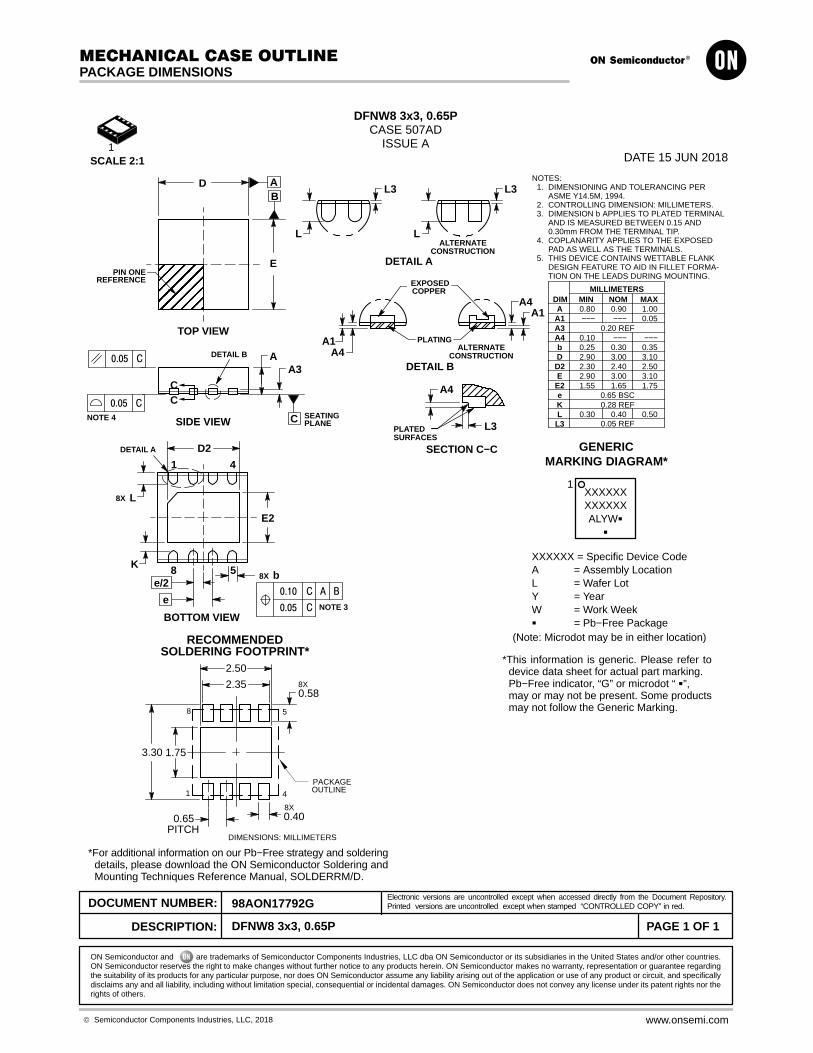
PACKAGE DIMENSIONS
DFNW8 3x3, 0.65PCASE 507AD
ISSUE A
NOTES:1. DIMENSIONING AND TOLERANCING PER
ASME Y14.5M, 1994.2. CONTROLLING DIMENSION: MILLIMETERS.3. DIMENSION b APPLIES TO PLATED TERMINAL
AND IS MEASURED BETWEEN 0.15 AND0.30mm FROM THE TERMINAL TIP.
4. COPLANARITY APPLIES TO THE EXPOSEDPAD AS WELL AS THE TERMINALS.
5. THIS DEVICE CONTAINS WETTABLE FLANKDESIGN FEATURE TO AID IN FILLET FORMA-TION ON THE LEADS DURING MOUNTING.ÉÉÉ
ÉÉÉÉÉÉ
AB
E
D
D2
E2
BOTTOM VIEW
b
e
8X
0.10 B
0.05
AC
C NOTE 3
PIN ONEREFERENCE
TOP VIEW
AA3
0.05 C
0.05 C
C SEATINGPLANESIDE VIEW
L8X
1 4
58
*For additional information on our Pb−Free strategy and solderingdetails, please download the ON Semiconductor Soldering andMounting Techniques Reference Manual, SOLDERRM/D.
RECOMMENDED
DETAIL B
DETAIL A
NOTE 4
e/2
SOLDERING FOOTPRINT*
DIM MIN NOMMILLIMETERS
A 0.80 0.90A1 −−− −−−
b 0.25 0.30DD2 2.30 2.40E
E2 1.55 1.65e 0.65 BSC
L 0.30 0.40
A3 0.20 REF
2.90 3.00
K
A4
L3
MAX
2.90 3.00
1.000.05
0.35
2.50
1.75
0.50
3.10
3.10
ALTERNATECONSTRUCTION
DETAIL A
L3
SECTION C−C
PLATED
A4
SURFACESL3
L3
L
DETAIL B
PLATING
EXPOSED
ALTERNATECONSTRUCTION
COPPER
A4A1
A4A1
L
CC
PACKAGEOUTLINE1 4
8 5
8X0.58
2.50
1.75
0.400.65PITCH
3.30
8X
DIMENSIONS: MILLIMETERS
2.35
K
0.28 REF
0.05 REF
0.10 −−− −−−
ON Semiconductor and are trademarks of Semiconductor Components Industries, LLC dba ON Semiconductor or its subsidiaries in the United States and/or other countries.ON Semiconductor owns the rights to a number of patents, trademarks, copyrights, trade secrets, and other intellectual property. A listing of ON Semiconductor’s product/patentcoverage may be accessed at www.onsemi.com/site/pdf/Patent−Marking.pdf. ON Semiconductor reserves the right to make changes without further notice to any products herein.ON Semiconductor makes no warranty, representation or guarantee regarding the suitability of its products for any particular purpose, nor does ON Semiconductor assume any liabilityarising out of the application or use of any product or circuit, and specifically disclaims any and all liability, including without limitation special, consequential or incidental damages.Buyer is responsible for its products and applications using ON Semiconductor products, including compliance with all laws, regulations and safety requirements or standards,regardless of any support or applications information provided by ON Semiconductor. “Typical” parameters which may be provided in ON Semiconductor data sheets and/orspecifications can and do vary in different applications and actual performance may vary over time. All operating parameters, including “Typicals” must be validated for each customerapplication by customer’s technical experts. ON Semiconductor does not convey any license under its patent rights nor the rights of others. ON Semiconductor products are notdesigned, intended, or authorized for use as a critical component in life support systems or any FDA Class 3 medical devices or medical devices with a same or similar classificationin a foreign jurisdiction or any devices intended for implantation in the human body. Should Buyer purchase or use ON Semiconductor products for any such unintended or unauthorizedapplication, Buyer shall indemnify and hold ON Semiconductor and its officers, employees, subsidiaries, affiliates, and distributors harmless against all claims, costs, damages, andexpenses, and reasonable attorney fees arising out of, directly or indirectly, any claim of personal injury or death associated with such unintended or unauthorized use, even if suchclaim alleges that ON Semiconductor was negligent regarding the design or manufacture of the part. ON Semiconductor is an Equal Opportunity/Affirmative Action Employer. Thisliterature is subject to all applicable copyright laws and is not for resale in any manner.
PUBLICATION ORDERING INFORMATIONTECHNICAL SUPPORTNorth American Technical Support:Voice Mail: 1 800−282−9855 Toll Free USA/CanadaPhone: 011 421 33 790 2910
LITERATURE FULFILLMENT:Email Requests to: [email protected]
ON Semiconductor Website: www.onsemi.com
Europe, Middle East and Africa Technical Support:Phone: 00421 33 790 2910For additional information, please contact your local Sales Representative
◊
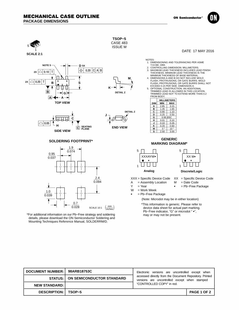
TSOP−5
CASE 483ISSUE M
DATE 17 MAY 2016SCALE 2:1
1
5
XX M�
�
GENERICMARKING DIAGRAM*
15
0.70.028
1.00.039
� mminches
�SCALE 10:1
0.950.037
2.40.094
1.90.074
*For additional information on our Pb−Free strategy and solderingdetails, please download the ON Semiconductor Soldering andMounting Techniques Reference Manual, SOLDERRM/D.
SOLDERING FOOTPRINT*
*This information is generic. Please refer todevice data sheet for actual part marking.Pb−Free indicator, “G” or microdot “ �”,may or may not be present.
XXX = Specific Device CodeA = Assembly LocationY = YearW = Work Week� = Pb−Free Package
1
5
XXXAYW�
�
Discrete/LogicAnalog
(Note: Microdot may be in either location)
XX = Specific Device CodeM = Date Code� = Pb−Free Package
NOTES:1. DIMENSIONING AND TOLERANCING PER ASME
Y14.5M, 1994.2. CONTROLLING DIMENSION: MILLIMETERS.3. MAXIMUM LEAD THICKNESS INCLUDES LEAD FINISH
THICKNESS. MINIMUM LEAD THICKNESS IS THEMINIMUM THICKNESS OF BASE MATERIAL.
4. DIMENSIONS A AND B DO NOT INCLUDE MOLDFLASH, PROTRUSIONS, OR GATE BURRS. MOLDFLASH, PROTRUSIONS, OR GATE BURRS SHALL NOTEXCEED 0.15 PER SIDE. DIMENSION A.
5. OPTIONAL CONSTRUCTION: AN ADDITIONALTRIMMED LEAD IS ALLOWED IN THIS LOCATION.TRIMMED LEAD NOT TO EXTEND MORE THAN 0.2FROM BODY.
DIM MIN MAXMILLIMETERS
ABC 0.90 1.10D 0.25 0.50G 0.95 BSCH 0.01 0.10J 0.10 0.26K 0.20 0.60M 0 10 S 2.50 3.00
1 2 3
5 4S
AG
B
D
H
CJ
� �
0.20
5X
C A BT0.102X
2X T0.20
NOTE 5
C SEATINGPLANE
0.05
K
M
DETAIL Z
DETAIL Z
TOP VIEW
SIDE VIEW
A
B
END VIEW
1.35 1.652.85 3.15
MECHANICAL CASE OUTLINE
PACKAGE DIMENSIONS
http://onsemi.com1
© Semiconductor Components Industries, LLC, 2002
October, 2002 − Rev. 0Case Outline Number:
XXX
DOCUMENT NUMBER:
STATUS:
NEW STANDARD:
DESCRIPTION:
98ARB18753C
ON SEMICONDUCTOR STANDARD
TSOP−5
Electronic versions are uncontrolled except when accessed directly from the Document Repository. Printed versions are uncontrolled except when stamped “CONTROLLED COPY” in red.
PAGE 1 OF 2

DOCUMENT NUMBER:98ARB18753C
PAGE 2 OF 2
ISSUE REVISION DATE
O INITIATED NEW MECHANICAL OUTLINE #483. REQ BY WL CHIN/L. RENNICK. 28 OCT 1998
A UPDATE OUTLINE DRAWING TO CORRECT DIN “C” (SHOULD BE FROM TIP OFLID TO TOP OF PKG). DIM IN TABLE INCORRECTLY LISTED TO G, F TO H,H TO J, N TO L & R TO M. REQ BY F. PADILLA
13 NOV 1998
B CHANGE OF LEGAL ONWERSHIP FROM MOTOROLA TO ON SEMICONDUC-TOR. REQ BY A. GARLINGTON
20 APR 2001
C ADDED NOTE “4”. REQ BY S. RIGGS 27 JUN 2003
D ADDED FOOTPRINT INFORMATION. UPDATED MARKING. REQ. BY D. JOERSZ 07 APR 2005
E CHANGED DEVICE MARKING FROM AWW TO AYW. REQ. BY J. MANES. 14 SEP 2005
F UPDATED DRAWINGS TO LATEST JEDEC STANDARDS. ADDED NOTE 5. REQ.BY T. GURNETT.
07 JUN 2006
G ADDED MARKING DIAGRAM FOR IC OPTION. REQ. BY J. MILLER. 21 FEB 2007
H CORRECTED MARKING DIAGRAM ERROR BY REVERSING ANALOG ANDDISCRETE LABELS. REQ. BY GK SUA.
18 MAY 2007
J CHANGED NOTE 4. REQ. BY A. GARLINGTON. 13 MAR 2013
K REMOVED DIMENSION L AND ADDED DATUMS A AND B TO TOP VIEW. REQ.BY A. GARLINGTON.
19 APR 2013
L REMOVED −02 FROM CASE CODE VARIANT. REQ. BY N. CALZADA. 23 SEP 2015
M CHANGED DIMENSIONS A & B FROM BASIC TO MIN AND MAX VALUES. REQ.BY A. GARLINGTON.
17 MAY 2016
© Semiconductor Components Industries, LLC, 2016
May, 2016 − Rev. MCase Outline Number:
483
ON Semiconductor and are registered trademarks of Semiconductor Components Industries, LLC (SCILLC). SCILLC reserves the right to make changes without further noticeto any products herein. SCILLC makes no warranty, representation or guarantee regarding the suitability of its products for any particular purpose, nor does SCILLC assume any liabilityarising out of the application or use of any product or circuit, and specifically disclaims any and all liability, including without limitation special, consequential or incidental damages.“Typical” parameters which may be provided in SCILLC data sheets and/or specifications can and do vary in different applications and actual performance may vary over time. Alloperating parameters, including “Typicals” must be validated for each customer application by customer’s technical experts. SCILLC does not convey any license under its patent rightsnor the rights of others. SCILLC products are not designed, intended, or authorized for use as components in systems intended for surgical implant into the body, or other applicationsintended to support or sustain life, or for any other application in which the failure of the SCILLC product could create a situation where personal injury or death may occur. ShouldBuyer purchase or use SCILLC products for any such unintended or unauthorized application, Buyer shall indemnify and hold SCILLC and its officers, employees, subsidiaries, affiliates,and distributors harmless against all claims, costs, damages, and expenses, and reasonable attorney fees arising out of, directly or indirectly, any claim of personal injury or deathassociated with such unintended or unauthorized use, even if such claim alleges that SCILLC was negligent regarding the design or manufacture of the part. SCILLC is an EqualOpportunity/Affirmative Action Employer. This literature is subject to all applicable copyright laws and is not for resale in any manner.
DFNW8 3x3, 0.65PCASE 507AD
ISSUE ADATE 15 JUN 2018SCALE 2:1
NOTES:1. DIMENSIONING AND TOLERANCING PER
ASME Y14.5M, 1994.2. CONTROLLING DIMENSION: MILLIMETERS.3. DIMENSION b APPLIES TO PLATED TERMINAL
AND IS MEASURED BETWEEN 0.15 AND0.30mm FROM THE TERMINAL TIP.
4. COPLANARITY APPLIES TO THE EXPOSEDPAD AS WELL AS THE TERMINALS.
5. THIS DEVICE CONTAINS WETTABLE FLANKDESIGN FEATURE TO AID IN FILLET FORMA-TION ON THE LEADS DURING MOUNTING.
ÉÉÉÉÉÉÉÉÉÉÉÉ
AB
E
D
D2
E2
BOTTOM VIEW
b
e
8X
0.10 B
0.05
AC
C NOTE 3
PIN ONEREFERENCE
TOP VIEW
AA3
0.05 C
0.05 C
C SEATINGPLANESIDE VIEW
L8X
1 4
58
1
*For additional information on our Pb−Free strategy and solderingdetails, please download the ON Semiconductor Soldering andMounting Techniques Reference Manual, SOLDERRM/D.
RECOMMENDED
DETAIL B
DETAIL A
NOTE 4
e/2
GENERICMARKING DIAGRAM*
XXXXXX = Specific Device CodeA = Assembly LocationL = Wafer LotY = YearW = Work Week� = Pb−Free Package
XXXXXXXXXXXXALYW�
�
1
(Note: Microdot may be in either location)SOLDERING FOOTPRINT*
DIM MIN NOMMILLIMETERS
A 0.80 0.90A1 −−− −−−
b 0.25 0.30DD2 2.30 2.40E
E2 1.55 1.65e 0.65 BSC
L 0.30 0.40
A3 0.20 REF
2.90 3.00
K
A4
L3
MAX
2.90 3.00
1.000.05
0.35
2.50
1.75
0.50
3.10
3.10
ALTERNATECONSTRUCTION
DETAIL A
L3
SECTION C−C
PLATED
A4
SURFACESL3
L3
L
DETAIL B
PLATING
EXPOSED
ALTERNATECONSTRUCTION
COPPER
A4A1
A4A1
L
CC
PACKAGEOUTLINE1 4
8 5
8X0.58
2.50
1.75
0.400.65PITCH
3.30
8X
DIMENSIONS: MILLIMETERS
2.35
K
0.28 REF
0.05 REF
*This information is generic. Please refer todevice data sheet for actual part marking.Pb−Free indicator, “G” or microdot “ �”,may or may not be present. Some productsmay not follow the Generic Marking.
0.10 −−− −−−
MECHANICAL CASE OUTLINE
PACKAGE DIMENSIONS
ON Semiconductor and are trademarks of Semiconductor Components Industries, LLC dba ON Semiconductor or its subsidiaries in the United States and/or other countries.ON Semiconductor reserves the right to make changes without further notice to any products herein. ON Semiconductor makes no warranty, representation or guarantee regardingthe suitability of its products for any particular purpose, nor does ON Semiconductor assume any liability arising out of the application or use of any product or circuit, and specificallydisclaims any and all liability, including without limitation special, consequential or incidental damages. ON Semiconductor does not convey any license under its patent rights nor therights of others.
98AON17792GDOCUMENT NUMBER:
DESCRIPTION:
Electronic versions are uncontrolled except when accessed directly from the Document Repository.Printed versions are uncontrolled except when stamped “CONTROLLED COPY” in red.
PAGE 1 OF 1DFNW8 3x3, 0.65P
© Semiconductor Components Industries, LLC, 2018 www.onsemi.com
ÍÍÍÍÍÍÍÍÍ
NOTES:1. DIMENSIONING AND TOLERANCING PER ASME
Y14.5M, 1994.2. CONTROLLING DIMENSION: MILLIMETERS.3. DIMENSION b APPLIES TO PLATED TERMINAL AND
IS MEASURED BETWEEN 0.15 AND 0.25 mm FROMTHE TERMINAL TIP.
4. COPLANARITY APPLIES TO THE EXPOSED PAD ASWELL AS THE TERMINALS.
5. FOR DEVICES CONTAINING WETTABLE FLANKOPTION, DETAIL A ALTERNATE CONSTRUCTIONA-2 AND DETAIL B ALTERNATE CONSTRUCTIONB-2 ARE NOT APPLICABLE.
SEATINGPLANE
D
E
0.10 C
A3
A
A1
0.10 C
WDFN6 2x2, 0.65PCASE 511BR
ISSUE BDATE 19 JAN 2016
SCALE 4:1
DIMA
MIN MAXMILLIMETERS
0.70 0.80A1 0.00 0.05A3 0.20 REFb 0.25 0.35D 2.00 BSCD2 1.50 1.70
0.90 1.10E 2.00 BSCE2e 0.65 BSC
0.20 0.40L
PIN ONEREFERENCE
0.05 C
0.05 C
NOTE 4
A0.10 C
NOTE 3
L
e
D2
E2
bB
3
66X
1
4
0.05 C MOUNTING FOOTPRINT
GENERICMARKING DIAGRAM*
*This information is generic. Please refer todevice data sheet for actual part marking.Pb−Free indicator, “G” or microdot “ �”,may or may not be present.
XX = Specific Device CodeM = Date Code
XX M1
BOTTOM VIEW
RECOMMENDED
DIMENSIONS: MILLIMETERS
L1
DETAIL A
L
ALTERNATECONSTRUCTIONS
L
DETAIL A
DETAIL B
AB
TOP VIEW
CSIDE VIEW--- 0.15L1
6X0.45
2.301.12
1.72
0.65PITCH6X 0.40
1PACKAGEOUTLINE
6X
M
M
ÉÉÉÉÇÇ
DETAIL B
MOLD CMPDEXPOSED Cu
ALTERNATECONSTRUCTIONS
ÉÉÉÉÇÇ
A1
A3
ALTERNATE B−2ALTERNATE B−1
ALTERNATE A−2ALTERNATE A−1
MECHANICAL CASE OUTLINE
PACKAGE DIMENSIONS
ON Semiconductor and are trademarks of Semiconductor Components Industries, LLC dba ON Semiconductor or its subsidiaries in the United States and/or other countries.ON Semiconductor reserves the right to make changes without further notice to any products herein. ON Semiconductor makes no warranty, representation or guarantee regardingthe suitability of its products for any particular purpose, nor does ON Semiconductor assume any liability arising out of the application or use of any product or circuit, and specificallydisclaims any and all liability, including without limitation special, consequential or incidental damages. ON Semiconductor does not convey any license under its patent rights nor therights of others.
98AON55829EDOCUMENT NUMBER:
DESCRIPTION:
Electronic versions are uncontrolled except when accessed directly from the Document Repository.Printed versions are uncontrolled except when stamped “CONTROLLED COPY” in red.
PAGE 1 OF 1WDFN6 2X2, 0.65P
© Semiconductor Components Industries, LLC, 2019 www.onsemi.com
www.onsemi.com1
ON Semiconductor and are trademarks of Semiconductor Components Industries, LLC dba ON Semiconductor or its subsidiaries in the United States and/or other countries.ON Semiconductor owns the rights to a number of patents, trademarks, copyrights, trade secrets, and other intellectual property. A listing of ON Semiconductor’s product/patentcoverage may be accessed at www.onsemi.com/site/pdf/Patent−Marking.pdf. ON Semiconductor reserves the right to make changes without further notice to any products herein.ON Semiconductor makes no warranty, representation or guarantee regarding the suitability of its products for any particular purpose, nor does ON Semiconductor assume any liabilityarising out of the application or use of any product or circuit, and specifically disclaims any and all liability, including without limitation special, consequential or incidental damages.Buyer is responsible for its products and applications using ON Semiconductor products, including compliance with all laws, regulations and safety requirements or standards,regardless of any support or applications information provided by ON Semiconductor. “Typical” parameters which may be provided in ON Semiconductor data sheets and/orspecifications can and do vary in different applications and actual performance may vary over time. All operating parameters, including “Typicals” must be validated for each customerapplication by customer’s technical experts. ON Semiconductor does not convey any license under its patent rights nor the rights of others. ON Semiconductor products are notdesigned, intended, or authorized for use as a critical component in life support systems or any FDA Class 3 medical devices or medical devices with a same or similar classificationin a foreign jurisdiction or any devices intended for implantation in the human body. Should Buyer purchase or use ON Semiconductor products for any such unintended or unauthorizedapplication, Buyer shall indemnify and hold ON Semiconductor and its officers, employees, subsidiaries, affiliates, and distributors harmless against all claims, costs, damages, andexpenses, and reasonable attorney fees arising out of, directly or indirectly, any claim of personal injury or death associated with such unintended or unauthorized use, even if suchclaim alleges that ON Semiconductor was negligent regarding the design or manufacture of the part. ON Semiconductor is an Equal Opportunity/Affirmative Action Employer. Thisliterature is subject to all applicable copyright laws and is not for resale in any manner.
PUBLICATION ORDERING INFORMATIONTECHNICAL SUPPORTNorth American Technical Support:Voice Mail: 1 800−282−9855 Toll Free USA/CanadaPhone: 011 421 33 790 2910
LITERATURE FULFILLMENT:Email Requests to: [email protected]
ON Semiconductor Website: www.onsemi.com
Europe, Middle East and Africa Technical Support:Phone: 00421 33 790 2910For additional information, please contact your local Sales Representative
◊


![HIPDN: A POWER DISTRIBUTION NETWORK FOR ...transient response with a high level of efficiency [19, 15]. In this work, inductive switching regulator and low-dropout (LDO) regulator](https://static.fdocuments.net/doc/165x107/5fd731671b4f6640da3d62ab/hipdn-a-power-distribution-network-for-transient-response-with-a-high-level.jpg)