NCAB Group | Seminar no. 2 How to manufacture a PCB€¦ · What is a multilayer PCB? INTRODUCTION...
56
NCAB GROUP © | How to manufacture a PCB NCAB Group | Seminar no. 2 How to manufacture a PCB
-
Upload
vuongthuan -
Category
Documents
-
view
218 -
download
1
Transcript of NCAB Group | Seminar no. 2 How to manufacture a PCB€¦ · What is a multilayer PCB? INTRODUCTION...

NCAB GROUP © | How to manufacture a PCB
NCAB Group | Seminar no. 2
How to manufacture a PCB

2
Introduction to Multilayer PCBs

What is a multilayer PCB? INTRODUCTION TO MULTILAYER PCB´S
•! The green thing with holes in it.
•! The first item needed when building any piece of electronics, but often gets ordered last.
•! A platform for components.
•! Circuitry with pre-defined electrical function.
Three of more conductive layers of copper which have been bonded to non-conductive substrates, yet are electrically connected where needed, so that they can electrically connect specific electronic components using tracks, pads and other features (imaged and etched to form a bespoke design) in order to fulfill a specific function.
NCAB GROUP © | How to manufacture a PCB 3

History of PCBs INTRODUCTION TO MULTILAYER PCB´S
1903 First PCB-patent 1903-1946 Single / double sided boards (NPTH) 1947! Double sided, plated through holes developed
1960! Multilayer process developed.
1993! NCAB was founded (1986 in Malaysia)
1995! Micro via production
2000! Embedded components
NCAB GROUP © | How to manufacture a PCB 4

5
Manufacturing process

OVERVIEW – MULTILAYER PCB
NCAB GROUP © | How to manufacture a PCB 6
OVERVIEW – MULTILAYER PCB
NCAB GROUP © | How to manufacture a PCB 6

Overview – Multilayer PCB MANUFACTURING PROCESS
Material issue / cutting Inner layer Inner layer
AOI lamination
Drilling PTH Panel plating
Outer layer image
Pattern plating
Outer layer etching
Outer layer AOI
Soldermask / legend
Surface treatmentProfile ETFQC
Packaging
NCAB GROUP © | How to manufacture a PCB 7

Material issue / cutting MANUFACTURING PROCESS
Sheet cutter – following sizes in manufacturing instruction
Edge beveling machine – to make the corners round
Base material is cut from sheets / larger sizes to working panel sizes.
NCAB GROUP © | How to manufacture a PCB 8

Inner layer MANUFACTURING PROCESS
Stage 1 is to transfer the image from an artwork film (based on gerber) to the board surface using photosensitive dry-film and UV light .
Pre-Treatment
To clean and oxidize the board surface to increase bond strength between boards and dry film.
Inner layer coating
Photosensitive medium / film is applied to both sides of the material / panel.
Automatic exposure
Transferring the image from the artwork to the panel using UV light to polymerise / cross link the areas exposed to UV light.
NCAB GROUP © | How to manufacture a PCB 9

Inner layer MANUFACTURING PROCESS
Stage 2 is to remove the unwanted copper from the panel to form circuitry that matches the image.
Developing + rinsing
Developed using either a sodium or potassium carbonate solution. Areas of unexposed dry film are removed first.
Etching
Uses either ammonia based on cupric chloride based etchants. The exposed and unwanted copper is etched from the PCB leaving the desired circuitry which is still covered by exposed dry film.
Stripping
Using a resist stripper which is caustic in nature, the remaining dry film is removed.
NCAB GROUP © | How to manufacture a PCB 10

Inner layer AOI MANUFACTURING PROCESS
Inspection of the circuitry against digital ‘images’ (based upon output data) to verify that it is free from such defects as shorts, opens, etc.
Scanning
Board is scanned directly after etching and the image is compared against the data to highlight any differences.
Verification
Reliant upon the operators to verify and judge if points highlighted by the scanning are acceptable or not.
Short circuits or excess copper may be repaired at this stage.
NCAB GROUP © | How to manufacture a PCB 11

Lamination / Bonding MANUFACTURING PROCESS
‘Fix’ the imaged inner layer cores and pre-preg, through bonding them together at a specific temperature and pressure for a specific time to form a solid, multilayer PCB.
Brown oxide
PP cutting – to size
Pin-lam plate ‘stack’ Pin- lam Lay up
NCAB GROUP © | How to manufacture a PCB 12

Lamination / Bonding MANUFACTURING PROCESS
NCAB GROUP © | How to manufacture a PCB 13

Lamination / Bonding MANUFACTURING PROCESS
Once bonded, the multilayer stack has to be prepared for subsequent processes whilst optimising registration of the inner layer.
X-Ray drilling
Using an x-ray to check the position of targets within each inner layer and then holes are drilled that align all of the targets on the inner layer.
Edge routing
The excess ‘flash’ material along the edge of each panel from the stack (resin and excess copper foil) is removed.
Edge milling
Similar to the process in the material issue stage, the edges of the panel are prepared through milling to ensure smoothness and prevent handling damage from contact with rough edges.
Inspection
Visual verification that no damage has taken place to the panel during the bonding processes. Earlier within the process the thickness of the bonded panel will be checked against MI data.
NCAB GROUP © | How to manufacture a PCB 14

Drilling MANUFACTURING PROCESS
Drilling of holes to facilitate the provision of electrical continuity between layers.
NCAB GROUP © | How to manufacture a PCB 15

Drilling MANUFACTURING PROCESS
Aluminum sheet – entry material
a.! Prevents the drill deflecting to ensure hole accuracy.
b.! Avoid burrs.
c.! Prevents scratches / damage to panel.
Base plate – exit material
a.! Prevents drilling through and into the drill machine - drill depth should be deeper than board thickness.
b.! Avoid burrs.
c.! Prevents and scratches due to contact with the drill bed.
NCAB GROUP © | How to manufacture a PCB 16

Drilling MANUFACTURING PROCESS
Back drilling
Schmoll drills used.
NCAB GROUP © | How to manufacture a PCB 17
Special depth tolerance control of ±0.05mm
Panel size limits of 830mm x 1035mm

Electroless and Panel plating MANUFACTURING PROCESS
Using the two processes the aim is to provide a uniform deposit of copper onto the hole wall through both chemical and electrochemical reactions.
Electroless copper is there only to provide a very thin deposit of ! 1um that covers the hole wall and also the complete panel.
A complex chemical process that utilises a log of chemistry and with this being the base deposit, if this is poorly controlled then reliability is compromised.
Panel plating follows on from electroless to provide a thicker deposit of copper on top of the electroless deposit – typically 5 to 8 um.
The combination is used to optimise the amount of copper that is to be plated and etched in order to achieve the track and gap demands.
NCAB GROUP © | How to manufacture a PCB 18

Electroless and Panel plating MANUFACTURING PROCESS
Electroless process
Swelling Rinse Desmear Rinse Pre-dip
RinseAcceleration / ReductionRinseConditioningRinse
Activation Rinse PTH copper Rinse Next process
NCAB GROUP © | How to manufacture a PCB 19

Electroless and Panel plating MANUFACTURING PROCESS
Panel plating process
Acid rinse Rinse Copper plate Rinse Next
process
Board after PTH Panel plating Post-processing
NCAB GROUP © | How to manufacture a PCB 20

Outer layer MANUFACTURING PROCESS
Similar to the 2 stage inner layer process (image transfer and develop), but with one main difference - we want to remove the dry film where we want to keep the copper / define circuitry.
Pre-Treatment
To clean and oxidize the board surface to increase bond strength between boards and dry film.
Dry film lamination
Photosensitive dry film is applied to both sides of the material / panel.
Automatic / LDI exposure
Transferring the image from the artwork / data to the panel using UV light / laser to polymerise / cross link the areas exposed.
NCAB GROUP © | How to manufacture a PCB 21

Outer layer MANUFACTURING PROCESS
Stage 2, developing, is to remove the unwanted resist from the panel to form circuitry that matches the image. Developing, rinsing + stripping
NCAB GROUP © | How to manufacture a PCB 22

Overview – Multilayer PCB MANUFACTURING PROCESS
Dry film transitions – from application to imaging to developing.
NCAB GROUP © | How to manufacture a PCB 23

Pattern plating MANUFACTURING PROCESS
Second electrolytic plating stage, where additional plating is deposited in areas exposed following the imaging process. Takes the plating thickness up to customer demands including NCAB demands of 20um min, 25um average through the hole. Once the copper has been plated then a deposit of tin is applied to protect the plated copper (underneath the tin), when it is etched away in a subsequent etch process. Once the unwanted copper has been removed, the tin deposit is also chemically removed. NCAB GROUP © | How to manufacture a PCB 24

Pattern plating MANUFACTURING PROCESS
Pattern plating process
Degrease / clean Rinse Micro-etch Acid rinse Copper
plate
Pre-dipTin plateRinseNext process
Copper plateTin plate
NCAB GROUP © | How to manufacture a PCB 25

Strip – Etch – De-tin MANUFACTURING PROCESS
Removal of the remaining dry film, etching of the unwanted copper and tin thus leaving the copper needed to define the circuitry.
Stripping
Using sodium hydroxide (NaOH) the dry film is removed from the surface.
Etch
Uses either ammonia based on cupric chloride based etchants to removed the unwanted copper under he recently removed dry film.
De-Tin
The tin is removed using nitric acid (HNO3) to leave the copper circuitry.
NCAB GROUP © | How to manufacture a PCB 26

Outer layer AOI MANUFACTURING PROCESS
Inspection of the circuitry against digital ‘images’ (based upon output data) to verify that it is free from such defects as shorts, opens, etc.
Scanning
Board is scanned directly after etching and the image is compared against the data to highlight any differences.
Verification
Reliant upon the operators to verify and judge if points highlighted by the scanning are acceptable or not.
Short circuits or excess copper may be repaired at this stage.
NCAB GROUP © | How to manufacture a PCB 27

Soldermask MANUFACTURING PROCESS
The process of applying soldermask ink and generating the soldermask pattern.
Pre-treatment Soldermask application
Pre-cure / Tack dry Exposure
DevelopingFinal cureIPQCNext process
NCAB GROUP © | How to manufacture a PCB 28

Soldermask MANUFACTURING PROCESS
Pre-Treatment
To clean and oxidize the board surface to increase bond strength between boards and dry film. Soldermask
Using either screen printing (STD) using semi-auto printing machines, or through electrostatic spray coating, soldermask is applied to both sides of the board.
Exposure
Transferring the image from the artwork to the panel using UV light to cross link the areas exposed to UV light – areas we wish to remove are not exposed.
NCAB GROUP © | How to manufacture a PCB 29

Via plugging – soldermask MANUFACTURING PROCESS
Using soldermask ink and screen printing to push ink into holes – a separate operation using an aluminium stencil and slightly different squeegee settings. Critical squeegee differences are (i) angle of blade, (ii) print speed and (iii) pressure. Unlike the normal soldermask process we are trying to push ink through the board.
NCAB GROUP © | How to manufacture a PCB 30

Via plugging – soldermask MANUFACTURING PROCESS
NCAB Group General PCB requirements:
General - When the procurement documentation calls for plugging but doesn’t specify which method should be used, then hole plugging shall be as per IPC-4761 Type VI (filled and covered) and shall always take place before soldermask and surface finish.
Plug Depth / Via Hole Fill - Considering boards of 1.60mm, with via hole ranging from 0.25mm – 0.50mm, the target for via hole plugging in accordance with Type VI is 100% fill, but it is considered acceptable if >70% is achieved.
70%
NCAB GROUP © | How to manufacture a PCB 31

Via plugging – resin MANUFACTURING PROCESS
Using resin means that there can be completely flat finish to the via holes as the resin sees no shrinkage that can be seen with soldermask as the solvents escape from the ink. A vacuum plugging machine is necessary to achieve the fill. Typically used for IPC-4761 Type VII via holes – through hole or buried. Copper and silver conductive pastes can also be used
NCAB GROUP © | How to manufacture a PCB 32

Surface finishes MANUFACTURING PROCESS
Electrolytic hard gold
OSP
(Organic Solderability Preservative)
Gold finger Plating LF HASL
(SN100C / SnAgCu)
Immersion Tin
(Imm Sn)
HASL
(SnPb)
ENIG
(Electroless Nickel Immersion gold)
Immersion Silver
(Imm Ag)
SURFACE FINISHES
NCAB GROUP © | How to manufacture a PCB 33

ENIG MANUFACTURING PROCESS
Immersion GoldPretreatment Post -treatment
NCAB GROUP © | How to manufacture a PCB 34

ENIG – critical aspects MANUFACTURING PROCESS
Critical to quality checking points: 1.! A complex chemical process with many elements that need to be
controlled – this is a controlled corrosive process in places.
2.! Chemistry must be controlled at appropriate frequency – ranging from auto monitoring to every six hours / every shift / every day.
3.! Focus points should include, but not be limited to: i.! Palladium activator ii.! Phosphorous content in the nickel bath (note inverse link to pH of nickel bath) iii.! Nickel content, pH (important for making Ni corrosion resistant) and solution
temperature. iv.! Gold content, pH and solution temperature. v.! Rinsing quality including sulphuric acid rinse. vi.! Check for copper content in key baths.
NCAB GROUP © | How to manufacture a PCB 35

HASL MANUFACTURING PROCESS
HASL Pretreatment Post-treatment
NCAB GROUP © | How to manufacture a PCB 36

LF HASL MANUFACTURING PROCESS
HASL Pretreatment Post-treatment
NCAB GROUP © | How to manufacture a PCB 37

Immersion tin MANUFACTURING PROCESS
Pretreatment Immersion Tin Post -treatment
NOTE: contains Thiourea (cariogenic in nature)
NCAB GROUP © | How to manufacture a PCB 38

Immersion silver MANUFACTURING PROCESS
Immersion Ag
NOTE: suitable for wire bonding
NCAB GROUP © | How to manufacture a PCB 39

OSP MANUFACTURING PROCESS
Suntak thickness is 0.3 – 0.5um
NCAB GROUP © | How to manufacture a PCB 40

Hard gold contacts and gold fingers MANUFACTURING PROCESS
Edge contacts or gold fingers. Again using nickel and gold deposits. Uses a conveyorised plating series of baths with limited depth. Areas exposed (not taped up) will be plated with gold.
Electrolytic nickel gold Typically - internal hard gold contacts. Plated using ‘normal’ electrolytic process so current is necessary - features must be tracked out to the edge of the panel for continuity.
NCAB GROUP © | How to manufacture a PCB 41

Profile MANUFACTURING PROCESS
Routing – cutting the circuits to specific shape and size.
Check MI instructions
Load program
Stack panels Rout first off
FA verification
Mass production
Next process
Outgoing report
NCAB GROUP © | How to manufacture a PCB 42

Profile MANUFACTURING PROCESS
Scoring / V-cut – Cutting a groove into the panel for ease of depaneling.
Check MI instructions
Load program
Set depth / control web
Score first off
FA verification
Mass production
Next process
Outgoing report
V-cut machine Residual thickness of V-cut test
NCAB GROUP © | How to manufacture a PCB 43

Profile MANUFACTURING PROCESS
Edge beveling – typically on edge fingers for ease of insertion.
Check MI instructions
Load program
Set angle / length
Bevel first off
FA verification
Mass production
Next process
Outgoing report
Beveling machine Edge beveled PCB
NCAB GROUP © | How to manufacture a PCB 44

Electrical test MANUFACTURING PROCESS
Used for checking the integrity of the tracks and the through hole interconnections – continuity and isolation where needed. Continuity means testing the resistance on the same net – check for open circuits. Isolation means testing the resistance between different nets – check for short circuits.
short circuits. short circuits. short circuits.
NCAB GROUP © | How to manufacture a PCB 45

Electrical test MANUFACTURING PROCESS
All machines should be set up using IPC-9252 class 2, as the benchmark for test voltage, isolation and continuity resistance. Bed of nails (2 fixtures testing top and bottom of PCB simultaneously ) is standard for volume production.
Automatic segregation test machine using ‘bed of nails’ - LMHV
NCAB GROUP © | How to manufacture a PCB 46
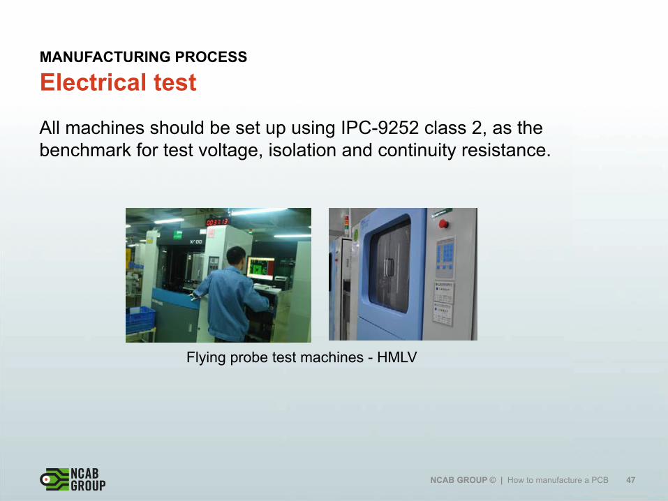
Electrical test MANUFACTURING PROCESS
All machines should be set up using IPC-9252 class 2, as the benchmark for test voltage, isolation and continuity resistance. Flying probe test machines - HMLV
NCAB GROUP © | How to manufacture a PCB 47

FQC / Inspection MANUFACTURING PROCESS
Checking the PCB for acceptance criteria as defined in customer specifications / NCAB general demands / IPC-A-600. Can be carried out thought manual visual inspection and more recently with the aid of AVI (compares PCB to gerber) – but this still relies on inspectors to make judgements as to acceptance and also if boards that deviate, can be repaired or scrapped. AVI can see defects as small as 35um and has a faster checking speed that human eyes. Can cover almost all aspects of acceptance.
Automated Visual Inspection - AVI
NCAB GROUP © | How to manufacture a PCB 48

Testing MANUFACTURING PROCESS
Salt Spray tester
Atomic Adsorption Spectrometer
Impedance Tester XRF RoHS Tester
Thermal Shock Machine
Reflow Oven
TG Tester XRF thickness checker
SIR test system
SEM & EDS
Hot oil tester Machine
Ion Chromatograhy Analyze Machine
NCAB GROUP © | How to manufacture a PCB 49

50
Introduction to multilayer PCB´s Factory Differences

Factory Differences FACTORY DIFFERENCES
So now we understand how a PCB is made. But how are the factories set up? Are they all the same? Do we need different factories for different PCB’s?
NCAB GROUP © | How to manufacture a PCB 51

Factory Differences FACTORY DIFFERENCES
Different technologies will not all be covered in one single factory, quite often they will specialise in certain technologies: -! Single sided -! Double sided -! Multilayer -! Flex / Flex-rigid -! HDI -! IMS -! Military / Automotive / Medical / Aerospace (high demands) Different technologies will often necessitate different standards of equipment – for example a basic single sided factory may not have the necessary equipment to manufacture reliable higher layer count products.
NCAB GROUP © | How to manufacture a PCB 52

Factory Differences FACTORY DIFFERENCES
As with different technologies, different volumes and lead times will necessitate different factories who can cope with such different demands: -! Prototypes
-! Medium volumes
-! High volumes
-! Fast turnaround
-! Asia vs. Europe
NCAB GROUP © | How to manufacture a PCB 53

Factory Differences FACTORY DIFFERENCES
In summary; it is very important to select the right combination of factory setup and match that to the type of the PCB, and also the demand. Get this wrong and results could include: -! The lead times quoted might not match the actual delivery.
-! The quantity delivered might not be full quantity.
-! The factory may not truly have the technical competence to reliably make the board and this might not be apparent upon receipt!
-! The cost may be unnecessary high.
NCAB GROUP © | How to manufacture a PCB 54

Questions?

NCAB GROUP SEMINARS
Improve your knowledge about PCBs – participate in our seminars