Native TestBench Tutorial - pudn.comread.pudn.com/downloads161/ebook/727380/ntb_tutorial.pdfnative...
66
Comments? E-mail your comments about Synopsys documentation to [email protected] Native TestBench Tutorial Version 7.1.1, February 2004
-
Upload
vuongquynh -
Category
Documents
-
view
252 -
download
3
Transcript of Native TestBench Tutorial - pudn.comread.pudn.com/downloads161/ebook/727380/ntb_tutorial.pdfnative...

Native TestBench TutorialVersion 7.1.1, February 2004
Comments?E-mail your comments about Synopsys documentation to [email protected]

Copyright Notice and Proprietary InformationCopyright 2003 Synopsys, Inc. All rights reserved. This software and documentation are owned by Synopsys, Inc., and furnished under a license agreement. The software and documentation may be used or copied only in accordance with the terms of the license agreement. No part of the software and documentation may be reproduced, transmitted, or translated, in any form or by any means, electronic, mechanical, manual, optical, or otherwise, without prior written permission of Synopsys, Inc., or as expressly provided by the license agreement.
Right to Copy DocumentationThe license agreement with Synopsys permits licensee to make copies of the documentation for its internal use only. Each copy shall include all copyrights, trademarks, service marks, and proprietary rights notices, if any. Licensee must assign sequential numbers to all copies. These copies shall contain the following legend on the cover page:
“This document is duplicated with the permission of Synopsys, Inc. for the exclusive use of __________________________________________ and its employees. This is copy number __________.”
Destination Control StatementAll technical data contained in this publication is subject to the export control laws of the United States of America. Disclosure to nationals of other countries contrary to United States law is prohibited. It is the reader’s responsibility to determine the applicable regulations and to comply with them.
DisclaimerSYNOPSYS, INC., AND ITS LICENSORS MAKE NO WARRANTY OF ANY KIND, EXPRESS OR IMPLIED, WITH REGARD TO THIS MATERIAL, INCLUDING, BUT NOT LIMITED TO, THE IMPLIED WARRANTIES OF MERCHANTABILITY AND FITNESS FOR A PARTICULAR PURPOSE.
Registered Trademarks (®)ASYN, CALAVERAS ALGORITHM, CUT THE RISK GET IT RIGHT MAKE IT REAL, DESIGN INSIGHT, DEVICE MODEL BUILDER, EDA WORKSHOP, EDAASSIMILATOR, EDAVALIDATOR, Enterprise, GET REAL. GET ACEO!, HSPICE, HYDRAULICEXPRESS, HYPERMODEL, I, INSPECS, MAST, MASTER TOOLBOX, META, META-SOFTWARE, MODELEXPRESS, Raphael, Saber, TESTIFY, TMA, VERIASHDL, WAVECALC, XYNETIX
Trademarks (™) Active Parasitics, AFGen, Apollo, Apollo II, Apollo-DPII, Apollo-GA, ApolloGAII, ASTRO, Astro-Rail, Astro-Xtalk, ATRANS, Aurora, AvanTestchip, AvanWaves, CALAVARAS, ChipPlanner, Circuit Analysis, Columbia, Columbia-CE, Comet 3D, Cosmos, Cosmos SE, CosmosLE, Cosmos-Scope, Cyclelink, Davinci, DFM-Workbench, Dynamic-Macromodeling, Dynamic Model Switcher, EDAnavigator, Encore, Encore PQ, Evaccess, FASTMAST, Formal Model Checker, FRAMEWAY, GATRAN, Hercules, Hercules-Explorer, Hercules-II, Hierarchical Optimization Technology, High Performance Option, HotPlace, HSPICE-LINK, iQBus, Jupiter, Jupiter-DP, JupiterXT, JupiterXT-ASIC, Libra-Passport, Libra-Visa, LRC, Mars, Mars-Rail, Mars-Xtalk, Medici, Metacapture, Metacircuit, Metamanager, Metamixsim, Milkyway, Nova Product Family, Nova-ExploreRTL, Nova-Trans, Nova-VeriLint, Nova-VHDLlint, Optimum Silicon, Orion_ec, Parasitic View, Passport, Planet, Planet-PL, Planet-RTL, Polaris, Polaris-CBS, Polaris-MT, Progen, Prospector, Proteus OPC, PSMGen, Raphael-NES, Saber Co-Simulation, Saber for IC Design, SaberDesigner, SaberGuide, SaberRT, SaberScope, SaberSketch, Saturn, ScanBand, Silicon Blueprint, Silicon Early Access, SinglePass-SoC, Smart Extraction, SOFTWIRE, Star, Star-DC, Star-Hspice, Star-HspiceLink, Star-MS, Star-MTB, Star-Power, Star-Rail, Star-RC, Star-RCXT, Star-Sim, Star-Sim XT, Star-Time, Star-XP, Taurus, Taurus-Device, Taurus-Layout, Taurus-Lithography, Taurus-OPC, Taurus-Process, Taurus-Topography, Taurus-Visual, Taurus-Workbench, The Power in Semiconductors, THEHDL, TimeSlice, TopoPlace, TopoRoute, True-Hspice, TSUPREM-4, Venus, VERIFICATION PORTAL, VERIVIEW, VFORMAL
SystemC™ is a trademark of the Open SystemC Initiative and is used under license.All other product or company names may be trademarks of their respective owners.
Printed in the U.S.A.Document Order Number 34174-000 SB Native TestBench Tutorial Version 7.1.1, February 2004
ii

Contents
1. Introducing Native TestBench
High-Level Verification . . . . . . . . . . . . . . . . . . . . . . . . . . . . . . . . 1-2
Native TestBench . . . . . . . . . . . . . . . . . . . . . . . . . . . . . . . . . . . . 1-3Concurrency and Control . . . . . . . . . . . . . . . . . . . . . . . . . . . 1-3Random Stimulus Generation with Constraints . . . . . . . . . . 1-4Driving Stimulus and Self-checking . . . . . . . . . . . . . . . . . . . 1-4Interfaces and Clock Domains . . . . . . . . . . . . . . . . . . . . . . . 1-5Classes, Methods and Properties: An Object-Oriented Methodology . . . . . . . . . . . . . . . . . . . . . . . . . . . . . . . . . . . . . 1-5
2. Design Overview
Memory System . . . . . . . . . . . . . . . . . . . . . . . . . . . . . . . . . . . . . 2-1
Tutorial-design Directory Setup . . . . . . . . . . . . . . . . . . . . . . . . . 2-3
3. Arbiter
Arbiter Overview . . . . . . . . . . . . . . . . . . . . . . . . . . . . . . . . . . . . . 3-1
Testbench Overview . . . . . . . . . . . . . . . . . . . . . . . . . . . . . . . . . . 3-3How to Get Going . . . . . . . . . . . . . . . . . . . . . . . . . . . . . . . . . 3-4
Verifying the Arbiter . . . . . . . . . . . . . . . . . . . . . . . . . . . . . . . . . . 3-6
iii

Reset Verification . . . . . . . . . . . . . . . . . . . . . . . . . . . . . . . . . 3-6Simple Request Verification . . . . . . . . . . . . . . . . . . . . . . . . . 3-9Sequenced Request Verification . . . . . . . . . . . . . . . . . . . . . . 3-9Doing Things in an Organized Manner with Tasks . . . . . . . . 3-10
4. Memory Controller
Memory Controller Overview . . . . . . . . . . . . . . . . . . . . . . . . . . . 4-1
Verifying the Memory Controller . . . . . . . . . . . . . . . . . . . . . . . . . 4-4Controller Reset Verification . . . . . . . . . . . . . . . . . . . . . . . . . 4-5Driving the System Bus For Read and Write Operations . . . 4-6Implementing Virtual Ports . . . . . . . . . . . . . . . . . . . . . . . . . . 4-8Verifying Read and Write Operations . . . . . . . . . . . . . . . . . . 4-10
5. Memory System
Memory System Overview . . . . . . . . . . . . . . . . . . . . . . . . . . . . . 5-2
Verifying the Memory System . . . . . . . . . . . . . . . . . . . . . . . . . . . 5-4General Verification . . . . . . . . . . . . . . . . . . . . . . . . . . . . . . . 5-4Object-Oriented Programming . . . . . . . . . . . . . . . . . . . . . . . 5-8Interprocess Communication and Synchronization . . . . . . . . 5-18
iv

1Introducing Native TestBench 1
For quite some time now, design and verification engineers, alike, have felt the need for a single unified platform or environment that allows them to both simulate their HDL designs and verify them with high-level testbench constructs. To this end, Synopsys has integrated a new, efficient, high-performance technology called Native TestBench in its Verilog simulator, VCS. This technology essentially enables engineers to write testbenches in the OpenVera verification language and simulate them in VCS along with their design.
OpenVera was one of Synopsys’ many donations to Accellera (the standards committee for HDL), and is now the basis of System Verilog, the unified design and verification language standard defined by Accellera.
Please contact [email protected] for any questions or issues.
This chapter introduces Native TestBench, followed by a discussion of some of its verification-specific features. It includes the following sections:
• High-Level Verification
• Native TestBench
1-1
Introducing Native TestBench

High-Level Verification
Dramatic increases in the size and complexity of designs, brought about by the internet revolution of the nineties, pose a significant challenge to traditional verification methodologies. The ever-increasing inter-module interactions and design interdependencies have made these verification methodologies inefficient (and in many cases, insufficient) for completing functional validation of designs with the desired degree of confidence and in the allotted amount of time. Therefore, the current need is to provide a means for achieving this functional validation in the most reliable, smart, efficient, and expeditious manner in order to deliver first-time-working silicon or systems on time.
Synopsys has become the leader in providing a single, unified design and verification environment based on VCS that not only enables completing functional validation of designs with the desired degree of confidence, but also helps achieving this goal in the most intelligent and efficient way and in the shortest time possible.
From our experience with customers, the number one objective on the way to reaching this verification goal is to be able to find and fix all bugs in a design before tape-out. The cost of fixing bugs grows exponentially with time as designs evolve. Not catching a few bugs early on in the design process inevitably leads to the dangerous scenario of their proliferation into more bugs, leading to very costly time-delays and design re-spins. In this regard, Synopsys’ unified design and verification environment of VCS is uniquely geared towards catching such hard-to-find bugs efficiently and early in the design cycle. Plus, the tight integration between VCS’s various Smart- verification technologies makes this environment unmatched in its efficiency and speed.
Native TestBench is one of the many key technologies that constitute this environment. Through the use of complex synchronization and timing mechanisms, concurrent processes can be written, providing a mechanism to simulate a real and dynamic test environment. Native TestBench also supports the object-oriented methodology, and provides the necessary abstraction level to develop reliable and reusable test environments. Native TestBench also enables random stimulus generation and self checking, which help increase the efficiency of the verification environment.
1-2
Introducing Native TestBench
Native TestBench
Native TestBench has several features built specifically to address your singular functional verification needs. Please refer to the Native TestBench Language Reference Manual (LRM) for the details on the language syntax, and the Native TestBench User Guide for the usage model.
Concurrency and Control
Concurrency basically allows you to spawn off multiple parallel processes from a parent process. It brings power and flexibility to your verification environment, which inherently requires the execution of many processes in parallel, both for efficiency and smarter inter-process interaction. A typical example would be to stimulate a design and check the outcome in parallel. This allows your testbench to react decisively to the outcome in real time by enabling it to modify the stimulus (even before the simulation ends).
Concurrency is enabled via the fork-join construct, which spawns off multiple parallel processes. The type of join-back to the parent process depends on whether all, any, or none of the parallel processes have completed.
For inter-process communication, constructs called mailboxes allow any process to send a message to any other process. A receiving process can also synchronize with a sending process by waiting for its message.
Constructs called semaphores prevent several parallel processes from trying to access a common resource, such as a signal, by allowing access to only one process at any time.
Constructs called triggers are used in processes to trigger events. These triggered events are received by other processes with the help of constructs called syncs in order to synchronize with the triggering processes.
Other process-control mechanisms are also provided to help processes wait either on specific variables or until the completion of their child processes.
1-3
Introducing Native TestBench

Random Stimulus Generation with Constraints
Verification is primarily concerned with testing unknown, unpredictable corner-case scenarios, as opposed to obvious cases. Random stimulus inherently ensures corner-case scenarios are reached and tested. Thus it ensures that verification time and effort is spent in the most efficient and effective manner.
Native TestBench provides a very powerful mechanism to generate random stimulus. It is based on class-object randomization, which means random variables of a class-object are automatically randomized by a call to the predefined randomize method associated with the object.
Constraints further augment the randomization feature. Constraints are properties that define the boundaries within which the randomization feature works. They have two key advantages: (1) You can add weights so that certain sets of stimuli occur more often than others, that is you can change the distribution function, and (2) you can use the current state of the design to change these weights and consequently the constraints for the next state.
Driving Stimulus and Self-checking
Constructs called drives are used to drive a signal either directly into a design or via its top-level ports.
Similarly, checking the outputs from a design is achieved with constructs called expects which are simple and extremely concise one-line statements.
Expects are advantageous because they automatically cause verification error messages to be displayed when output values do not match expected values. They are designed to catch two typical errors:
• Detecting an expected value at an inappropriate time
• Detecting an unexpected value at any given time
1-4
Introducing Native TestBench
Interfaces and Clock Domains
Interfaces in Native TestBench provide a mechanism to group signals of a design based on design functionality. You can have as many interfaces as needed as long as each is associated with a specific clock. Input signals are driven and output signals are sampled only at clock edges. Interfaces therefore provide separation and clarity between clock domains in a multi-clock design environment.
Classes, Methods and Properties: An Object-Oriented Methodology
You do not need any previous knowledge of or experience with object-oriented methodology in order to use Native TestBench. You will be surprised to discover that object-oriented programming is very similar to HDL programming.
At its very basic level, object-oriented methodology compartmentalizes segments of code into what are called “Classes”. These classes are made up of two entities: “Properties” (data, variables) and “Methods” (function or task routines). Think of a class as an HDL module containing data and behavioral code. A class can be instantiated just like an HDL module with the help of an instance called its “Object”. Methods of this object will operate on class data members and a private data member can only be accessed outside the class by these methods. You can prevent accidental misuse or misapplication of its data in a particular segment of code by specifying methods that limit access to that data. Thus, this methodology provides protection from other code segments that might be using the same data names.
The implementation of object-oriented methodology in Native TestBench is clear, straightforward and elegant, assimilating and extending the best of the features found in C++ and Java. The methodology naturally lends itself to grouping related code and data of a testbench. These groups of data and related code are structured and thus easy to develop, understand, debug, maintain and reuse. The result is a disciplined and systematic testbench structure that is not only useful for verifying small and medium designs, but also has the dramatic, powerful impact on your productivity as soon as designs become large and significantly more complex.
1-5
Introducing Native TestBench

1-6
Introducing Native TestBench

2Design Overview 2
This chapter introduces the design of a system comprising of a memory, an arbiter, a controller, a system bus and CPUs that access the memory, all of which will be used in the remainder of the tutorial. It gives you an overview of the components of the system, describes how they interact with each other to complete the system and details the basic structure of the files used for this tutorial. It includes the following sections:
• Memory System
• Tutorial-design Directory Setup
The files for this tutorial can be accessed in the following directory: $VCS_HOME/doc/examples/nativetestbench.
Memory System
The design used in this tutorial is a simple memory system for a two CPU machine. It consists of a system bus, a centralized round-robin arbiter, and a memory controller that controls four static SRAM devices. Figure 2-1 shows the schematic of this system.
2-1
Design Overview

Figure 2-1 Memory System SchematicNotice that the blocks labeled CPU0 and CPU1 are shaded. This is to indicate that these blocks are not part of the system under test, but rather these blocks will be modeled within the OpenVera testbench. The signals shown between the CPUs and the rest of the system form the interface between the system under test and the “outside world.”
The memory system consists of the SRAMs, the Memory Controller, and the Arbiter. These are all defined in the HDL files of each sub-module. The approach used to verify the memsys system is similar to most project verification flows:
• Initially, all sub-modules are individually verified at the block level.
• Finally, all sub-modules are integrated into the final design for verification at the system level.
This “full chip” functionality is verified at the system level.
SRAM
SRAM
SRAM
SRAM
MEMORYCONTROLLER
System Bus
request[0]
grant[0]
grant[1]
request[1]
ce0_N
ce1_N
ce2_N
ce3_N
addressdata
ROUND-ROBINARBITER
reset
CPU0
CPU1
rdWr_N
2-2
Design Overview

First, in Chapter 3 of the tutorial, the arbiter sub-module is verified. To do this, the surrounding blocks are modeled in the testbench.
Then, in Chapter 4, the memory controller sub-module is verified. For this, both the CPU interface and the memory interfaces are designed in the testbench. This gives you a chance to use some of the advanced features of Native TestBench that could be used to verify protocol based designs.
Finally, Chapter 5 of the tutorial shows you how to verify the complete system by integrating the arbiter and controller sub-modules as shown in the diagram above, with the OpenVera models of the CPUs instantiated in the testbench. Several different features of Native TestBench will be used in different approaches. We will also introduce object-oriented testbench design in this last chapter.
Tutorial-design Directory Setup
The components of the design directory setup are described as follows:
• README — short description and file/directory index and listing of tools and versions used
• sram — contains the memory RTL
• arb — contains the submodule RTL and solution directory
sram arb cntrlr
tutorial
memsys
rtl
sram.v
rtl solution
arb.v
rtl
cntrlr.v
solution
memsys.v
rtl solution
README
testtesttest
2-3
Design Overview

• cntrlr — contains the submodule RTL and solution directory
• memsys — contains the top-level RTL netlist that integrates the entire memsys design and the solution directory
Also note the following:
• Each “rtl” directory contains Verilog HDL code.
• Each “solution” directory contains the solution Native TestBench file, interface, header and script files. Please refer to the “README” file in this directory to see how to run the scripts and see the expected simulation output of the solution files.
• Each “test” directory inside the arb, cntrlr, and memsys directories is where you will be working. You will use this directory for creating your testbench, run scripts, compilation and simulation-generated files and directories.
2-4
Design Overview

3Arbiter 3
This chapter focuses on the arbiter’s role in the design. It briefly describes what the arbiter does, including a short timing and logic discussion. The chapter then describes the Native TestBench technology as it pertains to verifying the arbiter portion of the system. Specifically, this chapter explains how, using this technology, a testbench written in OpenVera interacts with a Verilog design to drive signals, how the connections between the testbench and DUT are made, and how some of the basic signal operations behave. This chapter is divided into the following sections:
• Arbiter Overview
• Testbench Overview
• Verifying the Arbiter
Arbiter Overview
You will be working inside the tutorial/arb/test directory.
• The Verilog arbiter RTL source code is in the following file:
tutorial/arb/rtl/arb.v
3-1
Arbiter

• The solution top-level Verilog is in the following:
tutorial/arb/solution/arb.test_top.v
• The solution testbench is in the following file:
tutorial/arb/solution/arb.vr
• The solution interface is in the following file:
tutorial/arb/solution/arb.if.vrh
• The details of running the solution testbench are in the following file:
tutorial/arb/solution/README
• The solution compile and run scripts are in the following file:
tutorial/arb/solution/run.csh
The timing diagram that describes its IO behavior is now examined. Figure 3-1 shows the timing diagram.
3-2
Arbiter

Figure 3-1 Arbiter Timing Diagram
The arbiter implements a round-robin arbitration algorithm between two CPUs. Each CPU can drive a request input signal (request[0] or request[1]). The arbiter queues the requests and determines which CPU will gain access to the system bus. The arbiter grants this access by asserting one of the grant output signals (grant[0] or grant[1]). While the grant signal is asserted for a given CPU, the CPU continues to assert its request signal so that both the grant and request signals for the CPU remain high while the CPU accesses the system bus. Once the CPU is done, it de-asserts its request signal and, on the subsequent clock cycle, the arbiter de-asserts its grant signal. With all the signals de-asserted, the arbiter can continue with the next request.
Testbench Overview
A testbench suite is comprised of several key components:
• Testbench Module File — Describes the testbench.
• Interface Specification File — Defines the signals for the testbench module. Typically the interface specification is contained in a file with the following name: filename.if.vrh.
• Test_top File (filename.test_top.v) — The top-level Verilog file that encapsulates the DUT and the testbench suite. It instantiates the DUT and the natively compiled testbench (as a shell), and handles system-clock generation and file-dumping in Verilog. Figure 3-2 below shows basic schematic for this configuration.
clk
reset
request[1:0]
grant[1:0]
zz
xx
00 01
1000 00 00 00 00
000000
01
1010 11
01 10
3-3
Arbiter

Figure 3-2 test_top.v Configuration Schematic
How to Get Going
Native TestBench provides a perl script called ntb_template. This script assists in the generation of template files, which help in writing a testbench. Within your working directory (tutorial/arb/test), invoke the template generator in the following manner:
% ntb_template -t arb -c clk ../rtl/arb.v
The -t switch is used to define the top-level name of the circuit under test, which is currently arb. The -c switch defines the clock signal to be used in the generated interface. The specified file (../rtl/arb.v) is the RTL Verilog source code from which the template files are generated. Note that the names of the generated files are derived from the top-level RTL Verilog filename.
Invoking the Native TestBench template generator creates the following template files (you can, alternatively, hand generate any or all of these files):
DeviceUnder Test
Clock Generator
test_top.v file
Input Signals
Testbench
InterfaceRTL Verilog code
(Device Under Test)Output Signals
OpenVera Code
3-4
Arbiter
• arb.test_top.v
• arb.if.vrh
• arb.vr.tmp
arb.test_top.v
The generated arb.test_top.v file contains the top-level Verilog code. The top-level code contains the signal and wire declarations that connect the testbench to the DUT. The declarations are made using the top-level RTL (arb.v). The top-level code also instantiates the testbench (a shell) and the DUT, and contains the clock-generator for the SystemClock (clk) that is passed both to the testbench/interface and the DUT.
arb.if.vrh
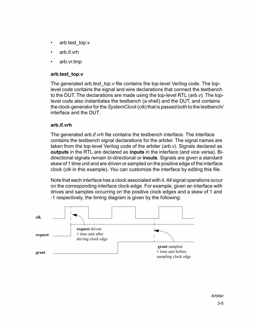
The generated arb.if.vrh file contains the testbench interface. The interface contains the testbench signal declarations for the arbiter. The signal names are taken from the top-level Verilog code of the arbiter (arb.v). Signals declared as outputs in the RTL are declared as inputs in the interface (and vice versa). Bi-directional signals remain bi-directional or inouts. Signals are given a standard skew of 1 time unit and are driven or sampled on the positive edge of the interface clock (clk in this example). You can customize the interface by editing this file.
Note that each interface has a clock associated with it. All signal operations occur on the corresponding interface clock-edge. For example, given an interface with drives and samples occurring on the positive clock edges and a skew of 1 and -1 respectively, the timing diagram is given by the following:
clk
request
grant
request driven1 time unit afterdriving clock edge
grant sampled 1 time unit before sampling clock edge
3-5
Arbiter
arb.vr.tmp
The generated arb.vr.tmp file contains the testbench template file. It also contains the interface-signal macros (explained later) and preprocessor directives that include the arb.if.vrh interface file.
Verifying the Arbiter
First, verify the arbiter’s reset. Then, verify that the arbiter handles simple requests appropriately and can grant access to one of the CPUs. Finally, check for the arbiter’s proper handling of request sequences.
Reset Verification
Verify resets are working correctly. First assert the reset signal. With the reset signal asserted, hold the request signals inactive for each CPU (drive them to 0) and check that the grant signals are at their inactive states (0) after the reset.
Referencing Signals in the Testbench
To reference a signal, specify the interface name and the signal name. Using the arb interface, the reset, request, and grant signals are referenced as:
arb.reset arb.request arb.grant
Basic Signal Operation
All signal operations occur on the clock edge specified in the interface. If an output signal is marked PHOLD, all drives occur on the positive edge of the interface clock. Similarly, input signals marked PSAMPLE are sampled on the positive edge of the interface clock.
To advance the simulation to the next value change of a specified signal, use the synchronize construct:
@(clock_edge signal_name); //clock_edge:posedge/negedge/no edge specified
3-6
Arbiter

This advances the simulation to the specified edge of the signal. If the clock edge is omitted, it advances the simulation to the next signal-value change, which represents a sampling edge.
To assert and de-assert signals, use the Native TestBench drive construct:
@n signal_name = value;
The specified signal is driven to the appropriate value after n clock edges (defined as positive clock edges in the interface in our example). If the delay is omitted, the drive occurs on the next clock edge.
To check that a signal has a specific value at a specified time, use the Native TestBench expect construct:
@n signal_name == value; //other operators except <= allowedThe specified signal is compared to the given value after n clock edges. If the signal value is the same as the specified value, the simulation continues. If there is a mismatch, a verification error occurs with the following error message, but the simulation still continues:
VERIFICATION ERROR: Expect timeout Location: WAIT_ON_EXPECT in program <shell_name>
where shell_name is arb_test in our example.
Generally, it is best to sample input signals slightly before the rising edge of the clock to avoid race conditions. For this purpose, define an input skew of -5 units inside the arb.vr.tmp file by adding the following #define statement to it:
#define INPUT_SKEW #-5
This macro can now be used in the interface definition as the skew value for the PSAMPLE signal declarations. Similarly an appropriate output skew can be defined and used for the output / inout PHOLD signal declarations.
Verifying the Reset
In the arb.vr.tmp file, add the following code to verify the reset:
arb.reset = 1; //assert reset
@2 arb.reset = 0; // de-assert reset after second posedge of clock
@0 arb.request = 2’b00; // de-assert request
@1 arb.grant == 2'b00; //check grant is de-asserted after next posedge
3-7
Arbiter

Note that the request and grant signals are 2-bit signals. Each bit of the signals must be de-asserted.
Compiling and Running the Simulation with VCS
(If you want to run the tutorial solution, go to the arb/solution directory and invoke the script run.csh after making sure you have your $VCS_HOME and license variables already set).
At this point, you should be in the tutorial/arb/test directory. With the code added to your arbiter testbench (arb.vr.tmp), run the simulation and test the results. First, rename arb.vr.tmp to arb.vr.
Compile the testbench use the following VCS command line:
% vcs -ntb arb.test_top.v ../rtl/arb.v arb.vr -Mupdate
This generates the testbench shell called “arb_test” which is internal to VCS.
Run the simulation by simply invoking the VCS executable simv in the following way:
% simv
Any verification errors found during the simulation will be automatically reported. For instance, change the line (expect) that checks the de-assertion of grant in the arb.vr file to the following:
@1 arb.grant == 2’b01;
Recompile and run the simulation again. The testbench now expects the grant signal to be asserted while the Verilog model continues to de-assert the signal as before. This results in an expect mismatch and a verification error as described on the previous page. The simulation will, however, proceed.
Note: Remember to edit the testbench file arb.vr to correct this error before moving ahead with the tutorial.
3-8
Arbiter

Simple Request Verification
To check if the arbiter is handling simple requests correctly, monitor the request signals, check that the grant signal is set appropriately, and then check that the grant signal is de-asserted after the request is released.
Test For Simple Request by CPU0
To test that simple requests are handled correctly for CPU0, drive bit 0 of the request signal and then monitor bit 0 of the grant signal. Finally, de-assert both bits of the request signal and check that both bits of the grant signal are properly de-asserted.
@0 arb.request = 2’b01; // assert bit 0 of request
@2 arb.grant == 2’b01; // check that bit 0 of grant is asserted
@0 arb.request = 2’b00; // de-assert bit 0 of request
@2 arb.grant == 2’b00; // check that both bits of grant are de-asserted
Test For Simple Request by CPU1
To test that simple requests are handled correctly for CPU1, drive bit 1 of the request signal and then monitor bit 1 of the grant signal. Finally, de-assert both bits of the request signal and check that both bits of the grant signal are properly de-asserted.
@0 arb.request = 2’b10; // assert bit 1 of request
@2 arb.grant == 2’b10; // check that bit 1 of grant is asserted
@0 arb.request = 2’b00; // de-assert bit 1' of request
@2 arb.grant == 2’b00; // check that both bits of grant are de-asserted
Sequenced Request Verification
Verify sequences of requests are handled properly by checking a series of conditions:
• Assert both request signals and check that the correct grant is asserted (depends on which grant was previously asserted)
• Release the granted request and check that both grants are released
• Then check that the other grant is asserted
3-9
Arbiter

• Finally release the other request and check that both grants are released
Given this verification methodology, the code to check the arbiter behavior is the following:
@0 arb.request = 2’b11; // assert both request signals @2 arb.grant == 2’b01; // check for first grant @0 arb.request = 2’b10; // de-assert corresponding request @2 arb.grant == 2'b00;// check that grant de-asserts for 1 cycle @1 arb.grant == 2'b10; // check that other grant is asserted @0 arb.request = 2'b00; // de-assert corresponding request @2 arb.grant == 2'b00; // check that both grant signals are de-asserted
Doing Things in an Organized Manner with Tasks
After writing the above pieces of the testbench in the arb.vr file and verifying that they run, you probably have noticed that the simulation takes hardly a fraction of a second to run and complete. Now, you can think of stretching the simulation by checking repeatedly with sequences of reset followed by request. This can be easily done by putting the code for reset and request in tasks and then calling these tasks from the main program in the testbench (arb.vr file).
The following code shows you how to write a task for verifying the reset:
task reset_test () { printf("Task reset_test: asserting and checking
reset\n"); arb.reset = 1; //assert reset @2 arb.reset = 0; // de-assert reset after second posedge @0 arb.request = 2’b00; // de-assert request @1 arb.grant == 2'b00; // check grant is de-asserted
// after next posedge}
You can write a similar task called request_grant_test for verifying the request and grant sequence and then call both the tasks from the main program of the testbench in the following manner:
for (count = 0; count < 2000; count++) {
reset_test();request_grant_test();
}
3-10
Arbiter

4Memory Controller 4
This chapter discusses the memory controller in your design. It gives you an overview of how the memory controller operates. It discusses some of the major features of Native TestBench used to verify the controller, including a description of virtual ports as well as synchronous and asynchronous events. These concepts are presented within the verification framework so that you can learn how to adequately validate the memory controller. This chapter includes the following sections:
• Memory Controller Overview
• Verifying the Memory Controller
Memory Controller Overview
In our system, the CPU accesses the bus through the arbiter. Once the CPU has access, it puts its request on the system bus. The memory controller acts on this request by reading data from the SRAM devices and returning data when necessary. You will be working inside the tutorial/cntrlr/test directory.
• The Verilog controller RTL source code is in the following file:
tutorial/cntrlr/rtl/cntrlr.v
4-1
Memory Controller

• The solution top-level Verilog is in the following file:
tutorial/cntrlr/solution/cntrlr.v
• The solution testbench is in the following file:
tutorial/cntrlr/solution/cntrlr.vr
• The solution interface is in the following file:
tutorial/cntrlr/solution/cntrlr.if.vrh
• The details of running the solution testbench are in the following file:
tutorial/cntrlr/solution/README
• The solution compile and run scripts are in the following file:
tutorial/cntrlr/solution/run.csh
The memory controller reads requests from the system bus and generates control signals for the SRAM devices attached to it. For read requests, the controller reads data and transfers it back to the bus and the CPU making the request. The address bus is 8 bits wide, which creates an address space of 256 bytes. The controller supports up to 4 devices, allocating a maximum of 64 bytes of memory to each. The controller decodes the address and generates the chip enable for the corresponding device during a transaction. Figure 4-1 shows a diagram of how the testbench works with both the system bus and SRAM device signals.
Figure 4-1 Native TestBench/Memory Controller Interaction
Testbench
MEMORYCONTROLLER
rdWr_N
ce2_N
ramData[7:0]
ce3_NbusRdWr_N
busData[7:0]
busAddr[7:0]
adxStrb
reset
ramAddr[5:0]ce0_Nce1_N
4-2
Memory Controller

Figure 4-2 and Figure 4-3 show the timing diagrams for the memory controller’s read and write operations respectively (note the signal names as you will be using them in the verification process).
Figure 4-2 Memory Controller Read Operation Timing Diagram
Note: In the case of cex_N, x refers to 0,1,2 and 3.
clk
reset
adxStr
busAdd
busDat
busRdWr
vali
cex_
ramDat
ramAdd
rdWr
vali
vali
vali
busRdWr_N
cex_N
rdWr_N
cex_N
4-3
Memory Controller
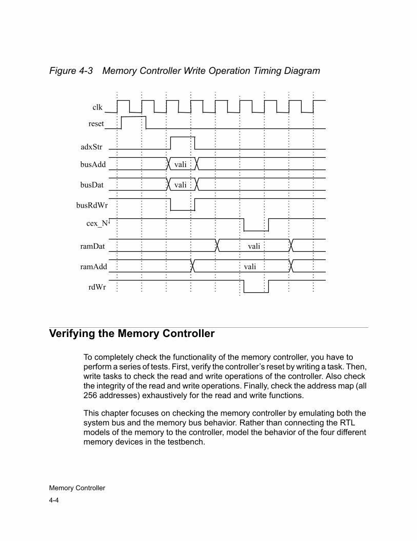
Figure 4-3 Memory Controller Write Operation Timing Diagram
Verifying the Memory Controller
To completely check the functionality of the memory controller, you have to perform a series of tests. First, verify the controller’s reset by writing a task. Then, write tasks to check the read and write operations of the controller. Also check the integrity of the read and write operations. Finally, check the address map (all 256 addresses) exhaustively for the read and write functions.
This chapter focuses on checking the memory controller by emulating both the system bus and the memory bus behavior. Rather than connecting the RTL models of the memory to the controller, model the behavior of the four different memory devices in the testbench.
clk
reset
adxStr
busAdd
busDat
busRdWr
vali
vali
cex_
ramDat
ramAdd
rdWr
vali
vali
cex_Ncex_N
4-4
Memory Controller

To start the verification process, first create the following template files using the template generator as you did in the previous chapter:
• cntrlr.test_top.v (top-level Verilog code)
• cntrlr.vr.tmp (testbench file)
• cntrlr.if.vrh (interface file)
The command line for using the template generator is the following:
% ntb_template -tem -t cntrlr -c clk ../rtl/cntrlr.v
Controller Reset Verification
First assert the reset signal for at least one clock cycle. With the reset signal asserted, check that the memory enable signals are de-asserted.
Resetting the Controller
Using simple drives, create a task as follows and add it to the cntrlr.vr.tmp file to reset the controller:
task resetSequence (){ cntrlr.reset = 1'b1; @2 cntrlr.reset = 1'b0;}
Verifying the Reset
Create another task as follows to verify that the memory enable signals (active_low) for all the 4 SRAM devices are de-asserted (high) and add it to the cntrlr.vr.tmp file:
task resetCheck (){ @0,10 cntrlr.ce0_N == 1'b1; cntrlr.ce1_N == 1'b1; cntrlr.ce2_N == 1'b1; cntrlr.ce3_N == 1'b1;}
4-5
Memory Controller

Invoking the Tasks
Having created the two tasks as described above, write calls to them in the main program in the cntrlr.vr.tmp file as follows:
program cntrlr_test{ @(posedge cntrlr.clk);
resetSequence(); resetCheck();} // end of program cntrlr_test
Compiling and running the Simulation with VCS
At this point, you should be in the tutorial/cntrlr/test directory. With the code added to your controller testbench (cntrlr.vr.tmp), run the simulation and check the results. First, rename cntrlr.vr.tmp to cntrlr.vr.
Compile the testbench using the following VCS command line:
% vcs -ntb cntrlr.test_top.v ../rtl/cntrlr.v cntrlr.vr -Mupdate
This generates the testbench shell called "cntrlr_test" which is internal to VCS.
Run the simulation by simply invoking the VCS executable simv in the following way:
% simv
Driving the System Bus For Read and Write Operations
In testing the read and write capabilities of the controller, create two tasks that drive the bus for read and write operations.
Read Operation
Create a task that drives the read operation onto the system bus as specified in the timing diagram for the controller. The task should use an 8-bit bus address as an input. Given this requirement, the read operation task is the following:
4-6
Memory Controller

task readOp (bit[7:0] adx) {
cntrlr.busAddr = adx; cntrlr.busRdWr_N = 1’b1; cntrlr.adxStrb = 1’b1; @1 cntrlr.adxStrb = 1’b0;
}
This task is passed the argument adx. It then drives the busAddr signal to that value. Finally, it drives the busRdWr_N and adxStrb signals such that they match the timing diagram for the read operation of the controller.
Note: Since this is a read operation, do not drive the data onto the bus and check for the expected data here.
Write Operation
Create a task that drives the write operation onto the system bus as specified in the timing diagram for the controller. The task should use 8-bit address and data busses as inputs. Finally, the task should leave the bus in an idle state (defined when busData is in high z and busRdWr_N is de-asserted). Given these requirements, the write operation task is the following:
task writeOp (bit[7:0] adx, bit[7:0] data) {
@1 cntrlr.busAddr = adx; cntrlr.busData = data; cntrlr.busRdWr_N = 1’b0; cntrlr.adxStrb = 1’b1; @1 cntrlr.busRdWr_N = 1’b1; cntrlr.busData = 8’bzzzzzzzz; cntrlr.adxStrb = 1’b0;
}
This task is passed the argument adx. It then drives the busAddr signal to that value. Finally, it drives the busData, busRdWr_N, and adxStrb signals such that they match the timing diagram for the write operation of the controller.
4-7
Memory Controller

Implementing Virtual Ports
In Native TestBench, a virtual port enables interface signals to be grouped into logical bundles. A virtual port is a set of generic port signal members that act as placeholders for interface signals. When needed, these are bound to specific interface signals. This feature allows a task/function to be written once, but re-used many times with different interfaces of the design under test.
Defining Virtual Ports
Virtual ports are defined outside the main program block using this construct:
port port_name {port_signal_member1; ...; port_signal_memberN;}
port_name Name of the port — must be a valid identifier.
port_signal_memberN Name of the port signal — must be a valid identifier. Multiple port signal names are separated by semi-colons (;).
Binding Virtual Port Signal Members to Interface Signals
The bind construct is used to associate port signal members with interface signals. It defines a global static variable of type port_name to reference the interface signals. Binds are defined outside the main program block.
bind port_name port_variable {
port_signal_member interface_name.signal_name; }
port_name The user-defined virtual port whose signal member names you want associated with interface signals.
port_variable The name of the variable being declared.
port_signal_member The name of the generic signal names you are including in the bind. Generally, all of the signals in the port are bound. However, you can bind selected signals if you want, and leave others unbound.
4-8
Memory Controller

interface_name The name of the interface to which you are binding the port signal members.
signal_name The name of the signal you are binding to a particular port signal member. You can specify signal subfields using signal_name[x:y].
Referencing Ports and Binds
The global static variable defined in the bind construct is not directly passed to tasks/functions. First, a port variable of the same type is declared and intialized to the global static variable.
port_name port_variable = initial_value;
port_name The name of the port data type.
port_variable The name of the port variable you are declaring.
initial_value This is the static port variable defined in the bind construct. If it is not set, the port_variable has a NULL value.
Global static variables defined in binds are passed to tasks/functions via the port variable so that specific interface signals can be referenced and acted upon.
To reference individual interface signals within a tasks/functions, use this construct:
port_variable.$port_signal_member
This references the port signal member that is associated with the interface signal you want acted upon.
Implementing Ports and Binds in the Memory Controller
Given the port/bind methodology presented here, let us define a device port for the SRAM parts (ramAddr, ramData, rdWr_N, and ce_N) as follows:
port device {
4-9
Memory Controller

ramAddr; ramData; rdWr_N; ce_N;
}
After defining the virtual port, connect the port signals to the actual interface signals using the bind construct as follows:
bind device device0 {
ramAddr cntrlr.ramAddr; ramData cntrlr.ramData; rdWr_N cntrlr.rdWr_N; ce_N cntrlr.ce0_N;
}
This bind construct results in the port variable device0 of port type device. It connects the port signals to their corresponding interface signals. Note that the ce_N signal is connected to its device-specific signal. Similar binds for each device (device1, device2, and device3) should be constructed.
Verifying Read and Write Operations
The memory controller issues read and write operations to each of the four SRAM devices as shown in the earlier timing diagram. Create read and write tasks in your testbench that check these operations. Earlier, you modeled the timing diagram exactly, cycle by cycle. Your approach now is to make use of timing windows, which allow you to specify ranges of time and event sequences.
Because of complex timing issues with the read operation, examine the write operation first. A discussion of the timing issues and the read operation follows.
Timing Windows
Native TestBench provides timing windows for its expect constructs. The syntax is the following:
@window signal_name == value;
4-10
Memory Controller

The window of time for which the check is made must be in the form “x,y”. The check begins x clock edges after the current simulation time and continues for y clock edges after the check begins. If the x is omitted, that is, the window of time is of the form “,y”, the check begins immediately and lasts y clock edges after the check begins. However, the check is disabled as soon as the signal value matches the expected value at any time within the window.This mechanism provides a means to evaluate a signal in a specified period of time.
Verifying the Write Operation
To verify the write operation, create a task that checks the SRAM write operation against the timing diagram provided. The task should have the device_id port variable as an argument so that we can pass in the signals on which we want the task to act. The task also has 6-bit address and 8-bit data busses as inputs. It must check that the SRAM signals are driven correctly, check that the address is the right address, and drive the data onto the ramData bus at the appropriate time. Given these requirements, the code for the write operation is the following:
task checkSramWrite (device device_id, bit [5:0] adx, bit [7:0] data) { @1,5 device_id.$ramAddr == adx;
@,2 device_id.$ramData == data;
@1 device_id.$rdWr_N == 1'b0; device_id.$ce_N == 1'b0; device_id.$ramData == data; device_id.$ramAddr == adx;
@1 device_id.$rdWr_N == 1'b1; device_id.$ce_N == 1'b1; device_id.$ramData == data; device_id.$ramAddr == adx;
}
4-11
Memory Controller

The task first checks whether the address (ramAddr) is valid in a timing window that begins after the first rising edge and lasts for the next five rising clock edges. As soon as the address is found to be valid, the task checks whether the data (ramData) to be written is valid in a timing window that begins immediately and lasts for the next two rising clock edges. At the rising edge after the data is found to be valid, the task checks whether the write (rdWr_N) and enable (ce_N) signals are asserted. At the same time, the address and data are checked again to see if they are still valid. Then, after another rising clock edge, the task checks whether the write and enable signals are de-asserted while checking the address and data for the third time to make sure they were valid.
Notice how the task accesses each SRAM instance by binding the port "device" to the interface signals specific to the instance with the help of the task argument device_id. The SRAM instance that is accessed depends on the port variable passed to the task through the argument device_id. For example, if the port variable passed is device0, the fourth statement in the task would be interpreted as cntrlr.ce1_N==1’b0, and so on and so forth.
Synchronous and Asynchronous Timing
By default, all Native TestBench signal operations are synchronous. That is, they occur on the clock edges specified in the interface specification. However, Native TestBench signal operations can be made asynchronous by adding the async keyword after the drive or expect operation as follows:
@(edge signal_name async); //advance to next edge of signal signal_name = value async; // drive new value immediately signal_name == value async;// execute expect expression
// immediately
Note that the delays for the drive and expect operations are not used since they occur immediately.
These are examples of async statements:
@(posedge main_bus.request async);memsys.data[3:0] = 4’b1010 async;data[2:0] = main_bus.data[2:0] async;main_bus.data[7:4] == 4’b0101 async;
4-12
Memory Controller

Verifying the Read Operation
To verify the read operation, check that the control signals are asserted, the correct address is driven by the memory controller, and the input data is driven as return data. However, an interesting timing issue arises in this case. Because of the driving skew, the enable signal is asserted just after the rising clock edge. This means that the data should be drivenimmediately and asynchronously upon sampling the enable signal. This timing diagram shows this behavior:
With this in mind, create a read task that checks the read operation against the timing diagram provided. The task must have the port variable device_id as an argument to allow it to access the enable signal of a particular SRAM instance. It also has 6-bit address and 8-bit data busses as inputs. The code for this task is the following:
task checkSramRead (device device_id, bit [5:0] adx, bit [7:0] data) {
@(device_id.$ce_N async); device_id.$ce_N == 0 async; device_id.$rdWr_N == 1 async; device_id.$ramAddr == adx async; device_id.$ramData = data async;
@1,3 cntrlr.busData == data; device_id.$ramData <= 8'bzzzzzzzz;
}
clk
enable
enable is drivenjust after risingedge
data VALID
data should bedriven here
4-13
Memory Controller

This task first advances the simulation to the change in the SRAM instance enable signal using the asynchronous construct. Next, it immediately checks that enable is 0, rdWr_N is de-asserted, and ramAddr has the appropriate value. After these checks, drive the data (ramData) immediately. Use the async construct here, so that the drive is executed immediately after the checks, and not on the next rising clock edge. Next, check that the system bus has valid data in the specified window of time, which is three cycles after the next rising clock edge. Finally, one rising edge later, drive the data (ramData) back to tri-state (note the use of the <= drive operator, which indicates a non-blocking drive so that execution continues immediately).
Running the Simulation
With the reset check completed, write the code to check the complete write operation of one of the devices. This includes the code to drive the bus for the write operation in the writeOp() task, and the code to check that write operation in the checkSramWrite() task. The code is the following:
writeOp (8’h01, 8’h5A); checkSramWrite (device0, 6’b000001, 8’h5A);
This code drives the bus and then checks the write operation using the specified interface signals associated with device0. When checking other devices, remember that each device has a specific range of valid addresses as shown in the following table:
Device Valid Address Range 0 0-63 1 64-127 2 128-191 3 192-255
Now add in the code to check the write operations for the other devices. The same tasks can be used with different virtual ports and different address parameters.
Similarly, use the generic tasks to drive the bus for read operations and check the device read operations. Remember to check that the returned data matches the return data specified in the timing diagram. The code for these checks is the following:
readOp (8’h03); checkSramRead (device0, 6’b000011, 8’h95);
4-14
Memory Controller

@1 cntrlr.busData == 8’h95;
This code drives the bus and then checks the read operation using the specified interface signals associated with device0 (similar code can be written for the other devices). Finally, the return data is checked to see that it matches the correct value.
These tests only cover a subset of the valid addresses. To exhaustively test the entire range using these calls, each task must be called with every address. This is achieved with the help of a for loop, as shown in the following code:
bit[7:0] index; integer i; ...
for (i=0;i<=255;i++) {
index = i; writeOp(index, 8’h5A);
case (index[7:6]) {
2’b00: device_id = device0; 2’b01: device_id = device1; 2’b10: device_id = device2; 2’b11: device_id = device3;
}
checkSramWrite (device_id, index[5:0], 8’h5A); readOp(index); checkSramRead (device_id, index[5:0], 8’h5A); @1 cntrlr.busData == 8’h5A;
}
Each iteration of this for loop acts on a different address. It drives the bus operation and then checks the SRAM operation using the subroutines defined previously. The case statement changes the interface signals on which the subroutines act so that they correspond to the SRAM instance being accessed. The bus data is then checked at the end of each iteration to monitor the return values.
4-15
Memory Controller

4-16
Memory Controller

5Memory System 5
Now that you’ve become familiar with the separate functionality of the arbiter and memory controller, you can examine the way these components interact in a complete system. This chapter briefly discusses the overview of the system, which includes the arbiter, controller, and SRAM devices.
Also discussed are some of the higher level verification techniques used by Native TestBench. These include concurrency control mechanisms, such as semaphores, triggers, mailboxes, object-oriented methodology by way of classes, and random stimulus generation. Finally, this chapter will show you how to use these features to validate the memory system. This chapter includes the following sections:
• Memory System Overview
• Verifying the Memory System
5-1
Memory System

Memory System Overview
You will be working inside the tutorial/memsys/test directory, which includes the following files:
• The Verilog memory system RTL source code is in the following file:
tutorial/memsys/rtl/memsys.v
• Links to all the RTL for sram, arb, cntrlr and memsys are in the following file:
tutorial/memsys/solution/memsys.f
• The solution top-level Verilog code is in the following file:
tutorial/memsys/solution/memsys.test_top.v
• The solution testbench using is in the following files:
tutorial/memsys/solution/memsys0.vr (semaphores)
tutorial/memsys/solution/memsys1.vr (mailboxes/triggers)
• The solution interface is in the following file:
tutorial/memsys/solution/memsys.if.vrh
• The testbench code that mimics the CPUs is in the following file:
tutorial/memsys/solution/cpu.vr
• The details of running the solution testbench are in the following file:
tutorial/memsys/solution/README
• The solution compile and run script are in the following file:
tutorial/memsys/solution/run.csh
The memory system acts as a wrapper that instantiates the arbiter, memory controller, and four SRAM devices. In our system, the system bus is driven by two separate CPUs, with access granted through the arbiter. The memory controller handles the reading and writing of data to and from the system bus. A schematic of the complete system is provided in Figure 5-1.
5-2
Memory System

Figure 5-1 Memory System Schematic
SRAM
SRAM
SRAM
SRAM
MEMORYCONTROLLER
System Bus
request[0]
grant[0]
grant[1]
request[1]
ce0_N
ce1_N
ce2_N
ce3_N
addressdata
ROUND-ROBINARBITER
reset
CPU0
CPU1
rdWr_N
5-3
Memory System
Verifying the Memory System
The methodology used to verify the entire memory system is broken down by the following tasks and concepts:
• General Verification — Port initialization, reset verification and read/write operations.
• Basic Concurrency and Control — Concurrency between the two CPUs using fork/join, and Control using semaphores to make sure the CPUs do not access the memory at the same time.
• Object-oriented Programming — Object-oriented programming using a Class to model a CPU while making the model re-usable.
• Interprocess Communication — Communication between the two CPUs using Mailboxes and Triggers to make sure that the simulation advances in lock-step fashion.
General Verification
To start the verification process, first create the following template files, as you did in the previous chapter, using the template generator:
• memsys.test_top.v (top-level Verilog code)
• memsys.vr.tmp (testbench file)
• memsys.if.vrh (interface file)
The command line for using the template generator is the follows
% ntb_template -tem -t memsys -c clk ../rtl/memsys.v
Before you write any testbench code, rename the memsys.vr.tmp file to memsys.vr.
The general verification tasks include initializing ports, checking the reset procedure and modifying the read and write operations previously developed for the memory controller. You can do this with the help of tasks. Finally, you can develop a testbench that checks both CPUs being run concurrently using multiple threads.
5-4
Memory System

Port Initialization and Reset Verification
To check that the system is resetting correctly, we must first initialize ports and then go through the reset sequence. The code to do this is the following:
task init_ports () {
@(posedge memsys.clk);memsys.request = 2’b00;memsys.busRdWr_N = 1’b1;memsys.adxStrb = 1’b0;memsys.reset = 1’b0;
}task reset_sequence () {
memsys.reset = 0;@1 memsys.reset = 1;@10 memsys.reset = 0;@1 memsys.grant == 2’b00;
}
Read and Write Operations
The bus used for accessing the memory in the system is very similar to the bus used in the memory controller in the previous chapter. Using this system bus, the writeOp() task for the memory system is the following:
task writeOp (bit[7:0] adx, bit[7:0] data){
@1 memsys.busAddr = adx; memsys.busData = data; memsys.busRdWr_ = 1’b0; memsys.adxStrb = 1’b1; @1 memsys.busRdWr_N = 1’b1; memsys.busData = 8’bzzzzzzzz; memsys.adxStrb = 1’b0;
}
During the read operation, the read operation task must also check for correct return data. The new readOp() task with this data checking is the following:
5-5
Memory System

task readOp (bit[7:0] adx, bit[7:0] data){
@1 memsys.busAddr = adx; memsys.busRdWr_N = 1’b1; memsys.adxStrb = 1’b1; @1 memsys.adxStrb = 1’b0; @2,5 memsys.busData == data;
}
Multiple Threads or Concurrent Processes
Fork/join blocks are the primary mechanism for creating concurrent processes. The syntax to declare a fork/join block is:
fork {statement1;} {statement2;} {...} {statementN;}
join wait_optionstatementN
Can be any valid Native TestBench statement or sequence of statements.wait_option
Specifies when the code after the fork/join block executes. The fork/join block can be either blocking or non-blocking. If it blocks, the code following the fork/join block will not execute until the code inside the fork/join thread returns. The wait_option must be one of the following:all — When this option is used, the code after the fork/join block executes
only after all of the concurrent processes have completed (default)any — When this option is used, the code after the fork/join block executes
right after any concurrent process within the fork/join completes.none — When this option is used, the code after the fork/join block
executes immediately without waiting for any of the fork/join processes to complete.
5-6
Memory System

With the read and write operations defined, you want to set up your testbench such that each CPU issues a series of read and write requests to the memory system with random addresses and data. The two CPUs should operate concurrently or in parallel. Each CPU should use the random() system function to generate random addresses within the valid address space and an 8-bit data type. The CPUs should then request and access the bus, write the data to the bus, and release the bus (check for the release of the grant signal upon bus release). This sequence should be repeated 256 times using the repeat() flow control statement. Given these criteria, the testbench code is the following:
random(12933); // call random with seed fork { // CPU0
repeat(256) {
randVar0 = random(); // get 32 bit random variable address0 = randVar0[13:6]; // get random 8-bit
// address data0 = randVar0[29:22]; // get random 8-bit data @1 memsys.request[0] = 1'b1; // request the bus @2,20 memsys.grant == 2'b01; // check for grant writeOp(address0, data0); // issue write operation @1 memsys.request[0] = 1'b0; // release request @2,20 memsys.grant == 2'b00; // check for release @1 memsys.request[0] = 1'b1; // request again @2,20 memsys.grant == 2'b01; // check for grant readOp(address0, data0); // issue read operation @1 memsys.request[0] = 1'b0; // release request @2,20 memsys.grant == 2'b00; // check for grant
} }
{ // CPU1 repeat(256) {
randVar1 = random(); // get 32 bit random variable address1 = randVar1[13:6]; // get random 8-bit
// address data1 = randVar1[29:22]; // get random 8-bit data @1 memsys.request[1] = 1'b1; // request the bus @2,20 memsys.grant == 2'b10; // check for grant writeOp(address1, data1); // issue write operation @1 memsys.request[1] = 1'b0; // release request @2,20 memsys.grant == 2'b00; // check for release @1 memsys.request[1] = 1'b1; // request again
5-7
Memory System
@2,20 memsys.grant == 2'b10; // check for grant readOp(address1, data1); // issue read operation @1 memsys.request[1] = 1'b0; // release request @2,20 memsys.grant == 2'b00; // check for grant
} } join
This test works well in exhaustively checking the read and write operations for each CPU. However, because the CPUs are operating concurrently, problems can arise when each CPU accesses the same address space with different data. For instance, if CPU0 first writes to an address space and then CPU1 writes to the same address space, the data that CPU0 reads will be different from what it expects (it reads the data that CPU1 wrote). This will result in simulation failure because of the discrepancy between data read and data expected. A solution to this issue is to use basic concurrency control and this is discussed in the section following object-oriented programming and random stimulus generation.
Object-Oriented Programming
Object-oriented programming allows you to develop programs that are easier to debug and reuse by encapsulating related code (subroutines or methods) and data (properties) together into what is called a class. In this section, you will examine how classes can be implemented in our memory system using virtual ports to associate specific interface signals with each object (instance) of a class, how classes are constructed, how concurrency-control is achieved, how concurrent processes communicate and finally how automatic constrained randomization of stimulus is achieved.
Encapsulation
A class is a collection of data and a set of subroutines that act on that data. A class’s data is referred to as properties, and a class’s subroutines are referred to as methods. An instance of a class is called an object, and an object is comprised of the class’s properties and subroutines.
Class properties are instance-specific. Each instance of a class has its own copy of the variables declared in the class definition.
5-8
Memory System

Because multiple instances of classes can exist, when calling a class method, you must identify the instance name for which the method is being called. This is because each method only accesses the properties associated with its object, or instance. So, when calling a method, you must use this syntax:
instance_name.method_name();
Constructors
Objects, or instances, are created when a class is instantiated using the new statement:
class_name instance_name = new;This declaration creates an instance (called instance_name) of the class class_name. When this construction takes place, the method new(), if any exists within the class, is executed. By defining the task new() within a class, you can initialize the class upon construction or instantiation. Further, by passing arguments to the constructor, you can allow for runtime customizing of the object:
class_name instance_name = new(argument1, argument2, ... argumentN);
Using this constructor, the specified arguments are passed to the task new within the class. The conventions for these arguments are the same as those of the usual Native TestBench subroutine calls.
Implementing a Class
In the memsys example, since you have two CPUs (CPU0 and CPU1), you first declare a class called cpu, so that each CPU can be represented by an object of this class. This is done in the following manner:
class cpu {
//properties bus_arb localarb; local integer cpu_id; bit [7:0] address; bit [7:0] data; integer delay;
//methods
5-9
Memory System

task new(bus_arb arb, integer id); task readOp(); task writeOp(); task request_bus(); task release_bus(); task delay_cycle(); task randomize_tb();
}
Interface-Signal Assignment
When implementing object-oriented concepts in your system, you should make specific interface-signal assignments to each instance or object of a class using virtual ports. Since each of the two CPUs is represented by an object of the class cpu and accesses the system bus through the common arbiter, we declare a virtual port bus_arb and then, using it, declare two binds, one for use with each of the two class cpu objects. Thus, we ensure each CPU connects to the arbiter using its specific interface signals. The code for declaring a virtual port is the following:
port bus_arb {
arbreq;arbgrant;
} Using this port declaration, we declare two binds, one for each CPU, as follows:
bind bus_arb arb0 {
arbreq memsys.request[0]; arbgrant memsys.grant[0];
} bind bus_arb arb1 {
arbreq memsys.request[1];arbgrant memsys.grant[1];
}
5-10
Memory System

Depending on the CPU object that is invoked, the bind associated with that object gets passed to its class methods and determines which interface signals get affected.
Class Methods
In your class cpu, you must create the initialization method that is executed when the class is constructed. You must then create the read and write operation methods. It is also helpful to create methods to request and release the bus.
The initialization method should pass in the bind of type bus_arb (as declared above) and assign it to a local property. The code for the initialization method new is the following:
task cpu::new (bus_arb arb, integer id){
integer temp; printf("Constructing new CPU.\n"); localarb = arb; cpu_id = id;
}
The read operation readOp must behave as before. Depending on the object of the class cpu that is invoked, the readOp class method only applies to the CPU associated with that object. The code for the readOp class method is the following:
task cpu::readOp () {
printf("CPU %d readOp: address %h data %h\n", cpu_id, address, data);
@1 memsys.busAddr = address; memsys.busRdWr_N = 1'b1; memsys.adxStrb = 1'b1;@1 memsys.adxStrb = 1'b0; @2,5 memsys.busData == data; printf("READ address = 0%H, data = 0%H \n", address,
data); }
5-11
Memory System

The write operation writeOp must behave as before. Depending on the object of the class cpu that is invoked, the writeOp class method only applies to the CPU associated with that object. The conditional statement inside the method evaluates the local property localarb to which the bind was passed in the initialization process and thus the method is able to print which CPU is writing. The code for the writeOp class method is the following:
task cpu::writeOp() {
printf("CPU %d writeOp: address %h data %h\n", cpu_id, address, data);
@1 memsys.busAddr = address; memsys.busData = data; memsys.busRdWr_N = 1'b0; memsys.adxStrb = 1'b1; @1 memsys.busRdWr_N = 1'b1; memsys.busData = 8'bzzzzzzzz; memsys.adxStrb = 1'b0; if (localarb == arb0)
printf("CPU0 is writing \n"); else if (localarb == arb1)
printf("CPU1 is writing \n"); printf("WRITE address = 0%H, data = 0%H \n", address,
data); }
Our request_bus method must assert the corresponding CPU's request line and then check for the appropriate grant line. This is done with the help of the associated bind, which was passed to the local property localarb. The code for the request_bus class method is the following:
task cpu::request_bus () {
printf("CPU %d requests bus on %0s\n", cpu_id, localarb);
@1 localarb.$arbreq = 1'b1; // request the bus @2,20 localarb.$arbgrant == 1'b1; // check for grant
}
Conversely, our release_bus method must release the corresponding CPU's request line and then check for the release of the appropriate grant line. This is done with the help of the associated bind, which was passed to the local property localarb. The code for the release_bus class method is the following:
5-12
Memory System

task cpu::release_bus () {
printf("CPU %d releases bus on %0s\n", cpu_id, localarb);
@1 localarb.$arbreq = 1'b0; // release the bus @1,2 localarb.$arbgrant == 1'b0; // check for grant
}
Random Stimulus Generation
Like before, you would like to randomize the address that each CPU uses when accessing the SRAM. However, this time you will implement the random stimuli for the address with a class method. You also want to introduce a randomized delay between CPU accesses, and further want to constrain this delay to within 10 clock cycles. So you also generate this constrained, randomized delay using modulo arithmetic with this class method. This is demonstrated by the following code for the randomize_vlite() class method:
task cpu::randomize_vlite () {
bit [31:0] random_val;random_val = random();address = random_val[7:0];data = random_val[15:8];delay = {random_val[31:16] % 10}; // random delay with
// constraintprintf("CPU %d randomize_vlite: address %0h data %0h
delay %0d \n", cpu_id, address, data, delay);}
Finally, you write the method delay_cycle() to introduce the delay between CPU accesses. The code for the delay_cycle class method is the following:
task cpu::delay_cycle() { printf("CPU %d Delay cycle value: %d\n", cpu_id, delay); repeat(delay) @(posedge memsys.clk); printf("delay = %d\n",delay);}
5-13
Memory System
Implementing Object-Oriented Programming
Before we can use our objects, we must instantiate each cpu class object and invoke our initialization routines, which specify the interfaces to be used by the objects, in the following manner:
cpu cpu0 = new (arb0, 0);cpu cpu1 = new (arb1, 1);
With your class cpu defined with the properties and methods described above, the same concurrent execution sequences for the two CPUs created earlier using fork/join can now be written as follows:
fork //fork CPU 0{
repeat(256) {
cpu0.randomize_vlite();cpu0.request_bus();cpu0.writeOp();cpu0.release_bus();cpu0.request_bus();cpu0.readOp();cpu0.release_bus();cpu0.delay_cycle();
}}
//fork CPU 1{repeat(256) {
cpu1.randomize_vlite();cpu1.request_bus();cpu1.writeOp();cpu1.release_bus();cpu1.request_bus();cpu1.readOp();cpu1.release_bus();cpu1.delay_cycle();
}}join
5-14
Memory System

Note how the class property address is passed (using the instance name). Also, note the ease of reuse through invoking the class methods with the appropriate instance name.
Basic Concurrency Control
The two objects of the class cpu that were invoked concurrently in the previous subsection have the potential to access the same location in the SRAM memory if the random addresses generated for them happen to be the same. To prevent a potential conflict between the two cpu objects from leading to a data or resource hazard, concurrency control can be achieved using semaphores.
Semaphores
Conceptually, a semaphore is like a bucket containing a number of keys. No process can execute without first obtaining a key. Therefore only as many processes as there are keys can execute at any time. All other processes must wait until the keys are returned.
To allocate a semaphore, you must use the alloc() system function as follows:
function integer alloc(SEMAPHORE, integer semaphore_id, integer semaphore_count, integer key_count);
semaphore_id This is the ID number of the particular semaphore being created. It must be an integer. You should use 0, for the ID is then automatically generated by the simulator. Any other number explicitly assigns that number as the ID to the generated semaphore.
semaphore_count This specifies the number of semaphores (buckets) you want to create. It must be an integer.
key_count This specifies the number of keys initially allocated to each semaphore. It must be an integer.
The alloc() function returns the base semaphore ID if the semaphores are successfully created. Otherwise, it returns 0.
To obtain a key, you must use the semaphore_get() system task/function.
5-15
Memory System

The prototype is:
task | function semaphore_get( integer wait_option , integer semaphore_id, integer key_count);
wait_option The value of option must be one of the following predefined constants:
semaphore_id This ID specifies the semaphore from which to get keys.
key_count This specifies the number of keys being taken from the semaphore.
To return a key, you must use the semaphore_put() system task as follows:
task semaphore_put(integer semaphore_id, integer key_count);
semaphore_id This ID specifies the semaphore to which to returns keys.
key_count This specifies the number of keys being returned to the semaphore.
Subroutine type
Constant Description
Function NO_WAIT This option specifies that the process will not wait for keys if there are no keys available and code execution will continue. Returns a 1 if there is a key, 0 otherwise.
Task WAIT This options specifies that the process will stop further code excution to wait for keys.
5-16
Memory System

Implementing Semaphores
The fork/join code that you wrote earlier should now be modified to include semaphores as follows:
integer semaphoreId; semaphoreId = alloc(SEMAPHORE, 0, 1, 1);fork{// fork process for CPU 0
repeat(256) {
cpu0.randomize_vlite();semaphore_get(WAIT, semaphoreId, 1);cpu0.request_bus();cpu0.writeOp();cpu0.release_bus();cpu0.request_bus();
cpu0.readOp();cpu0.release_bus();semaphore_put(semaphoreId, 1);cpu0.delay_cycle();
}}
{// fork process for CPU 1repeat(256) {
cpu1.randomize_vlite(); semaphore_get(WAIT, semaphoreId, 1); cpu1.request_bus(); cpu1.writeOp(); cpu1.release_bus(); cpu1.request_bus(); cpu1.readOp(); cpu1.release_bus(); semaphore_put(semaphoreId, 1); cpu1.delay_cycle();
}}join
5-17
Memory System

Interprocess Communication and Synchronization
Up until now, you had both CPUs operating concurrently, with each going through the read and write cycles completely. Now, you may want to do things slightly differently by making CPU0 only write to the memory and CPU1 only read from the memory.
However, you must ensure that CPU0 writes before CPU1 reads and that the address generated by CPU0 is passed on to CPU1. Also, the data generated by CPU0 has to be passed on to CPU1 so that it can check for memory corruption by comparing the data read from the memory with that passed to it by CPU0. This interprocess communication in which CPU0 passes the address and data to the waiting CPU1 can be achieved with mailboxes. Further, you must also ensure that CPU1 finishes with its read operation and checks completely before CPU0 starts its next write cycle. This final synchronization can be achieved with triggers and syncs.
Mailboxes
A mailbox is a mechanism to exchange messages between processes. Data can be sent to a mailbox by one process and retrieved by another. Conceptually, mailboxes behave like real mailboxes. When a letter is delivered and put into the mailbox, you can retrieve the letter (and any data stored within). However, if the letter has not been delivered when you check the mailbox, you must choose whether to wait for the letter or retrieve the letter on subsequent trips to the mailbox. Similarly, Native TestBench’s mailboxes allow you to transfer and retrieve data in a very controlled manner.
To allocate a mailbox, you must use the alloc() system function. The prototype is:
function integer alloc(MAILBOX, int mailbox_id, int mailbox_count);
mailbox_id The ID number of the particular mailbox being created. It must be an integer value. You should generally use 0. When you use 0, Native TestBench automatically generates a mailbox ID.
mailbox_count Specifies how many mailboxes you want to create. It must be an integer value.
5-18
Memory System
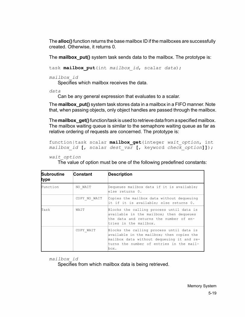
The alloc() function returns the base mailbox ID if the mailboxes are successfully created. Otherwise, it returns 0.
The mailbox_put() system task sends data to the mailbox. The prototype is:
task mailbox_put(int mailbox_id, scalar data);mailbox_id
Specifies which mailbox receives the data.data
Can be any general expression that evaluates to a scalar. The mailbox_put() system task stores data in a mailbox in a FIFO manner. Note that, when passing objects, only object handles are passed through the mailbox.
The mailbox_get() function/task is used to retrieve data from a specified mailbox. The mailbox waiting queue is similar to the semaphore waiting queue as far as relative ordering of requests are concerned. The prototype is:
function|task scalar mailbox_get(integer wait_option, int mailbox_id [, scalar dest_var [, keyword check_option]]);wait_option
The value of option must be one of the following predefined constants:
mailbox_id Specifies from which mailbox data is being retrieved.
Subroutine type
Constant Description
Function NO_WAIT Dequeues mailbox data if it is available; else returns 0.
COPY_NO_WAIT Copies the mailbox data without dequeuing it if it is available; else returns 0.
Task WAIT Blocks the calling process until data is available in the mailbox; then dequeues the data and returns the number of en-tries in the mailbox.
COPY_WAIT Blocks the calling process until data is available in the mailbox; then copies the mailbox data without dequeuing it and re-turns the number of entries in the mail-box.
5-19
Memory System

dest_var The destination variable of the mailbox data.
check_option An optional argument that should be set to CHECK when used. It specifies whether type checking occurs between the mailbox data and the destination variable.
The mailbox_get() system task/function assigns any data stored in the mailbox to the destination variable and returns the number of entries in the mailbox, including the entry just received. If there is a type mismatch between the data sent to the mailbox and the destination variable, a runtime error occurs unless the CHECK option is used. If the CHECK option is active, a -1 is returned, and the message is left in the mailbox and is dequeued on the next mailbox_get() function call. If the mailbox is empty, the function waits for a message to be sent, depending on the wait option. If the wait option is NO_WAIT, the function returns a 0. If no destination variable is specified, the function returns the number of entries in the mailbox, but it does not dequeue an item from the mailbox.
Synchronization Between Concurrent Processes
Concurrent processes can be synchronized with each other using triggers and syncs. First, an event variable is declared. This event is then passed by one of the processes using a trigger. Synchronization of the other process to the one is achieved by using a sync.
Event Variables serve as the link between triggers and syncs. They are bi-directional as they can be used both to pass and receive triggers.
Triggers are used to pass or send events. A trigger is initiated by making a call to the system task trigger defined as follows:
task trigger (ON/OFF, event_name);
event_name is the name of the event that is to be passed. More than one event can be passed by any trigger.
The argument ON or OFF refers to the triggering on or off of the event. Please refer the Native TestBench LRM for other argument options instead of ON.
Syncs are used to receive events and thereby synchronize the receiving processes with the triggering processes. A sync is initiated by making a call to the system task sync defined as follows:
5-20
Memory System

task sync (ALL, event_name);
event_name
event_name is the name of the event that is to be received.More than one event can be received by any sync.
The argument ALL refers to the receiving of all events listed as arguments to the sync. Please refer the Native TestBench LRM for other argument options instead of ALL.
Implementing Interprocess Communication and Synchronization
In order to avoid any conflicts between the two class cpu objects, the fork/join construct that was seen earlier is modified with the help of a mailbox, a trigger and a sync. Now, both objects CPU0 and CPU1 access the same memory location using the random address generated by CPU0. However, they do so not at the same time. While CPU0 writes to a random memory location, CPU1 waits for that random address and the data to be passed to it by CPU0 through a mailbox. CPU1 then accesses the same memory location to read the data. Like wise, CPU0 waits to sync on a triggered event from CPU1 which indicates CPU1 has finished its write cycle and therefore CPU0 can start its next write cycle.
integer mboxId; event CPU1done; mboxId = alloc(MAILBOX, 0, 1); fork {// fork process for CPU 0
repeat(256) {
cpu0.randomize_vlite(); cpu0.request_bus(); cpu0.writeOp(); cpu0.release_bus(); mailbox_put(mboxId, cpu0.address); sync(ALL, CPU1done); trigger(OFF, CPU1done); cpu0.delay_cycle();
} }
{// fork process for CPU 1 repeat(256)
5-21
Memory System

{ mailbox_get(WAIT, mboxId, cpu1.address, CHECK); cpu1.request_bus(); cpu1.readOp(); cpu1.release_bus(); trigger(ON, CPU1done); cpu1.delay_cycle();
} } join
Constrained Randomization of Stimulus
Previously, you had generated the data, address and delay properties of the class cpu using the random() function. Now, you will learn to do the same using the powerful automatic randomization feature of Native TestBench. Further, you will also learn how to specify constraints to automatically constrain certain random properties (variables).
You can declare class properties as random using the rand declaration:
rand data_type variable = initial_value;Variables declared as random within a class are randomized when the randomize() system function is called. Because randomize() acts as a class method, you must specify the instance for which the system function is called:
function int object_name.randomize();object_name
The name of the object in which the random variables have been declared.The randomize() class method generates random values for all random variables within the specified class instance. The randomize() method returns a 1 if it successfully sets all the random variables and objects to valid values. If it does not, it returns a 0. If an object has no random variables anywhere in its inheritance hierarchy (no random variables or sub-objects) or if all of its random variables are inactive, the randomize() function returns a 1.
Using random declarations, we declare our class properties address, data and delay as random as follows:
randc bit[7:0] address;rand bit[7:0] data;rand integer delay;
5-22
Memory System

Each time an instance is randomized, the address, data and delay values for that instance are randomized. In particular, address has to be declared cyclic random (randc), for we want it to cycle through all the 256 memory addresses without repetition.
Note that there are no restrictions on the value that delay can assume because it is declared as a random integer. We can implement constraints on the values that random variables can assume using the constraint construct:
constraint constraint_name { contraint_expressions }constraint_name
The name of the constraint block.constraint_expression
The conditional expression that limits random values. It is a series of expressions that are enforced when the class is randomized.
To limit the values of delay to those between 0 and 10, we define this constraint within the class:
constraint del_lt10 {
delay < 10; delay >=0;
}
Implementing Constraints and Randomization
First, introduce the changes described in the previous subsection in the declaration of the cpu class. This also involves removing the randomize_vlite() class method. The cpu class would now appear as the following:
class cpu {
//properties bus_arb localarb; local integer cpu_id; randc bit [7:0] address; rand bit [7:0] data; rand integer delay;
constraint del_lt10 {
delay < 10;
5-23
Memory System

delay >= 0; }
//methods task new(bus_arb arb, integer id); task readOp(); task writeOp(); task request_bus(); task release_bus(); task delay_cycle();
}
Now, make changes to just one statement inside the fork-join construct from the subsection on "Implementing Interprocess Communication and Synchronization". The task call to the randomize_vlite() class method is to be changed to a system call to the predefined system class method randomize to automatically randomize all variables declared as rand in the declaration of the cpu class. Any constraints defined on the rand variables are also automatically taken into account when randomizing those variables. With these changes, the fork-join construct will appear as the following:
integer mboxId, randflag; event CPU1done; mboxId = alloc(MAILBOX, 0, 1); fork {// fork process for CPU 0
repeat(256) {
randflag = cpu0.randomize(); cpu0.request_bus(); cpu0.writeOp(); cpu0.release_bus(); mailbox_put(mboxId, cpu0.address); sync(ALL, CPU1done); trigger(OFF, CPU1done); cpu0.delay_cycle();
} } {// fork process for CPU 1
repeat(256) {
mailbox_get(WAIT, mboxId, cpu1.address, CHECK);
5-24
Memory System

cpu1.request_bus(); cpu1.readOp(); cpu1.release_bus(); trigger(ON, CPU1done); cpu1.delay_cycle();
} } join
Finally, you can structurally make your code look more elegant by encasing the code for the fork/join in a task called check_all and then calling this and other tasks from inside the program memsys_test in the memsys.vr file as follows:
program memsys_test { // Start of memsys_test
cpu cpu0 = new (arb0, 0); cpu cpu1 = new (arb1, 1);
init_ports(); reset_sequence(); check_all();
} // end of program memsys_test
5-25
Memory System

5-26
Memory System