![NASA Standards Mechanical tests – Strength – Sinusoidal sweep vibration (5 to 50 hertz [Hz]) ELV and STS payloads – Random vibration and acoustics – Shock.](https://static.fdocuments.net/doc/165x107/56649cff5503460f949cfe0b/nasa-standards-mechanical-tests-strength-sinusoidal-sweep-vibration.jpg)
NASA-DOD LEAD-FREE ELECTRONICS PROJECT: VIBRATION TEST · NASA-DOD LEAD-FREE ELECTRONICS PROJECT:...
32
NASA-DOD LEAD-FREE ELECTRONICS PROJECT: VIBRATION TEST Thomas A. Woodrow, Ph.D. Boeing Research and Technology Seattle, WA [email protected] ABSTRACT Vibration testing was conducted by Boeing Research and Technology (Seattle) for the NASA-DoD Lead-Free Electronics Solder Project. This project is a follow-on to the Joint Council on Aging Aircraft/Joint Group on Pollution Prevention (JCAAlJG-PP) Lead-Free Solder Project which was the first group to test the reliability of lead-free solder joints against the requirements of the aerospace/mi Ii tary communi ty. Twenty seven test vehicles were subjected to the vibration test conditions (in two batches). The random vibration Power Spectral Density (PSD) input was increased during the test every 60 minutes in an effort to fail as many components as possible within the time allotted for the test. The solder joints on the components were electrically monitored using event detectors and any solder joint failures were recorded on a Labview-based data collection system. The number of test minutes required to fail a given component attached with SnPb solder was then compared to the number of test minutes required to fail the same component attached with lead-free solder. A complete modal analysis was conducted on one test vehicle using a laser vibrometer system which measured velocities, accelerations, and displacements at one . hundred points. The laser vibrometer data was used to determine the frequencies of the major modes of the test vehicle and the shapes of the modes. In addition, laser vibrometer data collected during the vibration test was used to calculate the strains generated by the first mode (using custom software). After completion of the testing, all of the test vehicles were visually inspected and cross sections were made. Broken component leads and other unwanted failure modes were documented. Key Words: vibration, lead-free solder, NASA, reliability INTRODUCTION The NASA-DoD Lead-Free Electronics Project was started in 2006 to determine whether lead-free solders and finishes (before and after rework) are suitable for use in high reliability electronics. The Project is managed by NASA. The NASA-DoD Lead-Free Electronics Project includes members from the U.S. Air Force, BAE Systems, Boeing, Celestica, Harris, Lockheed Martin, NASA, NA VSEA Warfare Centers (Crane), Raytheon, Rockwell- Collins, ACI, Lockheed Martin, and Texas Instruments, among others. This project is a follow-on to the 2001 Joint Council on Aging Aircraft/Joint Group on Pollution Prevention (JCAA/JG-PP) Lead-Free Solder Project which was the first group to test the reliability of lead-free solder joints against the requirements of the aerospace/military community. The Project members wrote a Project Plan [I] which describes the assembly of the test vehicles and the testing to be done. The testing includes thermal cycling, vibration, mechanical shock, combined vibration/thermal cycling, and copper dissolution testing. The objective of this study was to determine the effects of random vibration on the relative reliability of as-assembled and reworked lead-free and tin/lead solder joints (i.e., which solder survived the longest). Modal data and strain data were also collected during this study in an effort to provide data that would be useful to those that may want to try to model the behavior of the NASA-DoD test vehicle. APPROACH The test vehicle designed for this project was a six-layer circuit board 12.75 inches wide by 9 inches high by 0.090 inches thick (32.39 cm by 22.86 cm by 0.23 cm) (Figure 1) . The design used 0.5 ounce copper and a laminate with a high glass transition temperature (Tg of 170 degrees C, Isola 370HR). The test vehicle was populated with 63 components consisting of ceramic leadless chip carriers (CLCC's), QFN's, Alloy 42 TSOP's, TQFP's, BGA's, CSP's, and PDIP's. The components contained internal wire bonds so that once mounted on the test vehicle, each component would complete an electrical circuit that could be monitored during testing. Failure of a solder joint would cause a break in the electrical circuit that could be detected by an event detector. Each test vehicle also had a daisy-chain of twelve 0.016 inch (0.041 cm) diameter plated through holes so that the reliability of the holes could be determined. The plated through holes were filled with solder during the wave solder operation. Each component location on the test vehicles was given a unique reference designator number. The solder alloys selected for test were: Sn3.0AgO.5Cu paste for reflow soldering (abbreviated as SAC305) https://ntrs.nasa.gov/search.jsp?R=20100029736 2018-05-28T05:14:57+00:00Z
Transcript of NASA-DOD LEAD-FREE ELECTRONICS PROJECT: VIBRATION TEST · NASA-DOD LEAD-FREE ELECTRONICS PROJECT:...

NASA-DOD LEAD-FREE ELECTRONICS PROJECT: VIBRATION TEST
Thomas A. Woodrow, Ph.D. Boeing Research and Technology
Seattle, WA [email protected]
ABSTRACT Vibration testing was conducted by Boeing Research and Technology (Seattle) for the NASA-DoD Lead-Free Electronics Solder Project. This project is a follow-on to the Joint Council on Aging Aircraft/Joint Group on Pollution Prevention (JCAAlJG-PP) Lead-Free Solder Project which was the first group to test the reliability of lead-free solder joints against the requirements of the aerospace/mi Ii tary communi ty.
Twenty seven test vehicles were subjected to the vibration test conditions (in two batches). The random vibration Power Spectral Density (PSD) input was increased during the test every 60 minutes in an effort to fail as many components as possible within the time allotted for the test.
The solder joints on the components were electrically monitored using event detectors and any solder joint failures were recorded on a Labview-based data collection system. The number of test minutes required to fail a given component attached with SnPb solder was then compared to the number of test minutes required to fail the same component attached with lead-free solder.
A complete modal analysis was conducted on one test vehicle using a laser vibrometer system which measured velocities, accelerations, and displacements at one
. hundred points. The laser vibrometer data was used to determine the frequencies of the major modes of the test vehicle and the shapes of the modes. In addition, laser vibrometer data collected during the vibration test was used to calculate the strains generated by the first mode (using custom software).
After completion of the testing, all of the test vehicles were visually inspected and cross sections were made. Broken component leads and other unwanted failure modes were documented.
Key Words: vibration, lead-free solder, NASA, reliability
INTRODUCTION The NASA-DoD Lead-Free Electronics Project was started in 2006 to determine whether lead-free solders and finishes (before and after rework) are suitable for use in high reliability electronics. The Project is managed by NASA. The NASA-DoD Lead-Free Electronics Project includes members from the U.S. Air Force, BAE Systems,
Boeing, Celestica, Harris, Lockheed Martin, NASA, NA VSEA Warfare Centers (Crane), Raytheon, RockwellCollins, ACI, Lockheed Martin, and Texas Instruments, among others. This project is a follow-on to the 2001 Joint Council on Aging Aircraft/Joint Group on Pollution Prevention (JCAA/JG-PP) Lead-Free Solder Project which was the first group to test the reliability of lead-free solder joints against the requirements of the aerospace/military community.
The Project members wrote a Project Plan [I] which describes the assembly of the test vehicles and the testing to be done. The testing includes thermal cycling, vibration, mechanical shock, combined vibration/thermal cycling, and copper dissolution testing.
The objective of this study was to determine the effects of random vibration on the relative reliability of as-assembled and reworked lead-free and tin/lead solder joints (i.e., which solder survived the longest). Modal data and strain data were also collected during this study in an effort to provide data that would be useful to those that may want to try to model the behavior of the NASA-DoD test vehicle.
APPROACH The test vehicle designed for this project was a six-layer circuit board 12.75 inches wide by 9 inches high by 0.090 inches thick (32.39 cm by 22.86 cm by 0.23 cm) (Figure 1) . The design used 0.5 ounce copper and a laminate with a high glass transition temperature (Tg of 170 degrees C, Isola 370HR). The test vehicle was populated with 63 components consisting of ceramic leadless chip carriers (CLCC's), QFN's, Alloy 42 TSOP's, TQFP's, BGA's, CSP's, and PDIP's. The components contained internal wire bonds so that once mounted on the test vehicle, each component would complete an electrical circuit that could be monitored during testing. Failure of a solder joint would cause a break in the electrical circuit that could be detected by an event detector. Each test vehicle also had a daisy-chain of twelve 0.016 inch (0.041 cm) diameter plated through holes so that the reliability of the holes could be determined. The plated through holes were filled with solder during the wave solder operation. Each component location on the test vehicles was given a unique reference designator number.
The solder alloys selected for test were:
Sn3.0AgO.5Cu paste for reflow soldering (abbreviated as SAC305)
https://ntrs.nasa.gov/search.jsp?R=20100029736 2018-05-28T05:14:57+00:00Z

SnO.7CuO.05Ni for wave soldering and as a paste for reflow soldering (abbreviated as SN I OOC) Sn37Pb for reflow and wave soldering (abbreviated as SnPb) Sn4.0AgO.5Cu for BGA balls (abbreviated as SAC405) Snl.OAgO.5Cu for CSP balls (abbreviated as SACI05)
The SAC305 alloy was chosen because it is currently the preferred alloy for use in lead-free commercial electronics. The SN I OOC alloy was chosen because it has been widely used in Asia with good results. SAC405 and SAC 105 are alloys commonly used in the balls on area array devices. Finally, eutectic SnPb was included to act as the control alloy.
The test vehicles were divided into two types, i.e., "Manufactured" test vehicles and "Rework" test vehicles. Both types were made using an immersion silver board finish (although an ENIG PWB finish was used on a few of the test vehicles). The lead-free "Manufactured" and "Rework" test vehicles were assembled using lead-free solders and lead-free reflow and wave soldering profiles. The SnPb "Manufactured" and "Rework" test vehicles were assembled using eutectic SnPb solder and SnPb reflow and wave soldering profiles and were used as the controls. A 5-mil laser cut stencil was used during paste application.
As the name suggests, selected components on the "Rework" test vehicles were reworked. The components were removed; residual solder was cleaned from the pads using solder wick; and new components were attached using either SnPb or lead-free solder.
The "Rework" test vehicles were also populated with a number of mixed technology components (i.e., SnPb paste combined with a lead-free component finish or lead-free paste combined with a SnPb component finish) ..
The CLCC's with a lead~free pad finish were produced by dipping of gold-plated CLCC's into the respective molten solders. In addition, some tin-plated TQFP's were dipped into either molten SnPb or molten SAC305 to simulate a tin whisker mitigation process.
The component finishes used included SnPb, matte Sn, SnBi, SAC305, SAC405, and SACl05.
Table 1 lists the components used on the SnPb and leadfree "Manufactured" test vehicles; the finish on each component; and the solders used. .
Table 2 lists the components used on the SnPb and leadfree "Rework" test vehicles; the finish on each component; the solders used; and which components were actually reworked.
. One hundred and ninety three' test vehicles were assembled at BAE Systems in Irving, TX. One hundred
and twenty of these test vehicles were "Manufactured" PWA's and seventy three were "Rework" PWA's. Eighteen components were reworked on each of the "Rework" test vehicles (six BGA's; six CSP's; two PDIP's; and four TSOP's). In general, solder wire was used for reworking the components. The BGA's and CSP's, however, were replaced using flux only or by applying paste to the balls and then using a hot air rework station to form the solder joints (see Table 2). During rework of the BGA's and CSP's, a SnPb thermal profile was used for the SnPb "Rework" test vehicles and a Pb-free thermal profile was used on the Pb-free "Rework" test vehicles. The reflow profiles for initial assembly using either SnPb or the lead-free solder pastes are shown in Figures 2 and 3. The wave soldering profiles used for tin/lead and lead-free wave soldering can be found in [2]. Wave soldering with SnPb was done at BAE Systems and the lead-free wave soldering was done at Scorpio Solutions in Garfield Heights, Ohio. The rework profiles for removing and replacing the BGA's and the CSP's using a hot air rework station can also be found in [2]. All rework was done at BAE Systems, Lockheed Martin, and Rockwell-Collins. Each rework site focused on the test vehicles for a specific test to eliminate effects due to site-to-site variations in rework procedures.
After assembly and rework, all test vehicles were thermally aged at 100°C for 24 hours. Twenty seven test vehicles were then delivered to Boeing for mechanical shock testing. These consisted of 5 SnPb "Manufactured" test vehicles; 6 Pb-free "Manufactured" test vehicles assembled with SAC305 paste; 5 Pb-free "Manufactured" test vehicles assembled with SNIOOC paste; 6 SnPb "Rework" test vehicles; and 5 Pb-free "Rework" test vehicles. AIl of the test vehicles had an immersion silver PWB finish except for one SAC305 "Manufactured" test vehicle (Test Vehicle 96) and one SnPb "Rework" test vehicle (Test Vehicle 157) which had an ENIG PWB finish.
On the SnPb "Rework" test vehicles, all of the CLCC's were finished with SAC305 (on the pads and in the castellations) and assembled with SnPb paste which resulted in lead-free solder joints contaminated with Pb after assembly (see Table 2). In addition, some of the BGA's combined SAC405 balls with SnPb solder paste which resulted in lead-free solder joints contaminated with Pb (on reworked and unreworked BGA's). Also, some of the CSP's combined SACl05 balls with SnPb solder paste (reworked and unreworked). This mixing was done intentionally in order to determine the effects of lead-contamination upon lead-free solder reliability. Inductively coupled plasma (ICP) spectroscopy was used by Boeing to quantify the amount of Pb in these solderjoints on one of the SnPb "Rework" test vehicles (see Table 3; Test Vehicle 10 # 149). The solder joints were removed with a scalpel, dissolved in mixed nitriclhydrochloric acid, and the solution was analyzed by ICP spectroscopy.
On the Pb-free "Rework" test vehicles, all of the CLCC's and QFN's were finished with SnPb and assembled with SAC305 paste which resulted in lead-free solder joints contaminated with Pb after assembly (see Table 2). In addition, some of the BGA's combined SnPb balls with SAC305 solder paste which
1 I

resulted in lead-free solder joints contaminated with Pb (on unreworked BGA's). Also, some of the CSP's combined SACI05 balls with SnPb solder paste (after rework). This mixing was done intentionally in order to determine the effects of lead-contamination upon leadfree solder reliability. Again, inductively coupled plasma (ICP) spectroscopy was used by Boeing to quantify the amount of Pb in these solder joints on one of the Pb-Free "Rework" test vehicles (see Table 3; Test Vehicle ID # 193).
All of the ICP analyses appeared reasonable with the possible exception of the two TSOP's and the BGA U43 analyses. The copper content for these components were higher than expected. It is probable that copper was removed from the test vehicle pads along with the solder when the solder joints were cut from the test vehicle using a scapel.
An aluminum fixture was built that could hold up to fifteen test vehicles at one. time. Slots were cut into the fixture to accept wedge locks (Calmark A260-8.80T2L) that were mounted on both ends of the test vehicles with screws. The wedgelocks were designed with a special locking feature to prevent loosening from vibration and were torqued to 8.5 in-Ibs. Figures 4 and 5 show the NASA-DoD test vehicles mounted in the test fixture.
The electrodynamic shaker used for the test was an UnhoItz-Dickie TIOOOW with a 360 KW amplifier controlled by a Spectral Dynamics 2550B Vibration Controller. The. shaker input was controlled by three accelerometers mounted on the fixture.
An understanding of the bending modes of the NASADoD test vehicle is important since the vibration input should excite these bending modes which in tum will cause solder joint damage.
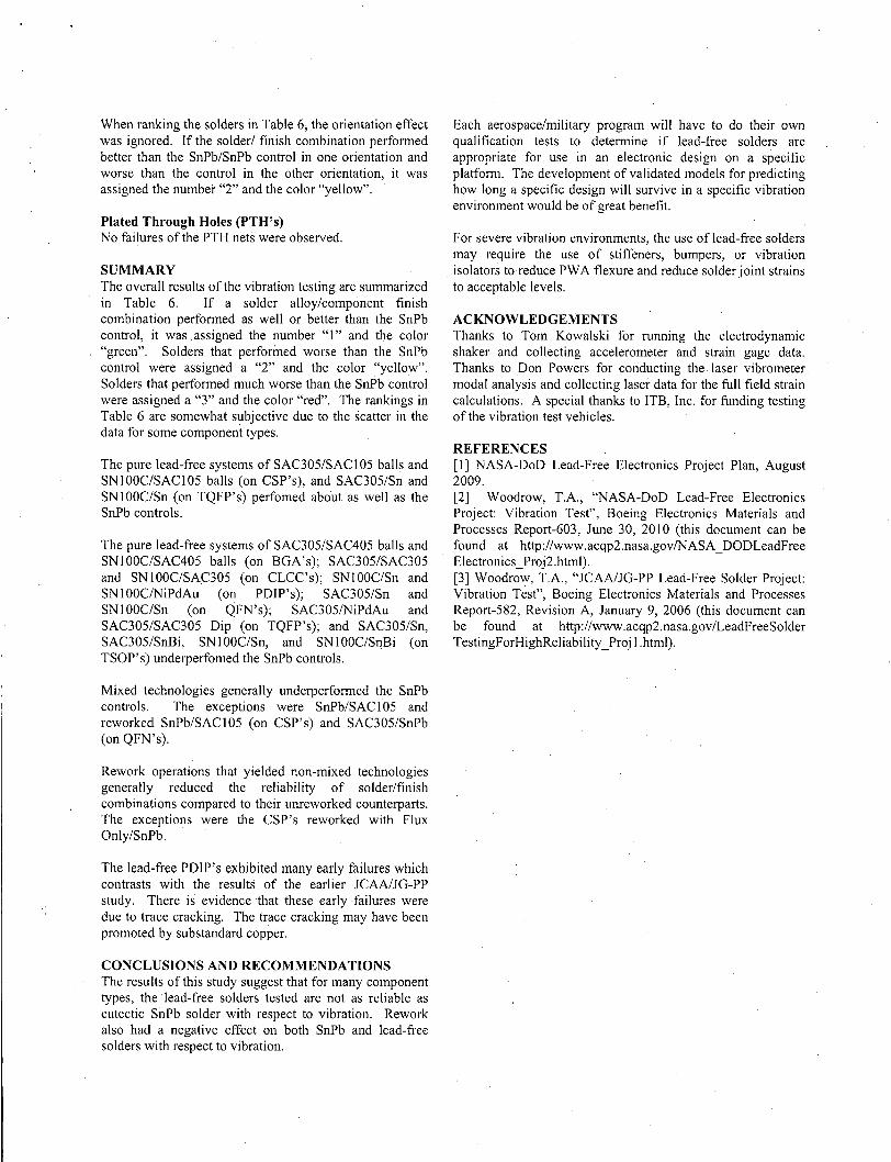
A modal analysis was conducted on the test vehicle located in the end slot of the test fixture using a laser vibrometer system (Polytec Scanning Vibrometer, Waldbronn, Gennany). The end of the fixture was removed during the modal analysis so the vibrometer could scan the test vehicle. The laser vibrometer was used to measure velocities, accelerations, and displacements at 100 points on the bottom surface of Test Vehicle 74 during low level random vibration in the zaxis (the axis perpendicular to the plane of the test vehicle). The laser vibrometer measurements identified 3 major resonance frequencies for the NASA-DoD test vehicle at 65, 390, and 980 Hz. The laser vibrometer data was also used to calculate a bending mode shape for each of the resonances (see examples in Figures 6 and 7).
Most of the "Manufactured" and "Rework" test vehicles were instrumented with two calibrated accelerometers as shown in Figure I for collecting acceleration data during the vibration test. Accelerometer I was located at the
point of maximum deflection for the first and second modes (65 and 91 Hz) and Accelerometer 2 was located at the point of maximum deflection for the seventh mode (390 Hz). The transmissibilites (Q's) for the major modes as measured by each of the accelerometers at each test level were recorded.
Four three-element stacked rosette strain gages were mounted on one test vehicle as shown in Figure.8 to collect strain data in the x and y directions at each test level (directions are defined in Figure I).
Figures 9 through 10 show the transmissibilites and the displacements of a test vehicle vs. frequency (from accelerometer data collected during a I G sine sweep of a "Manufactured" test vehicle in the z-axis). Figure 10 illustrates that the most displacement (and therefore the most solder joint damage) is caused by the first resonance .. The resonance near 390 Hz caused approximately 69 times less displacement than the first resonance at the location of Accelerometer I.
Figure II shows rms strain vs. frequency as measured by two of the strain gages mounted on Test Vehicle 74 (in the xdirection during the 8.0 Grms test). This data demonstrates that the magnitude of the strain is location dependent. Also note that down the centerline of the test vehicle (Strain Gage 4), the strains are produced predominately by the first mode while at the location of Strain Gage 3, the strains produced by the first and seventh modes are nearly equivalent.
The data in Figure II clearly demonstrates that the strain environment at a given location on a test vehicle can be very different from the strain environment at a different location on the same vehicle during the same test. This implies that the best practice is to directly compare identical components in . identical locations on identical test vehicles. It also. implies' that the test solder must be used on one set of test vehicles and the control solder on a second set of test vehicles.
Laser vibrometer velocity data was also collected at 100 points on·the surface of Test Vehicle 74 during a one G sine dwell at the first mode frequency. This data was used to calculate full field peak strains in the vehicle x direction for the first mode (see Figure 12). The calculations were performed using Boeing proprietary software. The regions of calculated maximum strain were down the centerline of the vehicle and along the edges of the vehicle (near the wedgelocks). Note that the strains shown in Figure 12 are compressive down the centerline of the test vehicle and tensile along the edges of the vehicle. When the board bends in the opposite direction the compressive strains will become tensile and the tensile strains will become compressive.
After collection of the modal and strain data, the test vehicles were subjected to a random vibration step stress test in the zaxis only (see Figure I3 and Table 4). The 27 test vehicles were divided into two groups for testing. The first group contained most of the "Manufactured" test vehicles. The

second group contained all of the "Rework" test vehicles and the balance of the "Manufactured" test vehicles.
The test started with one hour of vibration at 8.0 Orms in the z-axis (the axis perpendicular to the plane of the PWA). This was followed by one hour of vibration at 9.9 Orms and then one hour of vibration at 12.0 Orms. The vibration levels were then increased in 2.0 Orms increments, shaking at each level in the z-axis for one hour until completion of the 20~0 Orms run (i.e., a step stress test). The test was completed with one hour of vibration at 28.0 Orms in the z-axis.
Figure 14 shows the shaker input into the test vehicle fixture and Figure 15 shows the typical response of a test vehicle (both during an 8.0 Orms run). Note that the response of the test vehicle differs greatly from the input PSD spectmm with the major test vehicle resonances occurring at 67.5 Hz and 395 Hz.
The 63 components and the PTH mit on each test vehicle were individually monitored using Analysis Tech 256STD Event Detectors (set to a 300 ohm threshold) combined with Labview-based data collection software. The wires connecting the test vehicle to the event detector had to be glued to the surface ofthe test vehicle (Figure I) to prevent them from flexing and breaking during the vibration test.· In addition, the wire bundles from the test vehicle were firmly clamped to the fixture in order to prevent flexing and breaking of the wires. All wire bundles were covered with a grounded metallic shield to prevent electrical noise from the shaker from interfering with the event detectors.
RESULTS AND DISCUSSION Table 5 shows the percent of each component type that failed on both the "Manufactured" and the "Rework" test vehicles at the end of the test. Notice that the QFN-20's were resistant to failure due to vibration.
Figure 16 shows when the components failed on Test Vehicle 74. The failures are colored coded according to which how many test minutes were required to cause the failure (red = 1 to 60 test minutes; orange = 61 to 120 minutes; yellow = 121 to 180 minutes; green = 181 to 240 minutes; blue = 241 to 300 minutes; purple = 30 I to 360 minutes; pink = 361-420 minutes; and white = 421 to 480+ minutes). In general, the components tended to fail first down the centerline and along the edges of the test vehicle (near the wedgelocks). Therefore, the first component failures coincide with the regions of highest strain as shown in Figure 12.
After completion of all vibration testing, the "Manufactured" and "Rework" test vehicles were visually inspected using a HYROX Hi-Scope Compact Micro Vision System (Model KH-2200 MD2). The main goal of the inspection was to document any broken or missing leads on leaded components. This was necessary so that
failures due to solder joint cracking could be distinguished from failures due to lead breakage. The secondary goal of the inspection was to document any unusual failure modes. The complete visual inspection results for each test vehicle can be found in [2]. Some components (BOA's and TSOP's) tended to fall off of the test vehicles during testing. In addition, all wiring was visually inspected to verity that no signal wires had broken during the vibration test (a broken signal wire would look like a solder joint failure to the event detectors). No broken signal wires were found.
Microsections were also done to identity major failure modes. For the BOA's and CSP's, microsections were done on components that failed late in the test in the hope that it would be easier to determine the true failure mechanism since secondary failure mechanisms might not yet have had time to develop.
At the end of the test, numerous components had failed electrically which allowed the relative reliability of the SnPb control solder and the lead-free solders to be compared.
The percentage of each component population that failed was plotted against the accumulated vibration test minutes. Each of the plots groups data from components that were assembled using the same solder alloy/component finish combinations. For example, all of the BOA's in positions U4, U5, and U55 (Figure 17)· used SnPb solder/SnPb balls on the SnPb "Manufactured" test vehicles; SAC 305 solder/SAC405 balls and SNI00C/SAC405 balls on the Pb-Free "Manufactured" test vehicles; SnPb solder/SAC405 balls on the SnPb "Rework" test vehicles; and SAC 305 solder/SnPb balls on the Pb-Free "Rework" test vehicles. The plots in Figure 17 allow a direct comparison between the combined failures of all of these BOA's even though they were in different strain environments during the test.
The overall results of the vibration testing (from the data plots) are summarized in Table 6. If a solder alloy/component finish combination perfornied as well or better than the SnPb control, it was assigned the number" I" and the color "green". Solders that performed worse than the SnPb control were assigned a "2" and the color "yellow". Solders that performed much worse than the SnPb control were assigned a "3" and the color "red".
The rankings in Table 6 are somewhat subjective due to the scatter in the data for some component types. The TSOP data was difficult to interpret since the orientation of the TSOP on the test vehicle appeared to influence how the solder/component finish combinations performed relative to the Sn37Pb/SnPb controls. Weibull plots were not used since the test conditions were changed during the test (i.e., the PSD was increased every 60 minutes) which renders the Wei bull parameters meaningless.
In the following sections, the solder paste used is listed first followed by the component finish (for example,

SAC30S/SAC40S on a BGA is equivalent to SAC30S solderlSAC40S balls).
BGA-22S's The combination of SAC30S solderlSAC40S balls and SN I 00C/SAC405 balls performed poorly when compared to the SnPb/SnPb controls in vibration (see Figures 17, IS, and 19). This is consistent with the results of the earlier JCAAlJG-PP study [3].
Microsections made at the end of the test showed that the comer solder joints failed first. The SnPb/SnPb sections showed solder joint cracking on both the component side and the PWB side of the joints (Figure 20). The SAC305/SAC405 sections showed a number of trace cracks on the component side, PWB trace cracking, and some voiding (see Figures 21 and 22).
The combination of SAC305 solderlSnPb balls and SnPb soiderlSAC405 balls also performed poorly compared to the SnPb/SnPb controls (Figure 17) on either an immersion silver or ENIG board finish. The SnPb/SAC405 BGA's were reflowed using a SnPb reflow profile. The SbPb/SAC405 microsections showed solder joint cracking on the PWB side of the solder joints and trace cracking on the component side (see Figure 23).
SnPb/SnPb BGA's reworked with flux only/SnPb balls and SAC305/SAC405 BGA's reworked with flux only/SAC 405 balls were much less reliable than the SnPb/SnPb control BGA's (Figure IS).
SnPb/SnPb BGA's reworked with SriPb/SAC405 and SAC305/SAC405 BGA's reworked with SnPb/SAC405 also underperformed the SnPb/SnPb controls (Figure 19). The former were reworked with a SnPb thermal profile while the latter were reworked with a Pb-free thermal profile which should have facilitated mixing of the solders.
During rework of the BGA's, problems were encountered with electrical opens. This required that six BGA's be reworked several times instead of just once. See [2] to determine which BGA's were reworked multiple times. In general, the BGA's that were reworked multiple times performed approximately the same as those that were reworked just once.
A few SnPb/SnPb BGA's and SAC305/SnPb BGA's fell off of the test vehicles during the vibration test which allowed the failure mechanisms to be examined more closely. The missing BGA's were on test vehicles with an immersion silver board finish.
On the SnPb/SnPb BGA's that fell off, most of the failures occurred on the package side (Figure 24). Most of the balls were still present (SO.9 to S4.0 percent of the total balls). About half of the missing balls were also missing the associated pads (44.2 to 52.6 percent).
On the SAC30S/SnPb BGA's that fell off, most of the failures also occurred on the package side. Most of the balls were still present (94.7 to 96.9 percent of the total balls). Many of the missing balls were also missing the associated pads (33.3 to 100 percent). Voiding was also observed.
No missing BGA's were seen for the other solder/BGA ball combinations.
CLCC-20's The SnPb/SnPb controls outperformed the combinations of SAC305/SAC305, SNIOOC/SAC305, SnPb/SAC305, and SAC305/SnPb (See Figure 25). .
The amount of Pb detected III the SnPb/SAC305 and SAC305/SnPb solder joints was 24.7% and 16.5%, respectively (from ICP spectroscopy, see Table 3).
Figure 26 shows a crack typical of those found in the CLCC solder joints.
CSP-tOO's The CSP daisy chain pattern on the test vehicles was incorrect with the result that only the outer perimeter balls of each CSP formed an electrically continuous path. In order for aCSP to be detected as failed, both legs of the outer perimeter needed to fail.
The combination of SAC305 solderlSAC I 05 balls and SNIOOC/SACI05 balls generally performed as well as the SnPb/SnPb controls in vibration (see Figures 27 through 29). Microsections made at the end of the test showed that the comer solder joints failed first. Both the SnPb/SnPb and the SAC305/SAC I 05 solder joints fonned cracks on the component side of the CSP's (Figure 30).
The combination of SAC305 solderlSnPb balls slightly underperformed the SnPb/SnPb controls (Figure 27). In contrast, the combination of SnPb solderlSAC I 05 balls outperformed the SnPb/SnPb controls (Figure 27). These SnPb/SAC I 05 components were reflowed using a SnPb reflow profile.
The SnPb/SnPb CSP's reworked with flux only/SnPb balls were about as reliable as the SnPb/SnPbcontrol CSP's while the SAC305/SAC I 05 CSP's reworked with flux only/SAC 105 balls underperformed the SnPb/SnPb control CSP's (Figure 2S).
SnPb/SnPb CS P' s reworked with SnPb/SAC I 05 performed about as well as the SnPb/SnPb controls but the SAC30S/SACI05 CSP's reworked with SnPb/SACIOS greatly underperformed the SnPb/SnPb controls (Figure 29). The former were reworked with a SnPb thennal profile while the latter were reworked with a Pb-free thermal profile which should have allowed complete mixing of the solders.
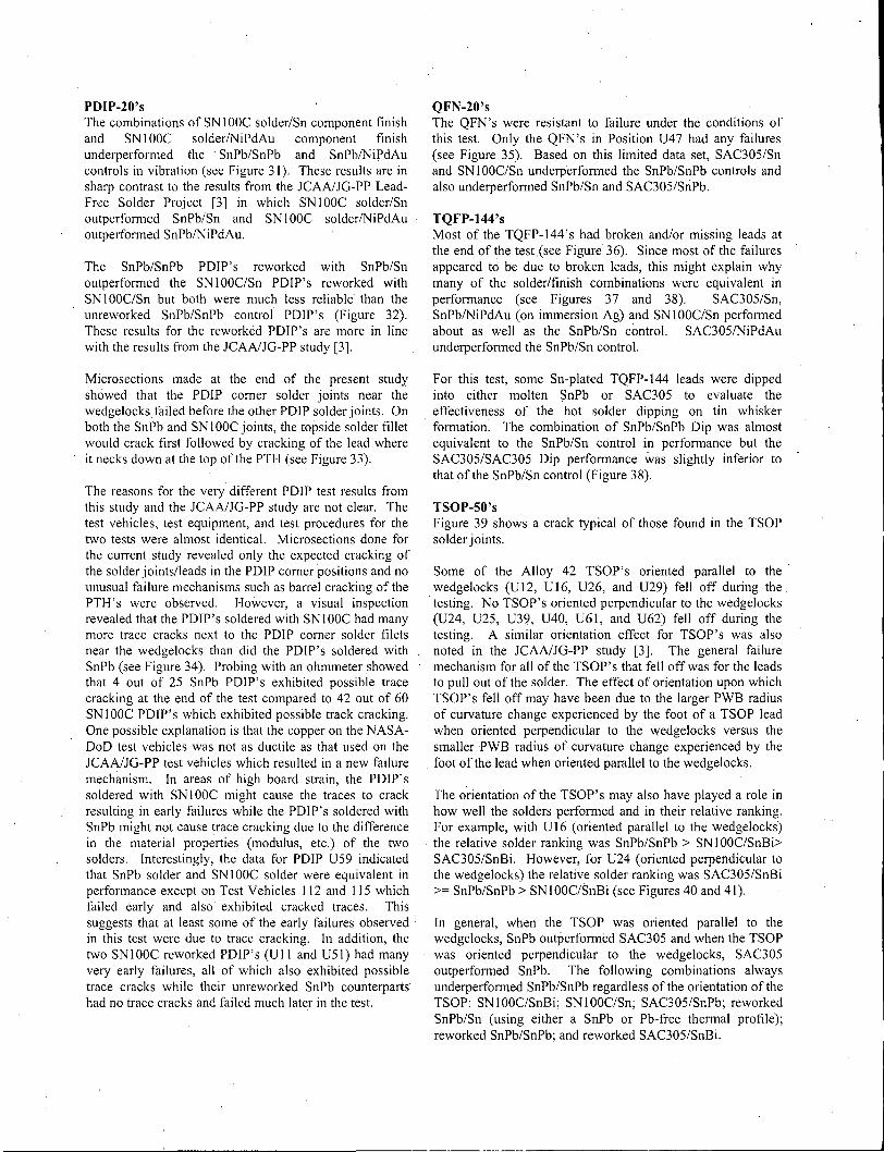
PDIP-20's The combinations of SNIOOC solderlSn component finish and SN I OOC solderlNiPdAu component finish underperfonned the SnPb/SnPb and SnPblNiPdAu controls in vibration (see Figure 31). These results are in sharp contrast to the results from the JCAAlJG-PP LeadFree Solder Project [3] in which SN I OOC solderlSn outperfonned SnPb/Sn and SN I OOC solderlNiPdAu outperfonned SnPblNiPdAu.
The SnPb/SnPb POIP's reworked with SnPb/Sn outperfonned the SNIOOC/Sn POIP's reworked with SN I OOC/Sn but both were much less reliable than the unreworked SnPb/SnPb control POIP's (Figure 32). These results for the reworked POIP's are more in line with the results from the JCAAlJG-PP study [3].
Microsections made at the end of the present study showed that the POIP comer solder joints near the wedgelocksfailed before the other POIP solder joints. On both the SnPb and SNI OOC joints, the topside solder fillet would crack first followed by cracking of the lead where it necks down at the top of the PTH (see Figure 33).
The reasons for the very different POIP test results from this study and the JCAA/JG-PP study are not clear. The test vehicles, test equipment, and test procedures for the two tests were almost identical. Microsections done for the current study revealed only the expected cracking of the solder joints/leads in the POIP comer positions and no unusual failure mechanisms such as barrel cracking of the PTH's were observed. However, a visual inspection revealed that the POIP's soldered with SNIOOC had many more trace cracks next to the POIP comer solder filets near the wedge\ocks than did the PDIP's soldered with SnPb (see Figure 34). Probing with an ohmmeter showed that 4 out of 2S SnPb POIP's exhibited possible trace cracking at the end of the test compared to 42 out of 60 SN I OOC POIP's which exhibited possible track cracking. One possible explanation is that the copper on the NASADoD test vehicles was not as ductile as that used on the JCAAlJG-PP test vehicles which resulted in a new failure mechanism. In areas of high board strain, the POIP's soldered with SNIOOC might cause the traces to crack resulting in early failures while the POIP's soldered with SnPb might not cause trace cracking due to the difference in the material properties (modulus, etc.) of the two solders. Interestingly, the data for POIP US9 indicated that SnPb solder and SNIOOC solder were equivalent in perfonnance except on Test Vehicles 112 and liS which failed early and also exhibited cracked traces. This suggests that at least some of the early failures observed in this test were due to trace cracking. In addition, the two SNIOOC reworked POIP's (UII and U51) had many very early failures, all of which also exhibited possible trace cracks while their unreworked SnPb counterparts had no trace cracks and failed much later in the test.
QFN-20's The QFN's were resistant to failure under the conditions of this test. Only the QFN's in Position U47 had any failures (see Figure 3S). Based on this limited data set, SAC30S/Sn and SNIOOC/Sn underperfonned the SnPb/SnPb controls and also underperfonned SnPb/Sn and SAC305/SnPb.
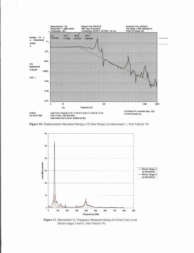
TQFP-144's Most of the TQFP-144's had broken and/or missing leads at the end of the test.(see Figure 36). Since most of the failures appeared to be due to broken leads, this might explain why many of the solder/finish combinations were equivalent in perfonnance (see Figures 37 and 38). SAC305/Sn, SnPblNiPdAu (on immersion Ag) and SNIOOC/Sn perfonned about as well as the SnPb/Sn control. SAC30SINiPdAu underperfonned the SnPb/Sn control.
For this test, some Sn-plated TQFP-144 leads were dipped into either molten $nPb or SAC30S to evaluate the effectiveness of the hot solder dipping on tin whisker fonnation. The combination of SnPb/SnPb Dip was almost equivalent to the SnPb/Sn control in perfonnance but the SAC305/SAC305 Dip perfonnance was slightly inferior to that of the SnPb/Sn control (Figure 38).
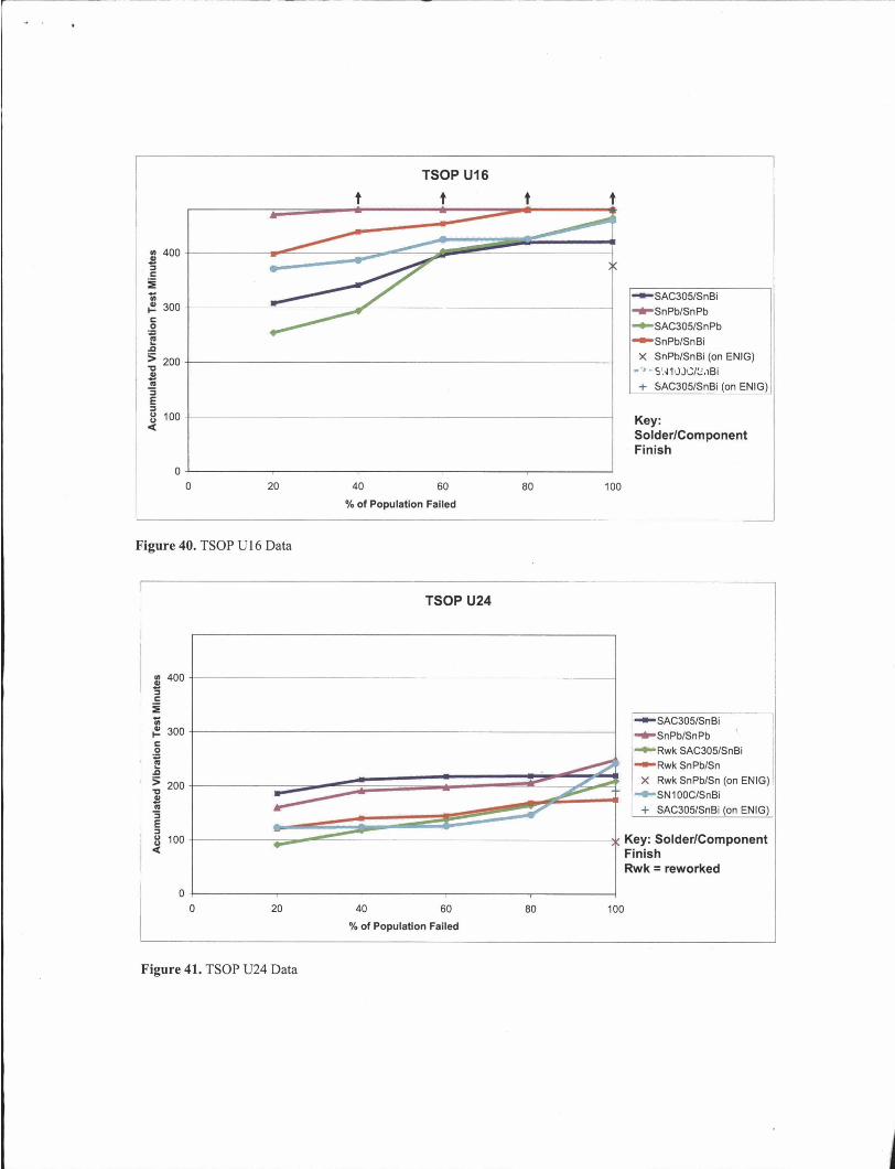
TSOP-50's Figure 39 shows a crack typical of those found in the TSOP solder joints.
Some of the Alloy 42 TSOP's oriented parallel to the wedge\ocks (U 12, U 16, U26, arid U29) fell off during the testing. No TSOP's oriented perpendicular to the wedgelocks (U24, U25, U39, U40, U61, and U62) fell off during the testing. A similar orientation effect for TSOP's was also noted in the JCAA/JG-PP study [3]. The general failure mechanism for all of the TSOP's that fell offwas for the leads to pull out of the solder. The effect of orientation upon which TSOP's fell off may have been due to the larger PWB radius of curvature change experienced by the foot of a TSOP lead when oriented perpendicular to the wedgelocks versus the smaller PWB radius of curvature change experienced by the foot of the lead when oriented parallel to the wedgelocks.
The orientation of the TSOP's may also have played a role in how well the solders perfonned and in their relative ranking. For example, with U16 (oriented parallel to the wedgelocks) the relative solder ranking was SnPb/SnPb > SN I OOC/SnBi> SAC305/SnBi. However, for U24 (oriented perpendicular to the wedgelocks) the relative solder ranking was SAC305/SnBi >= SnPb/SnPb > SNI OOC/SnBi (see Figures 40 and 41).
In general, when the TSOP was oriented parallel to the wedgelocks, SnPb outperfonned SAC305 and when the TSOP was oriented perpendicular to the wedgelocks, SAC305 outperfonned SnPb. The following combinations always underperfonned SnPb/SnPb regardless of the orientation of the TSOP: SN 100C/SnBi; SN 1 OOC/Sn; SAC305/SnPb; reworked SnPb/Sn (using either a SnPb or Pb-free thennal profile); reworked SnPb/SnPb; and reworked SAC305/SnBi.
When ranking the solders in Table 6, the orientation effect was ignored. If the solderl finish combination performed better than the SnPb/SnPb control in one orientation and worse than the control in the other orientation, it was assigned the number "2" and the color "yellow".
Plated Through Holes (PTH's) No failures of the PTH nets were observed.
SUMMARY The overall results of the vibration testing are summarized in Table 6. If a solder alloy/component finish combination performed as well or better than the SnPb control, it was. assigned the number "1" and the color "green". Solders that perforined worse than the SnPb control were assigned a "2" and the color "yellow". Solders that performed much worse than the SnPb control were assigned a "3" and the color "red". The rankings in Table 6 are somewhat subjective due to the scatter in the data for some component types.
The pure lead-free systems of SAC305/SACI05 balls and SNI00C/SACl05 balls (on CSP's), and SAC305/Sn and SNIOOC/Sn (on TQFP's) perfomed about as well as the SnPb controls.
The pure lead-free systems of SAC305/SAC405 balls and SNIOOC/SAC405 balls (on BGA's); SAC305/SAC305 and SNlOOC/SAC305 (on CLCC's); SNIOOC/Sn and SNIOOCINiPdAu (on PDIP's); SAC305/Sn and SNlOOC/Sn (on QFN's); SAC305INiPdAu and SAC305/SAC305 Dip (on TQFP's); and SAC305/Sn, SAC305/SnBi, SNlOOC/Sn, and SNIOOC/SnBi (on TSOP's) underperfomed the SnPb controls.
Mixed technologies generally underperformed the SnPb controls. The exceptions were SnPb/SAC105 and reworked SnPb/SACI05 (on CSP's) and SAC305/SnPb (on QFN's).
Rework operations that yielded non-mixed technologies generally reduced the reliability of solder/finish combinations compared to their unreworked counterparts. The exceptions were the CSP's reworked with Flux Only/SnPb.
The lead-free PDIP's exhibited many early failures which contrasts with the results of the earlier JCAA/JG-PP study. There is evidence that these early failures were due to trace cracking. The trace cracking may have been promoted by substandard copper.
CONCLUSIONS AND RECOMMENDATIONS The results of this study suggest that for many component types, the 'Iead-free solders tested are not as reliable as eutectic SnPb solder with respect to vibration. Rework also had a negative effect on both SnPb and lead-free solders with respect to vibration.
Each aerospace/military program will have to do their own qualification tests to determine if lead-free solders are appropriate for use in an electronic design on a specific platform. The development of validated models for predicting how long a specific design will survive in a specific vibration environment would be of great benefit.
For severe vibration environments, the use of lead-free solders may require the use of stiffeners, bumpers, or vibration isolators toreduce PWA flexure and reduce solder joint strains to acceptable levels.
ACKNOWLEDGEMENTS Thanks to Tom Kowalski for running the electrodynamic shaker and collecting accelerometer and strain gage data. Thanks to Don Powers for conducting the laser vibrometer modal analysis and collecting laser data for the full field strain calculations. A special thanks to ITB, Inc. for funding testing of the vibration test vehicles.
REFERENCES [I] NASA-DoD Lead-Free Electronics Project Plan, August 2009. [2] Woodrow, T.A., "NASA-DoD Lead-Free Electronics Project: Vibration Test", Boeing Electronics Materials and Processes Report-603, June 30, 2010 (this document can be found at http://www.acqp2.nasa.govINASA_DODLeadFree Electronics_Proj2.html). [3] Woodrow, T.A., "JCAA/JG-PP Lead-Free Solder Project: Vibration Test", Boeing Electronics Materials and Processes Report-582, Revision A, January 9, 2006 (this document can be found at http://www.acqp2.nasa.gov/LeadFreeSolder TestingForHighReliability ]roj I.html).

Figurc 1. NASA-DoD Test Vehicle
....... OLI:"~ PC Y5%2 - 1.MO f,... , • .,,g .... _~O_CICOI" 0.. 11.001.01
"OU.CJ')~ATUS .... lI'IIeII'IIIl27C 1IIOtfy .,. -.,. ..... ,,""'" .,.... 00000\0
0... 1Mt'l; 1 TIN .1$ 41 veua
~- ...... --_ ...
..,e •
--' .
C2·tIOOZ"'r
.. LItO_11O
OOOt :p
MaClfl'll .......
,2t
o-oacu 121 c.·OOCl531, ..... 12 ..,
•• 63 Ct.; .. F-=or U ...
• n Cl< r ...
........... ~- ha....,a:.ot\ "''' ....... ''l' ... .,.c
Figurc 2. Reflow Profile for SnPb Solder Paste (Source: BAE Systems)
z

Table 1. Assembly Matrix for "Manufactured" Vibration Test Vehicles
UD8 )23
U49
US9 )30
U38 U, US,
,5 U27 )28
U47
U54
UO,
107
U4,
US8 103
U34
U48
U51
U,2
U2S
U29
,U39 U61
)'6 U24
)26
U40
U6'
Componenl
PC
POI
POIP·20
POIP·20
POlp·20
POII'::20
POlp·20
POlp·20
OFN·2D
OFN·2D
OFN·20
OFN·20
OFN·20
OFP·'44
OFP·'44 ,44
OFP·'44
OFP·'44
OFP·'44
OFP·'44
TOF-"::'44
OFP·'44
OFP·'44
TSD,,·5D
TSOP·SO TSDP·5D
TSOP·SO
TSOP·SO
TSD '·50
TSOP·SO
TSOP·SO
TSOp·50
TSOp·5D
SnPb "Manufactured" Test Vehicles
Test Vehicles 15, 16, 17, 18, 19
SoPb
SoPb
SoPb
SoPb
SoPb
SoPb
SoPb
SoPb
SoPb
SoPb
SoPb
MaHe So
MaHe So
MaHe So
MaHe So
MaHe So
MaHe So
MaHe So
MaHe So
Matte So
Matte So
SoPb
SoPb SoPb
,SoPb
SoPb
SoPb
SoPb
SoPb
SoPb
SoPb
Reflow
Sol, '''oy
SoPb
SoPb
SoPb
SoPb
SoPb
SoPb
SoPb
SoPb
SoPb
SoPb
SoPb
SoPb
SoPb
SoPb
SoPb
SoPb
SoPb
SoPb
SoPb SoPb
SoPb
SoPb
SoPb
SoPb
SoPb
SnPb
SoPb
SoPb
SoPb
SoPb
SoPb
SoPb
SoPb
Pb-Free "Manufactured" Test Vehicles (SAC305 Paste)
Test Vehicles 36, 40, 74, 76, 78, 96 (on ENIG)
See emoce
See 'ereoce :
See Refereoce :
See Refereoce :
See Refereoce :
See Refereoce :
See Refereoce :
See Refereoce :
'So Malle So
Matte So
Matte So
Malle So
Matte So
Malle So
Matte So
Malle So
Malle So
MaHe So
Malle So
MaHe So
MaHe So
MaHe So
So
So
So
So
So
SoBi
S08i
S08i
S08i
SoBi
SAC3DS
SAC3DS
SAC30S
SAC3DS
SAC30S
SAC3DS
SAC30S
SAC30S
SAC30S
SAC3DS
SAC30S
SAC30S SAC3DS
SAC30S
SAC30S
SAC3D'
SAC305
SAC305
SAC305 SAC3D5
SAC305
SAC30S
SAC30S
SAC3DS
SAC305
SN,DDC
SN,OOC
SN,OOC
SN,OOC
SN,OOC
SN,OOC
SN'ODC
SN'DDC
Pb-Free "Manufactured" Test Vehicles (SN100C Paste)
Test Vehicles 111, 112,.113, 114, 115
I Au . NiPdAu
So
So
So
So
So
, MaHeSo
MaHe So
MaHe So
MaHe So
MaHe So
MaHe So
MaHe So
MaHe So
MaHe So
MaHe So
MaHe So
MaHe So
MaHe SI
MaHe So
MaHe So
So
So
So
So
So
SoBi
S08i
S08i
S08i
SoBi
SN,DDC
SN,OOC
SN DOC
SN,OOC
SN,OOC
SN,OOC
SN,DOC
SN,OOC
SN,OOC
SN,DOC
SN,DOC
SN'DOC
~N'DOC SN,
SN,OOC
SN,DDC
SN'OOC SN,OOC
SN,OOC SN,
SN,OOC
SN,OOC
SN,OOC
SN'ODC
SN,ODC
SN,DDC
SN,OOC
SN,OO
SN,
SN,OOC
SN,OOC
SN,
SN,DDC
, l
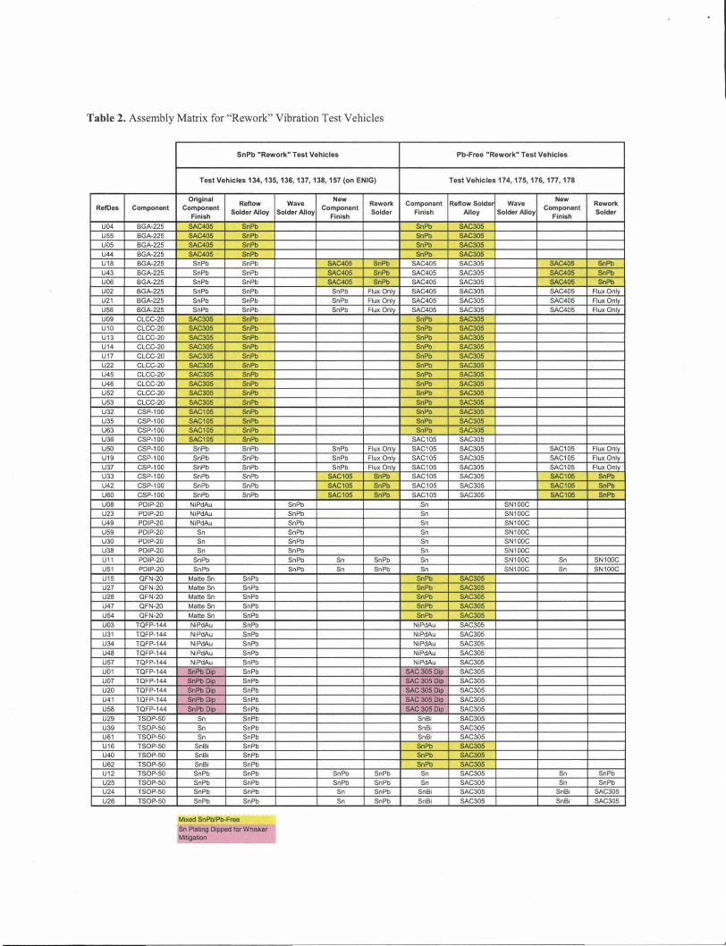
Table 2. Assembly Matrix for "Rework" Vibration Test Vehicles
RofDas Component
U04 BGA-225
U55 BGA-225 U05 BGA-225
U44 BGA-225 U18 BGA-225
U43 BGA-225 U06 BGA-225
U02 BGA-225
U2l BGA-225
U56 BGA-225 U09 CLCC-20 Ul0 CLCC-20
U13 CLCC-20 U14 CLCC-20 U17 CLCC-20
U22 CLCC-20 U4S CLCC-20
U46 CLCC-20 U52 CLCC-20
US3 CLCC-20
U32 esP-l00
U35 esP-l00
U63 CSP-l00 U36 CSP-l00
USO CSP-l00 U19 CSP-l00
U37 CSP-l00 U33 CSP-l00 U42 CSP-l00
U60 esP-l00
U08 PDIP-20
U23 PDIP-20
U49 PDIP-20
US9 PDIP-20
U30 PDIP-20
U38 PDIP-20 Ull PDIP-20
U5l PDIP-20
U15 OFN-20 U27 OFN-20 U28 OFN-20 U47 OFN-20
US4 OFN-20
U03 TOFP-l44
U3l TOFP-l44
U34 TOFP-l44
U48 TOFP-l44
U57 TOFP-l44 UOl TOFP-l44
U07 TOFP-l44
U20 TOFP-144
U41 TOFP-144
U58 TOFP-144
U29 TSOP-50 U39 TSOP-50 U6l TSOP-SO
U16 TSOP-SO U40 TSOP-SO
U62 TSOP-SO U12 TSOP-50 U25 TSOP-SO U24 TSOP-SO
U26 TSOP-SO
SnPb "Rework" Test Vehicles
Test Vehic les 134, 135, 136, 137, 138, 157 (on ENIG)
Original Reflow
Component Soldor Alloy
Finish
SAC405 SnPb
SAC405 SnPb SAC405 SnPb
SAC405 SnPb SnPb SnPb
SnPb SnPb SnPb SnPb SnPb SnPb
SnPb SnPb SnPb SnPb
SAC305 SnPb SAC305 SnPb
SAC305 SnPb SAC30S SnPb
SAC30S SnPb
SAC30S SnPb SAC30S SnPb
SAC305 SnPb SAC30S SnPb
SAC30S SnPb
SAC10S SnPb SAC105 SnPb SAC105 SnPb SAC 1 05 SnPb
SnPb SnPb SnPb SnPb
SnPb SnPb SnPb SnPb SnPb SnPb
SnPb SnPb
NiPdAu
NiPdAu NiPdAu
Sn Sn
Sn
SnPb SnPb
Matte Sn SnPb Matte Sn SnPb Matte Sn SnPb
Matte Sn SnPb
Matte Sn SnPb
NiPdAu SnPb NiPdAu SnPb
NiPdAu SnPb
NiPdAu SnPb
NiPdAu SnPb SnPb DIp SnPb
SnPb Dip SnPb SnPb Dip SnPb
SnPb DIp SnPb
SnPb DIp SnPb
Sn SnPb Sn SnPb Sn SnPb
SnBi SnPb SnBi SnPb
SnBi SnPb SnPb SnPb SnPb SnPb SnPb SnPb
SnPb SnPb
Mixed SnPblPb-Free
Sn Plabng DIpped for Whisker Mitigation
Wave Now
Rework Soidor Alloy
Component Soidor
Finish
SAC405 SnPb
SAC405 SnPb SAC405 SnPb
SnPb Flux Only
SnPb Flux Only
SnPb Flux Only
SnPb Flux Only SnPb Flux Only
SnPb Flux Only SAC10S SnPb SAC10S SnPb
SAC105 SnPb
SnPb SnPb SnPb SnPb SnPb
SnPb
SnPb Sn SnPb SnPb Sn SnPb
SnPb SnPb SnPb SnPb
Sn SnPb
Sn SnPb
Pb-Free "Rework" Test Vehic les
Test Vehicles 174, 175, 176, 177, 178
Component Roflow Soldo Wave Now
Rowork Finish Alloy Soldor Alloy
Component Soldor
Finish
SnPb SAC305
SnPb SAC305 SnPb SAC305 SnPb SAC305
SAC405 SAC305 SAC405 SnPb
SAC405 SAC305 SAC405 SnPb SAC405 SAC305 SAC405 SnPb SAC405 SAC305 SAC405 Flux Only
SAC405 SAC305 SAC405 Flux Only
SAC405 SAC305 SAC405 Flux Only
SnPb SAC305 SnPb SAC305
SnPb SAC305 SnPb SAC30S SnPb SAC305
SnPb SAC30S SnPb SAC30S
SnPb SAC305 SnPb SAC305
SnPb SAC30S
SnPb SAC30S SnPb SAC305 SnPb SAC305
SAC10S SAC30S
SAC10S SAC30S SAC10S Flux Only
SAC105 SAC305 SAC10S Flux Only
SAC105 SAC305 SAC10S Flux Only
SAC 1 05 SAC30S SAC105 SnPb
SAC 1 05 SAC305 SAC10S SnPb
SAC 1 05 SAC305 SAC105 SnPb
Sn SN100C
Sn SN100C
Sn SN100C
Sn SN100C Sn SN100c
Sn SN100C
Sn SN100C Sn SN100C
Sn SN100C Sn SN100C
SnPb SAC30S SnPb SAC305 SnPb SAC305
SnPb SAC305
SnPb SAC305
NiPdAu SAC30S
NiPdAu SAC30S
NiPdAu SAC305
NiPdAu SAC30S
NiPdAu SAC30S SAC 305 Dip SAC30S SAC 305 DIp SAC30S
SAC 305 DIp SAC305
SAC 305 DIp SAC30S
SAC 305 Dip SAC305
SnBi SAC305 SnBi SAC305 SnBi SAC305
SnPb SAC305 SnPb SAC305
SnPb SAC305 Sn SAC30S Sn SnPb
Sn SAC305 Sn SnPb SnBi SAC30S SnBi SAC305
SnBi SAC30S SnBi SAC305

"OI..l..,rrA'TUI .... w..nMT tIC _._'*' AIrItIIr 12:301M ........ 000\ 4
-""' ... T ... Dal;:I WI ..
""----.. 4 ""--
Ct-OO:014,J,
' .. ... 10' ''0
,. .. ,.
a-O)0341 , 20 • , .. .. , ' .. 1M
, .. 00<1104, QO"OI(2, CO,","
- ... -'.11 '" t'U '" '5> I), ' ... '12 .... ... .",. U.
Figure 3. Reflow Profile for SAC305 and SNIOOC Solder Pastes (Source: BAE Systems)
...... ..,c ..,c ..,c ..,c ..,c dooC
Table 3. Chemical Analysis of Solder Joints Contaminated with Pb (by rcp Spectroscopy)
Component Ref, Des. Test
Reworked? Component Finish Board
Solder 'IoAg %Cu 'IoPb Vehicle 10 Finish
BGA-225 U04 149 No SAC405 AQ Sn37Pb 3.46 0.94 3.77 BGA-225 U04 193 No Sn37Pb Aa SAC305 0.31 0.26 33.91
BGA-225 U43 193 Ves SAC405 Residual
Sn37Pb 3.13 3.18" 5.52 SAC
CLCG-20 U09 149 No SAC305 AQ Sn37Pb 1.35 0.49 24.68 CLCG-20 U09 193 No Sn37Pb Ag SAC305 1.92 0.39 16.46
CSP-100' U33 149 Ves SAC105 Residual
Sn37Pb 0.90 0.73 1.81 Sn37Pb
CSP-100' U33 193 Ves SAC105 Residual
Sn37Pb 0.83 0.63 4.43 SAC
QFN-20 U15 193 No SnPb A9 SAC305 3.39 0.85 0.93
TSOP-50 U16 149 No SnBi Aa Sn37Pb 0.44 2.68" 35.73 TSOP-50 U16 193 No SnPb Aa SAC305 3.53 6.10" 1.51
'PWB Cu pads had to be cut from the CSP balls. This oparation also removed thai end of each ball . ... Copper may have been removed from the PWB pads when the solder joints were cut from the test vehicle.
%Sn %81 'IoAu
91 .71 0.00 0.13 65.44 0.00 0.08
88.07 0.00 0.10
73.48 0.00 0.00 81 .19 0.04 0.00
96.23 0.00 0.33
93.82 0.00 0.29
94.83 0.00 0.00
61 .06 0.09 0.00 88.86 0.00 0.00

Figure 4. Test Vehicles in Fixture
Figure 5. Test Vehicles in Fixture Mounted on the Electrodynamic Shaker

Figure 6. Mode Shape at 65 Hz
Domain FFT
Signal Vib ~ Ref1 FRFVeJocity ... S~ Inst. Value
U
1 e-3 m/s I mJsZ
""'~ ·5 5
Zoom 197%
r -------------, ',.' I . , , , , , , , , , I ______ J
Figure 7. Mode Shape at 390 Hz

Figure 8. Strain Gage Placement on Test Vehicle 74
• Hz 102. AI8bt CII 5 VI~ 43153 USl3 20512
ftntnIobI
IItftBnct
10
lCl!l
ACI': 1
001 ~ __________________________________________ ~
5 100
1..eaHf~,141loirds.74,15.1 1111116.112,40 11,113 76,18.11ua RlllflZ~ lGjlkSileSc:an ,
TI!!lNalm:III2167 ~.OOI
2IlOO
Figure 9. Transmissibilities at Each Major Resonant Frequency Measured During a 1G Sine Sweep (Accelerometer 1, Test Vehicle 74)
·Auxby CIl 5 A FlIldamertal
Callrd A
Log llsplaoement
In(pki*)
ACP: 1
o
- ------- -- - -------- ---- - ----- ----------
Sweep Nl.mber: 1.00 Sweep Rate 1: 1.0000 oct/lrjn
: 60%
1 2 7021 90.48 0.17398 0.015180
8apsed llme: 000:08:38 Rler Type: PropOlllonal Fundamental: 20.000 %, BB RMS: 1.59
3 3f11.9
Remaining llme: 000:00:01 Test R~e: 5.000, 2000.000 Hz Ports Per SW 450
1~_t-~----------------~----r_~------------~--~----~~~r_------~ $
13:32:21 Tue ~I 07 2009
10
Log Frequency (Hz)
100
Lead-Free,14 Boards:74,15,lll,38,16,l12AO,17,l13,76,18,l14,78 Run'l Z-axis, lGpk sne Scan , [)ala Re'llew Rle A: 1112167 leadfree..yfb.004
1000
A:5Z Board 174, connector edge [Up] A: Control [Sweep Up]
2000
Figure 10. Displacements Measured During a IG Sine Sweep (Accelerometer 1, Test Vehicle 74)
c 'e OJ ~ u :i III
E
60
50
40
30
20
10
~~I I
a 100 200 300 400 500 600 700 800 900
Frequency (Hz)
Figure 11. Microstrain vs. Frequency Measured during 8.0 Grms Test Level (Strain Gages 3 and 4, Test Vehicle 74)
- Strain Gage 3 (x-direction)
- Strain Gage 4 (x-direction)

o en Q.
0,01
0,001
: ........ ..
1IlO
;.,
100
..... ; .. ' .'
· 100
·200
·2
Y (inches)
X (inches)
Figure 12. Full Field Peak Strains at 65 Hz (lG Sine Dwell, Test Vehicle 74)
f i
/~
I ~ ~ I . ' I I I
I I . I I I I I I I 'If ) 1 r// J / / V/ ) '1 I I
V'l I ,
10 100
Frequency (Hz) Figure 13. Vibration PSD 's for Step Stress Test
"-
'" \. ~\
" " "- "- "-"-"- "-"-
'\. '\. '\. ' \. \.' \
1000
. '~. ~. ,
.~ ..
L .•
"'" ~' .
-Level 1
- Level 2
- Level 3
- Level 4
- LevelS
- Level 6
- Level 7
- LevelS
10000

,----- ------------ --------
Table 4. Vibration Test Levels
Level 1 Level 2
20 Hz @ 0.00698 G2/Hz 20 Hz @ 0.0107 G2/Hz 20 - 50 Hz @ +6.0 dB/octave 20 - 50 Hz @ +6.0 dB/octave
50 - 1000 Hz@ 0.0438 G2/Hz 50 - 1000 Hz @ 0.067 G2/Hz
1000 - 2000 Hz @ -6.0 dB/octave 1000 - 2000 Hz @ -6.0 dB/octave
2000 Hz @ 0.0109 G2/Hz 2000 Hz @ 0.0167 G2/Hz Composite = S.O Grms Composite = 9.9 Grms
Level 4 LevelS
20 Hz @ 0.0214 G2/Hz 20 Hz @ 0.0279 G2/Hz 20 - 50 Hz@ +6.0 dB/octave 20 - 50 Hz @ +6.0 dB/octave
50 - 1000 Hz @ 0.134 G2/Hz 50 - 1000 Hz @ 0.175 G2/Hz
1000 - 2000 Hz @ -6.0 dB/octave 1000 - 2000 Hz@ -6.0 dB/octave
2000 Hz @ 0.0334 G2/Hz 2000 Hz @ 0.0436 G2/Hz Composite = 14.0 Grms Composite = 1S.0 Grms
Level 7 LevelS
20 Hz @ 0.0437 G2/Hz 20 Hz @ 0.0855 G2/Hz 20 - 50 Hz @ +6.0 dB/octave 20 - 50 Hz @ +6.0 dB/octave
50 - 1000 Hz @ 0.2734 G2/Hz 50 - 1000 Hz @ 0.5360 G2/Hz
1000 - 2000 Hz @ -6.0 dB/octave 1000 - 2000 Hz @ -6.0 dB/octave
2000 Hz @ 0.0682 G2/Hz 2000 Hz@ 0.1330 G2/Hz Composite = 20.0 GrIM Composite - 2S.0 Grms
100 !
10 ! :
[l.ag] t ~. I
fill 1lOf2DO '1 : 1 i
AIlS: &.11039
:
0.1 y
.L.
0.01 Z
Aa': 1
0.001 :
~ .. -!
O.DOO1 ,
100
I.eed RH,loIbaatds.14, 15, 111,36,1&'112:40,17,11"18, 11-4,78, 19 Rill fl. Z.u.1IIldcn. a.oam., Test NaiTe: tn2167 LtIllH1lt 8Gnr&00I
Figure 14. 8.0 Grms Input (Z-axis)
Level 3
20 Hz@ 0.0157 G2/Hz 20 - 50 Hz @ +6.0 dB/octave 50 - 1000 Hz @ 0.0984 G2/Hz
1000 - 2000 Hz @ -6.0 dB/octave
2000 Hz @ 0.0245 G2/Hz Composite = 12.0 Grms
LevelS
20 Hz @ 0.0354 G2/Hz 20 - 50 Hz @ +6.0 dB/octave
50 - 1000 Hz @ 0.2215 G2/Hz
1000 - 2000 Hz@ -6.0 dB/octave
2000 [email protected] G2/Hz Composite = 1S.0 Grms
Till Range: 2DJXlO, • .GOOHz ~: 2.SXIHz
.. -.
.
..
~ -.~
1000

AuXiliary . 5
Reference
[Los]
s'IHz OOF 120 RMS: 34.707.g 8.011 S
09:5Z:ze OIhJul-Z009
20
[Los]
Releren"" RMS: 8.011 CI~InS: 3.00 Slsma
100
Frequency (Hz)
Lead Free, l.o1boards:74.1S.11 1.36.16.112.40.17.113.76.16.' ...... 78.19 RIJtl 12. Z-alds mndom. B.DOrms,
Test Name: 1n2167_lead-Fme.e.Grms.cxn
T.., Rang.: 20.000. 2000.000 Hz Resc1utlon: 2.500 Hz
1000
5z Board 114. ccnneclCr odse
2000
Figure 15. Test Vehicle Response (8.0 Gnns, Z-axis, Accelerometer I, Test Vehicle 74)
Table 5. % of Components Failed (Includes Mixed Solders)
% of Components Failed During Vibration Testing
"Manufactured" Test Vehicles "Rework" Test
Vehicles SnPb SAC305 SN100C SnPb Pb-Free Paste Paste Paste Paste Paste
Component
BGA-225 84 98 100 100 100 CLCC-20 32 43 90 35 68 CSP-100 62 .73 70 62 80 PDIP-20 98 92 100 88 96 QFN-20 0 21 20 8 10
TQFP-144 60 63 64 70 70 TSOP-50 62 73 86 77 80

Figure 16. Test Minutes Required for Components to Fail (Test Vehicle 74 Data)
BGAs U4, U5, U55
VI 400 GI
"5 e: :i -VI GI 300 l-e: .2 ~ .. .c :> 200 "0 GI ~ "5 E :::l U 100 -u <
o 20 40 60 80
% of Population Failed
Figure 17. Combined Data from BGA's U4, U5, and U55
100
-SAC305/SAC405 "'-SnPb/SnPb .... SAC305/SnPb
- SnPb/SAC405 (SnPb Profile) X SnPb/SAC405 (on ENIG)
..... SN100C/SAC405
+ SAC305/SAC405 (on ENIG)
Key: Solder/Component Finish

BGAs U2, U21, U56
t t t t
VI 400 -$ ~ I:
~ Vi GI 300 l-I: .2 1;; .. J:l
:> 200 "0 GI 1;; "5 E ~ u 100 u «
o +---------------.---------------------~ o 20 40 60 80 100
% of Population Failed
- SAC30S/SAC40S ..... SnPb/SnPb
~Rwk Flux Only/SAC40S
- Rwk Flux Only/SnPb
X Rwk Flux Only/SnPb (on ENIG)
... SN 1 00C/SAC40S
+ SAC30S/SAC40S (on ENIG)
Key: Solder/Component Finish Rwk = reworked
Figure 18. Combined Data from BGA's U2, U21 , and U56
~ 400 '5 I: :§ -VI GI 300 l-I:
:8 til ..
J:l :> 200 "0 $ til "5 E ~ u 100 u «
0
BGAs U6, U18, U43
t t t t
-SAC30S/SAC40S
-"SnPb/SnPb
~Rwk SnPb/SAC40S (Pb-Free Profile)
- Rwk SnPb/SAC40S (SnPb Profile)
X Rwk SnPb/SAC40S (on ENIG)
I~SN 1 00C/SAC40S
I + SAC30S/SAC40S (on ENIG)
1 --I!~~~---'~-,-------.....,..------__r------_1 Key: Solder/Component Finish + Rwk = reworked 0 20 40 60 80 100
% of Population Failed
Figure 19. Combined Data from BGA 's U6, Ul 8, and U43

------------------ -------------- ------------
Figure 20. Test Vehicle 15 - Corner Ball ofBGA U21 (SnPb SolderlSnPb Balls)
Figure 21. Test Vehicle 36 - Corner Ball ofBGA U21 (SAC305 SolderlSAC405 Balls)

Figure 22. Test Vehicle 36 - Trace Crack on Component Side of BGA U21 (SAC305 SoiderlSAC405 Balls)
Figure 23. Test Vehicle 134 - Comer Ball ofBGA U44 (SnPb SoiderlSAC405 Balls)

Figure 24. Test Vehicle 16 BGA US (SnPb SolderlSnPb Balls)
CLCCs U13, U14
VI 400 CII -:I s::::
~ -VI CII 300 l-s:::: 0 ;: ns ...
.Q
:> 200 "C CII -..!.'!! :I E :I U 100 u «
O+-------,-------,-------,-------,-----~
o 20 40 60 80 100
% of Population Failed
Figure 25. Combined Data from CLCC's Ul3 and U14
-SAC305/SAC305 ..... SnPb/SnPb ~SAC305/SnPb
- SnPb/SAC305 X SnPb/SAC305 (on ENIG)
..... SN 1 00C/SAC305
+ SAC305/SAC305 (on ENIG)
Key: Solder/Component Finish

Figure 26. Test Vehicle 78 CLCC Ul4 (Cracked SAC30S/SAC30S Solder Joint)
CSPs U35, U63
t t
o 400 ~--------------~ __ --~~~~~~~~~--~~~~~~~ ~ " :iii
~ I _--~::==~~~~s:~::~~~;:~~~~~~------------~ ~ 300 t " o
~ J:J
> 200+-----~~----------------------------------------------~ " .!l co "3 E ::I ~ 100 +--------------------------------«
O+----------,----------~----------~----------~--------~ o 20 40 60 80 100
% of Population Failed
Figure 27. Combined Data from CSP U3S, U63 Data
-SAC305/SAC105 ..... SnPb/SnPb .... SAC305/SnPb - SnPb/SAC105 (SnPb Profile) .... SN100C/SAC105
X SnPb/SAC105 (on ENIG) + SAC305/SAC105 (on ENIG)
Key: Solder/Component Finish

% of Population Failed
Figure 28. Combined Data from CSP's UI 9 and USO
CSPs U33, U42
t
~ 400 --r-----------------------------~~~~~~~~--~~~_1 :; I:
i
~ 30ot---~==~~~~~~:::;~;:~:.~--~~~~~I1~~--_i a ~ .Q
~ 200 +---------------------------------------~------------_4 ~ :; E
" ~ 100 t---~~----------------------------------------------~
<
O+---------~--------~--------~~--------~------~ o 20 40 60 80 100
% of Population Failed
Figure 29. Combined Data from CSP's U33 and U42
- SAC305/SAC105 ..... SnPb/SnPb ~Rwk SnPb/SAC105 (Pb-Free Profile) - Rwk Sn Pb/SAC 1 05 (SnPb Profile)
X Rwk SnPb/SAC105 (on ENIG) ~SN100C/SAC105
+ SAC305/SAC105 (on ENIG)
Key: Solder/Component Finish Rwk = reworked

Figure 30. Test Vehicle 36 - Comer Ball ofCSP U35 (SAC305 SoideriSAC105 Balls)
1l 400 ::I C
~ iii ~ 300 c o ., I'!! .a :> 200 "t:I
~ "3 E ::I CJ 100 ~
o o
~
'7 20
PDIPs US, U49
~ 40 60
% of Population Failed
Figure 31. Combined Data from PDIP's U8 and U49
--2 .-
~
80 100
-SN100C/Sn ...... SnPb/SnPb - SnPb/NiPdAu ~ SN1 OOC/NiPdAu
X SnPb/NiPdAu (on ENIG) + SN100C/Sn (on ENIG)
Key:Solder/Component Finish

PDIPs U11, U51
S 400 +-----------------------------------------------------~ ::I C
:i OJ ~ 300 +-----------------------------------------------~~~~ c ~ t!!
.Q
~ 200 t-------------~~----.. ----~------------------------_; .! .. '5 E ::I U 100 +-------------------------~r_------------------------~ ~
o 10 20 30 40 50 60 70 80 90 100 % of Population Failed
Figure 32. Combined Data from PDIP's UII and USI
~SnPb/SnPb
- SN100C/Sn ""-Rwk SN100C/Sn - Rwk SnPb/Sn
X Rwk SnPb/Sn (on ENIG)
Key: Solder/Component Finish Rwk = reworked
Figure 33. Test Vehicle 175 - Comer Lead ofPDIP US1 (Reworked SNIOOC Solder/Sn Finish)

Figure 34. Test Vehicle 112 - Cracked Trace at Comer ofPDIP U38 (SNlOOC/Sn)
QFN U47
t t t t t
til 400 41 -::J s::::
:E -til 41 300 l-s:::: 0
:;:; CQ .... .c :> 200 'C 41 -CQ
~ E ::J U 100 u <{
O +--------r----------------,--------.------~
o 20 40 60 80 100
% of Population Failed
Figure 35. Data from QFN U47
-SAC30S/Sn -*-SnPb/SnPb ..... SAC30S/SnPb - SnPb/Sn - SN100C/Sn + SAC30S/Sn (on ENIG)
Key: Solder/Component Finish

g: 400 -::I C
:i u; GI 300 ~ c .2 1V ... .c ::; 200 "0 oS CIS '3 E ::I U 100 u «
0
0
Figure 36. Test Vehicle 16 - Cracked Leads and Missing Lead on TQFP U58 (SnPb/Sn)
TQFPs U3, U57
-SAC305/Sn ..... SnPb/Sn
~SAC305/NiPdAu
- SnPb/NiPdAu X SnPb/NiPdAu (on ENIG)
.... SN100C/Sn + SAC305/Sn (on ENIG)
Key: Solder/Component Finish
20 40 60 80 100
% of Population Failed
Figure 37. Combined Data from TQFP's U3 and U57
III Q) -::I c:: ~ -III Q)
~ c:: 0 ;:: CG ... .c :> " Q) -CG :i E ::I U u ~
TQFPs U20, US8
400
300
200
100 X
O +-------~------~------~------~----~
o 20 40 60 80 100
% of Population Failed
-SAC305/Sn -a-SnPb/Sn ...... SAC305/SAC305 Dip
- SnPb/SnPb Dip
X SnPb/SnPb Dip (on ENIG)
- SN100C/Sn
Key: Solder/Component Finish
Figure 38. Combined Data from TQFP's U20 and U58
Figure 39. Test Vehicle 36 - Cracked Solder Joint on TSOP U25 (SAC305/Sn)
TSOP U16
t t
,; 400 :::I I:
i 0 <Il 300 .... I: 0
~ ,g
:> 'tl
200 ~ co "5 E :::I U 100 u cI:
0
0 20 40 60
% of Population Failed
Figure 40. TSOP U16 Data
TSOP U24
III 400 ~ :::I I:
i 0 <Il 300 .... I:
~ f! .Q --:> 200 'tl
~ '3 E :::I ..-(J 100 (J
cI:
0
o 20 40 60
% of Population Failed
Figure 41. TSOP U24 Data
t t
80 100
~ ~ -' ~
:...r
80 100
------------
-SAC305/SnBi
-&-SnPb/SnPb ~SAC305/SnPb
- SnPb/SnBi
X SnPb/SnBi (on ENIG) • ' •• S ', 41 IJjI':;/~,lBi
+ SAC305/SnBi (on ENIG)
Key: Solder/Component Finish
- SAC305/SnBi -&-SnPb/SnPb
~Rwk SAC305/SnBi - Rwk SnPb/Sn
X Rwk SnPb/Sn (on ENIG) ..... SN100C/SnBi
+ SAC305/SnBi (on ENIG)
Key: Solder/Component Finish Rwk = reworked

Table 6, Ranking of Solder Alloy/Component Finish Combinations
Com nent QFN-20
Com nent TQFP·144
Sn37PblSn37Pb 1
Sn37PblSn SAClO5lSn
Key: SolderIComponent Finish Rwk = rewo,*ed
1
·Perfonnance relattve to Sn37Pb control may depend on orientation of the TSOP
Sn37Pb/SACl05
Sn37Pb/SAC105
Sn37Pb/Sn 1
Sn37PblNIPdAu SAC30SINIPdAu 2
Sn37PblSnBI SAC305lSn
2- 2-
1 = as good as or better than Sn37Pb control 2 = worse than Sn37Pb control 3 = much worse than Sn37Pb control
Rwk Flux Only/SAC.fOS SN100ClSAC405
Rwk Flux OntylSAC1D5 SN100C/SAC105
SN100ClSn 2
Sn37PblSn37Pb 0 1 SAC305lSAC305 01 SN100ClSn 2 1
SAC30SlSnBI SAC305lSnPb Rwk Sn37PblSnPb Rwk SAC305lSnBI
2'
!
.~