Nanotechnology Approaches to Sensing and Detection
19
Nanotechnology Approaches to Sensing and Detection Dr. James S. Murday Dr. Richard J. Colton Naval Research Laboratory Washington, DC 20375-5342 [email protected]
Transcript of Nanotechnology Approaches to Sensing and Detection

Nanotechnology Approaches to Sensing and Detection
Dr. James S. MurdayDr. Richard J. ColtonNaval Research Laboratory
Washington, DC [email protected]

Why Nanostructures for Sensing
•Signal to noise improvements:
yocto(10-24)joule,
atto(10-18)newton,
single molecule, ….
• Miniaturization – size/weight - arrays
• Lower power, potentially scavenged
• Locally process data into information
Nanocalorimeter; Roukes CIT
Cantilever Sensor; Thundat ORNL
Molecular Motor; Montemagno Cornell
Lab-on-a-chip; Sandia
+
15 µ NanoAu Chemiresistor; Snow NRL
M agneticbead
DN A-coatedpad
Fie ldgeneration w ire
Shortingm etal
M agneto res is tivestrip
GMR Biosensor; Whitman/Prinz, NRL
Murday, NRL #133 11/01

Nanotechnology Approaches to Sensing & Detection
Outline• Approaches
– Electron tunneling transducers (STM inspired)– Micromechanical detection (AFM inspired)– Nanowire/tube– Nanoparticle
• Power sources• Looking ahead
Micromechanical Approaches – AFM inspiredThundat ORNL Protiveris – VeriScan 3000
Lang IBM Zurich Concentris – Cantisens
Veeco - Scentris
Bashir Purdue
Craighead Cornell
Fadel Univ Bordeaux
Majumdar UCB
Whitman NRL
Ziegler Univ Kaiserslautern
Cantilever Sensor Array Bibliography - http://www.veeco.com/pdf/CSA_Bibliography.pdf

Micromechanical Sensing & Detection
H.P. Lang, et al., Anal. Chim. Acta 393, 59 (1999)
Micromechanical cantilevers
temperature~10 µK res
calorimeter(fJ)
chemical rxn
photothermal
environmentalsensor
surface stress
AFMchargesensor
microbalance(pg)
mag. field
flowsensor

Cantilever Array-based Artificial Nose
M.K. Baller, et al., Ultramicroscopy 82, 1 (2000); F.M. Battiston, et al., Sensors & Actuators 77, 122 (2001)
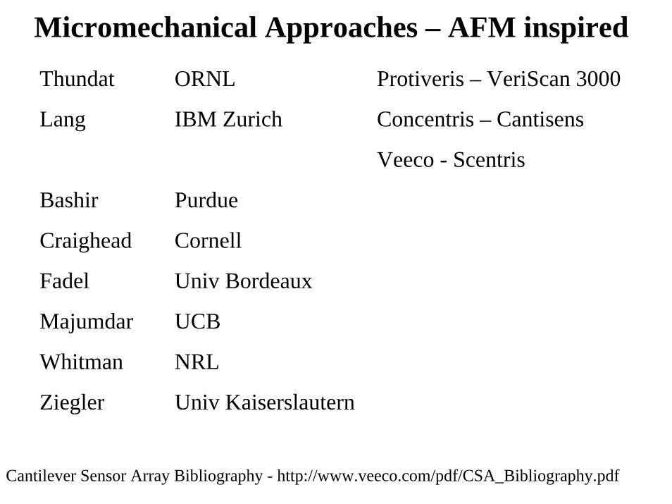
Force Amplified Biological Sensor
Cantilever
Analyte
Antibody-coatedmagnetic bead
Magnetic field exertsforce on bead
Electromagnetcoils
Cantilever
Analyte
Antibody-coatedmagnetic bead
Magnetic field exertsforce on bead
Electromagnetcoils 4-Layer Flexible Circuit
and Aluminum Enclosure
1 of 24-cantilever dies
Before magnetic field After magnetic field Before magnetic field After magnetic field FABS Assay for Ovalbumin at 1 ng/mL
D.R. Baselt, et al. JVST B 14, 789 (1996); Proc. IEEE 85, 672 (1997)

Nanowire/Nanotube Approaches
Dai StanfordDekker Delft (ND)Grimes Penn StateLieber HarvardSnow NRLValentini Univ Perugia (IT)

Chemical sensing with C nanotube networksE.S. Snow and F.K. Perkins
Graphic/Concept
C nanotube network sensor element
•Sensor based on capacitance of SWNT network•Detection via field-induced polarization of adsorbates on SWNT surface•Fast, low-power, and highly sensitive•Responds to CWAs, TICs and explosives•Chemical specificity achieved using chemically selective coatings•Functionalized arrays for detection and identification
50 100 150 200 250 300 350 400Time (s)
0
2
4
6
8
10
12
14
16
18
20
∆C/C
x10
3
0.012 %
0.003 %
P/P0 = 0.03 % Acetone

III. Biosurfaces on III-V Substrates for bioFETs
III. Biosurfaces on III-V Substrates for bioFETs
An ideal surface chemistry would:
1. Preserve the electronic integrity of the underlying substrate while remaining thin enough for efficient sensing (~2 nm).
source drain
GATE REGION
electrode adsorbatesor
source drainsource drain
GATE REGION
electrode adsorbatesor
FET
VersatilityVersatility
2. Allow for specific attachment of DNA or protein molecules.
3. Resist the nonspecific adsorption of other biological materials (lower background & false positives).
For many substrates (e.g. InAs, GaN), no such chemistry currently exists.

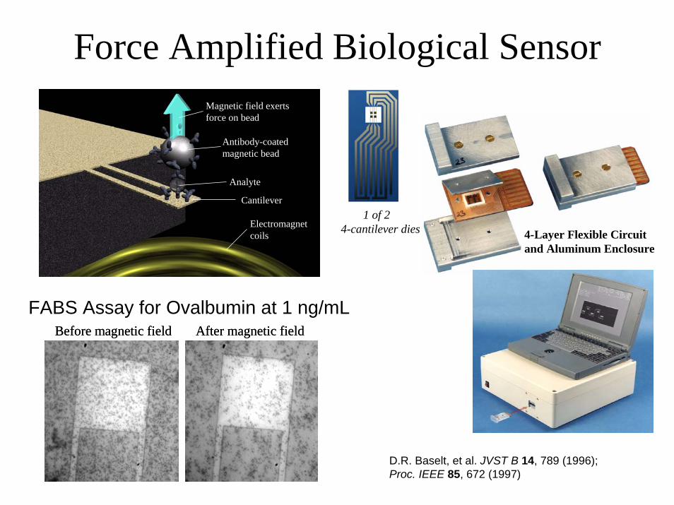
(Nano)particle Approaches
Alivasatos UCB Quantum Dot Corp – QDot BioconjugatesMirkin Northwestern Nanosphere, Inc - VerigeneSnow NRL Microsensor Systems, IncWhitman NRL Seahawk BiosystemsLu Univ IllTan FloridaTan Nanyang Tech Univ (PRC)
• Prepare QDs conjugated with anti-RDX antibodies• Measure PL of QD-bioconjugates bound to a surface prepared with RDX analogs• Free RDX competes for bioconjugate and reduces PL signal
Substrate
ImmobilizedRDX analog
Anti-RDXantibody
FreeRDX
Luminescent QD
RDX concentration (ng/ml)0.1 1 10 100 1000
PL s
igna
l (a.
u.)
Sensitivity to 5 nM RDX
Competition Assay
Detection of Explosives (RDX) in Seawater
Also in solid & water environmental samplesE.R. Goldman, et al., Environ. Sci. Technol. 37, 4733 (2003)
E.R. Goldman, et al., Anal. Chim. Acta 457, 13 (2002)
NRL, Code 6900

DC VOLTAGE
Chemiresistor Dev iceM icron Scale Coated Elect rode
Indiv idual Nanoclust ers
A MM ETER
Sorpt ion of V apor
ssssss ss ssss
sss
ssss ssssssss ss ssss
sss
sssss
ssssssss ssss
sss
sssssss s
ssss ss
Au
Au Aus
sss
ssssssss ssss
sss
sssss sss
sssssssssssss
sss
sssss
sss
sssssssss ssss
sss
sssss
Au
Au Au
+
15 µDC VOLTDC VOLTAGE
Chemiresistor Dev iceM icron Scale Coated Elect rode
Indiv idual Nanoclust ers
A MM ETER
Sorpt ion of V apor
ssssss ss ssss
sss
ssss ssssssss ss ssss
sss
sssss
ssssssss ssss
sss
sssssss s
ssss ss
Au
Au Aus
sss
ss
AGE
Chemiresistor Dev iceM icron Scale Coated Elect rode
Indiv idual Nanoclust ers
A MM ETER
Sorpt ion of V apor
ssssss ss ssss
sss
ssss ssssssss ss ssss
sss
sssss
ssssssss ssss
sss
sssssss s
ssss ss
Au
Au Aus
sss
ssssssss ssss
sss
sssss sss
sssssssssssss
sss
sssss
sss
sssssssss ssss
sss
sssss
Au
Au Au
+
15 µ
Gold Nanocluster Chemical Sensor
H. Wohltjen & A.W. Snow, Anal. Chem. 70, 2856 (1998)

Hybrid Silicon Chip IntegratedMIME CW Agent Detection System
14
Description of Effort:• This proposal is a joint NRL-MSI effort to fabricate an
integrated detector system as a silicon chip hybrid: • Integration of gold cluster vapor sensitive materials and
transduction mechanism with planar silicon technology• Fabrication of sensor and supporting components (electronics,
microprocessor, etc.) on separate silicon chips connected by vapor lines and pneumatics
• Design for minimal power consumption (mW)
Benefit to Warfighter/First-Responders:• Small size, light weight and low power consumption of this
detector system permit unobtrusive incorporation into a garment, helmet or on a UAV.
Challenges:• Develop self-assembly chemistry for incorporation of gold
cluster vapor responsive component into a silicon chip • Reduce of supporting electronics and microprocessor
functions to integrated silicon chip package • Miniaturization/incorporation of vapor lines and pneumatics• Integration/programmed electronic control of detector system
Maturity of Technology: Applied Research (6.2)
Business Area: Chemical Point Detector
NRL POC: Dr. Warren Schultz, 202-767-2479Dr. Art Snow, 202-767-5341
Current Version (125 g/3x2x1”)“cigarette pack size”
Future Version (10g/1x1x0.5”)“wristwatch size”
Pump Sensor ArrayHousing
ConcentratorSeparator
Intake
Exhaust
ControllerDataAcqisition
DataAnalysis
Electronics Module
Sensor Module
Schematic Sensor System Diagram
PowerSource
Scrubbed Air
Artist’s Depiction of a Micro Residual life indicator
Targeted ApplicationsUAV Platforms
Residual Life IndicatorsDrop-off Sensors
Objective:• Accelerate miniaturization of new gold cluster based toxic
chemical vapor detection system from a printed circuit board configuration to a light weight/small volume hybrid silicon chipintegrated package with an ultralow power requirement.
Description:• An ensemble of nanometer scale gold clusters serves as a
highly sensitive and selective solid-state element for adsorption of chemical species and transduction to an electronic signal.
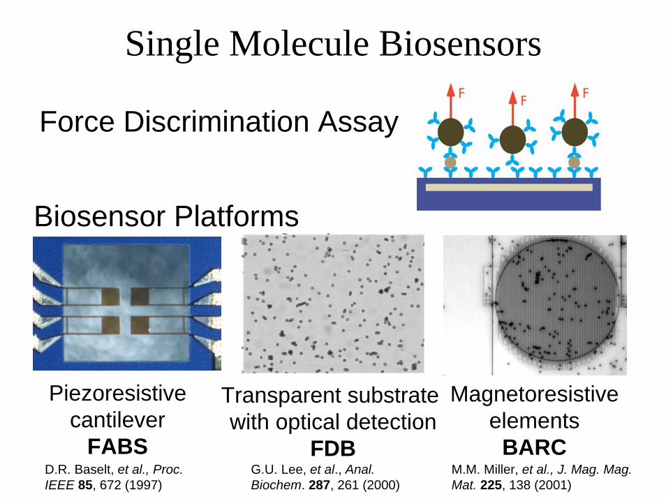
Single Molecule Biosensors
Biosensor Platforms
Piezoresistivecantilever
FABS
Transparent substrate with optical detection
FDB
Magnetoresistiveelements
BARCD.R. Baselt, et al., Proc. IEEE 85, 672 (1997)
G.U. Lee, et al., Anal. Biochem. 287, 261 (2000)
M.M. Miller, et al., J. Mag. Mag. Mat. 225, 138 (2001)
Force Discrimination Assay

Bead Array Counter
0
5
10
15
20
25
Sens
or S
igna
l (µV
)
15 min hybridization
10 fM ALF DNA0.7 µV signal
2.6% coverage
1 nM ALF DNA17.5 µV singal21% coverage
Chemical Bkgd = 0.4%Electrical Bkgd = 0.2 µV
Fabricated by NVE4.5 mm 200 µm
2 µm
4.5 mm 200 µm
2 µm
GMRSensor
GMRSensorSiSi33NN44
GoldSSSSSSSSSS S S S S S S S S S
PEG
Streptavidin
Probe DNABiotinylatedsample DNA
Mag.Bead
GMRSensor
GMRSensorSiSi33NN44
GoldSSSSSSSSSS S S S S S S S S S
PEG
Streptavidin
Probe DNABiotinylatedsample DNA
Mag.Bead
• Demonstrated sensitivity <1 fM in ~30 min total assay time
• Integrated prototype completed, licensed for environmental monitoring (Seahawk Biosystems)
J.C. Rife, et al., Sensors & Actuators A 107, 209 (2003)

Power Sources
Smart DustK. Pister, UC Berkeley
K.E. Swider-Lyons & coworkers, “Power Sources for Nanotechnology,”Int. J. Nanotechnology 1, 149 (2003)
NSF MPS-IC Workshop on Approaches to Combat Terrorism
19-21 Nov 2002
Opportunities for Basic Research in Energy and
Power Sources
http://www.nsf.gov/pubs/2003/nsf03569/nsf03569
.htm-
+ Li metal(Anode)
Thin film MnOx ambigel
(Cathode)
Polymer(Separator)
~ 10 nanometer
Replacing conventional battery architecture with new 3-dimensional nanostructured architecture …
…to achieve higher battery capacity and energy density
Conventional Battery
3-D NanoBattery
-
+ Li metal(Anode)
Thin film MnOx ambigel
(Cathode)
Polymer(Separator)
~ 10 nanometer
-
+ Li metal(Anode)
Thin film MnOx ambigel
(Cathode)
Polymer(Separator)
~ 10 nanometer~ 10 nanometer
Replacing conventional battery architecture with new 3-dimensional nanostructured architecture …
…to achieve higher battery capacity and energy density
Conventional Battery
3-D NanoBattery
D.R. Rolison & coworkers, Nature 406, 169-172 (2000)
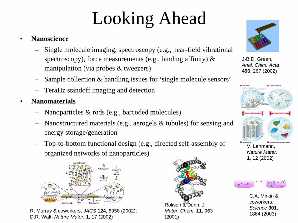
Looking Ahead• Nanoscience
– Single molecule imaging, spectroscopy (e.g., near-field vibrational spectroscopy), force measurements (e.g., binding affinity) & manipulation (via probes & tweezers)
– Sample collection & handling issues for ‘single molecule sensors’– TeraHz standoff imaging and detection
• Nanomaterials– Nanoparticles & rods (e.g., barcoded molecules)– Nanostructured materials (e.g., aerogels & tubules) for sensing and
energy storage/generation– Top-to-bottom functional design (e.g., directed self-assembly of
organized networks of nanoparticles)
Rolison & Dunn, J. Mater. Chem. 11, 963 (2001)
V. Lehmann, Nature Mater.1, 12 (2002)
R. Murray & coworkers, JACS 124, 8958 (2002); D.R. Walt, Nature Mater. 1, 17 (2002)
J-B.D. Green, Anal. Chim. Acta496, 267 (2002)
C.A. Mirkin & coworkers, Science 301, 1884 (2003)
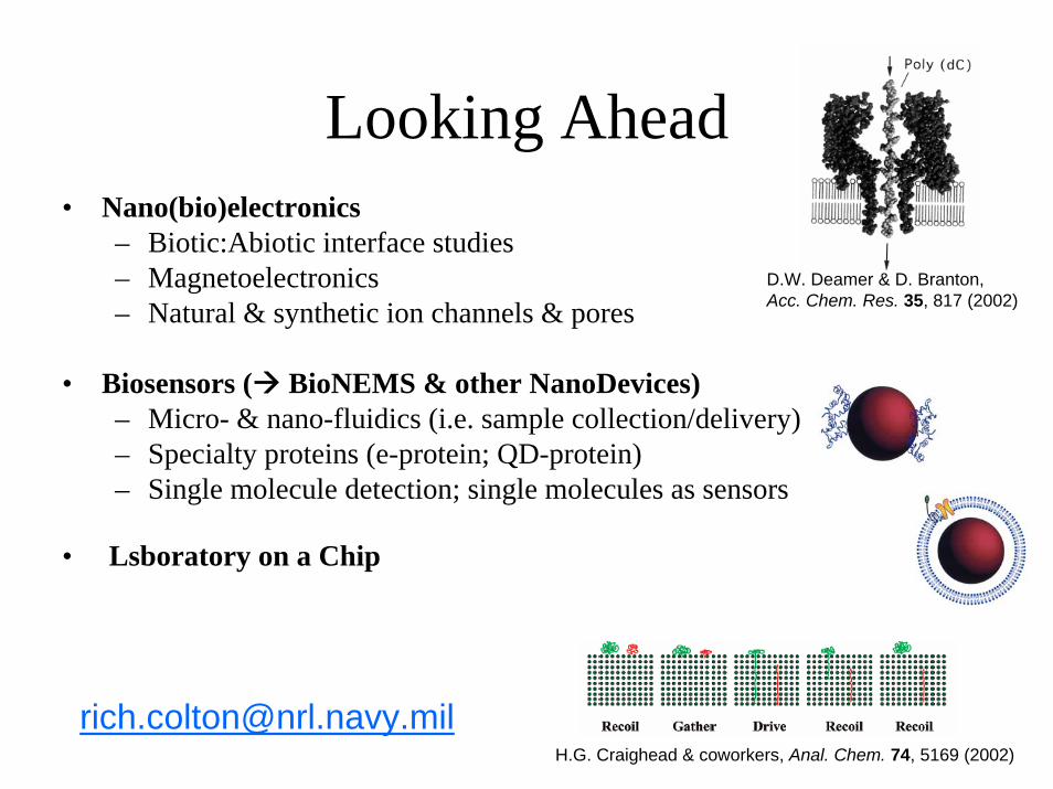
Looking Ahead• Nano(bio)electronics
– Biotic:Abiotic interface studies– Magnetoelectronics– Natural & synthetic ion channels & pores
• Biosensors ( BioNEMS & other NanoDevices)– Micro- & nano-fluidics (i.e. sample collection/delivery)– Specialty proteins (e-protein; QD-protein)– Single molecule detection; single molecules as sensors
• Lsboratory on a Chip
D.W. Deamer & D. Branton, Acc. Chem. Res. 35, 817 (2002)
[email protected]. Craighead & coworkers, Anal. Chem. 74, 5169 (2002)