Nanotechnology - Academia Sinica
68
Transcript of Nanotechnology - Academia Sinica

2nd week

Background
Solid state physicsQuantum physics Surface scienceSemiconductor physicsThin filmAnalytical chemistryPhysical chemistryPolymer scienceBiology
3

4
Cohesion of solids
Attractive electrostatic interaction between the negative charges of the electrons and the positive charges of the nuclei.The distribution of the outmost electrons and the ion cores.Specialized terms: Exchange interaction, van der Waals force and covalent bonds.

5
Van der Waals-London interaction
Dipole moments induce attractive interaction.Pauli exclusion principle induce repulsive interaction.The cohesive energy of an inert gas crystal is given by summing the Lennard-Jones potential over all pairs of atoms in the crystal.
φa - φbφa + φb
φa φb
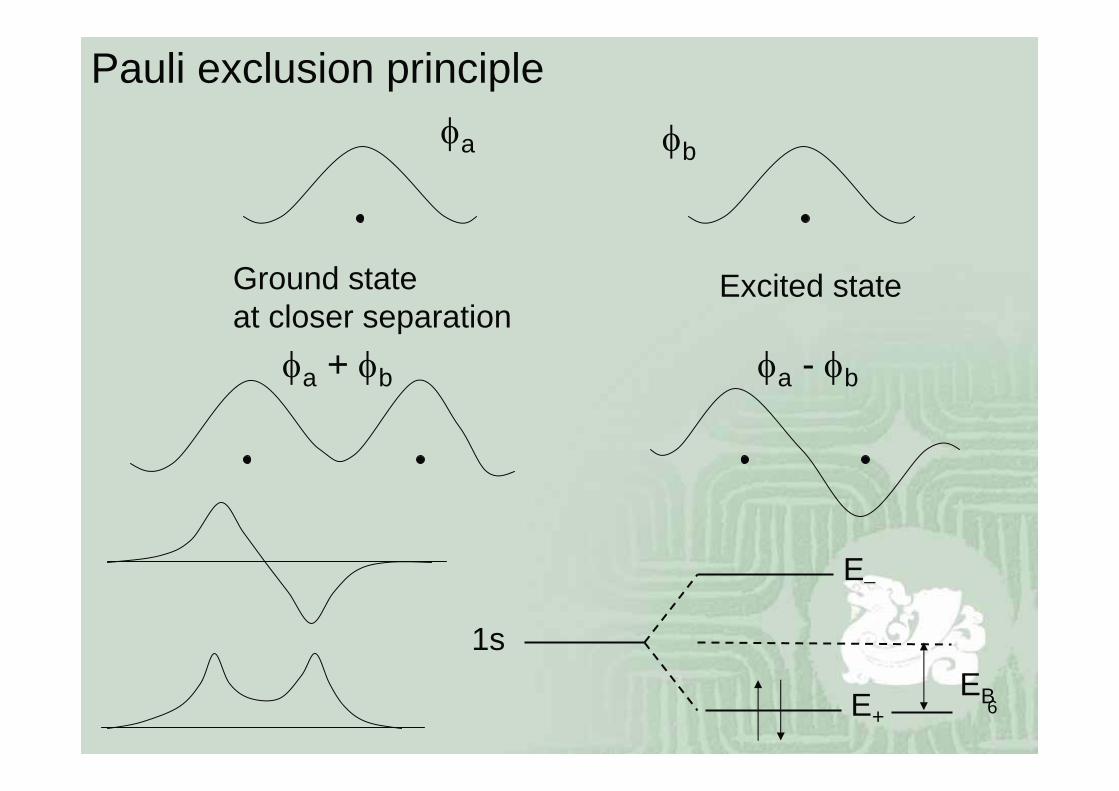
Pauli exclusion principle
Excited stateGround state at closer separation
1s
E+
E−
EB6

7
Lennard-Jones potential (interparticle interaction)
U = 4ε [ (σ/R)12 – (σ/R)6 ]
Repulsive core : R-12 Attractive tail : R-6

8
Crystals of inert gases
Simplest crystals, transparent insulators, weakly bound, with low melting temperatures.The outermost electron shells of the inert gas atoms are completely filled, and the distribution of electron charge in the free atom is spherically symmetric.In the crystal the inert gas atoms pack together as closely as possible: the crystal structure are all cubic closed-packed (fcc), except He3 and He4.
9
Ionic bonding
The ionic bond results from the electrostatic interaction of oppositely charged ions.The ions arrange themselves in whatever crystal structure gives the strongest attractive interaction compatible with the repulsive interaction at short distance between ion cores.

10
Covalent bond
The classical electron pairs or homopolarbond. It is a strong bond, strong direction, with atoms joined to four nearest neighbors at tetrahedral angles, even though this arrangement gives a low filling of space, 0.34 of the available space, compared with 0.74 for a close-packed structure.

11
Exchange interaction
Spin-dependent coulomb interaction.The strongest binding occurs when the spins of the two electrons are anti-parallel.The binding depends on the relative spin orientation not because there are strong magnetic dipole forces between the spins, but because the Pauli principle modifies the distribution of charge according to the spin orientation.

12
MetalsHigh electric conductivity, large number of electrons in a metal are free to move about, usually one or two per atom.The valence electrons of the atom become the conduction electrons of the metal.The bond formed by a conduction electron is not very strong.Metals tend to crystallize in relatively close packed structures: fcc, bcc, hcp.In transition metals there is additional binding from inner electron shells (d-electron shells).

13
Hydrogen bond
Ionic in character.It is an important part of the interaction between water molecules.It is important in certain ferroelectric crystals.

14
Energy bandElectrons in crystals are arranged in energy bands separated by regions in energy for which no wavelike electron orbital exist. Such forbidden regions are called energy gaps or band gaps.Large number of atoms are closed to each other and formed a crystal, their interaction with one another lead to a splitting of each of their energy levels and the energy levels will lie on a quasicontinuous scale, energy bands.The width of the band depends on the overlap of the wavefunctions (electron) concerned.

15Interatomic distance
15

16
EF
VB
CB
Insulators SemiconductorsMetals orsemimetals
Metals

Bulk Crystal Structures
2-D: 5 types, square, hexagonal, rectangular, centered rectangular (x2).3-D: 14 types, triclinic, monoclinic, orthorthombic, tetragonal, cubic, trigonal, hexagonal.Cubic: simple cubic, body-center cubic (bcc), face-center cubic (fcc).
17

Surface of Crystals
Surface: the few (2 - 10) outermost atomic layers (10 – 100 nm) of a solid. Surface dangling bonds, surface states, surface energy.Surface structure reconstruction, relaxation.Steps, defects.
18

Material analysis
Structure, morphology: XRD, SEM, TEM, luminescence (CL, PL), Raman.Composition: ICP-MS, Atomic absorption & emission spectrometry, XRF, FTIR, NMR.Surface & electronic structures: AES, XPS, RBS, SIMS, STM, AFM.Transport (electric conductivity): Hall effect, 4-point measurement.Magnetism: VSM, SQUID, EPR, FMR.
19

202020
NanostructuresWhen the extent of a solid is reduced in one or more dimensions, the physical, magnetic, electrical and optical properties can be dramatically altered.1 D: carbon nanotubes, quantum wires and conducting polymers.0 D: semiconductor nanocrystals, metal nanoparticles and lithographically patterned quantum dots.

21

22
Definition of NanoparticlesA particle with sufficiently small diameter for physical and chemical properties to differ measurably from those of the bulk material.Agglomerate: A group of particle held together by relatively weak forces, including Van der Waals forces, electrostatic forces and surface tension.Aggregate: A hetergeneous particle in which the various components are not easily broken apart.
23
Properties of Nanoparticles
Electronic structures: Discrete energy levels.Size effect: Quantum confinement, blue shift in optical absorption.Surface effect: Surface property dominant, surface catalysis.Shape effect: Specific stable shapes, structures.

24
Electronic structure of 0 D
Quantized energy levels: A system of electrons fully confined in all three dimensions will have discrete charge and electronic states, as do atoms and molecules.Eigenstates and eigenenergies: En,l,m = En,l; Ψ(r, θ, φ) = Yl,m(θ,φ) Rn,l(r).

2525
Changes of electronic density of states
26
Size effectsSpecific size effects: These involve self-selection and existence of magic numbers for small and moderately sized clusters and nanostructures.Smooth size effects for large nanostructures.Coulomb blockade: The staircase for the charging energy indicating the discrete electronic levels.Confinement: Boundary effects on electrons or excitons.

27

28
Optical absorption of CdSe

29
Size-dependent of optical absorption

30
Quantum confinement in nanocrystalline Si quantum dots
T. –W. Kim,APL 88, 123102 (2006).

31
Metallic dotsEnergy levels for small spherical alkali metallic cluster.

32
Coulomb-blockade charging energy

3333
Quantum Size Effects in Metallic Nanostructures
Physics Today April 2007, p50.In a thin film, the quantization of the wave functions divides the continuous band into discrete subbands.
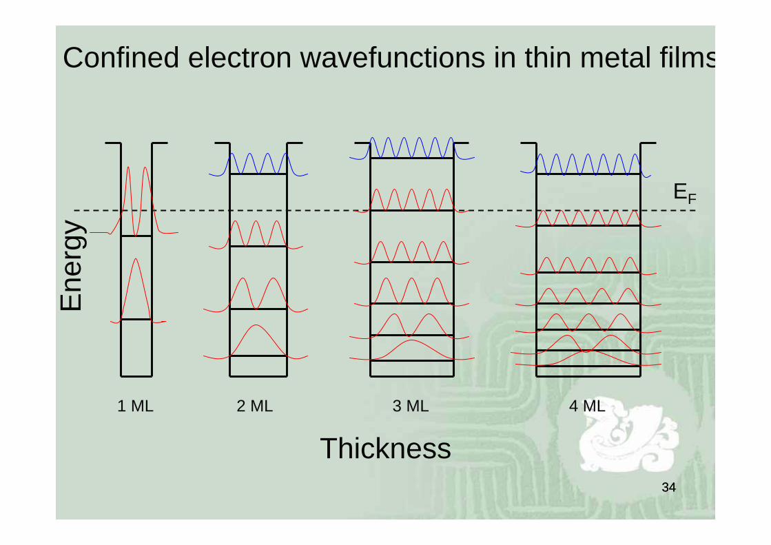
3434
1 ML 2 ML 3 ML 4 ML
Thickness
EF
Ene
rgy
Confined electron wavefunctions in thin metal films

3535
P. Moriarty, Rep. Prog. Phys. 64, 297, 2001.
(c) quantum mirages—the upper images are conventional topographic STM data whereas the lower images are dI/dV maps. In the topographic images on the left and right, an individual magnetic impurity (a Co atom) has been positioned within an elliptical corral formed from Co atoms. When the single Co atom is at a focus of the ellipse, the spectroscopic signature associated with the Kondo effect is projected to the other focus (the spectroscopic map on the left). When the Co atom is moved off focus the spectroscopic signature (the ‘quantum mirage’) vanishes the dI/dV map on the right) (Manoharan et al 2000). (d) Synthesis of individual molecular complexes. Both an FeCO and an Fe(CO)2 molecule have been synthesized (Lee and Ho 1999).

36
Shape effects
Symmetry-breaking: Structural deformations affect the electronic structure and charge density.Collective excitation: Shape deformation induced plasmon-collective vibration excitations.

37
Surface effect
Large ratio of number of surface atoms to bulk atoms in a nanostructure.For a spherical nanoparticle of radius R composed of atoms with an average spacing a, the ratio is Nsurf/N = 3a/R. For R = 6a ~ 1 nm, Nsurf/N ~ ½, half of the atoms are on the surface.
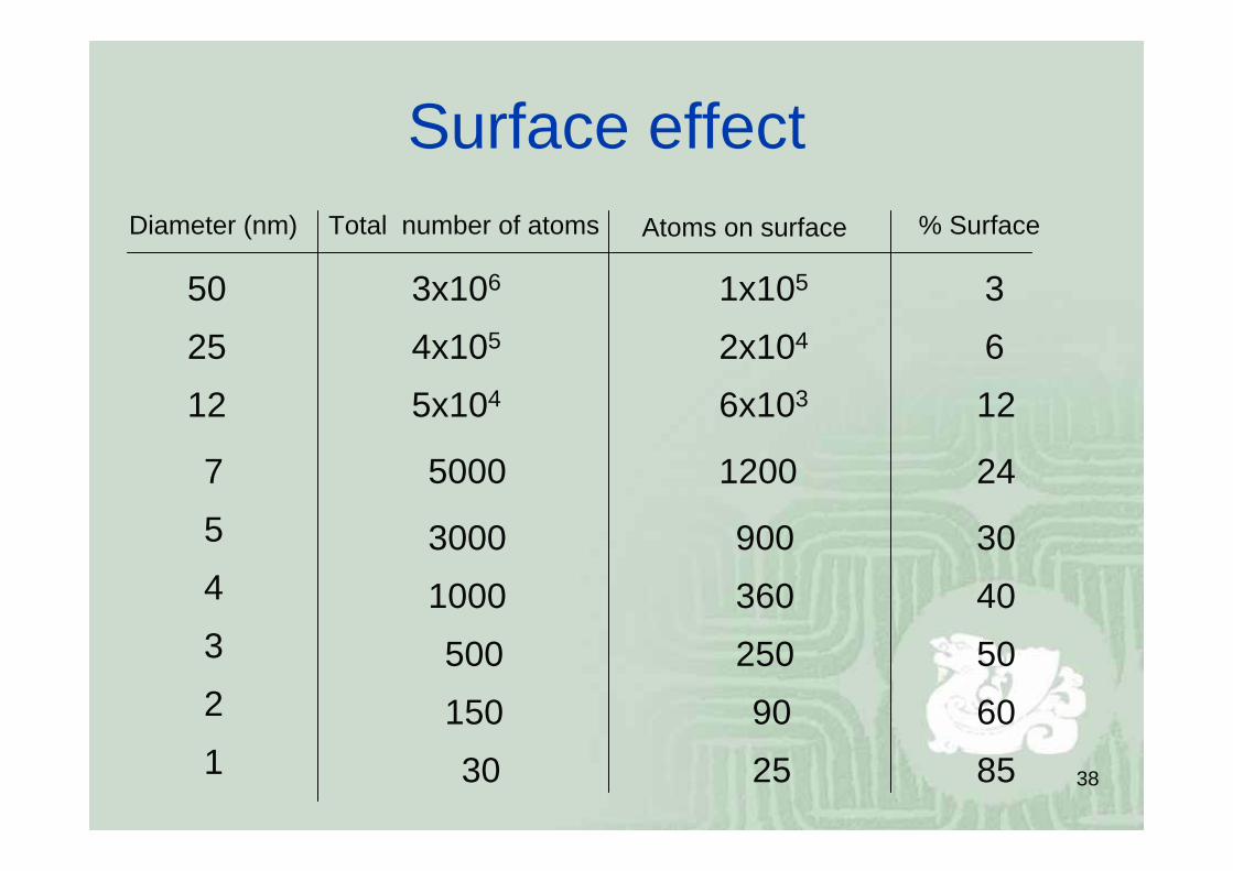
38
Surface effectDiameter (nm) Total number of atoms Atoms on surface % Surface
50 3x10⁶ 1x10⁵ 325 4x10⁵ 2x10⁴ 612 5x10⁴ 6x10³ 12
5 3000 900 30
7 5000 1200 24
4 1000 360 40321
50015030
2509025
506085

39

40
41

42
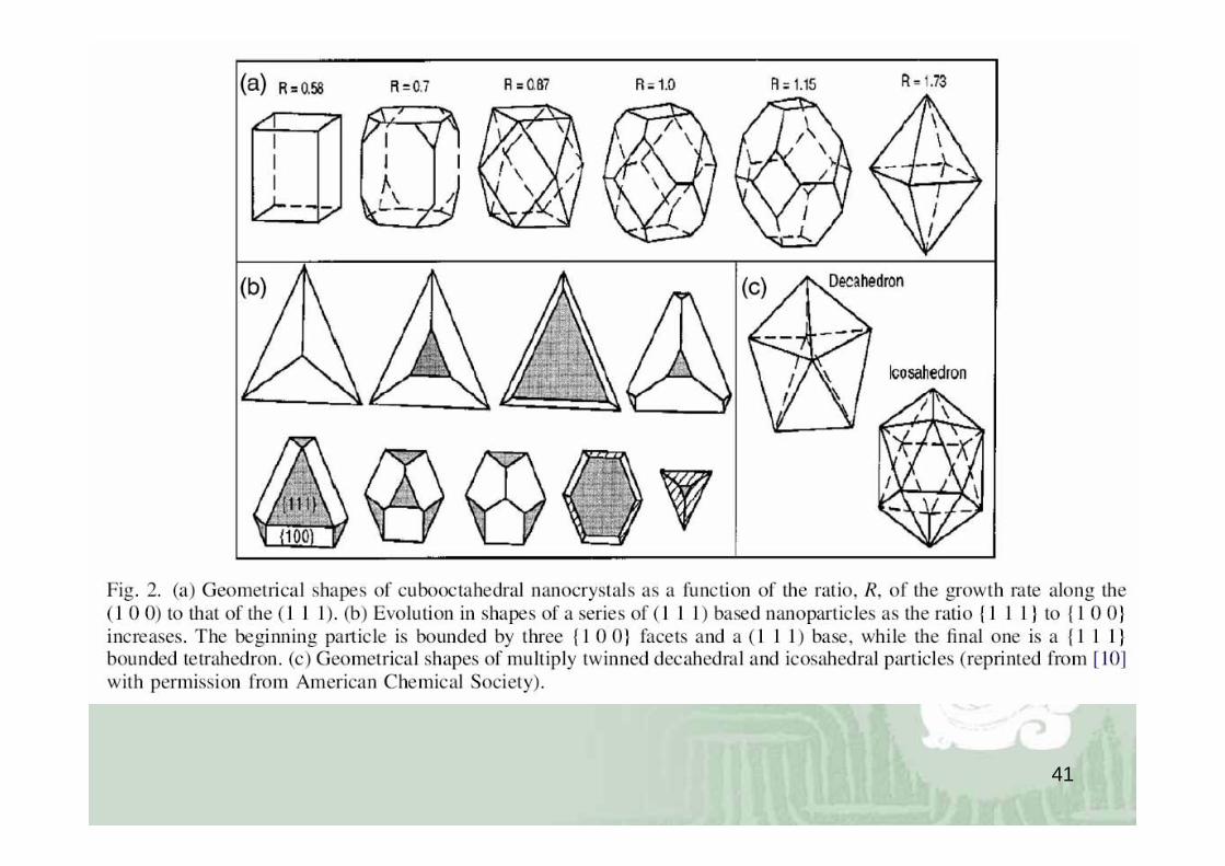
Face-centered-cubic clusters: (a) octahedron; (b) truncated octadedron; (c) cuboctahedron.
Nanocrystals

43
Icosahedral clusters.Clusters
Decahedral clusters: (a) regular decahedra; (b) Inotruncateddecahedra (Ino, 1969); (c) Marks truncated decahedra.

44Qualitative behavior of ∆ for crystalline,icosahedron, and decahedron clusters.
Energy
(# of atoms)
Stability of clusters

45
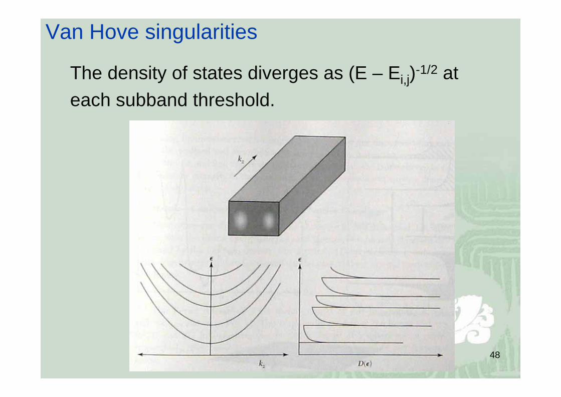
Electronic structure of 1 D
The quantized electronic states of nanostructures determine their electrical and optical properties, and they also influence the physical and chemical properties.The coulomb interactions between electrons cannot be ignored in nanostructures.

46
The energies and eigenstates in a wire, with x and y dimensions in nanoscale but continuous in z are given by:
E = Ei,j + ħ2k2/2m, Ψ (x, y, z) = Ψi,j(x,y)eikz
i, j are the quantum numbers labeling the eigenstates in the x, y plane and k is the wavevector in the z direction.
Nanowire

47
Desity of states of each subband is given by:
Di,j (E) = dNi,j/dE = (dNi,j/dk)(dk/dE)
= (2)(2)(L/2π)[m/2ħ2(E-Ei,j)]1/2
The total density of states is:
D(E) = ΣDi.j (E)i.j
For E > Ei,j= 4L/hνi,j
= 0 For E < Ei,j
Spin degeneracy
±k
νi,j: Velocity ofthe electron in thei, j subband withKinetic energyE – Ei,j.
48
Van Hove singularities
The density of states diverges as (E – Ei,j)-1/2 at each subband threshold.

49
Carbon nanotube(semiconducting)

50
Coulomb interaction
Coulomb interactions cause scattering among electrons near the Fermi energy.For 3D metals, scattering is strongly suppressed near EF by the restrictions of energy/momentum conservation combined with the Pauli exclusion principle.The ground state of the interacting 1D electron gas is believed not to be a Fermi liquid, but rather a Luttinger liquid whose low energy excitations are collective in nature (phonons or plasmons).

51
Electrical transport in 1 D
•Conductance quantization: Gq = 2e2/h.

52
Imaging techniques for nanostructures
Electron: Transmission electron microscopy (TEM), scanning electron microscopy (SEM), scanning tunneling microscopy (STM).Force: Atomic force microscopy (AFM), magnetic force microscopy (MFM).Photon: Near field optical microscopy.

53
Nanostructure fabrications
Bottom-up approach: Growth and self-assembly to build nanostructures from atomic or molecular precursors. (There is plenty of room at the bottom).Top-down approach: Lithographic patterning to structure macroscopic materials at the nanoscale. (“There is plenty of room at the top”, Jean-Marie Lehn).

54
Small
Big
Top-down Bottom-up

55
A schematic illustration of various thin-film growth modes (θ represents the total adsorbatecoverage). (a) Frank–van der Merwe (FM) growth—strict layer-by-layer epitaxial growth; (b) Stranski–Krastanov (SK) growth—growth occurs in a layer-by-layer (i.e. 2D) fashion up to a certain critical thickness (which is generally related to the lattice mismatch between the adsorbateand substrate materials) and then switches to a 3D, i.e. islanding growth mode;(c) Vollmer–Weber (VW) growth—this occurs when the adsorbate and substrate surface (andinterface) free energies are such that it is thermodynamically favourable for the overlayer to formislands from the onset of growth.

56

57
Controlling the shape of SK-grown nanocrystals
InAs clusters on GaAs(100) on GaAs(311)
InAs clusters
InP clusterson GaAs
Ge clusterson Si
5858
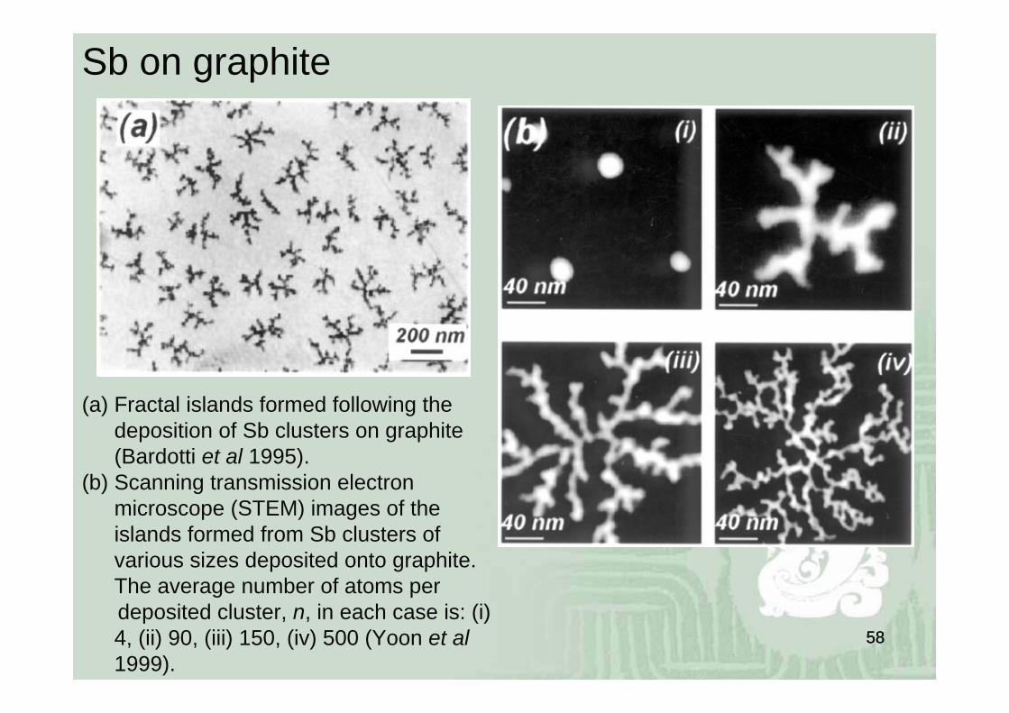
(a) Fractal islands formed following the deposition of Sb clusters on graphite (Bardotti et al 1995).
(b) Scanning transmission electron microscope (STEM) images of the islands formed from Sb clusters of various sizes deposited onto graphite. The average number of atoms perdeposited cluster, n, in each case is: (i) 4, (ii) 90, (iii) 150, (iv) 500 (Yoon et al 1999).
Sb on graphite

59
Lithography
Parallel: Optical, x-ray, ion-beam, extreme ultraviolet, imprint.Serial: E-beam, laser, focus ion beam.Other lithography: Microcontact printing, nanosphere lithography, scanning probe lithographies, dip-pen nanolithography, field induced oxidation, feedback controlled lithography.

60
Particle wavelength (A) at various energies
Particles 1 eV 10 eV 100 eV 1 KeV 10 KeV 100 KeV 1 MeV
Photon
Electron
Proton
12400 1240 124 12.4 1.24 0.124 0.012
12.3 3.89 1.23 0.39 0.12 0.037 0.0087
0.29 0.091 0.029 0.0091 0.0029 0.00091 0.00028
λ (A) = 12400/E ,Photon:
Electron: λ (A) = 12.3/E1/2
Proton: λ (A) = 0.29/E1/2
E (eV).

61

62

63
E-beam lithography

64
PMMA: polymethyl methacrylate;P(GMA-co-EA): poly(glycidyl methacrylate-co-ethyl acrylate;PBS: poly(butene-1-sulfone);COP: copolymer methyl methacrylate;PGMA: poly(glycidyl methacrylate;PCA: copolymer of α-cyano ethyl acrylateand α-amine ethyl acrylate
Organic E-beam Resist

65

66

67
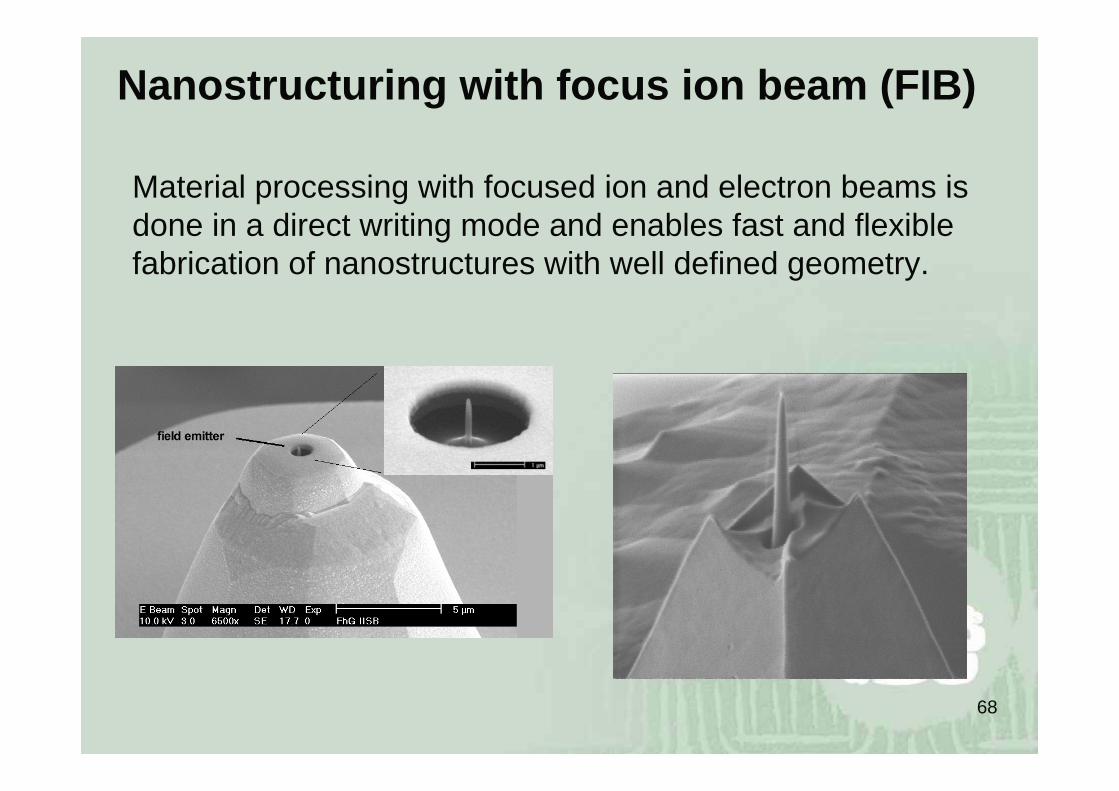
Focus Ion Beam (FIB)
68
Material processing with focused ion and electron beams is done in a direct writing mode and enables fast and flexible fabrication of nanostructures with well defined geometry.
Nanostructuring with focus ion beam (FIB)