Nanoscale RF CMOS Transceiver Design - TUC · Nanoscale RF CMOS Transceiver Design Angelos...
217
Objective LNA Design RF Test Chip FoM for RFIC Design Thermal Noise LNA Implementation Conclusions Nanoscale RF CMOS Transceiver Design Angelos Antonopoulos Department of Electronics & Computer Engineering Technical University of Crete February 23, 2014 1 / 65
-
Upload
nguyenkhanh -
Category
Documents
-
view
223 -
download
2
Transcript of Nanoscale RF CMOS Transceiver Design - TUC · Nanoscale RF CMOS Transceiver Design Angelos...
Objective LNA Design RF Test Chip FoM for RFIC Design Thermal Noise LNA Implementation Conclusions
Nanoscale RF CMOS Transceiver Design
Angelos Antonopoulos
Department of Electronics & Computer EngineeringTechnical University of Crete
February 23, 2014
1 / 65

Objective LNA Design RF Test Chip FoM for RFIC Design Thermal Noise LNA Implementation Conclusions
Optimum Bias Point for RFIC design w. Technology Scaling?
Optimum Region for RFIC Design?
Aggressive CMOS technology scaling down to 28 nm.
RFICs under low voltage/power operation.
Suitable region for RFIC design ?
High overall performance w. min. power consumption.
2 / 65

Objective LNA Design RF Test Chip FoM for RFIC Design Thermal Noise LNA Implementation Conclusions
Previous Work - Motivation
Open Issues
Taris et al., NanoTera 2011
OR ?
FoM = f (Gain,Noise,power , f ) ∝ (Gm/ID) · fT
C.-H. Chen, “Thermal noise in modernCMOS technologies,” in Solid StateCircuits Technologies, InTech, 2010.
Transistors might work in themoderate or weak inversionregion.
Channel noise models fortransistors working in these regions
Scaling issues of the active noisesources research area for futurestudies.
3 / 65

Objective LNA Design RF Test Chip FoM for RFIC Design Thermal Noise LNA Implementation Conclusions
Previous Work - Motivation
Open Issues
Figures of Merit representing RFIC behavior.
Simple and easy to evaluate.
Thermal noise in terms of RFIC design
Validation through RFIC design
IC = ID/Ispec
Ispec = 2nU2T µCox
WL
4 / 65

Objective LNA Design RF Test Chip FoM for RFIC Design Thermal Noise LNA Implementation Conclusions
This Work
Outline
System to Block
Receiver blocks
Circuit Level
LNA Topologies
Device Level
Tapeout of an RF Test Chip in 90nm CMOS
Measurements and De-embedding
Small-signal analysis
Figures of Merit (FoM) for LNA Design
Thermal Noise
RF noise trendsNoise parameters essential for LNA design
Verification with EKV3 model
Circuit Level
30 GHz LNA
5 GHz LNA based on FoM
Conclusions
5 / 65

Objective LNA Design RF Test Chip FoM for RFIC Design Thermal Noise LNA Implementation Conclusions
Receiver Architectures
Transceiver and Building Blocks
Receiver architectures
Heterodyne (IF, problem of image)Direct conversion (zero IF)
Noise of cascaded stages
NF = 1 + (NF1−1) +NF2−1AP1
+ NFm−1AP1 ...AP(m−1)
Non-linearity of cascaded stages
1A2IIP3
= 1A2IIP3,1
+α2
1A2IIP3,2
+α2
1 β21
A2IIP3,2A
2IIP3,3
LNA should provide
Minimum noise figureModerately high gain, depending onthe application
6 / 65

Objective LNA Design RF Test Chip FoM for RFIC Design Thermal Noise LNA Implementation Conclusions
LNA Requirements
LNA Requirements
Matching
Power matching
Maximum power transfer to a load
ZL = Z ∗SInput matching
Input impedance equal to 50 ΩReturn loss: Γ = Zin−RS
Zin+RSIdeally Γ = 0
Noise matching
YS = Yopt
Stability and Reverse Isolation
Feedback paths from the output to theinput may lead to instability
Stern stability factor
K = 1+|∆|2−|S11|2−|S22|22|S21||S12|
When K>1 andΔ<1 the circuit isunconditionally stable
Reverse isolation (-S12)
Improves stabilityReduces spurious LO tone at theantenna
7 / 65
Objective LNA Design RF Test Chip FoM for RFIC Design Thermal Noise LNA Implementation Conclusions
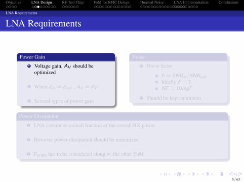
LNA Requirements
LNA Requirements
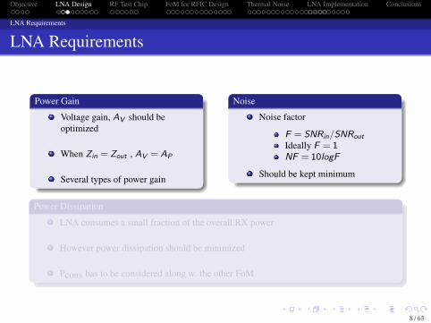
Power Gain
Voltage gain, AV should beoptimized
When Zin = Zout , AV = AP
Several types of power gain
Noise
Noise factor
F = SNRin/SNRoutIdeally F = 1NF = 10logF
Should be kept minimum
Power Dissipation
LNA consumes a small fraction of the overall RX power
However power dissipation should be minimized
Pcons has to be considered along w. the other FoM
8 / 65

Objective LNA Design RF Test Chip FoM for RFIC Design Thermal Noise LNA Implementation Conclusions
LNA Requirements
LNA Requirements
Power Gain
Voltage gain, AV should beoptimized
When Zin = Zout , AV = AP
Several types of power gain
Noise
Noise factor
F = SNRin/SNRoutIdeally F = 1NF = 10logF
Should be kept minimum
Power Dissipation
LNA consumes a small fraction of the overall RX power
However power dissipation should be minimized
Pcons has to be considered along w. the other FoM
8 / 65

Objective LNA Design RF Test Chip FoM for RFIC Design Thermal Noise LNA Implementation Conclusions
Existing topologies
LNA topologies
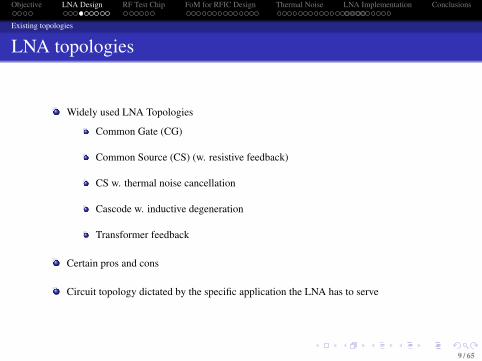
Widely used LNA Topologies
Common Gate (CG)
Common Source (CS) (w. resistive feedback)
CS w. thermal noise cancellation
Cascode w. inductive degeneration
Transformer feedback
Certain pros and cons
Circuit topology dictated by the specific application the LNA has to serve
9 / 65

Objective LNA Design RF Test Chip FoM for RFIC Design Thermal Noise LNA Implementation Conclusions
Existing topologies
LNA topologies
Widely used LNA Topologies
Common Gate (CG)
Common Source (CS) (w. resistive feedback)
CS w. thermal noise cancellation
Cascode w. inductive degeneration
Transformer feedback
Certain pros and cons
Circuit topology dictated by the specific application the LNA has to serve
9 / 65

Objective LNA Design RF Test Chip FoM for RFIC Design Thermal Noise LNA Implementation Conclusions
Existing topologies
Common Gate LNA
CG Stage w. Inductive Load
Input impedance
1/gms
Voltage gain
Av ≡ VoutVin
=R1
2RS
Thermal noise
F = 1 + γ + 4 RSR1
Limitation
Even if 4 RSR1 1 + γ , for γ=1, NF=3 dB
γ=1, very optimistic scenario
10 / 65

Objective LNA Design RF Test Chip FoM for RFIC Design Thermal Noise LNA Implementation Conclusions
Existing topologies
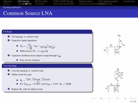
Common Source LNA
CS Stage
CS topology w. resistive load
Capacitive input impedance
Zin =RS
1+ jωωp
, ωp = 1RS (Cgs+MCgd )
Miller factor, M = 1 +gm1RL
Capacitive feedback from output to input through Cgd
Poor reverse isolation
Cascode Stage
Cascode topology w. resistive load
Suffers from low gain
RL <VDD−VDS,sat1−VDS,sat2
IDFor VDS,sat = 0.25V , and VDD = 1.2V , AV = 15dB
Replace RL with an inductor load
11 / 65
Objective LNA Design RF Test Chip FoM for RFIC Design Thermal Noise LNA Implementation Conclusions
Existing topologies
Common Source LNA
CS Stage
CS topology w. resistive load
Capacitive input impedance
Zin =RS
1+ jωωp
, ωp = 1RS (Cgs+MCgd )
Miller factor, M = 1 +gm1RL
Capacitive feedback from output to input through Cgd
Poor reverse isolation
Cascode Stage
Cascode topology w. resistive load
Suffers from low gain
RL <VDD−VDS,sat1−VDS,sat2
IDFor VDS,sat = 0.25V , and VDD = 1.2V , AV = 15dB
Replace RL with an inductor load
11 / 65

Objective LNA Design RF Test Chip FoM for RFIC Design Thermal Noise LNA Implementation Conclusions
Existing topologies
Common Source LNA
CS Stage w. Resistive Feedback
RF senses the output voltage and returns a current to the input
Capacitive component due to Cgs still present
RF contributes to noise
F = 1 + 4 RSRF
+ γ(gm1 +gm2)RSNF exceeds 3 dB
CS Stage w. Noise Cancellation
Based on CS w. resistive feedback
Noise currents at points X and Y have equal sign
Signal voltages at X and Y have opposite signs
Noise cancellation
Vout,n = VY ,n−VX ,nAV⇒Avc =VY ,nVX ,n
= 1 +RFRS
AVFc = VoutVX
=−2 RFRS
12 / 65

Objective LNA Design RF Test Chip FoM for RFIC Design Thermal Noise LNA Implementation Conclusions
Existing topologies
Transformer Feedback LNA
Transformer Feedback LNA
Cgd canceled through an additional path from output to input
Cancellation whennk =
CgsCgd
n =√L22/L11
k = M/√L11L22
L11 used for source degeneration as well
k affects gain, input and output impedance
Complex equations
13 / 65

Objective LNA Design RF Test Chip FoM for RFIC Design Thermal Noise LNA Implementation Conclusions
Existing topologies
Cascode LNA w. Inductive Degeneration
Cascode Stage w. Inductive Degeneration
Input impedance
Zin = 1sCgs + s(LS +LG ) + ωT LS
LS is chosen so that Real(Zin) = 50ΩLG is chosen so that Imag(Zin) = 0Zin purely reactive at ω0
Voltage gain
AV ≡VoutVin
=ωT2ω0· RLRS
Improves w. technology scaling
Noise factor
F = 1 +gmγRS (ω0ωT
)2
Power constrained noise optimization
Wopt,P ' 13ωLCox RS
Power constrained simultaneous noise impedance matching (SNIM)
Extra capacitance in parallel w. Cgs
14 / 65

Objective LNA Design RF Test Chip FoM for RFIC Design Thermal Noise LNA Implementation Conclusions
Implementation
Tapeout of an RF Test Chip
90 nm CMOS from TSMC
Chip area 3.5mm2
RF structures
10 n-MOS, 10 p-MOSMultifingerL = 240nm − 100nm
Two port network
15 / 65

Objective LNA Design RF Test Chip FoM for RFIC Design Thermal Noise LNA Implementation Conclusions
Implementation
Tapeout of an RF Test Chip
90 nm CMOS from TSMC
Chip area 3.5mm2
RF structures
10 n-MOS, 10 p-MOSMultifingerL = 240nm − 100nm
Two port network
15 / 65

Objective LNA Design RF Test Chip FoM for RFIC Design Thermal Noise LNA Implementation Conclusions
Implementation
Tapeout of an RF Test Chip
90 nm CMOS from TSMC
Chip area 3.5mm2
RF structures
10 n-MOS, 10 p-MOSMultifingerL = 240nm − 100nm
Two port network
15 / 65

Objective LNA Design RF Test Chip FoM for RFIC Design Thermal Noise LNA Implementation Conclusions
Measurements
RF and Noise Measurements
Schroter & Sakalas, TU Dresden
Chuck Coa
x s
witc
h
26-50 GHz
Amplifier
Network
Analyzer
PNAP1 P2
DUTGSG 50 GHz Probe
Tuner
MT984A
WG sw
itchLoad
Semiconductor
Parametzer Analyzer
SMU2SMU1
Coax switch changes S
paramater path to noise
measurement path amd plus CW power for
LO path!
2.4mm connector 50
GHz Gore Cable40cm
2.41mm connector 50
GHz Gore Cable40 cm
Nois
e s
ourc
e1G
Hz-5
0 G
Hz
Pulsed DC
28V
Impedance
Tuner Controller
Coax switch changes S
paramater path to noise source
path.
BUScable
Maury , ICCAP
32
RF, DC and Noise 8 -50 GHz noise/lopad pull measurement system
GSG 50 GHz Probe
Coax sw
itch
LO
Drive
Am
plif
ier
OU
TLO IN
Amplifier
1-26 GHzNoise Figure
Meter
TRIAX
Bias
Tee
Bias
Tee
TRIA
XIF 1-26 GHz
A
B
C
26-50 Hz Filter
Atte
nu
ato
r
Attenuator
CEDIC Laboratory Master plan Part 2
Prober PM 5: High frequency standard and special measurements
1. Noise Figure meter , Spectrum analyzer Agilent E 4448 A
2. PM 5
3. PNA 8361 C
4. RF switch, LNA, downconverer
5. RF switch
6. Tuner Maury MT 984A 8-50 GHz
7. Impedance Tuner controller
8. Set of waveguides (missing, SFB)
9. 75-110GHz WG-Coax adapter x2 (missing, SFB)
10. 75-110 GHz waveguide probes with BT (missing)
11. 75-110 GHz wg switch x2 (missing)
12. 75-110 GHz isolator x2 (missing)
13. 1GHz RF Gore cable x2 (40cm) missing
14. 75-110 GHz load (missing)
15. RF power amplifier (75-110 GHz) missing
16. LNA for noise parameter (NP) meas. (missing)
17. Downconverter for NP meas. 75-110 GHz to 1-26 GHz
(missing)
PM 5
1
2
3
4
5
6
7
16 / 65

Objective LNA Design RF Test Chip FoM for RFIC Design Thermal Noise LNA Implementation Conclusions
De-embedding
RF and Noise De-embedding
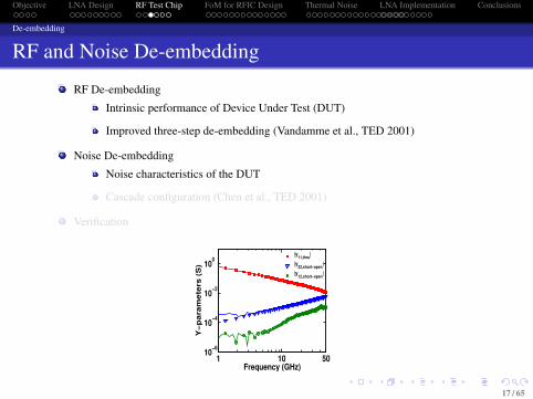
RF De-embedding
Intrinsic performance of Device Under Test (DUT)
Improved three-step de-embedding (Vandamme et al., TED 2001)
Noise De-embedding
Noise characteristics of the DUT
Cascade configuration (Chen et al., TED 2001)
Verification
1 10 5010
−6
10−4
10−2
100
Frequency (GHz)
Y−
para
mete
rs (
S)
|y11,thru
|
|y22,short−open
|
|y12,short−open
|
17 / 65

Objective LNA Design RF Test Chip FoM for RFIC Design Thermal Noise LNA Implementation Conclusions
De-embedding
RF and Noise De-embedding
RF De-embedding
Intrinsic performance of Device Under Test (DUT)
Improved three-step de-embedding (Vandamme et al., TED 2001)
Noise De-embedding
Noise characteristics of the DUT
Cascade configuration (Chen et al., TED 2001)
Verification
1 10 5010
−6
10−4
10−2
100
Frequency (GHz)
Y−
para
mete
rs (
S)
|y11,thru
|
|y22,short−open
|
|y12,short−open
|
17 / 65

Objective LNA Design RF Test Chip FoM for RFIC Design Thermal Noise LNA Implementation Conclusions
De-embedding
RF De-embedding Results
NMOS (L = 100nm, W = 40x2um, VGS = 0.65V , VDS = 1.2V )
10−1
100
101
102
101
102
ID
/Ispec (−)
f T (
GH
z)
De−embedded
Measured
10−2
100
101
102
101
102
ID
/Ispec
(−)
f max (
GH
z)
De−embedded
Measured
PMOS (L = 100nm, W = 40x2um, VGS =−0.65V , VDS =−1.2V )
10−1
100
101
102
100
101
102
ID
/Ispec (−)
f T (
GH
z)
De−embedded
Measured
10−1
100
101
102
102
ID
/Ispec
(−)
f max (
GH
z)
De−embedded
Measured
18 / 65

Objective LNA Design RF Test Chip FoM for RFIC Design Thermal Noise LNA Implementation Conclusions
De-embedding
Noise De-embedding Results
NMOS (L = 100nm, W = 40x2um, VGS = 0.65V , VDS = 1.2V )
8 10 12 14 16 18 200
1
2
3
Frequency (GHz)
NF
min
(d
B)
De−embedded
Measured
8 10 12 14 16 18 200
0.5
1
1.5
2
Frequency (GHz)
Rn
/50 (
−)
De−embedded
Measured
8 10 12 14 16 18 200.2
0.4
0.6
0.8
1
Frequency (GHz)
Mag
(Γo
pt)
(−)
De−embedded
Measured
8 10 12 14 16 18 200
20
40
60
80
100
Frequency (GHz)
∠Γ
op
t (d
eg
)
De−embedded
Measured
19 / 65

Objective LNA Design RF Test Chip FoM for RFIC Design Thermal Noise LNA Implementation Conclusions
De-embedding
Noise De-embedding Results
PMOS (L = 100nm, W = 40x2um, VGS =−0.65V , VDS =−1.2V )
8 10 12 14 16 18 200
1
2
3
4
5
Frequency (GHz)
NF
min
(d
B)
De−embedded
Measured
8 10 12 14 16 18 200
0.5
1
1.5
2
2.5
3
Frequency (GHz)
Rn
/50 (
−)
De−embedded
Measured
8 10 12 14 16 18 200.2
0.4
0.6
0.8
1
Frequency (GHz)
Mag
(Γo
pt)
(−)
De−embedded
Measured
8 10 12 14 16 18 200
20
40
60
80
100
Frequency (GHz)
∠Γ
op
t (d
eg
)
De−embedded
Measured
20 / 65

Objective LNA Design RF Test Chip FoM for RFIC Design Thermal Noise LNA Implementation Conclusions
HF Modeling
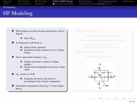
HF Modeling
With frequency increase design characteristics start todegrade
Gain, NFmin
At frequencies well below fT
(Quasi) Static operationImmediate current response to every voltagechange
Above quasi-static frequency,Ωqs
Charges need time to adjust to voltagechangesCharge density dependent on the past voltagevalues
Ωqs stands as a FoM
Frequency the device can reach wo.accounting for the extrinsic components
Performance degradation whenΩqs 5-7 times higherthan f0
MOS extrinsic part
Significant w. frequency increase
Connection between intrinsic and extrinsic parts
Source-drain extensionsParasitic resistances RS and RD
Simple equivalent circuit
Experiences limitations
21 / 65
Objective LNA Design RF Test Chip FoM for RFIC Design Thermal Noise LNA Implementation Conclusions
HF Modeling
HF Modeling
With frequency increase design characteristics start todegrade
Gain, NFmin
At frequencies well below fT
(Quasi) Static operationImmediate current response to every voltagechange
Above quasi-static frequency,Ωqs
Charges need time to adjust to voltagechangesCharge density dependent on the past voltagevalues
Ωqs stands as a FoM
Frequency the device can reach wo.accounting for the extrinsic components
Performance degradation whenΩqs 5-7 times higherthan f0
MOS extrinsic part
Significant w. frequency increase
Connection between intrinsic and extrinsic parts
Source-drain extensionsParasitic resistances RS and RD
Simple equivalent circuit
Experiences limitations
21 / 65

Objective LNA Design RF Test Chip FoM for RFIC Design Thermal Noise LNA Implementation Conclusions
Figures of Merit
Y-Parameters
Y-parameters: convenient way to extract FoM and device parameters
Y11 ∼= ω2RGC2G + jωCG
Y12 ∼=−ω2RGCGDCG − jωCGDY21 ∼= Gm−ω2RGCG (CGD +Cm)− jω(CGD +Cm)Y22 ∼= Gds + ω2RG (CGCBD +CGCGD +CGDCm) + jω(CBD +CGD)
CG = Imag(Y11)ω
CGD = Imag(Y12)ω
RG = Real(Y11)(Imag(Y11))2
22 / 65

Objective LNA Design RF Test Chip FoM for RFIC Design Thermal Noise LNA Implementation Conclusions
Figures of Merit
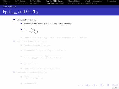
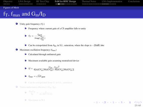
fT, fmax and Gm/ID
Unity gain frequency (fT )
Frequency where current gain of a CS amplifier falls to unity
fT =fspot
Imag(Y11Y21
)
Can be extrapolated from h21 in S.I., saturation, where the slope is −20dB/dec
Maximum oscillation frequency (fmax)
Calculated through unilateral gain
Maximum available gain assuming neutralized device
U =|Y21−Y12 |2
4[real(Y11)Real(Y22)−Real(Y12)Real(Y21)]
fmax =√Uf spot
Can be extrapolated from U, in S.I., saturation
Transconductance efficiency (Gm/ID )
GmUTID
= 2n(√
4IC+1+1)
Maximum in W.I.
23 / 65

Objective LNA Design RF Test Chip FoM for RFIC Design Thermal Noise LNA Implementation Conclusions
Figures of Merit
fT, fmax and Gm/ID
Unity gain frequency (fT )
Frequency where current gain of a CS amplifier falls to unity
fT =fspot
Imag(Y11Y21
)
Can be extrapolated from h21 in S.I., saturation, where the slope is −20dB/dec
Maximum oscillation frequency (fmax)
Calculated through unilateral gain
Maximum available gain assuming neutralized device
U =|Y21−Y12 |2
4[real(Y11)Real(Y22)−Real(Y12)Real(Y21)]
fmax =√Uf spot
Can be extrapolated from U, in S.I., saturation
Transconductance efficiency (Gm/ID )
GmUTID
= 2n(√
4IC+1+1)
Maximum in W.I.
23 / 65

Objective LNA Design RF Test Chip FoM for RFIC Design Thermal Noise LNA Implementation Conclusions
Figures of Merit
FoM for LNA Design
FoM(Gm/ID)fT
Transconductance frequency product (TFP)
TFP = (Gm/ID) · fT
Used to optimize low-power circuits(Mangla et al., MJ 2013)
Stands as a FoM for LNA design
FoMLPLNA = GV fRF(F−1)Pcons
(Gm/ID)fT in CS LNA
Vin
-GV ∝ gmCgsRSω
|@ωRF
-Pcons ∝ ID
-Fmin |MOS ∝ 1 + 1gmRS
⇒ FoM|LPLNA ∝gmfTID
24 / 65

Objective LNA Design RF Test Chip FoM for RFIC Design Thermal Noise LNA Implementation Conclusions
Figures of Merit
G2m/ID and GTFP
G2m/ID
Recently (Song et al., EDL, 2008) it was shown that excluding fRF
FoMLPLNA = GP(F−1)Pcons ∝ (G2
mID
)2
Representative of cascode topology
Easy to evaluate from DC measurements
Has not been studied w. length scaling
GTFP
Combines TFP w. intrinsic voltage gain
GTFP = TFP( GmGds
)
Gm/Gds decreases w. length scaling
25 / 65

Objective LNA Design RF Test Chip FoM for RFIC Design Thermal Noise LNA Implementation Conclusions
Figures of Merit
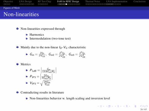
Non-linearities
Non-linearities expressed through
HarmonicsIntermodulation (two-tone test)
Mainly due to the non-linear ID-VG characteristic
Gm = ∂ ID∂VGS
, Gm2 = ∂ 2ID∂V 2
GS, Gm3 = ∂ 3ID
∂V 3GS
Metrics
P1dB =∣∣∣ Gm
13.8Gm3RS
∣∣∣PIP3 =
∣∣∣ 2Gm3Gm3RS
∣∣∣VIP3 =
√24GmGm3
Contradicting results in literature
Non-linearities behavior w. length scaling and inversion level
26 / 65

Objective LNA Design RF Test Chip FoM for RFIC Design Thermal Noise LNA Implementation Conclusions
Figures of Merit
Non-linearities
Non-linearities expressed through
HarmonicsIntermodulation (two-tone test)
Mainly due to the non-linear ID-VG characteristic
Gm = ∂ ID∂VGS
, Gm2 = ∂ 2ID∂V 2
GS, Gm3 = ∂ 3ID
∂V 3GS
Metrics
P1dB =∣∣∣ Gm
13.8Gm3RS
∣∣∣PIP3 =
∣∣∣ 2Gm3Gm3RS
∣∣∣VIP3 =
√24GmGm3
Contradicting results in literature
Non-linearities behavior w. length scaling and inversion level
26 / 65

Objective LNA Design RF Test Chip FoM for RFIC Design Thermal Noise LNA Implementation Conclusions
Results and Discussion
TCAD Verification
FoM presented versus
Measured data for the 90 nm case
TCAD data for technology nodes of L=180, 90, 45, 22 nm
Verified w. EKV3
Validated w. measurements from other groups and ITRS 2011
10 20 50 100 18010
1
102
103
Channel length (nm)
f T (
GH
z)
line: fT ∝ 1/L
TCAD
[8], [44], [53], [54]
[6]
ITRS 2011
Measured, this work
10 20 50 100 18010
1
102
103
Channel length (nm)
f max (
GH
z)
TCAD
[1], [53]
[6]
ITRS 2011
Measured, this work
Antonopoulos et al., TED, 2013
27 / 65

Objective LNA Design RF Test Chip FoM for RFIC Design Thermal Noise LNA Implementation Conclusions
Results and Discussion
h21 and U
Measured (L = 100nm,W = 10x2um, VDS = 1V )
109
1010
1011
1012
0
10
20
30
40
50
Frequency (Hz)
H2
1 (
dB
)
−20dB/dec
109
1010
1011
1012
0
10
20
30
40
50
Frequency (Hz)U
(d
B)
−20dB/dec
28 / 65

Objective LNA Design RF Test Chip FoM for RFIC Design Thermal Noise LNA Implementation Conclusions
Results and Discussion
fT and fmax
TCAD and measured (W = 10x2um, VDS = 0.9V )
10−1
100
101
102
100
200
300
400
500
ID
/Ispec
(−)
fT (
GH
z)
TCAD 180 nm
TCAD 90nm
Meas 90nm
TCAD 45nm
TCAD 22nm
Model
10−1
100
101
102
0
200
400
600
800
ID
/Ispec
(−) f
max (
GH
z)
TCAD 180 nm
TCAD 90nm
Meas 90nm
TCAD 45nm
TCAD 22nm
Model
29 / 65

Objective LNA Design RF Test Chip FoM for RFIC Design Thermal Noise LNA Implementation Conclusions
Results and Discussion
(Gm/ID)fT and G2m/ID
Measured (W = 40x2um, VDS = 1V )
10−1
100
101
102
101
102
103
ID
/Ispec
(−)
(Gm
/ID
)*f T
(G
Hz/V
)
L=240nm
L=180nm
L=120nm
L=100nm
10−1
100
101
102
10−2
10−1
100
Gm2
/ID
(S
2/A
)
ID
/Ispec
(−)
L=240nm
L=180nm
L=100nm
10−1
100
101
102
101
102
103
ID
/Ispec
(−)
(Gm
/ID
)*f T
(G
Hz/V
)
W=40 x 2 umV
DS=1 V
NMOS
PMOS
30 / 65

Objective LNA Design RF Test Chip FoM for RFIC Design Thermal Noise LNA Implementation Conclusions
Results and Discussion
(Gm/ID)fT , G2m/ID and GTFP
TCAD and measured (W = 10x2um, VDS = 0.9V )
10−1
100
101
102
102
103
104
ID
/Ispec
(−)
Gm
/ID
*fT (
TF
P)
(GH
z/V
)
10−1
100
101
102
0
0.5
1
Gm2
/ID
(S
2/A
)
ID
/Ispec
(−)
L=180nm
L=90nm
L=45nm
L=22nm
10−1
100
101
102
103
104
ID
/Ispec
(−)
Gm
/ID
*Gm
/Gd
s*f
T (
GT
FP
) (G
Hz/V
)
0.02 0.04 0.06 0.08 0.1
1e4m
ax
(GT
FP
) (G
Hz/V
)
VEFF
=VGS
−VT (V)
22nm45nm
90nm
180nm
22nm45nm
90nm180nm
0.02 0.04 0.06 0.08 0.11e2
1e3
1e4
ma
x(T
FP
) (G
Hz/V
)
31 / 65

Objective LNA Design RF Test Chip FoM for RFIC Design Thermal Noise LNA Implementation Conclusions
Results and Discussion
Non-Linearities
Measured (W = 40x2um, VDS = 1V , @f = 1.1GHz )
10−2
10−1
100
101
102
10−3
10−2
10−1
100
101
102
103
104
ID
/Ispec
(−)
Gm
(mS)
Gm2
(mS/V)
Gm3
(mS/V2)
10−2
10−1
100
101
102
−30
−20
−10
0
10
ID
/Ispec
(−)
P1
dB
(d
Bm
)
L=100nm
L=240nm
10−2
10−1
100
101
102
−20
−10
0
10
20
ID
/Ispec
(−)
PIP
3 (
dB
m)
L=100nm
L=240nm
10−2
10−1
100
101
102
10−1
100
101
ID
/Ispec
(−)
VIP
3 (
V)
L=100nm
L=240nm
Antonopoulos et al., RFIC Symp., 2013
32 / 65

Objective LNA Design RF Test Chip FoM for RFIC Design Thermal Noise LNA Implementation Conclusions
Results and Discussion
Non-Linearities
TCAD (W = 10x2um, VDS = 0.9V )
10−2
10−1
100
101
102
−30
−20
−10
0
10
ID
/Ispec
(−)
P1
dB
(d
B)
L = 180 nm
L = 45 nm
L = 22 nm
10−2
10−1
100
101
102
−20
−10
0
10
20
ID
/Ispec
(−)P
IP3 (
dB
)
L = 180 nm
L = 45 nm
L = 22 nm
33 / 65

Objective LNA Design RF Test Chip FoM for RFIC Design Thermal Noise LNA Implementation Conclusions
Contribution
Conclusions on Small-Signal Analysis and LNA Performance
Trends in FoMs investigated vs.
Bias, L, and technology
Individual FoM show a shift to lower inversion level w. length scaling
Combined FoM show the same shift
Optimum LNA performance studied via (Gm/ID) · fT and G2m/ID
Experience the same behaviorOptimum value achieved in M.I.
Contribution
Optimum RF performance shifted toward around-threshold operation as planar bulkCMOS scales down to 22 nm
34 / 65

Objective LNA Design RF Test Chip FoM for RFIC Design Thermal Noise LNA Implementation Conclusions
Basics of Thermal Noise
Noise in Semiconductors
Random process
Even if the past values are known, the instantaneous value cannot be predicted
Power spectral density
Characterizes the average power the signal carries
Noise in a resistor: Representations
Norton equivalent: Svn (f ) = V 2n = 4kTR1 (V 2/Hz)
Thevenin equivalent: SIn (f ) = I2n = V 2n/R2
1 = 4kT/R1 (A2/Hz)
MOS Transistors
Flicker (1/f ) noiseThermal noiseInduced gate noise
35 / 65

Objective LNA Design RF Test Chip FoM for RFIC Design Thermal Noise LNA Implementation Conclusions
Basics of Thermal Noise
Thermal Noise in MOSTs: A Short History
Hot research topic
Many groups (Birbas & Triantis, Enz & Roy, Schroter & Sakalas, Smit &Scholten, Deen & Chen,...)
Compact models (BSIM, PSP, EKV)
Noise description as a function of geometry, bias, scalingControversies in literature
Discrepancies
Excess noise in short devices and short channel effects (SCE)Noise parameters
Necessity to translate noise behavior of the device to circuit design
A lot of issues remain unclear and need to be clarified
36 / 65
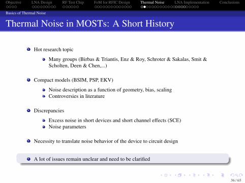

Objective LNA Design RF Test Chip FoM for RFIC Design Thermal Noise LNA Implementation Conclusions
The EKV3 Approach
Thermal Noise in MOSTs: The EKV3 Model
Thermal noise due to local random fluctuations of the carrier velocity
Transferred to the device terminalsModeled as a random current added to the DC local current
Modeling approach
Local noisy sourcex and x+Δx from SourceL-x and L-(x+Δx) from DrainNoisy current source in parallel withΔRTransistor is split into T1 and T2Channel conductance: 1
Gch= 1
G1+ 1
G2Drain fluctuation due to local noise source: δ InD = Gch∆Rδ InPSD of drain current due to all noisy sources:
S∆In2
D(ω) =
∫ L0 G2
ch∆R2S
δ I2n(ω,x)
∆x dx
Modeling approach applicable to frequencies well beyond fT
37 / 65
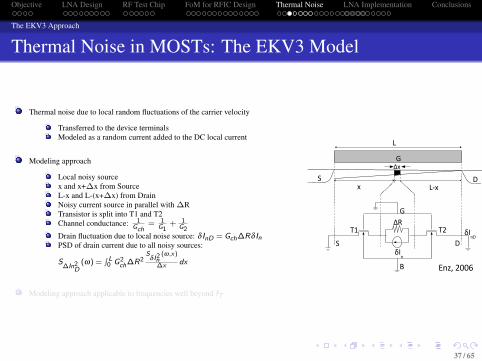

Objective LNA Design RF Test Chip FoM for RFIC Design Thermal Noise LNA Implementation Conclusions
The EKV3 Approach
Thermal Noise of Long Channel Devices
Constant carrier mobility, μ
PSD of drain noise currentID = µW (−Qi )
dVdx
Gch =dIDdV = µ(−Qi )
WL
∆R = ∆VID
= ∆xW µ(−Qi )
Due to local noise source δIn: Sδ I2nD
(ω,x) = G2ch(x)∆R2(x)S
δ I2n(ω,x)
Due to all noise sources: S∆I2nD
(ω) =∫ L0 ( ∆x
L )2S
δ I2n (ω,x)∆x dx = 1
L2∫ Lo ∆xS
δ I2n(ω,x)dx
Introduction of noise conductance GnD
S∆I2nD
= 4kTGnD
GnD = µWL2∫ Lo (−Qi )dx = µ
L2 |QI |
38 / 65
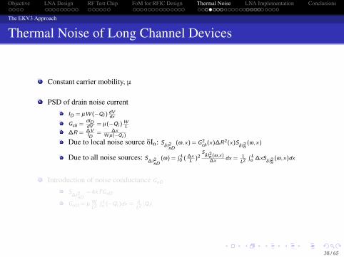

Objective LNA Design RF Test Chip FoM for RFIC Design Thermal Noise LNA Implementation Conclusions
The EKV3 Approach
Short Channel Effects
Velocity Saturation (VS) and Carrier Heating (CH)
Electrons and holes have a characteristic Ec and usat
When Ex becomes comparable to Ec then udrift startsto saturate
High lateral electric field
Carriers gain higher energyRandom collisions w. latticeCarrier temperature increases w. electric field
VS and CH, interdependent phenomena
EKV3 accounts for both
Critical field parameter
λc =2UTLeff Ec
The higher the λc , the stronger the SCE
Channel Length Modulation (CLM)
In S.I. as VDS increases the channel pinches off
Channel is split into two regions
Non-saturated region (Leff )VS region,ΔL
Carriers in VS region
Maximum velocityNoise voltage fluctuations do not propagateto drain
Only the active region contributes to channel thermalnoise
39 / 65
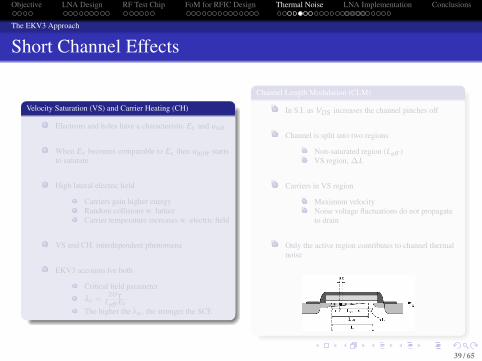

Objective LNA Design RF Test Chip FoM for RFIC Design Thermal Noise LNA Implementation Conclusions
The EKV3 Approach
Thermal Noise of Short Channel Devices
Incorporating SCE in PSD of drain noise current (Roy and Enz, TED 2005)
S.I. assumption (SCE dominant)Two transistor approachEffective mobility µeff varies w. Ex
Thermal noise conductance
GnD = M WL2eff
∫ Leff0 µz
TCTL
(−Qi(x))dx
Leff =L, for VD<VDsatL−∆L, for VD≥VDsat
VDeff =VD , for VD<VDsatVDsat , for VD≥VDsat
M = 1(1− VDeff −VS
2Leff EC)2
Analytical expression
40 / 65

Objective LNA Design RF Test Chip FoM for RFIC Design Thermal Noise LNA Implementation Conclusions
The EKV3 Approach
Thermal Noise Parameters
Thermal noise parameter: δ = GnDGds0
GnD and Gds0 calculated at different operating pointsLess relevant for circuit design
Thermal noise excess factor: γ = GnDGm
GnD and Gm calculated at the same operating pointsCharacterizes noise performance of transconductors
Used in noise calculation of cascode LNA: Fmin = 1 + 2γω
ωT
√βGγ
(1−c)2
The smaller γ, the better the noise performanceDramatically increases in linear operation
Importance of γ underestimated by scientific community
Not validated w. measurementsδ instead of γ
41 / 65

Objective LNA Design RF Test Chip FoM for RFIC Design Thermal Noise LNA Implementation Conclusions
Two-Port Noise Theory
Noise in Two-Port
Noise generated by any two-port device
Noiseless network w. two partially correlatednoise sources4 noise parameters
F = Fmin + RnGs|Ys −Yopt |2
Minimum noise figure, FminNoise resistance, RnOptimum source reflection coefficient, ΓoptYopt = Y0
1−Γopt1+Γopt
Noise matching when
GS = Gopt and BS = Bopt
42 / 65
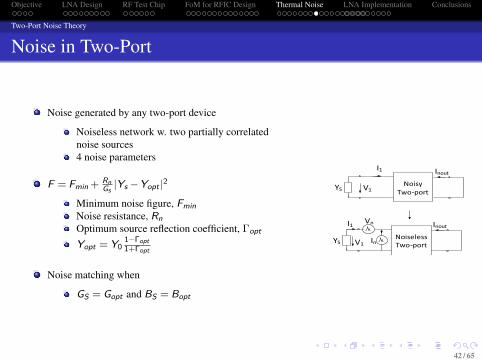

Objective LNA Design RF Test Chip FoM for RFIC Design Thermal Noise LNA Implementation Conclusions
Results and Discussion
HF Noise Parameters vs. Frequency
NMOS (L = 100nm,W = 40x2um, VGS = 0.65V ,VDS = 1.2V )
8 10 12 14 16 18 200
1
2
3
NF
min
(d
B)
Frequency (GHz)8 10 12 14 16 18 20
0
1
2
Rn
/50 (
−)
8 10 12 14 16 18 200
0.5
1
1.5
Frequency (GHz)
Γo
pt (
−)
real(Γopt
)
imag(Γopt
)
NMOS (L = 240nm,W = 40x2um, VGS = 0.65V ,VDS = 1.2V )
8 10 12 14 16 18 200
1
2
3
4
NF
min
(d
B)
Frequency (GHz)8 10 12 14 16 18 20
0
1
2
Rn
/50 (
−)
8 10 12 14 16 18 20
0
0.2
0.4
0.6
0.8
1
Frequency (GHz)
Γo
pt (
−)
real(Γopt
)
imag(Γopt
)
43 / 65

Objective LNA Design RF Test Chip FoM for RFIC Design Thermal Noise LNA Implementation Conclusions
Results and Discussion
HF Noise Parameters vs. Frequency
PMOS (L = 100nm,W = 40x2um, VGS =−0.65V ,VDS =−1.2V )
8 10 12 14 16 18 200
1
2
3
4
NF
min
(d
B)
Frequency (GHz)8 10 12 14 16 18 20
0
1
2
Rn
/50 (
−)
8 10 12 14 16 18 200
0.5
1
1.5
Frequency (GHz)
Γo
pt (
−)
real(Γopt
)
imag(Γopt
)
PMOS (L = 240nm,W = 40x2um, VGS =−0.65V ,VDS =−1.2V )
8 10 12 14 16 18 200
1
2
3
4
5
NF
min
(d
B)
Frequency (GHz)8 10 12 14 16 18 20
0
1
2
Rn
/50 (
−)
8 10 12 14 16 18 200
0.2
0.4
0.6
0.8
1
Frequency (GHz)
Γo
pt (
−)
real(Γopt
)
imag(Γopt
)
44 / 65
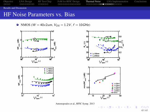
Objective LNA Design RF Test Chip FoM for RFIC Design Thermal Noise LNA Implementation Conclusions
Results and Discussion
HF Noise Parameters vs. Bias
NMOS (W = 40x2um, VDS = 1.2V , f = 10GHz)
100
101
102
0
1
2
3
NF
min
(d
B)
ID
/Ispec
(−)10
010
110
21e−1
1e0
1e1
1e2
Gass (
dB
)
100
101
102
20
30
40
50
60
70
Rn (
Ω)
ID
/Ispec
(−)
L=100nm
L=240nm
100
101
1020
0.2
0.4
0.6
0.8
1
|Γo
pt|
(−)
100
101
102
0
1
2
3
NF
min
(d
B)
ID
/Ispec
(−)
L=100nm
L=180nm
L=240nm
10 20 30 600
0.5
1
1.5
2
ID
/Ispec
(−)
min
(NF
min
) (d
B)
L=100nm
L=120nm
L=150nm
L=180nm
L=240nm
EKV3
Antonopoulos et al., RFIC Symp. 2013
45 / 65

Objective LNA Design RF Test Chip FoM for RFIC Design Thermal Noise LNA Implementation Conclusions
Results and Discussion
PSD of Drain Noise Current
NMOS and PMOS(W = 40x2um, |VDS |= 1.2V )
8 10 12 14 16 18 20
10−21
10−20
Frequency (GHz)
Sid
(A
2/H
z)
NMOS 240 nm
NMOS 180 nm
NMOS 150 nm
NMOS 120 nm
NMOS 100 nm
8 10 12 14 16 18 20
10−22
10−21
Frequency (GHz)
Sid
(A
2/H
z)
PMOS 240 nm
PMOS 180 nm
PMOS 120 nm
PMOS 100 nm
100
101
102
10−23
10−22
10−21
10−20
ID
/Ispec
(−)
Sid
(A
2/H
z)
NMOS 240 nm
NMOS 180 nm
NMOS 150 nm
NMOS 120 nm
NMOS 100 nm
PMOS 120nm
PMOS 100nm
Antonopoulos et al., IJNM 2014
46 / 65

Objective LNA Design RF Test Chip FoM for RFIC Design Thermal Noise LNA Implementation Conclusions
Results and Discussion
PSD of Drain Noise Current
NMOS (W = 40x2um, VDS = 1.2V , f = 10GHz)
0.5 0.6 0.7 0.8 0.9 1
10−21
10−20
VGS
(V)
Sid
(A
2/H
z)
100nm meas.
100nm model w. SCEs
100nm model wo.SCEs
180nm meas.
180nm model w. SCEs
180nm model wo. SCEs
100 120 180 240
10−21
10−20
Channel Length (nm)
Sid
(A
2/H
z)
VGS
=0.5V
VGS
=0.65V
VGS
=0.8V
VGS
=1V
Antonopoulos et al., TED 2013
47 / 65

Objective LNA Design RF Test Chip FoM for RFIC Design Thermal Noise LNA Implementation Conclusions
Results and Discussion
Design Parameters
NMOS (W = 40x2um, VDS = 1.2V , f = 10GHz)
0 5 10 15 200
1
2
3
4
vp=(V
G−V
To)/(n*U
T) (−)
Th
erm
al
No
ise
Ex
ce
ss
Fa
cto
r, γ
(−
)
100nm meas.
120nm meas.
180nm meas.
240nm meas.
Model w. SCEs
100
101
102
0
1
2
3
4
ID
/Ispec
(−)
Th
erm
al
No
ise
Ex
ce
ss
Fa
cto
r, γ
(−
)
100nm meas.
100nm model wo. SCEs
120nm meas.
120nm model wo. SCEs
180nm meas.
180nm model wo. SCEs
240nm meas.
240nm model wo. SCEs
model w. SCEs
100 120 180 240
1
2
3
4
5
Channel Length (nm)Th
erm
al N
ois
e E
xcess F
acto
r, γ
(−
)
VGS
=1V
VGS
=0.8V
VGS
=0.65V
VGS
=0.5V
100 120 180 240
0.6
0.8
1
1.2
1.4
1.6
1.8
Channel Length (nm)Th
erm
al
No
ise
P
ara
me
ter,
δ (
−)
δ=2/3
VGS
=1V
Model (VGS
=1V)
VGS
=0.65V
Model (VGS
=0.65V)
[23]
[24]
[18]
[4]
Antonopoulos et al., TED 2013
48 / 65

Objective LNA Design RF Test Chip FoM for RFIC Design Thermal Noise LNA Implementation Conclusions
Results and Discussion
Thermal Noise Parameter, δ
40 50 100 200 500 1000 20000
0.671
2
3
4
5
6
7
8
Channel length (nm)
Th
erm
al N
ois
e P
ara
mete
r, δ
(−
)
Patalay_2009_Gate_Length_VGS0.8_VDS1.1
Han_2003_VDS1.8
This_work_2013_VDS1.2
Smit_2014_Gate_Length_VGS1_VDS1.2
Chen_2002_VDS1.5
Scholten_2003_VDS1.8_VGS1.0
Ou_1999_VDS2
Triantis_1996_VGS0.5
Abidi_1986_VDS4
Jindal_1985
VGS=0.72VVDS=5V
VGS=0.6V
VGS=1.8V
VGS=0.65VVGS=1V
VGS=0.72VVDS=2V
VGS=0.97VVDS=3V
VGS=0.97VVDS=0.5V
VGS=1.1VVDS=0.5V
VGS=1.1VVDS=3V
VGS=1.2VVDS=3V
VGS=1.2VVDS=0.5V
VDS=2V
VDS=5V
VGS=1V
VGS=2V
VGS=3V
VGS=4V
VGS=5V
VGS=2V
VGS=0.9V
49 / 65

Objective LNA Design RF Test Chip FoM for RFIC Design Thermal Noise LNA Implementation Conclusions
Results and Discussion
Gate Current Noise
NMOS (W = 40x2um, VDS = 1.2V )
Correlation factor: c =Sigid∗√SigSid
8 10 2410
−24
10−23
10−22
Frequency (GHz)
Sig
(A
2/H
z)
Sig
∝ f2
L=100nm
L=180nm
0.5 0.6 0.7 0.8 0.910
−24
10−23
10−22
VGS
(V)
Sig
(A
2/H
z)
L=100nm
L=180nm
8 10 12 14 16 18 200
0.2
0.4
0.6
0.8
1
Frequency (GHz)
Im
ag
(c)
(−
)
Antonopoulos et al., TED 2013
50 / 65

Objective LNA Design RF Test Chip FoM for RFIC Design Thermal Noise LNA Implementation Conclusions
Contribution
Conclusions on High Frequency Noise
Detailed investigation of RF noise in MOSFETs in the context of circuit design
Frequency, L, and bias
Thermal noise excess factor measurements for the first time
SCE on thermal noise and γ
VS, CH, CLM
Optimum noise performance
Vicinity of S.I. to M.I.
Contribution
Thermal noise excess factor measurement and modeling for the first time
Minimum noise expected to shift to even lower inversion levels with more advancedtechnologies
51 / 65

Objective LNA Design RF Test Chip FoM for RFIC Design Thermal Noise LNA Implementation Conclusions
30 GHz LNA
30 GHz LNA Design
SNIM technique
Use minimum L to achieve high fT
Calculate Cgs and W from Zopt = Real(ZS)
Gopt = αωCgs√
δ
5γ(1−|c|2)
Calculate LS from a given power constraint from Real(Zin) = Real(ZS)
Real(Zin) = gmLSCgs
Calculate LG from Imag(Zin) = 0
Imag(Zin) = ω(LG +LS)− 1ωCgs −
1ωCpad
Optimum bias voltage by plotting fT vs. VOD
VGS = 0.65V
Output inductance resonates with output capacitance at 30 GHz
52 / 65
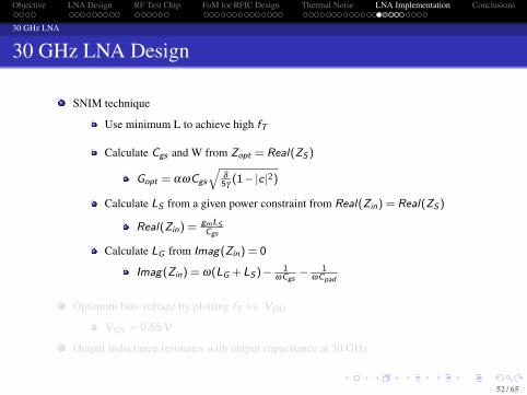

Objective LNA Design RF Test Chip FoM for RFIC Design Thermal Noise LNA Implementation Conclusions
30 GHz LNA
30 GHz LNA Layout
Uppermost metal (M9) for interconnect lines
Same orientation for all components
Interaction between transmission lines andinductors should be avoided
Width of interconnect lines determined by thecurrent they have to drive
Pad’s capacitance as low as possible
0.3762 mm2
53 / 65
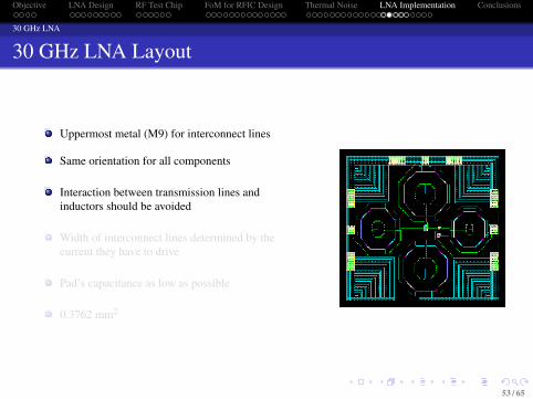

Objective LNA Design RF Test Chip FoM for RFIC Design Thermal Noise LNA Implementation Conclusions
30 GHz LNA
30 GHz LNA S-Parameters
20 25 30 35 40−30
−25
−20
−15
−10
−5
0
Frequency (GHz)
S11 (
dB
)
Pre−layout
Post−layout
20 25 30 35 40−50
−40
−30
−20
−10
Frequency (GHz)
S12 (
dB
)
Pre−layout
Post−layout
20 25 30 35 40−10
−5
0
5
10
Frequency (GHz)
S21 (
dB
)
Pre−layout
Post−layout
20 25 30 35 40−20
−15
−10
−5
0
Frequency (GHz)
S22 (
dB
)
Pre−layout
Post−layout
54 / 65

Objective LNA Design RF Test Chip FoM for RFIC Design Thermal Noise LNA Implementation Conclusions
30 GHz LNA
30 GHz LNA Noise, Stability, Linearity
20 25 30 35 403
3.5
4
4.5
5
5.5
Frequency (GHz)
NF
(d
B)
Pre−layout
Post−layout
20 25 30 35 40
1
5
10
Kf (
−)
Frequency (GHz)20 25 30 35 40
0
1
B1f (
−)
−40 −30 −20 −10 0 10−40
−30
−20
−10
0
10
20
Pin
(dBm)
Po
ut (
dB
m)
−40 −30 −20 −10 0 10−140
−100
−60
−20
20
Pin
(dBm)
Po
ut (
dB
m)
1st
order
3rd
order
55 / 65

Objective LNA Design RF Test Chip FoM for RFIC Design Thermal Noise LNA Implementation Conclusions
30 GHz LNA
30 GHz Single-Stage LNA Overall FoM
FoM = Gain(dB)·IIP3(mW )·fc (GHz)(NF−1)(abs)·PDC (mW )
This work
ICCDCS 2012
Abadi et al.
RFIC 2007
Yu et al.
MWCL 2004
Ribeiro et al.
EUROCON 2011
Sanduleanu et al.
RFIC 2006
Process (nm) 90 90 180 130 90
Freq. (GHz) 28.9 28.5 25.7 30 32.5
S21 (dB) 5.9 20 8.9 7.4 18.6
NF (dB) 3.9 2.9 6.9 3.7 3
IIP3 (dB) 4.9 -7.5 2.8 6 -
PDC (mW) 7.2 16.2 54 7 10
Area (mm2) 0.37 0.67 0.73 0.17* 0.85
FoM (-) 25.3 3.3 1.4 45.8 -
56 / 65

Objective LNA Design RF Test Chip FoM for RFIC Design Thermal Noise LNA Implementation Conclusions
5 GHz LNA
5 GHz WiMAX LNA Design
System level analysis of WiMAX RX
NF = 3dB, Gain = 18dB (could be relaxed)
Operation at 5.3GHz
Based on cascode topology (Andreani et al., CAS2 2001)
Extracted EKV3 model rather than the commercial one
Bias in M.I. region via (Gm/ID) · fTID = 1.47mAIC close to the center of M.I.
57 / 65
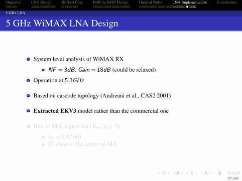

Objective LNA Design RF Test Chip FoM for RFIC Design Thermal Noise LNA Implementation Conclusions
5 GHz LNA
5 GHz WiMAX LNA Results
2 3 4 5 6 7 8
−80
−60
−40
−20
0
20
Frequency (GHz)
(dB
)
S11
S12
S21
S22
2 3 4 5 6 7 80
1
2
3
4
5
6
Frequency (GHz)
NF
(d
B)
NFNF
min
2 3 4 5 6 7 80
1
2
4
6
8
Frequency (GHz)
Sta
bilit
y C
oeff
icie
nts
(−
)
Kf
B1f
−40 −30 −20 −10 0−30
−20
−10
0
10
Pin
(dBm)
Po
ut (
dB
m)
58 / 65

Objective LNA Design RF Test Chip FoM for RFIC Design Thermal Noise LNA Implementation Conclusions
5 GHz LNA
5 GHz WiMAX LNA Overall FoM
High overall performance (FoM =Gain (dB)·IIP3(mW )·fc (GHz)
(NF−1)(abs)·PDC (mW ))
0
1
2
3
4
5
6
7
References
Fo
M (
−)
19.31 mW
3.96 mW
6.2 mW
2.6 mW
1.67 mW
10 mW
Lorenzo et al., ICCMS 2010
Asgaran et al., MWCL 2006
Allstot et al., RFIC Symp 2004
Liu et al., MOTL 2005
This work
Chiu et al., MTT 2005
59 / 65

Objective LNA Design RF Test Chip FoM for RFIC Design Thermal Noise LNA Implementation Conclusions
5 GHz LNA
Conclusions on LNA Design
Device to circuit via (Gm/ID) · fT FoM
Fairly high overall performance
Low power consumption
M.I. ideal for LNA design
60 / 65

Objective LNA Design RF Test Chip FoM for RFIC Design Thermal Noise LNA Implementation Conclusions
5 GHz LNA
Conclusions on LNA Design
Device to circuit via (Gm/ID) · fT FoM
Fairly high overall performance
Low power consumption
M.I. ideal for LNA design
60 / 65

Objective LNA Design RF Test Chip FoM for RFIC Design Thermal Noise LNA Implementation Conclusions
5 GHz LNA
Conclusions on LNA Design
Device to circuit via (Gm/ID) · fT FoM
Fairly high overall performance
Low power consumption
M.I. ideal for LNA design
60 / 65

Objective LNA Design RF Test Chip FoM for RFIC Design Thermal Noise LNA Implementation Conclusions
5 GHz LNA
Conclusions on LNA Design
Device to circuit via (Gm/ID) · fT FoM
Fairly high overall performance
Low power consumption
M.I. ideal for LNA design
60 / 65

Objective LNA Design RF Test Chip FoM for RFIC Design Thermal Noise LNA Implementation Conclusions
5 GHz LNA
Conclusions on LNA Design
Device to circuit via (Gm/ID) · fT FoM
Fairly high overall performance
Low power consumption
M.I. ideal for LNA design
60 / 65

Objective LNA Design RF Test Chip FoM for RFIC Design Thermal Noise LNA Implementation Conclusions
Final Conclusions
Low-power RF CMOS transceiver design
Connection between device and circuit performance
Design, layout and fabrication of an RF Test Chip w. a 30 GHz LNAFoM representative for LNA design vs. technology nodes, channel length and biasGreat potential of CMOS downscaling in realizing high performance low-power RFICs
Validation through the design of a WiMAX LNA at 5.3 GHz
Operation in M.I.(Gm/ID ) · fT as a design guideHigh overall performance w. minimum power consumption
RF noise characteristics vs.channel length scaling and IC
Excess noise factor
Importance in terms of RFIC design highlightedVerified w. measurements for the first timeImpact of SCE
Small-signal and noise results validated w. EKV3
61 / 65
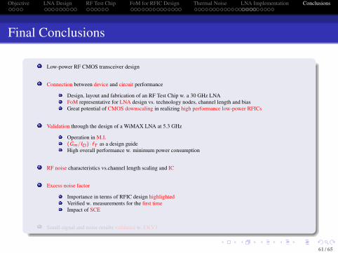

Objective LNA Design RF Test Chip FoM for RFIC Design Thermal Noise LNA Implementation Conclusions
Journal Publications
1 A. Antonopoulos, M. Bucher, K. Papathanasiou, N. Mavredakis, N. Makris, R. K. Sharma, P. Sakalas, M. Schroter,“CMOS Small-Signal and Thermal Noise Modeling at High Frequencies”, IEEE Trans. Electron Devices, Vol. 60, No.11, November 2013.
2 A. Antonopoulos, M. Bucher, K. Papathanasiou, N. Makris, N. Mavredakis, R. K. Sharma, P. Sakalas, M. Schroter,“Modeling of High Frequency Noise of Silicon MOS Transistors for RFIC Design”, International Journal ofNumerical Modelling: Electronic Networks, Devices and Fields, special issue on Modeling of high-frequency silicontransistors, in press.
3 W. Grabinski, M. Brinson, P. Nenzi, F. Lannutti, N. Makris, A. Antonopoulos, M. Bucher, “Open source circuitsimulation tools for RF compact semiconductor device modelling”, International Journal of Numerical Modelling:Electronic Networks, Devices and Fields, special issue on Modeling of high-frequency silicon transistors, invitedpaper, in press.
62 / 65

Objective LNA Design RF Test Chip FoM for RFIC Design Thermal Noise LNA Implementation Conclusions
Conference Publications
1 A. Antonopoulos, M. Bucher, K. Papathanasiou, N. Makris, R. K. Sharma, P. Sakalas, M. Schroter, “CMOS RF Noise,Scaling, and Compact Modeling for RFIC Design”, IEEE Radio Frequency Integrated Circuits Symposium (RFIC), pp.53-56, Seattle, June 2013.
2 R.K Sharma, A. Antonopoulos, N. Mavredakis, M. Bucher, “Impact of Design Engineering on RF Linearity and NoisePerformance of Nanoscale DG SOI MOSFETs”, 14th International Conference on Ultime Integration on Silicon(ULIS), pp. 145-148, Coventry, 2013.
3 A. Antonopoulos, K. Papathanasiou, M. Bucher, K. Papathanasiou, “CMOS LNA Design at 30 GHz – A Case Study”,8th International Caribbean Conference on Devices Circuits and Systems (ICCDCS), pp. 1-4, Playa Del Carmen, 2012.
4 R. K. Sharma, A. Antonopoulos, N. Mavredakis, M. Bucher, “Analog/RF Figures of Merit of Advanced DGMOSFETs”, 8th International Caribbean Conference on Devices Circuits and Systems (ICCDCS), pp. 1-4, Playa DelCarmen, 2012.
5 K. Papathanasiou, N. Makris, A. Antonopoulos, M. Bucher, “Moderate inversion: analog and RF benchmarking of theEKV3 compact model”, 29th International Conference on Microelectronics (MIEL), Belgrade, May 12-14, 2014,accepted.
63 / 65

Objective LNA Design RF Test Chip FoM for RFIC Design Thermal Noise LNA Implementation Conclusions
Acknowledgements
H παρούσvα έρευνα έχει σvυγχρηματοδοτηθεί από τηνΕυρωπαϊκή ΄Ενωσvη (ΕυρωπαϊκόΚοινωνικόΤαμείο- ΕΚΤ) και από εθνικούς πόρους μέσvω του Επιχειρησvιακού Προγράμματος «Εκπαίδευσvη και ΔιαΒίουΜάθησvη» τουΕθνικούΣτρατηγικούΠλαισvίουΑναφοράς (ΕΣΠΑ) –ΕρευνητικόΧρηματοδοτού-μενο ΄Εργο: Ηράκλειτος ΙΙ .Επένδυσvη σvτην κοινωνία της γνώσvης μέσvω του ΕυρωπαϊκούΚοινωνικούΤαμείου.
64 / 65

Objective LNA Design RF Test Chip FoM for RFIC Design Thermal Noise LNA Implementation Conclusions
Thank you for your attention!
65 / 65