Nanocrystalline cellulose applied simultaneously as the gate ...
11
Nanotechnology Nanotechnology 25 (2014) 094008 (11pp) doi:10.1088/0957-4484/25/9/094008 Nanocrystalline cellulose applied simultaneously as the gate dielectric and the substrate in flexible field effect transistors D Gaspar, S N Fernandes, A G de Oliveira, J G Fernandes, P Grey, R V Pontes, L Pereira, R Martins, M H Godinho and E Fortunato CENIMAT/I3N, Departamento de Ciência dos Materiais, Faculdade de Ciências e Tecnologia, Universidade Nova de Lisboa, Campus de Caparica, 2829-516 Caparica, Portugal E-mail: [email protected], [email protected] and [email protected] Received 2 August 2013, revised 10 October 2013 Published 12 February 2014 Abstract Cotton-based nanocrystalline cellulose (NCC), also known as nanopaper, one of the major sources of renewable materials, is a promising substrate and component for producing low cost fully recyclable flexible paper electronic devices and systems due to its properties (lightweight, stiffness, non-toxicity, transparency, low thermal expansion, gas impermeability and improved mechanical properties). Here, we have demonstrated for the first time a thin transparent nanopaper-based field effect transistor (FET) where NCC is simultaneously used as the substrate and as the gate dielectric layer in an ‘interstrate’ structure, since the device is built on both sides of the NCC films; while the active channel layer is based on oxide amorphous semiconductors, the gate electrode is based on a transparent conductive oxide. Such hybrid FETs present excellent operating characteristics such as high channel saturation mobility (>7 cm 2 V -1 s -1 ), drain–source current on/off modulation ratio higher than 10 5 , enhancement n-type operation and subthreshold gate voltage swing of 2.11 V/decade. The NCC film FET characteristics have been measured in air ambient conditions and present good stability, after two weeks of being processed, without any type of encapsulation or passivation layer. The results obtained are comparable to ones produced for conventional cellulose paper, marking this out as a promising approach for attaining high-performance disposable electronics such as paper displays, smart labels, smart packaging, RFID (radio-frequency identification) and point-of-care systems for self-analysis in bioscience applications, among others. Keywords: nanopaper, paper electronics, paper transistor, nanocellulose (Some figures may appear in colour only in the online journal) 1. Introduction Today’s electronics are manufactured with expensive materials associated with polluting technologies and without the possi- bility of being recyclable. On the other hand, cellulose paper is one of the most common and cheapest of all substrate materials used in our society, and is recyclable and biocompatible; however its application window is currently limited to being a carrier of printed information and packaging. Cellulose is the Earth’s major biopolymer and of tremendous global economic importance, especially in Europe, representing 30% of the world’s total production. Nevertheless the use of paper 0957-4484/14/094008+11$33.00 1 c 2014 IOP Publishing Ltd Printed in the UK
Transcript of Nanocrystalline cellulose applied simultaneously as the gate ...
Nanotechnology
Nanotechnology 25 (2014) 094008 (11pp) doi:10.1088/0957-4484/25/9/094008
Nanocrystalline cellulose appliedsimultaneously as the gate dielectricand the substrate in flexible field effecttransistorsD Gaspar, S N Fernandes, A G de Oliveira, J G Fernandes, P Grey,R V Pontes, L Pereira, R Martins, M H Godinho and E Fortunato
CENIMAT/I3N, Departamento de Ciência dos Materiais, Faculdade de Ciências e Tecnologia,Universidade Nova de Lisboa, Campus de Caparica, 2829-516 Caparica, Portugal
E-mail: [email protected], [email protected] and [email protected]
Received 2 August 2013, revised 10 October 2013Published 12 February 2014
AbstractCotton-based nanocrystalline cellulose (NCC), also known as nanopaper, one of the majorsources of renewable materials, is a promising substrate and component for producing lowcost fully recyclable flexible paper electronic devices and systems due to its properties(lightweight, stiffness, non-toxicity, transparency, low thermal expansion, gas impermeabilityand improved mechanical properties).
Here, we have demonstrated for the first time a thin transparent nanopaper-based fieldeffect transistor (FET) where NCC is simultaneously used as the substrate and as the gatedielectric layer in an ‘interstrate’ structure, since the device is built on both sides of the NCCfilms; while the active channel layer is based on oxide amorphous semiconductors, the gateelectrode is based on a transparent conductive oxide.
Such hybrid FETs present excellent operating characteristics such as high channelsaturation mobility (>7 cm2 V−1 s−1), drain–source current on/off modulation ratio higherthan 105, enhancement n-type operation and subthreshold gate voltage swing of2.11 V/decade. The NCC film FET characteristics have been measured in air ambientconditions and present good stability, after two weeks of being processed, without any type ofencapsulation or passivation layer. The results obtained are comparable to ones produced forconventional cellulose paper, marking this out as a promising approach for attaininghigh-performance disposable electronics such as paper displays, smart labels, smartpackaging, RFID (radio-frequency identification) and point-of-care systems for self-analysisin bioscience applications, among others.
Keywords: nanopaper, paper electronics, paper transistor, nanocellulose
(Some figures may appear in colour only in the online journal)
1. Introduction
Today’s electronics are manufactured with expensive materialsassociated with polluting technologies and without the possi-bility of being recyclable. On the other hand, cellulose paper isone of the most common and cheapest of all substrate materials
used in our society, and is recyclable and biocompatible;however its application window is currently limited to beinga carrier of printed information and packaging. Celluloseis the Earth’s major biopolymer and of tremendous globaleconomic importance, especially in Europe, representing 30%of the world’s total production. Nevertheless the use of paper
0957-4484/14/094008+11$33.00 1 c© 2014 IOP Publishing Ltd Printed in the UK
Nanotechnology 25 (2014) 094008 D Gaspar et al
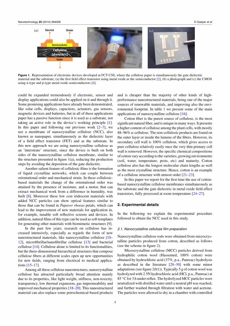
Figure 1. Representation of electronic devices developed at FCT-UNL where the cellulose paper is simultaneously the gate dielectricmaterial and the substrate; (a) the first field effect transistor using metal oxide as the semiconductor [2], (b) a photograph and (c) the CMOSusing n-type and p-type metal oxide semiconductors [4].
could be expanded tremendously if electronic, sensor anddisplay applications could also be applied on it and through it.Some promising applications have already been demonstrated,like solar cells, displays, capacitors, actuators, gas sensors,magnetic devices and batteries, but in all of these applicationspaper has a passive function since it is used as a substrate, nottaking an active role in the device’s working principle [1].In this paper and following our previous work [2–7], weuse a membrane of nanocrystalline cellulose (NCC), alsoknown as nanopaper, simultaneously as the dielectric layerof a field effect transistor (FET) and as the substrate. Inthis new approach we are using nanocrystalline cellulose asan ‘interstrate’ structure, since the device is built on bothsides of the nanocrystalline cellulose membrane, similar tothe structure presented in figure 1(a), reducing the productionsteps by avoiding the deposition of the gate dielectric.
Another salient feature of cellulosic films is the formationof liquid crystalline networks, which can couple betweenorientational order and mechanical strain. In these cellulosic-based materials the change of the orientational order wasattained by the presence of moisture, and a motor, that canextract mechanical work from a difference in humidity, wasbuilt [8]. Moreover these low cost iridescent materials withadded NCC particles can show optical features similar tothose that can be found in Papaver rhoeas petals, which canlead to the improvement of new materials for application in,for example, tunable soft reflective screens and devices. Inaddition, natural films of this type can be used as soft templatesfor generating other materials with biomimetic structures [9].
In the past few years, research on cellulose has in-creased intensively, especially as regards the form of newnanostructured materials, like nanocrystalline cellulose [10–12], microfibrillar/nanofibrillar cellulose [13] and bacterialcellulose [14]. Cellulose alone is limited to its functionalities,but the three-dimensional hierarchical structures that composecellulose fibers at different scales open up new opportunitiesfor new fields, ranging from electrical to medical applica-tions [15–17].
Among all these cellulose nanostructures, nanocrystallinecellulose has attracted particularly broad attention mainlydue to its properties, like light weight, stiffness, non-toxicity,transparency, low thermal expansion, gas impermeability andimproved mechanical properties [18–20]. This nanostructuredmaterial can also replace some petrochemical-based products
and is cheaper than the majority of other kinds of high-performance nanostructured materials, being one of the majorsources of renewable materials, and improving also the envi-ronmental footprint. In table 1 we present some of the mainapplications of nanocrystalline cellulose [16].
Cotton fiber is the purest source of cellulose, is the mostsignificant natural fiber, and is unique in many ways. It presentsa higher content of cellulose among the plant cells, with mostly88–96% α-cellulose. The non-cellulosic products are found onthe outer layer or inside the lumens of the fibers. However, itssecondary cell wall is 100% cellulose, which gives access topure cellulose relatively easily once the very thin primary cellwall is removed. However, the specific chemical compositionsof cotton vary according to the varieties, growing environments(soil, water, temperature, pests, etc) and maturity. Cottoncellulose also has the longest molecular chain lengths as wellas the most crystalline structure. Hence, cotton is an exampleof a cellulose structure with utmost order [21–23].
In this paper we report for the first time the use of cotton-based nanocrystalline cellulose membranes simultaneously asthe substrate and the gate dielectric in metal oxide field effecttransistors, fully processed at room temperature [24–27].
2. Experimental details
In the following we explain the experimental procedurefollowed to obtain the NCC used in this study.
2.1. Nanocrystalline cellulose film preparation
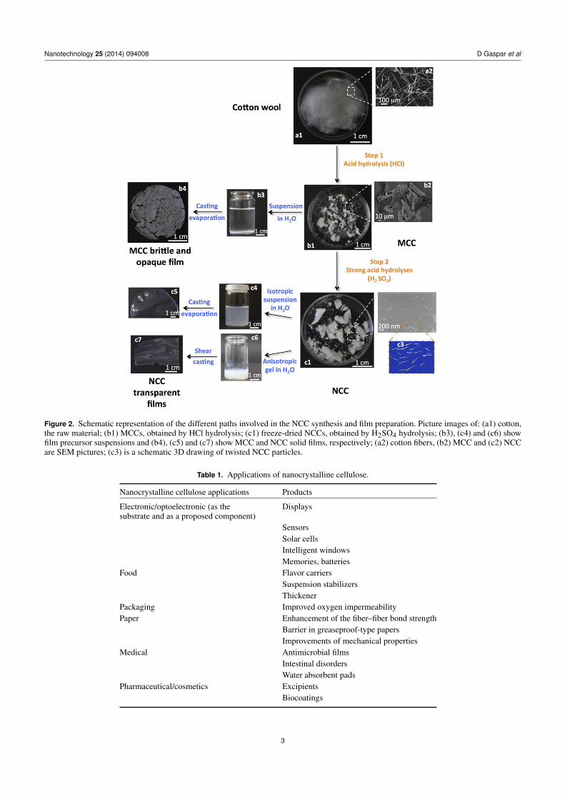
Nanocrystalline cellulose rods were obtained from microcrys-talline particles produced from cotton, described as follows(see the scheme in figure 2).
Microcrystalline cellulose (MCC) particles derived fromhydrophilic cotton wool (Hassemed, 100% cotton) wereobtained by hydrochloric acid (37%, p.a., Panreac) hydrolysisas described in the literature [28–30] with some minoradaptations (see figure 2(b1)). Typically 5 g of cotton wool washydrolyzed with 2.5N hydrochloric acid (HCl, p.a., Panreac) at85 ◦C for 3 h under reflux. The hydrolyzed MCC particles wereneutralized with distilled water until a neutral pH was reached,and further washed through filtration with water and acetone.The particles were allowed to dry in a chamber with controlled
2
Nanotechnology 25 (2014) 094008 D Gaspar et al
Figure 2. Schematic representation of the different paths involved in the NCC synthesis and film preparation. Picture images of: (a1) cotton,the raw material; (b1) MCCs, obtained by HCl hydrolysis; (c1) freeze-dried NCCs, obtained by H2SO4 hydrolysis; (b3), (c4) and (c6) showfilm precursor suspensions and (b4), (c5) and (c7) show MCC and NCC solid films, respectively; (a2) cotton fibers, (b2) MCC and (c2) NCCare SEM pictures; (c3) is a schematic 3D drawing of twisted NCC particles.
Table 1. Applications of nanocrystalline cellulose.
Nanocrystalline cellulose applications Products
Electronic/optoelectronic (as thesubstrate and as a proposed component)
Displays
SensorsSolar cellsIntelligent windowsMemories, batteries
Food Flavor carriersSuspension stabilizersThickener
Packaging Improved oxygen impermeabilityPaper Enhancement of the fiber–fiber bond strength
Barrier in greaseproof-type papersImprovements of mechanical properties
Medical Antimicrobial filmsIntestinal disordersWater absorbent pads
Pharmaceutical/cosmetics ExcipientsBiocoatings
3
Nanotechnology 25 (2014) 094008 D Gaspar et al
humidity (∼10%) until constant weight was obtained (∼85%yield).
The dimensions of the MCC are in the ranges of160–12 µm length and 25–2 µm diameter and were obtainedfrom the scanning electron microscopy (SEM) images of theparticles. The lengths and diameter of individual microparti-cles/nanoparticles visible in these images were measured withImageJ (version 1.45s, http://imagej.nih.gov/ij/) and scaledaccording to the magnification quoted by the microscopesoftware. A minimum of 50 length measurements were takenfor each sample.
Nanocrystalline cellulose particles were prepared on thebasis of the methods of Gray et al [11, 31] and Orts et al [32]with minor adaptations (see figure 2(c1)). Microcrystallinecellulose was hydrolyzed with sulfuric acid (97%, p.a., Merck)with an acid/solid ratio of 17.5 at 45 ◦C for 130 min undervigorous stirring. The resultant suspension was washed withultrapure water by successive dilution and centrifugation (at1200 rpm for 20 min) until the supernatant was turbid (thatoccurs at approximately pH 1.9–3.8). The resulting suspensionwas placed in a Spectra/Por 4 cellulose membrane (Spectrum)and dialyzed against ultrapure water until a pH of 6–7 wasreached. A suspension of 0.5–0.7% of NCC, determinedby gravimetry, was obtained. The content of NCC in thesuspension was increased by subsequent centrifugations (at14 500 rpm for 20 min) and a gel-type substance was obtained.The water used in these experiments was purified by using aMillipore Elix Advantage 3 purification system.
Solid films of microcrystalline cellulose were preparedby slow casting and evaporation of water from suspensionsof 1–5% MCC under ambient conditions in polystyrene Petridishes (90 mm diameter). The resulting films had a thicknessof approximately 60 µm, estimated from the average of tenmeasurements made using a Mitutoyo digital micrometer;however they are too brittle to undergo further treatment(figure 2(b4)).
Free-standing transparent NCC films were prepared bytwo different methods: solvent casting and evaporation, fur-ther designated only as evaporation (NCC E), and shearedcasting, further designated only as casting (NCC C). Solidfilms of the nanocrystalline cellulose were prepared by slowcasting and evaporation of water from 60 ml (0.3–0.7% NCCcontent; figure 2(c4)) of the NCC suspension under ambientconditions in polystyrene Petri dishes (90 mm diameter). Theresulting films had a thickness of approximately 30–55 µm(figure 2(c5)).
Films were also prepared from suspensions with 5–6%NCC content (figure 2(c6)), cast, and sheared simultaneouslyby moving a calibrated Gardner knife from Braive Instru-ments at 1.25 mm s−1 over a polystyrene sheet. The films,35–55 µm thick, were allowed to dry at room temperature(see figure 2(c7)).
2.2. Film characterization
Scanning electron microscopy (SEM) images of the nanocrys-talline cellulose films were acquired with a Carl Zeiss Aurigacrossbeam (SEM-FIB) workstation instrument equipped with
an Oxford energy dispersive x-ray spectrometer. The SEMimages were taken in the in-lens mode with an accelerationvoltage of 2 kV and aperture size of 30 µm. The nanocrys-talline cellulose films were glued on aluminum stubs using adouble-sided carbon tape and coated with a thin carbon layer(< 20 nm) using a Q300T D Quorum sputter coater.
The structural analysis of the samples was done viax-ray diffraction (XRD, PANalytical, model X’Pert Pro) inBragg–Brentano geometry with Cu Kα line radiation (λ =1.5406 Å) at 45 kV and 40 mA, the instrument being equippedwith an X’Celerator detector. The XRD patterns were collectedwith a scanning step of 0.0334◦ over the angular 2θ range10◦–40◦, with a total acquisition time of 4 min.
The crystallinity index (Ic) was determined using theempirical method proposed by Segal et al [33]:
Ic =I(002)− I(am)
I(002)× 100 (1)
where I(002) is the maximum intensity of diffraction of the(002) lattice peak at a 2θ angle between 21◦ and 23◦, whichrepresents the crystalline counterpart. I(am) is the intensityof diffraction of the amorphous material, which is taken ata 2θ angle between 18◦ and 20◦ where the intensity is at aminimum. It should be noted that the crystallinity index isonly valid as a comparison basis, as it is used to indicate theorder of crystallinity rather than the crystallinity of crystallineregions.
The crystallite size was inferred through the Scherrerequation [34]:
Dhkl =0.9λβ cos θ
(2)
where Dhkl is the crystallite size in the direction normal to thehkl lattice planes, λ is the x-ray radiation wavelength, β is thefull width at half-maximum (FWHM) of the diffraction peakand θ is the corresponding Bragg angle.
The diffractograms obtained were analyzed with specificsoftware (HighScore Plus) that allows the deconvolution ofKα1 and Kα2 cases. The data obtained from the XRDmeasurement are treated to obtain more accurate informationon peak parameters such as position, intensity, width andshape. Using the software, the background is determined,the peaks are searched (Kα1 and Kα2 not separated) andit is possible to fit the profile of the peaks, in which Kα1and Kα2 are deconvoluted. The peak profile characteristicsare calculated by applying adjustable, mathematical profilefunctions. The software also calculates the FWHM.
Thermogravimetric analysis measurements (TGA) werecarried out with a simultaneous thermal analyzer (TGA-DSC-STA 449 F3 Jupiter). Approximately 3 mg of each sample wasloaded into an aluminum pan and heated from 25 to 550 ◦Cwith a heating rate of 5 ◦C min−1. All the measurements wereperformed under air atmosphere.
Fourier transform infra-red (FTIR) spectroscopy datawere recorded using an attenuated total reflectance (ATR) sam-pling accessory (Smart iTR) equipped with a single-bouncediamond crystal on a Thermo Nicolet 6700 spectrometer. The
4
Nanotechnology 25 (2014) 094008 D Gaspar et al
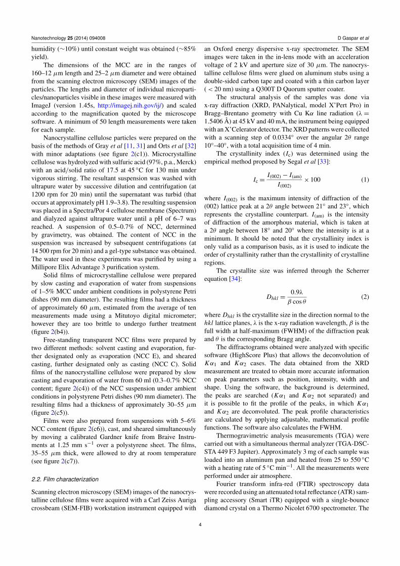
Figure 3. Schematics of the process of fabrication of FETs using NCC as the gate dielectric, and the corresponding staggered-bottom gatestructure used in this work.
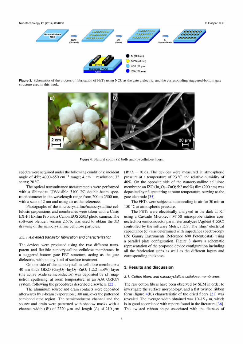
Figure 4. Natural cotton (a) bolls and (b) cellulose fibers.
spectra were acquired under the following conditions: incidentangle of 45◦; 4000–650 cm−1 range; 4 cm−1 resolution; 32scans; 20 ◦C.
The optical transmittance measurements were performedwith a Shimadzu UV/visible 3100 PC double-beam spec-trophotometer in the wavelength range from 200 to 2500 nm,with a scan of 2 nm and using air as the reference.
Photographs of the microcrystalline/nanocrystalline cel-lulosic suspensions and membranes were taken with a CasioEX-F1 Exilim Pro and a Canon EOS 550D photo camera. Thesoftware blender, version 2.57b, was used to obtain the 3Ddrawing of the nanocrystalline cellulose particles.
2.3. Field effect transistor fabrication and characterization
The devices were produced using the two different trans-parent and flexible nanocrystalline cellulose membranes ina staggered-bottom gate FET structure, acting as the gatedielectric, without any kind of surface treatment.
On one side of the nanocrystalline cellulose membrane a40 nm thick GIZO (Ga2O3–In2O3–ZnO; 1:2:2 mol%) layer(the active oxide semiconductor) was deposited by r.f. mag-netron sputtering, at room temperature, in an AJA ORIONsystem, following the procedures described elsewhere [22].
The aluminum source and drain contacts were depositedafterwards by e-beam evaporation (100 nm) over the patternedsemiconductor region. The semiconductor channel and thesource and drain were patterned with shadow masks with achannel width (W ) of 2220 µm and length (L) of 210 µm
(W/L = 10.6). The devices were measured at atmosphericpressure at a temperature of 23 ◦C and relative humidity of40%. On the opposite side of the nanocrystalline cellulosemembrane an IZO (In2O3–ZnO; 5:2 mol%) film (200 nm) wasdeposited by r.f. sputtering at room temperature, serving as thegate electrode [35].
The FETs were subjected to annealing in air for 30 min at150 ◦C at atmospheric pressure.
The FETs were electrically analyzed in the dark at RTusing a Cascade Microtech M150 microprobe station con-nected to a semiconductor parameter analyzer (Agilent 4155C)controlled by the software Metrics ICS. The films’ electricalcapacitance (C) was determined with impedance spectroscopy(IS; Gamry Instruments Reference 600 Potentiostat) usinga parallel plate configuration. Figure 3 shows a schematicrepresentation of the proposed device configuration includingall the fabrication steps as well as the different layers andcorresponding thickness.
3. Results and discussion
3.1. Cotton fibers and nanocrystalline cellulose membranes
The raw cotton fibers have been observed by SEM in order toinvestigate the surface morphology, and a flat twisted ribbonform (figure 4(b)) characteristic of the dried fibers [21] wasrevealed. The average width obtained was 10–15 µm, whichis in good accordance with reports found in the literature [36].This twisted ribbon shape associated with the flatness of
5
Nanotechnology 25 (2014) 094008 D Gaspar et al
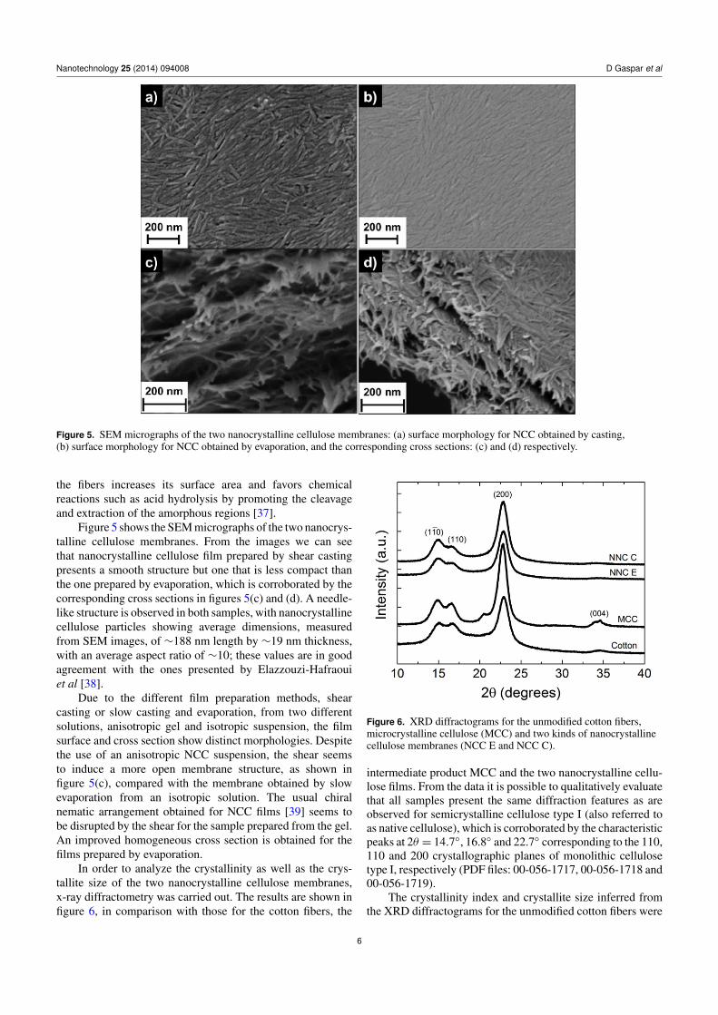
Figure 5. SEM micrographs of the two nanocrystalline cellulose membranes: (a) surface morphology for NCC obtained by casting,(b) surface morphology for NCC obtained by evaporation, and the corresponding cross sections: (c) and (d) respectively.
the fibers increases its surface area and favors chemicalreactions such as acid hydrolysis by promoting the cleavageand extraction of the amorphous regions [37].
Figure 5 shows the SEM micrographs of the two nanocrys-talline cellulose membranes. From the images we can seethat nanocrystalline cellulose film prepared by shear castingpresents a smooth structure but one that is less compact thanthe one prepared by evaporation, which is corroborated by thecorresponding cross sections in figures 5(c) and (d). A needle-like structure is observed in both samples, with nanocrystallinecellulose particles showing average dimensions, measuredfrom SEM images, of ∼188 nm length by ∼19 nm thickness,with an average aspect ratio of ∼10; these values are in goodagreement with the ones presented by Elazzouzi-Hafraouiet al [38].
Due to the different film preparation methods, shearcasting or slow casting and evaporation, from two differentsolutions, anisotropic gel and isotropic suspension, the filmsurface and cross section show distinct morphologies. Despitethe use of an anisotropic NCC suspension, the shear seemsto induce a more open membrane structure, as shown infigure 5(c), compared with the membrane obtained by slowevaporation from an isotropic solution. The usual chiralnematic arrangement obtained for NCC films [39] seems tobe disrupted by the shear for the sample prepared from the gel.An improved homogeneous cross section is obtained for thefilms prepared by evaporation.
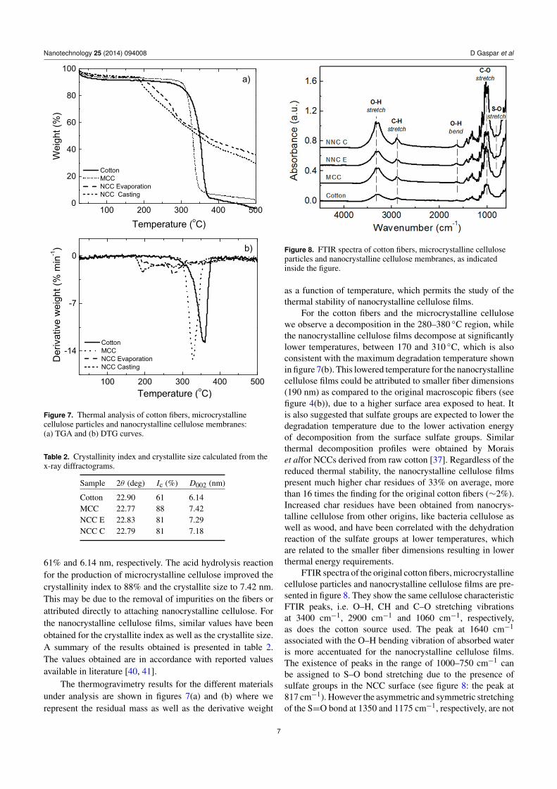
In order to analyze the crystallinity as well as the crys-tallite size of the two nanocrystalline cellulose membranes,x-ray diffractometry was carried out. The results are shown infigure 6, in comparison with those for the cotton fibers, the
Figure 6. XRD diffractograms for the unmodified cotton fibers,microcrystalline cellulose (MCC) and two kinds of nanocrystallinecellulose membranes (NCC E and NCC C).
intermediate product MCC and the two nanocrystalline cellu-lose films. From the data it is possible to qualitatively evaluatethat all samples present the same diffraction features as areobserved for semicrystalline cellulose type I (also referred toas native cellulose), which is corroborated by the characteristicpeaks at 2θ = 14.7◦, 16.8◦ and 22.7◦ corresponding to the 110,110 and 200 crystallographic planes of monolithic cellulosetype I, respectively (PDF files: 00-056-1717, 00-056-1718 and00-056-1719).
The crystallinity index and crystallite size inferred fromthe XRD diffractograms for the unmodified cotton fibers were
6
Nanotechnology 25 (2014) 094008 D Gaspar et al
Figure 7. Thermal analysis of cotton fibers, microcrystallinecellulose particles and nanocrystalline cellulose membranes:(a) TGA and (b) DTG curves.
Table 2. Crystallinity index and crystallite size calculated from thex-ray diffractograms.
Sample 2θ (deg) Ic (%) D002 (nm)
Cotton 22.90 61 6.14MCC 22.77 88 7.42NCC E 22.83 81 7.29NCC C 22.79 81 7.18
61% and 6.14 nm, respectively. The acid hydrolysis reactionfor the production of microcrystalline cellulose improved thecrystallinity index to 88% and the crystallite size to 7.42 nm.This may be due to the removal of impurities on the fibers orattributed directly to attaching nanocrystalline cellulose. Forthe nanocrystalline cellulose films, similar values have beenobtained for the crystallite index as well as the crystallite size.A summary of the results obtained is presented in table 2.The values obtained are in accordance with reported valuesavailable in literature [40, 41].
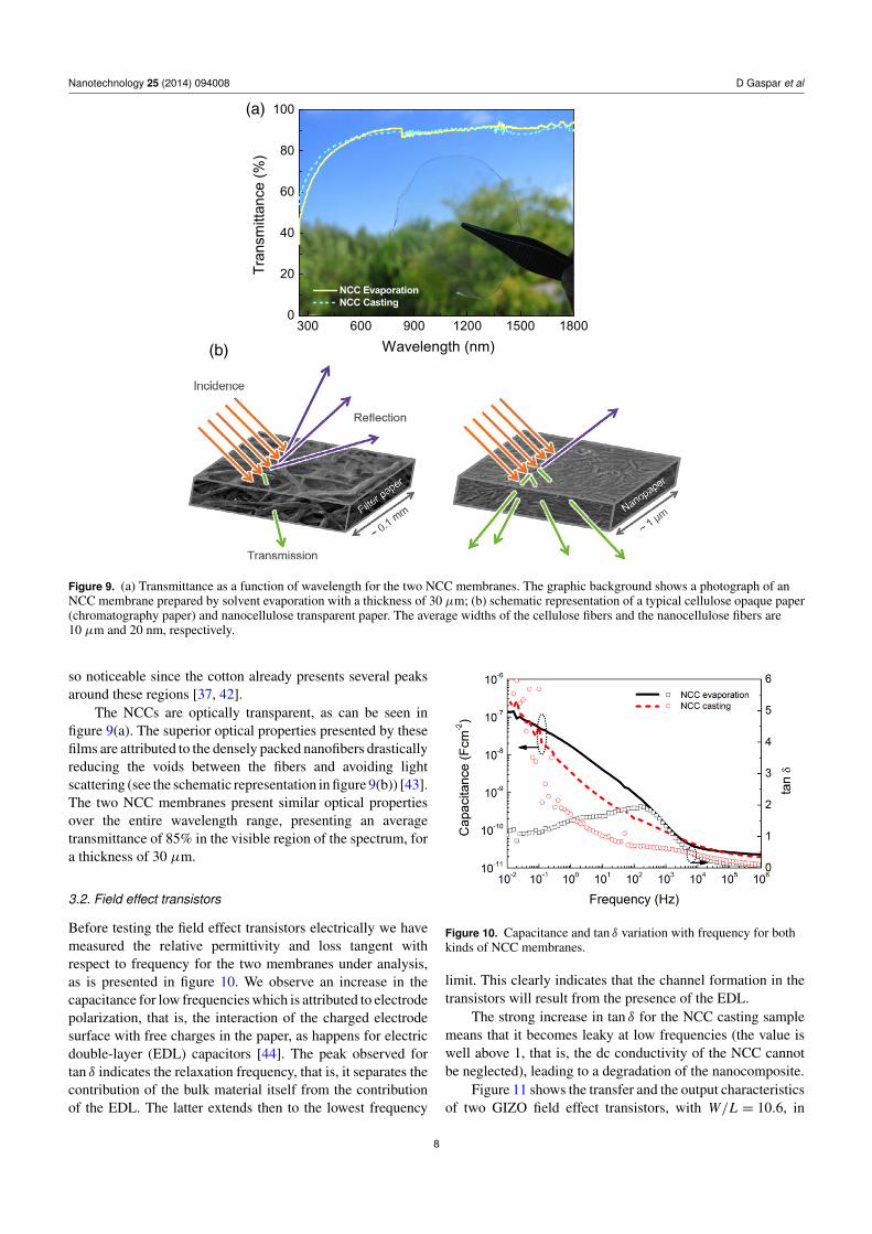
The thermogravimetry results for the different materialsunder analysis are shown in figures 7(a) and (b) where werepresent the residual mass as well as the derivative weight
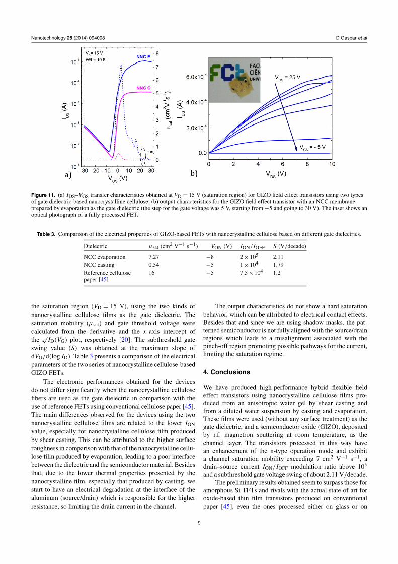
Figure 8. FTIR spectra of cotton fibers, microcrystalline celluloseparticles and nanocrystalline cellulose membranes, as indicatedinside the figure.
as a function of temperature, which permits the study of thethermal stability of nanocrystalline cellulose films.
For the cotton fibers and the microcrystalline cellulosewe observe a decomposition in the 280–380 ◦C region, whilethe nanocrystalline cellulose films decompose at significantlylower temperatures, between 170 and 310 ◦C, which is alsoconsistent with the maximum degradation temperature shownin figure 7(b). This lowered temperature for the nanocrystallinecellulose films could be attributed to smaller fiber dimensions(190 nm) as compared to the original macroscopic fibers (seefigure 4(b)), due to a higher surface area exposed to heat. Itis also suggested that sulfate groups are expected to lower thedegradation temperature due to the lower activation energyof decomposition from the surface sulfate groups. Similarthermal decomposition profiles were obtained by Moraiset alfor NCCs derived from raw cotton [37]. Regardless of thereduced thermal stability, the nanocrystalline cellulose filmspresent much higher char residues of 33% on average, morethan 16 times the finding for the original cotton fibers (∼2%).Increased char residues have been obtained from nanocrys-talline cellulose from other origins, like bacteria cellulose aswell as wood, and have been correlated with the dehydrationreaction of the sulfate groups at lower temperatures, whichare related to the smaller fiber dimensions resulting in lowerthermal energy requirements.
FTIR spectra of the original cotton fibers, microcrystallinecellulose particles and nanocrystalline cellulose films are pre-sented in figure 8. They show the same cellulose characteristicFTIR peaks, i.e. O–H, CH and C–O stretching vibrationsat 3400 cm−1, 2900 cm−1 and 1060 cm−1, respectively,as does the cotton source used. The peak at 1640 cm−1
associated with the O–H bending vibration of absorbed wateris more accentuated for the nanocrystalline cellulose films.The existence of peaks in the range of 1000–750 cm−1 canbe assigned to S–O bond stretching due to the presence ofsulfate groups in the NCC surface (see figure 8: the peak at817 cm−1). However the asymmetric and symmetric stretchingof the S=O bond at 1350 and 1175 cm−1, respectively, are not
7
Nanotechnology 25 (2014) 094008 D Gaspar et al
Figure 9. (a) Transmittance as a function of wavelength for the two NCC membranes. The graphic background shows a photograph of anNCC membrane prepared by solvent evaporation with a thickness of 30 µm; (b) schematic representation of a typical cellulose opaque paper(chromatography paper) and nanocellulose transparent paper. The average widths of the cellulose fibers and the nanocellulose fibers are10 µm and 20 nm, respectively.
so noticeable since the cotton already presents several peaksaround these regions [37, 42].
The NCCs are optically transparent, as can be seen infigure 9(a). The superior optical properties presented by thesefilms are attributed to the densely packed nanofibers drasticallyreducing the voids between the fibers and avoiding lightscattering (see the schematic representation in figure 9(b)) [43].The two NCC membranes present similar optical propertiesover the entire wavelength range, presenting an averagetransmittance of 85% in the visible region of the spectrum, fora thickness of 30 µm.
3.2. Field effect transistors
Before testing the field effect transistors electrically we havemeasured the relative permittivity and loss tangent withrespect to frequency for the two membranes under analysis,as is presented in figure 10. We observe an increase in thecapacitance for low frequencies which is attributed to electrodepolarization, that is, the interaction of the charged electrodesurface with free charges in the paper, as happens for electricdouble-layer (EDL) capacitors [44]. The peak observed fortan δ indicates the relaxation frequency, that is, it separates thecontribution of the bulk material itself from the contributionof the EDL. The latter extends then to the lowest frequency
Figure 10. Capacitance and tan δ variation with frequency for bothkinds of NCC membranes.
limit. This clearly indicates that the channel formation in thetransistors will result from the presence of the EDL.
The strong increase in tan δ for the NCC casting samplemeans that it becomes leaky at low frequencies (the value iswell above 1, that is, the dc conductivity of the NCC cannotbe neglected), leading to a degradation of the nanocomposite.
Figure 11 shows the transfer and the output characteristicsof two GIZO field effect transistors, with W/L = 10.6, in
8
Nanotechnology 25 (2014) 094008 D Gaspar et al
Figure 11. (a) IDS–VGS transfer characteristics obtained at VD = 15 V (saturation region) for GIZO field effect transistors using two typesof gate dielectric-based nanocrystalline cellulose; (b) output characteristics for the GIZO field effect transistor with an NCC membraneprepared by evaporation as the gate dielectric (the step for the gate voltage was 5 V, starting from −5 and going to 30 V). The inset shows anoptical photograph of a fully processed FET.
Table 3. Comparison of the electrical properties of GIZO-based FETs with nanocrystalline cellulose based on different gate dielectrics.
Dielectric µsat (cm2 V−1 s−1) VON (V) ION/IOFF S (V/decade)
NCC evaporation 7.27 −8 2× 10⁵ 2.11NCC casting 0.54 −5 1× 10⁴ 1.79Reference cellulosepaper [45]
16 −5 7.5× 10⁴ 1.2
the saturation region (VD = 15 V), using the two kinds ofnanocrystalline cellulose films as the gate dielectric. Thesaturation mobility (µsat) and gate threshold voltage werecalculated from the derivative and the x-axis intercept ofthe√
ID(VG) plot, respectively [20]. The subthreshold gateswing value (S) was obtained at the maximum slope ofdVG/d(log ID). Table 3 presents a comparison of the electricalparameters of the two series of nanocrystalline cellulose-basedGIZO FETs.
The electronic performances obtained for the devicesdo not differ significantly when the nanocrystalline cellulosefibers are used as the gate dielectric in comparison with theuse of reference FETs using conventional cellulose paper [45].The main differences observed for the devices using the twonanocrystalline cellulose films are related to the lower IONvalue, especially for nanocrystalline cellulose film producedby shear casting. This can be attributed to the higher surfaceroughness in comparison with that of the nanocrystalline cellu-lose film produced by evaporation, leading to a poor interfacebetween the dielectric and the semiconductor material. Besidesthat, due to the lower thermal properties presented by thenanocrystalline film, especially that produced by casting, westart to have an electrical degradation at the interface of thealuminum (source/drain) which is responsible for the higherresistance, so limiting the drain current in the channel.
The output characteristics do not show a hard saturationbehavior, which can be attributed to electrical contact effects.Besides that and since we are using shadow masks, the pat-terned semiconductor is not fully aligned with the source/drainregions which leads to a misalignment associated with thepinch-off region promoting possible pathways for the current,limiting the saturation regime.
4. Conclusions
We have produced high-performance hybrid flexible fieldeffect transistors using nanocrystalline cellulose films pro-duced from an anisotropic water gel by shear casting andfrom a diluted water suspension by casting and evaporation.These films were used (without any surface treatment) as thegate dielectric, and a semiconductor oxide (GIZO), depositedby r.f. magnetron sputtering at room temperature, as thechannel layer. The transistors processed in this way havean enhancement of the n-type operation mode and exhibita channel saturation mobility exceeding 7 cm2 V−1 s−1, adrain–source current ION/IOFF modulation ratio above 105
and a subthreshold gate voltage swing of about 2.11 V/decade.The preliminary results obtained seem to surpass those for
amorphous Si TFTs and rivals with the actual state of art foroxide-based thin film transistors produced on conventionalpaper [45], even the ones processed either on glass or on
9
Nanotechnology 25 (2014) 094008 D Gaspar et al
crystalline silicon substrates, processed or annealed at hightemperatures.
Transparent nanocrystalline cellulose films open up newperspectives for applications for cellulose devices. The com-patibility of these devices with large-scale/large-area depo-sition techniques and low cost substrates marks this out as apromising approach for attaining high-performance disposableelectronics like paper displays, smart labels, smart packaging,RFID and point-of-care systems for self-analysis in bioscienceapplications, among others.
We are watching the unfolding of one of the greatestopportunities for innovation in the forest products industry:the production and use of cellulose nanomaterials for a broadrange of applications.
Work is under way in efforts to understand the operatingmechanism of the device, in order to improve its stability overtime.
Acknowledgments
This work was financed by the European Commissionunder projects INVISIBLE (FP7 ERC AdG No. 228144),ORAMA CP-IP 246334-2, and APPLE (FP7-NMP-2010-SME/262782-2), and the Portuguese Science Foundation(FCT-MEC) through the Projects PEst-C/CTM/LA0025/2013-14, EXCL/CTM-NAN/0201/2012, PTDC/CTM/103465/2008,PTDC/CTM-POL/1484/2012 and grant SFRH/BPD/78430/2011 to S N Fernandes.
The authors would like to thank their colleagues DanielaNunes, Sonia Pereira and Ana Pimentel, for the SEM, XRDand TG measurements, respectively.
References
[1] Tobjork D and Osterbacka R 2011 Paper electronics Adv.Mater. 23 1935–61
[2] Fortunato E, Correia N, Barquinha P, Pereira L, Goncalves Gand Martins R 2008 High-performance flexible hybridfield-effect transistors based on cellulose fiber paper IEEEElectron Device Lett. 29 988–90
[3] Martins R, Barquinha P, Pereira L, Correia N, Goncalves G,Ferreira I and Fortunato E 2008 Write–erase and read papermemory transistor Appl. Phys. Lett. 93 203501
[4] Martins R, Nathan A, Barros R, Pereira L, Barquinha P,Correia N, Costa R, Ahnood A, Ferreira I and Fortunato E2011 Complementary metal oxide semiconductortechnology with and on paper Adv. Mater. 23 4491
[5] Martins R F P, Ahnood A, Correia N, Pereira L M N P,Barros R, Barquinha P M C B, Costa R, Ferreira I M M,Nathan A and Fortunato E E M C 2013 Recyclable, flexible,low-power oxide electronics Adv. Funct. Mater. 23 2153–61
[6] Martins R, Ferreira I and Fortunato E 2011 Electronics withand on paper Phys. Status Solidi—Rapid Res. Lett. 5 332–5
[7] Martins R et al 2011 Away from silicon era: the paperelectronics Oxide-Based Materials and Devices II vol 7940,ed F H Teherani, D C Look and D J Rogers 79400P
[8] Geng Y, Almeida P L, Fernandes S N, Cheng C,Palffy-Muhoray P and Godinho M H 2013 A celluloseliquid crystal motor: a steam engine of the second kind Sci.Rep. 3 1028
[9] Fernandes S N, Geng Y, Vignolini S, Glover B J,Trindade A C, Canejo J P, Almeida P L, Brogueira P andGodinho M H 2013 Structural color and iridescence intransparent sheared cellulosic films Macromol. Chem. Phys.214 25–32
[10] Dong X M, Kimura T, Revol J-F and Gray D G 1996 Effectsof ionic strength on the isotropic–chiral nematic phasetransition of suspensions of cellulose crystallites Langmuir12 2076–82
[11] Cranston E D and Gray D G 2006 Morphological and opticalcharacterization of polyelectrolyte multilayers incorporatingnanocrystalline cellulose Biomacromolecules 7 2522–30
[12] Habibi Y, Lucia L A and Rojas O J 2010 Cellulosenanocrystals: chemistry, self-assembly, and applicationsChem. Rev. 110 3479–500
[13] Henriksson M, Berglund L A, Isaksson P, Lindstrom T andNishino T 2008 Cellulose nanopaper structures of hightoughness Biomacromolecules 9 1579–85
[14] Petersen N and Gatenholm P 2011 Bacterial cellulose-basedmaterials and medical devices: current state andperspectives Appl. Microbiol. Biotechnol. 91 1277–86
[15] Peng B L, Dhar N, Liu H L and Tam K C 2011 Chemistry andapplications of nanocrystalline cellulose and its derivatives:a nanotechnology perspective Can. J. Chem. Eng. 891191–206
[16] Klemm D, Kramer F, Moritz S, Lindstrom T, Ankerfors M,Gray D and Dorris A 2011 Nanocelluloses: a new family ofnature-based materials Angew. Chem. Int. Edn Engl. 505438–66
[17] Dufresne A 2012 Nano-Cellulose, From Nature to HighPerformance Tailored Materials (Berlin: de Gruyter & Co.)
[18] Lee S Y, Mohan D J, Kang I A, Doh G H, Lee S and Han S O2009 Nanocellulose reinforced PVA composite films:effects of acid treatment and filler loading Fibers Polym. 1077–82
[19] Aulin C, Salazar-Alvarez G and Lindstrom T 2012 Highstrength, flexible and transparent nanofibrillatedcellulose–nanoclay biohybrid films with tunable oxygenand water vapor permeability Nanoscale 4 6622–8
[20] Huang J, Zhu H L, Chen Y C, Preston C, Rohrbach K,Cumings J and Hu L B 2013 Highly transparent and flexiblenanopaper transistors ACS Nano 7 2106–13
[21] Hsieh Y-L 2007 Chemical structure and properties of thecotton Cotton: Science and Technology ed S Gordon andY-L Hsieh (Cambridge: Woodhead Publishing) pp 3–34
[22] Hsieh Y-L 2013 Cellulose nanocrystals and self-assemblednanostructures from cotton, rice straw and grape skin: asource perspective J. Mater. Sci. 48 7837–46
[23] Abidi N, Hequet E and Cabrales L 2010 Changes in sugarcomposition and cellulose content during the secondary cellwall biogenesis in cotton fibers Cellulose 17 153–60
[24] Fortunato E, Barquinha P and Martins R 2012 Oxidesemiconductor thin-film transistors: a review of recentadvances Adv. Mater. 24 2945–86
[25] Barquinha P, Pereira L, Goncalves G, Martins R andFortunato E 2009 Toward high-performance amorphousGIZO TFTs J. Electrochem. Soc. 156 H161–8
[26] Barquinha P, Vila A M, Goncalves G, Martins R, Morante J R,Fortunato E and Pereira L 2008 Gallium–indium–zinc-oxide-based thin-film transistors: influence of thesource/drain material IEEE Trans. Electron Devices55 954–60
[27] Barquinha P, Pereira L, Goncalves G, Martins R andFortunato E 2008 The effect of deposition conditions and
10
Nanotechnology 25 (2014) 094008 D Gaspar et al
annealing on the performance of high-mobility GIZO TFTsElectrochem. Solid State Lett. 11 H248–51
[28] Nada A-A M A, El-Kady M Y, El-Sayed E S A andAmine F M 2009 Preparation and characterization ofmicrocrystalline cellulose (MCC) BioResources 4 1359–71
[29] Stephens C H, Whitmore P M, Morris H R and Bier M E 2008Hydrolysis of the amorphous cellulose in cotton-basedpaper Biomacromolecules 9 1093–9
[30] Chauhan Y P, Sapkal R S, Sapkal V S and Zamre G S 2009Microcrystalline cellulose from cotton rags (waste fromgarment and hosiery industries) Int. J. Chem. Sci. 7 681–8
[31] Revol J-F, Bradford H, Giasson J, Marchessault R H andGray D G 1992 Helicoidal self-ordering of cellulosemicrofibrils of cellulose microfibrils in aqueous suspensionInt. J. Biol. Macromol. 14 170–2
[32] Orts W J, Shey J, Imam S H, Glenn G M, Guttman M E andRevol J-F 2005 Application of cellulose microfibrils inpolymer nanocomposites J. Polym. Environ. 13 301–6
[33] Segal J J C L, Martin A E Jr and Conrad C M 1959 Anempirical method for estimating the degree of crystallinityof native cellulose using the x-ray diffractometer Text. Res.J. 29 786–94
[34] Klug H P A and Leroy E 1974 X-Ray Diffraction Procedures:For Polycrystalline and Amorphous Materials 2nd edn(New York: Wiley)
[35] Barquinha P, Goncalves G, Pereira L, Martins R andFortunato E 2007 Effect of annealing temperature on theproperties of IZO films and IZO based transparent TFTsThin Solid Films 515 8450–4
[36] Lima M M D and Borsali R 2004 Rodlike cellulosemicrocrystals: structure, properties, and applicationsMacromol. Rapid Commun. 25 771–87
[37] Morais J P S, Rosa M de F, de Souza Filho M de sa M,Nascimento L D, do Nascimento D M and Cassales A R2013 Extraction and characterization of nanocellulosestructures from raw cotton linter Carbohydr. Polym.91 229–35
[38] Elazzouzi-Hafraoui S, Nishiyama Y, Putaux J-L, Heux L,Dubreuil F and Rochas C 2008 The shape and sizedistribution of crystalline nanoparticles prepared by acidhydrolysis of native cellulose Biomacromolecules 9 57–65
[39] Majoinen J, Kontturi E, Ikkala O and Gray D G 2012 SEMimaging of chiral nematic films cast from cellulosenanocrystal suspensions Cellulose 19 1599–605
[40] Morais J P S, Rosa M D, de Souza M D M, Nascimento L D,do Nascimento D M and Cassales A R 2013 Extraction andcharacterization of nanocellulose structures from raw cottonlinter Carbohydr. Polym. 91 229–35
[41] Teixeira E D, Correa A C, Manzoli A, Leite F L,de Oliveira C R and Mattoso L H C 2010 Cellulosenanofibers from white and naturally colored cotton fibersCellulose 17 595–606
[42] Abidi N, Hequet E, Cabrales L, Gannaway J, Wilkins T andWells L W 2008 Evaluating cell wall structure andcomposition of developing cotton fibers using Fouriertransform infrared spectroscopy and thermogravimetricanalysis J. Appl. Polym. Sci. 107 476–86
[43] Nogi M, Iwamoto S, Nakagaito A N and Yano H 2009Optically transparent nanofiber paper Adv. Mater. 21 1595
[44] Ma L P and Yang Y 2005 Solid-state supercapacitors forelectronic device applications Appl. Phys. Lett. 87 123503
[45] Pereira L 2014 The influence of fibril composition anddimension on the performance of paper gated oxidetransistors Nanotechnology 25 094007
11