NanoCopper Ink and Paste Conductors Printed on Flexible Substrates€¦ · ·...
43
1 NanoCopper Ink and Paste Conductors Printed on Flexible Substrates Don Novotny Vice President, Business Development, NA Intrinsiq Materials Rochester, NY (619) 517-0710 [email protected]
Transcript of NanoCopper Ink and Paste Conductors Printed on Flexible Substrates€¦ · ·...

1
NanoCopper Ink and Paste Conductors Printed on Flexible Substrates
Don NovotnyVice President, Business Development, NAIntrinsiq MaterialsRochester, NY(619) [email protected]
2
AgendaWhy Use Copper?Corporate Overview and Business ModelNano Copper Technical OverviewPrinting on TextilesPrinting on Flexible SubstratesPrinting and Sintering EquipmentAdditional ProcessesConclusions

3
Why Use Copper?The World is Tooled to Process Copper Based
Electronics – ALL CM and PCB houses• Lower Cost than Silver.• Copper solution to electromigration. • Antimicrobial – wide use in hospital products /safe
for touch/wearable applications.• Demonstrated Printing: Fabrics/Textiles other woven
materials, Paper, Kapton, PET - creating functional parts that were normally static.

4
Intrinsiq Materials, Inc. (U.S. Corporation)• Rochester, NY and is Corp. HQ with ink and
paste formulation and development. Pre-production of inks and pastes. Commercial activities outside Europe.– 6,000 square foot facility with room to
expand
Intrinsiq Materials Ltd.• Located in Farnborough, U.K. and leads
nanoparticle research activity and pre-production of nanoparticles. Ink and Paste development for commercial activities in Europeo 12,000 square foot facility
Rochester NY
Farnborough, UK

5
Intrinsiq Formed in 2007– Technology Spin-out from Qinetiq (from UK Ministry of Defense)– 2010: Business redirected from Health & Wellness to Printed Electronics, first ink product
introduced– 2011: New management team hired, US operations established– 2012: US laboratory opens and US ink manufacturing starts
Intrinsiq Structure– Intrinsiq Inc. in US - Headquarters, Business Operations, Manufacturing, and Research &
Development– Intrinsiq Ltd in UK - Research & Development and European Commercial focus– 50% PhD/Advanced Degreed Staff– 20% Staff > 9 year nano material experience – University Staff Affiliations: Ohio State University, Carnegie-Mellon University, University of
Rochester, University of Illinois, University of Michigan, Brunel University, Bath University Liverpool University, Loughborough University, Swansea University
Alignment with Key Advisors and Financial Partners– Coller portfolio managed by Trillium International GP – Coller plans on continued investment

6
Nano Copper Technical Overview

7
Feedstock
Vaporised
Cooled &
Modified
Nano
product
NanoProduct
Patented Plasma Generation Manufacturing Process
• Efficiently delivers nano-particles• Cu & Ni are highly stable (long shelf life and
highly functional)• Si Ink: doped n or p, deposited in air,
photonically curable• Process proven on over 150 different
materials
• Deposited with conventional printing equipment
• Cured with broadband lamp or laser
Unique Ink Formulations for Conventional Printing
Business Model

8
Available Now:• Cu Ink: Core material on our roadmap
o Screen Print Pastes current manufacturing, o mix of nano and micron compositiono Inkjet Inks for new PE applications
In Development:• NiSi: inkjet enabled for specific applications like PV• Silicon Ink: pre-doped and depositable in air
Electronic Inks
Cu
NiSi
Si
Air Stable, Room Temperature Photonically and Reduced Oven Sinterable
Printable inks use existing standard printing equipment and processes

9
Unique material design process creates coated particles customized to control factors such as substrate compatibility, particle chemistry, and protection from attack by external substances
O2
CO2H2O
O2
AcidAcid
CO2 H2OProprietary coating protects pure nano metal particles from atmospheric attack
Coating enables great particle dispersion in inks, making printing simple
Other suppliers inks form clumps,
blocking inkjets
Naked particles are prone to
attack, Other inks rely on further processing to
produce metal after printing
Intrinsiq Inks Competitors Inks
Why IM materials are unique?

10
Melting Point Depression of Nano Au Particles

11
Sintering Via Ostwald Ripeningadatoms
Small particleLarge Particle
-Surface energy is reduced by forming large particles from small*-Atoms move from small to large via a medium or along a surface-Small particles do not collide to form larger
*T W Hansen, A T Delariva, S R Challa, and A K Datye, Acc. Chem. Res., 46, 8, P1720-1730

12
All developments – market led
Cost ($/m2) – move to thin layers Display Low I Lighting Wearables
Flexibility Digital processing
Technical performance Electromigration
Low Cost Printing Gravure, Flexo, Off-set Litho in dev Inkjet and Screen Print available now
Additional printed layers Barrier layers
Dielectrics
Screen Print Paste
6-15x bulk resistivity8-30 µm
Nano-only paste
5-6x bulk resistivity
4-6 µm
Nanocopper inkjet
3-7x bulk resistivity
0.5-1.5 µm
Factors Driving Copper Ink/Paste Development

13
• Copper has a higher melting point
• Copper oxidizes before it sinters
• Copper oxides aren’t conductive so their formation must be eliminated
• So, a method is needed with is either more rapid than oxidation or which excludes oxygen
Copper is much more difficult to processthan silver or gold

14
Requirement• Conversion of printed ink to a conductive track• Fast – suit R2R speeds• No damage to substrate• Flexible – multiple print types (inkjet, screen, etc.)• Large area / thin tracks / large area + thin tracks• Various substrate (glass, paper, ceramic, composites, high
thermal mass)• Compatible with industry standard practices
Materials Formulation Printing Drying Sintering Device
Printed Electronics Manufacturing

15
Coat Ink Dry InkSinter
PhotonicOr Reduced Oven
Coat, Plate or Etch
Cu Printing Process - Inks or Pastes

16
• High energy pulse - broadband or specific wavelength
• Targeted Rapid thermal heating of surface layers
• Solvent / coating escape• Converts nanomaterial into highly linked
structure• Careful control of energy levels gives:-
– High conductivity– No surface damage to substrate– Compatibility with low temperature
substrates
Principles of Photonic Curing
17
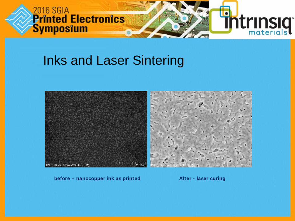
before – nanocopper ink as printed After - laser curing
Inks and Laser Sintering

18
Screen pastes are mixtures of micron and nano copper.Binders are optimized for rheology and adhesion
Screen Paste and Sintering

19
Laser Sintering of Cu NanoparticlesAmbient conditions, no oxidationSpin coated on GlassPattern height is 450 nm~ 4.5 µm wide linesρ = ~2 - 3X bulk Cu

20
Printing on Textiles
Eliminates traditional PCB creates functional parts. Were normally static.
21
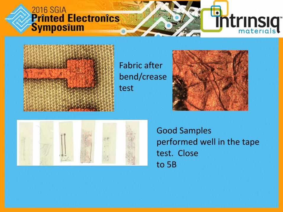
Good Samplesperformed well in the tape test. Closeto 5B
Fabric after bend/crease test

22
0.0
0.1
0.2
0.3
0.4
0.5
0 2 4 6 8 10 12
Tan 190
GP190-1 GP190-2 GP190-3
0.0
0.1
0.2
0.3
0.4
0.5
0 2 4 6 8 10 12
Sky Blue 190
Sky190-1 Sky190-2 Sky190-3
0.00.10.20.30.40.50.60.7
0 2 4 6 8 10 12
Tan 150
GP150-1 GP150-2 GP150-3
0.0
0.1
0.2
0.3
0.4
0.5
0.0 2.0 4.0 6.0 8.0 10.0 12.0
Sky Blue 150
Sky150-1 Sky150-2 Sky150-3
All Samples measure
Textile Bend/Crease Test - Graphical Results

23
Printing on Flexible Substrates
Paper, PET, Kapton, etc.

24
Screen Printing and Inkjet Printing Followed by Sintering
Material and Labor Cost Savings> 35%
Greener than photolith and plating procedures
5-7X Bulk Cu Resistivity Routinely, 3X in special cases
Kapton - Inkjet PET - Screen Print Paper- Flexography
Flex Circuit Substrate Examples

25
1 Micron Thick Copper Coating
Uniformly Sintered Copper on Rigid Epoxy Substrate

26
Post Sintered Ultra Thin Film on P.I.
• nano copper inks will achieve 0.5-2um thickness single or double sided.
• Most COTS flex materials are difficult to make ultra thin, or expensive. Thicker Films limit fine line, high density PCBs.
• The technology can be used on select ceramic and rigid FR4.
27
Printing and Sintering Equipment(partial list)
28
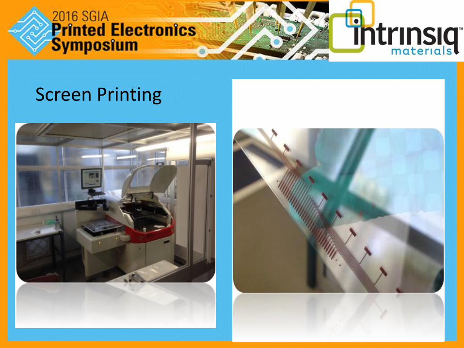
Screen Printing
29
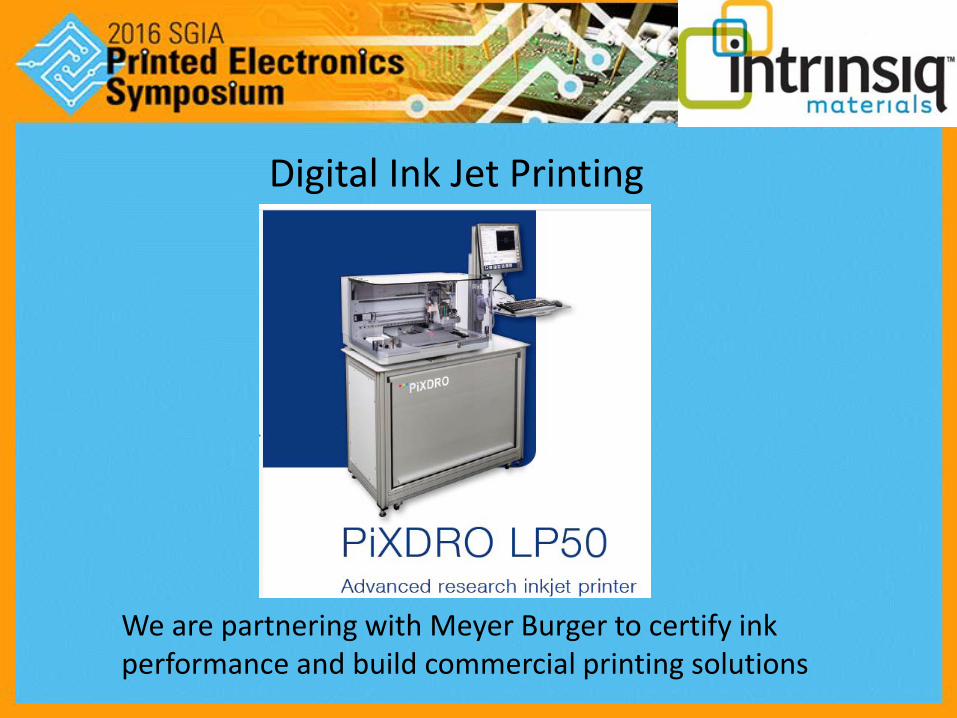
Digital Ink Jet Printing
We are partnering with Meyer Burger to certify ink performance and build commercial printing solutions

30
Drop Formation for Konica Minolta 4 pL Head at 5 kHz
• Well formed drops• Good directionality• No satellites

31
On Pulse Width 4 pL Printhead
Waveforms and print conditions developed by standard means

32
Example – Sinteron™ 2000Features
– Selectable pulse duration –100 to 2000 μm
– Adjustable Pulse energy 27 to 2000 Joules– Multiple modes – single,
double, burst, continuous– Sintering area 1.9 x 30.5cm
www.xenoncorp.com
Broadband Flash – Xenon Corporation
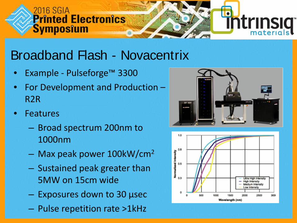
33
Broadband Flash - Novacentrix• Example - Pulseforge™ 3300• For Development and Production –
R2R• Features
– Broad spectrum 200nm to 1000nm
– Max peak power 100kW/cm2
– Sustained peak greater than 5MW on 15cm wide
– Exposures down to 30 μsec– Pulse repetition rate >1kHz

34
Laser Sintering Triple-wavelength Laser System does Selective Processing
Sinters Conductive Ink with 1.06µ wavelength fiber laser
Sinters over Near IR wavelength Range
Courtesy Universal Laser
35
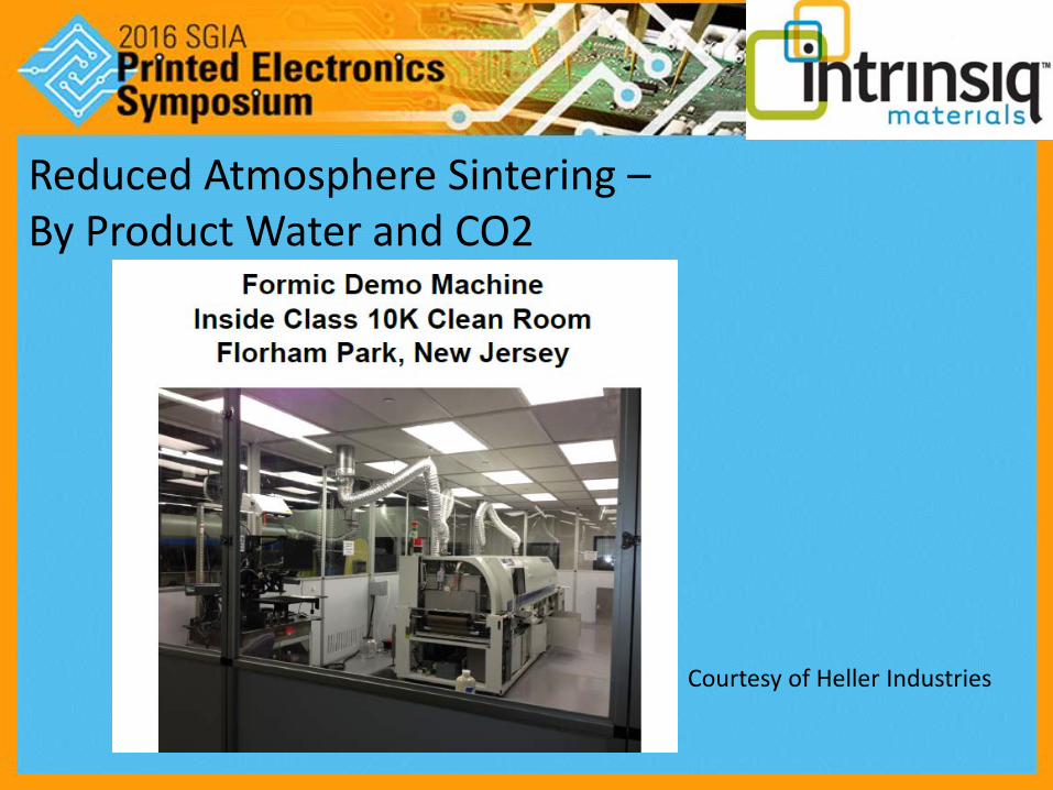
Reduced Atmosphere Sintering –By Product Water and CO2
Courtesy of Heller Industries

36
Slot Die Coating or Meyer Bar equipment
The coating is then dried and photonicallysintered using a flash lamp
37
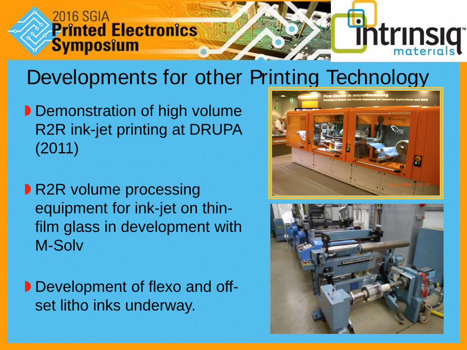
Developments for other Printing TechnologyDemonstration of high volume R2R ink-jet printing at DRUPA (2011)
R2R volume processing equipment for ink-jet on thin-film glass in development with M-Solv
Development of flexo and off-set litho inks underway.

38
Additional ProcessesEtching PlatingAblating

39
Plated and Etched Sample
• Panels were subjected to standard pattern plating process to produce circuitry and peel test coupons
• Pre-Clean, Dry Film Lamination, Image, Develop, Pattern plate, Tin Plate, Film Strip, Etch, Tin Strip
40
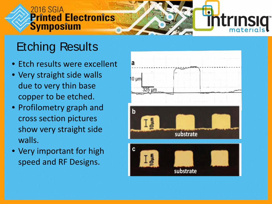
Etching Results• Etch results were excellent• Very straight side walls
due to very thin base copper to be etched.
• Profilometry graph and cross section pictures show very straight side walls.
• Very important for high speed and RF Designs.

41
Touch Display - Qualification Test Program Copper Bus bars with 20 micron wide
Contact and Bulk ResistivityAdhesionCustomer process integrationFunctional TestingEnvironmental Testing

42
CONCLUSIONS - DemonstratedPrinting on Fabrics non Traditional substrates - Textiles.Applications: Low Power, DC or Low Frequency Applications.Benefits: Eliminates traditional PCB lowers subassembly cost and weight.Printing on numerous traditional flexible substrates.Applications: Post Sintered Cu material dimensions and conductivities support low frequency/low current electronics applications.Benefits: Print on non traditional substrates – eliminate PCB weight and cost. Turn traditionally static parts into Functional electronic parts.
Select Plating and Etching nano Copper Ink and PasteApplications: High Power/Frequency Applications, Fine line ApplicationsBenefits: Higher Performance, Rapid Prototypes, High Signal Density
Proven equipment suppliers.
43
Thank you - Questions?
Contact:
Don NovotnyIntrinsiq MaterialsDNovotny@intqm(M) 619-517-0710