Nano strain gauge - SENSOR+TEST · Nanoparticles for measurement applications The nano strain gauge...
6
High sensitivity High resistance Miniaturized active area Nano strain gauge
Transcript of Nano strain gauge - SENSOR+TEST · Nanoparticles for measurement applications The nano strain gauge...

High sensitivityHigh resistance Miniaturized active area
Nano strain gauge
Nanoparticles for measurement applications
The nano strain gauge technology
Nanolike develops a new technology of nanoparticle-based nanosensors.
Thanks to the physical properties at nanoscale, nano strain gauges allow
to measure very thin deformations with both very low size and electrical
consumption.
Controlled deposition of nanoparticles between two gold electrodes make
very high sensitivity resistive nanosensors.
Example of a nano strain gauge(successive zooms)
©LPCNO©LPCNO
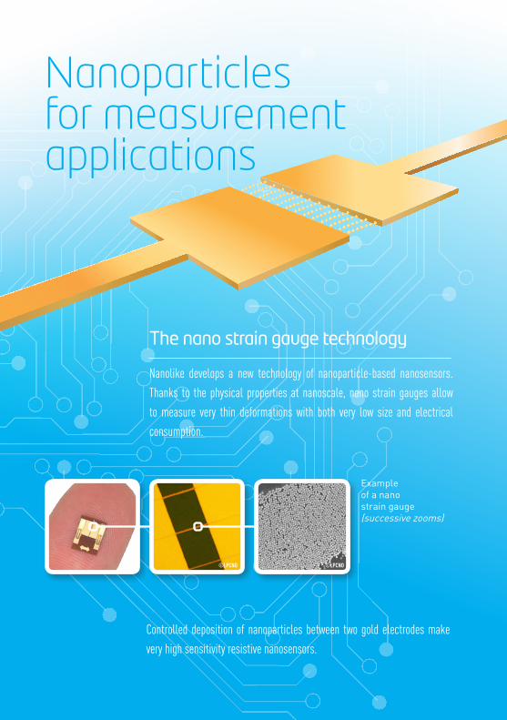
Integration becomes easierManufactured on flexible polyimide substrate, nano strain gauges are ready to be used in the same way as foil gauges.
More sensitive sensorsThanks to its very high gauge factor of 30, you can increase the sensitivity of your sensors.
Autonomous sensorsThe very low electrical consumption of the nano strain gauges brings you an opportunity to make autonomous wireless sensor network.
High sensitivityWith a gauge factor of 30, nano strain gauges bring an extremely high sensitivity for your measurements:
High resistance With nominal resistances up to 1MΩ, nano strain gauges have a very low electrical consumption less than 1 µW.
Miniaturized active areaWith an active area length around 100 µm, nano strain gauges allow you to make very precise and localized deformation measures.
The benefits of nanotechnologies
REMEMBER
Comparison of the active area surface
Comparison of the resistancevariation
Nanostrain gauge
Metallicgauge
Comparison of theelectrical consumption of different strain gauge technologies.
0.3 mm2
0.9 mm2 Foilgauge
Nanostrain gauge
0%
2%
4%
6%
8%
Strain
Rel
ativ
e re
sist
ance
var
iati
on
0,10%0% 0,20%
Nanosensor
Foil gauge
Semiconductor gauge
Electrical consumption
µW
10 mW
mW
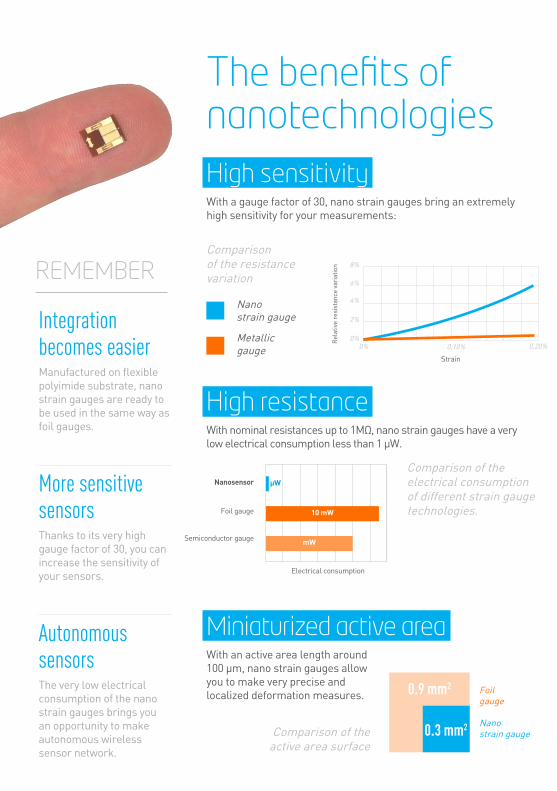
TechnicalSpecifications
Nano strain gauge (ref.)
a – Length of the active
area mm (in)
L – Length of the substrate
mm (in)
b – Width of the active
area mm (in)
w – Width of the substrate
mm (in)Resistance
NG-UNI-V3-200K0.1 (0.004) 7 (0.277) 3 (0.118) 6.5 (0.118)
200 kΩ
NG-UNI-V3-1M 1 M kΩ
• Shape of sensor response: ΔR/R0 = exp(g.ε)-1
• Gauge factor: g : 30• Nominal resistance: R : 200kΩ – 1M Ω• Deformation range: ε : 1 to 2 000 µm/m (limit: 0.2%)• Operating temperature : T : -40°C to +50°C Conditionning• Polarization voltage: typ. 0.5 – 1.5 V (CC)
• Possible conditionning configurations : Wheatstone bridge (full, half), voltage or current polarization, linear or logarithmic amplifier…
Conditionning with the plug-and-play NanoDAQ®
• Up to 6 nano strain gauges
• Temperature measurement and correction available
• USB serial output
Scheme of a nano strain gauge.
Welding AreaMaximum sensivity axis
L
W
a
b
NanoDAQ®: conditionning system for nanosensors
Foilgauge
Nanostrain gauge
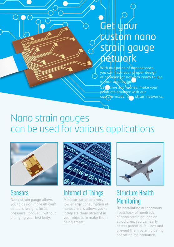
Nano strain gauges can be used for various applications
Get your custom nano strain gauge network
Nano strain gauge (ref.)
a – Length of the active
area mm (in)
L – Length of the substrate
mm (in)
b – Width of the active
area mm (in)
w – Width of the substrate
mm (in)Resistance
NG-UNI-V3-200K0.1 (0.004) 7 (0.277) 3 (0.118) 6.5 (0.118)
200 kΩ
NG-UNI-V3-1M 1 M kΩ
SensorsNano strain gauge allows you to design more efficient sensors (weight, force, pressure, torque...) without changing your test body.
Internet of ThingsMiniaturization and very low energy consumption of nanosensors allows you to integrate them straight in your objects to make them being smart.
Structure Health MonitoringBy installating autonomous «patches» of hundreds of nano strain gauges on structures, you can early detect potential failures and prevent them by anticipating operating maintenance.
With our patch of nanosensors, you can have your proper design of nanosensor network ready to use in your application.
Save time and money, make your products smarter with our custom-made nano strain networks.