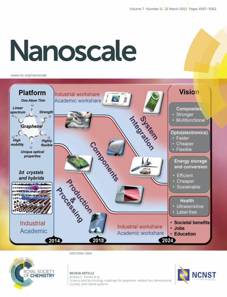
Nano Scale
214
Nanoscale www.rsc.org/nanoscale ISSN 2040-3364 REVIEW ARTICLE Andrea C. Ferrari et al. Science and technology roadmap for graphene, related two-dimensional crystals, and hybrid systems Volume 7 Number 11 21 March 2015 Pages 4587–5062
description
it is a good book on material science
Transcript of Nano Scale
Nanoscalewww.rsc.org/nanoscale
ISSN 2040-3364
REVIEW ARTICLEAndrea C. Ferrari et al.Science and technology roadmap for graphene, related two-dimensional crystals, and hybrid systems
Volume 7 Number 11 21 March 2015 Pages 4587–5062
Nanoscale
REVIEW
Cite this: Nanoscale, 2015, 7, 4598
Received 24th March 2014,Accepted 12th September 2014
DOI: 10.1039/c4nr01600a
www.rsc.org/nanoscale
Science and technology roadmap for graphene,related two-dimensional crystals, and hybridsystems
Andrea C. Ferrari,*a Francesco Bonaccorso,a,b Vladimir Fal’ko,c
Konstantin S. Novoselov,d Stephan Roche,e,f Peter Bøggild,g Stefano Borini,h
Frank H. L. Koppens,i Vincenzo Palermo,j Nicola Pugno,k,l,m José A. Garrido,n
Roman Sordan,o Alberto Bianco,p Laura Ballerini,q Maurizio Prato,r
Elefterios Lidorikis,s Jani Kivioja,h Claudio Marinelli,t Tapani Ryhänen,h
Alberto Morpurgo,u Jonathan N. Coleman,v,w Valeria Nicolosi,v,w,x Luigi Colombo,y
Albert Fert,z,aa Mar Garcia-Hernandez,ab Adrian Bachtold,i Grégory F. Schneider,ac
Francisco Guinea,ab Cees Dekker,ad Matteo Barbone,a Zhipei Sun,a
Costas Galiotis,ae,af Alexander N. Grigorenko,d Gerasimos Konstantatos,i Andras Kis,ag
Mikhail Katsnelson,ah Lieven Vandersypen,ad Annick Loiseau,ai Vittorio Morandi,aj
Daniel Neumaier,ak Emanuele Treossi,j Vittorio Pellegrini,b,al Marco Polini,al
Alessandro Tredicucci,al Gareth M. Williams,am Byung Hee Hong,an
Jong-Hyun Ahn,ao Jong Min Kim,ap Herbert Zirath,aq Bart J. van Wees,ar
Herre van der Zant,ad Luigi Occhipinti,as Andrea Di Matteo,as Ian A. Kinloch,at
Thomas Seyller,au Etienne Quesnel,av Xinliang Feng,aw Ken Teo,ax
Nalin Rupesinghe,ax Pertti Hakonen,ay Simon R. T. Neil,az Quentin Tannock,az
Tomas Löfwanderaq and Jari Kinaretba
We present the science and technology roadmap for graphene, related two-dimensional crystals, and hybrid
systems, targeting an evolution in technology, that might lead to impacts and benefits reaching into most
areas of society. This roadmap was developed within the framework of the European Graphene Flagship and
outlines the main targets and research areas as best understood at the start of this ambitious project. We
provide an overview of the key aspects of graphene and related materials (GRMs), ranging from fundamental
research challenges to a variety of applications in a large number of sectors, highlighting the steps necessary
to take GRMs from a state of raw potential to a point where they might revolutionize multiple industries. We
also define an extensive list of acronyms in an effort to standardize the nomenclature in this emerging field.
aCambridge Graphene Centre, University of Cambridge, Cambridge, CB3 0FA, UK.
E-mail: [email protected] Italiano di Tecnologia, Graphene Labs, Genova, 16163, ItalycDepartment of Physics, Lancaster University, Lancaster, LA1 4YB, UKdSchool of Physics and Astronomy, University of Manchester, Manchester, M13 9PL,
UKeICN2-Institut Catala de Nanociencia i Nanotecnologia, Campus UAB, 08193
Bellaterra (Barcelona), SpainfInstitució Catalana de Recerca i Estudis Avançats (ICREA), Barcelona,
08070, SpaingCentre for Nanostructured Graphene (CNG), Department of Micro- and
Nanotechnology, Technical University of Denmark, Lyngby, 2800, DenmarkhNokia Technologies, Broers Building, Cambridge, CB3 0FA, UKiInstitut de Ciències Fotòniques (ICFO), Castelldefels (Barcelona), 08860, SpainjCNR-Istituto per la Sintesi Organica e la Fotoreattività, Bologna, 40129, ItalykDipartimento di Ingegneria Civile, Ambientale e Meccanica, Università di Trento,
Trento, 38123, ItalylFondazione Bruno Kessler, Trento, 38122, Italy
mSchool of Engineering and Materials Science, Queen Mary University of London,
London, E1 4NS, UKnWalter Schottky Institut, Technische Universität München, Garching, 85748, GermanyoL-NESS, Dipartimento di Fisica, Politecnico di Milano, Como, 22100, ItalypCNRS, Institut de Biologie Moléculaire et Cellulaire, Immunopathologie et Chimie
Thérapeutique, 67000 Strasbourg, FranceqCentre for Neuroscience (BRAIN) and Dipartimento di Scienze della Vita, Università
di Trieste, Trieste, 34127, ItalyrDipartimento di Scienze Farmaceutiche, Università di Trieste, Trieste, 34127, ItalysDepartment of Materials Science and Engineering, University of Ioannina, Ioannina,
45110, GreecetApplied Graphene Materials, The Wilton Centre, Redcar, Cleveland, TS10 4RF, UKuDépartement de Physique de la Matière Condensée, Université de Genève, Geneva,
1205, SwitzerlandvSchool of Physics, Trinity College, Dublin, D2 Dublin, IrelandwCentre for Research on Adaptive Nanostructures and Nanodevices (CRANN), Trinity
College, Dublin, D2 Dublin, IrelandxSchool of Chemistry, Trinity College, Dublin, D2 Dublin, Ireland
4598 | Nanoscale, 2015, 7, 4598–4810 This journal is © The Royal Society of Chemistry 2015
Ope
n A
cces
s A
rtic
le. P
ublis
hed
on 2
2 Se
ptem
ber
2014
. Dow
nloa
ded
on 2
8/08
/201
5 13
:04:
01.
Thi
s ar
ticle
is li
cens
ed u
nder
a C
reat
ive
Com
mon
s A
ttrib
utio
n 3.
0 U
npor
ted
Lic
ence
.
View Article OnlineView Journal | View Issue

1. Introduction1.1. Graphene-based disruptive technologies: overview
1.1.1. Opportunities1.1.1.1. New opportunities for electronics1.1.1.2. New energy solutions1.1.1.3. New technologies and materials: towards a novel technological platform
1.2. Scientific output1.2.1. Intellectual property landscape analysis1.2.2. Graphene IP landscape analysis
2. Fundamental research2.1. Electronic transport2.2. Spectroscopic characterization2.3. Magnetism and spin transport2.4. Polycrystalline graphene2.5. Thermal and mechanical properties of graphene2.6. Artificial graphene structures in condensed-matter systems
2.6.1. Honeycomb lattices in semiconductors2.6.2. Honeycomb lattices with cold atoms
2.7. Atomic scale technology in graphene and patterned graphene2.7.1. Graphene nanoribbons2.7.2. Graphene quantum dots2.7.3. Patterning- and proximity-induced properties in graphene
2.8. 2d crystals beyond graphene2.8.1. Characterisation of new 2d crystals2.8.2. Modelling of physical properties of new 2d crystals
2.9. Hybrids of graphene and other 2d crystals2.9.1. Electronic transport in lateral and vertical hybrid superstructures
2.9.1.1. Tunnelling and resonant tunnelling devices2.9.1.2. Light emission and photovoltaics2.9.1.3. In situ characterization methods2.9.1.4. Hybrid structures for active plasmonics
2.10. Multiscale modelling of graphene-based structures and new 2d crystals2.10.1. Ab initio computations2.10.2. Mesoscale modelling2.10.3. High performance computing
yTexas Instruments Incorporated, Dallas, TX, USAzUnité Mixte de Physique CNRS/Thales, Palaiseau, 91767, FranceaaUniversité de Paris-Sud, Orsay, 91405, FranceabInstituto de Ciencia de Materiales de Madrid, CSIC, Madrid, 28049, SpainacLeiden University, Faculty of Science, Leiden Institute of Chemistry, Leiden 2333
CC, The NetherlandsadKavli Institute of Nanoscience, Delft University of Technology, Delft, 2628 CJ, The
NetherlandsaeInstitute of Chemical Engineering Sciences (ICE-HT/FORTH), Rio, 26504, GreeceafDepartment of Chemical Engineering, University of Patras, Rio, 26504, GreeceagElectrical Engineering Institute, Ecole Polytechique Fédérale de Lausanne,
Lausanne, 1015, SwitzerlandahInstitute for Molecules and Materials, Radboud University Nijmegen, Nijmegen,
6525 AJ, The NetherlandsaiLaboratoire d’Etude des Microstructures (LEM), ONERA-CNRS, Chatillon, 92322,
FranceajCNR-Istituto per la Microelettronica e i Microsistemi, Bologna, 40129, ItalyakAdvanced Microelectronic Centre Aachen, AMO GmbH, Aachen, 52074, GermanyalNEST, Istituto Nanoscienze-CNR and Scuola Normale Superiore, Pisa, 56127, ItalyamAirbus UK Ltd, Broughton, CH4 0DR, UK
anDepartment of Chemistry, Seoul National University, Seoul, 151-747, South KoreaaoSchool of Electrical & Electronic Engineering, Yonsei University, Seoul, 120-749,
South KoreaapDepartment of Engineering Science, University of Oxford, Oxford, OX1 3PJ, UKaqDepartment of Microtechnology and Nanoscience, Chalmers University of
Technology, Gothenburg, 412 96, SwedenarPhysics of Nanodevices, Zernike Institute for Advanced Materials, University of
Groningen, Groningen, 9747 AG, The NetherlandsasSTMicroelectronics, Arzano (Naples), 80022, ItalyatMaterials Science Centre, School of Materials, University of Manchester,
Manchester, M13 9PL, UKauInstitut für Physik, Technische Universität Chemnitz, Chemnitz, 09126, GermanyavInstitut LITEN, CEA LITEN, Grenoble Cedex 9, 38054 9, FranceawMax-Planck-Institut für Polymerforschung, Mainz, 55128, GermanyaxAixtron Ltd., Cambridge, UKayAalto University, FI-00076, FinlandazCambridgeIP, Cambridge, CB2 1SJ, UKbaDepartment of Applied Physics, Chalmers University of Technology, Gothenburg,
412 96, Sweden
Nanoscale Review
This journal is © The Royal Society of Chemistry 2015 Nanoscale, 2015, 7, 4598–4810 | 4599
Ope
n A
cces
s A
rtic
le. P
ublis
hed
on 2
2 Se
ptem
ber
2014
. Dow
nloa
ded
on 2
8/08
/201
5 13
:04:
01.
Thi
s ar
ticle
is li
cens
ed u
nder
a C
reat
ive
Com
mon
s A
ttrib
utio
n 3.
0 U
npor
ted
Lic
ence
.View Article Online

2.10.4. Further development of field-theory and kinetic theory methods2.10.5. Correlations in multiple graphene layers
2.11. Graphene for high-end instrumentation2.11.1. Graphene for high energy physics instrumentation, Tokamaks and Stellarators2.11.2. Graphene for metrology
2.11.2.1. Quantum resistance2.11.2.2. Quantum current standard2.11.2.3. Standard for optical absorption coefficient
2.12. Perspectives
3. Health and environment3.1. In vitro impact3.2. Cytotoxicity effects on graphene-coated surfaces3.3. In vivo impact, biodistribution and pharmacokinetics3.4. Bacterial toxicity3.5. Biodegradation3.6. Environmental impact3.7. 2d crystals and hybrids3.8. Perspective
4. Production4.1. Graphene production
4.1.1. Dry exfoliation4.1.1.1. Mechanical exfoliation for research purposes and new concept devices4.1.1.2. Anodic bonding4.1.1.3. Laser ablation and photoexfoliation
4.1.2. Liquid phase exfoliation4.1.2.1. LPE of graphite4.1.2.2. LPE of graphite oxide4.1.2.3. LPE of intercalated graphite
4.2. Growth on SiC4.3. Growth on metals by precipitation4.4. Chemical vapour deposition
4.4.1. Thermal CVD on metals4.4.2. CVD on semiconductors and insulators4.4.3. Plasma enhanced CVD
4.5. Molecular beam epitaxy growth of graphene on insulating surfaces4.6. Atomic layer epitaxy4.7. Heat-driven conversion of amorphous carbon and other carbon sources4.8. Chemical synthesis4.9. Nano-ribbons and quantum dots4.10. Transfer and placement
4.10.1. Transfer, placement and shaping4.10.2. Graphene membranes4.10.3. Transfer of individual layers4.10.4. Wet transfer of exfoliated flakes4.10.5. Dry transfer of exfoliated flakes4.10.6. Transfer of graphene grown on metals4.10.7. Di-electrophoresis4.10.8. Applications and processing of graphene inks
4.11. Contamination and cleaning4.11.1. Cleaning of graphene produced by MC4.11.2. Cleaning after transfer4.11.3. Removal of solvents/surfactants in LPE graphene
Review Nanoscale
4600 | Nanoscale, 2015, 7, 4598–4810 This journal is © The Royal Society of Chemistry 2015
Ope
n A
cces
s A
rtic
le. P
ublis
hed
on 2
2 Se
ptem
ber
2014
. Dow
nloa
ded
on 2
8/08
/201
5 13
:04:
01.
Thi
s ar
ticle
is li
cens
ed u
nder
a C
reat
ive
Com
mon
s A
ttrib
utio
n 3.
0 U
npor
ted
Lic
ence
.View Article Online
4.12. Inorganic layered compounds4.12.1. Mechanical cleavage4.12.2. Laser ablation4.12.3. Liquid phase exfoliation4.12.4. Synthesis by thin film techniques
4.13. Graphene and other 2d crystal hybrids4.13.1. CVD growth of heterostructures4.13.2. Mechanical transfer4.13.3. Heterostructures from dispersions and inks4.13.4. Bonding using polymers
4.14. Silicene, germanene, phosphorene, MXene and other graphene like systems4.14.1. Chemical modification of 2d crystals
4.15. Outlook and future challenges
5. Electronic devices5.1. Opening a band-gap in graphene5.2. Graphene-based microelectronics and nanoelectronics
5.2.1. Transistor count in graphene circuits5.2.2. Digital logic gates5.2.3. Digital non-volatile memories5.2.4. Interconnects in integrated circuits
5.3. High frequency electronics5.3.1. Analogue voltage amplifiers5.3.2. Graphene ring oscillators
5.4. Layered materials-based devices5.5. Novel vertical and planar transistors and devices
5.5.1. Vertical tunnelling transistors and vertical hot electron transistors5.5.2. In-plane transport in 2d heterostructures
5.6. Electron emission
6. Spintronics6.1. Graphene spintronics6.2. Spin injection in graphene6.3. Graphene spintronic devices for sensing6.4. Graphene spin gating6.5. Graphene qubits6.6. Spintronics using other 2d crystals and heterostructures6.7. Theory and quantum simulation6.8. Outlook
7. Photonics and optoelectronics7.1. Graphene saturable absorbers and related devices
7.1.1. 2d crystals-based saturable absorbers7.1.2. Output power/pulse energy7.1.3. Spectral coverage7.1.4. Pulse width7.1.5. Repetition rate7.1.6. Other considerations
7.2. Photodetectors7.2.1. Figures of merit7.2.2. Physical mechanisms enabling photodetection
7.2.2.1. Photovoltaic effect7.2.2.2. Photo-thermoelectric effect7.2.2.3. Bolometric effect7.2.2.4. Photogating effect7.2.2.5. Plasma-wave-assisted mechanism
Nanoscale Review
This journal is © The Royal Society of Chemistry 2015 Nanoscale, 2015, 7, 4598–4810 | 4601
Ope
n A
cces
s A
rtic
le. P
ublis
hed
on 2
2 Se
ptem
ber
2014
. Dow
nloa
ded
on 2
8/08
/201
5 13
:04:
01.
Thi
s ar
ticle
is li
cens
ed u
nder
a C
reat
ive
Com
mon
s A
ttrib
utio
n 3.
0 U
npor
ted
Lic
ence
.View Article Online
7.2.3. Photoelectrical response in different devices7.2.3.1. Bolometers7.2.3.2. Long-wavelength photodetectors7.2.3.3. 2d crystals and hybrids
7.2.4. Challenges and perspectives in photodetector devices7.3. Graphene plasmonics
7.3.1. Hybrid graphene-plasmon systems7.3.2. Intrinsic graphene plasmons
7.4. Graphene-based antennas7.5. Hybrid graphene-nanocrystal for light emitting devices7.6. Graphene-based nanoscale optical routing and switching networks
8. Sensors8.1. Contact sensors
8.1.1. Nanoelectromechanical sensors8.1.2. Chemical sensors
8.2. Non-contact sensors8.2.1. Microwave detectors8.2.2. Fast charge detectors8.2.3. Strain sensors8.2.4. Magnetic sensors8.2.5. Signal processing in ballistic graphene-based devices
8.3. 2d crystals and hybrids8.3.1. Chemical sensors
9. Flexible electronics9.1. Key technology enablers9.2. Innovative flexible devices and user interfaces for consumer electronics
9.2.1. Transparent conductive films9.2.2. Production of graphene transparent conductive films9.2.3. Mechanical performance of transparent films for flexible electronics9.2.4. Applications of graphene transparent conductive films9.2.5. 2d crystals and hybrids for flexible electronics
9.3. Outlook
10. Energy storage and conversion10.1. Batteries10.2. Supercapacitors10.3. Fuel cells and hydrogen storage10.4. Graphene solar cells10.5. Thermoelectric devices10.6. Nanogenerators
11. Composites11.1. Polymer-based composites11.2. Ceramic-based composites11.3. 2d organic and inorganic nanocomposites based on chemically modified graphene11.4. Photonic polymer composites
12. Biomedical applications12.1. Imaging and diagnosis12.2. Hyperthermia: photothermal ablation of tumours12.3. Targeted drug delivery12.4. Gene transfection12.5. Bioelectronics and biosensors12.6. Thin films, joint prostheses
Review Nanoscale
4602 | Nanoscale, 2015, 7, 4598–4810 This journal is © The Royal Society of Chemistry 2015
Ope
n A
cces
s A
rtic
le. P
ublis
hed
on 2
2 Se
ptem
ber
2014
. Dow
nloa
ded
on 2
8/08
/201
5 13
:04:
01.
Thi
s ar
ticle
is li
cens
ed u
nder
a C
reat
ive
Com
mon
s A
ttrib
utio
n 3.
0 U
npor
ted
Lic
ence
.View Article Online
12.7. Single-molecule genomic screening devices12.8. Plasmonic biosensors
12.8.1. Utilizing graphene’s intrinsic plasmons12.8.2. Graphene as a functionalization-passivation gate-tuneable coating12.8.3. Graphene as a direct transducer
13. Conclusions
List of acronyms
0d Zero dimensional1d One-dimensional1LG Single layer graphene1L-MoS2 Single layer molybdenum disulfide2d Two-dimensional2D Overtone of Raman D peak2DEG Two-dimensional electron gas2LG Two-layer graphene2L-MoS2 Two-layer molybdenum disulfide3d Three-dimensional3LG Tri-layer graphene3L-MoS2 Tri-layer molybdenum disulfideα Absorption coefficientAabs Absorbed photon fractiona-C Amorphous carbona-C:H Hydrogenated amorphous carbonA/D Analog to digitalAFM Atomic force microscopyAG Artificial grapheneAg SilverALD Atomic layer depositionALE Atomic Layer EpitaxyAl2O3 Aluminium oxideAPD Avalanche photodiodeAr ArgonARPES Angle-resolved photoemission spectroscopyAu GoldAV Voltage GainAV Alternating voltageBC Block copolymerBGI Broken Galilean invarianceBISFET Bilayer pseudospin field effect transistorBLG Bi-layer grapheneBMIMPF6 1-Butyl-3-methylimidazolium hexafluorophosphateB3N3H6 BorazineBi2Se3 Bismuth selenideBi2Te3 Bismuth tellurideBN Boron nitridec ConcentrationCBE Chemical beam epitaxyc–BN Cubic–boron nitrideCdS Cadmium sulfideCdSe Cadmium selenideCE Counter electrodeCERN European organization for nuclear research
C-face Carbon faceCFRC Ceramic fiber reinforced concreteCIN Colloidal inorganic nanocrystalCl ChlorineCMG Chemically modified grapheneCMOS Complementary metal oxide semiconductorCNP Carbon nanoparticleCNT Carbon nanotubeCNW Carbon nanowallCo CobaltCSG Covalently bound stretched grapheneCu CopperCVD Chemical vapour depositionCVFF Consistent valence force fieldγ Surface tensionD Raman D peakD* Specific detectivityDC Direct currentDDA Discrete dipole approximationDFPT Density functional perturbation theoryDFT Density functional theoryDGM Density gradient mediumDGU Density gradient ultracentrifugationDLC Diamond-like carbonDMF DimethylformamideDMMP DimethylmethylphosphonateDNA Deoxyribonucleic acidDoE Department of Energy-USADP Dyakonov-PerelDS Dyakonov-ShurDSSC Dye-sensitized solar cellD-WDM Dense wavelength division multiplexerηabs Light absorption efficiencyEELS Electron energy loss spectroscopyEDFA Erbium-doped fibre amplifierEDFL Erbium-doped fiber laserEDLC Electrochemical double layer capacitore–e Electron–electrone–h electron–holeEY Eliot–YafetEGFP Enhanced green fluorescence proteinEHF Extremely high frequencyEM ElectromagneticEMI Electromagnetic interferenceEph Photon energyEPO European patent officeEPR Electric paramagnetic resonance
Nanoscale Review
This journal is © The Royal Society of Chemistry 2015 Nanoscale, 2015, 7, 4598–4810 | 4603
Ope
n A
cces
s A
rtic
le. P
ublis
hed
on 2
2 Se
ptem
ber
2014
. Dow
nloa
ded
on 2
8/08
/201
5 13
:04:
01.
Thi
s ar
ticle
is li
cens
ed u
nder
a C
reat
ive
Com
mon
s A
ttrib
utio
n 3.
0 U
npor
ted
Lic
ence
.View Article Online

EPRE Enhanced permeability and retention effectEQE External quantum efficiencyERMD Emerging research memory deviceET Electro–tactileηtrans charge transfer efficiencyFDTD Finite-difference time-domainFE Field emissionFET Field effect transistorFF Fill factorFG Functionalized grapheneFIR Far infraredFLG Few-layer grapheneFPA Focal plane arrayFQHE Fractional quantum hall effectFTO Fluorine-doped tin oxideZ Field enhancement factorG Raman G peakGaAs Gallium arsenideGaN Gallium nitrideGB Grain boundaryGBL γ-Butyrolactonegd Output conductanceGD Gravimetric densityGFET Graphene field-effect transistorGFRC Glass fiber reinforced concreteGHz Giga HertzGIC Graphite intercalation compoundgm TransconductanceGND GroundGNR Graphene nanoribbonGO Graphene oxideGOQD Graphene oxide quantum dotGOTCF Graphene oxide transparent conductive filmGPD Graphene-based photodetectorGph Photocondutive gainGQD Graphene quantum dotGRMs Graphene and related materialsGRO Graphene ring oscillatorGSA Graphene saturable absorberGSAM Graphene saturable absorber mirrorGTCE Graphene transparent conductive electrodeGTCF Graphene transparent conductive filmGWC Graphene-enabled wireless communicationsHBC Hexa-perihexabenzocoroneneh-BN Hexagonal boron nitrideHCI Human computer interactionHCl Hydrochloric acidhcp Hexagonal closed packedH2 HydrogenHe HeliumHeLa Henrietta LacksHEMT High-electron mobility transistorHF High frequencyH–F Hartree–FockHfO2 Hafnium oxide
HMIH 1-Hexyl-3-methylimidazoliumhexafluorophosphate
HOMO Highest occupied molecular orbitalHPC High performance computingHRTEM High resolution transmission electron microscopeHSC Hybrid supercapacitorK Potassiumκ Thermal conductivityK Dielectric constantKOH Potassium hydroxideICP Inductively coupled plasmaICT Information and communications technologyIL Ionic liquidIn IndiumIn2O3 Indium oxideION/IOFF On/Off current ratioInP Indium phosphideInSb Indium antimonideIP Intellectual PropertyIph PhotocurrentIQE Internal quantum efficiencyIR InfraredIr IridiumITO Indium tin oxideITRS International technology roadmap for
semiconductorsLaB6 Lanthanum hexaborideLC Liquid crystalLED Light emitting diodeLEED Low-energy electron diffractionLi LithiumLIB Lithium ion batteryLM Layered materialLNA Low-noise amplifierLO Local oscillatorLPCVD Low pressure chemical vapour depositionLPE Liquid phase exfoliationLSPR Localized surface plasmon resonanceLUMO Lowest unoccupied molecular orbitalµ Carrier mobilitym Staging indexMAC Medium access controlMBE Molecular beam epitaxyMC Micromechanical cleavageMCC Mesoporous carbon capsuleMC-SLG Mechanically cleaved-single layer grapheneMD Molecular dynamicsMEGrO Microwave expanded graphite oxideMEMS Micro electro-mechanical systemsMESFET Metal-semiconductor field effect transistorMGM Metal-graphene-metalMgO Magnesium oxideMIR Mid-infraredMLG Multilayer grapheneMnO2 Manganese dioxide
Review Nanoscale
4604 | Nanoscale, 2015, 7, 4598–4810 This journal is © The Royal Society of Chemistry 2015
Ope
n A
cces
s A
rtic
le. P
ublis
hed
on 2
2 Se
ptem
ber
2014
. Dow
nloa
ded
on 2
8/08
/201
5 13
:04:
01.
Thi
s ar
ticle
is li
cens
ed u
nder
a C
reat
ive
Com
mon
s A
ttrib
utio
n 3.
0 U
npor
ted
Lic
ence
.View Article Online
MNP Metallic nanoparticleMOCVD Metal–organic chemical vapour depositionMoS2 Molybdenum disulfideMoSe2 Molybdenum diselenideMOSFET Metal–oxide-semiconductor field-effect transistorMoTe2 Molybdenum ditellurideMRAM Magnetoresistive random-access memoryMSSC Meso-super-structured solar cellm-SWNT Metallic single wall carbon nanotubeMTJ Magnetic tunnel junctionMWCVD Micro wave chemical vapour depositionν Viscosityn carrier densityN Number of layersNaOH Sodium hydroxideNbSe2 Niobium diselenideNEM Nano electromechanicalNEMS Nano electromechanical systemsNEP Noise equivalent powerNG NanogeneratorNi NickelNIR Near infraredNiTe2 Nickel ditellurideNLG N-layer grapheneNMP N-MethylpyrrolidoneNOEMS Nano optoelectromechanical systemsNP Nano-particleNR NanoribbonNW NanowireOAS Optical absorption spectroscopyOLED Organic light-emitting diodeO(N) Computations scaling linearly with the number of
atomsO(N3) Computations scaling with the cube of the
number of atomsOPV Organic photo-voltaicOT Optical tweezersO2 Oxygenϕabs absorbed photon fluxϕin incoming photon fluxP3HT Poly-3-hexyl thiophenePA6 Polyamide6 (also known as Nylon6)PAN PolyacrylonitrilePAHs Poly-aromatic hydrocarbonsPbS Lead sulphidePC PhotocurrentPCa PolycarbonatePCBM Phenyl-C61-butyric acid methyl esterPCF Photonic crustal fiberPCL PolycaprolactonePCT Patent cooperation treatyPD PhotodetectorPDMS Poly(dimethylsiloxane)P/E Program/erasePECVD Plasma enhanced chemical vapour deposition
PEDOT poly(3,4 ethylenedioxythiophene)PEG Polyethylene glycolPEO Polyethylene glycolPEI PolyethyleneiminePEN Polyethylene naphthalatePET Polyethylene terephthalatePd PalladiumPDLC Polymer dispersed liquid crystalPDMS PolydimethylsiloxanepDNA Plasmid deoxyribonucleic acidPin Incident powerPH–F Post-Hartree–FockPIL:RGO poly(ionic liquid)-modified reduced graphene oxidePL PhotoluminescencePMF Polarization-maintaining fiberPMMA PolymethylmethacrylatePMT Photomultiplier tubePP Poly-propylenePNF Polyaniline NanofiberPPC Poly-propylene carbonatePRACE Partnership for advanced computing in EuropePS PolystyrenePSS Polystyrene sulphonatePt PlatinumPTCDA Perylene-3,4,9,10-tetracarboxylic dianhydridePTE Photothermo-electricPTFE PolytetrafluoroethylenePV PhotovoltaicPVA PolyvinylalcoholPVC Polyvinyl chloridePVD Physical vapour depositionPVDF Polyvinyl difluoridePZT Piezoelectricq Electron chargeQD Quantum dotQE Quantum efficiencyQHE Quantum Hall effectQMC Quantum Monte CarloQM/MM Quantum mechanics/molecular mechanicsQPC Quantum point contactQSH Quantum spin HallQSHE Quantum spin Hall effectρ DensityRCA Radio corporation of AmericaR&D Research and developmentRES Reticuloendothelial systemRF Radio frequencyRGO Reduced graphene oxideRIXS Resonant inelastic X-ray scatteringRNA Ribonucleic acidRO Ring oscillatorROIC Read-out integrated circuitsROS Reactive oxygen speciesRph ResponsivityRPA Random phase approximation
Nanoscale Review
This journal is © The Royal Society of Chemistry 2015 Nanoscale, 2015, 7, 4598–4810 | 4605
Ope
n A
cces
s A
rtic
le. P
ublis
hed
on 2
2 Se
ptem
ber
2014
. Dow
nloa
ded
on 2
8/08
/201
5 13
:04:
01.
Thi
s ar
ticle
is li
cens
ed u
nder
a C
reat
ive
Com
mon
s A
ttrib
utio
n 3.
0 U
npor
ted
Lic
ence
.View Article Online
R2R Roll to rollRs Sheet resistanceRT Room temperatureRu RutheniumRZS Rate zonal separationς Surface energyσ Electrical conductivityS Seebeck coefficientSA Saturable absorberSAM Self-assembled monolayerSAN Styrene-acrylonitrileSbF5 Antimony pentafluorideSBS Sedimentation based-separationSC Sodium cholateSCM Scanning catalyst microscopeSDBS Sodium dodecyl benzene sulfonateSDC Sodium deoxycholateSDS Sodium dodecyl sulphateSEI Solid electrolyte interphaseSEIRA Surface-enhanced infrared Raman absorptionSESAM Semiconductor saturable absorber mirrorSERS Surface enhanced Raman spectroscopySET Single electron transistorSEY Secondary electron yieldSHE Spin Hall effectSi SiliconSiC Silicon carbideSi/Ge Silicon/germaniunSiO2 Silicon dioxideSiRNA Small interfering ribonucleic acidSLG Single layer grapheneSMMA Styrene methyl methacrylateSnO2 Tin oxideSO Spin orbitSOI Silicon-on-insulatorSPP Surface plasmon polaritonSPR Surface plasmon resonanceSQD Semiconductor quantum dotSQUID Superconducting quantum interference deviceSSA Specific surface areassDNA Single-stranded DNAs-SNOM Scattering-type near-field microscopyST Science and technologySTEM Scanning transmission electron microscopySTM Scanning tunnelling microscopySTR Science and technology roadmapSTS Scanning tunnelling spectroscopySTT Spin transfer torqueSWIR Short wavelength infraredSWNT Single wall carbon nanotubes-SWNT Semiconducting single wall carbon nanotubeT Temperatureta-C Tetrahedral amorphous carbonta-C:H Hydrogenated tetrahedral amorphous carbonta-C:N Nitrogenated tetrahedral amorphous carbon
TaSe2 Tantalum selenideTc Critical temperatureTC Transparent conductorTCE Transparent conductor electrodeTCF Transparent conductor filmTDDFT Time-dependent density functional theoryTe Electron temperatureTEM Transmission electron microscopeTGA Thermo-gravimetric analysisTHz Tera-HertzTi TitaniumTI Topological insulatorTiO2 Titanium dioxideTLG Trilayer grapheneTM Transverse magneticTMD Transition metal dichalcogenideTMO Transition metal oxideTPU Thermoplastic polyurethaneTr TransmittanceTRL Technology readiness levelτtr Charge lifetimeτtransit Drift transit timeUHV Ultra-high vacuumUI User interfaceULGA Ultralight and highly compressible graphene aerogelsUS PTO United States patent and trademark officeUV UltravioletVCD Vibrational circular dichroismVD Volumetric densityvdW van der WaalsvH van Hove singularityVRH Variable range hoppingWDM Wavelength division multiplexerWIPO World intellectual property organizationWNSN Wireless nanosensor networkWO2 Tungsten dioxideWS Tungsten sulfideWS2 Tungsten disulfideXAS X-ray absorption spectroscopyXMCD X-ray magnetic circular dichroismXPS X-ray photoelectron spectroscopyYM Yield by SLG percentageYW Yield by weightYWM Yield by SLG weightζ Field enhancement factorZnO Zinc oxideZnS Zinc sulfideZnSe Zinc selenide
1. Introduction
The primary objective of this roadmap is to guide the commu-nity towards the development of products based on graphene,related two dimensional (2d) crystals and hybrid systems. Forsimplicity we will refer to this new materials platform as
Review Nanoscale
4606 | Nanoscale, 2015, 7, 4598–4810 This journal is © The Royal Society of Chemistry 2015
Ope
n A
cces
s A
rtic
le. P
ublis
hed
on 2
2 Se
ptem
ber
2014
. Dow
nloa
ded
on 2
8/08
/201
5 13
:04:
01.
Thi
s ar
ticle
is li
cens
ed u
nder
a C
reat
ive
Com
mon
s A
ttrib
utio
n 3.
0 U
npor
ted
Lic
ence
.View Article Online

graphene and relatedmaterials and use the acronym GRM. Thesehave a combination of properties that could make them keyenablers for many applications, generating new products thatcannot (or may be difficult to) be obtained with current techno-logies or materials. The creation of new disruptive technologiesbased on GRMs is conditional to reaching a variety of objectivesand overcoming several challenges throughout the value chain,ranging frommaterials to components and systems.
The main scientific and technological objectives are:A) Material technologies
○ Identification of new layered materials (LMs) andassessment of their potential.
○ Reliable, reproducible, sustainable and safe, large scaleproduction of GRMs, satisfying the specific needs of differentapplication areas.
B) Component technologies○ Identification of new device concepts enabled by GRMs.○ Identification of component technologies that utilize
GRMs.○ Electronic technologies, comprising high frequency
electronics, optoelectronics, spintronics and sensors.C) Systems integration
○ Route to bring components and structures based onGRMs to systems capable of providing new functionalities andopen new application areas.
○ New concepts for integrating GRMs in existing technol-ogy platforms.
○ Integration routes for nanocomposites, flexible elec-tronics and energy applications.
Our science and technology roadmap (STR) outlines theprincipal routes to develop the GRM knowledge base and themeans of production and development of new devices, withthe final aim of integrating GRMs into systems. In the Infor-mation and Communications Technology (ICT) area, the STRfocuses on technology that will enable new applications, such asthe Morph concept1 (Fig. 1a), which exploits the electrical,optical and mechanical properties of GRMs to realize new typesof personal communicators. In the domain of physical com-munication, the STR targets several key technologies in energyproduction and storage, as well as new functional light-weightcomposites. These are to be integrated in transportation
systems, such as new airplanes, buses, cars (as illustrated by theSmartForVision concept electric car,2 Fig. 1b). The STR also con-siders areas such as Health and Energy. By exploiting the GRM’sunique electrical and optical properties, the STR will highlightthe directions towards the development of novel systems forinformation processing and communications.
The STR is divided in 11 thematic chapters, summarized inFig. 2. Each of them comprises a dedicated timeline. A finalchapter presents two overall summary roadmaps.
The present STR may not be fully complete, leaving outsome of the most recent and rapidly evolving areas. We plan topresent regular updates over the next 10 years to keep abreastwith the latest developments in GRM science and technology.
Fig. 2 Symbols associated with each theme. In the document, the
symbol is associated/replaced by the symbol when we refer
to industrial/large scale production.
Fig. 1 Morph1 (left) and SmartForVision2 (right) are examples of visionary applications where GRMs’ unique properties might be combined to enablenew products.
Nanoscale Review
This journal is © The Royal Society of Chemistry 2015 Nanoscale, 2015, 7, 4598–4810 | 4607
Ope
n A
cces
s A
rtic
le. P
ublis
hed
on 2
2 Se
ptem
ber
2014
. Dow
nloa
ded
on 2
8/08
/201
5 13
:04:
01.
Thi
s ar
ticle
is li
cens
ed u
nder
a C
reat
ive
Com
mon
s A
ttrib
utio
n 3.
0 U
npor
ted
Lic
ence
.View Article Online
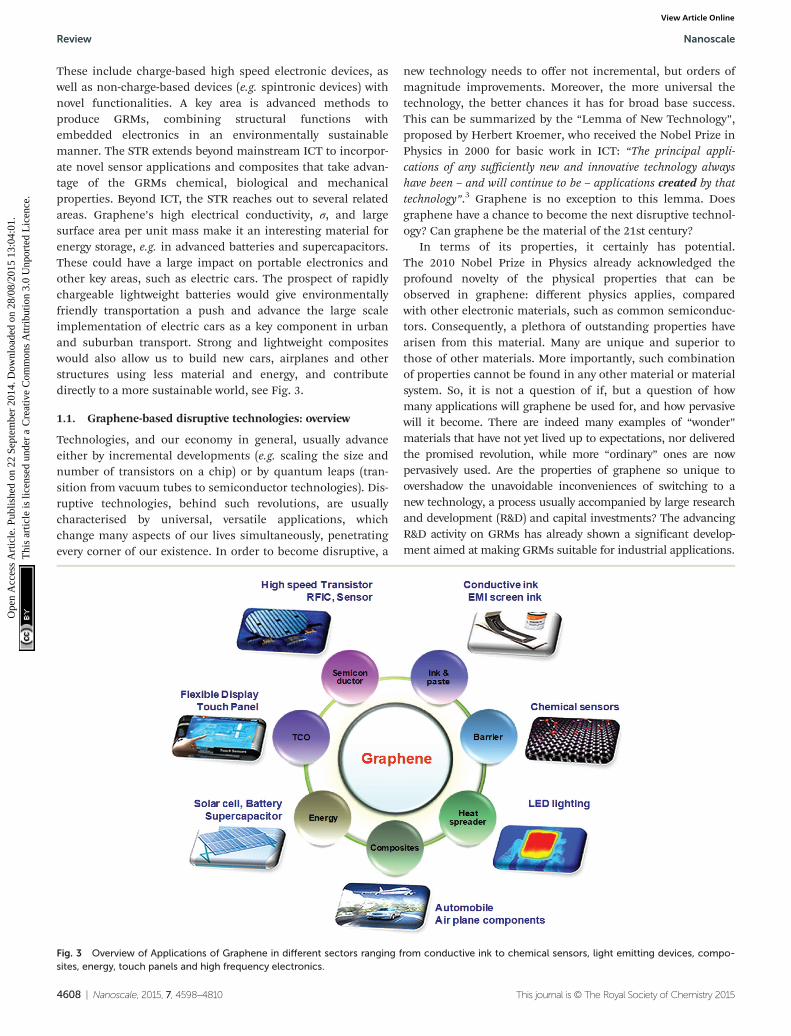
These include charge-based high speed electronic devices, aswell as non-charge-based devices (e.g. spintronic devices) withnovel functionalities. A key area is advanced methods toproduce GRMs, combining structural functions withembedded electronics in an environmentally sustainablemanner. The STR extends beyond mainstream ICT to incorpor-ate novel sensor applications and composites that take advan-tage of the GRMs chemical, biological and mechanicalproperties. Beyond ICT, the STR reaches out to several relatedareas. Graphene’s high electrical conductivity, σ, and largesurface area per unit mass make it an interesting material forenergy storage, e.g. in advanced batteries and supercapacitors.These could have a large impact on portable electronics andother key areas, such as electric cars. The prospect of rapidlychargeable lightweight batteries would give environmentallyfriendly transportation a push and advance the large scaleimplementation of electric cars as a key component in urbanand suburban transport. Strong and lightweight compositeswould also allow us to build new cars, airplanes and otherstructures using less material and energy, and contributedirectly to a more sustainable world, see Fig. 3.
1.1. Graphene-based disruptive technologies: overview
Technologies, and our economy in general, usually advanceeither by incremental developments (e.g. scaling the size andnumber of transistors on a chip) or by quantum leaps (tran-sition from vacuum tubes to semiconductor technologies). Dis-ruptive technologies, behind such revolutions, are usuallycharacterised by universal, versatile applications, whichchange many aspects of our lives simultaneously, penetratingevery corner of our existence. In order to become disruptive, a
new technology needs to offer not incremental, but orders ofmagnitude improvements. Moreover, the more universal thetechnology, the better chances it has for broad base success.This can be summarized by the “Lemma of New Technology”,proposed by Herbert Kroemer, who received the Nobel Prize inPhysics in 2000 for basic work in ICT: “The principal appli-cations of any sufficiently new and innovative technology alwayshave been – and will continue to be – applications created by thattechnology”.3 Graphene is no exception to this lemma. Doesgraphene have a chance to become the next disruptive technol-ogy? Can graphene be the material of the 21st century?
In terms of its properties, it certainly has potential.The 2010 Nobel Prize in Physics already acknowledged theprofound novelty of the physical properties that can beobserved in graphene: different physics applies, comparedwith other electronic materials, such as common semiconduc-tors. Consequently, a plethora of outstanding properties havearisen from this material. Many are unique and superior tothose of other materials. More importantly, such combinationof properties cannot be found in any other material or materialsystem. So, it is not a question of if, but a question of howmany applications will graphene be used for, and how pervasivewill it become. There are indeed many examples of “wonder”materials that have not yet lived up to expectations, nor deliveredthe promised revolution, while more “ordinary” ones are nowpervasively used. Are the properties of graphene so unique toovershadow the unavoidable inconveniences of switching to anew technology, a process usually accompanied by large researchand development (R&D) and capital investments? The advancingR&D activity on GRMs has already shown a significant develop-ment aimed at making GRMs suitable for industrial applications.
Fig. 3 Overview of Applications of Graphene in different sectors ranging from conductive ink to chemical sensors, light emitting devices, compo-sites, energy, touch panels and high frequency electronics.
Review Nanoscale
4608 | Nanoscale, 2015, 7, 4598–4810 This journal is © The Royal Society of Chemistry 2015
Ope
n A
cces
s A
rtic
le. P
ublis
hed
on 2
2 Se
ptem
ber
2014
. Dow
nloa
ded
on 2
8/08
/201
5 13
:04:
01.
Thi
s ar
ticle
is li
cens
ed u
nder
a C
reat
ive
Com
mon
s A
ttrib
utio
n 3.
0 U
npor
ted
Lic
ence
.View Article Online
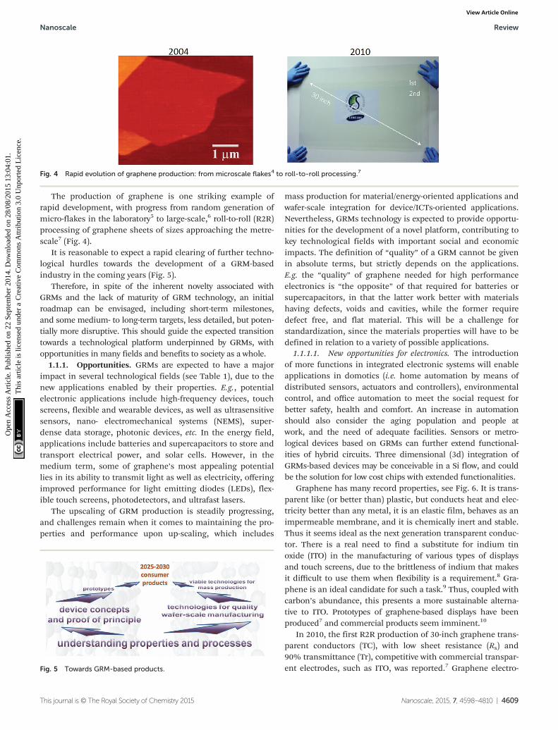
The production of graphene is one striking example ofrapid development, with progress from random generation ofmicro-flakes in the laboratory5 to large-scale,6 roll-to-roll (R2R)processing of graphene sheets of sizes approaching the metre-scale7 (Fig. 4).
It is reasonable to expect a rapid clearing of further techno-logical hurdles towards the development of a GRM-basedindustry in the coming years (Fig. 5).
Therefore, in spite of the inherent novelty associated withGRMs and the lack of maturity of GRM technology, an initialroadmap can be envisaged, including short-term milestones,and some medium- to long-term targets, less detailed, but poten-tially more disruptive. This should guide the expected transitiontowards a technological platform underpinned by GRMs, withopportunities in many fields and benefits to society as a whole.
1.1.1. Opportunities. GRMs are expected to have a majorimpact in several technological fields (see Table 1), due to thenew applications enabled by their properties. E.g., potentialelectronic applications include high-frequency devices, touchscreens, flexible and wearable devices, as well as ultrasensitivesensors, nano- electromechanical systems (NEMS), super-dense data storage, photonic devices, etc. In the energy field,applications include batteries and supercapacitors to store andtransport electrical power, and solar cells. However, in themedium term, some of graphene’s most appealing potentiallies in its ability to transmit light as well as electricity, offeringimproved performance for light emitting diodes (LEDs), flex-ible touch screens, photodetectors, and ultrafast lasers.
The upscaling of GRM production is steadily progressing,and challenges remain when it comes to maintaining the pro-perties and performance upon up-scaling, which includes
mass production for material/energy-oriented applications andwafer-scale integration for device/ICTs-oriented applications.Nevertheless, GRMs technology is expected to provide opportu-nities for the development of a novel platform, contributing tokey technological fields with important social and economicimpacts. The definition of “quality” of a GRM cannot be givenin absolute terms, but strictly depends on the applications.E.g. the “quality” of graphene needed for high performanceelectronics is “the opposite” of that required for batteries orsupercapacitors, in that the latter work better with materialshaving defects, voids and cavities, while the former requiredefect free, and flat material. This will be a challenge forstandardization, since the materials properties will have to bedefined in relation to a variety of possible applications.
1.1.1.1. New opportunities for electronics. The introductionof more functions in integrated electronic systems will enableapplications in domotics (i.e. home automation by means ofdistributed sensors, actuators and controllers), environmentalcontrol, and office automation to meet the social request forbetter safety, health and comfort. An increase in automationshould also consider the aging population and people atwork, and the need of adequate facilities. Sensors or metro-logical devices based on GRMs can further extend functional-ities of hybrid circuits. Three dimensional (3d) integration ofGRMs-based devices may be conceivable in a Si flow, and couldbe the solution for low cost chips with extended functionalities.
Graphene has many record properties, see Fig. 6. It is trans-parent like (or better than) plastic, but conducts heat and elec-tricity better than any metal, it is an elastic film, behaves as animpermeable membrane, and it is chemically inert and stable.Thus it seems ideal as the next generation transparent conduc-tor. There is a real need to find a substitute for indium tinoxide (ITO) in the manufacturing of various types of displaysand touch screens, due to the brittleness of indium that makesit difficult to use them when flexibility is a requirement.8 Gra-phene is an ideal candidate for such a task.9 Thus, coupled withcarbon’s abundance, this presents a more sustainable alterna-tive to ITO. Prototypes of graphene-based displays have beenproduced7 and commercial products seem imminent.10
In 2010, the first R2R production of 30-inch graphene trans-parent conductors (TC), with low sheet resistance (Rs) and90% transmittance (Tr), competitive with commercial transpar-ent electrodes, such as ITO, was reported.7 Graphene electro-
Fig. 4 Rapid evolution of graphene production: from microscale flakes4 to roll-to-roll processing.7
Fig. 5 Towards GRM-based products.
Nanoscale Review
This journal is © The Royal Society of Chemistry 2015 Nanoscale, 2015, 7, 4598–4810 | 4609
Ope
n A
cces
s A
rtic
le. P
ublis
hed
on 2
2 Se
ptem
ber
2014
. Dow
nloa
ded
on 2
8/08
/201
5 13
:04:
01.
Thi
s ar
ticle
is li
cens
ed u
nder
a C
reat
ive
Com
mon
s A
ttrib
utio
n 3.
0 U
npor
ted
Lic
ence
.View Article Online

des have been incorporated into fully functional touch-screenscapable of withstanding high strain.10 Thus, one can envisionthe development of flexible, portable and reconfigurable elec-tronics, such as the MORPH concept1 (Fig. 1 and 7).
New horizons have opened with the demonstration of high-speed graphene circuits11 offering high-bandwidth, whichmight impact future low-cost smart phones and displays.
Complementary metal oxide semiconductor (CMOS) tech-nology, as currently used in integrated circuits, is rapidlyapproaching the limits of downsizing transistors,12 and gra-phene is considered a possible candidate for post-Si elec-tronics by the International Technology Roadmap for
Semiconductors (ITRS).12 However, a graphene-based lowpower device meeting all of the requirements of CMOS tech-nology has not been demonstrated yet. The technology neededto produce graphene circuits is still in its infancy, and growthof large area films with good electrical properties on flatdielectric surfaces has not yet been demonstrated. Novel archi-tectures,13,14 not necessarily based on graphene ribbons,15
need to be developed.In 2011 ref. 11 reported the first wafer-scale graphene
circuit (broadband frequency mixer) in which all components,including graphene field-effect transistors (GFETs) and induc-tors, were integrated on a single SiC wafer. The circuit operated
Review Nanoscale
4610 | Nanoscale, 2015, 7, 4598–4810 This journal is © The Royal Society of Chemistry 2015
Ope
n A
cces
s A
rtic
le. P
ublis
hed
on 2
2 Se
ptem
ber
2014
. Dow
nloa
ded
on 2
8/08
/201
5 13
:04:
01.
Thi
s ar
ticle
is li
cens
ed u
nder
a C
reat
ive
Com
mon
s A
ttrib
utio
n 3.
0 U
npor
ted
Lic
ence
.View Article Online

as a broadband Radio Frequency (RF) mixer at frequencies upto 10 GHz, with thermal stability and little reduction in per-formance (less than one decibel) in the temperature (T ) range300–400 K. This suggests that graphene devices with complexfunctionality and performance may be achieved.
Being just one atom thick, graphene appears as a suitablecandidate to eventually realize a new generation of flexibleelectronic devices.14 Electronics on plastics or paper is lowcost.16,17 It will offer the possibility to introduce more infor-mation on goods used on a daily basis, e.g. on food for safetyand health, as well as on many other products. Bar codes maynot be able to store all the required information. Magneticstrips or stand-alone memories do not offer the same opportu-
nities as active electronics interacting in a wireless network.The possibility to develop passive components in GRMs (resis-tors, capacitors, antennas) as well as diodes (Schottky) orsimple FETs, and the rapid growth of technology in this direc-tion may enable RF flexible circuits in a wireless networkedenvironment.
Thin and flexible GRMs-based electronic componentsmight be obtained and modularly integrated, and thin porta-ble devices might be assembled and distributed. Graphenecan withstand mechanical deformation18 and can be foldedwithout breaking.18 Such a feature provides a way to tune theelectronic properties, through so-called “strain engineering”19
of the electronic band structure. Foldable devices can be ima-gined, together with a wealth of new device form factors,which could enable innovative concepts of integration anddistribution.
By enabling flexible electronics, GRMs will allow the use ofthe existing knowledge base and infrastructures of variousorganizations working on organic electronics (organic LEDS asused in displays, conductive polymers, plastics, printable elec-tronics), providing a synergistic framework for collecting andunderpinning many distributed technical competences.
1.1.1.2. New energy solutions. GRMs could bring new solu-tions to the current challenges related to energy generationand storage, first in nano-enhanced products, then in newnano-enabled products. GRMs-based systems for energy pro-duction (photovoltaics, PV, fuel cells), energy storage (super-capacitors, batteries, and hydrogen storage) may be developedvia relevant proof of concept demonstrators that will progresstowards the targeted technology readiness levels (TRLs)required for industrial adoption. TRLs are used to assess thematurity of technologies during their development. The com-monly used NASA scale,20,21 is shown in Fig. 8: 1. Basic prin-ciples observed and reported; 2. Technology concept and/orapplication formulated; 3. Analytical and experimental criticalfunction and/or characteristic proof of concept; 4. Componentand/or breadboard validation in laboratory environment;5. Component and/or breadboard validation in relevantenvironment; 6. System/subsystem model or prototype demon-stration in a relevant environment; 7. System prototypedemonstration in an operational environment; 8. Actualsystem completed and qualified through test and
Fig. 8 TRL definitions, adapted from ref. 21.
Fig. 6 Graphene properties and application areas.
Fig. 7 NOKIA Morph:1 the future mobile device will act as a gateway. Itwill connect users to local environment, as well as the global internet. Itis an attentive device that shapes according to the context. It canchange its form from rigid to flexible and stretchable.1
Nanoscale Review
This journal is © The Royal Society of Chemistry 2015 Nanoscale, 2015, 7, 4598–4810 | 4611
Ope
n A
cces
s A
rtic
le. P
ublis
hed
on 2
2 Se
ptem
ber
2014
. Dow
nloa
ded
on 2
8/08
/201
5 13
:04:
01.
Thi
s ar
ticle
is li
cens
ed u
nder
a C
reat
ive
Com
mon
s A
ttrib
utio
n 3.
0 U
npor
ted
Lic
ence
.View Article Online

demonstration. 9. Actual system proven through successfuloperations.
Furthermore, graphene technology may provide new powermanagement solutions, key to allow efficient and safe use ofenergy. To date in Europe nearly the 60% of the energy is elec-trical (lighting, electronics, telecommunications, motorcontrol).22 Of the remaining 40%, nearly all is used fortransportation.22
1.1.1.3. New technologies and materials: towards a novel tech-nological platform. GRMs may favour not only an improvementof existing technologies, such as electronics and optoelectro-nics, but may also enable the emergence of new technologies,currently hampered by intrinsic limitations. The GRMs’ pro-perties, with a qualitatively different physics with respect tothe other commonly used materials, may enable technologicalconcepts, thus far only theoretically possible, but not practi-cally developed.
One example is that of spintronics,23 an emerging technol-ogy that exploits the spin rather than the charge of electronsas the degree of freedom for carrying information,24 with theprimary advantage of consuming less power per compu-tation.25 Although one spintronic effect – namely, giant mag-netoresistance26 – is already a fundamental working principlein hard disk technology,27 the use of spintronic devices as areplacement for CMOS has not been realized yet. Scientificpapers have highlighted graphene properties that are suitablefor the development of spintronic devices,28–30 and manygroups are now pursuing this.
Radically new technologies could be enabled by graphene,such as the so-called “valleytronics”,31 which exploits thepeculiar “isospin”31 of charge carriers in graphene as a degreeof freedom for carrying information. Further, there are somestill not experimentally proven theoretical predictions, such asa “chiral superconductivity”,32 which may lead to completelynew applications.
Taking just these few examples into account, we expect thatthe development of some new applications based on thesalient properties of GRMs might happen in the coming years.
Graphene is also an ideal candidate for engineering newmaterials, and many examples have already been realised.33–36
The “all-surface” nature of graphene offers the opportunity totailor its properties by surface treatments (e.g. by chemicalfunctionalization33). E.g., graphene has been converted into aband-gap semiconductor (hydrogenated graphene, or “gra-phane”33) or into an insulator (fluorinated graphene, or“fluorographene”34). In addition, graphene flakes can beplaced in dispersions.35 These retain many of its outstandingproperties, and can be used for the realisation of compositematerials (e.g. by embedding in a polymeric matrix36,37) withimproved performance.35–37
Graphene is not only important for its own properties, butalso because it is the paradigm for a new class of materials,which is likely to grow following the rise of graphene techno-logy. Some examples have already been reported, such as hexa-gonal boron nitride (h-BN)5,38 and molybdenitemonolayers5,38,39 The crystal structure of the latter was studied
since 1923 by Dickinson and Pauling,40 with studies extendedto a few layers in the sixties (a possible observation of mono-layer MoS2 reported in the pioneering work of Frindt in Cam-bridge in 1963)41,42 and a definite identification of monolayerMoS2 in 1986.39 The assembly of such 2d crystals, i.e. by stack-ing different atomic planes (heterostructures43), or by varyingthe stacking order of homogeneous atomic planes,44 providesa rich toolset for new, customised materials. We expect thatthe lessons learnt developing graphene science and technologywill drive the manufacturing of many other innovativematerials.
At present, the realisation of an electronic device (such as,e.g., a mobile phone) requires the assembly of a variety of com-ponents obtained by many different technologies. GRMs, byincluding many properties, may offer the opportunity to builda comprehensive technological platform for different devicecomponents, including transistors, batteries, optoelectroniccomponents, detectors, photovoltaic cells, photodetectors,ultrafast lasers, bio- and physicochemical sensors, etc. Such achange in the paradigm of device manufacturing may open bigopportunities for the development of a new industry.
1.2. Scientific output
GRM research is an example of an emerging translational nano-technology, where discoveries in laboratories are transferred toapplications. This is evidenced, in part, by the rise in patent-ing activity since 2007 by corporations around the world.45 Theconcept of translational technology is typically associated withbiomedicine,46 where it is a well-established link betweenbasic research and clinical studies, but the principle can beapplied more generally. A striking example is giant magneto-resistance,47 that moved from an academic discovery to adominant information storage technology in a few years.48
Similarly, GRMs have the potential to make a profoundimpact: Integrating GRMs components with Si-based elec-tronics, and gradually replacing Si in some applications,allows not only substantial performance improvements but,more importantly, new applications.
Carbon has been the driving force behind several techno-logical revolutions: in the 19th century, energy production byburning carbon was integral to the industrial revolution;49 inthe 20th century, carbon-based plastics revolutionized themanufacturing industry;50 in the 21st century, graphitic carbonmight be a key component in a third technological revolution.
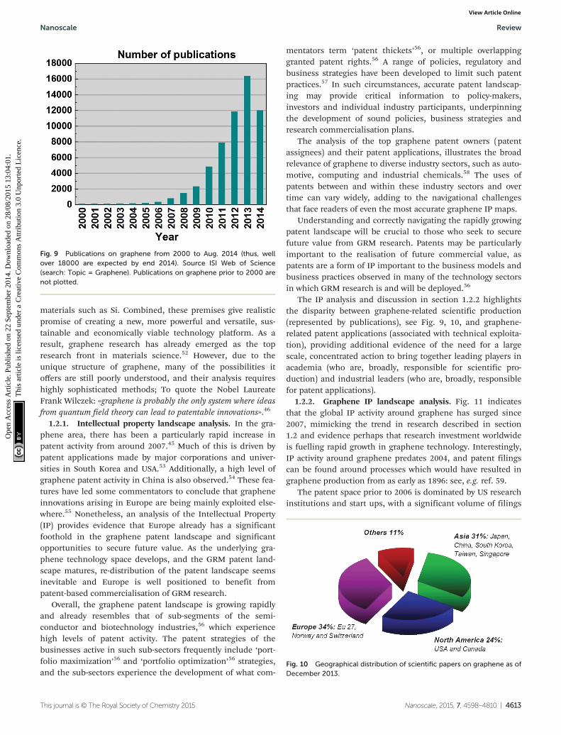
The growth of publications on GRMs is shown in Fig. 9,with no sign of slowing down. The reasons for the growth ofresearch on GRMs are manifold. First, graphene is a materialwith a unique set properties. Either separately or in combi-nations, these can be exploited in many areas of research andapplications; new possibilities are being recognized all thetime as the science of GRMs progresses. Second, grapheneScience and Technology (ST) relies on one of the most abun-dant materials on earth,51 carbon. It is an inherently sustain-able and economical technology. Thirdly, graphene is a planarmaterial and, as such, compatible with the established pro-duction technologies in ICT, and integrable with conventional
Review Nanoscale
4612 | Nanoscale, 2015, 7, 4598–4810 This journal is © The Royal Society of Chemistry 2015
Ope
n A
cces
s A
rtic
le. P
ublis
hed
on 2
2 Se
ptem
ber
2014
. Dow
nloa
ded
on 2
8/08
/201
5 13
:04:
01.
Thi
s ar
ticle
is li
cens
ed u
nder
a C
reat
ive
Com
mon
s A
ttrib
utio
n 3.
0 U
npor
ted
Lic
ence
.View Article Online
materials such as Si. Combined, these premises give realisticpromise of creating a new, more powerful and versatile, sus-tainable and economically viable technology platform. As aresult, graphene research has already emerged as the topresearch front in materials science.52 However, due to theunique structure of graphene, many of the possibilities itoffers are still poorly understood, and their analysis requireshighly sophisticated methods; To quote the Nobel LaureateFrank Wilczek: «graphene is probably the only system where ideasfrom quantum field theory can lead to patentable innovations».46
1.2.1. Intellectual property landscape analysis. In the gra-phene area, there has been a particularly rapid increase inpatent activity from around 2007.45 Much of this is driven bypatent applications made by major corporations and univer-sities in South Korea and USA.53 Additionally, a high level ofgraphene patent activity in China is also observed.54 These fea-tures have led some commentators to conclude that grapheneinnovations arising in Europe are being mainly exploited else-where.55 Nonetheless, an analysis of the Intellectual Property(IP) provides evidence that Europe already has a significantfoothold in the graphene patent landscape and significantopportunities to secure future value. As the underlying gra-phene technology space develops, and the GRM patent land-scape matures, re-distribution of the patent landscape seemsinevitable and Europe is well positioned to benefit frompatent-based commercialisation of GRM research.
Overall, the graphene patent landscape is growing rapidlyand already resembles that of sub-segments of the semi-conductor and biotechnology industries,56 which experiencehigh levels of patent activity. The patent strategies of thebusinesses active in such sub-sectors frequently include ‘port-folio maximization’56 and ‘portfolio optimization’56 strategies,and the sub-sectors experience the development of what com-
mentators term ‘patent thickets’56, or multiple overlappinggranted patent rights.56 A range of policies, regulatory andbusiness strategies have been developed to limit such patentpractices.57 In such circumstances, accurate patent landscap-ing may provide critical information to policy-makers,investors and individual industry participants, underpinningthe development of sound policies, business strategies andresearch commercialisation plans.
The analysis of the top graphene patent owners (patentassignees) and their patent applications, illustrates the broadrelevance of graphene to diverse industry sectors, such as auto-motive, computing and industrial chemicals.58 The uses ofpatents between and within these industry sectors and overtime can vary widely, adding to the navigational challengesthat face readers of even the most accurate graphene IP maps.
Understanding and correctly navigating the rapidly growingpatent landscape will be crucial to those who seek to securefuture value from GRM research. Patents may be particularlyimportant to the realisation of future commercial value, aspatents are a form of IP important to the business models andbusiness practices observed in many of the technology sectorsin which GRM research is and will be deployed.56
The IP analysis and discussion in section 1.2.2 highlightsthe disparity between graphene-related scientific production(represented by publications), see Fig. 9, 10, and graphene-related patent applications (associated with technical exploita-tion), providing additional evidence of the need for a largescale, concentrated action to bring together leading players inacademia (who are, broadly, responsible for scientific pro-duction) and industrial leaders (who are, broadly, responsiblefor patent applications).
1.2.2. Graphene IP landscape analysis. Fig. 11 indicatesthat the global IP activity around graphene has surged since2007, mimicking the trend in research described in section1.2 and evidence perhaps that research investment worldwideis fuelling rapid growth in graphene technology. Interestingly,IP activity around graphene predates 2004, and patent filingscan be found around processes which would have resulted ingraphene production from as early as 1896: see, e.g. ref. 59.
The patent space prior to 2006 is dominated by US researchinstitutions and start ups, with a significant volume of filings
Fig. 9 Publications on graphene from 2000 to Aug. 2014 (thus, wellover 18000 are expected by end 2014). Source ISI Web of Science(search: Topic = Graphene). Publications on graphene prior to 2000 arenot plotted.
Fig. 10 Geographical distribution of scientific papers on graphene as ofDecember 2013.
Nanoscale Review
This journal is © The Royal Society of Chemistry 2015 Nanoscale, 2015, 7, 4598–4810 | 4613
Ope
n A
cces
s A
rtic
le. P
ublis
hed
on 2
2 Se
ptem
ber
2014
. Dow
nloa
ded
on 2
8/08
/201
5 13
:04:
01.
Thi
s ar
ticle
is li
cens
ed u
nder
a C
reat
ive
Com
mon
s A
ttrib
utio
n 3.
0 U
npor
ted
Lic
ence
.View Article Online
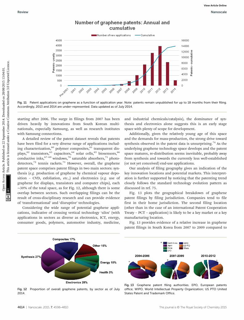
starting after 2006. The surge in filings from 2007 has beendriven heavily by innovations from South Korean multi-nationals, especially Samsung, as well as research instituteswith Samsung connections.
A detailed review of the patent dataset reveals that patentshave been filed for a very diverse range of applications includ-ing characterization,60 polymer composites,61 transparent dis-plays,62 transistors,63 capacitors,64 solar cells,65 biosensors,66
conductive inks,67–69 windows,70 saturable absorbers,71 photo-detectors,72 tennis rackets.73 However, overall, the graphenepatent space comprises patent filings in two main sectors: syn-thesis (e.g. production of graphene by chemical vapour depo-sition – CVD, exfoliation, etc.,) and electronics (e.g. use ofgraphene for displays, transistors and computer chips), each∼30% of the total space, as for Fig. 12, although there is someoverlap between sectors. Such overlapping filings can be theresult of cross-disciplinary research and can provide evidenceof ‘transformational’ and ‘disruptive’ technologies.
Considering the wide range of potential graphene appli-cations, indicative of crossing vertical technology ‘silos’ (withapplications in sectors as diverse as electronics, ICT, energy,consumer goods, polymers, automotive industry, medicine,
and industrial chemicals/catalysis), the dominance of syn-thesis and electronics alone suggests this is an early stagespace with plenty of scope for development.
Additionally, given the relatively young age of this spaceand the demands for mass-production, the strong drive towardsynthesis observed in the patent data is unsurprising.74 As theunderlying graphene technology space develops and the patentspace matures, re-distribution seems inevitable, probably awayfrom synthesis and towards the currently less well-established(or not yet conceived) end-use applications.
Our analysis of filing geography gives an indication of thekey innovation locations and potential markets. This interpret-ation is further supported by noticing that the patenting trendclosely follows the standard technology evolution pattern asdiscussed in ref. 75.
Fig. 13 plots the geographical breakdown of graphenepatent filings by filing jurisdiction. Companies tend to filefirst in their home jurisdiction. The second filing location(other than in the case of an international Patent CooperationTreaty – PCT – application) is likely to be a key market or a keymanufacturing location.
Fig. 13 provides evidence of a relative increase in graphenepatent filings in South Korea from 2007 to 2009 compared to
Fig. 11 Patent applications on graphene as a function of application year. Note: patents remain unpublished for up to 18 months from their filing.Accordingly, 2013 and 2014 are under-represented. Data updated as of July 2014.
Fig. 12 Proportion of overall graphene patents, by sector as of July2014.
Fig. 13 Graphene patent filing authorities. EPO, European patentsoffice; WIPO, World Intellectual Property Organization; US PTO UnitedStates Patent and Trademark Office.
Review Nanoscale
4614 | Nanoscale, 2015, 7, 4598–4810 This journal is © The Royal Society of Chemistry 2015
Ope
n A
cces
s A
rtic
le. P
ublis
hed
on 2
2 Se
ptem
ber
2014
. Dow
nloa
ded
on 2
8/08
/201
5 13
:04:
01.
Thi
s ar
ticle
is li
cens
ed u
nder
a C
reat
ive
Com
mon
s A
ttrib
utio
n 3.
0 U
npor
ted
Lic
ence
.View Article Online
2004–2006. This could indicate increased commercial interestin graphene technology from around 2007. The period 2010 to2012 shows a marked relative increase in graphene patentfilings in China. It should be noted that a general increase inChinese patent filings across many ST domains in this periodis observed.76 Notwithstanding this general increase inChinese patent activity, there does appear to be increased com-mercial interest in graphene in China. It is notable that theEuropean Patent Office contribution as a percentage of all gra-phene patent filings globally falls from a 8% in the period2007 to 2009 to 4% in the period 2010 to 2012.
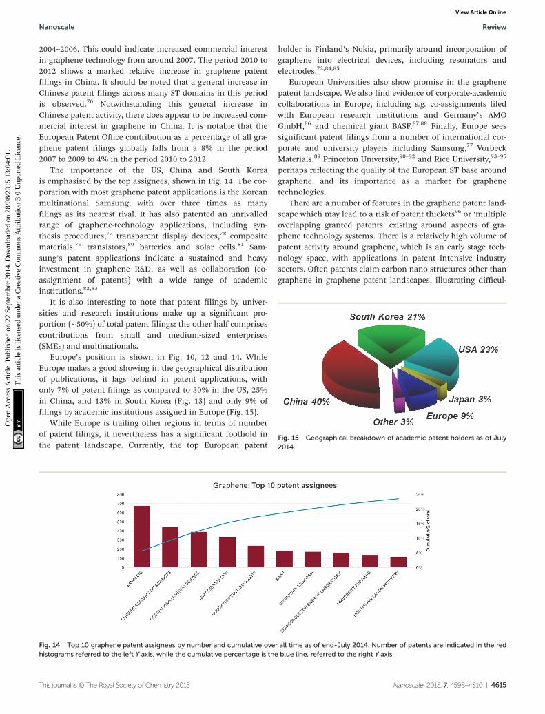
The importance of the US, China and South Koreais emphasised by the top assignees, shown in Fig. 14. The cor-poration with most graphene patent applications is the Koreanmultinational Samsung, with over three times as manyfilings as its nearest rival. It has also patented an unrivalledrange of graphene-technology applications, including syn-thesis procedures,77 transparent display devices,78 compositematerials,79 transistors,80 batteries and solar cells.81 Sam-sung’s patent applications indicate a sustained and heavyinvestment in graphene R&D, as well as collaboration (co-assignment of patents) with a wide range of academicinstitutions.82,83
It is also interesting to note that patent filings by univer-sities and research institutions make up a significant pro-portion (∼50%) of total patent filings: the other half comprisescontributions from small and medium-sized enterprises(SMEs) and multinationals.
Europe’s position is shown in Fig. 10, 12 and 14. WhileEurope makes a good showing in the geographical distributionof publications, it lags behind in patent applications, withonly 7% of patent filings as compared to 30% in the US, 25%in China, and 13% in South Korea (Fig. 13) and only 9% offilings by academic institutions assigned in Europe (Fig. 15).
While Europe is trailing other regions in terms of numberof patent filings, it nevertheless has a significant foothold inthe patent landscape. Currently, the top European patent
holder is Finland’s Nokia, primarily around incorporation ofgraphene into electrical devices, including resonators andelectrodes.72,84,85
European Universities also show promise in the graphenepatent landscape. We also find evidence of corporate-academiccollaborations in Europe, including e.g. co-assignments filedwith European research institutions and Germany’s AMOGmbH,86 and chemical giant BASF.87,88 Finally, Europe seessignificant patent filings from a number of international cor-porate and university players including Samsung,77 VorbeckMaterials,89 Princeton University,90–92 and Rice University,93–95
perhaps reflecting the quality of the European ST base aroundgraphene, and its importance as a market for graphenetechnologies.
There are a number of features in the graphene patent land-scape which may lead to a risk of patent thickets96 or ‘multipleoverlapping granted patents’ existing around aspects of gra-phene technology systems. There is a relatively high volume ofpatent activity around graphene, which is an early stage tech-nology space, with applications in patent intensive industrysectors. Often patents claim carbon nano structures other thangraphene in graphene patent landscapes, illustrating difficul-
Fig. 15 Geographical breakdown of academic patent holders as of July2014.
Fig. 14 Top 10 graphene patent assignees by number and cumulative over all time as of end-July 2014. Number of patents are indicated in the redhistograms referred to the left Y axis, while the cumulative percentage is the blue line, referred to the right Y axis.
Nanoscale Review
This journal is © The Royal Society of Chemistry 2015 Nanoscale, 2015, 7, 4598–4810 | 4615
Ope
n A
cces
s A
rtic
le. P
ublis
hed
on 2
2 Se
ptem
ber
2014
. Dow
nloa
ded
on 2
8/08
/201
5 13
:04:
01.
Thi
s ar
ticle
is li
cens
ed u
nder
a C
reat
ive
Com
mon
s A
ttrib
utio
n 3.
0 U
npor
ted
Lic
ence
.View Article Online
ties around defining ‘graphene’ and mapping the graphenepatent landscape. Additionally, the graphene patent nomen-clature is not entirely settled. Different patent examiners mightgrant patents over the same components which the differentexperts and industry players call by different names. Use of avariety of names for the same components could be a deliber-ate attempt at obfuscation. There is some support for this viewin the relevant academic literature. E.g., ref. 97 suggested thatwhere patent assessment quality is low (e.g. due to inadequateexpertise by patent examiners of a particular technologyspace), leading players might engage in high-volume patentingto deliberately create a ‘patent thicket’, with a range of possiblenegative effects on innovation.98
Despite the challenges described above, there are a numberof important opportunities of which academics, SMEs andmultinationals should take advantage, including increasedoccurrences of academia-industry collaboration (following thelead of South Korea and the US); preparing for the inevitablere-distribution of the graphene patent space as it matures and,most likely, moves away from synthesis, towards the currentlyless well-established (or not yet conceived) end-useapplications.
2. Fundamental research
One of the reasons for the fast progress of graphene researchis the wealth of its unique properties. However, what makes itreally special, and gives it a disruptive value, is that all thoseproperties are combined in a single material. Transparency–conductivity–elasticity can find use in flexible electronics, highmobility (μ)-ultimate thinness in efficient transistors for RFapplications, while transparency–impermeability–conductivitycan be exploited for transparent protective coatings. The list ofsuch combinations is ever growing. The most important areprobably those not yet explored, as they might lead to newapplications.
Currently, several record high characteristics have beenachieved with graphene, some of them reaching theoreticallypredicted limits: room temperature (RT) μ of 2.5 × 105 cm2 V−1
s−1 (ref. 99) and μ ∼ 6 × 106 cm2 V−1 s−1 at 4 K,100 a Youngmodulus of 1 TPa and intrinsic strength of 130 GPa;18 imper-meability for gases101 and so on. Graphene also has recordhigh thermal conductivity κ (∼2000 to 5300 W m−1 K−1 (ref.102) and can withstand high current densities (million timeshigher than copper).103
The surge in graphene research also paved the way forexperiments on many other 2d crystals.5 One can use similarstrategies to graphene to get new materials by mechanical5 andliquid phase exfoliation of LMs38 or CVD. An alternative strat-egy to create new 2d crystals is to start with existing ones (e.g.graphene) and use them as atomic scaffolding for modificationby chemical means (graphane33 or fluorographene34). Theresulting pool of 2d crystals is huge, and covers a range of pro-perties: from the most insulating to the best conductors, fromthe strongest to the softest. Suitable properties may be used
depending on the targeted application. E.g., to cover a range ofvarious conductance properties (but keeping the strength) onemight use combinations of graphene and fluorographene, thelatter being insulating, but almost as strong as the former.
For the long-term future, opportunities can be envisioned,combining conducting graphene with semiconducting andoptically active 2d crystals, to create hybrid multilayer super-structures. If 2d crystals hold a wide variety of properties, thesandwiched structures of 2, 3, 4… layers of such materials canfurther offer longer term prospectives. By assembling 2d struc-tures, one can engineer artificial 3d crystals, displaying tai-lored properties. Since such 2d based heterostructures104,105
can be assembled with atomic precision and individual layersof very different identity can be combined together, the pro-perties could in principle be tuned to fit any application. Fur-thermore, the functionality of those stacks is embedded in thedesign of such heterostructures. First proof of principledevices are already available,106 such as vertical tunnellingtransistors106 which show promising electrical character-istics.107,108 Starting with fundamental studies, the aim is tolearn how to tune properties of such hetero- or hybrid systemsin order to target a specific functionality.
Exploiting the full potential offered by the electronic andmechanical properties of GRMs in applications requiresextensive fundamental studies. Graphene transistors andinterconnects have an opportunity to complement andextend current Si technology. One route towards the use ofgraphene transistors for logic devices relies on creating acontrollable band gap. The limited on/off current ratio (ION/IOFF) may be resolved in new transistor designs, whichexploit the modulation of the work function of graphene,109
or carrier injection from graphene into a fully-gapped semi-conductor,110 by gaining control over vertical (rather thanplanar) transport through various barriers,106 or using gra-phene as a gate, electrode, or interconnect. For the latterapplication of graphene, its electrical and thermal conduc-tivities play an important role, so that studies of those pro-perties should be intensified, especially in polycrystallineCVD-material.
Nature offers a very broad class of 2d crystals. There areseveral LMs which retain their stability in the form of mono-layer and whose properties are complementary to those of gra-phene. Transition metal oxides (TMOs) and transition metaldichalcogenides (TMDs) also have a layered structure.111
Atoms within each layer are held together by covalent bonds,while van der Waals (vdW) interactions hold the layerstogether.111 LMs include a large number of systems with inter-esting properties.111 E.g., NiTe2 and VSe2 are semi-metals,111
WS2, WSe2, MoS2, MoSe2, MoTe2, TaS2, RhTe2, PdTe2 are semi-conductors,111 h-BN, and HfS2 are insulators, NbS2, NbSe2,NbTe2, and TaSe2 are superconductors.111 Moreover, there areother LMs such as Bi2Se3, Bi2Te3 that show thermoelectric pro-perties111 and may behave as topological insulators (TIs).112
Atomic layers of these materials can be produced,5 usingmechanical or liquid-phase exfoliation, see section 4 for moredetails on production.
Review Nanoscale
4616 | Nanoscale, 2015, 7, 4598–4810 This journal is © The Royal Society of Chemistry 2015
Ope
n A
cces
s A
rtic
le. P
ublis
hed
on 2
2 Se
ptem
ber
2014
. Dow
nloa
ded
on 2
8/08
/201
5 13
:04:
01.
Thi
s ar
ticle
is li
cens
ed u
nder
a C
reat
ive
Com
mon
s A
ttrib
utio
n 3.
0 U
npor
ted
Lic
ence
.View Article Online
A wider variety of 2d materials are also being explored, suchas the graphene analogue of silicon (i.e., silicene),113,114 ger-manium (i.e., germanene),115 phosphorus (i.e., phosphor-ene)116 and tin (i.e., stanene).117,118 Another large LM class isthat comprising the MXenes.119,120 These are derived by exfo-liating the so called MAX Phases, i.e. layered, hexagonal car-bides and nitrides having the general formula: Mn+1AXn,(MAX) where n = 1 to 3, M is an early transition metal, A is anA-group (mostly IIIA and IVA, or groups 13 and 14) elementand X is either carbon and/or nitrogen.
Chemical modification of graphene33 allows the creation ofanother class of 2d crystals with a non-zero bandgap, such asgraphane33 and fluorographene.34 Modification of thesematerials is interesting, e.g. p-doped graphane could be anelectron–phonon superconductor121 with a critical temperature(Tc) above 77 K.121
There is also a growing number of graphane analogues,such as germanane,122 and stanane.123 Ref. 122 synthesizedmm-scale crystals of hydrogen-terminated germanane fromthe topochemical deintercalation (i.e., selective for a specificchemical element) of CaGe2 resulting in a lattice of Ge atomswith an analogous geometry to the sp3-hybridized graphanesurface, in which every Ge atom is terminated with either H orOH above or below the layer.124 Germanane is thermally stableup to 75 °C.122 Above this T, dehydrogenation and amorphiza-tion begin to occur.122
2.1. Electronic transport
Graphene’s promise to complement or even replace semi-conductors in micro- and nanoelectronics is determined byseveral factors. These include its 2d nature, enabling easy pro-cessing and direct control of the charge carriers, fast moving(quasi-relativistic) electronic excitations yielding a high μ
(almost equal between electrons and holes) – both at RT andlow T, and high κ. Graphene crystals have two well-establishedallotropes, single layer graphene (SLG), where charge carriersresemble relativistic Dirac particles,125 and bilayer graphene(BLG), where electrons also have some Dirac-like properties,but have a parabolic dispersion.125 However, unlike SLG,where the absence of a gap is protected by the high symmetryof the honeycomb lattice, BLG is more versatile: a transverseelectric field can open a gap126–128 and its low-energy bandstructure can be qualitatively changed by strain.129 Each ofthese has advantages and disadvantages for a given appli-cation, and one has to learn how to control and exploit themto create functional devices.
Concerning μ, further research is needed to understand theeffects of defects and charge inhomogeneities, as well as devel-opment of doping techniques. The influence of various dielec-tric substrates or overgrown insulators also needs further basicunderstanding in order to optimize device performance.Further studies of transport regimes and optoelectronic effectsin gapped BLG are needed for FET applications. Consideringthe possible use of an electrically induced gap in BLGs forquantum dots (QDs) and engineered QDs-based circuits (e.g.,for quantum information processing130), a detailed under-
standing of the influence of disorder and Coulomb interactionon the T dependence of conductivity is required, including thenature of variable range hopping in gapped BLGs, which canbe generically described by an exponential increase of resist-ance following R ∼ exp[(T0/T )
p] (ref. 131) with T0 a constantdepending on the localization length and density of states,whereas the exponent is given by p = 1/2 for the Efros–Shklovs-kii mechanism132 and p = 1/3 for the Mott hopping regime;131
the dominating regime depending on the material.133
Besides the studies of sample-average graphene parameters,such as, Rs, it is highly desirable to get insights into localproperties of graphene used in devices. This can be achievedby means of several non-destructive techniques: Ramanspectroscopy,134–136 Kelvin probe microscopy,137 local compres-sibility measurements,138 and non-contact conductivity, usingcapacitive coupling of a probe operated at high frequency.139
The application of such techniques to graphene is natural, dueto its 2d nature. These techniques can be used to study GRMsto reveal the role of inhomogeneity in carrier density, the roleof particular substrates, and can shed light on the role of struc-tural defects and adsorbents in limiting device performance.
The peculiar properties of electrons in SLG (their similarityto relativistic Dirac particles) make a p–n junction in graphenetransparent to electrons arriving at normal incidence.140,141 Onone hand, this effect, known as Klein tunneling,141 makes itdifficult to achieve a complete pinch-off of electric current,without chemical modification or patterning.142 On the otherhand, it offers a unique possibility to create ballistic devicesand circuits where electrons experience focusing by one orseveral p–n interfaces.143 The development of such devicesrequires techniques of non-invasive gating [see, e.g., ref. 144].Another method to improve quality of graphene is to suspendit over electrodes (also used as support) and then clean it bycurrent annealing.144,145 This enables one to achieve highlyhomogeneous carrier density, and micron-long mean freepaths, enabling a detailed investigation of electronic propertiesat very low excitation energies.145
Understanding the transport properties of graphene alsoincludes its behaviour in the presence of a strong – quantising– magnetic field. As a truly 2d electron system, graphene dis-plays the fundamental phenomenon of quantum Hall effect(QHE),146–150 which consists in the precise quantisation ofHall resistance of the device.150 Both integer and several frac-tional QHE (FQHE) states have been observed,151,146,148 thelatter requiring very high crystalline quality and purematerial,151 where the Coulomb interactions between electronscan become very strong, leading to the formation of correlatedstates of matter.152 The QHE robustness in SLG opens a possi-bility to explore one, up to now, impossible regime ofquantum transport in solid-state materials: the interplaybetween QHE and superconductivity in one hybrid devicemade of graphene and a superconductor with a high criticalmagnetic field (e.g., a NbTi alloy153). Moreover, the particularrobustness of QHE in graphene on the Si face of SiC154 (stillwaiting for a complete understanding155) makes it a suitableplatform for a new type of resistance standard.154
Nanoscale Review
This journal is © The Royal Society of Chemistry 2015 Nanoscale, 2015, 7, 4598–4810 | 4617
Ope
n A
cces
s A
rtic
le. P
ublis
hed
on 2
2 Se
ptem
ber
2014
. Dow
nloa
ded
on 2
8/08
/201
5 13
:04:
01.
Thi
s ar
ticle
is li
cens
ed u
nder
a C
reat
ive
Com
mon
s A
ttrib
utio
n 3.
0 U
npor
ted
Lic
ence
.View Article Online
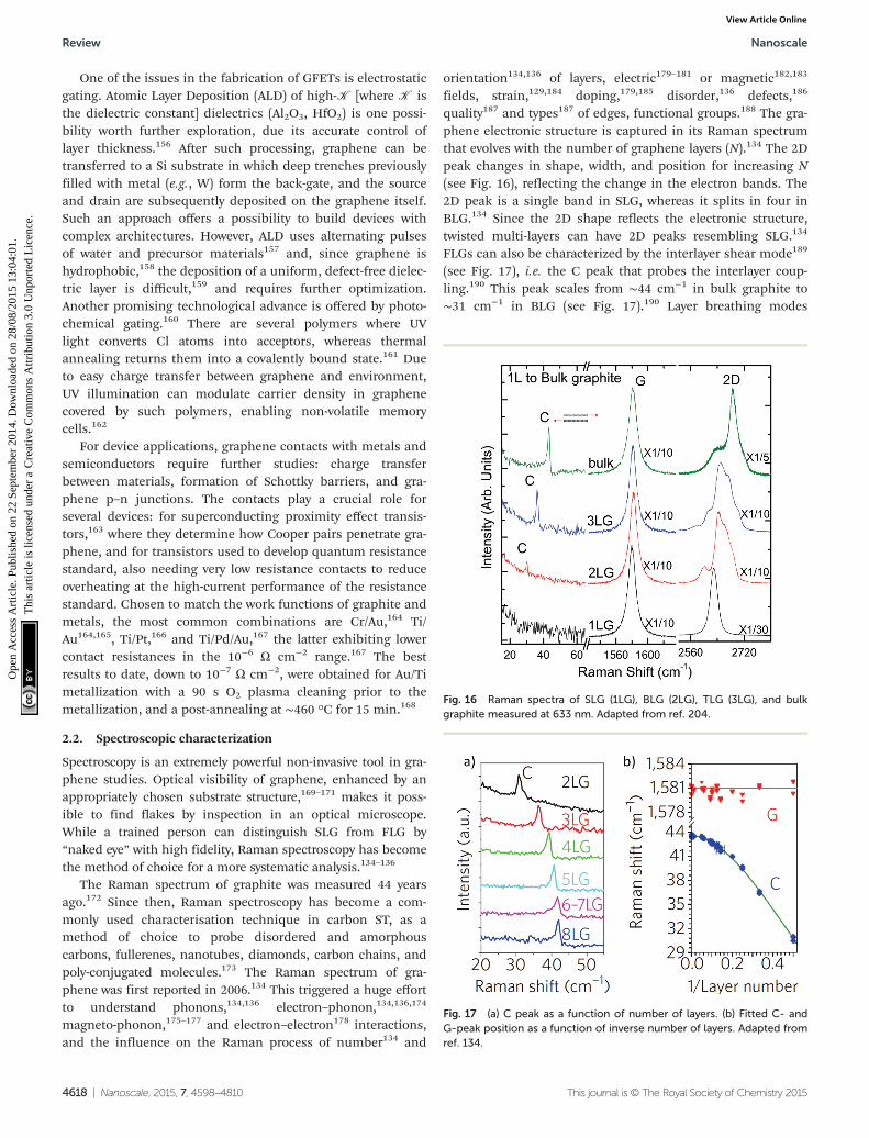
One of the issues in the fabrication of GFETs is electrostaticgating. Atomic Layer Deposition (ALD) of high-K [where K isthe dielectric constant] dielectrics (Al2O3, HfO2) is one possi-bility worth further exploration, due its accurate control oflayer thickness.156 After such processing, graphene can betransferred to a Si substrate in which deep trenches previouslyfilled with metal (e.g., W) form the back-gate, and the sourceand drain are subsequently deposited on the graphene itself.Such an approach offers a possibility to build devices withcomplex architectures. However, ALD uses alternating pulsesof water and precursor materials157 and, since graphene ishydrophobic,158 the deposition of a uniform, defect-free dielec-tric layer is difficult,159 and requires further optimization.Another promising technological advance is offered by photo-chemical gating.160 There are several polymers where UVlight converts Cl atoms into acceptors, whereas thermalannealing returns them into a covalently bound state.161 Dueto easy charge transfer between graphene and environment,UV illumination can modulate carrier density in graphenecovered by such polymers, enabling non-volatile memorycells.162
For device applications, graphene contacts with metals andsemiconductors require further studies: charge transferbetween materials, formation of Schottky barriers, and gra-phene p–n junctions. The contacts play a crucial role forseveral devices: for superconducting proximity effect transis-tors,163 where they determine how Cooper pairs penetrate gra-phene, and for transistors used to develop quantum resistancestandard, also needing very low resistance contacts to reduceoverheating at the high-current performance of the resistancestandard. Chosen to match the work functions of graphite andmetals, the most common combinations are Cr/Au,164 Ti/Au164,165, Ti/Pt,166 and Ti/Pd/Au,167 the latter exhibiting lowercontact resistances in the 10−6 Ω cm−2 range.167 The bestresults to date, down to 10−7 Ω cm−2, were obtained for Au/Timetallization with a 90 s O2 plasma cleaning prior to themetallization, and a post-annealing at ∼460 °C for 15 min.168
2.2. Spectroscopic characterization
Spectroscopy is an extremely powerful non-invasive tool in gra-phene studies. Optical visibility of graphene, enhanced by anappropriately chosen substrate structure,169–171 makes it poss-ible to find flakes by inspection in an optical microscope.While a trained person can distinguish SLG from FLG by“naked eye” with high fidelity, Raman spectroscopy has becomethe method of choice for a more systematic analysis.134–136
The Raman spectrum of graphite was measured 44 yearsago.172 Since then, Raman spectroscopy has become a com-monly used characterisation technique in carbon ST, as amethod of choice to probe disordered and amorphouscarbons, fullerenes, nanotubes, diamonds, carbon chains, andpoly-conjugated molecules.173 The Raman spectrum of gra-phene was first reported in 2006.134 This triggered a huge effortto understand phonons,134,136 electron–phonon,134,136,174
magneto-phonon,175–177 and electron–electron178 interactions,and the influence on the Raman process of number134 and
orientation134,136 of layers, electric179–181 or magnetic182,183
fields, strain,129,184 doping,179,185 disorder,136 defects,186
quality187 and types187 of edges, functional groups.188 The gra-phene electronic structure is captured in its Raman spectrumthat evolves with the number of graphene layers (N).134 The 2Dpeak changes in shape, width, and position for increasing N(see Fig. 16), reflecting the change in the electron bands. The2D peak is a single band in SLG, whereas it splits in four inBLG.134 Since the 2D shape reflects the electronic structure,twisted multi-layers can have 2D peaks resembling SLG.134
FLGs can also be characterized by the interlayer shear mode189
(see Fig. 17), i.e. the C peak that probes the interlayer coup-ling.190 This peak scales from ∼44 cm−1 in bulk graphite to∼31 cm−1 in BLG (see Fig. 17).190 Layer breathing modes
Fig. 16 Raman spectra of SLG (1LG), BLG (2LG), TLG (3LG), and bulkgraphite measured at 633 nm. Adapted from ref. 204.
Fig. 17 (a) C peak as a function of number of layers. (b) Fitted C- andG-peak position as a function of inverse number of layers. Adapted fromref. 134.
Review Nanoscale
4618 | Nanoscale, 2015, 7, 4598–4810 This journal is © The Royal Society of Chemistry 2015
Ope
n A
cces
s A
rtic
le. P
ublis
hed
on 2
2 Se
ptem
ber
2014
. Dow
nloa
ded
on 2
8/08
/201
5 13
:04:
01.
Thi
s ar
ticle
is li
cens
ed u
nder
a C
reat
ive
Com
mon
s A
ttrib
utio
n 3.
0 U
npor
ted
Lic
ence
.View Article Online
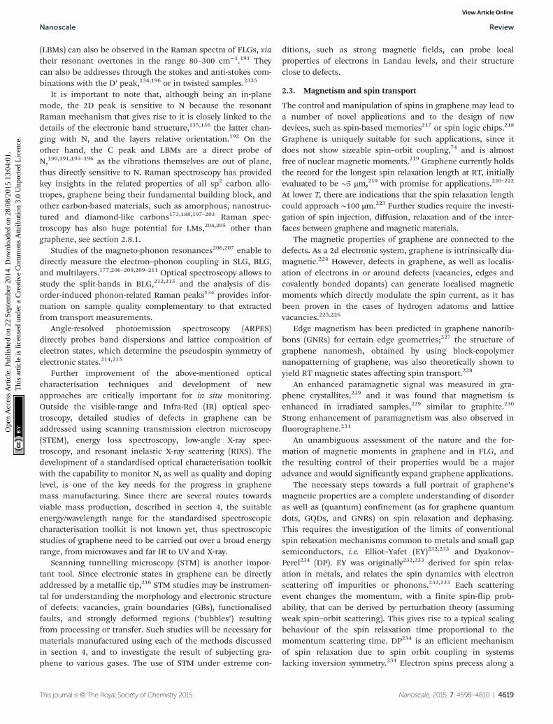
(LBMs) can also be observed in the Raman spectra of FLGs, viatheir resonant overtones in the range 80–300 cm−1.191 Theycan also be addresses through the stokes and anti-stokes com-binations with the D’ peak,134,196 or in twisted samples.2335
It is important to note that, although being an in-planemode, the 2D peak is sensitive to N because the resonantRaman mechanism that gives rise to it is closely linked to thedetails of the electronic band structure,135,136 the latter chan-ging with N, and the layers relative orientation.192 On theother hand, the C peak and LBMs are a direct probe ofN,190,191,193–196 as the vibrations themselves are out of plane,thus directly sensitive to N. Raman spectroscopy has providedkey insights in the related properties of all sp2 carbon allo-tropes, graphene being their fundamental building block, andother carbon-based materials, such as amorphous, nanostruc-tured and diamond-like carbons173,188,197–203 Raman spec-troscopy has also huge potential for LMs,204,205 other thangraphene, see section 2.8.1.
Studies of the magneto-phonon resonances206,207 enable todirectly measure the electron–phonon coupling in SLG, BLG,and multilayers.177,206–208,209–211 Optical spectroscopy allows tostudy the split-bands in BLG,212,213 and the analysis of dis-order-induced phonon-related Raman peaks134 provides infor-mation on sample quality complementary to that extractedfrom transport measurements.
Angle-resolved photoemission spectroscopy (ARPES)directly probes band dispersions and lattice composition ofelectron states, which determine the pseudospin symmetry ofelectronic states.214,215
Further improvement of the above-mentioned opticalcharacterisation techniques and development of newapproaches are critically important for in situ monitoring.Outside the visible-range and Infra-Red (IR) optical spec-troscopy, detailed studies of defects in graphene can beaddressed using scanning transmission electron microscopy(STEM), energy loss spectroscopy, low-angle X-ray spec-troscopy, and resonant inelastic X-ray scattering (RIXS). Thedevelopment of a standardised optical characterisation toolkitwith the capability to monitor N, as well as quality and dopinglevel, is one of the key needs for the progress in graphenemass manufacturing. Since there are several routes towardsviable mass production, described in section 4, the suitableenergy/wavelength range for the standardised spectroscopiccharacterisation toolkit is not known yet, thus spectroscopicstudies of graphene need to be carried out over a broad energyrange, from microwaves and far IR to UV and X-ray.
Scanning tunnelling microscopy (STM) is another impor-tant tool. Since electronic states in graphene can be directlyaddressed by a metallic tip,216 STM studies may be instrumen-tal for understanding the morphology and electronic structureof defects: vacancies, grain boundaries (GBs), functionalisedfaults, and strongly deformed regions (‘bubbles’) resultingfrom processing or transfer. Such studies will be necessary formaterials manufactured using each of the methods discussedin section 4, and to investigate the result of subjecting gra-phene to various gases. The use of STM under extreme con-
ditions, such as strong magnetic fields, can probe localproperties of electrons in Landau levels, and their structureclose to defects.
2.3. Magnetism and spin transport
The control and manipulation of spins in graphene may lead toa number of novel applications and to the design of newdevices, such as spin-based memories217 or spin logic chips.218
Graphene is uniquely suitable for such applications, since itdoes not show sizeable spin–orbit coupling,74 and is almostfree of nuclear magnetic moments.219 Graphene currently holdsthe record for the longest spin relaxation length at RT, initiallyevaluated to be ∼5 μm,219 with promise for applications.220–222
At lower T, there are indications that the spin relaxation lengthcould approach ∼100 μm.223 Further studies require the investi-gation of spin injection, diffusion, relaxation and of the inter-faces between graphene and magnetic materials.
The magnetic properties of graphene are connected to thedefects. As a 2d electronic system, graphene is intrinsically dia-magnetic.224 However, defects in graphene, as well as localis-ation of electrons in or around defects (vacancies, edges andcovalently bonded dopants) can generate localised magneticmoments which directly modulate the spin current, as it hasbeen proven in the cases of hydrogen adatoms and latticevacancies.225,226
Edge magnetism has been predicted in graphene nanorib-bons (GNRs) for certain edge geometries;227 the structure ofgraphene nanomesh, obtained by using block-copolymernanopatterning of graphene, was also theoretically shown toyield RT magnetic states affecting spin transport.228
An enhanced paramagnetic signal was measured in gra-phene crystallites,229 and it was found that magnetism isenhanced in irradiated samples,229 similar to graphite.230
Strong enhancement of paramagnetism was also observed influorographene.231
An unambiguous assessment of the nature and the for-mation of magnetic moments in graphene and in FLG, andthe resulting control of their properties would be a majoradvance and would significantly expand graphene applications.
The necessary steps towards a full portrait of graphene’smagnetic properties are a complete understanding of disorderas well as (quantum) confinement (as for graphene quantumdots, GQDs, and GNRs) on spin relaxation and dephasing.This requires the investigation of the limits of conventionalspin relaxation mechanisms common to metals and small gapsemiconductors, i.e. Elliot–Yafet (EY)232,233 and Dyakonov–Perel234 (DP). EY was originally232,233 derived for spin relax-ation in metals, and relates the spin dynamics with electronscattering off impurities or phonons.232,233 Each scatteringevent changes the momentum, with a finite spin-flip prob-ability, that can be derived by perturbation theory (assumingweak spin–orbit scattering). This gives rise to a typical scalingbehaviour of the spin relaxation time proportional to themomentum scattering time. DP234 is an efficient mechanismof spin relaxation due to spin orbit coupling in systemslacking inversion symmetry.234 Electron spins precess along a
Nanoscale Review
This journal is © The Royal Society of Chemistry 2015 Nanoscale, 2015, 7, 4598–4810 | 4619
Ope
n A
cces
s A
rtic
le. P
ublis
hed
on 2
2 Se
ptem
ber
2014
. Dow
nloa
ded
on 2
8/08
/201
5 13
:04:
01.
Thi
s ar
ticle
is li
cens
ed u
nder
a C
reat
ive
Com
mon
s A
ttrib
utio
n 3.
0 U
npor
ted
Lic
ence
.View Article Online
magnetic field which depends on the momentum.234 At eachscattering event, the direction and frequency of the precessionchange randomly. The scaling behaviour is opposite to EY,with a spin relaxation time which is inversely proportional tothe momentum scattering time.235
Two other mechanisms of spin relaxation in graphene havebeen proposed.236,237 One involves local magnetic momentswhich produce resonances and fast spin relaxation based onthe resonant scattering of electrons off magnetic moments,which can be due to nonmagnetic adatoms, organic mole-cules, or vacancies.236 The other is related to the interplaybetween spin and pseudospin quantum degrees of freedomwhen disorder does not mix valleys.237 Such strong contri-bution of spin/pseudospin entanglement is particularly impor-tant when defects or impurities at the origin of local Rashbaspin–orbit coupling (i.e. a momentum-dependent splitting ofspin bands in 2d systems)238 preserve the pseudospin sym-metry and lead to very long mean free path.
The role of edges on spin scattering and relaxation has yetto be clarified, as well as the case when the injected spin-polar-ized charges flow in close proximity (and interact) with otherextrinsic spins (in localized or more extended charged states,located below or on top of the graphene).
The role of the substrate, contacts and environmental con-ditions on spin relaxation needs to be clarified. A detailedcomparison between exfoliated graphene on SiO2, graphene onBN, and graphene grown on SiC is still missing. This wouldallow the classification of materials and devices’ parameters,which have, to date, shown limited spin transport. Theseresults could be compared with spin transport and relaxationin suspended graphene devices, which would provide the refer-ence clean system. This is of fundamental importance forfurther exploration of more complex uses of the spin degree offreedom inside technology.
A systematic comparison of spintronic systems based onSLG, BLG and FLG still needs to be carried out. With a focuson spin ensembles, the RT capability of graphene devices hasto be ascertained.
The knowledge derived from these investigations could beexploited in multiple ways. E.g., novel studies could be carriedout to induce (para-) magnetism by introducing localiseddefect states in a controlled way, or by decoration of thesurface with magnetic atoms or molecules. In the search forfingerprints of local magnetic ordering states and magneto-resistance profiles, chemically modified graphene (CMG)-based materials should be produced to investigate the poten-tial of new physical phenomena. Other topics include studyingelectronic transport in graphene in proximity of ferromagneticmaterials or ferromagnetic insulators (magnetic oxides asEuO, EuS, high-Curie T (above which the magnetic state of thesystem is lost) Yttrium Iron Garnet (YIG), NiO, CoFe2O4). Thismay induce spin polarization, which could be exploited todemonstrate spin filtering effects.239 Related issues focus onthe existence of nanomagnetism of magnetic materials de-posited on graphene, and the understanding of the interfacialelectronic structure of such contacts.
2.4. Polycrystalline graphene
The GB role in transport and optical properties240 needs to befully investigated, especially in view of large-scale production.The theoretical exploration of the properties of large size rea-listic models is crucial for guiding experiments.
Microscopic studies of grain boundaries are needed todetermine their precise lattice structure and morphology, aswell as the related functionalization of broken carbon bondsby atoms/molecules acquired from environment. Grain bound-aries in the 2d graphene lattice are topological line-defectsconsisting of non-hexagonal carbon rings, as evidenced byaberration corrected high resolution TEM investigations.241
Although they are expected to substantially alter the electronicproperties of the unperturbed graphene lattice,242 so far littleexperimental insight into the underlying mechanisms is avail-able. GB introduce tension in graphene nanocrystals,243
which, in turn, bears influence on the electronic properties,including local doping. From the point of view of electronictransport, GB generate scattering, possibly with a strongly non-linear behaviour, but present knowledge on the precise effectsis incomplete. Ref. 244 suggested a scaling behaviour of poly-crystalline graphene,244 which gives μ ∼ 300 000 cm2 V−1 s−1 atRT for an average grain size of 1 μm and clean GB. This alsoshows the need for a more detailed GB chemical characteriz-ation, since these are more chemically reactive and could drivean essential part of the resistance of the material. Indeed, e.g.,CVD grown samples fall behind by about an order of magni-tude compared to mechanically exfoliated ones.9 The internalGB structure, and the resulting broken electron-hole (e–h) andinversion symmetry may generate thermo-power245 and localrectification,246 which may affect high current performance.Depending on their structure, GBs have been initially theoreti-cally predicted to be highly transparent,247 or perfectly reflec-tive,247 while other studies suggest GB act as molecular metallicwires248 or filter propagating carriers based on valley-index.249
A comprehensive picture of GBs’ spectral properties is thusmissing, and should be established using STM and atomicforce microscopy (AFM), and local optical probes,250 givenpossible specific light absorption and emission,251,252 The useof graphene for energy applications, in solar cells, also requiresunderstanding of the GB role in the charge transfer betweengraphene and environment. Moreover, optics, combined withelectrochemistry, is needed to figure out ways to re-crystallizegraphene poly-crystals, and to assess durability (i.e. until whenthe (opto)electronic and thermal properties are maintainedwithout degradation). There is growing evidence that GBsdegrade the electronic performance.253,254
2.5. Thermal and mechanical properties of graphene
Practical implementation of graphene requires the under-standing of its performance in real devices, as well as its dura-bility under ambient and extreme conditions. A specialisedeffort will be needed to study the reliability of graphene-baseddevices, such as electric or thermal stress tests, device lifetime,etc. To preserve performance, it is likely that some protection
Review Nanoscale
4620 | Nanoscale, 2015, 7, 4598–4810 This journal is © The Royal Society of Chemistry 2015
Ope
n A
cces
s A
rtic
le. P
ublis
hed
on 2
2 Se
ptem
ber
2014
. Dow
nloa
ded
on 2
8/08
/201
5 13
:04:
01.
Thi
s ar
ticle
is li
cens
ed u
nder
a C
reat
ive
Com
mon
s A
ttrib
utio
n 3.
0 U
npor
ted
Lic
ence
.View Article Online

of the graphene and the metals will be needed to minimizeenvironmental effects.
Due to the sp2 hybridization, pristine SLG is very strong,and it takes 48 000 kN m kg−1 of specific strength (i.e. strength(force per unit area at failure) divided by density) before break-ing18 (compare this to steel’s 154 kN m kg−1 (ref. 255)). Thismakes graphene a desirable addition to lightweight polymers,and the enforcer of their mechanical properties. Moreover, asultrathin stretchable membrane, SLG is an ideal material fornonlinear tuneable electromechanical systems. However, forthe practical implementation of realistic graphene systems, adetailed study of mechanical properties of polycrystalline gra-phene is needed in vacuum, ambient environment, and of gra-phene embedded in polymers. Studies of mechanicalproperties of GBs between graphene nano-crystals will requirea further improvement of scanning techniques. The durabilityof graphene in various systems will also depend on its abilityto recrystallize upon interaction with various chemical agents,as well under various types of radiation, from UV and softX-rays to cosmic rays.
The application of graphene in the electronics and opto-electronics requires detailed understanding of its thermal andmechanical properties. Several early experiments,256,257 indi-cate that graphene is a very good heat conductor, due to thehigh speed of acoustic phonons in its tight and lightweightlattice. Detailed studies of heat transfer through graphene andthe interfacial Kapitza thermal resistance258 (i.e. the measureof an interface’s resistance to thermal flow) between grapheneand other materials (metallic contacts, insulating substrates,polymer matrix) are needed. Graphene performance at high
current may lead to overheating, and quantitative studies(both experimental and theoretical) are needed to compare itsperformance with the standards set in electronics industry.Moreover, overheating upon current annealing may lead to itsdestruction, so that studies of thermal and thermo-mechanicalproperties are needed to assess its durability in devices, andoptimise its use in realistic and extreme conditions. In particu-lar, in situ studies of kinetics and dynamics at the break point(use of HRTEM would be appropriate) are a challenging butnecessary step towards practical implementation.
Experimental studies need to be complemented by ab initioand multiscale modelling of nanomechanical and heat trans-port properties, and modelling of graphene at strong non-equi-librium conditions (see Section 2.10.4).
2.6. Artificial graphene structures in condensed-mattersystems
Advances in the design and fabrication of artificial honeycomblattices or artificial graphene (AG) pave the way for the realiz-ation, investigation, and manipulation of a wide class ofsystems displaying massless Dirac quasiparticles, topologicalphases, and strong correlations. Such artificial structures arecurrently created by three approaches: atom-by-atom assem-bling by scanning probe methods,259 nanopatterning of ultra-high- μ two-dimensional electron gases (2DEGs) in semi-conductors,260 and optical trapping of ultracold atoms incrystals of light.261 Examples of AG structures realized so farare shown in Fig. 18. The interplay between single-particleband-structure-engineering,262 cooperative effects and dis-
Fig. 18 (a) SEM image of AG structure realized by e-beam lithography and reactive ion etching on a GaAs/AlGaAs heterostructure. Electrons localizeunderneath the nanopillars (white dots; also shown in (d).260 (b) STM topography of a molecular graphene lattice composed of 149 carbon monoxidemolecules.259 (c) A honeycomb optical lattice for ultracold K atoms.261 (e) Electron moving under the prescription of the relativistic Dirac equation.The light blue line shows a quasi-classical path of one such electron as it enters the AG lattice made of carbon monoxide molecules (black/redatoms) positioned individually by an STM tip (comprised of Ir atoms, dark blue). (f ) Tight-binding calculations of the Dirac Fermion miniband struc-ture of the AGs in (a) and (d).
Nanoscale Review
This journal is © The Royal Society of Chemistry 2015 Nanoscale, 2015, 7, 4598–4810 | 4621
Ope
n A
cces
s A
rtic
le. P
ublis
hed
on 2
2 Se
ptem
ber
2014
. Dow
nloa
ded
on 2
8/08
/201
5 13
:04:
01.
Thi
s ar
ticle
is li
cens
ed u
nder
a C
reat
ive
Com
mon
s A
ttrib
utio
n 3.
0 U
npor
ted
Lic
ence
.View Article Online
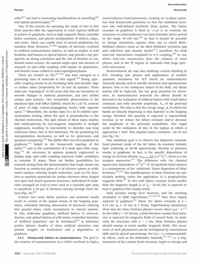
order263 can lead to interesting manifestations in tunnelling264
and optical spectroscopies.262
One of the reasons for pursuing the study of AGs is thatthese systems offer the opportunity to reach regimes difficultto achieve in graphene, such as high magnetic fluxes, tuneablelattice constants, and precise manipulation of defects, edges,and strain. These can enable tests of several predictions formassless Dirac fermions,265,266 Studies of electrons confinedin artificial semiconductor lattices, as well as studies of coldfermions and bosons in optical lattices, may provide a key per-spective on strong correlation and the role of disorder in con-densed matter science. AG systems might open new avenues ofresearch on spin–orbit coupling, with impact on spintronics,and frontier issues related to novel topological phases.
These are centred on TIs,267–269 that have emerged as apromising class of materials in this regard.269 Strong spin–orbit coupling results in an insulating bulk and metallic edgeor surface states (respectively for 2d and 3d systems). Thesestates are “topological” in the sense that they are insensitive tosmooth changes in material parameters, and also exhibitunique spin textures. One remarkable phenomenon is theQuantum Spin Hall Effect (QSHE), which for a 2d TI, consistsof pairs of edge counter-propagating modes with oppositespins.112 Meanwhile, the surface state of a 3d TI exhibits spin-momentum locking, where the spin is perpendicular to theelectron momentum. The spin texture of these states impliesthat backscattering by non-magnetic impurities is stronglysuppressed, resulting in insensitivity to disorder and longcoherence times. Due to this behaviour, TIs are promising fornext-generation electronics, as well as for spintronics andquantum computing.270 The QSHE effect was first predicted ingraphene,112 linked to the honeycomb topology of thelattice112 and to the contribution of a weak spin–orbit coup-ling.112 AG structures in systems properly engineered todisplay large spin–orbit coupling represent viable candidatesto simulate TI states. There are further possibilities forresearch arising from the demonstration that single atoms canfunction as atomic-size gates of a 2d electron system at noblemetal surfaces, whereby simple molecules, such as CO, func-tion as repulsive potentials for surface electrons when shapedinto open and closed quantum structures. Individual CO mole-cules arranged on Cu(111) were used as a tuneable gate arrayto transform a 2d gas of electrons moving through these lat-tices (Fig. 18).201
Control over every lattice position and potential wouldresult in control of the spatial texture of the hopping para-meter, ultimately allowing observation of electronic orderinginto ground states, rarely encountered in natural systems.In AGs, molecular graphene, artificial lattices in semicon-ductors, and optical lattices of cold atoms, controlled densitiesof ‘artificial impurities’ can be introduced259 in otherwiseperfect lattices. Studies of these artificial structures mayprovide insights on localization and μ degradation ingraphene.
2.6.1. Honeycomb lattices in semiconductors. The goal isthe creation of nanostructures on a 2DEG confined in high-μ
semiconductor heterostructures, creating an in-plane poten-tial with honeycomb geometry so that the miniband struc-ture has well-defined (isolated) Dirac points. The latticeconstant in graphene is fixed at ∼1.42 Å. In contrast, AGstructures in semiconductors can have tuneable lattice periodin the range 10–100 nm,260 so that it should be possibleto change interaction regimes from one in which Mott–Hubbard physics (such as the Mott–Hubbard excitation gapand collection spin density modes271) manifests for weakinter-site interactions compared to π–π coupling,260 to onewhere inter-site interactions drive the creation of novelphases, and to the TI regime in materials with large spin–orbit interaction.
Semiconductor AG may also challenge current thinking inICT, revealing new physics and applications of scalablequantum simulators for ICT based on semiconductormaterials already used in real-life electronic and optoelectronicdevices. Due to the embryonic nature of the field, any futureactivity will be high-risk, but has great potential for discov-eries. In semiconductor materials the efforts should bedirected to the realization of artificial lattices with small latticeconstants and with tuneable amplitude, V0, of the potentialmodulation. The idea is that the energy range, Δ, in which thebands are linearly dispersing in AGs depends on the hoppingenergy, therefore this quantity is expected to exponentiallyincrease as we reduce the lattice constant and/or decreasethe amplitude of the potential modulation. One targetcould be the realization of AGs in the regime in which Δ
approaches 1 meV. This requires lattice constants ∼20–40 nm(see Fig. 19).
One ambitious goal is to observe the dispersive intrasub-band plasmon mode of the AG lattice by resonant inelasticlight scattering or far-IR spectroscopy. Peculiar to plasmonmodes in graphene, in fact, is the specific dependence ofenergy on electron density: ωplasmon(q) ∝ n1/4q1/2, where q is thein-plane wavevector.272 The difference with the classicalsquare-root dependence n1/2q1/2 of 2d parabolic-band systemsis a consequence of the ‘relativistic’ linear dispersion of Diracfermions,273,274 The manifestations of Dirac fermions are par-ticularly striking under the application of a perpendicularmagnetic field.275 In AGs with lattice constant much smallerthan the magnetic length (a ≪ lB = ħc/eB) this is expected tolead to graphene-like Landau levels.
Such peculiar energy level structure, and the resultinganomalies in QHE experiments,145,146,148 have been largelyexplored in graphene276 where the lattice constant is a =0.14 nm (lB ≈ 25 nm at 1 Tesla). Tight-binding calculationsshow that the Dirac Fermion physics occurs when lB/a > 1.275
In AGs with a ∼ 10–20 nm, a Dirac-Fermion Landau level struc-ture is expected for magnetic fields of several Tesla. In mole-cular AG structures with a ∼ 1 nm, Dirac Fermion physicsshould emerge at much smaller magnetic fields. The occur-rence of such phenomena can be investigated by conventionalQHE and by optical spectroscopy. For lB/a < 1, commensurabil-ity effects, such as the Hofstadter butterfly,277–279 i.e. a frag-mentation of the Landau levels structure, begin to emerge and
Review Nanoscale
4622 | Nanoscale, 2015, 7, 4598–4810 This journal is © The Royal Society of Chemistry 2015
Ope
n A
cces
s A
rtic
le. P
ublis
hed
on 2
2 Se
ptem
ber
2014
. Dow
nloa
ded
on 2
8/08
/201
5 13
:04:
01.
Thi
s ar
ticle
is li
cens
ed u
nder
a C
reat
ive
Com
mon
s A
ttrib
utio
n 3.
0 U
npor
ted
Lic
ence
.View Article Online
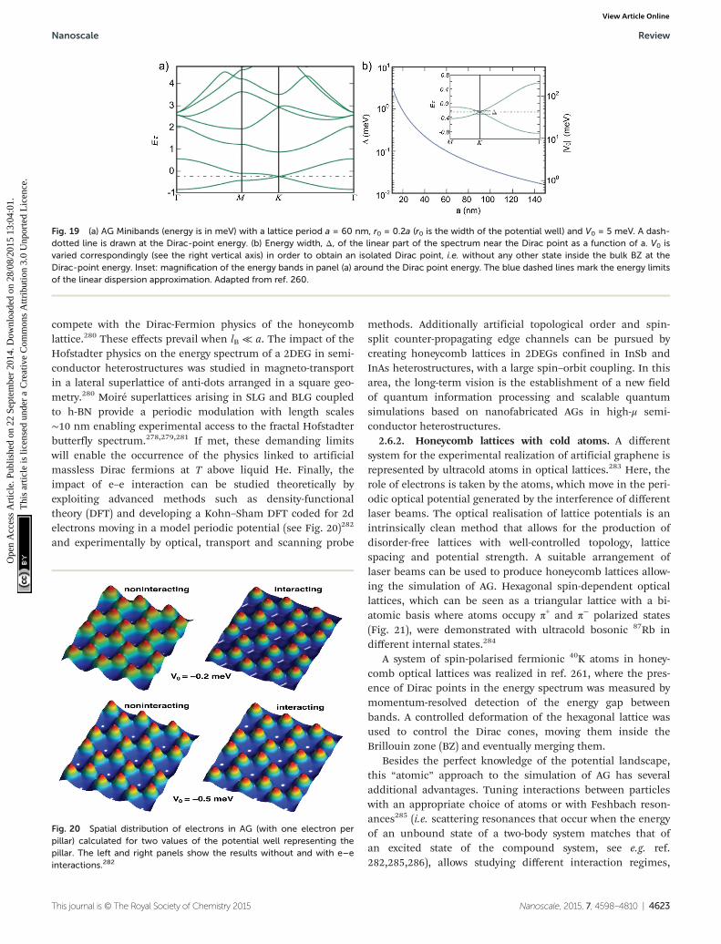
compete with the Dirac-Fermion physics of the honeycomblattice.280 These effects prevail when lB ≪ a. The impact of theHofstadter physics on the energy spectrum of a 2DEG in semi-conductor heterostructures was studied in magneto-transportin a lateral superlattice of anti-dots arranged in a square geo-metry.280 Moiré superlattices arising in SLG and BLG coupledto h-BN provide a periodic modulation with length scales∼10 nm enabling experimental access to the fractal Hofstadterbutterfly spectrum.278,279,281 If met, these demanding limitswill enable the occurrence of the physics linked to artificialmassless Dirac fermions at T above liquid He. Finally, theimpact of e–e interaction can be studied theoretically byexploiting advanced methods such as density-functionaltheory (DFT) and developing a Kohn–Sham DFT coded for 2delectrons moving in a model periodic potential (see Fig. 20)282
and experimentally by optical, transport and scanning probe
methods. Additionally artificial topological order and spin-split counter-propagating edge channels can be pursued bycreating honeycomb lattices in 2DEGs confined in InSb andInAs heterostructures, with a large spin–orbit coupling. In thisarea, the long-term vision is the establishment of a new fieldof quantum information processing and scalable quantumsimulations based on nanofabricated AGs in high-μ semi-conductor heterostructures.
2.6.2. Honeycomb lattices with cold atoms. A differentsystem for the experimental realization of artificial graphene isrepresented by ultracold atoms in optical lattices.283 Here, therole of electrons is taken by the atoms, which move in the peri-odic optical potential generated by the interference of differentlaser beams. The optical realisation of lattice potentials is anintrinsically clean method that allows for the production ofdisorder-free lattices with well-controlled topology, latticespacing and potential strength. A suitable arrangement oflaser beams can be used to produce honeycomb lattices allow-ing the simulation of AG. Hexagonal spin-dependent opticallattices, which can be seen as a triangular lattice with a bi-atomic basis where atoms occupy π+ and π− polarized states(Fig. 21), were demonstrated with ultracold bosonic 87Rb indifferent internal states.284
A system of spin-polarised fermionic 40K atoms in honey-comb optical lattices was realized in ref. 261, where the pres-ence of Dirac points in the energy spectrum was measured bymomentum-resolved detection of the energy gap betweenbands. A controlled deformation of the hexagonal lattice wasused to control the Dirac cones, moving them inside theBrillouin zone (BZ) and eventually merging them.
Besides the perfect knowledge of the potential landscape,this “atomic” approach to the simulation of AG has severaladditional advantages. Tuning interactions between particleswith an appropriate choice of atoms or with Feshbach reson-ances285 (i.e. scattering resonances that occur when the energyof an unbound state of a two-body system matches that ofan excited state of the compound system, see e.g. ref.282,285,286), allows studying different interaction regimes,
Fig. 19 (a) AG Minibands (energy is in meV) with a lattice period a = 60 nm, r0 = 0.2a (r0 is the width of the potential well) and V0 = 5 meV. A dash-dotted line is drawn at the Dirac-point energy. (b) Energy width, Δ, of the linear part of the spectrum near the Dirac point as a function of a. V0 isvaried correspondingly (see the right vertical axis) in order to obtain an isolated Dirac point, i.e. without any other state inside the bulk BZ at theDirac-point energy. Inset: magnification of the energy bands in panel (a) around the Dirac point energy. The blue dashed lines mark the energy limitsof the linear dispersion approximation. Adapted from ref. 260.
Fig. 20 Spatial distribution of electrons in AG (with one electron perpillar) calculated for two values of the potential well representing thepillar. The left and right panels show the results without and with e–einteractions.282
Nanoscale Review
This journal is © The Royal Society of Chemistry 2015 Nanoscale, 2015, 7, 4598–4810 | 4623
Ope
n A
cces
s A
rtic
le. P
ublis
hed
on 2
2 Se
ptem
ber
2014
. Dow
nloa
ded
on 2
8/08
/201
5 13
:04:
01.
Thi
s ar
ticle
is li
cens
ed u
nder
a C
reat
ive
Com
mon
s A
ttrib
utio
n 3.
0 U
npor
ted
Lic
ence
.View Article Online

from ideal Dirac Fermion physics to strongly-interactingMott–Hubbard physics. Multi-layer systems can be producedwith an additional optical lattice in the orthogonal direction tothe 2d honeycomb plane, with an adjustable tunnel couplingbetween the layers, which could allow the investigation of arti-ficial BLG/FLG. Other interesting perspectives arise from theintroduction of artificial magnetic fields for effectively-chargedneutral atoms and spin–orbit coupling, which enrich the pos-sibilities of Hamiltonian engineering in ultracold atomicsystems.266
Several detection techniques can be used to probe the pro-perties of atomic AG, including measuring transport of atomsacross the lattice, even with single-atom (electron) imagingresolution. The excitation spectrum of the system can bedirectly measured with inelastic light scattering (Bragg spec-troscopy),287 which gives access to the dynamical structurefactor, while correlation functions of different order (1st order:phase correlations, 2nd order: density–density correlations) canbe probed in time-of-flight experiments.286
In addition, a unique feature of ultracold atom experimentsis the possibility of changing the lattice and interaction para-meters from one experiment to the other, and even modifyingthem in real time, inducing rapid changes in the AG Hamil-tonian enabling the investigation of non-equilibriumdynamics, which can give important information on thesystem properties.
Of particular relevance is the possibility to study the impactof disorder, which can be introduced in a controlled way byusing additional inhomogeneous optical potentials, createde.g. with optical speckles or multi-chromatic optical lattices,288
see Fig. 22. This allows the investigation of the interplaybetween disorder and Dirac Fermion physics. An examplerelated to 1d optical lattices is shown in Fig. 23, where thedifferent images show the size of an ultracold cloud of non-interacting 39K Bose-condensed atoms for different evolution
Fig. 21 (a) Lattice potential with alternating π+ (green spheres) and π− (red spheres) polarization. The upper plot shows a cut through the 2d poten-tial. (b) 1d potential along the channel of the orange dashed line in (a) for particles in different Zeeman states.284
Fig. 22 Schematic depiction of ultracold atoms trapped in artificialcrystals produced by the interference of laser beams (optical lattices).
Fig. 23 Localization transition for 39 K ultracold atoms in a quasiperio-dic bichromatic lattice: as Δ is increased the atomic cloud becomesAnderson-localized.263
Review Nanoscale
4624 | Nanoscale, 2015, 7, 4598–4810 This journal is © The Royal Society of Chemistry 2015
Ope
n A
cces
s A
rtic
le. P
ublis
hed
on 2
2 Se
ptem
ber
2014
. Dow
nloa
ded
on 2
8/08
/201
5 13
:04:
01.
Thi
s ar
ticle
is li
cens
ed u
nder
a C
reat
ive
Com
mon
s A
ttrib
utio
n 3.
0 U
npor
ted
Lic
ence
.View Article Online
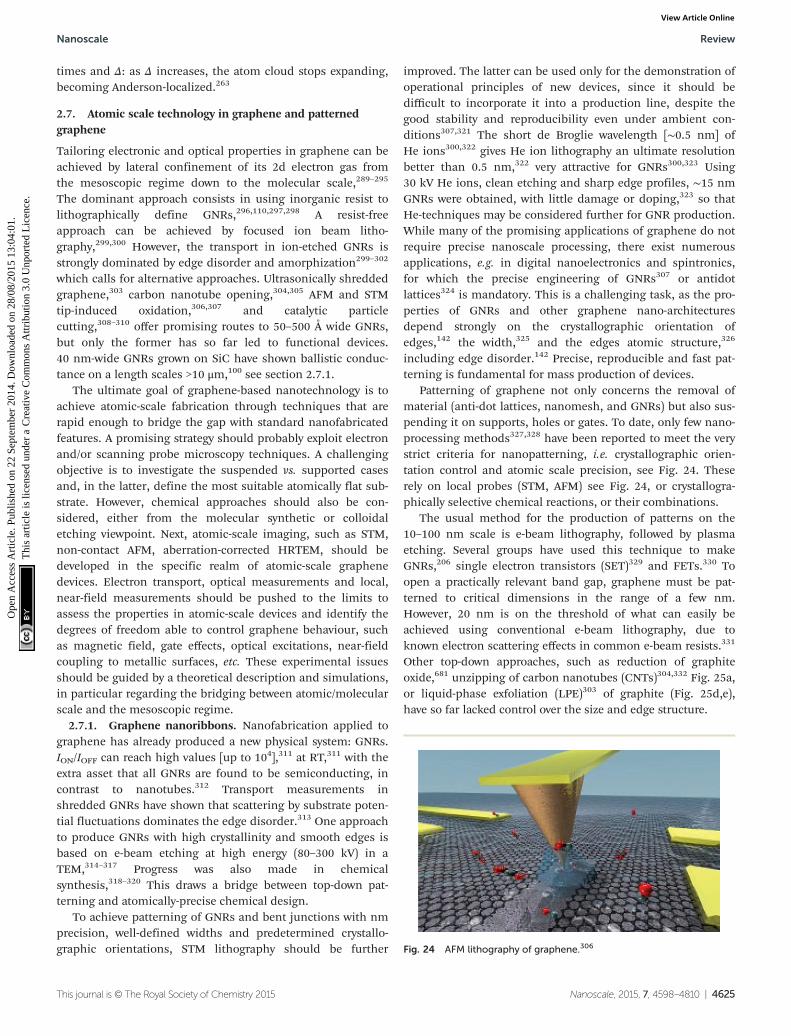
times and Δ: as Δ increases, the atom cloud stops expanding,becoming Anderson-localized.263
2.7. Atomic scale technology in graphene and patternedgraphene
Tailoring electronic and optical properties in graphene can beachieved by lateral confinement of its 2d electron gas fromthe mesoscopic regime down to the molecular scale,289–295
The dominant approach consists in using inorganic resist tolithographically define GNRs,296,110,297,298 A resist-freeapproach can be achieved by focused ion beam litho-graphy,299,300 However, the transport in ion-etched GNRs isstrongly dominated by edge disorder and amorphization299–302
which calls for alternative approaches. Ultrasonically shreddedgraphene,303 carbon nanotube opening,304,305 AFM and STMtip-induced oxidation,306,307 and catalytic particlecutting,308–310 offer promising routes to 50–500 Å wide GNRs,but only the former has so far led to functional devices.40 nm-wide GNRs grown on SiC have shown ballistic conduc-tance on a length scales >10 μm,100 see section 2.7.1.
The ultimate goal of graphene-based nanotechnology is toachieve atomic-scale fabrication through techniques that arerapid enough to bridge the gap with standard nanofabricatedfeatures. A promising strategy should probably exploit electronand/or scanning probe microscopy techniques. A challengingobjective is to investigate the suspended vs. supported casesand, in the latter, define the most suitable atomically flat sub-strate. However, chemical approaches should also be con-sidered, either from the molecular synthetic or colloidaletching viewpoint. Next, atomic-scale imaging, such as STM,non-contact AFM, aberration-corrected HRTEM, should bedeveloped in the specific realm of atomic-scale graphenedevices. Electron transport, optical measurements and local,near-field measurements should be pushed to the limits toassess the properties in atomic-scale devices and identify thedegrees of freedom able to control graphene behaviour, suchas magnetic field, gate effects, optical excitations, near-fieldcoupling to metallic surfaces, etc. These experimental issuesshould be guided by a theoretical description and simulations,in particular regarding the bridging between atomic/molecularscale and the mesoscopic regime.
2.7.1. Graphene nanoribbons. Nanofabrication applied tographene has already produced a new physical system: GNRs.ION/IOFF can reach high values [up to 104],311 at RT,311 with theextra asset that all GNRs are found to be semiconducting, incontrast to nanotubes.312 Transport measurements inshredded GNRs have shown that scattering by substrate poten-tial fluctuations dominates the edge disorder.313 One approachto produce GNRs with high crystallinity and smooth edges isbased on e-beam etching at high energy (80–300 kV) in aTEM,314–317 Progress was also made in chemicalsynthesis,318–320 This draws a bridge between top-down pat-terning and atomically-precise chemical design.
To achieve patterning of GNRs and bent junctions with nmprecision, well-defined widths and predetermined crystallo-graphic orientations, STM lithography should be further
improved. The latter can be used only for the demonstration ofoperational principles of new devices, since it should bedifficult to incorporate it into a production line, despite thegood stability and reproducibility even under ambient con-ditions307,321 The short de Broglie wavelength [∼0.5 nm] ofHe ions300,322 gives He ion lithography an ultimate resolutionbetter than 0.5 nm,322 very attractive for GNRs300,323 Using30 kV He ions, clean etching and sharp edge profiles, ∼15 nmGNRs were obtained, with little damage or doping,323 so thatHe-techniques may be considered further for GNR production.While many of the promising applications of graphene do notrequire precise nanoscale processing, there exist numerousapplications, e.g. in digital nanoelectronics and spintronics,for which the precise engineering of GNRs307 or antidotlattices324 is mandatory. This is a challenging task, as the pro-perties of GNRs and other graphene nano-architecturesdepend strongly on the crystallographic orientation ofedges,142 the width,325 and the edges atomic structure,326
including edge disorder.142 Precise, reproducible and fast pat-terning is fundamental for mass production of devices.
Patterning of graphene not only concerns the removal ofmaterial (anti-dot lattices, nanomesh, and GNRs) but also sus-pending it on supports, holes or gates. To date, only few nano-processing methods327,328 have been reported to meet the verystrict criteria for nanopatterning, i.e. crystallographic orien-tation control and atomic scale precision, see Fig. 24. Theserely on local probes (STM, AFM) see Fig. 24, or crystallogra-phically selective chemical reactions, or their combinations.
The usual method for the production of patterns on the10–100 nm scale is e-beam lithography, followed by plasmaetching. Several groups have used this technique to makeGNRs,206 single electron transistors (SET)329 and FETs.330 Toopen a practically relevant band gap, graphene must be pat-terned to critical dimensions in the range of a few nm.However, 20 nm is on the threshold of what can easily beachieved using conventional e-beam lithography, due toknown electron scattering effects in common e-beam resists.331
Other top-down approaches, such as reduction of graphiteoxide,681 unzipping of carbon nanotubes (CNTs)304,332 Fig. 25a,or liquid-phase exfoliation (LPE)303 of graphite (Fig. 25d,e),have so far lacked control over the size and edge structure.
Fig. 24 AFM lithography of graphene.306
Nanoscale Review
This journal is © The Royal Society of Chemistry 2015 Nanoscale, 2015, 7, 4598–4810 | 4625
Ope
n A
cces
s A
rtic
le. P
ublis
hed
on 2
2 Se
ptem
ber
2014
. Dow
nloa
ded
on 2
8/08
/201
5 13
:04:
01.
Thi
s ar
ticle
is li
cens
ed u
nder
a C
reat
ive
Com
mon
s A
ttrib
utio
n 3.
0 U
npor
ted
Lic
ence
.View Article Online
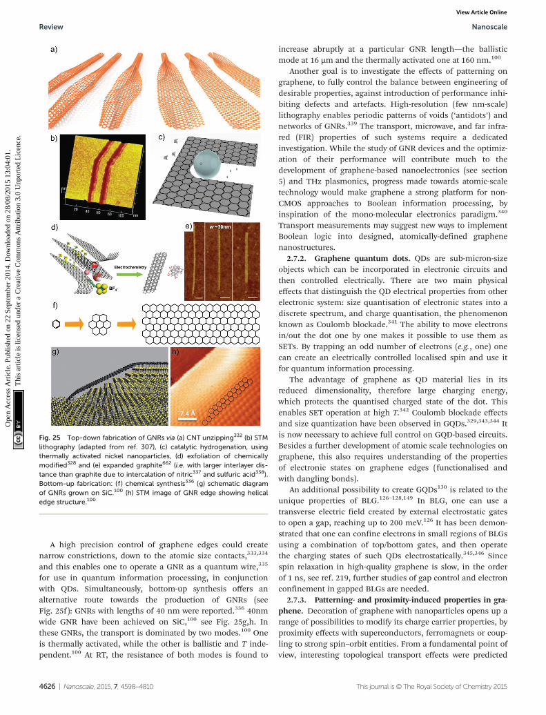
A high precision control of graphene edges could createnarrow constrictions, down to the atomic size contacts,333,334
and this enables one to operate a GNR as a quantum wire,335
for use in quantum information processing, in conjunctionwith QDs. Simultaneously, bottom-up synthesis offers analternative route towards the production of GNRs (seeFig. 25f): GNRs with lengths of 40 nm were reported.336 40nmwide GNR have been achieved on SiC,100 see Fig. 25g,h. Inthese GNRs, the transport is dominated by two modes.100 Oneis thermally activated, while the other is ballistic and T inde-pendent.100 At RT, the resistance of both modes is found to
increase abruptly at a particular GNR length—the ballisticmode at 16 µm and the thermally activated one at 160 nm.100
Another goal is to investigate the effects of patterning ongraphene, to fully control the balance between engineering ofdesirable properties, against introduction of performance inhi-biting defects and artefacts. High-resolution (few nm-scale)lithography enables periodic patterns of voids (‘antidots’) andnetworks of GNRs.339 The transport, microwave, and far infra-red (FIR) properties of such systems require a dedicatedinvestigation. While the study of GNR devices and the optimiz-ation of their performance will contribute much to thedevelopment of graphene-based nanoelectronics (see section5) and THz plasmonics, progress made towards atomic-scaletechnology would make graphene a strong platform for non-CMOS approaches to Boolean information processing, byinspiration of the mono-molecular electronics paradigm.340
Transport measurements may suggest new ways to implementBoolean logic into designed, atomically-defined graphenenanostructures.
2.7.2. Graphene quantum dots. QDs are sub-micron-sizeobjects which can be incorporated in electronic circuits andthen controlled electrically. There are two main physicaleffects that distinguish the QD electrical properties from otherelectronic system: size quantisation of electronic states into adiscrete spectrum, and charge quantisation, the phenomenonknown as Coulomb blockade.341 The ability to move electronsin/out the dot one by one makes it possible to use them asSETs. By trapping an odd number of electrons (e.g., one) onecan create an electrically controlled localised spin and use itfor quantum information processing.
The advantage of graphene as QD material lies in itsreduced dimensionality, therefore large charging energy,which protects the quantised charged state of the dot. Thisenables SET operation at high T.342 Coulomb blockade effectsand size quantization have been observed in GQDs.329,343,344 Itis now necessary to achieve full control on GQD-based circuits.Besides a further development of atomic scale technologies ongraphene, this also requires understanding of the propertiesof electronic states on graphene edges (functionalised andwith dangling bonds).
An additional possibility to create GQDs130 is related to theunique properties of BLG.126–128,149 In BLG, one can use atransverse electric field created by external electrostatic gatesto open a gap, reaching up to 200 meV.126 It has been demon-strated that one can confine electrons in small regions of BLGsusing a combination of top/bottom gates, and then operatethe charging states of such QDs electrostatically.345,346 Sincespin relaxation in high-quality graphene is slow, in the orderof 1 ns, see ref. 219, further studies of gap control and electronconfinement in gapped BLGs are needed.
2.7.3. Patterning- and proximity-induced properties in gra-phene. Decoration of graphene with nanoparticles opens up arange of possibilities to modify its charge carrier properties, byproximity effects with superconductors, ferromagnets or coup-ling to strong spin–orbit entities. From a fundamental point ofview, interesting topological transport effects were predicted
Fig. 25 Top-down fabrication of GNRs via (a) CNT unzipping332 (b) STMlithography (adapted from ref. 307), (c) catalytic hydrogenation, usingthermally activated nickel nanoparticles, (d) exfoliation of chemicallymodified328 and (e) expanded graphite662 (i.e. with larger interlayer dis-tance than graphite due to intercalation of nitric337 and sulfuric acid338).Bottom-up fabrication: (f ) chemical synthesis336 (g) schematic diagramof GNRs grown on SiC.100 (h) STM image of GNR edge showing helicaledge structure.100
Review Nanoscale
4626 | Nanoscale, 2015, 7, 4598–4810 This journal is © The Royal Society of Chemistry 2015
Ope
n A
cces
s A
rtic
le. P
ublis
hed
on 2
2 Se
ptem
ber
2014
. Dow
nloa
ded
on 2
8/08
/201
5 13
:04:
01.
Thi
s ar
ticle
is li
cens
ed u
nder
a C
reat
ive
Com
mon
s A
ttrib
utio
n 3.
0 U
npor
ted
Lic
ence
.View Article Online
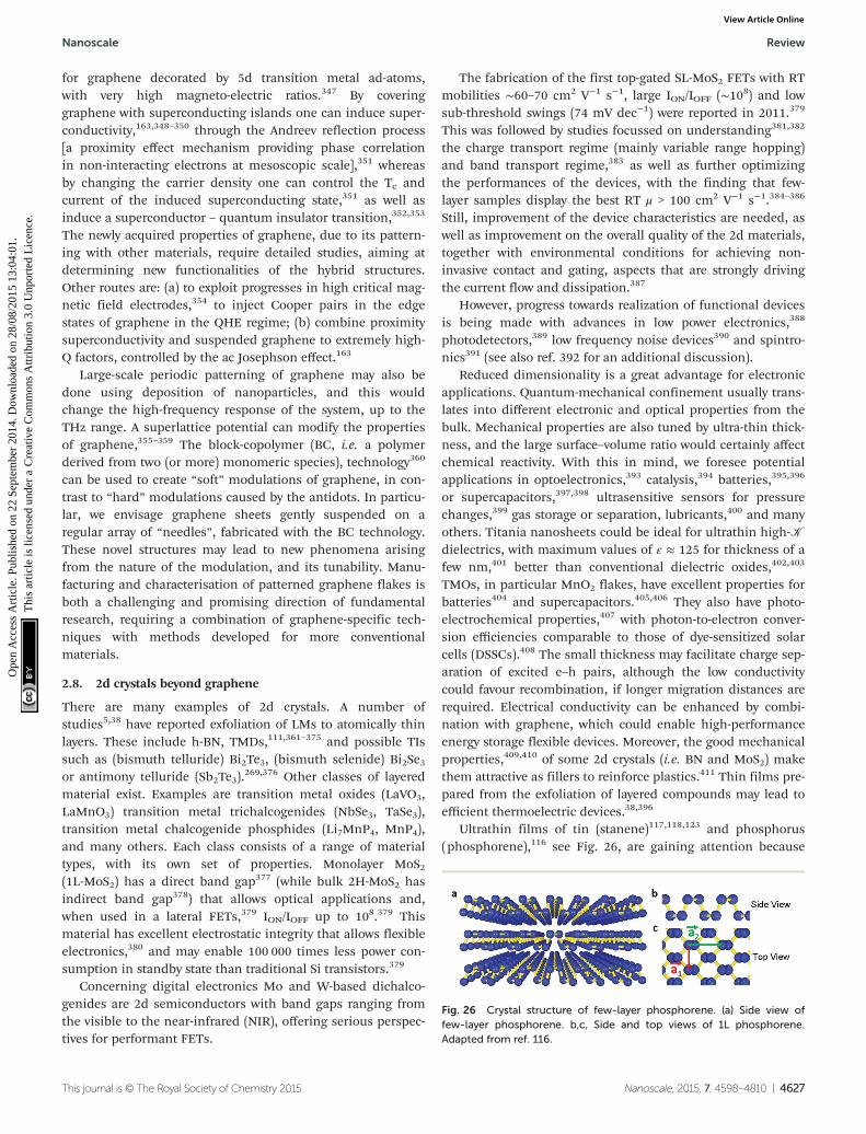
for graphene decorated by 5d transition metal ad-atoms,with very high magneto-electric ratios.347 By coveringgraphene with superconducting islands one can induce super-conductivity,163,348–350 through the Andreev reflection process[a proximity effect mechanism providing phase correlationin non-interacting electrons at mesoscopic scale],351 whereasby changing the carrier density one can control the Tc andcurrent of the induced superconducting state,351 as well asinduce a superconductor – quantum insulator transition,352,353
The newly acquired properties of graphene, due to its pattern-ing with other materials, require detailed studies, aiming atdetermining new functionalities of the hybrid structures.Other routes are: (a) to exploit progresses in high critical mag-netic field electrodes,354 to inject Cooper pairs in the edgestates of graphene in the QHE regime; (b) combine proximitysuperconductivity and suspended graphene to extremely high-Q factors, controlled by the ac Josephson effect.163
Large-scale periodic patterning of graphene may also bedone using deposition of nanoparticles, and this wouldchange the high-frequency response of the system, up to theTHz range. A superlattice potential can modify the propertiesof graphene,355–359 The block-copolymer (BC, i.e. a polymerderived from two (or more) monomeric species), technology360
can be used to create “soft” modulations of graphene, in con-trast to “hard” modulations caused by the antidots. In particu-lar, we envisage graphene sheets gently suspended on aregular array of “needles”, fabricated with the BC technology.These novel structures may lead to new phenomena arisingfrom the nature of the modulation, and its tunability. Manu-facturing and characterisation of patterned graphene flakes isboth a challenging and promising direction of fundamentalresearch, requiring a combination of graphene-specific tech-niques with methods developed for more conventionalmaterials.
2.8. 2d crystals beyond graphene
There are many examples of 2d crystals. A number ofstudies5,38 have reported exfoliation of LMs to atomically thinlayers. These include h-BN, TMDs,111,361–375 and possible TIssuch as (bismuth telluride) Bi2Te3, (bismuth selenide) Bi2Se3or antimony telluride (Sb2Te3).
269,376 Other classes of layeredmaterial exist. Examples are transition metal oxides (LaVO3,LaMnO3) transition metal trichalcogenides (NbSe3, TaSe3),transition metal chalcogenide phosphides (Li7MnP4, MnP4),and many others. Each class consists of a range of materialtypes, with its own set of properties. Monolayer MoS2(1L-MoS2) has a direct band gap377 (while bulk 2H-MoS2 hasindirect band gap378) that allows optical applications and,when used in a lateral FETs,379 ION/IOFF up to 108.379 Thismaterial has excellent electrostatic integrity that allows flexibleelectronics,380 and may enable 100 000 times less power con-sumption in standby state than traditional Si transistors.379
Concerning digital electronics Mo and W-based dichalco-genides are 2d semiconductors with band gaps ranging fromthe visible to the near-infrared (NIR), offering serious perspec-tives for performant FETs.
The fabrication of the first top-gated SL-MoS2 FETs with RTmobilities ∼60–70 cm2 V−1 s−1, large ION/IOFF (∼108) and lowsub-threshold swings (74 mV dec−1) were reported in 2011.379
This was followed by studies focussed on understanding381,382
the charge transport regime (mainly variable range hopping)and band transport regime,383 as well as further optimizingthe performances of the devices, with the finding that few-layer samples display the best RT μ > 100 cm2 V−1 s−1.384–386
Still, improvement of the device characteristics are needed, aswell as improvement on the overall quality of the 2d materials,together with environmental conditions for achieving non-invasive contact and gating, aspects that are strongly drivingthe current flow and dissipation.387
However, progress towards realization of functional devicesis being made with advances in low power electronics,388
photodetectors,389 low frequency noise devices390 and spintro-nics391 (see also ref. 392 for an additional discussion).
Reduced dimensionality is a great advantage for electronicapplications. Quantum-mechanical confinement usually trans-lates into different electronic and optical properties from thebulk. Mechanical properties are also tuned by ultra-thin thick-ness, and the large surface–volume ratio would certainly affectchemical reactivity. With this in mind, we foresee potentialapplications in optoelectronics,393 catalysis,394 batteries,395,396
or supercapacitors,397,398 ultrasensitive sensors for pressurechanges,399 gas storage or separation, lubricants,400 and manyothers. Titania nanosheets could be ideal for ultrathin high-Kdielectrics, with maximum values of ε ≈ 125 for thickness of afew nm,401 better than conventional dielectric oxides,402,403
TMOs, in particular MnO2 flakes, have excellent properties forbatteries404 and supercapacitors.405,406 They also have photo-electrochemical properties,407 with photon-to-electron conver-sion efficiencies comparable to those of dye-sensitized solarcells (DSSCs).408 The small thickness may facilitate charge sep-aration of excited e–h pairs, although the low conductivitycould favour recombination, if longer migration distances arerequired. Electrical conductivity can be enhanced by combi-nation with graphene, which could enable high-performanceenergy storage flexible devices. Moreover, the good mechanicalproperties,409,410 of some 2d crystals (i.e. BN and MoS2) makethem attractive as fillers to reinforce plastics.411 Thin films pre-pared from the exfoliation of layered compounds may lead toefficient thermoelectric devices.38,396
Ultrathin films of tin (stanene)117,118,123 and phosphorus(phosphorene),116 see Fig. 26, are gaining attention because
Fig. 26 Crystal structure of few-layer phosphorene. (a) Side view offew-layer phosphorene. b,c, Side and top views of 1L phosphorene.Adapted from ref. 116.
Nanoscale Review
This journal is © The Royal Society of Chemistry 2015 Nanoscale, 2015, 7, 4598–4810 | 4627
Ope
n A
cces
s A
rtic
le. P
ublis
hed
on 2
2 Se
ptem
ber
2014
. Dow
nloa
ded
on 2
8/08
/201
5 13
:04:
01.
Thi
s ar
ticle
is li
cens
ed u
nder
a C
reat
ive
Com
mon
s A
ttrib
utio
n 3.
0 U
npor
ted
Lic
ence
.View Article Online
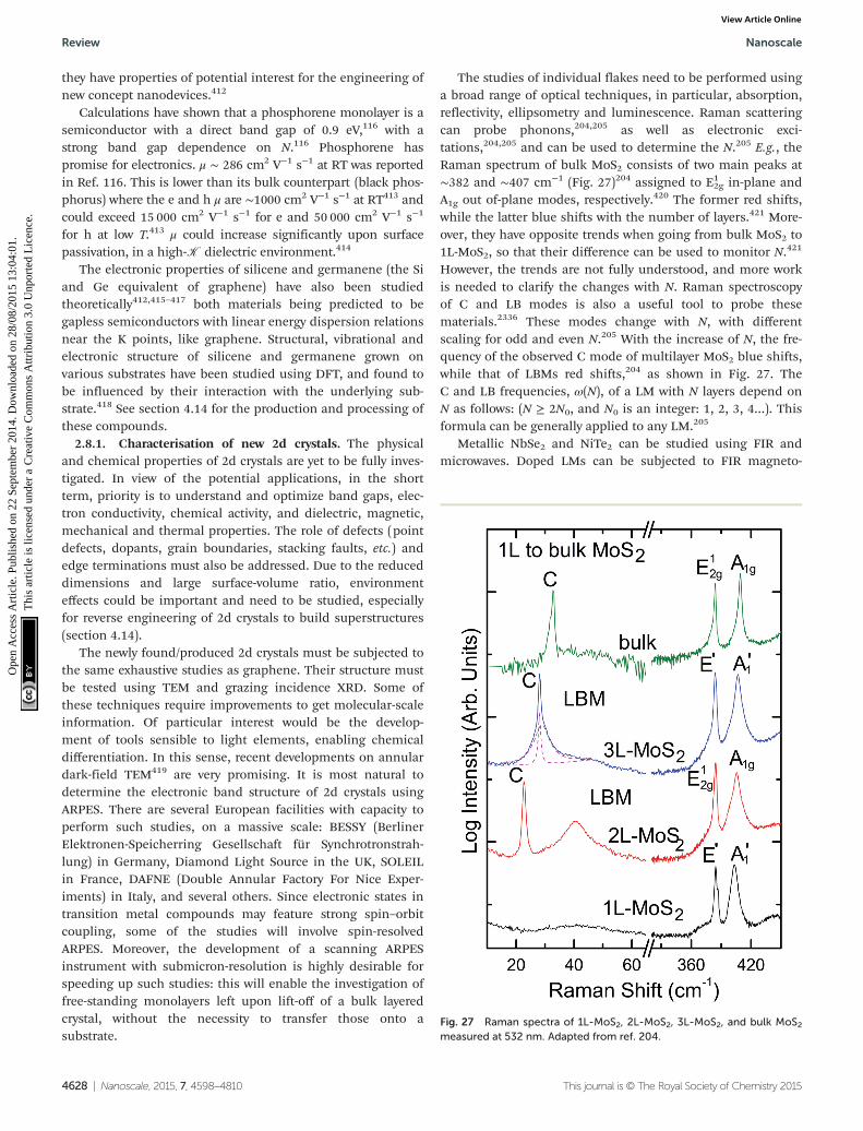
they have properties of potential interest for the engineering ofnew concept nanodevices.412
Calculations have shown that a phosphorene monolayer is asemiconductor with a direct band gap of 0.9 eV,116 with astrong band gap dependence on N.116 Phosphorene haspromise for electronics. μ ∼ 286 cm2 V−1 s−1 at RT was reportedin Ref. 116. This is lower than its bulk counterpart (black phos-phorus) where the e and h μ are ∼1000 cm2 V−1 s−1 at RT413 andcould exceed 15 000 cm2 V−1 s−1 for e and 50 000 cm2 V−1 s−1
for h at low T.413 μ could increase significantly upon surfacepassivation, in a high-K dielectric environment.414
The electronic properties of silicene and germanene (the Siand Ge equivalent of graphene) have also been studiedtheoretically412,415–417 both materials being predicted to begapless semiconductors with linear energy dispersion relationsnear the K points, like graphene. Structural, vibrational andelectronic structure of silicene and germanene grown onvarious substrates have been studied using DFT, and found tobe influenced by their interaction with the underlying sub-strate.418 See section 4.14 for the production and processing ofthese compounds.
2.8.1. Characterisation of new 2d crystals. The physicaland chemical properties of 2d crystals are yet to be fully inves-tigated. In view of the potential applications, in the shortterm, priority is to understand and optimize band gaps, elec-tron conductivity, chemical activity, and dielectric, magnetic,mechanical and thermal properties. The role of defects (pointdefects, dopants, grain boundaries, stacking faults, etc.) andedge terminations must also be addressed. Due to the reduceddimensions and large surface-volume ratio, environmenteffects could be important and need to be studied, especiallyfor reverse engineering of 2d crystals to build superstructures(section 4.14).
The newly found/produced 2d crystals must be subjected tothe same exhaustive studies as graphene. Their structure mustbe tested using TEM and grazing incidence XRD. Some ofthese techniques require improvements to get molecular-scaleinformation. Of particular interest would be the develop-ment of tools sensible to light elements, enabling chemicaldifferentiation. In this sense, recent developments on annulardark-field TEM419 are very promising. It is most natural todetermine the electronic band structure of 2d crystals usingARPES. There are several European facilities with capacity toperform such studies, on a massive scale: BESSY (BerlinerElektronen-Speicherring Gesellschaft für Synchrotronstrah-lung) in Germany, Diamond Light Source in the UK, SOLEILin France, DAFNE (Double Annular Factory For Nice Exper-iments) in Italy, and several others. Since electronic states intransition metal compounds may feature strong spin–orbitcoupling, some of the studies will involve spin-resolvedARPES. Moreover, the development of a scanning ARPESinstrument with submicron-resolution is highly desirable forspeeding up such studies: this will enable the investigation offree-standing monolayers left upon lift-off of a bulk layeredcrystal, without the necessity to transfer those onto asubstrate.
The studies of individual flakes need to be performed usinga broad range of optical techniques, in particular, absorption,reflectivity, ellipsometry and luminescence. Raman scatteringcan probe phonons,204,205 as well as electronic exci-tations,204,205 and can be used to determine the N.205 E.g., theRaman spectrum of bulk MoS2 consists of two main peaks at∼382 and ∼407 cm−1 (Fig. 27)204 assigned to E12g in-plane andA1g out of-plane modes, respectively.420 The former red shifts,while the latter blue shifts with the number of layers.421 More-over, they have opposite trends when going from bulk MoS2 to1L-MoS2, so that their difference can be used to monitor N.421
However, the trends are not fully understood, and more workis needed to clarify the changes with N. Raman spectroscopyof C and LB modes is also a useful tool to probe thesematerials.2336 These modes change with N, with differentscaling for odd and even N.205 With the increase of N, the fre-quency of the observed C mode of multilayer MoS2 blue shifts,while that of LBMs red shifts,204 as shown in Fig. 27. TheC and LB frequencies, ω(N), of a LM with N layers depend onN as follows: (N ≥ 2N0, and N0 is an integer: 1, 2, 3, 4…). Thisformula can be generally applied to any LM.205
Metallic NbSe2 and NiTe2 can be studied using FIR andmicrowaves. Doped LMs can be subjected to FIR magneto-
Fig. 27 Raman spectra of 1L-MoS2, 2L-MoS2, 3L-MoS2, and bulk MoS2measured at 532 nm. Adapted from ref. 204.
Review Nanoscale
4628 | Nanoscale, 2015, 7, 4598–4810 This journal is © The Royal Society of Chemistry 2015
Ope
n A
cces
s A
rtic
le. P
ublis
hed
on 2
2 Se
ptem
ber
2014
. Dow
nloa
ded
on 2
8/08
/201
5 13
:04:
01.
Thi
s ar
ticle
is li
cens
ed u
nder
a C
reat
ive
Com
mon
s A
ttrib
utio
n 3.
0 U
npor
ted
Lic
ence
.View Article Online
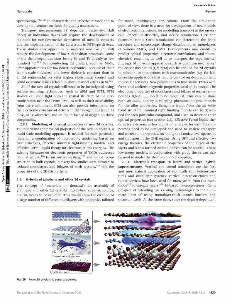
spectroscopy,422,423 to characterise the effective masses and todevelop non-contact methods for quality assessment.
Transport measurements (T dependent resistivity, Halleffect) of individual flakes will require the development ofmethods for non-destructive deposition of metallic contactsand the implementation of the 2d crystals in FET-type devices.These studies may appear to be material sensitive and willrequire the development of low-T deposition processes: someof the dichalcogenides start losing Se and Te already at fewhundred °C.424 Semiconducting 2d crystals, such as MoS2,offer opportunities for low-power electronics. Because of theiratomic-scale thickness and lower dielectric constant than inSi, 2d semiconductors offer higher electrostatic control andcould overcome issues related to short-channel effects in Si.425
All of the new 2d crystals will need to be investigated usingsurface scanning techniques, such as AFM and STM. STMstudies can shed light onto the spatial structure of the elec-tronic states near the Fermi level, as well as their accessibilityfrom the environment. STM can also provide information onthe electronic structure of defects in dichalcogenides (such asS, Se, or Te vacancies) and on the influence of oxygen on thesecompounds.
2.8.2. Modelling of physical properties of new 2d crystals.To understand the physical properties of the new 2d crystals, amulti-scale modelling approach is needed for each particularmaterial: a combination of microscopic modelling based onfirst principles, effective minimal tight-binding models, andeffective Fermi liquid theory for electrons at low energies. Theexisting literature on electronic properties of TMDs addressesband structure,426 Fermi surface nesting,427 and lattice recon-struction in bulk crystals, but very few studies were devoted toisolated monolayers and bilayers of such crystals,428 and theproperties of the 2DEGs in them.
2.9. Hybrids of graphene and other 2d crystals
The concept of “materials on demand”: an assembly ofgraphene and other 2d crystals into hybrid super-structures,Fig. 28, needs to be explored. This would allow the creation ofa large number of different multilayers with properties tailored
for novel, multitasking applications. From the simulationpoint of view, there is a need for development of new modelsof electronic interactions for modelling transport at the mesos-cale, effects of disorder, and device simulation. DFT andquantum Monte Carlo simulations can determine the bandstructure and microscopic charge distribution in monolayersof various TMDs, and CMG. Developments may enable topredict optical properties, electronic correlations, and photo-chemical reactions, as well as to interpret the experimentalfindings. Multi-scale approaches such as quantum mechanics/molecular mechanics (QM/MM) can be applied for 2d crystalsin solution, or interactions with macromolecules (e.g. for lab-on-a-chip applications that require control on decoration withmolecular sensors). New possibilities to find stable TMDs withferro- and antiferromagnetic properties need to be tested. Theelectronic properties of monolayers and bilayer of ternary com-pounds BxNyC1−x−y need to be modelled. This can be doneboth ab initio, and by developing phenomenological modelsfor the alloy properties. Using the input from the ab initioband structure, minimal tight binding models can be develo-ped for each particular compound, and used to describe theiroptical properties (see section 2.5). Effective Fermi liquid the-ories for electrons at low excitation energies for each 2d com-pounds need to be developed and used to analyse transportand correlation properties, including the Landau level spectrumand transport in the QHE regime. Using DFT and effective low-energy theories, the electronic properties of the edges of thelayers and states formed around defects can be studied. Theselow-energy models, in conjunction with group theory can alsobe used to model the electron–phonon coupling.
2.9.1. Electronic transport in lateral and vertical hybridsuperstructures. Vertical and lateral transistors are the firstand most natural application of atomically thin heterostruc-tures and multilayer systems. Vertical heterostructures andtunnel devices have been used for many years, from the Esakidiode429 to cascade lasers.430 2d-based heterostructures offer aprospect of extending the existing technologies to their ulti-mate limit of using monolayer-thick tunnel barriers andquantum wells. At the same time, since the doping-dependent
Fig. 28 From 2d crystals to superstructures.
Nanoscale Review
This journal is © The Royal Society of Chemistry 2015 Nanoscale, 2015, 7, 4598–4810 | 4629
Ope
n A
cces
s A
rtic
le. P
ublis
hed
on 2
2 Se
ptem
ber
2014
. Dow
nloa
ded
on 2
8/08
/201
5 13
:04:
01.
Thi
s ar
ticle
is li
cens
ed u
nder
a C
reat
ive
Com
mon
s A
ttrib
utio
n 3.
0 U
npor
ted
Lic
ence
.View Article Online
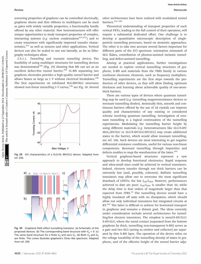
screening properties of graphene can be controlled electrically,graphene sheets and thin ribbons in multilayers can be usedas gates with widely variable properties, a functionality hardlyoffered by any other material. New heterostructures will offerunique opportunities to study transport properties of complex,interacting systems (e.g. exciton condensation431,432) and tocreate transistors with significantly improved transfer charac-teristics,433 as well as sensors and other applications. Verticaldevices can also be scaled to one nm laterally, as far as litho-graphy techniques allow.
2.9.1.1. Tunnelling and resonant tunnelling devices. Thefeasibility of using multilayer structures for tunnelling deviceswas demonstrated106 (Fig. 29) showing that BN can act as anexcellent defect-free tunnel barrier.106 1L-BN separating twographene electrodes provides a high-quality tunnel barrier andallows biases as large as 1 V without electrical breakdown.106
The first experiments on exfoliated SLG/BN/SLG structuresshowed non-linear tunnelling I–V curves,106 see Fig. 30. Several
other architectures have been realized with modulated tunnelbarriers.434–440
Theoretical understanding of transport properties of suchvertical FETs, leading to the full control of their operation, willrequire a substantial dedicated effort. One challenge is todevelop a quantitative microscopic description of single-particle tunnelling processes, based on atomistic approaches.The other is to take into account several factors important fordifferent parts of the I(V) spectrum: orientation mismatch ofSLG flakes, contribution of phonon-assisted inelastic tunnel-ling, and defect-assisted tunnelling.
Aiming at practical applications, further investigationsare needed to explore vertical tunnelling structures of gra-phene, h-BN and materials from the TMD family in variousnonlinear electronic elements, such as frequency multipliers.Tunnelling experiments are the first steps towards the pro-duction of other devices, as they will allow finding optimumthickness and learning about achievable quality of one-atom-thick barriers.
There are various types of devices where quantum tunnel-ling may be used (e.g. tunnelling magnetoresistance devices orresonant tunnelling diodes). Atomically thin, smooth and con-tinuous barriers offered by the use of 2d crystals can improvequality and characteristics of any existing or consideredscheme involving quantum tunnelling. Investigation of reso-nant tunnelling is a logical continuation of the tunnellingexperiments. Modulating the tunnelling barrier height byusing different materials (e.g. heterostructures like SLG/h-BN/MoS2/BN/SLG or SLG/h-BN/SLG/BN/SLG) may create additionalstates in the barrier, which would allow resonant tunnelling,see ref. 106. Such devices are most interesting to get negativedifferential resistance conditions, useful for various non-linearcomponents. Resonant tunnelling through impurities anddefects enables to map the wavefunction of the latter.441
Vertical graphene-based structures represent a newapproach to develop functional electronics. Rapid responseand ultra-small sizes could be achieved in vertical transistors.Indeed, electron transfer through nm thick barriers can beextremely fast (and, possibly, coherent). Ballistic tunnellingtransistors may allow one to overcome the most significantdrawback of GFETs: the low ION/IOFF. However, performancesachieved to date are poor: ION/IOFF is smaller than 20, whilethe delay time is four orders of magnitude larger than thatexpected from ITRS.12 The tunnelling devices would have ahighly insulated off state with no dissipation, which shouldallow not only individual transistors but integrated circuits atRT.442 The latter is difficult to achieve for horizontal transportin graphene and remains a distant goal. The ideas currentlyunder consideration include several architectures for tunnel-ling/hot electron transistors. The simplest is metal/h-BN/SLG/h-BN/SLG, where the metal contact (separated from the bottomgraphene by thick, tunnelling non-transparent h-BN) serves asa gate and two SLG (acting as emitter and collector) are separ-ated by thin h-BN layer. The operation of the device relies onthe voltage tunability of the tunnelling density of states in gra-phene, and of the effective height of the tunnel barrier adja-
Fig. 29 I(V) characteristics of a SLG/4L-BN/SLG device. Adapted fromref. 106.
Fig. 30 Graphene field-effect tunnelling transistor. (a) Schematic of theproposed devices. (b) The corresponding band structure with Vg = 0. (c)The same band structure for a finite Vg and zero Vb. (d) Both Vg and Vb
are finite. The cones illustrate graphene’s Dirac-like spectrum. Adaptedfrom ref. 106.
Review Nanoscale
4630 | Nanoscale, 2015, 7, 4598–4810 This journal is © The Royal Society of Chemistry 2015
Ope
n A
cces
s A
rtic
le. P
ublis
hed
on 2
2 Se
ptem
ber
2014
. Dow
nloa
ded
on 2
8/08
/201
5 13
:04:
01.
Thi
s ar
ticle
is li
cens
ed u
nder
a C
reat
ive
Com
mon
s A
ttrib
utio
n 3.
0 U
npor
ted
Lic
ence
.View Article Online

cent to the graphene electrode. It is interesting to experimentwith several different dielectrics in heterostructures, such asmetal/h-BN/SLG/MoS2/SLG. Higher quality heterostructures anddielectrics with smaller tunnelling barrier might bring ION/IOFFto 105–106, as required by modern electronics.
Another interesting idea is to attempt the development of ahot electron transistor, similar to those discussed in semicon-ductor electronics.443 Few-atom-thick transistors based on a 2dtunnelling barrier and graphene may allow much betterquality, and become more successful in applications. Thetransit time through such sandwiches is expected to be≪1 ps,443 whereas there are no limits for scaling down in thelateral dimension to true nm sizes. In a metal/h-BN/SLG/h-BN/SLG system, the thickness of the active part of the deviceswould be less than 10 atoms (∼3 nm) and should allow a bal-listic current controlled by the central graphene electrode. Theassembly of 2d crystals into superstructures may allow stacksof several transistors in series (metal/h-BN/SLG/h-BN/SLG)N in avertical integrated architecture.
2.9.1.2. Light emission and photovoltaics. Superstructures of2d crystals can be used to develop tunnelling LEDs and photo-voltaic cells. Here, we refer to superstructures composed oftwo conducting layers separated by a barrier with a modulatedprofile. Quantum wells are one example of heterostructuresmade by joining, directly at the atomic level, differentmaterials, usually in layers.444,445 A fundamental experimentalquantity is the “band offset ratio”, i.e. the ratio of the differ-ence in conduction band energies to the difference in valenceband energies.444,445 Heterostructures for which the differencein the band gap energies is largely dominated by the conduc-tion band offset are called “Type I” quantum wells.444,445
Those where e and h have their lowest energies in differentmaterials are called “Type II” quantum wells.444,445 Type-Iquantum wells (Fig. 31) can be used for injecting e/h, with sub-sequent recombination leading to light emission.
Using more complicated structures, both type-I and type-IIquantum wells of various configurations can be created. As theband-structure of 2d crystals depends on N, by changing thethickness of one component, one could tune the optical pro-perties. Using various thicknesses of different materials one
can target LEDs of different colours. As individual heterostruc-tures can be combined in one stack with individually con-tacted layers, LED at different wavelengths could be combinedin one structure.
Similarly, PV devices may be created by placing two metallic2d crystals (e.g. graphene) within tunnelling proximity of eachother. By applying a bias (or by exploiting the proximity effectof other metallic 2d crystals) electric field could be createdinside the barrier. Any e–h pair excited by light will be separ-ated and contribute to photocurrent.106 Similarly to the case ofLED, it should be possible to create heterostructures withvarious band gaps, sensitive to photons of different energies.Moreover, plasmonic nanostructures can improve the perform-ance of graphene photovoltaic devices.446
2.9.1.3. In situ characterization methods. Hybrid systemswill require advanced characterization, which should involveboth high spatial and/or point resolutions and coupling, pre-ferentially in situ. This will limit the contact with air, prevent-ing contamination. Two kinds of in situ coupling are worthconsidering: (i) coupling several characterization methods toinvestigate a single object, e.g. HRTEM + Raman spectroscopy+ electrical measurements, in order to accurately correlate thestructural features and the physical behaviour. (ii) Couplingone or several characterization methods (e.g., HRTEM imagingand electrical measurements) with one or several treatmentmethods (e.g., mechanical and/or thermal stresses) in order tocorrelate the variation of the behaviours with the structurechanges. Considering in situ TEM experiments, the abovecould be achieved by using sample holders equipped withvarious facilities (e.g., able to apply thermal or mechanicalstresses). However, there is the need to develop other sampleholders that will allow a larger panel of possible tests to beapplied to the samples under study. When the in situ couplingis technically difficult (e.g., coupling TEM and UV-Raman,which cannot be done through an optical fiber, or couplingTEM and high magnetic field inducer), a chip-based sampleholder technology will be highly preferred. Indeed, the latterwill allow the chip to be transferred from a characterizationsystem to another, each of them equipped with the appropriatesample holder bearing the same in situ treatment methods.This will allow various investigations on the same samplesunder the same conditions.
The chemical functionalization of graphene with reactivemolecules and the deposition of supramolecular assembliesrequire studying the self-organization process and themolecule/graphene interface in several conditions: At theliquid–solid interface, by wetting–dewetting processes, but alsoin connection with ultra-high vacuum (UHV) conditions. This isalready possible with UHV systems combining several sourcesof molecule deposition (sublimation, liquid-valve injection),with surfaces characterization techniques such as STM andX-ray and UV Photoelectron Spectroscopy. Several STM tech-niques are currently used: low temperature STS, Spin-polarizedSTM and Fourier-Transform Scanning Tunnelling Spectroscopy(STS), which can allow a local dispersion and surface Fermimeasurement. Synchrotron sources can be used for high resolu-
Fig. 31 SLG/h-BN/MoS2/h-BN/SLG structure: blue is the valence bandand pink is the conduction band. Adapted from ref. 106.
Nanoscale Review
This journal is © The Royal Society of Chemistry 2015 Nanoscale, 2015, 7, 4598–4810 | 4631
Ope
n A
cces
s A
rtic
le. P
ublis
hed
on 2
2 Se
ptem
ber
2014
. Dow
nloa
ded
on 2
8/08
/201
5 13
:04:
01.
Thi
s ar
ticle
is li
cens
ed u
nder
a C
reat
ive
Com
mon
s A
ttrib
utio
n 3.
0 U
npor
ted
Lic
ence
.View Article Online

tion ARPES, X-ray magnetic circular dichroism (XMCD) and alsospin-polarized low-energy electron microscopy, particularlyuseful for the ferromagnet/graphene interfaces.
2.9.1.4. Hybrid structures for active plasmonics. Combi-nations of 2d heterostructures with plasmonics would allowfor creation of active optical elements. 2d heterostructures areideally suited to be used with plasmonic structures, as theycan be positioned exactly at the maximum of electric field.Such elements are of great importance in different areas ofscience and technology: from displays, to frequency modu-lators. Despite great progress, active optics still relies heavilyon either liquid crystals,447 which guarantee deep modulationin inexpensive and small cells, but are quite slow,448 or non-linear optical crystals,449 which are fast,450 but bulky andexpensive.450 Thus, inexpensive, fast and small active opticalelements would be of considerable interest.
The target is the design and fabrication of a new generationof active plasmonic metamaterials with optical propertieselectrically controlled by 2d heterostructures. Plasmonic meta-materials of various configurations could be achieved by sand-wiching between SLG/h-BN heterostructures (see Fig. 32). Theconductivity of graphene can be changed by at least two ordersof magnitude with electrostatic doping.451 This could modulatethe optical properties of the under-lying plasmonic structure.The combination of 2d heterostructures with plasmonics couldresult in fast, cheap and small active optical elements.
2.10. Multiscale modelling of graphene-based structures andnew 2d crystals
The optimisation of active plasmonic materials will requiremultiscale modelling of their properties, taking into accountplasma modes and single-particle excitations, as well as theircoupling with flexural vibrations of individual layers. Furtherstudies should include modelling of heating of superstructuresand their cooling by lateral and vertical heat transfer.
Modelling of physical properties of new 2d crystals andhybrid devices constitutes an important research direction.A specialised effort is needed to provide timely interpretationof the characterisation of new 2d crystals, assessment/predic-tion of functional properties, and guidance of technologicaleffort in creation of hybrid structures (‘materials on demand’,see section 4.15). This will require the implementation of amultiscale modelling approach, in which the materials bandstructure and local microscopic parameters computed usingab initio simulations are incorporated in the mesoscale
description of electronic transport, thermal, mechanical, andoptical characteristics, which then enter into the finite-elementmodelling of operational devices or technological processes.
Many fundamental questions are open in the field of nano-electronics and new materials. Due to the complexity of both,these cannot be answered by conventional simplifiedapproaches. The research of novel functional materials ishighly interdisciplinary covering the domains of chemistry,material science, physics, and engineering with their methodsand scope of length scales. Advanced knowledge of such fieldshas necessarily to be combined. In addition, the complexityof quantum laws in nano-electronics complicates upscalingattempts to the point that, at the cross-road of new materialsand nanoelectronics (especially for beyond-CMOS appli-cations), only multiscale modelling approaches can progressknowledge sufficiently fast in the near future. The develop-ment of the necessary theoretical and computational methods,as well as improvement of the existing technologies, is there-fore needed and critical to the STR.
2.10.1. Ab initio computations. The theoretical explorationof structural and electronic properties of GRMs requires theextensive use of first-principles (or ab initio) computationalmethods. Especially, the modelling of material imperfections,such as structural defects (vacancies, Stone-Wales, grainboundaries), chemical modifications of the material surface(adatoms, molecular adsorbates), substrate or contact effectsbecomes crucial at the nanoscale, and such task can only beachieved using the proper level of electronic structure descrip-tion, including exchange and correlation effects with DFT, orextensions, such as the GW-correction452 and the time-depen-dent density functional theory (TDDFT),453 for graspingexcited states and optical spectra or low dimensional trans-port. The portfolio of such ab initio methods (mostly deve-loped by European consortia) is rich and diversified, offeringseveral levels of accuracy and scalability that will be appropri-ate depending on the system under study.
We provide a brief description of the general contours ofthe various levels of approximations to deal with electron cor-relations, together with a list of useful codes and a brief tech-nical description of their respective capabilities, in the contextof GRM studies. Most common ab initio methodologiesencompass the following approaches, all of which will requirefurther development: Hartree–Fock theory (H–F)454 and Post-Hartree–Fock (PH–F)455 quantum chemistry methods. Usually,H–F has insufficient accuracy for most purposes, but it pro-vides a good starting point for quantum chemistry configur-ation interaction methods, Møller–Plesset456 perturbationtheory and coupled-cluster457 methods. PH–F is highly accu-rate, but scales poorly with system size.458 Such codes gener-ally allow optimisation of geometry and calculation of a widerange of other properties.
DFT is the most “standard” ab initio approach, its mainlimitation being band gap underestimation.459 Either plane-wave or localised basis sets can be used, but this choice deter-mines the system size that can be simulated. The compu-tational cost of conventional DFT calculations scales with the
Fig. 32 Active plasmonic structure: Au dots sandwiched between SLG/h-BN layers.
Review Nanoscale
4632 | Nanoscale, 2015, 7, 4598–4810 This journal is © The Royal Society of Chemistry 2015
Ope
n A
cces
s A
rtic
le. P
ublis
hed
on 2
2 Se
ptem
ber
2014
. Dow
nloa
ded
on 2
8/08
/201
5 13
:04:
01.
Thi
s ar
ticle
is li
cens
ed u
nder
a C
reat
ive
Com
mon
s A
ttrib
utio
n 3.
0 U
npor
ted
Lic
ence
.View Article Online
cubic power of the number of atoms, O(N3), but linear-scaling[O(N)] DFT methods have been developed for insulators.460
DFT results can be mapped to tight-binding, to enable trans-port calculations (see, e.g., ref. 461, 462). Most DFT codesallow molecular and lattice dynamics calculations. The longstanding difficulty to deal with vdW forces463 was recently over-come,464 and several codes, such as AB-INIT or SIESTA(described below) now offer functionals that allow for an accu-rate description of vdW, a critical issue when dealing with elec-tronic properties of LMs (such as BN/graphene, graphene/graphene, etc.).
GW is the approximation to the self-energy of quasi-par-ticles in a many-body system, to obtain accurate excitationenergies.465 The methods generally scale as O(N4) but ref. 466reported a O(N3) implementation.467 GW can use the Bethe–Salpeter equation468 to describe excitonic effects,469,470 butscaling is O(N6).
TDDFT is the time-dependent formulation of the Kohn–Sham,471,472 equations, to calculate response functions.472
Poles of density–density response function correspond toexcited states. TDDFT is cheaper, but less accurate than GW,for determining excited-state energies.
Quantum Monte Carlo (QMC) is the most accurate totalenergy method for condensed matter physics.473 Scaling isO(N3), like standard DFT, but with a much greater prefactor.473
QMC is able to exploit massively parallel computers. Excitationenergies are accurate, but must be calculated one by one asdifferences of total energy. QMC molecular and latticedynamics will be available in the near future.
There is a manifold of codes suitable for the study of struc-tures and electronic features of GRMs. Among the most accu-rate DFT methods, usually based on plane-waves basis set, onecan consider AB-INIT, CASTEP, VASP or ADF described below.
AB INITio (ABINIT):474 A package that allows to calculate abroad number of molecular and periodic solids’ properties astotal energy, electronic structure and charge density, optimizedgeometries and dynamic simulations using calculated DFTforces and stresses, dynamical matrices, Born effectivecharges, dielectric tensors, excited states etc. The programs usecodes based on DFT, Density-Functional Perturbation Theory(DFPT), Many Body Perturbation Theory (GW approximationand Bethe–Salpeter equation) and TDDFT.
CAmbridge Serial Total Energy Package (CASTEP):475 a full-featured code based on a first-principles quantum mechanicaldescription of electrons and nuclei. It uses the robust methodsof a plane-wave basis set and pseudopotentials.
Vienna Ab initio Simulation Package (VASP):476 a plane-waveall-electron code using the projector-augmented wave methodto describe the electron–core interaction. The code uses fastiterative techniques for the diagonalization of the DFT Hamil-tonian and allows total-energy calculations and structuraloptimizations for systems with thousands of atoms andab initio molecular dynamics simulations for ensembles with afew hundred atoms extending over several tens of ps.
Amsterdam Density Functional (ADF):477,478 A suite basedon DFT that uses Slater-type orbitals479 as basic functions to
make electronic structure calculations, also able to performTDDFT. ADF can calculate various molecular properties likeIR, Raman, VCD (vibrational circular dichroism), UV and XAS(X-ray absorption spectroscopy) spectra, NMR and EPR (electricparamagnetic resonance) parameters, solvent and environ-mental effects.
Such methods are limited in terms of system size, andmainly restrict the exploration of material models few hun-dreds of atoms large. O(N) methods are implemented usinglocalized basis sets, gaining in upscalability but at the cost ofa reduced accuracy. Among the most useful: SIESTA, CON-QUEST, ONETEP, QUANTUM ESPRESSO, FLEUR, OCTOPUS.
Spanish Initiative for Electronic Simulations with Thou-sands of Atoms (SIESTA):480 a method and its computerprogram implementation, to perform efficient electronic struc-ture calculations and ab initio molecular dynamics simulationsof molecules and solids. SIESTA’s efficiency stems from theuse of strictly localized basis sets and from the implemen-tation of linear-scaling algorithms which can be applied tosuitable systems. Its accuracy and cost can be tuned in a widerange, from quick exploratory calculations to highly accuratesimulations matching the quality of other approaches, such asplane-wave and all-electron methods. VdW interaction hasbeen recently implemented.481
Concurrent O(N) QUantum Electronic Simulation Tech-nique (CONQUEST):482 A linear-scaling code based on DFT, toperform electronic structure calculations on very large systems,up to millions of atoms, with the possibility of choosingdifferent levels of accuracy.
Order-N Electronic Total Energy Package (ONETEP):483 alinear-scaling code for quantum-mechanical calculationsbased on non-orthogonal generalized Wannier func-tions,484,485 expressed in terms of periodic cardinal sine func-tions, in turn equivalent to a basis of plane-waves. ONETEPcombines the advantages of the plane-wave approach (control-lable accuracy and variational convergence of the total energywith respect to the size of the basis) with computational effortlinear with the size of the system.486
QUANTUM opEn Source Package for Research in ElectronicStructure, Simulation, and Optimization (QUANTUMESPRESSO487): an integrated suite of codes for electronic-struc-ture calculations and materials modelling, based on density-functional theory, plane waves, and pseudopotentials (norm-conserving, ultrasoft, and projector-augmented wave).QUANTUM ESPRESSO builds upon electronic-structure codesdeveloped and tested by the original authors of novel elec-tronic-structure algorithms, and applied over twenty years bysome of the leading materials modelling groups worldwide.
Jülich FLAPW code family (FLEUR):488 A code designed tocalculate properties of solids, based on the Full-potential Line-arized Augmented Plane-Wave (FLAPW) method.489
General Atomic and Molecular Electronic Structure System(GAMESS-UK):490 Gaussian-basis quantum chemistry code,with a variety of techniques for PH–F calculations.
OCTOPUS:491 A program aimed at the ab initio virtualexperimentation on, in principle, and ever-increasing range of
Nanoscale Review
This journal is © The Royal Society of Chemistry 2015 Nanoscale, 2015, 7, 4598–4810 | 4633
Ope
n A
cces
s A
rtic
le. P
ublis
hed
on 2
2 Se
ptem
ber
2014
. Dow
nloa
ded
on 2
8/08
/201
5 13
:04:
01.
Thi
s ar
ticle
is li
cens
ed u
nder
a C
reat
ive
Com
mon
s A
ttrib
utio
n 3.
0 U
npor
ted
Lic
ence
.View Article Online
system types. Electrons are described quantum-mechanicallywithin DFT, or TDDFT, when doing simulations in time.Nuclei are described classically as point particles. Electron–nucleus interaction is described within the pseudopotentialapproximation.
Other methods are more suitable for dealing with dynami-cal properties of materials, including the formation of stablestructures and or the highly accurate description of electron–electron correlations. Those include:
Cambridge quantum Monte Carlo computer programsystem (CASINO):492 A code based on QMC algorithms for con-tinuum electronic structures calculations using Slater–Jastrow493 pairing, and backflow wavefunctions or combi-nations of them. It is also possible to extend the range of wave-functions available.
Cornell-Holland Ab-initio Materials Package (CHAMP):494
A based on QMC algorithms designed to perform electronicstructure calculations on a wide variety of systems, such asatoms, clusters, solids, nanostructures and molecules.
Car–Parrinello Molecular Dynamics (CPMD):495 A plane-wave and pseudopotential DFT code designed for performingmolecular dynamics simulations, which can be used toperform TDDFT calculations.
CRYSTAL:496 A code designed to compute the electronicstructures of periodic systems based on H–F, DFT or hybridapproximations. Atom centred Gaussian functions form thebasis set that is linearly expanded into Bloch functions.
2.10.2. Mesoscale modelling. Despite the intensive soft-ware development, the computational cost of ab initiomethods still remains very expensive. This originates from thecomplexity of electrons represented by wave functions, hencepossessing an inner structure with widely variable propertiescompared to simple particles used in classical moleculardynamics. The requirement of self-consistency is only one con-sequence of the quantum nature, which slows down suchmethodology. Although many concepts exist to weaken thisimpact, there is a practical limitation to sizes of systems, atpresent ∼1–2 nm, treatable ab initio. This, however, is not thelength scale on which one discusses functional materials(at least one-two orders of magnitude above).
The characteristics and fundamental properties of interestfor functional materials are co-defined on a larger length scalebeyond the ab initio scope. This is because they are addition-ally influenced by other facts governing properties on suchlength scales, such as low concentration dopants, impuritiesor structural defects, or simply because the relevant structuresmay reach these dimensions themselves. Special attention hasto be paid to the interfaces or interaction of layers in multi-layer systems.
Multiscale modelling497 is capable of bridging lengthscales. The concept is based on the observation that not allinteractions must necessarily be treated within the first prin-ciples framework. This allows one to introduce a hierarchy ofinteractions, which might be founded either on very generalconsiderations or just adapted and valid for the presentlystudied properties. Based on this, a hierarchy of levels of treat-
ment may be introduced. The lowest (microscopic) level dealswith the smallest objects at the highest accuracy. It can beidentified with the full ab initio level. Multiscale modellingdefines first the models on each level and second the inter-faces for transferring relevant information to the respectiveupper (or even lower for feedback loop) level, where they arefurther processed. The advantage is that not all informationavailable on the computationally heavy lower level enters theupper-level modelling, but only relevant condensed infor-mation, which is precisely where multiscale modelling benefitsfrom. In addition, modelling of interactions on the uppermacroscopic level replaces respective couplings on the morerefined lower level. This allows one to reduce the work at thelower level by treating smaller parts (non-interacting subsys-tems) there. E.g., a finite range impact on electrostatics and onelectronic properties can be expected from impurities ordopants depending on the local surrounding of a host crystal.Additional long-range parts such as the Coulomb interactionmight be separable and can be treated on the upper level. Theinformation on local electronic properties can still be obtainedwith massively parallel ab initio methods using large super-cells. On the other hand, the evolution of a system as a whole,composed of millions of atoms, including a certain distri-bution of such dopants, is unpredictable by ab initio methodswhen the whole system is included at the same level.The problem is solved by combining local ab initio codes withspecialised solvers addressing mesoscale range of distances.Such combined codes include:
Learn on the Fly [LOTF]:498 hybrid quantum/classical mole-cular dynamics which combines quantum-mechanical embed-ding and classical force model optimization into a unifiedscheme free of the boundary region, and the transferabilityproblems which these techniques, taken separately, involve. Itis based on the idea of augmenting a unique, simple para-metrized force model by incorporating in it, at run time, thequantum-mechanical information necessary to ensure accu-rate trajectories. The scheme was tested on a number of Sisystems composed of up to approximately 200 000 atoms.499
SMEAGOL:500 DFT-based transport code which calculatestransport properties of atomic scale devices, using state of theart electronic structure calculation schemes.
Transport-Spanish Initiative for Electronic Simulations withThousands of Atoms [TranSiesta]:480 Extension of SIESTA withrecursive Green functions solver. The TranSiesta method is aprocedure to solve the electronic structure of an open systemformed by a finite structure sandwiched between two semi-infi-nite metallic leads. A finite bias can be applied between bothleads, to drive a finite current.
Tight-Binding Simulation [TB_sim]:501,502 tight-bindingcode which can be interfaced with SIESTA for more realisticdescriptions of structures and disorder.503 It is able tocompute the structural, electronic, optical and transport pro-perties of various nanostructures.
For a broader range of applications, including electronicand heat transport, optics, optoelectronics, thermomechanics,etc., alternative hybrid codes will need to be developed.
Review Nanoscale
4634 | Nanoscale, 2015, 7, 4598–4810 This journal is © The Royal Society of Chemistry 2015
Ope
n A
cces
s A
rtic
le. P
ublis
hed
on 2
2 Se
ptem
ber
2014
. Dow
nloa
ded
on 2
8/08
/201
5 13
:04:
01.
Thi
s ar
ticle
is li
cens
ed u
nder
a C
reat
ive
Com
mon
s A
ttrib
utio
n 3.
0 U
npor
ted
Lic
ence
.View Article Online
The treatment of disorder deserves particular attention.Indeed, to design a realistic scenario of the influence of dis-order on transport properties of materials and devices one hasto consider different length scales and modelling strategiessimultaneously. First, a microscopic picture of the atomicstructure is necessary to access electronic properties. This canonly be provided with state-of-the-art first principles simu-lations. These can be carried out using simple unit cells inclean systems. When considering crystal imperfections ordopants, larger supercells with few impurity atoms or defectsites are necessary.
The interface part is an essential ingredient of the model-ling. It defines which information is exchanged, i.e. which fea-tures of the ab initio-simulation are strong enough to beimportant on the macroscopic length scale. From these simu-lations one extracts electronic structure parameters which rep-resent at best the interactions at this level. For the efficiency ofthe multiscale approach it is very advantageous if the extractedparameters are generic. This should be considered whensetting up the modelling strategy to reduce or, at best, avoidfeedback effects. Quantum transport in chemically modifiedand disordered graphene-based materials can be successfullysimulated by means of novel types of O(N) algorithmsimplemented in the Landauer–Büttiker504 or Kubo–Green-wood505 formalisms (see, e.g., ref. 503, 506, 507). New direc-tions of work should include the effect of spin–orbit coupling,T effects or high bias regimes.
2.10.3. High performance computing. In the longer term,having a strong and realistic simulation capability will providea strategic tool to support product development in all fields ofapplications. In this perspective, supercomputing will be veryuseful for material characterization and device simulation at arealistic level. The use of High Performance Computing (HPC)is certainly necessary for making advances in frontier develop-ments in the fields of first-principles calculations and multi-scale methodologies. To make these new computationalschemes useful, supercomputers must be used intensively.However, one should note that the grand challenge is not justa question of computing faster and faster. E.g., for simulatingcomplex graphene-based devices (NEMS, sensors, transistors,or circuits), in addition to high performance computing, morephysical inspection of models and suitable use of first prin-ciples are needed.
GRM research will greatly benefit from a connection tosupercomputers facilities, especially for material simulation toserve as guidance applications. Improvements are required formultiscale modelling and reverse engineering, such asdecreasing the problem complexity, ideally to O(N). In DFTthis has already been achieved for insulators with the adventof O(N) codes.508 For other methods it is a far greater chal-lenge. Furthermore, it is essential to add functionality (theability to calculate a range of properties) to these codes, whilstretaining the favourable scaling.
Other improvements include increasing the ease of use(availability of documentation, support, examples, well-designed and clear input and output, ease of installation, etc.),
robustness (lack of bugs and numerical reliability), and“reverse engineering” tools to discover the technological prin-ciples of a device, object, or system through analysis of itsstructure, function, and operation.509
Broad cooperation between groups authoring the existingcodes is needed, for comparison between codes, for testingand optimisation purposes, development of better interfacesbetween codes, including better data standards, developmentsof methods that can exploit massively parallel computer facili-ties, development of “code libraries” and allowing problems tobe distributed among members of a community.
Developments made to first-principles algorithms andcodes will be equally useful in other areas of physics, chem-istry and materials science. First-principles codes and algori-thms aim to be general.
2.10.4. Further development of field-theory and kinetictheory methods. Analytical methods will play an equallyimportant role in the multiscale modelling of GRMs, providinga consistent scalability of materials parameters and a systema-tic description of GRMs in strongly non-equilibrium states.
The effects of e–e correlations, as well as the interplaybetween e–e interaction and disorder can be efficientlyaddressed using the renormalisation group approach.510 Thelatter enables one to follow non-trivial (non-linear) scaling ofmaterials parameters upon variation of the length scales atwhich the electron system is studied. It is based upon themicroscopic input (phenomenological or provided by DFTmodelling), permitting one to formulate a medium-energyeffective field theory describing the physical system, and it isfollowed by the analysis of the renormalisation flow of essen-tial constants in the theory, which may (or may not) be lengthscale dependent. The renormalisation group approach can beapplied to the studies of both quantum effects, like localis-ation in graphene, the interactions-driven phase transitionsinto states with spontaneously broken symmetry, and tostudies of classical problems related to the renormalisation offlexural deformations.
The development of efficient methods of kinetic theory isalso necessary, in order to treat graphene in strongly non-equi-librium conditions. As a thin material with a weak coupling tothe substrate/environment, graphene may easily overheat.511
Moreover, the energy relaxation of non-equilibrium carriers ingraphene (photoexcited or injected by tunnelling) requiresextensive modelling effort.512,513 Tackling graphene at highcurrent, reaching breakdown, is a more challenging theoreticalproblem, which requires the use of a combination of themicroscopic dynamics computation with the mesoscale kinetictheory.
2.10.5. Correlations in multiple graphene layers. e–e inter-action is relevant in BLG,514 where novel phases areexpected.515 A similar situation is expected in FLG with (trans-lational or rotational) stacking faults.
Apart from fundamental questions, a deeper understandingis relevant for potential applications, because of possible band-gaps induced by correlations that may compete with gaps in gra-phene nanostructures due to their spatial confinement.
Nanoscale Review
This journal is © The Royal Society of Chemistry 2015 Nanoscale, 2015, 7, 4598–4810 | 4635
Ope
n A
cces
s A
rtic
le. P
ublis
hed
on 2
2 Se
ptem
ber
2014
. Dow
nloa
ded
on 2
8/08
/201
5 13
:04:
01.
Thi
s ar
ticle
is li
cens
ed u
nder
a C
reat
ive
Com
mon
s A
ttrib
utio
n 3.
0 U
npor
ted
Lic
ence
.View Article Online
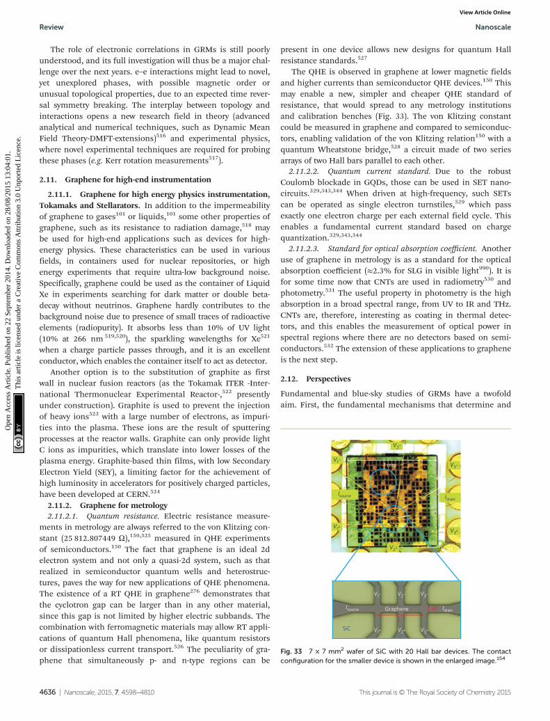
The role of electronic correlations in GRMs is still poorlyunderstood, and its full investigation will thus be a major chal-lenge over the next years. e–e interactions might lead to novel,yet unexplored phases, with possible magnetic order orunusual topological properties, due to an expected time rever-sal symmetry breaking. The interplay between topology andinteractions opens a new research field in theory (advancedanalytical and numerical techniques, such as Dynamic MeanField Theory-DMFT-extensions)516 and experimental physics,where novel experimental techniques are required for probingthese phases (e.g. Kerr rotation measurements517).
2.11. Graphene for high-end instrumentation
2.11.1. Graphene for high energy physics instrumentation,Tokamaks and Stellarators. In addition to the impermeabilityof graphene to gases101 or liquids,101 some other properties ofgraphene, such as its resistance to radiation damage,518 maybe used for high-end applications such as devices for high-energy physics. These characteristics can be used in variousfields, in containers used for nuclear repositories, or highenergy experiments that require ultra-low background noise.Specifically, graphene could be used as the container of LiquidXe in experiments searching for dark matter or double beta-decay without neutrinos. Graphene hardly contributes to thebackground noise due to presence of small traces of radioactiveelements (radiopurity). It absorbs less than 10% of UV light(10% at 266 nm 519,520), the sparkling wavelengths for Xe521
when a charge particle passes through, and it is an excellentconductor, which enables the container itself to act as detector.
Another option is to the substitution of graphite as firstwall in nuclear fusion reactors (as the Tokamak ITER -Inter-national Thermonuclear Experimental Reactor-,522 presentlyunder construction). Graphite is used to prevent the injectionof heavy ions523 with a large number of electrons, as impuri-ties into the plasma. These ions are the result of sputteringprocesses at the reactor walls. Graphite can only provide lightC ions as impurities, which translate into lower losses of theplasma energy. Graphite-based thin films, with low SecondaryElectron Yield (SEY), a limiting factor for the achievement ofhigh luminosity in accelerators for positively charged particles,have been developed at CERN.524
2.11.2. Graphene for metrology2.11.2.1. Quantum resistance. Electric resistance measure-
ments in metrology are always referred to the von Klitzing con-stant (25 812.807449 Ω),150,525 measured in QHE experimentsof semiconductors.150 The fact that graphene is an ideal 2delectron system and not only a quasi-2d system, such as thatrealized in semiconductor quantum wells and heterostruc-tures, paves the way for new applications of QHE phenomena.The existence of a RT QHE in graphene276 demonstrates thatthe cyclotron gap can be larger than in any other material,since this gap is not limited by higher electric subbands. Thecombination with ferromagnetic materials may allow RT appli-cations of quantum Hall phenomena, like quantum resistorsor dissipationless current transport.526 The peculiarity of gra-phene that simultaneously p- and n-type regions can be
present in one device allows new designs for quantum Hallresistance standards.527
The QHE is observed in graphene at lower magnetic fieldsand higher currents than semiconductor QHE devices.150 Thismay enable a new, simpler and cheaper QHE standard ofresistance, that would spread to any metrology institutionsand calibration benches (Fig. 33). The von Klitzing constantcould be measured in graphene and compared to semiconduc-tors, enabling validation of the von Klitzing relation150 with aquantum Wheatstone bridge,528 a circuit made of two seriesarrays of two Hall bars parallel to each other.
2.11.2.2. Quantum current standard. Due to the robustCoulomb blockade in GQDs, those can be used in SET nano-circuits.329,343,344 When driven at high-frequency, such SETscan be operated as single electron turnstiles,529 which passexactly one electron charge per each external field cycle. Thisenables a fundamental current standard based on chargequantization.329,343,344
2.11.2.3. Standard for optical absorption coefficient. Anotheruse of graphene in metrology is as a standard for the opticalabsorption coefficient (≈2.3% for SLG in visible light990). It isfor some time now that CNTs are used in radiometry530 andphotometry.531 The useful property in photometry is the highabsorption in a broad spectral range, from UV to IR and THz.CNTs are, therefore, interesting as coating in thermal detec-tors, and this enables the measurement of optical power inspectral regions where there are no detectors based on semi-conductors.532 The extension of these applications to grapheneis the next step.
2.12. Perspectives
Fundamental and blue-sky studies of GRMs have a twofoldaim. First, the fundamental mechanisms that determine and
Fig. 33 7 × 7 mm2 wafer of SiC with 20 Hall bar devices. The contactconfiguration for the smaller device is shown in the enlarged image.154
Review Nanoscale
4636 | Nanoscale, 2015, 7, 4598–4810 This journal is © The Royal Society of Chemistry 2015
Ope
n A
cces
s A
rtic
le. P
ublis
hed
on 2
2 Se
ptem
ber
2014
. Dow
nloa
ded
on 2
8/08
/201
5 13
:04:
01.
Thi
s ar
ticle
is li
cens
ed u
nder
a C
reat
ive
Com
mon
s A
ttrib
utio
n 3.
0 U
npor
ted
Lic
ence
.View Article Online
may limit their potential in already foreseen electronic andoptoelectronics applications should be uncovered. Second, thenext generation of GRM-based nanostructures for the develop-ment of electronic devices beyond CMOS needs to be devel-oped. Research is needed to gain in-depth understanding ofmicroscopic properties of defects in crystal graphene, GBs inpolycrystalline graphene, or the influence of environment(such as various substrates), all factors jeopardizing the per-formances of mass-produced devices. The engineering of elec-trical circuits incorporating GNRs and GQDs will be essentialto exploit the new functionalities of graphene in high-endinstrumentation and metrology.154 The study of 2d crystalsbeyond graphene5,38 is also key to enhance graphene’s pro-perties by combining this material with monolayers of 2d crys-tals in superstructures, which will allow broadening of therange of functional applications of graphene and hybrid super-structures in post-CMOS electronics.
The objectives foreseen in the next few years are:• To establish the fundamental limits for functional gra-
phene nanostructures in electronics beyond CMOS.This can be achieved via microscopic characterisation of
single- and poly-crystalline graphene and graphene-basednanostructures, studies of kinetic processes, influence ofdefects, disorder, and influence of substrate/environment onelectronic properties.
• To explore the use of LMs in electronics.This will include microscopic characterisation of electronic
properties of 2d crystals, studies of their transport and verticaltunnelling properties, and multi-scale modelling of graphene-based and hybrid structures.
The long-term objectives are:• To exploit graphene for both classical and quantum infor-
mation processing in the post-CMOS era.For classical information processing, the development of
vertical transistors and atomic scale metal–semiconductorfield effect transistor (MESFETs) where graphene is used asactive component, as interconnect, or transparent gate is a keyobjective. For quantum information processing, the exploita-tion of the long-lived spin coherence of electrons in grapheneis needed to develop monolayer and bilayer QD qubits, read-outs, and their scalable circuits.
• To build graphene-based metrological applications andhigh-end electronic instrumentation.
For metrology and standardisation, it is fundamental todevelop transferable table-top quantum resistance standardsbased on the quantum Hall effect, and stable quantisedcurrent sources. High-end instrumentations will includehighly sensitive bolometers, ultra-sensitive Hall probes, andnew types of scanning probes.
• To produce new inorganic 2d crystals, systematically inves-tigate their physical properties, and evaluate the potential foroptoelectronic applications.
Using the experience developed with graphene, the long-term vision is to explore a broad range of LMs beyond gra-phene. The issues that need to be addressed will includematerial stability, compatibility with nanofabrication pro-
cesses, and the entire range of structural, optical and electricalcharacterisation.
• To study electronic, optical, and thermo-mechanical pro-perties of hybrids combining graphene with various 2dcrystals.
The microscopic charge transfer and transport in multilayerhybrid structures, optical processes and hot carrier dynamics,electron spin memory and relaxation need to be studied.Understanding these processes will enable the development ofdevices such as transistors and switches, LEDs, PV cells andphoto-detectors.
The timeline is shown in Fig. 34. Timescales: 2–3 years:understanding fundamental kinetic processes and influenceof defects. 4–7 years: Understanding of electronic, optical, andthermo-mechanical properties of hybrid structure combininggraphene with various 2d crystals that have electronic band-gaps and establishing their fundamental limitation. 7–10years: Integration of vertical hybrid devices and developmentof graphene-based metrological systems and high-end elec-tronic instrumentation.
3. Health and environment
Nanosafety, defined as all the safety issues associated withnanotechnology, is crucially required to translate any futuredevelopment of new nanotechnologies into action, from indus-trial applications to health care approaches.533–536 GRMs arenot devoid of possible risks on health or environment,and cannot be excluded from these two domains of investi-gation. It is of fundamental importance to explore the level oftoxicity and to establish, if required, constrains for safetyof use.537–542
The GRM small size and unique physico-chemical pro-perties may pose potential health and environment risks.Determining and resolving safety and toxicity issues will notonly be beneficial for integration into devices, but also in lightof possible biomedical applications, such as direct nano-inter-facing devices with cells and tissues.
Initial studies have assessed the in vitro and in vivo toxicityof graphene and graphene oxide (GO), while for other 2d crys-tals very little has been done to date. Some of these studiesshowed that there are no particular risks for using GRMs, con-versely others have evidenced that some forms might becomea health hazard.537–542 When manipulating a nanomaterial,inhalation is one of the possible ways of contact. Some GRMshave aerodynamic size that may lead to inhalation and depo-sition into the respiratory apparatus with implications on theformation of granulomas and lung fibrosis.543 On the otherhand, the possible biological effects and responses can differdepending on the chemico-physical properties (i.e. N, lateralsize, stiffness, hydrophobicity, and surface functionalization),the administered dose and the purity. Limited data542 areavailable on the difference in biological behaviour betweenlarge (few micron lateral size) and small (few hundred nano-
Nanoscale Review
This journal is © The Royal Society of Chemistry 2015 Nanoscale, 2015, 7, 4598–4810 | 4637
Ope
n A
cces
s A
rtic
le. P
ublis
hed
on 2
2 Se
ptem
ber
2014
. Dow
nloa
ded
on 2
8/08
/201
5 13
:04:
01.
Thi
s ar
ticle
is li
cens
ed u
nder
a C
reat
ive
Com
mon
s A
ttrib
utio
n 3.
0 U
npor
ted
Lic
ence
.View Article Online
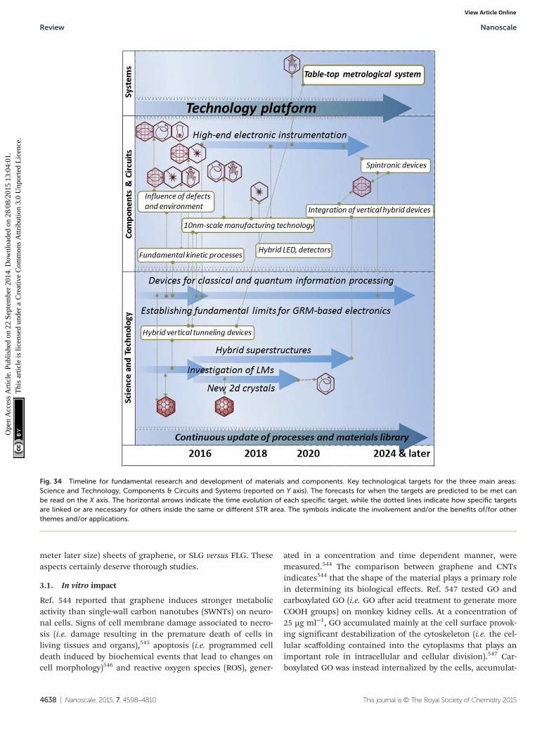
meter later size) sheets of graphene, or SLG versus FLG. Theseaspects certainly deserve thorough studies.
3.1. In vitro impact
Ref. 544 reported that graphene induces stronger metabolicactivity than single-wall carbon nanotubes (SWNTs) on neuro-nal cells. Signs of cell membrane damage associated to necro-sis (i.e. damage resulting in the premature death of cells inliving tissues and organs),545 apoptosis (i.e. programmed celldeath induced by biochemical events that lead to changes oncell morphology)546 and reactive oxygen species (ROS), gener-
ated in a concentration and time dependent manner, weremeasured.544 The comparison between graphene and CNTsindicates544 that the shape of the material plays a primary rolein determining its biological effects. Ref. 547 tested GO andcarboxylated GO (i.e. GO after acid treatment to generate moreCOOH groups) on monkey kidney cells. At a concentration of25 µg ml−1, GO accumulated mainly at the cell surface provok-ing significant destabilization of the cytoskeleton (i.e. the cel-lular scaffolding contained into the cytoplasms that plays animportant role in intracellular and cellular division).547 Car-boxylated GO was instead internalized by the cells, accumulat-
Fig. 34 Timeline for fundamental research and development of materials and components. Key technological targets for the three main areas:Science and Technology, Components & Circuits and Systems (reported on Y axis). The forecasts for when the targets are predicted to be met canbe read on the X axis. The horizontal arrows indicate the time evolution of each specific target, while the dotted lines indicate how specific targetsare linked or are necessary for others inside the same or different STR area. The symbols indicate the involvement and/or the benefits of/for otherthemes and/or applications.
Review Nanoscale
4638 | Nanoscale, 2015, 7, 4598–4810 This journal is © The Royal Society of Chemistry 2015
Ope
n A
cces
s A
rtic
le. P
ublis
hed
on 2
2 Se
ptem
ber
2014
. Dow
nloa
ded
on 2
8/08
/201
5 13
:04:
01.
Thi
s ar
ticle
is li
cens
ed u
nder
a C
reat
ive
Com
mon
s A
ttrib
utio
n 3.
0 U
npor
ted
Lic
ence
.View Article Online

ing in the perinuclear region, without affecting the mor-phology of F-actin filaments (a protein, found in all eukaryoticcells, that forms microfilaments).547 GO affected the cell viabi-lity at 50 µg ml−1, while carboxylated hydrophilic GO was nottoxic up to 300 µg ml−1.547 The lack of a careful definition ofthe materials (e.g. calling pristine graphene what is insteadGO) creates confusion when cytotoxic profiles of differentnanocarbons are to be compared. Other studies on differentcell lines reported dose and time dependent GO effects on cellviability only at concentration above 80 µg ml−1,548–550 andchanges in cell morphology only after long time culturing.551
Ref. 552, 553 reported that GO induced time and concen-tration dependent cell mortality, as documented by the earlyand late presence of apoptotic cells.
To expand the analysis of the cellular responses induced byGO, sheets of different lateral sizes (i.e. 350 nm and 2 µm)were tested.554 Two phagocytic cell lines (i.e. with the capacityof engulfing solid particles) were able to internalize nano-sizedand micro-sized GO.554 Little differences on cell viability wereobserved up to 20 µg ml−1.554 However, the presence of manga-nese as contaminant, due to inaccurate purification pro-cedures during the oxidative process to prepare GO, induced aGO-independent high cell death.554 This shows how accuratepurification steps are relevant in avoiding false positives, thatmight be erroneously associated to an undesired effect of thenanomaterial itself. In addition, in the phagocytes tested, theuptake and sub-cellular localizations of the two GOs of 350 nmand of 2 µm, were different. The larger GO sheets induced alsoa stronger inflammatory response. The different behaviours ofthe two types of GOs can be exploited on different biomedicalcontexts. The high inflammatory responses of micro-sized GO(2 µm) can be used to promote adjuvant effects (that modifythe effect of other agents) in vaccine systems to strengthenweak immune responses. The low inflammatory profilesassociated to nano-sized GO (350 nm) can be useful for appli-cations in cancer therapy, where improved biocompatibility isnecessary. The study of the effects on macrophages (i.e. cells ofthe immune system capable to phagocytose, i.e. engulf anddigest, cellular debris and pathogens555) was then extendedto graphene dispersed in 1% surfactant (Pluronic F108).555 Inthis experiment, murine macrophages underwent apoptosisthrough decrease of mitochondrial potential and ROSincrease. To identify the mechanisms that trigger macrophageapoptosis is important as it provides information to developstrategies to control cell death induced by graphene. BesidesPluronic, other polymers were shown to improve the biocom-patibility of GO and RGO.556
In developing graphene and GO as therapeutic deliverysystems of molecules via systemic administration, it is impor-tant to evaluate their interaction with blood cells.557,558 Whentested, both graphene and GO showed little haemolysis (i.e.rupturing of red blood cells) (max. dose of 75 µg ml−1).557 Hae-molytic activity was completely suppressed by coating GO withthe polysaccharide chitosan.558 In addition, platelets exhibitednormal morphology and were not activated or aggregated. Thecoagulation pathways were also not influenced, predictive of
low risk of thrombosis once intravenously administered.However, two additional studies reported opposite results andevidenced potential thrombotoxicity risks of GO.559,560 Thesecytotoxic effects were modulated by reducing the carboxylicfunctions of GO with thermal annealing,559 or by transformingthem into ammonium groups.560 This second transformationled to a new modified GO with no effect on platelet stimu-lation, nor lysis of erythrocytes (i.e. red blood cells) andabsence of thromboembolysis (i.e. embolisms due to bloodcoagulation). What is unclear is the efficiency of the transform-ation of the carboxylic groups into amines as GO contains alsoother types of oxygenated functions that should not undergothe chemical transformation following the Curtius rearrange-ment (i.e. transformation of the carboxylic groups intoamines),561,562 applied to GO. When GO was treated withhydrazine to generate RGO, it was highly cytotoxic, loweringcell viability.549
Alternatively to the reduction with hydrazine, other chemi-cal strategies were used to modify GO. Covalent modificationwith polyethylene glycol (PEG) chains (PEGylation) had theeffect to modulate the cytotoxic effect on a series of cell lines,without affecting cell viability up to 100 µg ml−1.563,564
Cytotoxicity of GO was also reduced by functionalization withdextran, a biocompatible polymer widely used for surfacecoating of biomaterials.565
Ref. 566 carried out a biocompatibility assessment of bothCVD and LPE graphene using cultured human lung epithelialcell line A549. No detectable changes in the cellular mor-phology of A549 cells growing on graphene thin films or cellsexposed to graphene flakes (0.1 to 5 μg mL−1) for 4 to 72 h wasobserved.566 In contrast, the same work outlined how carbonblack is significantly more toxic than graphene.566
This set of results represents a significant first step towardsthe experimental assessment of the in vitro toxicity of grapheneand GO. However, to avoid the generalization often found forother carbon-based nanomaterials, such as CNTs,539 it isnecessary to take into consideration the great variability of thematerials tested. It is essential to compare graphene and GOas well as other GRMs and correlate their impact on cells totheir physico-chemical characteristics and, in case, to thechemical changes introduced.
3.2. Cytotoxicity effects on graphene-coated surfaces
The evaluation of the cytotoxic effects of graphene and GO hasalso important implications on their use as support for tissueregeneration, cell growth, cell differentiation, and for thedevelopment of implantable devices (Fig. 35).567,568
Preliminary studies already explored graphene ability tointerface neurons.569 Mouse hippocampal cells were culturedon a graphene substrate to test if the neural functions wereaffected during their development and maturation in vitro.569
The results revealed high biocompatibility of such growthsurface, with low toxicity in the absence of morphologicalchanges.569 The potential use of graphene in neuronal inter-facing thus represents a promising approach in future develop-ments of neural prosthesis. Similarly, different surfaces
Nanoscale Review
This journal is © The Royal Society of Chemistry 2015 Nanoscale, 2015, 7, 4598–4810 | 4639
Ope
n A
cces
s A
rtic
le. P
ublis
hed
on 2
2 Se
ptem
ber
2014
. Dow
nloa
ded
on 2
8/08
/201
5 13
:04:
01.
Thi
s ar
ticle
is li
cens
ed u
nder
a C
reat
ive
Com
mon
s A
ttrib
utio
n 3.
0 U
npor
ted
Lic
ence
.View Article Online

covered by graphene were also able to induce progenitor celldifferentiation.570 In particular, graphene allowed to controland to accelerate the proliferation of human mesenchymalstem cells (i.e. multipotent connective tissue cells that candifferentiate into a variety of cell types). Cell viability was main-tained and no change in cell morphology was observed duringthe differentiation process, which was enhanced in the case ofthe cells in direct contact with graphene in comparison toother types of surfaces, like glass or Si wafers.570 This studyrepresents an interesting example where bone regenerationcan be achieved in the absence of growth factors, usuallyrequired to boost this process.570 It also hints at the safety ofgraphene when it remains intact after cell growth. This opensthe possibility of actively integrating it into devices design tofavour tissue regeneration or repair.
3.3. In vivo impact, biodistribution and pharmacokinetics
Additional studies investigating toxicity in vivo,559,560 comple-mented those in vitro,559,560 directed to assess the impact ofGO at the cellular level. Intravenous administration of GO inmice elicited blood platelets aggregation and extensive pul-monary thromboembolism.559,560 This behaviour was associ-ated to the presence of charged functional groups on GO, asthe aggregation properties were significantly lowered, when itwas chemically transformed into RGO.560 In vivo toxicity of GOwas evaluated in mice and rats following intravenous adminis-tration after labelling with a radiotracer.571 Significant patho-logical changes, including inflammatory cell infiltration,pulmonary aedema and formation of granulomas were foundat a dose of 10 mg kg−1.571 These results were confirmed byanother study in which GO, injected in mice, induced granulo-mas in lungs, spleen and liver.553
Pulmonary toxicity is a major concern in the industrial pro-duction of nanomaterials, as their volatile nature favours inha-lation and might directly cause acute damages and long termdiseases. It was reported572 that GO provokes severe and per-sistent injury in mice lungs following direct injection into theorgans.572 However, this form of toxicity was reduced whengraphene was dispersed in a surfactant (i.e. Pluronic).572 Inanother study,543 the exposure risks of the respiratory system
were also suggested for graphene nanoplatelets (25 µm lateralsize) dispersed in bovine serum albumin.543 Following theinhalation, the nanoplatelets were found to deposit beyond therespiratory tract. Acute inflammatory responses in mice,inflammation and frustrated macrophage phagocytosis (occur-ring when a phagocyte is unable to engulf its target because itis physically too large) were reported.543 The inflammogenicity(i.e. the ability to sustain long-term inflammatory activity) wasattributed to the inhalable aerodynamic diameter,543 an indexthat determines the respirability of a particle and the site ofdeposition. The differences in these two studies, both testinggraphene dispersed in surfactants, are likely due to thedifferent morphology of the materials used, in terms ofN, surface area, dispersion procedures, and/or the presence ofcontaminants. These parameters can favour variable toxicityprofiles. The ability to manipulate graphene’s toxicity profile issupported by the evidence that extensively purified GO doesnot affect polymorphonuclear leukocytes (i.e. white blood cellscontaining segmented lobular nucleus) even after 7 days ofperitoneal administration.573 No giant cells, inflammatoryresponse and granuloma were observed in comparison to pris-tine multi wall nanotubes (MWNTs).574 The modulation of tox-icity in vivo can also be achieved through functionalization.It was reported that GO PEGylation can reduce toxic effects inmice.564
The study of the biodistribution, accumulation and elimin-ation of graphene and GO in vivo is another key step to predictand avoid any user’s risk.574,575 Biodistribution studies haveshown that GO accumulates predominantly in the lungs,571,574
while low uptake was observed in the reticuloendothelialsystem – RES (i.e. the part of the immune system that consistsof the phagocytic cells located in reticular connective tissue.The cells are primarily monocytes and macrophages, and theyaccumulate in lymph nodes and the spleen. The Kupffer cellsof the liver are also part of the RES).571,574 GO exhibited longcirculation time (several hours) in comparison to other carbonforms like CNTs.571,574 While no pathological modifications inthe organs were reported after 14 days following the injectionof 1 mg per kg of body weight,571,574 significant changes wereobserved in the lungs at a dose of 10 mg kg−1. PEGylated GOinstead accumulated mainly in the tumour of tumour-bearinganimals, with lower uptake by RES, without significant toxiceffects.574 The same type of material was intravenouslyinjected, after being radiolabelled, to better elucidate theorgan biodistribution and the excretion routes.575 Followingan initial accumulation in the RES, a gradual elimination wasobserved between 3 and 15 days.575 After three months, theGO sheets were completely eliminated without toxic effects.575
No signs of abnormality were observed in kidney, liver, spleen,heart and lung.575 This GO was further studied to evaluatemore thoroughly the pharmacokinetics and the long-term bio-distribution. These parameters were analyzed by radiolabellingthe GO with 125I.575 After intravenous administration, the GOsheets were found to accumulate into the RES includingspleen and liver.575 They were gradually cleared by both renaland faecal elimination.575 A dose of 20 mg kg−1 did not
Fig. 35 Schematic representation of cells (coloured in purple and withtheir nucleus in blue) in contact with a surface of graphene (representedas black balls and sticks).
Review Nanoscale
4640 | Nanoscale, 2015, 7, 4598–4810 This journal is © The Royal Society of Chemistry 2015
Ope
n A
cces
s A
rtic
le. P
ublis
hed
on 2
2 Se
ptem
ber
2014
. Dow
nloa
ded
on 2
8/08
/201
5 13
:04:
01.
Thi
s ar
ticle
is li
cens
ed u
nder
a C
reat
ive
Com
mon
s A
ttrib
utio
n 3.
0 U
npor
ted
Lic
ence
.View Article Online
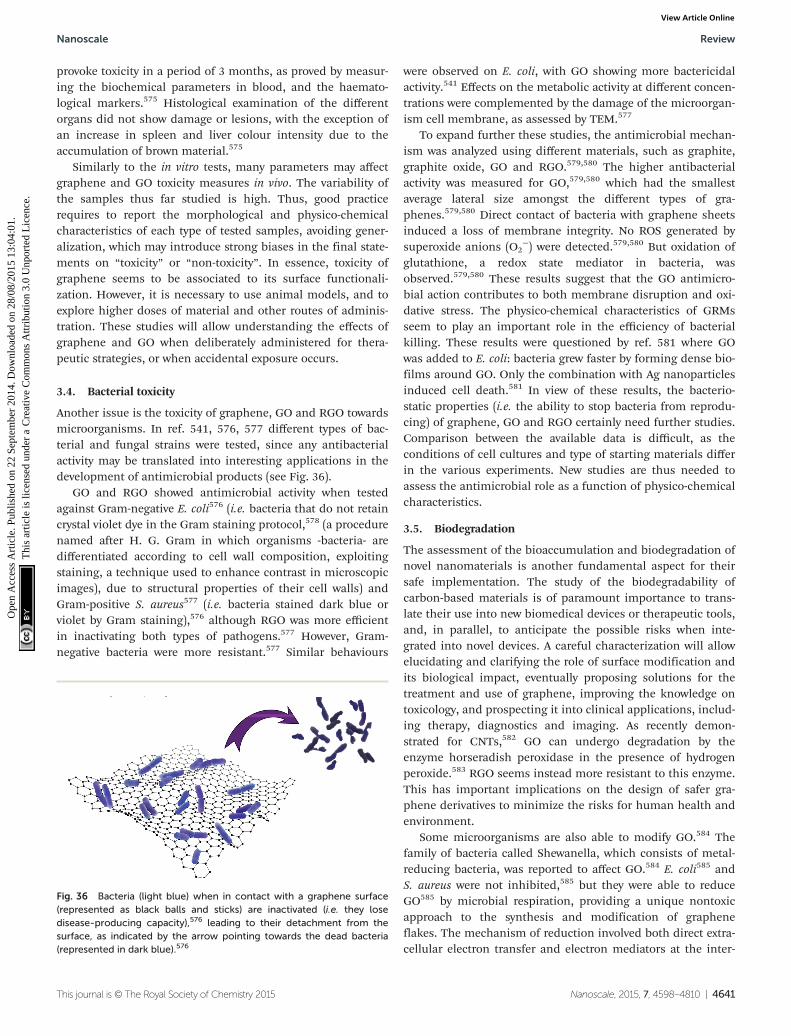
provoke toxicity in a period of 3 months, as proved by measur-ing the biochemical parameters in blood, and the haemato-logical markers.575 Histological examination of the differentorgans did not show damage or lesions, with the exception ofan increase in spleen and liver colour intensity due to theaccumulation of brown material.575
Similarly to the in vitro tests, many parameters may affectgraphene and GO toxicity measures in vivo. The variability ofthe samples thus far studied is high. Thus, good practicerequires to report the morphological and physico-chemicalcharacteristics of each type of tested samples, avoiding gener-alization, which may introduce strong biases in the final state-ments on “toxicity” or “non-toxicity”. In essence, toxicity ofgraphene seems to be associated to its surface functionali-zation. However, it is necessary to use animal models, and toexplore higher doses of material and other routes of adminis-tration. These studies will allow understanding the effects ofgraphene and GO when deliberately administered for thera-peutic strategies, or when accidental exposure occurs.
3.4. Bacterial toxicity
Another issue is the toxicity of graphene, GO and RGO towardsmicroorganisms. In ref. 541, 576, 577 different types of bac-terial and fungal strains were tested, since any antibacterialactivity may be translated into interesting applications in thedevelopment of antimicrobial products (see Fig. 36).
GO and RGO showed antimicrobial activity when testedagainst Gram-negative E. coli576 (i.e. bacteria that do not retaincrystal violet dye in the Gram staining protocol,578 (a procedurenamed after H. G. Gram in which organisms -bacteria- aredifferentiated according to cell wall composition, exploitingstaining, a technique used to enhance contrast in microscopicimages), due to structural properties of their cell walls) andGram-positive S. aureus577 (i.e. bacteria stained dark blue orviolet by Gram staining),576 although RGO was more efficientin inactivating both types of pathogens.577 However, Gram-negative bacteria were more resistant.577 Similar behaviours
were observed on E. coli, with GO showing more bactericidalactivity.541 Effects on the metabolic activity at different concen-trations were complemented by the damage of the microorgan-ism cell membrane, as assessed by TEM.577
To expand further these studies, the antimicrobial mechan-ism was analyzed using different materials, such as graphite,graphite oxide, GO and RGO.579,580 The higher antibacterialactivity was measured for GO,579,580 which had the smallestaverage lateral size amongst the different types of gra-phenes.579,580 Direct contact of bacteria with graphene sheetsinduced a loss of membrane integrity. No ROS generated bysuperoxide anions (O2
−) were detected.579,580 But oxidation ofglutathione, a redox state mediator in bacteria, wasobserved.579,580 These results suggest that the GO antimicro-bial action contributes to both membrane disruption and oxi-dative stress. The physico-chemical characteristics of GRMsseem to play an important role in the efficiency of bacterialkilling. These results were questioned by ref. 581 where GOwas added to E. coli: bacteria grew faster by forming dense bio-films around GO. Only the combination with Ag nanoparticlesinduced cell death.581 In view of these results, the bacterio-static properties (i.e. the ability to stop bacteria from reprodu-cing) of graphene, GO and RGO certainly need further studies.Comparison between the available data is difficult, as theconditions of cell cultures and type of starting materials differin the various experiments. New studies are thus needed toassess the antimicrobial role as a function of physico-chemicalcharacteristics.
3.5. Biodegradation
The assessment of the bioaccumulation and biodegradation ofnovel nanomaterials is another fundamental aspect for theirsafe implementation. The study of the biodegradability ofcarbon-based materials is of paramount importance to trans-late their use into new biomedical devices or therapeutic tools,and, in parallel, to anticipate the possible risks when inte-grated into novel devices. A careful characterization will allowelucidating and clarifying the role of surface modification andits biological impact, eventually proposing solutions for thetreatment and use of graphene, improving the knowledge ontoxicology, and prospecting it into clinical applications, includ-ing therapy, diagnostics and imaging. As recently demon-strated for CNTs,582 GO can undergo degradation by theenzyme horseradish peroxidase in the presence of hydrogenperoxide.583 RGO seems instead more resistant to this enzyme.This has important implications on the design of safer gra-phene derivatives to minimize the risks for human health andenvironment.
Some microorganisms are also able to modify GO.584 Thefamily of bacteria called Shewanella, which consists of metal-reducing bacteria, was reported to affect GO.584 E. coli585 andS. aureus were not inhibited,585 but they were able to reduceGO585 by microbial respiration, providing a unique nontoxicapproach to the synthesis and modification of grapheneflakes. The mechanism of reduction involved both direct extra-cellular electron transfer and electron mediators at the inter-
Fig. 36 Bacteria (light blue) when in contact with a graphene surface(represented as black balls and sticks) are inactivated (i.e. they losedisease-producing capacity),576 leading to their detachment from thesurface, as indicated by the arrow pointing towards the dead bacteria(represented in dark blue).576
Nanoscale Review
This journal is © The Royal Society of Chemistry 2015 Nanoscale, 2015, 7, 4598–4810 | 4641
Ope
n A
cces
s A
rtic
le. P
ublis
hed
on 2
2 Se
ptem
ber
2014
. Dow
nloa
ded
on 2
8/08
/201
5 13
:04:
01.
Thi
s ar
ticle
is li
cens
ed u
nder
a C
reat
ive
Com
mon
s A
ttrib
utio
n 3.
0 U
npor
ted
Lic
ence
.View Article Online
face between cells and flakes. This work should be extended toother microorganisms, not only to modify, but eventually todegrade graphene.
3.6. Environmental impact
To our knowledge, to date there are almost no studies thatfocus on the ecotoxicity and environmental impact of gra-phene, GO and RGO.541 The majority of data in literature con-cerns fullerenes.586 These studies highlight the effect offullerene ingestion and its associated toxicity in several modelorganisms: fresh water crustaceans,586 marine copepods586
and fish.586 Several data are also currently available on the eco-toxicological effects of CNTs in various organisms.587 Moststudies on CNT ecotoxicity were conducted on representativespecies of the aquatic environment,588–590 and, to a lesserextent, on terrestrial organisms.591,592 Based on the experienceacquired with these carbons, it is mandatory to explore theimpact of GRMs on the environment. It is necessary to developand broaden our knowledge in this area in order to betterunderstand the potential effects on the environment in theshort or long term, and to adopt adequate disposal pro-cedures. With the development of graphene technology, it isessential to assess exposure in real-life conditions and to fullyunderstand the graphene life-cycle, otherwise any assessmentof occupational or environmental effects will remainuncertain.
Thus far, only few studies addressed the influence of gra-phene on terrestrial plants.593 Phytotoxicity (i.e. toxic effectson plant growth) at concentrations of GO between 500 and2000 µg ml−1 was studied in cabbage, tomato, red spinach andlettuce.593 Root and shoot growth, biomass, shape, cell deathand generation of ROS were evaluated.593 After 20 days ofexposure, the plants treated with GO displayed a reducednumber of leaves.593 The growth and biomass were inhibitedwith visible symptoms of necrosis and increased ROS.593 Theonly exception was lettuce seedlings.593 These effects weredose and time dependent.593 Particular attention needs to bedevoted to possible adverse effects of graphene on plant cells.Similarly, GO sheets were tested on the germination of riceseeds in comparison to other carbon nanomaterials such asCNTs and fullerenes.594 While, e.g., CNTs were found to favouran increase in water content during germination,594 GOretarded the development and reduced the water content.594 Apossible blockage of the pore seeds by micro-sized GO layerslikely caused less water uptake and inhibited germination.This was reflected by a reduced growth of rice seedlings,shorter roots and shoots. The dimensions and form of carbonnanomaterials influence the development of the plants, thuscan be of concern during the processes of handling and dispo-sal. In vivo cytotoxicity studies of functionalized GO were per-formed on zebrafish.594 Zebrafish is one of the model animalsfor screening the impact of nanomaterials in the environment(since it is a vertebrate, it has a high genetic homology withhumans, and the assays can be automated to provide high-throughput along with high-content analysis). Besides analyz-ing the GO biodistribution and demonstrating the possibility
of its use for whole-body imaging, biocompatibility was alsoassessed.594 Functionalized GO did not induce any significantabnormality on embryonic development,594 nor affected thesurvival rate, neither provoked malformations.594 To ourknowledge, ref. 594 is the first example of evaluation of GOusing a relevant model in an environmental context. Althougha generalization is impossible at this stage, this can be con-sidered the starting point to intensify the studies in thisdirection.
3.7. 2d crystals and hybrids
To our knowledge, there are no studies on health and environ-ment impact of other 2d crystals and their hybrids with gra-phene or other materials. Some studies are available on BNnanotubes595 or cubic-BN.596 BN nanotubes coated with poly-lysine were tested on a model of muscle cells595 (C2C12 mousemyoblast – an embryonic cell which becomes a muscle cell orfiber-cell line). The tubes are able to penetrate these cellswithout affecting their viability,595 nor interfering with the for-mation of myotubes (i.e. multinucleated fibres that formmuscle fibres), during cell differentiation.595,596 Alternatively,BN nanotubes were functionalized with dendritic structuresbearing carbohydrate ligands to their periphery by non-covalent adsorption.597 The generated complexes interactedwith proteins and cells without modifying cell proliferationand viability.597 Morphological alterations in different cellpopulations exposed to BN nanotubes are cell-typedependent.598
3.8. Perspective
Research is necessary to explore the biological responses andthe potential toxicity of GRMs looking at their interactionswith living systems. This will allow better understanding of thedifferences between GRMs, eventually establishing a corre-lation of their impact on health and environment with theirphysico-chemical characteristics. These studies could guidethe safe design, production and manufacturing of GRMs,minimizing health and environment risks. To date, only a fewstudies focus on the ecotoxicology and environmental impactof GRMs. It is imperative to broaden our knowledge in thisarea in order to better identify the potential effects in theshort and long term. With the development of large-scale pro-duction and the arrival on the marketplace, it is essential toassess exposure in real conditions and fully understand theGRM life-cycle. Without this, any assessment of health risksdue to occupational or environmental exposure will remainuncertain.
The activities on health and environment need to focus ona thorough exploration of the biological responses and thetoxicity effects of GRMs by taking into consideration theirphysico-chemical properties and bio-nano-interactions. Thevariability between the samples is currently high. The toxicityof GRMs seems to be closely associated to their surfacefunctionalization. In relation to surface characteristics, size isa second important parameter. Other key factors can be alsoassociated to the toxicity of new nanomaterials, such as gene-
Review Nanoscale
4642 | Nanoscale, 2015, 7, 4598–4810 This journal is © The Royal Society of Chemistry 2015
Ope
n A
cces
s A
rtic
le. P
ublis
hed
on 2
2 Se
ptem
ber
2014
. Dow
nloa
ded
on 2
8/08
/201
5 13
:04:
01.
Thi
s ar
ticle
is li
cens
ed u
nder
a C
reat
ive
Com
mon
s A
ttrib
utio
n 3.
0 U
npor
ted
Lic
ence
.View Article Online
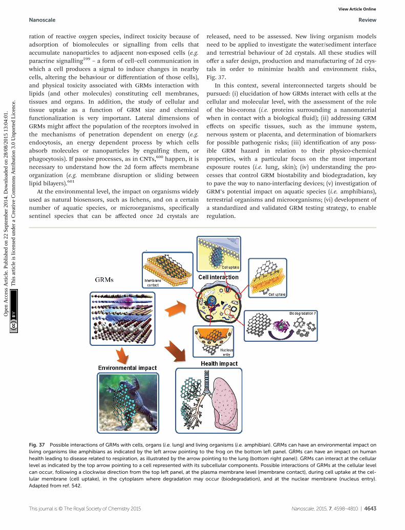
ration of reactive oxygen species, indirect toxicity because ofadsorption of biomolecules or signalling from cells thataccumulate nanoparticles to adjacent non-exposed cells (e.g.paracrine signalling599 – a form of cell–cell communication inwhich a cell produces a signal to induce changes in nearbycells, altering the behaviour or differentiation of those cells),and physical toxicity associated with GRMs interaction withlipids (and other molecules) constituting cell membranes,tissues and organs. In addition, the study of cellular andtissue uptake as a function of GRM size and chemicalfunctionalization is very important. Lateral dimensions ofGRMs might affect the population of the receptors involved inthe mechanisms of penetration dependent on energy (e.g.endocytosis, an energy dependent process by which cellsabsorb molecules or nanoparticles by engulfing them, orphagocytosis). If passive processes, as in CNTs,600 happen, it isnecessary to understand how the 2d form affects membraneorganization (e.g. membrane disruption or sliding betweenlipid bilayers).601
At the environmental level, the impact on organisms widelyused as natural biosensors, such as lichens, and on a certainnumber of aquatic species, or microorganisms, specificallysentinel species that can be affected once 2d crystals are
released, need to be assessed. New living organism modelsneed to be applied to investigate the water/sediment interfaceand terrestrial behaviour of 2d crystals. All these studies willoffer a safer design, production and manufacturing of 2d crys-tals in order to minimize health and environment risks,Fig. 37.
In this context, several interconnected targets should bepursued: (i) elucidation of how GRMs interact with cells at thecellular and molecular level, with the assessment of the roleof the bio-corona (i.e. proteins surrounding a nanomaterialwhen in contact with a biological fluid); (ii) addressing GRMeffects on specific tissues, such as the immune system,nervous system or placenta, and determination of biomarkersfor possible pathogenic risks; (iii) identification of any poss-ible GRM hazard in relation to their physico-chemicalproperties, with a particular focus on the most importantexposure routes (i.e. lung, skin); (iv) understanding the pro-cesses that control GRM biostability and biodegradation, keyto pave the way to nano-interfacing devices; (v) investigation ofGRM’s potential impact on aquatic species (i.e. amphibians),terrestrial organisms and microorganisms; (vi) development ofa standardized and validated GRM testing strategy, to enableregulation.
Fig. 37 Possible interactions of GRMs with cells, organs (i.e. lung) and living organisms (i.e. amphibian). GRMs can have an environmental impact onliving organisms like amphibians as indicated by the left arrow pointing to the frog on the bottom left panel. GRMs can have an impact on humanhealth leading to disease related to respiration, as illustrated by the arrow pointing to the lung (bottom right panel). GRMs can interact at the cellularlevel as indicated by the top arrow pointing to a cell represented with its subcellular components. Possible interactions of GRMs at the cellular levelcan occur, following a clockwise direction from the top left panel, at the plasma membrane level (membrane contact), during cell uptake at the cel-lular membrane (cell uptake), in the cytoplasm where degradation may occur (biodegradation), and at the nuclear membrane (nucleus entry).Adapted from ref. 542.
Nanoscale Review
This journal is © The Royal Society of Chemistry 2015 Nanoscale, 2015, 7, 4598–4810 | 4643
Ope
n A
cces
s A
rtic
le. P
ublis
hed
on 2
2 Se
ptem
ber
2014
. Dow
nloa
ded
on 2
8/08
/201
5 13
:04:
01.
Thi
s ar
ticle
is li
cens
ed u
nder
a C
reat
ive
Com
mon
s A
ttrib
utio
n 3.
0 U
npor
ted
Lic
ence
.View Article Online
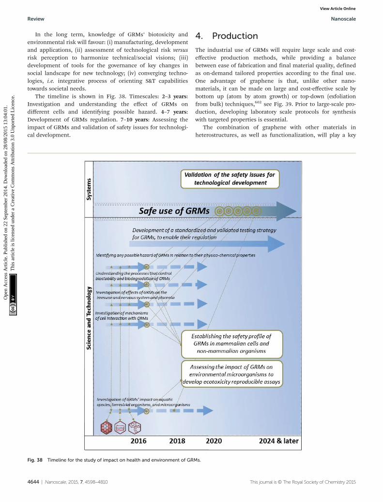
In the long term, knowledge of GRMs’ biotoxicity andenvironmental risk will favour: (i) manufacturing, developmentand applications, (ii) assessment of technological risk versusrisk perception to harmonize technical/social visions; (iii)development of tools for the governance of key changes insocial landscape for new technology; (iv) converging techno-logies, i.e. integrative process of orienting S&T capabilitiestowards societal needs.
The timeline is shown in Fig. 38. Timescales: 2–3 years:Investigation and understanding the effect of GRMs ondifferent cells and identifying possible hazard. 4–7 years:Development of GRMs regulation. 7–10 years: Assessing theimpact of GRMs and validation of safety issues for technologi-cal development.
4. Production
The industrial use of GRMs will require large scale and cost-effective production methods, while providing a balancebetween ease of fabrication and final material quality, definedas on-demand tailored properties according to the final use.One advantage of graphene is that, unlike other nano-materials, it can be made on large and cost-effective scale bybottom up (atom by atom growth) or top-down (exfoliationfrom bulk) techniques,602 see Fig. 39. Prior to large-scale pro-duction, developing laboratory scale protocols for synthesiswith targeted properties is essential.
The combination of graphene with other materials inheterostructures, as well as functionalization, will play a key
Fig. 38 Timeline for the study of impact on health and environment of GRMs.
Review Nanoscale
4644 | Nanoscale, 2015, 7, 4598–4810 This journal is © The Royal Society of Chemistry 2015
Ope
n A
cces
s A
rtic
le. P
ublis
hed
on 2
2 Se
ptem
ber
2014
. Dow
nloa
ded
on 2
8/08
/201
5 13
:04:
01.
Thi
s ar
ticle
is li
cens
ed u
nder
a C
reat
ive
Com
mon
s A
ttrib
utio
n 3.
0 U
npor
ted
Lic
ence
.View Article Online

role in validating GRMs as a disruptive nanotechnology plat-form for real-world devices. Table 2 summarize the state of theart in term of size and μ for some of the production strategiespresented in Fig. 39, together with targets applications.
The main targets are:• Development of scalable synthesis protocols that enable
tuning of electronic, structural and optical properties fordifferent applications.
Fig. 39 Schematic illustration of the main experimental setups for graphene production. (a) Micromechanical cleavage (b) Anodic bonding (c)Photoexfoliation. (d) Liquid phase exfoliation. (e) Growth from SiC. Schematic structure of 4H-SiC and the growth of graphene on SiC substrate.Gold and grey spheres represent Si and C atoms, respectively. At elevated temperatures, Si atoms evaporate (arrows), leaving a C-rich surface thatforms graphene. (f ) Precipitation from carbon containing metal substrate. (g) CVD process. (h) Molecular beam epitaxy. Different carbon sourcesand substrates (i.e. SiC, Si, etc.) can be exploited. (i) Chemical synthesis using benzene as building blocks. Adapted from ref. 602.
Table 2 State of the art (as of August 2014) of the main production approaches and foreseen applications
MethodCrystallitesSize, µm Sample Size, mm μ Applications
Micromechanicalcleavage
1000 1 2 × 105 cm2 V−1 s−1 Fundamental research and proof of principle devices106 cm2 V−1 s−1
(@T = 4 K)2 × 104 cm2 V−1 s−1
@RTLPE of graphite 0.01–1 0.1–1 100 cm2 V−1 s−1 Inks, coatings, paints, batteries, supercaps, solar cells,
fuel cells, composites, sensors, TCs, photonics, flexibleelectronics and optoelectronics, bio-applications
(∞ as overlapping flakes) (for a layer ofoverlapping flakes)@RT
LPE of GO >1 >1 1 cm2 V−1 s−1 Inks, coatings, paints, batteries, supercap, solar cells,fuel cells, composites sensors, TCs, photonics, flexibleelectronics and optoelectronics, bio-applications
(∞ as overlapping flakes) (for a layer ofoverlapping flakes)@RT
Growth on SiC 100 100 6 × 106 cm2 V−1 s−1 RF transistors(6″) @T = 4 K other electronic devices
CVD 50 000 1000 6.5 × 104 cm2 V−1 s−1 Photonics, nanoelectronics, TCs, sensors,bio-applications, flexible electronics@T = 1.7 K
3 × 104 cm2 V−1 s−1
@RT
Nanoscale Review
This journal is © The Royal Society of Chemistry 2015 Nanoscale, 2015, 7, 4598–4810 | 4645
Ope
n A
cces
s A
rtic
le. P
ublis
hed
on 2
2 Se
ptem
ber
2014
. Dow
nloa
ded
on 2
8/08
/201
5 13
:04:
01.
Thi
s ar
ticle
is li
cens
ed u
nder
a C
reat
ive
Com
mon
s A
ttrib
utio
n 3.
0 U
npor
ted
Lic
ence
.View Article Online
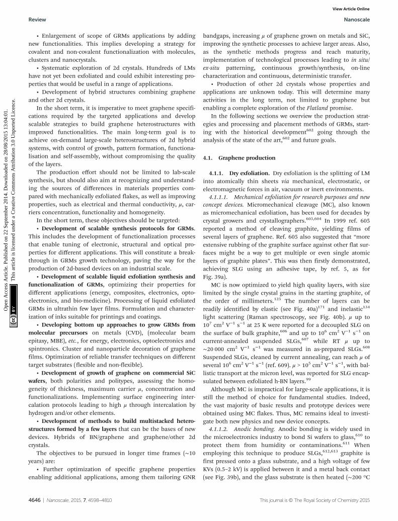
• Enlargement of scope of GRMs applications by addingnew functionalities. This implies developing a strategy forcovalent and non-covalent functionalization with molecules,clusters and nanocrystals.
• Systematic exploration of 2d crystals. Hundreds of LMshave not yet been exfoliated and could exhibit interesting pro-perties that would be useful in a range of applications.
• Development of hybrid structures combining grapheneand other 2d crystals.
In the short term, it is imperative to meet graphene specifi-cations required by the targeted applications and developscalable strategies to build graphene heterostructures withimproved functionalities. The main long-term goal is toachieve on-demand large-scale heterostructures of 2d hybridsystems, with control of growth, pattern formation, functiona-lisation and self-assembly, without compromising the qualityof the layers.
The production effort should not be limited to lab-scalesynthesis, but should also aim at recognizing and understand-ing the sources of differences in materials properties com-pared with mechanically exfoliated flakes, as well as improvingproperties, such as electrical and thermal conductivity, μ, car-riers concentration, functionality and homogeneity.
In the short term, these objectives should be targeted:• Development of scalable synthesis protocols for GRMs.
This includes the development of functionalization processesthat enable tuning of electronic, structural and optical pro-perties for different applications. This will constitute a break-through in GRMs growth technology, paving the way for theproduction of 2d-based devices on an industrial scale.
• Development of scalable liquid exfoliation synthesis andfunctionalization of GRMs, optimizing their properties fordifferent applications (energy, composites, electronics, opto-electronics, and bio-medicine). Processing of liquid exfoliatedGRMs in ultrathin few layer films. Formulation and character-ization of inks suitable for printings and coatings.
• Developing bottom up approaches to grow GRMs frommolecular precursors on metals (CVD), (molecular beamepitaxy, MBE), etc., for energy, electronics, optoelectronics andspintronics. Cluster and nanoparticle decoration of graphenefilms. Optimization of reliable transfer techniques on differenttarget substrates (flexible and non-flexible).
• Development of growth of graphene on commercial SiCwafers, both polarities and politypes, assessing the homo-geneity of thickness, maximum carrier μ, concentration andfunctionalizations. Implementing surface engineering inter-calation protocols leading to high μ through intercalation byhydrogen and/or other elements.
• Development of methods to build multistacked hetero-structures formed by a few layers that can be the bases of newdevices. Hybrids of BN/graphene and graphene/other 2dcrystals.
The objectives to be pursued in longer time frames (∼10years) are:
• Further optimization of specific graphene propertiesenabling additional applications, among them tailoring GNR
bandgaps, increasing μ of graphene grown on metals and SiC,improving the synthetic processes to achieve larger areas. Also,as the synthetic methods progress and reach maturity,implementation of technological processes leading to in situ/ex-situ patterning, continuous growth/synthesis, on-linecharacterization and continuous, deterministic transfer.
• Production of other 2d crystals whose properties andapplications are unknown today. This will determine manyactivities in the long term, not limited to graphene butenabling a complete exploration of the Flatland promise.
In the following sections we overview the production strat-egies and processing and placement methods of GRMs, start-ing with the historical development602 going through theanalysis of the state of the art,602 and future goals.
4.1. Graphene production
4.1.1. Dry exfoliation. Dry exfoliation is the splitting of LMinto atomically thin sheets via mechanical, electrostatic, orelectromagnetic forces in air, vacuum or inert environments.
4.1.1.1. Mechanical exfoliation for research purposes and newconcept devices. Micromechanical cleavage (MC), also knownas micromechanical exfoliation, has been used for decades bycrystal growers and crystallographers.603,604 In 1999 ref. 605reported a method of cleaving graphite, yielding films ofseveral layers of graphene. Ref. 605 also suggested that “moreextensive rubbing of the graphite surface against other flat sur-faces might be a way to get multiple or even single atomiclayers of graphite plates”. This was then firstly demonstrated,achieving SLG using an adhesive tape, by ref. 5, as forFig. 39a).
MC is now optimized to yield high quality layers, with sizelimited by the single crystal grains in the starting graphite, ofthe order of millimeters.125 The number of layers can bereadily identified by elastic (see Fig. 40a)171 and inelastic134
light scattering (Raman spectroscopy, see Fig. 40b). μ up to107 cm2 V−1 s−1 at 25 K were reported for a decoupled SLG onthe surface of bulk graphite,606 and up to 106 cm2 V−1 s−1 oncurrent-annealed suspended SLGs,607 while RT μ up to∼20 000 cm2 V−1 s−1 was measured in as-prepared SLGs.608
Suspended SLGs, cleaned by current annealing, can reach μ ofseveral 106 cm2 V−1 s−1 (ref. 609). μ > 105 cm2 V−1 s−1, with bal-listic transport at the micron level, was reported for SLG encap-sulated between exfoliated h-BN layers.99
Although MC is impractical for large-scale applications, it isstill the method of choice for fundamental studies. Indeed,the vast majority of basic results and prototype devices wereobtained using MC flakes. Thus, MC remains ideal to investi-gate both new physics and new device concepts.
4.1.1.2. Anodic bonding. Anodic bonding is widely used inthe microelectronics industry to bond Si wafers to glass,610 toprotect them from humidity or contaminations.611 Whenemploying this technique to produce SLGs,612,613 graphite isfirst pressed onto a glass substrate, and a high voltage of fewKVs (0.5–2 kV) is applied between it and a metal back contact(see Fig. 39b), and the glass substrate is then heated (∼200 °C
Review Nanoscale
4646 | Nanoscale, 2015, 7, 4598–4810 This journal is © The Royal Society of Chemistry 2015
Ope
n A
cces
s A
rtic
le. P
ublis
hed
on 2
2 Se
ptem
ber
2014
. Dow
nloa
ded
on 2
8/08
/201
5 13
:04:
01.
Thi
s ar
ticle
is li
cens
ed u
nder
a C
reat
ive
Com
mon
s A
ttrib
utio
n 3.
0 U
npor
ted
Lic
ence
.View Article Online

for ∼10–20 min).612,613 If a positive voltage is applied to thetop contact, a negative charge accumulates in the glass sidefacing the positive electrode, causing the decomposition ofNa2O impurities in the glass into Na+ and O2
− ions.612,613 Na+
moves towards the back contact, while O2− remains at the
graphite–glass interface, establishing a high electric field atthe interface. A few layers of graphite, including SLGs, stick tothe glass by electrostatic interaction and can then be cleavedoff;612,613 T and applied voltage can be used to control N andtheir size.612,613 Anodic bonding was reported to produceflakes up to ∼1 mm width.613 This method may also be usedfor other LMs.
4.1.1.3. Laser ablation and photoexfoliation. Laser ablationis the use of a laser beam to removal of material, via evapor-ation and/or sublimation, from a solid surface614, Fig. 39c). Inthe case of LMs, such as graphite, if the laser beam irradiationdoes not induce evaporation and/or sublimation of the carbonatoms, but the detachment of an entire or a part of a layer, theprocess is called photoexfoliation.615
Laser pulses can in principle be used to ablate/exfoliategraphite flakes, Fig. 39c. Tuning the energy density permitsthe accurate patterning of graphene.616 The ablation of adefined N can be obtained exploiting the energy densitywindows required for ablating a SLG616 and N-layer graphene
(NLGs).616 Ref. 616 reported that energy density increases fordecreasing N up to 7LG. Ref. 616 argued that the N depen-dence of the energy density is related to the coupling of heatwith NLGs via phonons, with the specific heat scaling as 1/N.For N > 7 the ablation threshold saturates.616 Laser ablation isstill in its infancy616,617 and needs further development. Theprocess is best implemented in inert or vacuum con-ditions,618,619 since ablation in air tends to oxidize the gra-phene layers.616 Promising results were recently demonstratedalso in liquids.620 Thus, photoexfoliation could be alternativeand complementary technique to LPE.
Laser irradiation has room for further optimization. Thistechnique was tested to produce flakes from direct laserirradiation of GO.621 New protocols are needed to prepare gra-phene flakes in liquid, overcoming the limitations of LPE,exploiting high boiling point solvents and surfactants. Thelaser irradiation approach is of general validity. It can beextended to other LMs with weak interlayer coupling, seesection 4.12.2.
4.1.2. Liquid phase exfoliation. Graphite can also be ex-foliated in liquid environments exploiting ultrasounds to extractindividual layers, Fig. 39d. The LPE process generally involvesthree steps: (1) dispersion in a solvent; (2) exfoliation; (3) “puri-fication”. The third step is necessary to separate exfoliated fromun-exfoliated flakes, and usually requires ultracentrifugation.Exfoliation can be done via chemical wet dispersion followed byultrasonication (Fig. 39d), both in aqueous250,624,625,627 andnon-aqueous solvents.35,622,623,625,626,629
The LPE yield can be defined in different ways. The yield byweight, YW [%], is the ratio between the weight of dispersedgraphitic material and that of the starting graphite flakes.35
The yield by SLG percentage, YM [%], is the ratio between thenumber of SLG and the total number of graphitic flakes in thedispersion.35 The Yield by SLG weight, YWM [%], is the ratiobetween the total mass of dispersed SLG and the total mass ofall dispersed flakes. YW does not give information on the“quality” (i.e. the composition of the dispersion, e.g. the pres-ence of SLG, BLG, etc.) of the dispersion, since it considersall the graphitic material (SLG, FLG and thicker flakes), thusit does not quantify the amount of SLG, but only the totalamount of graphitic material in dispersion. YM [%], andYWM [%] are more suitable to quantify the amount of dispersedSLGs.
In order to determine YW it is necessary to calculate theconcentration c [g L−1] of dispersed graphitic material. c isusually determined via optical absorption spectroscopy(OAS),35,58,624–627 exploiting the Beer–Lambert Law: A = αcl,where l [m] is the length of the optical path and α [L g−1 m−1]is the absorption coefficient. α can be experimentally deter-mined by filtering a known volume of dispersion, e.g. viavacuum filtration, onto a filter of known mass,35,624–627 andmeasuring the resulting mass using a microbalance. The fil-tered material is made up of graphitic flakes, surfactants orsolvents and residuals from the filter.35,624 Thermogravimetricanalysis (TGA) is used to determine the weight percentage ofgraphitic material, thus enabling the measurement of c.58–61
Fig. 40 (a) Optical micrograph of MC flake, with regions of differentthickness. (b) Evolution of Raman spectra with N.134 The spectra are nor-malized to have the same G peak intensity.602
Nanoscale Review
This journal is © The Royal Society of Chemistry 2015 Nanoscale, 2015, 7, 4598–4810 | 4647
Ope
n A
cces
s A
rtic
le. P
ublis
hed
on 2
2 Se
ptem
ber
2014
. Dow
nloa
ded
on 2
8/08
/201
5 13
:04:
01.
Thi
s ar
ticle
is li
cens
ed u
nder
a C
reat
ive
Com
mon
s A
ttrib
utio
n 3.
0 U
npor
ted
Lic
ence
.View Article Online

However, different values of α have been estimated both foraqueous59,60 and non-aqueous-based dispersions.35,626 Ref. 35derived α ∼ 2460 m L mg−1 m−1 for a variety of solvents,i.e. N-methylpyrrolidone, NMP, dimethylformamide, DMF,benzyl benzoate, γ-butyrolactone, GBL, etc., while later ref. 626reported α ∼ 3620 mL mg−1 m−1 for NMP. Ref. 624 gaveα ∼ 1390 mL mg−1 m−1 for aqueous dispersions with sodiumdodecylbenzene sulfonate (SDBS), while ref. 627 reported ahigher value ∼6600 mL mg−1 m−1, still for aqueous disper-sions but with sodium cholate (SC). Ref. 627 assigned thisdiscrepancy to the difference in concentration of the twodispersions. However, α cannot be dependent on the concen-tration (indeed it is used for its determination), thus morework is needed to determine its exact value.602
YM is usually determined via TEM and AFM. In TEM, N canbe counted both analyzing the edges134 of the flakes and byusing electron diffraction patterns.134 AFM enables the esti-mation of N by measuring the height of the deposited flakesand dividing by the graphite interlayer distance, 0.34 nm.602
However, the estimation for the height of SLG via AFM isdependent on the substrate.602 Indeed, on SiO2, a SLG has aheight of ∼1 nm,5 while on mica is ∼0.4 nm.628 Raman spectro-scopy can be used for the determination of YM
35,625,629 and toconfirm the results obtained with TEM and/or AFM. YWM [%]requires the estimation of the SLGs area other than N.35
Although this is more accurate (giving quantitative and quali-tative information on SLGs), with respect YW and YM, its deter-mination is time consuming. However, for a semi-quantitativeevaluation, YM and YW must be reported if YWM is not.
4.1.2.1. LPE of graphite. Ultrasound-assisted exfoliation iscontrolled by hydrodynamic shear-forces, associated with cavi-tation,630 i.e. the formation, growth, and collapse of bubbles orvoids in liquids due to pressure fluctuations.630 After exfolia-tion, the solvent–graphene interaction needs to balance theinter-sheet attractive forces.
Solvents ideal to disperse graphene are those that minimizethe interfacial tension [N m−1]631 between the liquid and gra-phene flakes. In general, interfacial tension plays a key rolewhen a solid surface is immersed in a liquid medium.631–633 Ifthe interfacial tension between solid and liquid is high, thereis poor dispersibility of the solid in the liquid.631 In the case ofgraphitic flakes in solution, if the interfacial tension is high,the flakes tend to adhere to each other and the cohesion (i.e.the energy per unit area required to separate two flat surfacesfrom contact631) between them is high, hindering their dis-persion in liquid.602 Liquids with surface tension (i.e. the prop-erty of the surface of a liquid that allows it to resist an externalforce, due to the cohesive nature of its molecules631) γ ∼40 mN m−1 (ref. 35), are the “best” solvents for the dispersionof graphene and graphitic flakes, since they minimize theinterfacial tension between solvent and graphene.602 The samesolvents have been investigated for the debundling ofCNTs.634–636
Ref. 637 determined via wettability and contact angle thesurface energy, ϱ [mJ m−2], of different graphitic materials,finding ϱ ∼ 46 mJ m−2, ∼55 mJ m−2, ∼62 mJ m−2 for RGO,
graphite and GO. The slight difference being due to thedifferent surface structure of GO, RGO and graphite. Ref. 638reported that the contact angle measurements are not affectedby N.
The majority of solvents with γ ∼ 40 mN m−1 (i.e. NMP,DMF, Benzyl benzoate, GBL, etc.) [see ref. 35 for a more com-plete list] have some disadvantages. E.g., NMP may be toxic forreproductive organs,639 while DMF may have toxic effects onmultiple organs.640 Moreover, all have high (>450 K) boilingpoints, making it difficult to remove the solvent after exfolia-tion. As an alternative, low boiling point solvents,641 such asacetone, chloroform, isopropanol, etc. can be used. Water, the“natural” solvent”, has γ ∼ 72 mN m−1,631 too high (30 mNm−1 higher than NMP) for the dispersion of graphene637 andgraphite.637 In this case, the exfoliated flakes can be stabilizedagainst re-aggregation by Coulomb repulsion using linearchain surfactants, e.g. SDBS,624 or bile salts, e.g. SC642 andsodium deoxycholate (SDC),250,625 or polymers, e.g. pluro-nic,643 etc. However, depending on application, surfactants/polymers may be an issue, e.g. compromising, decreasing,inter-flake conductivity.644
Thick flakes can be removed following different strategiesbased on ultracentrifugation in a uniform645 or density gradi-ent medium (DGM).646 The first is called differential ultra-centrifugation (sedimentation based-separation, SBS),645 whilethe second density gradient ultracentrifugation (DGU).646 SBSseparates various particles on the basis of their sedimentationrate645 in response to a centrifugal force acting on them. SBS isthe most common separation strategy and, to date, flakesranging from few nm to a few microns have been produced,with concentrations up to a few mg ml−1.626,647 High concen-tration is desirable for large-scale production of composites35
and inks.629 YM up to ∼70% can be achieved by mild soni-cation in water with SDC followed by SBS,250 while YM ∼ 33%was reported with NMP.629 This YM difference is related to thedifference in flake lateral size. In water-surfactant dispersionsflakes are on average smaller (∼30 nm250 to ∼200 nm624) thanin NMP (∼1 μm35,629), since the viscosity (ν) at RT of NMP(1.7 mPa s648) is higher than water (∼1 mPa s648). Larger flakesin a higher ν media experience a higher frictional force645,646
that reduces their sedimentation coefficient, making it moredifficult for them to sediment. This decreases YM in NMP com-pared to water.
Control on N is achieved via DGU: graphitic flakes are ultra-centrifuged in a preformed DGM646,649 see Fig. 41a,b. Duringthis process, they move along the cuvette, dragged by the cen-trifugal force, until they reach the corresponding isopycnicpoint, i.e., the point where their buoyant density equals that ofthe surrounding DGM.646 The buoyant density is defined asthe density (ρ) of the medium at the corresponding isopycnicpoint.649 Isopycnic separation has been used to sort CNTs bydiameter,650 metallic vs. semiconducting nature651, and chiral-ity.652 However, unlike CNTs of different diameter, graphiticflakes have the same density irrespective of N, so anotherapproach is needed to induce a density difference: coverage ofthe flakes with a surfactant results in an increase of buoyant
Review Nanoscale
4648 | Nanoscale, 2015, 7, 4598–4810 This journal is © The Royal Society of Chemistry 2015
Ope
n A
cces
s A
rtic
le. P
ublis
hed
on 2
2 Se
ptem
ber
2014
. Dow
nloa
ded
on 2
8/08
/201
5 13
:04:
01.
Thi
s ar
ticle
is li
cens
ed u
nder
a C
reat
ive
Com
mon
s A
ttrib
utio
n 3.
0 U
npor
ted
Lic
ence
.View Article Online
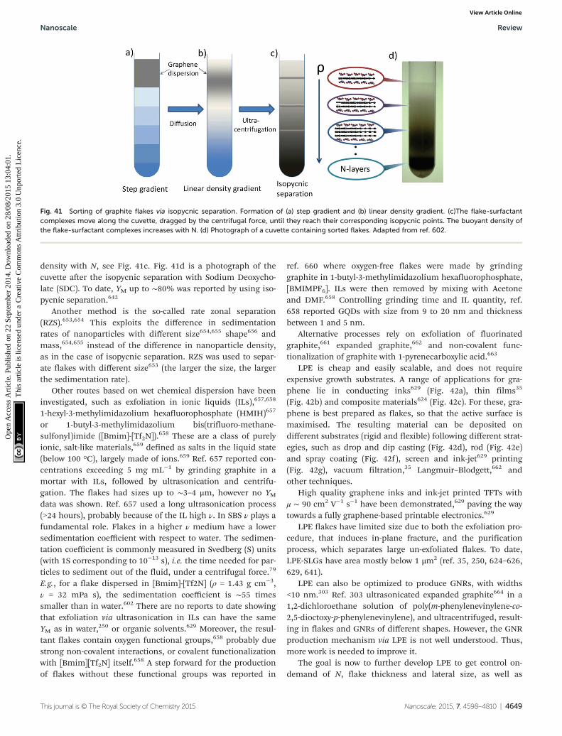
density with N, see Fig. 41c. Fig. 41d is a photograph of thecuvette after the isopycnic separation with Sodium Deoxycho-late (SDC). To date, YM up to ∼80% was reported by using iso-pycnic separation.642
Another method is the so-called rate zonal separation(RZS).653,654 This exploits the difference in sedimentationrates of nanoparticles with different size654,655 shape656 andmass,654,655 instead of the difference in nanoparticle density,as in the case of isopycnic separation. RZS was used to separ-ate flakes with different size653 (the larger the size, the largerthe sedimentation rate).
Other routes based on wet chemical dispersion have beeninvestigated, such as exfoliation in ionic liquids (ILs),657,658
1-hexyl-3-methylimidazolium hexafluorophosphate (HMIH)657
or 1-butyl-3-methylimidazolium bis(trifluoro-methane-sulfonyl)imide ([Bmim]-[Tf2N]).
658 These are a class of purelyionic, salt-like materials,659 defined as salts in the liquid state(below 100 °C), largely made of ions.659 Ref. 657 reported con-centrations exceeding 5 mg mL−1 by grinding graphite in amortar with ILs, followed by ultrasonication and centrifu-gation. The flakes had sizes up to ∼3–4 μm, however no YMdata was shown. Ref. 657 used a long ultrasonication process(>24 hours), probably because of the IL high ν. In SBS ν plays afundamental role. Flakes in a higher ν medium have a lowersedimentation coefficient with respect to water. The sedimen-tation coefficient is commonly measured in Svedberg (S) units(with 1S corresponding to 10−13 s), i.e. the time needed for par-ticles to sediment out of the fluid, under a centrifugal force.79
E.g., for a flake dispersed in [Bmim]-[Tf2N] (ρ = 1.43 g cm−3,ν = 32 mPa s), the sedimentation coefficient is ∼55 timessmaller than in water.602 There are no reports to date showingthat exfoliation via ultrasonication in ILs can have the sameYM as in water,250 or organic solvents.629 Moreover, the resul-tant flakes contain oxygen functional groups,658 probably duestrong non-covalent interactions, or covalent functionalizationwith [Bmim][Tf2N] itself.
658 A step forward for the productionof flakes without these functional groups was reported in
ref. 660 where oxygen-free flakes were made by grindinggraphite in 1-butyl-3-methylimidazolium hexafluorophosphate,[BMIMPF6]. ILs were then removed by mixing with Acetoneand DMF.658 Controlling grinding time and IL quantity, ref.658 reported GQDs with size from 9 to 20 nm and thicknessbetween 1 and 5 nm.
Alternative processes rely on exfoliation of fluorinatedgraphite,661 expanded graphite,662 and non-covalent func-tionalization of graphite with 1-pyrenecarboxylic acid.663
LPE is cheap and easily scalable, and does not requireexpensive growth substrates. A range of applications for gra-phene lie in conducting inks629 (Fig. 42a), thin films35
(Fig. 42b) and composite materials624 (Fig. 42c). For these, gra-phene is best prepared as flakes, so that the active surface ismaximised. The resulting material can be deposited ondifferent substrates (rigid and flexible) following different strat-egies, such as drop and dip casting (Fig. 42d), rod (Fig. 42e)and spray coating (Fig. 42f), screen and ink-jet629 printing(Fig. 42g), vacuum filtration,35 Langmuir–Blodgett,662 andother techniques.
High quality graphene inks and ink-jet printed TFTs withμ ∼ 90 cm2 V−1 s−1 have been demonstrated,629 paving the waytowards a fully graphene-based printable electronics.629
LPE flakes have limited size due to both the exfoliation pro-cedure, that induces in-plane fracture, and the purificationprocess, which separates large un-exfoliated flakes. To date,LPE-SLGs have area mostly below 1 μm2 (ref. 35, 250, 624–626,629, 641).
LPE can also be optimized to produce GNRs, with widths<10 nm.303 Ref. 303 ultrasonicated expanded graphite664 in a1,2-dichloroethane solution of poly(m-phenylenevinylene-co-2,5-dioctoxy-p-phenylenevinylene), and ultracentrifuged, result-ing in flakes and GNRs of different shapes. However, the GNRproduction mechanism via LPE is not well understood. Thus,more work is needed to improve it.
The goal is now to further develop LPE to get control on-demand of N, flake thickness and lateral size, as well as
Fig. 41 Sorting of graphite flakes via isopycnic separation. Formation of (a) step gradient and (b) linear density gradient. (c)The flake-surfactantcomplexes move along the cuvette, dragged by the centrifugal force, until they reach their corresponding isopycnic points. The buoyant density ofthe flake-surfactant complexes increases with N. (d) Photograph of a cuvette containing sorted flakes. Adapted from ref. 602.
Nanoscale Review
This journal is © The Royal Society of Chemistry 2015 Nanoscale, 2015, 7, 4598–4810 | 4649
Ope
n A
cces
s A
rtic
le. P
ublis
hed
on 2
2 Se
ptem
ber
2014
. Dow
nloa
ded
on 2
8/08
/201
5 13
:04:
01.
Thi
s ar
ticle
is li
cens
ed u
nder
a C
reat
ive
Com
mon
s A
ttrib
utio
n 3.
0 U
npor
ted
Lic
ence
.View Article Online

rheological (i.e., density, viscosity, and surface tension) pro-perties of the resulting dispersions. A combination of theoryand experiments is needed to fully understand the exfoliationprocess in different solvents, in order to optimise the separ-ation of flakes in centrifugal fields, so to achieve SLG and FLGwith well-defined morphological properties at a high rate.
A very desirable step is the development of techniquescapable of manipulating individual flakes. Optical tweezers(OT) can trap, manipulate, control and assemble dielectric par-ticles, single atoms, cells and nanostructures.250,665–669 Thesecan be used to trap graphene layers and/or GNRs in liquidenvironments. The coupling of OT with a Raman spectrometer(Raman Tweezers250), can test solutions composition and sortN in optofluidic channels. The assessment of exfoliation yieldis essential to allow further improvements. Detailed structuralcharacterisation of the exfoliated sheets can be done by aberra-tion-corrected HRTEM and STEM, electron energy loss spectro-
scopy (EELS) and in situ TEM. These can characterise theexfoliated materials down to the atomic level. The effect ofstructural defects on the electrical properties can also be inves-tigated in situ.
Ref. 670 reported a scalable method, based on shear mixingof graphite, Fig. 43. During rotation, the shear mixer acts as apump, pulling both liquid and solids into the mixing headwhere centrifugal forces drive them towards the edge of therotor/stator (see Fig. 43b).670 This is accompanied by intense(power density of ∼100 W l−1) shear as the materials are drivenbetween the rotor and screen and then out through the perfor-ations in the stator and into the main volume of the liquid.This method can produce ∼1.4 g h−1 of mostly FLG with YW =3.35% and could be applied to other LMs.670
4.1.2.2. LPE of graphite oxide. LPE is a versatile techniqueand can be exploited not only for the exfoliation of pristinegraphite, as reported in section 4.1.2.1, but also for the exfolia-
Fig. 42 (a) Graphene ink. (b) Graphene-based TCF and (c) graphene polymer composite. (d) Dip casting, (e) rod coating, (f ) spray and (g) inkjet print-ing of graphene inks.602
Review Nanoscale
4650 | Nanoscale, 2015, 7, 4598–4810 This journal is © The Royal Society of Chemistry 2015
Ope
n A
cces
s A
rtic
le. P
ublis
hed
on 2
2 Se
ptem
ber
2014
. Dow
nloa
ded
on 2
8/08
/201
5 13
:04:
01.
Thi
s ar
ticle
is li
cens
ed u
nder
a C
reat
ive
Com
mon
s A
ttrib
utio
n 3.
0 U
npor
ted
Lic
ence
.View Article Online

tion of graphite oxide and graphite intercalated compounds(GICs), which have different properties with respect to pristinegraphite,602 as discussed in this and the next section.
The oxidation of graphite in the presence of potassiumchlorate (KClO3) and fuming nitric acid was developed byBrodie in 1859 while investigating the reactivity of graphiteflakes.671 This process involved successive oxidative treatmentsof graphite in different reactors.671 In 1898, Staudenmaiermodified Brodie’s process by using concentrated sulphuricacid and adding KClO3 in successive steps during the reac-tion.672 This allowed carrying out the reaction in a singlevessel, streamlining the production process.673 However, bothmethods were time consuming and hazardous, as they alsoyielded chlorine dioxide (ClO2) gas,104 which can explosivelydecompose into oxygen and chlorine.674 Graphite oxide (GrO)flakes were already investigated by Kohlschtter and Haenniin 1918,675 and the first TEM images reported in 1948 byRuess and Vogt676 showed the presence of single sheets of GO.
In 1958, Hummers modified the process using a mixture ofsulphuric acid, sodium nitrate and potassium permanga-nate.677 Avoiding KClO3 made the process safer and quicker
with no explosive byproducts.677 These aggressive chemicalprocesses disrupt the sp2-bonded network and introducehydroxyl or epoxide groups,678–680 in the basal plane, whilecarbonyl and carboxylic groups, together with lactone, phenoland quinone attach to the edges (see Fig. 44). However, theintroduction of these functional groups is essential for the GOproduction and subsequent liquid dispersion.
GO flakes can be produced via sonication,303,681 stirring,682
thermal expansion,683 etc., of GrO. The aforementioned func-tional groups make them strongly hydrophilic, allowing theirdispersion in pure water,303,681 organic solvents,682,684 aqueousmixtures with methanol, acetone, acetonitrile685 or 1-propanoland ethylene glycol.686 However, although large GO flakes, upto several microns,687 can be produced, they are defective679
and insulating, with Rs ∼ 1012 Ω □−1(Ohm per square), orhigher.688
GO is luminescent under continuous wave irradiation.689
Visible excitation gives a broad PL spectrum from visible tonear-infrared,564 while blue emission690 is detected upon UVexcitation. This makes GO an interesting material for lightingapplications (e.g. light emitting devices691) and bio-imaging.564
Fig. 43 (a) Silverson model L5M high-shear mixer with mixing head in a 5 liters beaker of dispersion containing graphitic flakes. Close-up view of(b) mixing head (diameter = 32 mm) and (c) mixing head (diameter = 16 mm) with rotor (left) separated from stator. (d), bottles containing the finaldispersions. Adapted from ref. 670.
Fig. 44 GO synthesis and reduction. Graphite can be oxidized with different procedures in the presence of strong acids. The GO flakes have thebasal plane functionalized with epoxy and hydroxyl groups, both above and below it, and the edges with a variety of functional groups. This makesGO sheets defective. A partial restoration of the electronic properties is obtainable following different reduction strategies.602
Nanoscale Review
This journal is © The Royal Society of Chemistry 2015 Nanoscale, 2015, 7, 4598–4810 | 4651
Ope
n A
cces
s A
rtic
le. P
ublis
hed
on 2
2 Se
ptem
ber
2014
. Dow
nloa
ded
on 2
8/08
/201
5 13
:04:
01.
Thi
s ar
ticle
is li
cens
ed u
nder
a C
reat
ive
Com
mon
s A
ttrib
utio
n 3.
0 U
npor
ted
Lic
ence
.View Article Online
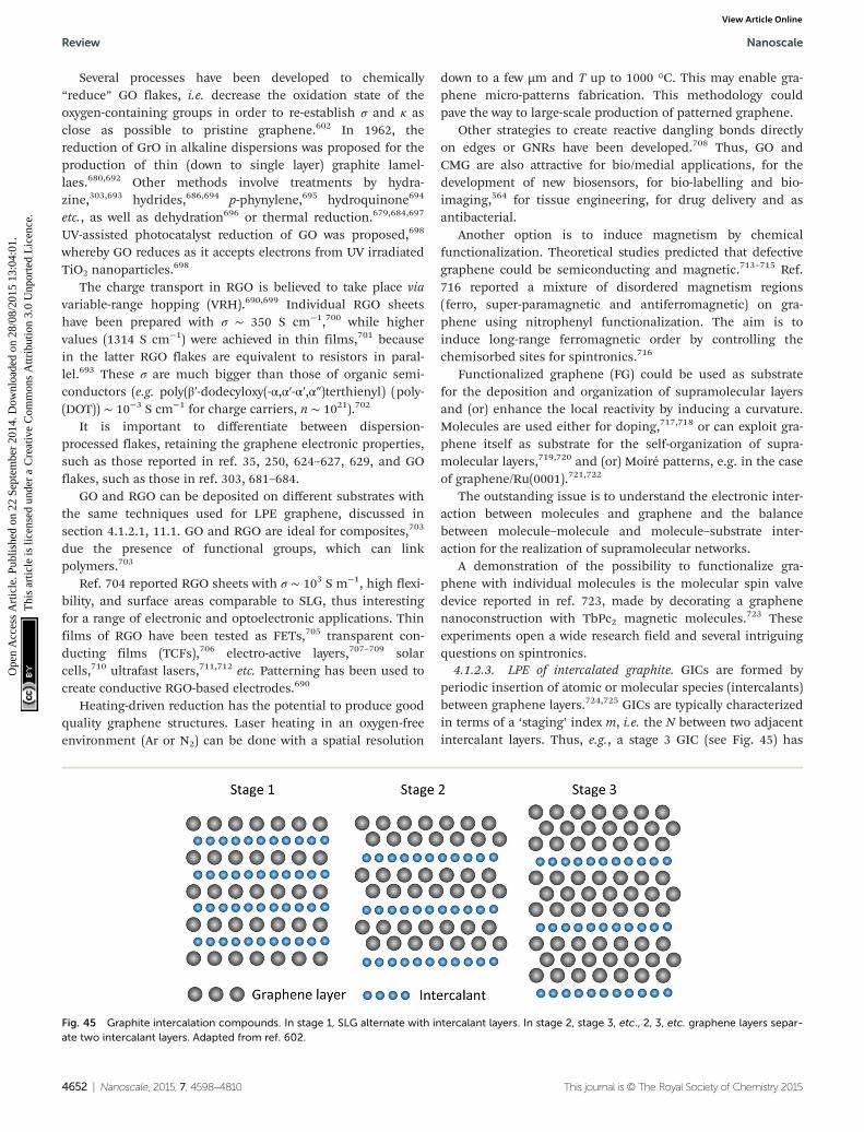
Several processes have been developed to chemically“reduce” GO flakes, i.e. decrease the oxidation state of theoxygen-containing groups in order to re-establish σ and κ asclose as possible to pristine graphene.602 In 1962, thereduction of GrO in alkaline dispersions was proposed for theproduction of thin (down to single layer) graphite lamel-laes.680,692 Other methods involve treatments by hydra-zine,303,693 hydrides,686,694 p-phynylene,695 hydroquinone694
etc., as well as dehydration696 or thermal reduction.679,684,697
UV-assisted photocatalyst reduction of GO was proposed,698
whereby GO reduces as it accepts electrons from UV irradiatedTiO2 nanoparticles.
698
The charge transport in RGO is believed to take place viavariable-range hopping (VRH).690,699 Individual RGO sheetshave been prepared with σ ∼ 350 S cm−1,700 while highervalues (1314 S cm−1) were achieved in thin films,701 becausein the latter RGO flakes are equivalent to resistors in paral-lel.693 These σ are much bigger than those of organic semi-conductors (e.g. poly(β′-dodecyloxy(-α,α′-α′,α″)terthienyl) (poly-(DOT)) ∼ 10−3 S cm−1 for charge carriers, n ∼ 1021).702
It is important to differentiate between dispersion-processed flakes, retaining the graphene electronic properties,such as those reported in ref. 35, 250, 624–627, 629, and GOflakes, such as those in ref. 303, 681–684.
GO and RGO can be deposited on different substrates withthe same techniques used for LPE graphene, discussed insection 4.1.2.1, 11.1. GO and RGO are ideal for composites,703
due the presence of functional groups, which can linkpolymers.703
Ref. 704 reported RGO sheets with σ ∼ 103 S m−1, high flexi-bility, and surface areas comparable to SLG, thus interestingfor a range of electronic and optoelectronic applications. Thinfilms of RGO have been tested as FETs,705 transparent con-ducting films (TCFs),706 electro-active layers,707–709 solarcells,710 ultrafast lasers,711,712 etc. Patterning has been used tocreate conductive RGO-based electrodes.690
Heating-driven reduction has the potential to produce goodquality graphene structures. Laser heating in an oxygen-freeenvironment (Ar or N2) can be done with a spatial resolution
down to a few µm and T up to 1000 °C. This may enable gra-phene micro-patterns fabrication. This methodology couldpave the way to large-scale production of patterned graphene.
Other strategies to create reactive dangling bonds directlyon edges or GNRs have been developed.708 Thus, GO andCMG are also attractive for bio/medial applications, for thedevelopment of new biosensors, for bio-labelling and bio-imaging,564 for tissue engineering, for drug delivery and asantibacterial.
Another option is to induce magnetism by chemicalfunctionalization. Theoretical studies predicted that defectivegraphene could be semiconducting and magnetic.713–715 Ref.716 reported a mixture of disordered magnetism regions(ferro, super-paramagnetic and antiferromagnetic) on gra-phene using nitrophenyl functionalization. The aim is toinduce long-range ferromagnetic order by controlling thechemisorbed sites for spintronics.716
Functionalized graphene (FG) could be used as substratefor the deposition and organization of supramolecular layersand (or) enhance the local reactivity by inducing a curvature.Molecules are used either for doping,717,718 or can exploit gra-phene itself as substrate for the self-organization of supra-molecular layers,719,720 and (or) Moiré patterns, e.g. in the caseof graphene/Ru(0001).721,722
The outstanding issue is to understand the electronic inter-action between molecules and graphene and the balancebetween molecule–molecule and molecule–substrate inter-action for the realization of supramolecular networks.
A demonstration of the possibility to functionalize gra-phene with individual molecules is the molecular spin valvedevice reported in ref. 723, made by decorating a graphenenanoconstruction with TbPc2 magnetic molecules.723 Theseexperiments open a wide research field and several intriguingquestions on spintronics.
4.1.2.3. LPE of intercalated graphite. GICs are formed byperiodic insertion of atomic or molecular species (intercalants)between graphene layers.724,725 GICs are typically characterizedin terms of a ‘staging’ index m, i.e. the N between two adjacentintercalant layers. Thus, e.g., a stage 3 GIC (see Fig. 45) has
Fig. 45 Graphite intercalation compounds. In stage 1, SLG alternate with intercalant layers. In stage 2, stage 3, etc., 2, 3, etc. graphene layers separ-ate two intercalant layers. Adapted from ref. 602.
Review Nanoscale
4652 | Nanoscale, 2015, 7, 4598–4810 This journal is © The Royal Society of Chemistry 2015
Ope
n A
cces
s A
rtic
le. P
ublis
hed
on 2
2 Se
ptem
ber
2014
. Dow
nloa
ded
on 2
8/08
/201
5 13
:04:
01.
Thi
s ar
ticle
is li
cens
ed u
nder
a C
reat
ive
Com
mon
s A
ttrib
utio
n 3.
0 U
npor
ted
Lic
ence
.View Article Online

each 3 adjacent graphene layers sandwiched by 2 intercalantlayers726 (the latter can also be more than 1 atom thick).
GICs have a long history since the first recorded productionby Schafhaeutl in 1840.724 Ref. 726, 727 summarized the his-torical development of GICs. The first determination of stageindex by X-ray diffraction was done in 1931 by Hoffman andFenzel.728 Systematic studies started in the late 1970s.
Intercalation of atoms or molecules with different m givesrise to a wide variety of electrical,726 thermal726 and magneticproperties.726 GICs have potential as highly conductivematerials.726,729–731 GICs with metal chloride or pentafluorideintercalants, such as antimony pentafluoride (SbF5) andArsenic pentafluoride (AsF5), received much interest sincethe 1970s.726,729–731 E.g., AsF5-GICs has slightly higher σ (6.3 ×10⁵ S cm−1)729 than bulk Cu730,731 (5.9 × 10⁵ S cm−1),729 whilethe graphite in plane σ is ∼4.5 × 10⁴ S cm−1.732 The σ increaseis assigned to injection of carriers from the intercalate layer,with low μ, to the graphite layers, with high μ.726
GICs can be superconducting733 with transition tempera-tures up to 11.5 K for CaC6 GICs at ambient pressure,734 andhigher with increasing pressure.735 Moreover, GICs are alsopromising for hydrogen storage, due to a larger interlayerspacing.736 GICs are already commercialized in batteries,737
in particular, in Li-ion batteries since the 1970s.738–740 GICshave also been used as negative electrodes (anode during dis-charge) in Li-ion batteries with the introduction of solidelectrolytes.741,742
The most common production strategies include two-zonevapour transport726,743,744 exploiting T differences betweengraphite and intercalants745 and, sometimes, the presence ofgases,745 e.g. Cl2 for intercalation of AlCl3.
726 GICs can be pro-duced in single (for binary or ternary GICs) or multiple steps,the latter when direct intercalation is not possible.746 Hun-dreds of GICs with donor (alkali, alkali earth metals, lantha-nides, metal alloys or ternary compounds, etc.) or acceptorintercalants (i.e. halogens, halogen mixtures, metal chlorides,acidic oxides, etc.) have been reported.726,744
The intercalation process increases the graphite interlayerspacing, especially for low stage index GICs,747,748 E.g., K, Rbor Cs-GICs have interlayer distance ∼0.53–0.59 nm, whilelarger intercalants, such as dimethylsulfoxide, give an inter-layer distance ∼0.9 nm,748 i.e. 1.5 to ∼3 times larger than the∼0.34 nm spacing in pristine graphite. This makes GICs prom-ising to produce graphene via LPE, even withoutultrasonication.628,747–750 However, although the exfoliationprocess is often called spontaneous,628,750 due to the absenceof ultrasonication, it requires mechanical energy, often pro-vided by stirring.628,750 To date it is possible to exfoliate GICswith lateral sizes ∼20 μm with YM ∼ 90%,749 and μ ∼ tens cm2
V−1 s−1.749
Note that many GICs tend to oxidize in air,726,751 andrequire a controlled ambient for their processing.726,751 This,coupled with the additional steps for GIC production, is one ofthe primary reasons why GICs are not yet extensively used toproduce graphene via LPE. However, ref. 752 recently reportedFeCl3 intercalated FLGs air-stable for up to one year.
Aspects of the intercalation mechanism, key for appli-cations, still need to be clarified. This has implications forlife duration of Li-ion batteries.753–755 The role of the solventand the search for novel strategies for intercalation are alsocrucial, particularly to achieve large quantities of LPE gra-phene. Some GICs were shown to be spontaneously soluble inpolar solvents without need of sonication or high shearmixing.628,750
Other open questions are: what is the role of the inter-calant, the charge transfer to the graphene layer and themodification of the graphene band structure.
4.2. Growth on SiC
The production of graphite from SiC, Fig. 39e, was reported byAcheson as early as 1896 (ref. 59) for lubricant applications.59
The growth mechanism has been investigated since the1960s.760 Both polar surfaces, the Si-terminated (0001) and theC-terminated (0001) surface, annealed at high T under UHVtend to graphitize, because of Si evaporation.756,757 Ref.758–760 reported the production of graphene films by thermaldecomposition of SiC above 1000 °C. This is not a self-limitingprocess and areas of different film thicknesses may exist.759
On the (0001)-surface (see Fig. 46) the graphene layer isgrown on top of a C-rich (6√3 × 6√3)R30° reconstruction withrespect to the SiC surface, called the buffer layer.761 This con-sists of C atoms arranged in a graphene-like honeycomb struc-ture,761 but without graphene-like electronic properties,because ∼30% are covalently bonded to Si.761
The buffer layer can be decoupled from the Si(0001)-face byhydrogen intercalation,763 becoming a quasi-free-standing SLGwith typical linear π bands.763 In contrast, the interactionbetween graphene and the C(0001)-terminated face is muchweaker.761
Growth of graphene on SiC is usually referred to as “epitax-ial growth”,764 even though there is a large lattice mismatchbetween SiC (3.073 Å) and graphene (2.46 Å) and the carbonrearranges itself in a hexagonal structure as Si evaporates fromthe SiC substrate, rather than being deposited on the SiCsurface, as would happen in a traditional epitaxial growthprocess. The term “epitaxy” derives from Greek, the prefix epimeans “over” or “upon” and taxis means “order” or “arrange-ment”. In 1928 Royer765 used the term “epitaxy” referring tothe “oriented growth of one substance on the crystal surface ofa foreign substance”. If the growing crystal and the substratehave the same lattice constants these are lattice matched.766
The use of “epitaxial” as the adjectival form of epitaxy hasbeen subjected to some criticism already in the sixties,because it is incorrect from the philological point of view.767
Epitactic is the correct form.767 In 1965 epitaxic was rec-ommended by ref. 768. However, the word “epitaxial” is nowwidely used and any attempt to change it is unrealistic.602 Wewill thus use “epitaxial” as adjectival form of epitaxy. There aretwo general epitaxial growth processes depending on the sub-strate, homo- and hetero-epitaxy. In the case of homoepitaxythe substrate is of the same composition and structure as thegrowing film, whereas in the case of heteroepitaxy the sub-
Nanoscale Review
This journal is © The Royal Society of Chemistry 2015 Nanoscale, 2015, 7, 4598–4810 | 4653
Ope
n A
cces
s A
rtic
le. P
ublis
hed
on 2
2 Se
ptem
ber
2014
. Dow
nloa
ded
on 2
8/08
/201
5 13
:04:
01.
Thi
s ar
ticle
is li
cens
ed u
nder
a C
reat
ive
Com
mon
s A
ttrib
utio
n 3.
0 U
npor
ted
Lic
ence
.View Article Online
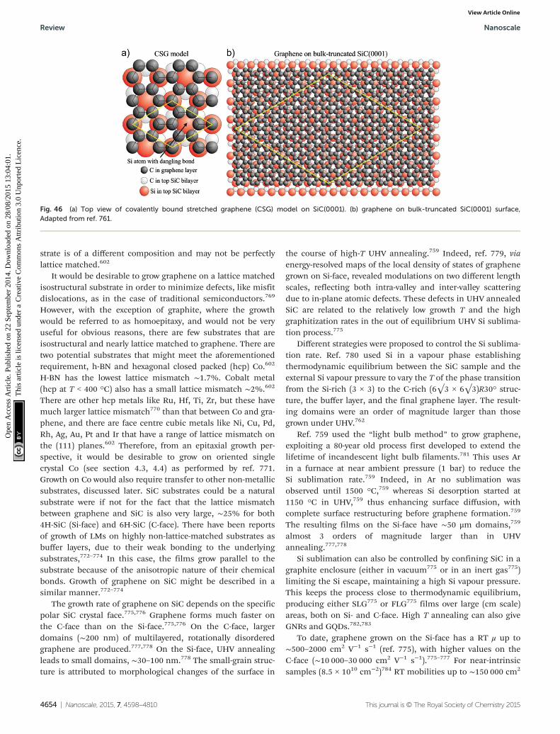
strate is of a different composition and may not be perfectlylattice matched.602
It would be desirable to grow graphene on a lattice matchedisostructural substrate in order to minimize defects, like misfitdislocations, as in the case of traditional semiconductors.769
However, with the exception of graphite, where the growthwould be referred to as homoepitaxy, and would not be veryuseful for obvious reasons, there are few substrates that areisostructural and nearly lattice matched to graphene. There aretwo potential substrates that might meet the aforementionedrequirement, h-BN and hexagonal closed packed (hcp) Co.602
H-BN has the lowest lattice mismatch ∼1.7%. Cobalt metal(hcp at T < 400 °C) also has a small lattice mismatch ∼2%.602
There are other hcp metals like Ru, Hf, Ti, Zr, but these havemuch larger lattice mismatch770 than that between Co and gra-phene, and there are face centre cubic metals like Ni, Cu, Pd,Rh, Ag, Au, Pt and Ir that have a range of lattice mismatch onthe (111) planes.602 Therefore, from an epitaxial growth per-spective, it would be desirable to grow on oriented singlecrystal Co (see section 4.3, 4.4) as performed by ref. 771.Growth on Co would also require transfer to other non-metallicsubstrates, discussed later. SiC substrates could be a naturalsubstrate were if not for the fact that the lattice mismatchbetween graphene and SiC is also very large, ∼25% for both4H-SiC (Si-face) and 6H-SiC (C-face). There have been reportsof growth of LMs on highly non-lattice-matched substrates asbuffer layers, due to their weak bonding to the underlyingsubstrates,772–774 In this case, the films grow parallel to thesubstrate because of the anisotropic nature of their chemicalbonds. Growth of graphene on SiC might be described in asimilar manner.772–774
The growth rate of graphene on SiC depends on the specificpolar SiC crystal face.775,776 Graphene forms much faster onthe C-face than on the Si-face.775,776 On the C-face, largerdomains (∼200 nm) of multilayered, rotationally disorderedgraphene are produced.777,778 On the Si-face, UHV annealingleads to small domains, ∼30–100 nm.778 The small-grain struc-ture is attributed to morphological changes of the surface in
the course of high-T UHV annealing.759 Indeed, ref. 779, viaenergy-resolved maps of the local density of states of graphenegrown on Si-face, revealed modulations on two different lengthscales, reflecting both intra-valley and inter-valley scatteringdue to in-plane atomic defects. These defects in UHV annealedSiC are related to the relatively low growth T and the highgraphitization rates in the out of equilibrium UHV Si sublima-tion process.775
Different strategies were proposed to control the Si sublima-tion rate. Ref. 780 used Si in a vapour phase establishingthermodynamic equilibrium between the SiC sample and theexternal Si vapour pressure to vary the T of the phase transitionfrom the Si-rich (3 × 3) to the C-rich (6√3 × 6√3)R30° struc-ture, the buffer layer, and the final graphene layer. The result-ing domains were an order of magnitude larger than thosegrown under UHV.762
Ref. 759 used the “light bulb method” to grow graphene,exploiting a 80-year old process first developed to extend thelifetime of incandescent light bulb filaments.781 This uses Arin a furnace at near ambient pressure (1 bar) to reduce theSi sublimation rate.759 Indeed, in Ar no sublimation wasobserved until 1500 °C,759 whereas Si desorption started at1150 °C in UHV,759 thus enhancing surface diffusion, withcomplete surface restructuring before graphene formation.759
The resulting films on the Si-face have ∼50 μm domains,759
almost 3 orders of magnitude larger than in UHVannealing.777,778
Si sublimation can also be controlled by confining SiC in agraphite enclosure (either in vacuum775 or in an inert gas775)limiting the Si escape, maintaining a high Si vapour pressure.This keeps the process close to thermodynamic equilibrium,producing either SLG775 or FLG775 films over large (cm scale)areas, both on Si- and C-face. High T annealing can also giveGNRs and GQDs.782,783
To date, graphene grown on the Si-face has a RT μ up to∼500–2000 cm2 V−1 s−1 (ref. 775), with higher values on theC-face (∼10 000–30 000 cm2 V−1 s−1).775–777 For near-intrinsicsamples (8.5 × 1010 cm−2)784 RT mobilities up to ∼150 000 cm2
Fig. 46 (a) Top view of covalently bound stretched graphene (CSG) model on SiC(0001). (b) graphene on bulk-truncated SiC(0001) surface,Adapted from ref. 761.
Review Nanoscale
4654 | Nanoscale, 2015, 7, 4598–4810 This journal is © The Royal Society of Chemistry 2015
Ope
n A
cces
s A
rtic
le. P
ublis
hed
on 2
2 Se
ptem
ber
2014
. Dow
nloa
ded
on 2
8/08
/201
5 13
:04:
01.
Thi
s ar
ticle
is li
cens
ed u
nder
a C
reat
ive
Com
mon
s A
ttrib
utio
n 3.
0 U
npor
ted
Lic
ence
.View Article Online
V−1 s−1 on C-face785 and ∼5800 cm2 V−1 s−1 on Si-face785
were reported. Ref. 100 reported an exceptionally high μ ina 40-nanometre-wide GNR grown on the (0001) face of SiC.These GNRs have shown ballistic conductance (at 4 K) on alength scale greater than ten micrometres with μ ∼ 6 × 106 cm2
V−1 s−1.100 This is equivalent to Rs ∼ 1 Ω □−1 (ref. 100).Graphene on SiC has the benefit that SiC is an established
substrate for power electronics.786 Top gated transistors havebeen fabricated from graphene on SiC on a wafer scale.787
High frequency transistors have also been demonstrated with100 GHz cut-off frequency788 higher than state-of-the-artSi transistors of the same gate length.433 Graphene on SiChas been developed as a resistance standard based onQHE.146,148,151
A drawback for this technology for large scale production isthe SiC wafers cost (∼$150–250 for 2″ wafer789 at 2011 prices,compared to ∼$5–10 for same size Si wafers) and their smallersize (usually no larger than 4″) compared to Si wafers. Oneapproach to reduce substrate costs is to grow thin SiC layers onsapphire, the latter costing less than ∼$10 for 2″ wafer,790 andsubsequently perform thermal decomposition to yield FLG.791
Thus far, FLGs produced in this way have inferior structuraland electronic quality compared to bulk SiC. Another approachis to grow SiC on Si.792 However SiC on Si is usuallycubic,793–795 making it challenging to achieve continuous highquality graphene, due to bowing and film cracking as a conse-quence of high residual stress.219,220,796,797 Ref. 798 grew SLGon 3C–SiC(111) with domains ∼100 μm2, combining atmos-pheric pressure growth759 with hydrogen intercalation,763
demonstrating that large domains can grow on 3C–SiC(111).Future challenges are the control on the layer thickness
homogeneity (currently not 100% monolayer)602 probably viabetter control of unintentional mis-cut angles, understandingand control of unintentional doping caused by the substrate,together with a better understanding of the effect of structuralin-homogeneities (e.g. steps, wrinkles, BLG inclusions) ontransport, and the mechanisms limiting μ. Other targets arethe growth of graphene on pre-patterned SiC substrates, and abetter control of growth on the SiC C-face, so to have SLG alsoon this face. The aim is also to tune the properties of graphenegrown on SiC via interface engineering (e.g. SiC surface hydro-genation, etc.) and better understanding of defects generatedduring growth and/or interface manipulation and identifi-cation of methods to heal them. Doping of graphene by inser-tion of heteroatoms needs also to be addressed, with the aimto have control on the procedures and consequently on theproperties of the graphene flakes. The achievement of many ofthe aforementioned goals will require a careful investigationand improvement of the substrates. A critical point to beaddressed is the transfer of SLG directly from a SiC surface toa target substrate, where the difficulty arises from the strongbinding of graphene to the SiC surface.761,775,776 This issuewas addressed by ref. 799 that developed a method in which afilm consisting of SLG or BLG grown on SiC is exfoliated viathe stress induced with a Ni film and transferred to anothersubstrate. Other points to be addressed are routes to improve
growth of cubic SiC as substrate, and the growth of insulatingSiC layers on cheap on-axis n-type substrates, in order toreplace expensive semi-insulating substrate materials.
The graphene quality and N are strongly dependent on thegrowth and annealing conditions. The advantage over stan-dard CVD is the graphene quality control achievable via tuningof carbon source thickness and annealing conditions. Inaddition, all the process steps occur in fully semiconductorcompatible environment. Thus, industry can then take benefitof the versatility of this method to integrate graphene in theirprocess flow. The long term goal is a totally controlled gra-phene nano-structuring, so to produce GNRs and GQDs ondemand. This is motivated by the prospect of band gap cre-ation in graphene.
4.3. Growth on metals by precipitation
Carbon can be deposited on a metal surface by a number oftechniques, e.g.: flash evaporation, physical vapour deposition(PVD), CVD, and spin coating. The carbon source can be asolid,800,801 liquid,802,892,803 or gas.849 In the case of a purecarbon source, flash evaporation804 or PVD805 can be used todeposit carbon directly on the substrate of interest, if non-carbide forming but with a finite carbon solubility, beforebefore diffusion at high T followed by precipitation of graphite(graphene) upon cooling. When the solid source is a polymer,it can be spun on the metal substrate at RT, followed by high Tannealing and growth.801
Segregation from carbon-containing metal and inorganicsubstrates is another approach to graphene growth,806–808 seeFig. 39f. The first reports of synthetic growth of graphite, i.e.not extracted from mined natural sources, on transition metalsdate back to the early 1940s.806–808 It was not until the 1970s,however, when the details of the growth process were eluci-dated. Ref. 809 identified, via a combination of Auger and low-energy electron diffraction (LEED), SLG formed from carbonprecipitation, following high T annealing of Co, Pt, or Ni. Thisprocess exploits the T-dependent solubility of interstitialcarbons in transition metals (i.e. Ni(111),810 Ru(001),811
Ir(111),812 Pt(111),813 Pd(100),813 etc.) or inorganic chemicalcompounds (i.e. LaB6
814 ) to achieve layer-by-layer growth ofgraphene on the surface. The amount of carbon that can bedissolved in most metals is up to a few atomic%.815
Materials for substrates are selected among those which donot form carbides, in order to eliminate the competitionbetween forming a carbide and graphite/graphene growth.Elements like Ti, Ta, Hf, Zr and Si, etc. form thermally stablecarbides, as shown by the phase diagram,816–820 thus are not“ideal” substrates for graphite/graphene growth. Moreover, allthese have a large (>20%) lattice mismatch with graphene. Thetransition metal is first annealed to high T (>1000 °C) in UHV,where the bulk solubility of interstitial carbon is high, thencooled to decrease solubility, resulting in its segregation as agraphene film.821
Graphite can also be obtained from carbon saturatedmolten iron during the formation of steel.822 In accordance tothe process just described, Fe is supersaturated with carbon,
Nanoscale Review
This journal is © The Royal Society of Chemistry 2015 Nanoscale, 2015, 7, 4598–4810 | 4655
Ope
n A
cces
s A
rtic
le. P
ublis
hed
on 2
2 Se
ptem
ber
2014
. Dow
nloa
ded
on 2
8/08
/201
5 13
:04:
01.
Thi
s ar
ticle
is li
cens
ed u
nder
a C
reat
ive
Com
mon
s A
ttrib
utio
n 3.
0 U
npor
ted
Lic
ence
.View Article Online

and the excess carbon precipitates.822 This is usually referredto as “Kish graphite”,823 derived from the German “Kies”, usedby steel workers to refer to the “mixture of graphite and slagseparated from and floating on the surface of molten pig ironor cast iron as it cools”.227
Significant attention has been devoted to the use of in-expensive metals such as Ni,824–826 and Co.827 Growth onnoble metals such as Ir,812 Pt,813 Ru,811 and Pd,813 aimed at abetter understanding of the growth mechanisms and/or atobtaining samples suitable for fundamental studies, e.g. forSTM,828 that require a conductive substrate. It would bedesirable in any case to have a stable metal that can promotegraphene single crystal growth, and the use of (111) orientedNi or Co could help in this sense, since they facilitate thehexagonal arrangement of carbon atoms.
The monolayer-graphite/graphite growth process on Ni wasfirst investigated in 1974 in ref. 809. SLG on Ni(111) wasobserved at T > 1000 K by Auger analysis, followed by graphiteformation upon cooling. During high T annealing, carbondiffuses into the metal until it reaches the solubility limit. Uponcooling, carbon precipitates forming first graphene, then graph-ite.809 The graphite film thickness depends on the metal, thesolubility of carbon in that metal, the T at which the carbon isintroduced, the thickness of the metal and the cooling rate.
To get large metal grains with crystalline orientation i.e.Ni(111),829 an annealing of the metal surface is often per-formed. Carbon segregation in Ni(111) was investigated inref. 830, 831 with control of number of surface C atoms byadjusting the annealing T.831
The graphene–metal distance and its nano-rippling on themetallic substrate determine the so-called graphene–metalMoiré superstructure.812,832 The latter is due to a mismatchbetween substrate and graphene lattice, and depends on themetal substrate. For lattice mismatches between graphene andsubstrate below 1%, commensurate superstructures, where theresulting broken symmetry is a doubling of the unit cell alongone axis (i.e. 1/2, 0, 0), are formed.833 This is the case forNi(111)821 and Co(0001).834 On the other hand, larger mis-matches yield incommensurate (total loss of symmetry in aparticular direction, i.e. (0.528,0,0)) moiré superstructures,such as in Pt(111),835 Ir(111),836 or Ru(0001)832,837 Indeed, gra-phene grown on Ir(111) yields flakes of well-defined orien-tation with respect to the substrate.812 On the contrary,graphene obtained via high-T segregation of C on Ru(0001)has a spread of orientations.837 Moreover, the graphene/Rulattice mismatch results in a distribution of tensile and com-pressive strains.838 This causes corrugation, due to buckling,and the formation of ∼1.7 Å humps.838 The Moiré superstruc-ture could be eliminated by the adsorption of oxygen on themetal surface acting as intercalant.839
Growth of graphene by precipitation requires carefulcontrol of the metal thickness, T, annealing time, cooling rate,and metal microstructure. Ref. 840 reported growth on Ni, Coand Ru on sapphire. Through the suppression of grain bound-aries, ref. 840 demonstrated uniform growth on Ru by asurface catalyzed reaction of hydrocarbons, but not on Ni and
Co.840 Both SLG and FLG were observed on Ni and Co, presum-ably due to the higher solubility of carbon and incorporationkinetics in comparison to Ru at the same T.840 However, ref.771 grew graphene on epitaxial Co on sapphire, achievingSLGs, in contrast to FLGs in ref. 840. An alternative strategy forSLG growth on high C solubility substrates was proposed byref. 841 using a binary alloy (Ni–Mo). The Mo component ofthe alloy traps all the dissolved excess C atoms, forming mol-ybdenum carbides and suppressing C precipitation.841 Gra-phene was also grown on Ru(0001) on sapphire.842
One of the shortcomings of the growth on metals is thatmost applications require graphene on an insulating substrate.Ref. 843 suggested that graphene can be grown directly onSiO2 by the precipitation of carbon from a Ni film depositedon the dielectric surface. This process has favourable perspec-tives but needs further refinement.
The aim of the work on graphene produced by carbon seg-regation is eventually to achieve a full control on graphenequality and N. These are strongly dependent on the growthand annealing conditions and a full control on the latter isstill missing. Deeply connected with this first issue are therequirements to obtain high quality graphene, where defectssuch as grain boundaries, pentagon–heptagon pairs, pointdefects,844 wrinkles,845 or local deformations are avoided orminimized. A further open issue is the transfer of grapheneproduced via carbon segregation onto arbitrary substrates anda process optimized for the various graphene applications stillrequires significant effort.
4.4. Chemical vapour deposition
Chemical vapour deposition is a process widely used todeposit or grow thin films, crystalline or amorphous, fromsolid, liquid or gaseous precursors of many materials. CVDhas been the workhorse for depositing materials used in semi-conductor devices for decades.846
The type of precursor is usually dictated by what is avail-able, what yields the desired film, and what is cost-effective forthe specific application. There are many different types of CVDprocesses: thermal, plasma enhanced (PECVD), cold wall, hotwall, reactive, and many more. Again, the type depends on theavailable precursors, the material quality, the thickness, andthe structure needed; cost is also an essential part of selectinga specific process.
The main difference in the CVD equipment for the differentprecursor types is the gas delivery system.847 In the case ofsolid precursors, the solid can be either vaporized and thentransported to the deposition chamber,847 or dissolved usingan appropriate solvent,847 delivered to a vaporizer,847 and thentransported to the deposition chamber.847 The transport of theprecursor can also be aided by a carrier gas.847 Depending onthe desired deposition temperature, precursor reactivity, ordesired growth rate, it may be necessary to introduce an exter-nal energy source to aid precursor decomposition.
One of the most common and inexpensive productionmethods is PECVD. The creation of plasma of the reactinggaseous precursors allows deposition at lower T with respect to
Review Nanoscale
4656 | Nanoscale, 2015, 7, 4598–4810 This journal is © The Royal Society of Chemistry 2015
Ope
n A
cces
s A
rtic
le. P
ublis
hed
on 2
2 Se
ptem
ber
2014
. Dow
nloa
ded
on 2
8/08
/201
5 13
:04:
01.
Thi
s ar
ticle
is li
cens
ed u
nder
a C
reat
ive
Com
mon
s A
ttrib
utio
n 3.
0 U
npor
ted
Lic
ence
.View Article Online

thermal CVD. However, since plasma can damage the growingmaterial, one needs to design the equipment and selectprocess regimes that minimize this damage. The details of thegrowth process are usually complex, and in many cases not allof the reactions are well understood. There are many differentways to perform plasma assisted CVD (see ref. 848 for an over-view). It is however important to match the equipment designwith the material one is trying to deposit and the precursorchemistry. Graphene should be simpler than multi-componentsystems, since it is a single element material. As with manyother materials, graphene growth can be performed using awide variety of precursors, liquids, gases, solids, growthchamber designs, thermal-CVD or PECVD, over a wide range ofchamber pressures and substrate T.
4.4.1. Thermal CVD on metals. In 1966 Karu and Beer849
exposed Ni to methane at T = 900 °C to form graphite, to beused as sample support for electron microscopy. In 1969,May850 reported that thermal decomposition of acetylene andethylene led to ring-like LEED patterns, as in the case ofcarbon on Pt, and that the material on the surface containedcarbon.850 His further analysis suggested that the ring-like pat-terns (polycrystalline) were due to rotationally disorderedgraphite.850 He also discussed the growth of monolayers,850 asthe first step to grow graphite, as revealed by X-ray diffraction.Thus, ref. 850 indicated the possibility of forming graphene onmetals by CVD. In 1971 ref. 851 observed the formation of FLGvia evaporation of C from a graphite rod.
In 1984 Kholin et al.852 grew graphene by CVD on Ir, tostudy the catalytic and thermionic properties of Ir in the pres-ence of carbon.853 Since then, other groups exposed metals,such as single crystal Ir833,854 to carbon precursors and studiedthe formation of graphitic films in UHV systems.
The first studies of graphene growth on metals were primar-ily focused on the understanding of the catalytic and thermio-nic activities of the metal surfaces in the presence of carbon.855
After 2004, the focus shifted to the actual growth of graphene.Low pressure chemical vapour deposition (LPCVD) on Ir(111)using an ethylene precursor was found to yield graphene struc-turally coherent even over the Ir step edges.833 While Ir can cer-tainly be used to grow graphene by CVD because of its lowcarbon solubility,815 it is difficult to transfer graphene to othersubstrates because of its chemical inertness. Ir is also expensive.Growth on Ni856 and Co827,857, metals compatible with Si pro-cessing since they have been used for silicides for over twodecades,858–862 and less expensive than Ir, poses a differentchallenge, i.e. FLGs are usually formed,825–827,849,854 and SLGsare non-uniform. Therefore, while many papers claim CVDgrowth at high T on Ni and Co,825–827,849,854 the process is infact carbon precipitation, not yielding uniform SLG, but ratherFLG films. The shortcoming of high solubility or expensiveand chemically unreactive metals motivated the search for aprocess and substrate that would be better suited to yield SLG.
The first CVD growth of uniform, large area (∼cm2) gra-phene on a metal surface was reported in 2009 by ref. 6 onpolycrystalline Cu foils, exploiting thermal catalytic decompo-sition of methane and low carbon solubility. This process is
almost self-limited, i.e. growth mostly ceases as soon as the Cusurface is fully covered with graphene, save ∼5% of the area,consisting of BLG and 3LG.6,863 Large area graphene growthwas enabled principally by the low C solubility in Cu,864 andCu mild catalytic activity.865
Growth of graphene on Cu by LPCVD was then scaled up in2010 by ref. 7, increasing the Cu foil size (30 inches), produ-cing films with μ ∼ 7350 cm2 V−1 s−1 at 6 K. Large grain,∼20–500 μm, graphene on Cu with μ ranging from ∼16 400 to∼25 000 cm2 V−1 s−1 at RT after transfer to SiO2 was reportedin ref. 866 and from ∼27 000 to ∼45 000 cm2 V−1 s−1 on h-BNat 1.6 K in ref. 867. There is now a huge effort towards theoptimization and the growth of high quality single crystal gra-phene by LPCVD. Ref. 868 synthesized large (∼4.5 mm2) singlecrystal hexagonal SLG domains on commercial polycrystallineCu foils, indicating the potential for large scale at low cost.The as synthesized graphene had μ ∼11 000 cm2 V−1 s−1 on aSiO2/Si substrate at RT. Ref. 869 by controlling surface oxygen,has repeatably grown centimeter-scale single-crystal graphenedomains. The μ measured for these single-crystal graphenesamples ranged from ∼40 000 to ∼65 000 cm2 V−1 s−1 at 1.7 Kand from ∼15 000 to ∼30 000 cm2 V−1 s−1 at RT. Since it is notpossible to measure the films while still on Cu, it is difficult todetermine if there is degradation as a result of transfer.
The current understanding of the growth mechanism is asfollows: carbon atoms, after decomposition from hydro-carbons, nucleate on Cu, and the nuclei grow into largedomains.866,870 The nuclei density is principally a function ofT and pressure and, at low pressure, mTorr, and T > 1000 °C,very large single crystal domains, up to ∼1 cm 869 are observed.However, when the Cu surface is fully covered, the filmsbecome polycrystalline, since the nuclei are not regis-tered,6,865,868,870 i.e. they are mis-oriented or incommensuratewith respect to each other, even on the same Cu grain.This could be ascribed to the low Cu–C binding energy.871
It would be desirable to have substrates with higher bind-ing energy with C.871 However, while Ru is compatible withSi processing,872 oriented Ru films may be difficult to grow onlarge (300–450 mm) Si wafers, or transferred from othersubstrates.
Graphene nucleation needs to be investigated, to controland enhance domain size, via controlled and multi-stepexposures. Basic reaction kinetics and layer-by-layer growthneed to be investigated by dedicated surface science experi-ments. Real-time spectroscopy could in principle be of greathelp to monitor CVD-graphene growth and understand thick-ness distribution as well as optimize the growth conditions.Cu pre-treatments, electrochemical polishing,873,874 and high-pressure annealing868 are shown to be critical for suppressinggraphene nucleation site density. Electrochemical polish-ing873,874 cleans the Cu surface and removes the impuritylayer.
There are some difficult issues to deal with when growinggraphene on most metal substrates, especially Cu, because ofthe difference in thermal expansion coefficient between Cuand graphene, of about an order of magnitude.875 The thermal
Nanoscale Review
This journal is © The Royal Society of Chemistry 2015 Nanoscale, 2015, 7, 4598–4810 | 4657
Ope
n A
cces
s A
rtic
le. P
ublis
hed
on 2
2 Se
ptem
ber
2014
. Dow
nloa
ded
on 2
8/08
/201
5 13
:04:
01.
Thi
s ar
ticle
is li
cens
ed u
nder
a C
reat
ive
Com
mon
s A
ttrib
utio
n 3.
0 U
npor
ted
Lic
ence
.View Article Online
mismatch gives rise to a significant wrinkle density uponcooling.863 These wrinkles are defective, as determined byRaman spectroscopy,866 and may also cause significant devicedegradation through defect scattering, similar to the effectof grain boundaries on μ in semiconducting materials.866
These defects however, may not be detrimental for many non-electrically-active applications, such as transparent electrodes.Perhaps one could use relatively cheaper substrates suchas Cu (Cu is cheaper than Ir, Ru, Pt) and use an electro-chemical process to remove graphene while reusing Cu, sothat the cost is amortized over many growth runs. Becauseof some unattractive properties (e.g. surface rougheningand sublimation) of Cu at the current thermal CVD growthT > 1000 °C, the community has been searching for new sub-strates that take advantage of the self-limited growth process,in addition to dielectrics. Ref. 876 reported growth of SLG onNi(111) at lower T, 500–600 °C, using ethylene by UHV CVD,and identified the process as self-limiting, presumably due tothe low C solubility in Ni at T < 650 °C.877 However, the Trange within which graphene can be grown on Ni is narrow,100 °C,876 and could result in a Ni2C phase,876 which can giverise to defects in the Ni crystal. Thus one could surmise thatany graphene could be non-uniform across the Ni–Ni2Cregions.
Graphene was also grown on Cu by exposing it to liquids orsolid hydrocarbons.801,878 Ref. 878 reported growth usingbenzene in the T range 300–500 °C.
The presence of the substrate generally modifies the gra-phene electronic properties, thus it is of paramount impor-tance to optimize the interaction between graphene andsubstrate. This can be tuned by applying surface treatmentsthat, in turn, can provide additional control on the grapheneproperties. E.g., substrates and interfacial dielectrics with opti-mized properties would enable high μ devices.
The process space for SLG-CVD growth is very wide anddepends on many factors, from substrate choice, to specificgrowth conditions, as well as variables not under directcontrol. It is critical to know the material requirements forspecific applications, so that one can tune the growth process/conditions to the application. Growth of graphene on singlecrystal substrates would be a desired route for improving elec-tronic properties. Following the growth of graphene on Cu,ref. 879 developed a Co deposition process to form highlycrystalline Co on c-plane sapphire where they grew SLG by CVDat high T. However, they did not distinguish between facecentred cubic (fcc)(111)Co and hcp(0002)Co and did notcomment on potential phase transformation issues at T lowerthan the fcc to hcp phase transition (∼400 °C). While thisprocess may seem incompatible with Si processing, and thematerial cost could be high, it is important to learn how totake advantage of processes that enable growth of higherquality graphene on stable surfaces, not necessarily singlecrystals.
Another question is: can we controllably grow FLGs? Cata-lytic decomposition of CO on various metals, such as Fe, Cu,Ag, Mo, Cr, Rh, and Pd, was studied by Kehrer and Leidheiser
in 1954.808 They detected graphitic carbon on Fe after exposureto CO for several hours at 550 °C, but found the other metalsto be inactive. The presence of BLG and TLG on Cu6 poses thequestion of the growth process for these isolated regions, sinceat first one would like to grow uniformly SLG. Growth of con-trolled Bernal stacked films is not easy, but small regions havebeen observed.880 Ref. 880 reported homogenous BLG by CVDon Cu. However, it not clear whether the films are of highenough quality for high performance electronic devices, sinceref. 880 did not map the D peak, and μ was ∼580 cm2 V−1 s−1
at RT.Another approach was proposed by ref. 881 by increasing
the solubility of C in Cu via a solid solution with Ni, formingthe binary alloy, Cu–Ni. By controlling Ni percentage, filmthickness, solution T, and cooling rate, N was controlled,enabling BLG growth.881
Graphene films with size ∼50 cm and μ > 7000 cm2 V−1 s−1
were produced on Cu and transferred via a R2R process, seeFig. 47.7 The goal is now to grow high quality samples (withcrystal size >1 mm) over large areas via R2R. Low pressurethermal CVD synthesis and a direct R2R transfer using photo-curable epoxy resin was used to fabricate a 100 m-long gra-phene transparent conductive film (GTCF) with a Rs as low as150 Ω □−1.882
Among the many areas that still need to be explored,growth on metallic alloys need yet to be investigated, theoptimisation of CH4–H2–Ar mixtures has yet to be done, andthe same can be said about testing and screening of alternativeprecursors. So far there is also little experimental insight intothe underlying GB formation mechanisms, crucial to under-stand and control charge propagation across/within these line-defects. On one hand, there is a need for quick and easycharacterization methods, able to reveal the grain structure ofthe CVD samples.883 On the other hand, GBs can be highlytransparent,884 as well as perfectly reflective,884 and areexpected to act as molecular metallic wires885 or filter the pro-pagating charge carriers based on the valley-index.886 In orderto explore and exploit these properties, the investigation ofthe electronic properties of individual GBs with knownatomic configuration is needed. STM is a versatile tool forinvestigating the structure of individual GBs at atomic resolu-tion and their electronic (and magnetic) properties on the nmscale.307
Growth of graphene on single crystal substrates is anotherroute towards the improvement of its electronic properties,although the high cost of such substrates makes them lesssuitable for large-scale applications. This requires in situgrowth monitoring. TEM will be fundamental to obtain atomicimages of domain boundaries, as well as macroscopic imagesof the relative domain orientations in a film.241
Reducing the growth T is desirable in order to cut pro-duction costs, and directly integrate graphene with standardCMOS processing. Growth of FLG at 650 °C was demonstratedon Fe.887 However, the optimization of layer control andgrowth T below 450 °C is required for CMOS integration.Although the growth of graphene at 325 °C was shown on
Review Nanoscale
4658 | Nanoscale, 2015, 7, 4598–4810 This journal is © The Royal Society of Chemistry 2015
Ope
n A
cces
s A
rtic
le. P
ublis
hed
on 2
2 Se
ptem
ber
2014
. Dow
nloa
ded
on 2
8/08
/201
5 13
:04:
01.
Thi
s ar
ticle
is li
cens
ed u
nder
a C
reat
ive
Com
mon
s A
ttrib
utio
n 3.
0 U
npor
ted
Lic
ence
.View Article Online

MgO,888 its suitability for applications is yet to be elucidated.Graphene grown on Cu foils at T as low as 300 °C usingbenzene as a precursor was also reported.889
MWCVD has also been proposed as a method for graphenegrowth.890,891 Ref. 891 reported growth at 150–300° C. However,to date SLG grown has not yet been demonstrated, with thedeposited films consisting of sub-micrometer flakes.891 Never-theless, this approach was successfully used for the productionof TCs.891 With further developments it could be a viable strat-egy for large scale, low T graphene production.891
A key target is thus the development of low T growth onlarge area, by understating and optimising plasma chemistry.
Low-T, high-density pulsed micro wave plasmas (electrondensity close to 1012 cm−3 ) are not only usable for large areagrowth, but also for surface processing and work-functionengineering, important for chemical functionalization, and forμ control. Systems scalable to large areas should beinvestigated.
The production of unsupported flakes using alcohols ascarbon feedstock was also demonstrated,892,893 with the poten-tial for up-scaling. The target is to further up-scale the CVD-growth, developing a protocol for a batch reactor, producingm2-sized graphene.
The development of new routes to achieve stable doping isanother key need for commercialization. Different approachesare to be investigated, either during growth, by exploitingalternative precursors (i.e. pyridine), or post-growth, via “mole-cular doping” by stable hydrazil- and nitroxide- radicals andmetal grids.
The growth of graphene on non-flat substrates such as, e.g.,Cu wires or corrugated Cu substrates instead of flat Cu films,is an area to be investigated that could open new applicationsboth in electronics, energy and catalysis.
Another key point is the development of reliable, fast, econ-omic and environmentally friendly transfer techniques.Methods for the recovery of the metal substrates are alsoneeded for cost reduction and environmental issues.
4.4.2. CVD on semiconductors and insulators. Electronicapplications require graphene grown, deposited or transferredonto dielectric surfaces. Growth of high-quality graphenelayers on insulating substrates, such as SiO2, SiC, sapphire,etc., would be a major step forward towards the applications innano-electronics. The use of SiC wafers in microelectronics isbecoming increasingly popular894 (see, e.g., the new SiCMOSFET developed by CREE894) which should result in lower-ing of their prices. SiC substrates of up to 150 mm diametershould become available in the short term.
CVD of carbon thin films on insulators has been knownsince 1971.895 However, thus far, it was optimized to givehighly sp3 bonded diamond-like carbons.199 Recently thisapproach was developed to achieve graphitic films.896,897
Growth of high-quality graphene on insulating substrates,such as SiO2, high-K dielectrics, h-BN, etc. would be ideal forelectronics. There have been many attempts to grow on SiC,898
sapphire899 and Si3N4/Si,900 as well as on metal oxides such as
MgO,888 and ZrO2.901 However, while graphitic regions are
observed at T < 1000 °C, none of the processes yield, to date,planar SLG films covering the whole surface.899 Thus far, thebest quality was achieved on sapphire899 (3000 cm2 V−1 s−1
and 10 500 cm2 V−1 s−1 at RT and 2 K, respectively).h-BN was shown to be effective as a substrate for graphene
CVD,902–905 and graphene produced by this method appearscomparable to that grown on transition metal catalysts833,906
with promise for hetero-epitaxial growth of heterostructures(e.g. graphene/h-BN). As well as achieving direct growth on aninsulator, this approach has the additional benefit of an atom-
Fig. 47 Roll-based production of graphene. (a) Schematic of the process. (b) A Cu foil is wrapped on a 7.5 inch quartz tube, then placed into an8-inch quartz reactor. (c) R2R transfer of graphene from to a Polyethylene terephthalate (PET) film.7
Nanoscale Review
This journal is © The Royal Society of Chemistry 2015 Nanoscale, 2015, 7, 4598–4810 | 4659
Ope
n A
cces
s A
rtic
le. P
ublis
hed
on 2
2 Se
ptem
ber
2014
. Dow
nloa
ded
on 2
8/08
/201
5 13
:04:
01.
Thi
s ar
ticle
is li
cens
ed u
nder
a C
reat
ive
Com
mon
s A
ttrib
utio
n 3.
0 U
npor
ted
Lic
ence
.View Article Online
ically smooth substrate, comparable with diamond-like carbon(DLC) surfaces,907 with few dangling bonds and chargetraps.908 Direct growth of graphene/h-BN stacks, by both CVDand metal–organic CVD (MOCVD), is the ideal alternative totedious successive exfoliations of rare BN single crystals(mostly one source in Japan909). CVD can also give c-BN com-posite layers with various topologies.910 Different B and N pre-cursors (solid, liquid, gaseous) should be tested in a variety ofenvironments, aiming at optimum quality and layer control,and privileging less costly and harmful ones. Wafer scaleextension of BN/graphene encapsulation techniques wouldpave the way to transport in high-frequency electronics,788 aregime exploiting Dirac Fermion optics, with no counterpart insemiconductor electronics. Substrate tailoring may optimizethese properties in a broad (and economically relevant) spec-trum, from microwave to optics, including millimeter waves(THz) and IR. The aim is to produce graphene on smart sub-strates in a single CVD run. At present, however, only FLGswere grown by CVD on h-BN, thus improved thickness controlis needed. Understanding basic growth processes is needed,with the help of both in situ and ex situ characterizations.These procedures need to be adapted to more scalableconditions.
As mentioned above, growth of single crystal graphene ondielectric surfaces is highly desirable, but to date the crystalsize on dielectrics is limited to micron size.911 Ref. 912reported the growth of single crystal monolayer graphene ongermanium. The authors took advantage of the low (108–1010
cm−3)913 solubility of C in Ge as in the case of C in Cu to growsingle crystal graphene on hydrogen-terminated Ge(110). Theyobserved a low wrinkle density, and assigned it to the lowthermal expansion coefficient difference between grapheneand Ge.912 Due to the small (∼60 meV)914 binding energybetween graphene and Ge, ref. 912 were able to mechanicallyexfoliate graphene using an Au film carrier, minimizing thedefects usually created using organic material transfermethods. This is a major advance, although nucleation andsurface flatness may still require optimization.
4.4.3. Plasma enhanced CVD. Plasma-enhanced CVD(PECVD) is a scalable and cost effective large area depositiontechnique, with numerous applications ranging from elec-tronics (IC, interconnects, memory and data storage devices),to flexible electronics7 and photovoltaic.915 PECVD’s strengthrelies in the potential of synthesizing graphene at lower T thanconventional CVD in a graphene-on-insulator environment.This comes useful in multiple applications, especially whenconsidering the process for CMOS devices.
The use of plasmas to reduce T during growth/depositionwas extensively exploited in the growth of nanotubes,916–923
and amorphous carbon.200–203,924–926 In 1998 ref. 316 reportedSLG with a curved structure as a byproduct of PECVD ofdiamond-like carbon. A number of other groups later reportedgrowth of vertical SLG925 and FLG,919,924,926–929 by microwavePECVD on several substrates, including non-catalytic, carbideforming substrates, such as SiO2. SLGs and FLGs nucleate atthe surface, but then continue to grow vertically, perhaps
because of the high concentration of carbon radicals,891 thusresulting in high growth rate. This material is promising forsupercapacitors or other applications, such as FE, not requir-ing planar films.
Graphene was grown by PECVD using methane at T as lowas 500 °C,930 but the films had a significant D-band, thus withquality still not equivalent to exfoliated or thermal CVD gra-phene.891,930 Nevertheless, ref. 891 demonstrated that growthmay be carried out at low T, and the material may be usedfor applications without the stringent requirements of elec-tronics. E.g., ref. 891 used PECVD at 317 °C to make TCs withRs ∼ 2 kΩ □−1 at Tr ∼ 78%.
PECVD might address the key issue of growth at low T,in order to prepare graphene directly on substrates com-patible with applications and processing technologies listedabove, e.g. direct deposition on plastic. The advantage ofplasma methods with respect to thermal CVD, is the pro-duction of graphitic materials without metal catalyst over awide range of growth conditions, both surface-bound andfreestanding.917
However, large domains are needed, together with areduction of damage caused by direct plasma during growth,that might limit the quality of graphene that can be achievedwith this approach. Nevertheless, this approach seems to bepromising for TCs.7
Inductively coupled plasma (ICP) CVD, (where the depo-sition pressure and the applied power to the plasma are con-trolled from two radio frequency-generators; one connected tothe ICP-source, the other to the substrate931) was also used togrow graphene on 150 mm Si,931 achieving uniform films andgood transport properties (i.e. μ up to ∼9000 cm2 V−1 s−1). Thisprocess is still under development with insufficient data onthe structure of the material.
The long term target plan (>10 years) is to achieve on-demand graphene deposition on insulator/Si and othermaterials on 300–450 mm wafer size, in-line with the fabrica-tion projections in the electronic industry. The challenge is todevelop an integrated ALD-PECVD process that would allowdeposition of compatible insulators at the same time assynthesising graphene. This should be done without compro-mising the quality of the graphene layer.
4.5. Molecular beam epitaxy growth of graphene oninsulating surfaces
MBE is a UHV-based technique for producing high quality epi-taxial structures with monolayer control.932 Since its introduc-tion in the 1970s932 as a tool for growing high-puritysemiconductor films, MBE has evolved into one of the mostwidely used techniques for epitaxial layers of metals, insula-tors and superconductors, both at the research and the indus-trial level. MBE of single crystal semiconductors, e.g. GaAs, iswell-established and has produced hetero-junctions with thecurrent record μ (3.5 × 107 cm2 V−1 s−1 (ref. 933)). MBE hasalso produced record low threshold current density multi-quantum-well lasers.934 MBE can achieve precise control ofboth the chemical composition and the doping profile. MBE
Review Nanoscale
4660 | Nanoscale, 2015, 7, 4598–4810 This journal is © The Royal Society of Chemistry 2015
Ope
n A
cces
s A
rtic
le. P
ublis
hed
on 2
2 Se
ptem
ber
2014
. Dow
nloa
ded
on 2
8/08
/201
5 13
:04:
01.
Thi
s ar
ticle
is li
cens
ed u
nder
a C
reat
ive
Com
mon
s A
ttrib
utio
n 3.
0 U
npor
ted
Lic
ence
.View Article Online
can use a wide variety of dopants compared to CVD epitaxialtechniques.
MBE can be used to grow carbon films (see Fig. 39h)directly on Si(111),935 and is a promising approach to achievehigh-purity graphene heterostructures on a variety of sub-strates, such as SiC, Al2O3, Mica, SiO2, Ni, etc.
MBE is more suited to grow 2–6 inch wafers rather than30-inch ones.7 MBE graphene may find industrial appli-cations in markets where highly specialised devices arerequired. Despite the conceptual simplicity, a great techno-logical effort is required to produce systems that yield thedesired quality in terms of materials purity, uniformityand interface control. The control on the vacuum environ-ment and on the quality of the source materials shouldallow higher crystal quality compared to non-UHV-basedtechniques. Although MBE of graphene is still very much inits infancy, there are a number of groups working on it.Multi-crystalline graphene has been reported, with crystalgrain size up to 20–400 nm.936 In situ growth of heterostruc-tures could produce devices based on hybrid structures, com-bining graphene and semiconductors. Graphene can begrown directly on a wide variety of dielectric and metallicsubstrates as well as h-BN. Growth on MBE-grown h-BN is apossibility.
The aim is now to develop atomic beam epitaxy techniquesfor high-quality large-area graphene layers on any arbitrarysubstrates. In particular,targeted characteristics of MBE gra-phene are: high-μ samples – at least as good as exfoliated gra-phene on h-BN, i.e. ∼ a few 105 cm2 V−1 s−1 (at small carrierdensities) and precise control over N, i.e. SLG/BLG/TLG. Todate the growth process gives mainly polycrystalline graphite-like films,935 with lack of N control,937 because MBE is not aself-limiting process relying on the reaction between the de-posited species932, and the reported RT μ is thus far very low(∼1 cm2 V−1 s−1).938 However with future optimizations, it maybe possible to produce large area single crystal sheets on awide variety of dielectric and metallic substrates. The finecontrol of doping, and the growth of hybrid semiconductor/graphene heterostructures, e.g. for heat management appli-cations, should be investigated. MBE is also interesting forsemi-transparent large-area electrodes, most of all in view ofintegration with Si technology.
Another benefit of MBE is that it is compatible with in situvacuum characterization. Thus, the growth can be controlledby in situ surface sensitive diagnostic techniques, such asreflection high-energy electron diffraction, STM, XPS, etc.
One might even envisage the use of chemical beam epitaxy(CBE)939 to grow graphene in a catalytic mode, taking advan-tage of the CBE ability to grow or deposit multiple materials,such as dielectrics940 or LMs, on the top of graphene, to formheterostructures.
4.6. Atomic layer epitaxy
Atomic layer epitaxy (ALE) has not been as successful for semi-conductor materials as is MBE. ALD,941 on the other hand, hasbeen extensively used to produce thin layers of nano-crystalline
binary metal nitrides (e.g. TaN, TiN),942,943 and high-K gatedielectrics such as HfO2.
944 ALD can controllably grown verythin, less than 1 nm, films941 but, to our knowledge, singleatomic layers have not been commonly deposited on largeareas.
Large area graphene can be grown by thermal CVD6,7,870
and PECVD891,930 using hydrocarbon precursors. A processdealing with a specific precursor and reactant could in prin-ciple be used in the ALE mode. However, to date there are noreports, to the best of our knowledge, of ALE-growth ofgraphene.
4.7. Heat-driven conversion of amorphous carbon and othercarbon sources
Heat-driven conversion of amorphous carbon (a-C), hydrogen-ated a-C (a-C:H), tetrahedral a-C (ta-C), hydrogenated (ta-C:H)and nitrogen doped (ta-C:N) ta-C (for a full classification ofamorphous carbons see ref. 197, 199), to graphene couldexploit the extensive know-how on amorphous carbon depo-sition on any kind of substrates (including dielectrics) develo-ped over the past 40 years. The process can follow two mainapproaches: (1) Annealing after deposition or (2) Annealingduring the deposition.
Post-deposition annealing requires vacuum (<10−4
mbar),945–948 and T depending on the type of amorphouscarbon and the presence of other elements, such as nitro-gen946,947 or hydrogen.945,947,948 Ref. 945 demonstrated that ta-C transitions from a sp3-rich to a sp2-rich phase at 1100 °C,with a decrease in electrical resistivity of 7 orders of magnitudefrom 107 to 1 Ω cm. A lower T suffices for a-C:H (∼300 °C)947
and ta-C:H (∼450 °C).947 For ta-C:H a reduction of resistivity isobserved from 100 °C (R ∼ 1010 Ω cm) to 900 °C (R = 10−2 Ωcm).947 Ref. 949 used a current annealing process for the con-version. However, it did not report the resulting transportproperties.
Annealing during deposition allows the sp3 to sp2 transitionto happen at lower T than post-deposition anneal-ing.946,947,950,951 Ref. 950 reported a reduction of resistivity of∼6 orders of magnitude (R ∼ 108 Ω cm at RT and R ∼ 102 Ω cmat ∼450 °C). As in the case of post-processing, the presence ofhydrogen (ta-C:H) or nitrogen (ta-C:N) changes the transitionT.946 Ref. 946 reported a transition for ta-C:N at ∼200 °C, witha much larger reduction, with respect to ta-C, of resistivity(∼11 orders of magnitude, R ∼ 108 Ω cm at RT and R ∼ 10−3 Ωcm at ∼250 °C), comparable with that of RGO films.701
However, unlike post-deposition annealing, annealing duringdeposition tends to give graphitic domains perpendicular tothe substrate.947
Heat-driven conversion can also be applied to self-assembled monolayers (SAMs), composed of aromatic carbonrings.950 Ref. 950 reported that a sequence of irradiative andthermal treatments cross-links the SAMs and then convertsthem into nanocrystalline graphene after annealing at 900 °C.However, the graphene produced via heat-driven conversion ofSAMs had defects and low μ (∼0.5 cm2 V−1 s−1 at RT).950 Thus,albeit being simple and cost effective, at the moment the
Nanoscale Review
This journal is © The Royal Society of Chemistry 2015 Nanoscale, 2015, 7, 4598–4810 | 4661
Ope
n A
cces
s A
rtic
le. P
ublis
hed
on 2
2 Se
ptem
ber
2014
. Dow
nloa
ded
on 2
8/08
/201
5 13
:04:
01.
Thi
s ar
ticle
is li
cens
ed u
nder
a C
reat
ive
Com
mon
s A
ttrib
utio
n 3.
0 U
npor
ted
Lic
ence
.View Article Online
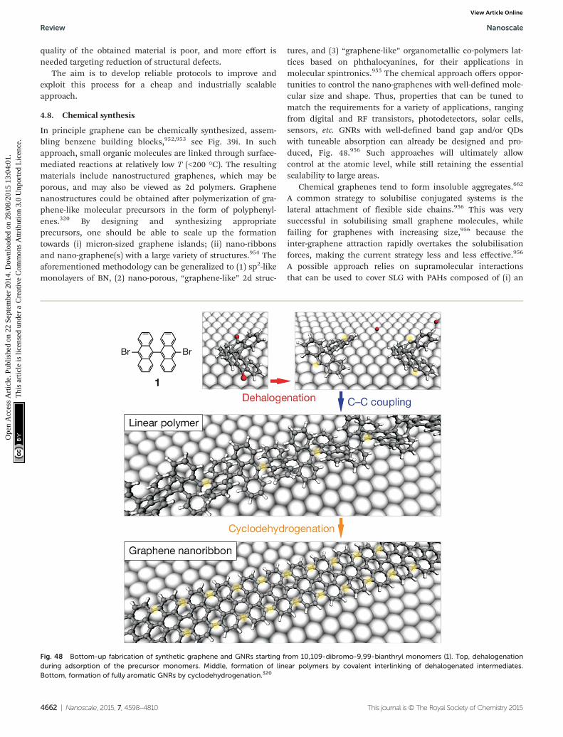
quality of the obtained material is poor, and more effort isneeded targeting reduction of structural defects.
The aim is to develop reliable protocols to improve andexploit this process for a cheap and industrially scalableapproach.
4.8. Chemical synthesis
In principle graphene can be chemically synthesized, assem-bling benzene building blocks,952,953 see Fig. 39i. In suchapproach, small organic molecules are linked through surface-mediated reactions at relatively low T (<200 °C). The resultingmaterials include nanostructured graphenes, which may beporous, and may also be viewed as 2d polymers. Graphenenanostructures could be obtained after polymerization of gra-phene-like molecular precursors in the form of polyphenyl-enes.320 By designing and synthesizing appropriateprecursors, one should be able to scale up the formationtowards (i) micron-sized graphene islands; (ii) nano-ribbonsand nano-graphene(s) with a large variety of structures.954 Theaforementioned methodology can be generalized to (1) sp2-likemonolayers of BN, (2) nano-porous, “graphene-like” 2d struc-
tures, and (3) “graphene-like” organometallic co-polymers lat-tices based on phthalocyanines, for their applications inmolecular spintronics.955 The chemical approach offers oppor-tunities to control the nano-graphenes with well-defined mole-cular size and shape. Thus, properties that can be tuned tomatch the requirements for a variety of applications, rangingfrom digital and RF transistors, photodetectors, solar cells,sensors, etc. GNRs with well-defined band gap and/or QDswith tuneable absorption can already be designed and pro-duced, Fig. 48.956 Such approaches will ultimately allowcontrol at the atomic level, while still retaining the essentialscalability to large areas.
Chemical graphenes tend to form insoluble aggregates.662
A common strategy to solubilise conjugated systems is thelateral attachment of flexible side chains.956 This was verysuccessful in solubilising small graphene molecules, whilefailing for graphenes with increasing size,956 because theinter-graphene attraction rapidly overtakes the solubilisationforces, making the current strategy less and less effective.956
A possible approach relies on supramolecular interactionsthat can be used to cover SLG with PAHs composed of (i) an
Fig. 48 Bottom-up fabrication of synthetic graphene and GNRs starting from 10,109-dibromo-9,99-bianthryl monomers (1). Top, dehalogenationduring adsorption of the precursor monomers. Middle, formation of linear polymers by covalent interlinking of dehalogenated intermediates.Bottom, formation of fully aromatic GNRs by cyclodehydrogenation.320
Review Nanoscale
4662 | Nanoscale, 2015, 7, 4598–4810 This journal is © The Royal Society of Chemistry 2015
Ope
n A
cces
s A
rtic
le. P
ublis
hed
on 2
2 Se
ptem
ber
2014
. Dow
nloa
ded
on 2
8/08
/201
5 13
:04:
01.
Thi
s ar
ticle
is li
cens
ed u
nder
a C
reat
ive
Com
mon
s A
ttrib
utio
n 3.
0 U
npor
ted
Lic
ence
.View Article Online

aromatic core able to interact strongly with graphene and(ii) flexible side chains to make them soluble in most organicsolvents. NGs adsorb reversibly forming ordered layers,with precise control of orientation and spacing.952,953 Theseinteract with the graphene backbone allowing in principle tocontrol and tune its optoelectronic properties,952 while the NGflexible side-chains makes the graphene-NG compositessoluble.957
Supramolecular interactions have the advantage of keepingintact the sp2 network, without compromising the transportproperties.956 Possible applications include the integration ofgraphene with other chemical functionalities, such as metalcontaining dye molecules or reactive sites for the attachmentof biological molecules.
Chemical synthesis is also suited for the formation ofsuperstructures, whose physics is very rich. E.g., the rotationangle between graphene layers controls the carrier velocity.958
There is much more to do in terms of designing and tuningthe strength and type of interaction with the substrate. Noneof the superstructure-induced effects have been thus far har-nessed in real devices. Several directions as starting points forthe realization of such structures and effects can be planned.E.g., the induced growth across atomic islands of insulatingmaterials deposited by nano-stencilling in regular patterns oncatalytic, atomically flat metallic surfaces. Alternatively, explor-ing routes (e.g. thermally, electric field controlled or throughelectronic excitations) for the initiation of cascade chemicalreactions and assembly from NG precursors on insulatingmonolayers and nanostructures to form graphene origami959
and GNRs. Such assembly has only been demonstrated so faron atomically flat metallic surfaces, but molecular self-assem-bly processes show considerable promise and versatility. Novel,volatile, metallo-organic and organometallic complexes couldbe used as the precursors for this process which will provide aroute at the molecular level.
The aim is to explore synthetic graphenes starting fromthe compatibility with a very large range of substrates and theeasy association of organic and inorganic layers. The target isto control with atomic precision the shapes and edges, inorder to tune continuously the band gaps and conductivity,as well as control doping, obtaining a spatial distribution ofdopants with ultimate resolution. Indeed, as the device size ispushed down, the dopant distribution needs to be preciselytuned, which is very difficult to achieve by post-treatment oflarge area graphene, such as hydrogenation or fluorination(or even doping during thin film growth). Precise and tailoreddopant distribution may be assured by means of a hetero-(dopant) atom that is readily part of the precursor molecule.The effect of local doping needs to be investigated. Thiscould be in principle achieved functionalising grapheneusing acceptor/donor molecules that would self-assembleprecisely on its surface. Another challenges for directchemical growth include growth on insulating substrates forelectronic applications and development for efficient transfermethods that allow the nanoribbons to be incorporated inelectronics.
4.9. Nano-ribbons and quantum dots
Ref. 296, 330 prepared GNRs by combining e-beam lithographyand oxygen plasma etching. GNR down to ∼20 nm werereported, with band gap ∼30 meV, then used in FETs with ION/IOFF up to 103 at low T (<5 K) and ∼10 at RT. Ref. 329 reportedmuch smaller GNRs, with minimum width ∼1 nm and gap∼500 meV produced by e-beam lithography and repeated overetching. Sub-10 nm GNRs with bandgap up to 400 meV wereproduced via a chemical route,97 consisting in the dispersionof expanded graphite in liquid phase followed by sonication.Used as channels in FETs, they achieved ION/IOFF up to 107 atRT.303 A solution-based oxidative process was also reported,304
producing GNRs by lengthwise cutting and unravellingSWNTs and MWNTs.332 As result of the oxidative process, suchGNRs show poor conductivity (∼35 S cm−1) and low μ
(0.5–3 cm2 V−1 s−1) at RT.960
Patterning of SLG into sub-10 nm GNRs with predeter-mined crystallographic orientation was achieved by STM litho-graphy,307 by applying a bias higher than for imaging betweenthe STM tip and substrate, while moving the tip at constantvelocity.
GNRs can also be formed without cutting. Ref. 961 demon-strated that spatial selective hydrogenation can be used tocreate graphene “nanorods”, i.e. conductive paths of graphenesurrounded by fully hydrogenated areas. Ref. 962 fabricatedencapsulated ∼35 nm GNRs by depositing a polymer mask viascanning probe lithography, followed by chemical isolation ofthe underlying GNR by fluorinating the uncovered graphene.These GNRs retained μ of non-patterned graphene. Also, thefluorination is reversible, enabling write-erase-rewrite. GNRsdown to 12 nm were produced by local thermal reduction ofGO by scanning probe.963
Sub-10 nm GNRs were fabricated via catalytic hydrogenation,using thermally activated Ni nanoparticles as “knife”.310,964
This allows cutting along specific crystallographic directions,therefore the production of GNRs with well-defined edges.
GNRs were also made via LPE of GICs328 and expandedgraphite.303 Growth on controlled facets on SiC resulted in40 nm GNRs100 and the integration of 10 000 top-gated deviceson a single SiC chip.783
Chemical synthesis seems to be the most promising routetowards well-defined GNRs,678 see Fig. 48. Atomically preciseGNRs were produced by surface assisted coupling of molecularprecursors into linear polyphenylenes and subsequent cyclo-dehydrogenation.678 GNRs up to 40 nm in length and solublein organic solvents such as toluene, dichloromethane andtetrahydrofuran were synthesized336 from polyphenylene pre-cursors having a non-rigid kinked backbone to introducehigher solubility in comparison to that of strictly linear poly(para-phenylene).965
Another route to GNRs is the so-called nanowire litho-graphy,966 consisting in the use of nanowires as masks foranisotropic dry etching. GNRs smaller than the wire itself canbe fabricated via multiple etching.966 Also, the wire, consistingof a crystalline core surrounded by a SiO2 shell, can be used asself-aligned gate.967
Nanoscale Review
This journal is © The Royal Society of Chemistry 2015 Nanoscale, 2015, 7, 4598–4810 | 4663
Ope
n A
cces
s A
rtic
le. P
ublis
hed
on 2
2 Se
ptem
ber
2014
. Dow
nloa
ded
on 2
8/08
/201
5 13
:04:
01.
Thi
s ar
ticle
is li
cens
ed u
nder
a C
reat
ive
Com
mon
s A
ttrib
utio
n 3.
0 U
npor
ted
Lic
ence
.View Article Online
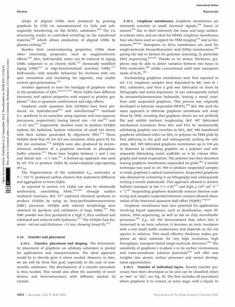
Arrays of aligned GNRs were produced by growinggraphene by CVD on nanostructured Cu foils and sub-sequently transferring on flat Si/SiO2 substrates.968 The Custructuring results in controlled wrinkling on the transferredmaterial,968 which allows production of aligned GNRs byplasma etching.968
Besides their semiconducting properties, GNRs showother interesting properties, such as magnetoelectriceffects.969 Also, half-metallic states can be induced in zigzagGNRs subjected to an electric field,325 chemically modifiedzigzag GNRs970 or edge-functionalized armchair GNRs.971
Half-metals, with metallic behaviour for electrons with onespin orientation and insulating for opposite, may enablecurrent spin-polarization.325
Another approach to tune the bandgap of graphene reliesin the production of QDs.956,972–977 These GQDs have differentelectronic and optical properties with respect to pristine gra-phene1,5 due to quantum confinement and edge effects.
Graphene oxide quantum dots (GOQDs) have been pro-duced via hydrothermal972 and solvothermal973 methods(i.e. synthesis in an autoclave using aqueous and non-aqueousprecursors, respectively) having lateral size ∼10 nm972 and∼5–25 nm,973 respectively. Another route to produce GOQDsexploits the hydrazine hydrate reduction of small GO sheetswith their surface passivated by oligomeric PEG.974 TheseGOQDs show blue PL for 365 nm excitation, while green PL for980 nm excitation.974 GOQDs were also produced by electro-chemical oxidation of a graphene electrode in phosphatebuffer solution.975 These have heights between 1 and 2 nmand lateral size ∼3–5 nm.975 A bottom-up approach was usedby ref. 976 to produce GQDs by metal-catalysed cage-openingof C60.
The fragmentation of the embedded C60 molecules atT ∼ 550 °C produced carbon clusters that underwent diffusionand aggregation to form GQDs.
As reported in section 4.9, GQDs can also be chemicallysynthesized, assembling PAHs,952,956 through surfacemediated reactions. Ref. 977 exploited chemical synthesis toproduce GOQDs by using an hexa-perihexabenzocoronene(HBC) precursor. GOQDs with ordered morphology wereobtained by pyrolysis and exfoliation of large PAHs.977 TheHBC powder was first pyrolyzed at a high T, then oxidized andexfoliated and reduced with hydrazine.977 The GOQDs had dia-meter ∼60 nm and thickness ∼23 nm, showing broad PL.977
4.10. Transfer and placement
4.10.1. Transfer, placement and shaping. The determinis-tic placement of graphene on arbitrary substrates is pivotalfor applications and characterization. The ideal approachwould be to directly grow it where needed. However, to date,we are still far from this goal, especially in the case of non-metallic substrates. The development of a transfer procedureis thus needed. This would also allow the assembly of noveldevices and heterostructures, with different stacked 2dcrystals.
4.10.2. Graphene membranes. Graphene membranes areextremely sensitive to small electrical signals,329 forces ormasses978 due to their extremely low mass and large surface-to-volume ratio, and are ideal for NEMS. Graphene membraneshave also been used as support for TEM imaging979 and as bio-sensors,980,981 Nanopores in SLGs membranes are used forsingle-molecule Deoxyribonucleic acid (DNA) translocation,980
paving the way to devices for genomic screening, in particularDNA sequencing,982,983 Thanks to its atomic thickness, gra-phene may be able to detect variation between two bases inDNA molecules,980 unlike conventional solid state nanoporesmade of Si3N4.
984
Freestanding graphene membranes were first reported inref. 134. Graphene samples were deposited by MC onto Si +SiO2 substrates, and then a grid was fabricated on them bylithography and metal deposition. Si was subsequently etchedby tetramethylammonium hydroxide, leaving a metal canti-lever with suspended graphene. This process was originallydeveloped to fabricate suspended SWNTs.985 Ref. 986 used thesame approach to fabricate graphene membrane and studythem by TEM, revealing that graphene sheets are not perfectlyflat and exhibit intrinsic roughening. Ref. 987 fabricatedmechanical resonators from SLG and FLG by mechanicallyexfoliating graphite over trenches in SiO2. Ref. 988 transferredgraphene exfoliated either on SiO2 or polymer on TEM grids byfirst adhering to the grid and subsequently etching the sub-strate. Ref. 989 fabricated graphene membranes up to 100 μmin diameter by exfoliating graphite on a polymer and sub-sequently fabricating metal scaffolds on it by e-beam litho-graphy and metal evaporation. The polymer was then dissolvedleaving graphene membranes suspended on grids.989 A similartechnique was used in ref. 990 to produce suspended samplesto study graphene’s optical transmission. Suspended graphenewas obtained by contacting it via lithography and subsequentlyetching a trench underneath. This approach allowed to achieveballistic transport at low T (∼4 K)145 and high μ (106 cm2 V−1
s−1).607 Suspending graphene drastically reduces electron scat-tering and samples suspended between contacts allowed obser-vation of the fractional quantum Hall effect (FQHE).144,151
Graphene membranes have also potential for applicationsinvolving liquid separations, such as desalination, water fil-tration, DNA sequencing, as well as lab on chip microfluidicprocesses.991 E.g., ref. 991 demonstrated that, when SLG isimmersed in an ionic solution, it becomes an ionic insulatorswith a very small stable conductance that depends on the ionspecies in solution. This small effective thickness makes gra-phene an ideal substrate for very high resolution, highthroughput, nanopore-based single-molecule detectors.991 Thesensitivity of graphene’s in-plane σ to its surface environmentand trans-membrane solution potentials991 will offer newinsights into atomic surface processes and sensor develop-ment opportunities.
4.10.3. Transfer of individual layers. Several transfer pro-cesses have been developed so far and can be classified eitheras “wet” or “dry”, see Fig. 49. The first includes all procedureswhere graphene is in contact, at some stage, with a liquid. In
Review Nanoscale
4664 | Nanoscale, 2015, 7, 4598–4810 This journal is © The Royal Society of Chemistry 2015
Ope
n A
cces
s A
rtic
le. P
ublis
hed
on 2
2 Se
ptem
ber
2014
. Dow
nloa
ded
on 2
8/08
/201
5 13
:04:
01.
Thi
s ar
ticle
is li
cens
ed u
nder
a C
reat
ive
Com
mon
s A
ttrib
utio
n 3.
0 U
npor
ted
Lic
ence
.View Article Online
the second, one face of graphene is protected from contactingany liquid, while the other is typically in contact with apolymer, eventually dissolved by solvents.
4.10.4. Wet transfer of exfoliated flakes. In 2004 ref. 992placed SWNTs onto arbitrary substrates by transfer printingusing poly(dimethysiloxane) (PDMS) stamps. Ref. 993 reportedtransfer of various nanostructures (such as SWNTs, ZnO nano-wires, gold nanosheets and polystyrene nanospheres) by apoly(methyl methacrylate) (PMMA)-mediated process. In 2008ref. 994 adapted this process to transfer MC graphene onvarious target substrates. The process is based on a PMMAsacrificial layer spin-coated on graphene. The polymer-coatedsample is then immersed in a NaOH solution, which partiallyetches the SiO2 releasing the polymer. Graphene sticks to thepolymer, and can be transferred. PMMA is then dissolved byacetone, releasing graphene.
Ref. 995 reported the deterministic placement of grapheneby exploiting a thin layer of water between the PMMA/graphenefoil and the substrate. Ref. 996 reported transfer of nano-structures (including graphene) embedded in a hydrophobicpolymer. Also in this case, intercalation of water at thepolymer–substrate interface was used to detach the polymer/nanostructures film, then moved on a target substrate.402
PMMA is a positive resist widely used for high resolutione-beam lithography.403 By patterning PMMA, it is also possibleto remove unwanted graphitic material surrounding MC-SLGs,while shaping and isolating the flakes of interest.
4.10.5. Dry transfer of exfoliated flakes. In order to fabri-cate heterostructures with clean interfaces (i.e. withouttrapped adsorbates), dry transfer methods have been develo-ped. Ref. 908 reported a mechanical transfer based on stackingtwo polymer layers, the bottom being water dissolvable andthe top being PMMA. Graphene was exfoliated onto thispolymer stack and the sample floated on the surface of de-ionized (DI) water, resulting in the detachment of the PMMA +graphene film from the substrate. The upper graphene facewas not in contact with water, thus minimizing contami-nation. The polymer + graphene film was then collected andthe alignment achieved using a micromanipulator. Ref. 99used a similar technique to encapsulate graphene between twoh-BN layers, while ref. 997 reported an alternative techniquebased on a glass/tape/copolymer stack. However, ref. 998reported that even dry transfer may not result in perfectlyclean interfaces, as some adsorbates may get trapped.
The Van der Waals interaction between 2d materials wasused to assemble heterostructures such as BN-SLG-BN.999
Fig. 50 shows a schematic of the process where an isolated fewlayer BN flake is used as a stamp to successively pick up alter-nating layers of monolayer graphene and few-layer BN.999 Anadvantage of this technique compared with other transfermethods is that the active interfaces do not contact anypolymer throughout the process, reducing impurities trappedbetween the layers.999
A big challenge is the development of a dry transfer tech-nology for ultrahigh quality graphene up to 450 mm, avoidingthe wet conditions with polymer coating, which suffer frompolymer contamination. The development of dry processes forlarge area graphene on insulator would be extremely useful forlong-term sustainability in device engineering.
Fig. 49 Wet (left) and dry (right) transfer of graphene. Wet transfer: (a)A graphene sample is deposited on oxidized Si by MC. (b) A PMMA film isdeposited by spin coating (c) the PMMA film is detached from the sub-strate either via NaOH etching or water intercalation. Graphene adheresto the polymer and is removed from the Si + SiO2 substrate (d) PMMA +graphene film is “fished” using the target substrate. By sliding the PMMA+ graphene film with respect to the substrate a flake of choice can bealigned with features such as electrodes, cavities, etc. (e) Once thesample has dried, PMMA is dissolved by acetone releasing the grapheneon the target substrate (f ). (g) A graphene flake deposited onto BN bywet transfer. Dry transfer: (h) graphene is exfoliated onto substratescovered by a polymer stack consisting of a water-dissoluble polymer(such as PVA) at the bottom and PMMA on the top. (i) The sample is leftto float in a water bath in such a way that the “release” layer is dissolvedfrom the side. ( j) Graphene is on top of the stack and is never in touchwith water (k) the polymer + graphene film is attached to a specialholder and flipped over. (l) By means of a manipulator the flake ofchoice is placed in the desired position on top of the desired substrate,then the film is pressed on the target substrate (m) PMMA is dissolvedleaving graphene in the desired position (n) graphene layer depositedonto a BN flake by dry transfer. Adapted from ref. 602.
Nanoscale Review
This journal is © The Royal Society of Chemistry 2015 Nanoscale, 2015, 7, 4598–4810 | 4665
Ope
n A
cces
s A
rtic
le. P
ublis
hed
on 2
2 Se
ptem
ber
2014
. Dow
nloa
ded
on 2
8/08
/201
5 13
:04:
01.
Thi
s ar
ticle
is li
cens
ed u
nder
a C
reat
ive
Com
mon
s A
ttrib
utio
n 3.
0 U
npor
ted
Lic
ence
.View Article Online

Optical trapping can also be exploited to manipulate (trans-late, rotate) and deposit trapped graphene250,669 and 2d crys-tals on solid substrates in a controlled fashion.
Optical binding, the formation of extended periodic self-organized (optically bound) structures, could be used for pat-terning and controlled deposition on a substrate over anextended area for parallel nano-lithography. Another promis-ing application of radiation forces is optical stamping litho-graphy,1000 where the repulsive force exerted by a laser beam isexploited to deposit flakes at desired positions on a substrate.Exploiting this, graphene flakes could be optically stamped onsubstrate using holographic patterns (with a Spatial LightModulator), and combined with any other nanomaterial.669
This paves the way for microfluidic integration, expanding theapplicability for biosensing.
4.10.6. Transfer of graphene grown on metals. In 2009,ref. 824 first reported the transfer of SLG and FLG grown byprecipitation on Ni, by depositing a PMMA sacrificial layer andsubsequently etching the underlying Ni by an aqueous HClsolution. Ref. 865 transferred films grown by CVD on Cu,etched by iron nitrite. Ref. 865 introduced etching by aqueousFeCl3 to remove Ni without hydrogen bubbles, which maydamage graphene. It also reported a technique where PDMSstamps are attached directly to the graphene surface. Ni isthen chemically etched by FeCl3 leaving graphene attached tothe PDMS. Graphene is then transferred to SiO2 by pressingand peeling the PDMS. Ref. 7 introduced R2R transfer of gra-phene grown by CVD on Cu foils as large as 30 × 30 in2: athermal release tape was attached to the Cu + graphene foil,and then an etchant removed Cu. The tape + graphene filmwas then attached to a (flexible) target substrate (e.g. PET) andthe supporting tape removed by heating, thus releasing gra-phene onto the target substrate.
To avoid Fe contamination caused by FeCl3 etching,ammonium persulfate [(NH4)2S2O8] was used.1001 To avoidmechanically defects caused by R2R transfer, a hot pressingprocess was developed:1002 similar to a R2R process, the Cu +graphene foil is first attached to thermal release tape and thenCu is chemically etched. The tape + graphene foil is thenplaced on the target substrate and they are inserted betweentwo hot metal plates with controlled temperature and pressure.This results in the detachment of the adhesive tape with very
low frictional stress, therefore less defects, than a R2Rprocess.1002
4.10.7. Di-electrophoresis. Electrophoresis is a techniqueused for separating particles according to their size and electri-cal charge.1003 An uniform electric current is passed through amedium that contains the particles.1003 Particles travelthrough a medium at a different rate, depending on their elec-trical charge and size. Separation occurs based on these differ-ences.1003 Di-electrophoresis (DEP) is the migration ofuncharged particles towards the position of maximum fieldstrength in a non-uniform electric field.1004 The force in DEPdepends on the electrical properties of the particle and sur-rounding fluid, the particle geometry, and electric field fre-quency.1003 Particles move toward the regions of high electricfield strength (positive DEP) if their polarizability is greaterthan the suspending medium,1003 whereas they move in theopposite direction (negative DEP) if the polarizability is lessthan that the suspending medium.1003 This allows fields of aparticular frequency to manipulate particles,1003 at the sametime assembling them on pre-defined locations.1003
In 2003 ref. 1005 reported large area deposition of SWNTsbetween electrode pairs by DEP.410 Subsequently, DEP wasused for the separation of metallic (m-SWNTs) and semi-conducting single wall nanotubes (s-SWNTs),1006 exploitingtheir dielectric constants difference, resulting in oppositemovement of m and s-SWNTs.1006 These SWNT processes werethen adapted for graphene. Ref. 1007, 1008 used DEP for themanipulation of GO soot, and single and few-layer GO flakes.In 2009 ref. 1009 placed individual FLGs between pre-patternedelectrodes via DEP. Once trapped, the higher polarizability ofgraphene compared to the surrounding medium1009 limits thedeposition to one flake per device.1009,1010 Self-limiting is oneof the advantages of this method, together with the directassembly of individual flakes at predetermined locations.
4.10.8. Applications and processing of graphene inks. Dis-persions or inks can be used in a variety of placementmethods, including vacuum filtration, spin and spray coating,ink-jet printing and various R2R processes. The latter are mostattractive because of their manufacturing characteristics, withtransfer speeds in excess of 5 m s−1 currently used in a varietyof applications.1011 R2R consists in processing and printing arapidly moving substrate.1011,1012 Generally, a flexible substrate
Fig. 50 Layer by layer assembly process. (a) Schematic diagram showing the steps to make a BN-SLG-BN stack or a multiple-layer stack with devicelayer (graphene) never exposed to any polymer or solvent. (b) Optical images showing in sequence a BN flake on poly-propylene carbonate (PPC)and film picking. Adapted from ref. 999.
Review Nanoscale
4666 | Nanoscale, 2015, 7, 4598–4810 This journal is © The Royal Society of Chemistry 2015
Ope
n A
cces
s A
rtic
le. P
ublis
hed
on 2
2 Se
ptem
ber
2014
. Dow
nloa
ded
on 2
8/08
/201
5 13
:04:
01.
Thi
s ar
ticle
is li
cens
ed u
nder
a C
reat
ive
Com
mon
s A
ttrib
utio
n 3.
0 U
npor
ted
Lic
ence
.View Article Online
(e.g. paper, textile, polymer) is unrolled from a source roller,coated (i.e. without patterning) or printed (i.e. with pattern-ing), with one or more evaporated materials (e.g. dielectrics) orliquid inks (e.g. inks containing polymers or nanoparticles),simultaneously or in sequence, and treated/cured while thesubstrate continuously moves along the coating/printing roller,before being rolled up again, or cut into individual pieces/devices. Unlike assembly style “pick and place” strategies, thecontinuous fabrication process makes R2R a cheap technol-ogy,1012 ideal for high throughput coating, printing and packa-ging. R2R is a focus of research in plastic electronics, becauseof its high throughout, and low cost compared to otherapproaches (e.g. conventional vacuum deposition and litho-graphy) with similar resolution.1013,1014 A standard R2Rprocess may include evaporation, plasma etching, spray or rod-coating, gravure, flexographic, screen or inkjet printing andlaser patterning.1011 In many R2R processes, e.g., rod-coatingor flexographic printing, solution processing of the ink ormaterial (e.g. polymer, nanoparticles) is required, especiallywhen they cannot1012 be evaporated at low T.1011,1012,1015
Rod-coating employs a wire-wound bar, also known asMayer bar (invented by Charles W. Mayer, who also foundedthe Mayer Coating Machines Company in 1905 in Rochester,USA).1012 This is a stainless steel rod wound with a tight wirespiral, also made of stainless steel. During coating, this createsa thin (∼tens μms) ink layer on a substrate.1013 Spray coatingforms aerosols of the liquid ink, resulting in uniform thin(∼μm) films on a substrate.1012 Screen printing, on the otherhand, uses a plate or screen containing the pattern to beprinted on the substrate.1012 The screen is then placed ontothe target substrate, while the ink is spread across the screenusing a blade, thus transferring the pattern.1012 Flexo- andgravure1015 printing also use a plate to transfer images ontotarget substrates. Flexo uses a relief plate, usually made of flex-ible polymeric material, where the raised sections are coatedwith ink, then transferred onto the substrate by contact print-ing.1012 Gravure uses an engraved metallic plate, consisting ofdots representing pixels.1012 The physical volume of theengraved dots defines the amount of ink stored in them,1016
thus can be used to create gray-scale patterns/images.1016 Ingeneral, different viscosities are preferred for different R2Rtechniques, ranging from 1 to 10 000 mPa s or above,1012,1016.Rod- or spray-coating form uniform films, that may be usedfor larger scale devices (>several cm), the fabrication of TCs,or devices such as batteries or supercapacitors. Screen(∼50–100 μm resolution1012), flexographic (∼40 μm resolu-tion1012) and gravure (∼15 μm resolution1012) printing can beused to print different materials with specific patterns for flex-ible electronics.1016 For resolutions down to ∼50 μm, inkjetprinting offers a mask-less, inexpensive and scalable low-Tprocess.1017 The resolution can be significantly enhanced(<500 nm) by pre-patterning,1017 so that the functionalized pat-terns can act as barriers for the deposited droplets.1017 Thevolume can be reduced to atto-liters/drop by pyroelectrody-namic printing.1018 The process is based on the control oflocal pyroelectric forces, activated by scanning a hot tip or a
laser beam over a functionalized substrate (e.g. lithiumniobate1018), which draw liquid droplets from the reservoir anddeposit them on the underside of the substrate.1018
All of the above techniques can be applied to grapheneinks/dispersions. Large scale placement of LPE graphenecan be achieved via vacuum filtration,35 spin706 and dipcoating,1788 Langmuir–Blodgett662 and spray coating.622
Amongst the R2R techniques, rod-coating has been demon-strated to fabricate TCs.995 Inkjet printing of pristine graphenedispersions was also demonstrated.63 Inkjet printing1019
permits selective deposition and high concentration for par-tially soluble compounds.1020 Ref. 629 reported an inkjetprinted graphene TFTs with μ up to ∼90 cm2 V−1 s−1 and Tr ∼80%. Inkjet printing of GO was also demonstrated,1021–1024 Tominimize clustering of the graphene flakes at the nozzle edge,the flakes should be smaller than 1/50 of the nozzlediameter.629
Inkjet-printing was demonstrated a viable technique toobtain high conductivity graphene patterns.1025 The ink wasprepared exploiting ethanol as solvent and ethyl cellulose asstabilizer.1025 The inkjet-printed graphene features had lowresistivity of 4 mΩ cm, with uniform morphology, compatibil-ity with flexible substrates, and tolerance to bending stresses.
4.11. Contamination and cleaning
Cleaning is a critical part of semiconductor device proces-sing.1026 It is usually performed after patterning and etchingprocesses leave residues.1026 Wet chemical etches are also per-formed to remove damage from surfaces.1026 Most applicationsrequire graphene on a dielectric surface. When graphene isgrown directly on a dielectric as in the case of graphene on SiC[see section 4.2] or when graphene or GO is deposited on thedielectric substrate directly [see section 4.12.3], cleaning isrequired only after patterning and etch processes, as devicesare fabricated. Because every atom is a surface atom, grapheneis very sensitive to contaminants left by production, transfer orfabrication processes. In order to remove them, severalmethods have been developed.
4.11.1. Cleaning of graphene produced by MC
The amount of contamination can be assessed optically.1027
Organic contamination arising from the diffusion of tape glueused in MC changes the contrast.1027 TEM and scanningprobe,1028,1029 microscopy (e.g. AFM, STM), Raman185,1030
together with transport measurements1030 are other viabletechniques to detect contaminants on graphene films orflakes. Ref. 1028 cleaned MC samples from resist residuals bythermal annealing (at 400 °C, in Ar/H2), assessing the qualityof the cleaning process via scanning probe techniques. Ref.1029 introduced thermal annealing (at 280 °C) in ultra-highvacuum (<1.5 × 10⁻¹⁰ Torr), to remove resist residues and othercontaminants. Ref. 1028 cleaned graphene by using highcurrent (∼108 A cm−2). This allows removal of contaminationin situ, and is particularly useful when graphene devices aremeasured in a cryostat.103 Chemical cleaning by chloroformwas reported in ref. 1030. Mechanical cleaning by scanning
Nanoscale Review
This journal is © The Royal Society of Chemistry 2015 Nanoscale, 2015, 7, 4598–4810 | 4667
Ope
n A
cces
s A
rtic
le. P
ublis
hed
on 2
2 Se
ptem
ber
2014
. Dow
nloa
ded
on 2
8/08
/201
5 13
:04:
01.
Thi
s ar
ticle
is li
cens
ed u
nder
a C
reat
ive
Com
mon
s A
ttrib
utio
n 3.
0 U
npor
ted
Lic
ence
.View Article Online
the graphene surface with an AFM tip in contact mode wasalso reported.1031
4.11.2. Cleaning after transfer. Cleaning is particularlyimportant when transferring flakes, as the processes typicallyinvolves sacrificial layers, to be chemically dissolved. Thermalannealing in H2/Ar is normally used to remove polymerresiduals.99,998,1032
In graphene transfer from metals to dielectric surfaces,organic materials such as PMMA or perylene-3,4,9,10-tetra-carboxylic dianhydride (PTCDA) are typically used as thecarrier material, with subsequent chemical removal, e.g. byacetone.6,865 Ref. 1033, 1034 detected by XPS the presence ofresidue on the surface of graphene grown on Cu and trans-ferred onto SiO2. The C1s spectrum was found broader thanthat of graphite and the original graphene on Cu. The broad-ening was associated with the presence of the residue. Uponannealing in high vacuum (10−9 mbar) at T ∼ 300 °C, the C1swidth decreased to a value close to the original graphene onCu.1033,1034 The use of thermal release tape7 (i.e. a tapeadhesive at RT, but that peels off when heated), instead ofPMMA or PTCDA, is more problematic, since tape residues cancontaminate the sample.7 There is some anecdotal evidencethat the presence of residue has a beneficial effect on thenucleation of ALD dielectrics, such as Al2O3.
1035 However, thisapproach to prepare the graphene surface for ALD is not ideal,since the residues have uncontrolled chemical nature and arenot uniform. Ref. 1036 developed a modified RCA transfermethod combining an effective metal cleaning process withcontrol of the hydrophilicity of the target substrates. RCAstands for Radio Corporation of America, the company thatfirst developed a set of wafer cleaning steps in the semiconduc-tor industry.1026 Ref. 1036 demonstrated that RCA offers abetter control both on contamination and crack formationwith respect to the aforementioned approaches.6,7,865
4.11.3. Removal of solvents/surfactants in LPE graphene.For graphene and GO produced via LPE, the cleaning, removalof solvents and/or surfactants, mainly depends on the targetapplications. For composites (both for mechanical134 andphotonic625,1339,1353 applications) the presence of surfactantsdoes not compromise the mechanical and optical properties,thus their removal is not needed, and is in fact essential toavoid agglomeration.625,703,1339,1353 Different is the situationwhen the applications require high conductivity (>104 S cm−1),i.e. TCFs. In this case, solvents/surfactants compromise theinterflake connections, decreasing the conductivity. The sol-vents and the deposition strategy used for the TCFs productionmostly determine the cleaning procedure. In the case of TCFsproduced by vacuum filtration (e.g. on a cellulose filter mem-brane) of surfactant-assisted aqueous dispersions, the as-deposited graphene or RGO films are first rinsed with water towash out the surfactants624,642 and then transferred to thetarget substrate. The membrane is then usually dissolved inacetone and methanol.1037 For freestanding films, the de-posited flakes are peeled off from the membrane.624 The filmsare then annealed at T > 250 °C in Ar/N2
624 or air.642 The latterprocess could help remove residual surfactant molecules.624,642
However, there is no “fixed” T for solvents/surfactants removal,and the different conditions/requirements are ruled by theboiling/melting points of each solvent/surfactant.
4.12. Inorganic layered compounds
4.12.1. Mechanical cleavage. As with graphene,5 individualinorganic sheets can be removed from their parent crystal byMC5,421,1038 MC can involve a single crystal,603 or a singlegrain,603 in the case of polycrystalline materials.1039 The localscale dynamics of the fracture process is complex603 anddepends on the crystal structure.603 To date the lateral size of2d crystals produced via MC is ∼10 μm in h-BN,1040 limited bythe average crystal size of the starting material.1040 Similar sizeflakes (∼10 μm) were also achieved via MC of MoS2, WS2 andNbSe2.
1041
This allowed the structural characterisation of BN by highresolution TEM1038 and its use as a substrate for high perform-ance graphene devices.908 Similarly, for MoS2 a number ofadvances have been demonstrated including the production ofsensors,1042 transistors5,379,1043 and integrated circuits,1044 themeasurement of the mechanical properties of individualnanosheets409 and the observation of the evolution of thevibrational421 and electronic structure,378 with number ofstacked flakes.
As in the case of MC of graphite, MC of LMs is not indust-rially scalable, and MC-flakes are mostly suited for fundamen-tal studies and proof of principle devices.
4.12.2. Laser ablation. Ref. 1045 used laser pulses toablate MoS2 down to a single-layer. Ref. 1045 generated1L-MoS2 in arbitrary shapes and patterns with feature sizesdown to 200 nm, with electronic and optical properties com-parable to MC-1L-MoS2.
1041 Ref. 1045 reported similar PLemission between MC-1L-MoS2 and laser thinned 1L-MoS2,and μ up to 0.49 cm2 V−1 s−1 and up to 0.85 cm2 V−1 s−1 forlaser thinned and MC-1L-MoS2, respectively.
4.12.3. Liquid phase exfoliation. BN,38,1046–1050
TMDs38,396,1051,1052 as well as ternary carbides andnitrides,1053,1054 can be exfoliated in liquids (solvents oraqueous surfactant solutions) by ultrasonication. The exfo-liated sheets can then be stabilised against re-aggregationeither by interaction with the solvent,38 or through electrostaticrepulsion due to the adsorption of surfactant molecules652,1055
In the case of solvent stabilisation, good solvents are thosewith surface energy matching that of the exfoliated materials.38
This results in the enthalpy of mixing being very small.38,1052
Because these exfoliation methods are based on VdWs inter-actions between the flakes and either the solvent molecules orsurfactant tail group, stabilisation does not result in any sig-nificant perturbation of the flake properties. These dispersionscan easily be formed into films or composites38 and facilitateprocessing for a wide range of applications.
The exfoliation and dispersion of LMs were also carried outby the exploitation of co-solvents where the dispersibility ofLMs can be greatly improved by using a mixture of sol-vents1051,1056 e.g., water–ethanol,1051,1056 water–isopropylalcohol,1056 etc. By adjusting the relative concentration of the
Review Nanoscale
4668 | Nanoscale, 2015, 7, 4598–4810 This journal is © The Royal Society of Chemistry 2015
Ope
n A
cces
s A
rtic
le. P
ublis
hed
on 2
2 Se
ptem
ber
2014
. Dow
nloa
ded
on 2
8/08
/201
5 13
:04:
01.
Thi
s ar
ticle
is li
cens
ed u
nder
a C
reat
ive
Com
mon
s A
ttrib
utio
n 3.
0 U
npor
ted
Lic
ence
.View Article Online
co-solvents it is possible to tune the rheological properties1057
of the mixture “on demand”. However, YM and concentrationof the exfoliation process in such co-solvent mixtures is, up todate,1051,1056 much lower than in NMP629 and water-surfactantdispersions.250 Exploitation of co-solvent mixtures,1051,1056,1057
mostly based on water and alcohols, for the dispersion andexfoliation of LMs has some practical disadvantages.1058 Thesurface tension changes exponentially after the addition ofalcohols to water,1057 thus being very sensitive to solvent evap-oration.1056 The rheological properties of alcohol-based co-sol-vents are very temperature sensitive.1057 This is a problem bothduring processing (the ultrasonication causes a temperatureincrease of the dispersion) and for the shelf-life (i.e. themaximum time for which the inks can be stored withoutalteration of their properties) of the dispersions/inks.
Much work remains to be done: exfoliation techniquesmust be extended to a wider range of materials. Both solvent38
and surfactant-exfoliated396 TMDs tend to exist as multilayerstacks with few individual sheets, thus requiring an improve-ment of the exfoliation. The dispersed concentrations (up totens of grams per litres) and the lateral flake size (up to mm)still need to be increased considerably.
In order to pursue these requirements, the development ofa sorting strategy that may allow to control both lateral dimen-sions and N is necessary for the full exploitation of theiroptical and electronic properties.
Quantitative analysis for monitoring the exfoliation (yieldand quality of the as-produced material) of TMDs and TMOs isbased on a range of techniques such as AFM, TEM, Ramanspectroscopy, etc.2337 N can also be controlled via separation incentrifugal fields or by combination with DGU.602,642
The availability of dispersions opens up a range of appli-cations in composites, thin films and inks that can be printedin a variety of ways, and mixed to create hybrids. Many appli-cations in photonics and optoelectronics, such as TCs, thirdgeneration solar cell electrodes, and optical-grade compositesbenefit from LPE produced and assembled materials.
LPE can also produce ribbons with widths <10 nm,303 allow-ing a further in-plane confinement of the 2d crystals, thus anextra handle to tailor their properties. LPE does not requiretransfer techniques and the resulting material can be de-posited on different substrates (rigid and flexible) followingdifferent strategies, such as dip and drop casting, spin, sprayand rod coating, ink-jet printing, etc. Several LMs (includingBN, MoS2, WS2, MoSe2, MoTe2, TaSe2, NbSe2, NiTe2, andBi2Te3) have been already successfully exfoliated using thissimple, yet efficient, method38 that potentially brings also abenefit in terms of chemical stability, as the layer of liquidmight protect the crystallites from oxidation. Such suspen-sions allow, lastly, easy assembling of the materials intosuperstructures.
4.12.4. Synthesis by thin film techniques. A number ofthin film processes can be brought to bear on the growth of 2dcrystals. These range from PVD (e.g. sputtering), evaporation,vapour phase epitaxy, liquid phase epitaxy, chemical vapourepitaxy, MBE, ALE, and many more, including plasma assisted
processes. The selection of the growth process depends on thematerials properties needed and the application. Each materialhas its own challenges. Other than controlling the thicknessand orientation of the films, the composition and stoichi-ometry is of utmost importance because this has large influ-ence on transport. As a result, great care must be taken incontrolling the point defects concentration. Low growth T(∼300 °C) techniques are usually better suited in controllingthe defects arising from vacancies, since the vapour pressureof the chalcogenide elements decreases exponentially withT.1059 However, low T techniques tend to give higher extendeddefect densities because of the lower atomic mobility.1060
Therefore, the growth technique must be selected to match thedesired target application.
To date, WS2 films have been deposited by magnetron sput-tering from both WS1061 and WS2 targets,1062 sulfurization ofW1063 or WO2 films,1064 ion beam mixing,1065 etc. The pre-ferred production process for tribological applications is mag-netron sputtering,1066 because of its lower T than thermallyactivated deposition methods.1066 This is also well suited forlarge area deposition (∼m2).1067 CVD was used to growh-BN,1068 and is now being developed to grow TMDs.1069 Ifsingle layers of the binary films are desired, then ALD or, moreappropriately, ALE might be a better suited.
4.13. Graphene and other 2d crystal hybrids
Technological progress is determined, to a great extent, bydevelopments in material science. The most surprising break-throughs are attained when a new type of material, or newcombinations of known materials, with different dimensional-ity and functionality, are created. Well-known examples are thetransition from 3d semiconducting structures based on Geand Si to 2d semiconducting heterostructures, nowadays theleading platform for microelectronics. Ultimately, the limitsand boundaries of certain applications are given by the veryproperties of the materials naturally available to us. Thus, theband-gap of Si dictates the voltages used in computers, andthe Young’s modulus of steel determines the size of the con-struction beams. Heterostructures based on 2d crystals willdecouple the performance of particular devices from the pro-perties of naturally available materials. 2d crystals have anumber of exciting properties, often unique and very differentfrom those of their 3d counterparts. However, it is thecombinations of such 2d crystals in 3d stacks that offer vastopportunities in designing the functionalities of such hetero-structures. One can combine conductive, insulating, probablysuperconducting and magnetic 2d crystals in one stack withatomic precision, fine-tuning the performance of the resultingmaterial. Furthermore, the functionality of such stacks is“embedded” in the design of such heterostructures.
Heterostructures have already played a crucial role in tech-nology, giving us semiconductor lasers and high μ FETs.However, thus far the choice of materials has been limited tothose which can be grown (typically by MBE) one on top ofanother, thus limiting the types of structures which can beprepared. Instead, 2d crystals of very different nature can be
Nanoscale Review
This journal is © The Royal Society of Chemistry 2015 Nanoscale, 2015, 7, 4598–4810 | 4669
Ope
n A
cces
s A
rtic
le. P
ublis
hed
on 2
2 Se
ptem
ber
2014
. Dow
nloa
ded
on 2
8/08
/201
5 13
:04:
01.
Thi
s ar
ticle
is li
cens
ed u
nder
a C
reat
ive
Com
mon
s A
ttrib
utio
n 3.
0 U
npor
ted
Lic
ence
.View Article Online

combined in one stack with atomic precision, offeringunprecedented control on the properties and functionalities ofthe resulting 2d-based heterostructures. 2d crystals with verydifferent properties can be combined in one 3d structure, pro-ducing novel, multi-functional materials. Most importantly,the functionality of such heterostructures will not simply begiven by the combined properties of the individual layers.Interactions and transport between the layers allow one to gobeyond simple incremental improvements in performance andcreate a truly “quantum leap” in functionality. By carefullychoosing and arranging the individual components one cantune the parameters, creating materials with tailored pro-perties, or “materials on demand”. Following this novelapproach, part of the functionality is brought to the level ofthe design of the material itself.
Inorganic LMs can be exploited for the realization of hetero-structures with graphene, to modulate/change the electronicproperties, thus creating “materials on demand”: hybrid super-structures, with properties not existing in nature,99,106,1070,1078
tailored for novel applications. E.g., superstructures like thosein Fig. 31 (SLG/BN/MoS2/BN/SLG) can be used for tunneldevices, such as diodes, FETs, and light emitting devices, orfor energy application, such as photovoltaic cells.
To date, 3 methods can be envisaged for the production ofatomically thin heterostructures: (I) growth by CVD;1071 (II)layer by layer stacking via mechanical transfer,99,908,1072 and(III) layer by layer deposition of chemically exfoliated 2d crys-tals. However, as the field develops, other techniques willemerge.
CVD is emerging as a promising approach to grow 2d crys-tals. Growth of h-BN1073 and MoS2
1074 was already demon-strated. Ref. 1073 reported growth of single layer h-BN bythermal decomposition of borazine (B3N3H6) on Ni (111). Ref.1074 demonstrated that the CVD growth of MoS2 is scalableand films of any size can be made because the lateral size ofthe layers is defined by the size of the substrates used. More-over, also the thickness of the MoS2 film can be controlledbeing directly dependent on the thickness of the pre-depositedMo metal on the substrate and the as-grown layers can then betransferred onto arbitrary substrates.1074
The aim is to produce a large range of 2d crystals on largescale and with control on demand of N. Low-T CVD and CMOScompatible substrate will be investigated as well all the trans-fer strategies already developed with graphene.
2d crystals can also be produced as nanoribbons (NRs) withtuneable electrical and magnetic properties. MoS2-NRs weremade via electrochemical/chemical synthesis,1075 while zigzagfew- and single-layered BN-NRs were obtained unzipping mul-tiwall BN nanotubes through plasma etching.1076 The target isto produce, within the next 10 years, NRs with controlled elec-trical and optical properties.
Field effect vertical tunnelling transistors based on gra-phene heterostructures with atomically thin BN acting as atunnel barrier, were reported.489 The device operation relies onthe voltage tunability of the tunnel density of states in gra-phene and of the effective height of the tunnel barrier adjacent
to the graphene electrode.489 Ref. 491 used WS2 as an atomic-ally thin barrier, allowing switching between tunnelling andthermionic transport, with much better transistor character-istics with respect to the MoS2 analogue,489 thus reaching amuch higher ION/IOFF ∼ 106. A “barristor”, i.e. a graphene-Sihybrid three-terminal device that mimics a triode operation,was developed by ref. 492. The electrostatically gated gra-phene/Si interface induces a tunable Schottky barrierthat controls charge transport across a vertically stackedstructure.489,491,492
4.13.1. CVD growth of heterostructures. Chemical vapourdeposition is a method suitable for mass production of hetero-structures, though it requires the largest investment and effortin terms of developing the necessary expertise and machinery.There are several indications that such growth is indeed feas-ible:1077 H-BN has already been shown to be effective as a sub-strate for graphene CVD, see Fig. 51.
4.13.2. Mechanical transfer. Transfer of individual 2d crys-tals into heterostructures has been widely demonstrated99,1078
Graphene – BN heterosystems, e.g., have enabled the obser-vation of several interesting effects, including FQHE,908 ballis-tic transport99 and metal–insulator transition in grapheme.1078
‘Dry’ mechanical transfer offers the possibility of controlling/modifying each individual layer as it is being deposited,including by chemical modification, at any stage of the trans-fer procedure. Also, any atomic layer in the multilayer stackcan be individually contacted, offering unprecedented controlon the properties of the stack (one could produce a materialwith individual contacts to every conducting atomic plane).Furthermore, one can apply local strain to individuallayers, which significantly modifies the band structure ofGRMs.19,1079,1080 Important is the control of the relative orien-tation of the layers, which may affect the electronic propertiesof the stack in certain intervals of the energy spectrum.958
4.13.3. Heterostructures from dispersions and inks. Large-scale placement of LPE samples can be achieved by spincoating, Langmuir–Blodgett, spray and rod coating, dip casting(Fig. 52). Surface modifications by SAMs enable targeted large-scale deposition. High uniformity and well defined structureson flexible substrates can also be obtained. DEP can also beused to control the placement of individual crystals between
Fig. 51 Schematic of Graphene/BN stacked film. (a) The Cu foil iscleaned and prepared as the growth substrate. (b) High-quality andlarge-area graphene film is grown via CVD with n-hexane as a liquidcarbon source at 950 °C. (c) The as-grown graphene is then loaded intoanother furnace for the growth of h-BN film on top. Adapted from ref.1077.
Review Nanoscale
4670 | Nanoscale, 2015, 7, 4598–4810 This journal is © The Royal Society of Chemistry 2015
Ope
n A
cces
s A
rtic
le. P
ublis
hed
on 2
2 Se
ptem
ber
2014
. Dow
nloa
ded
on 2
8/08
/201
5 13
:04:
01.
Thi
s ar
ticle
is li
cens
ed u
nder
a C
reat
ive
Com
mon
s A
ttrib
utio
n 3.
0 U
npor
ted
Lic
ence
.View Article Online
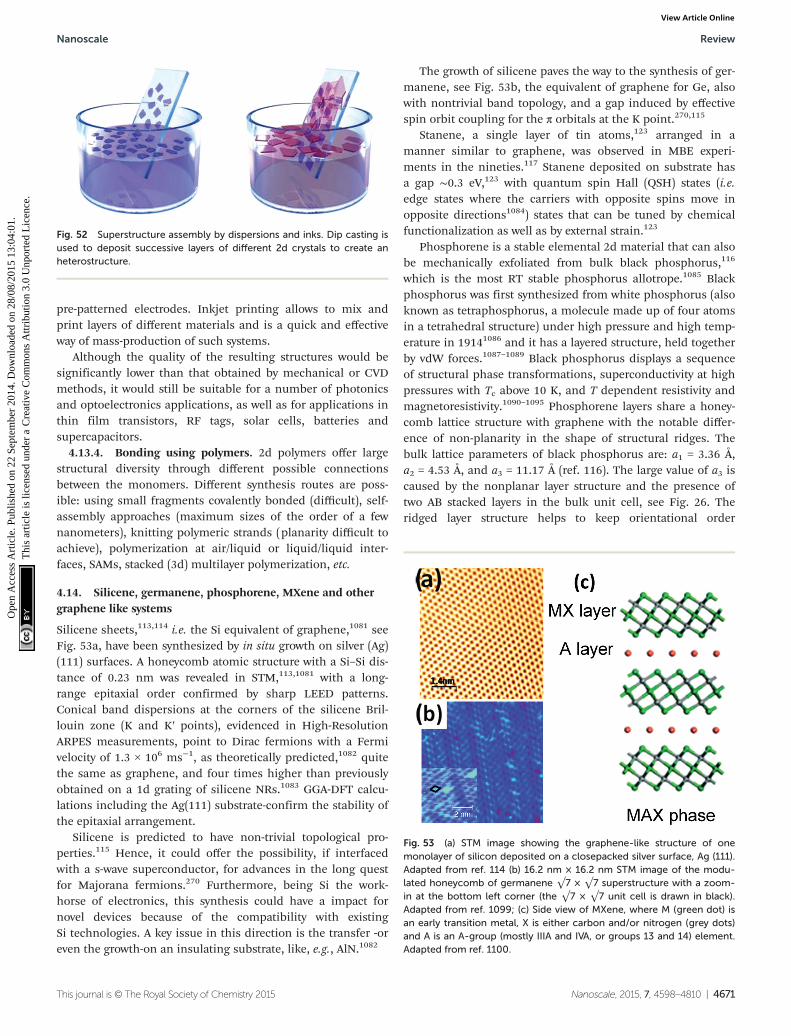
pre-patterned electrodes. Inkjet printing allows to mix andprint layers of different materials and is a quick and effectiveway of mass-production of such systems.
Although the quality of the resulting structures would besignificantly lower than that obtained by mechanical or CVDmethods, it would still be suitable for a number of photonicsand optoelectronics applications, as well as for applications inthin film transistors, RF tags, solar cells, batteries andsupercapacitors.
4.13.4. Bonding using polymers. 2d polymers offer largestructural diversity through different possible connectionsbetween the monomers. Different synthesis routes are poss-ible: using small fragments covalently bonded (difficult), self-assembly approaches (maximum sizes of the order of a fewnanometers), knitting polymeric strands (planarity difficult toachieve), polymerization at air/liquid or liquid/liquid inter-faces, SAMs, stacked (3d) multilayer polymerization, etc.
4.14. Silicene, germanene, phosphorene, MXene and othergraphene like systems
Silicene sheets,113,114 i.e. the Si equivalent of graphene,1081 seeFig. 53a, have been synthesized by in situ growth on silver (Ag)(111) surfaces. A honeycomb atomic structure with a Si–Si dis-tance of 0.23 nm was revealed in STM,113,1081 with a long-range epitaxial order confirmed by sharp LEED patterns.Conical band dispersions at the corners of the silicene Bril-louin zone (K and K′ points), evidenced in High-ResolutionARPES measurements, point to Dirac fermions with a Fermivelocity of 1.3 × 10⁶ ms−1, as theoretically predicted,1082 quitethe same as graphene, and four times higher than previouslyobtained on a 1d grating of silicene NRs.1083 GGA-DFT calcu-lations including the Ag(111) substrate-confirm the stability ofthe epitaxial arrangement.
Silicene is predicted to have non-trivial topological pro-perties.115 Hence, it could offer the possibility, if interfacedwith a s-wave superconductor, for advances in the long questfor Majorana fermions.270 Furthermore, being Si the work-horse of electronics, this synthesis could have a impact fornovel devices because of the compatibility with existingSi technologies. A key issue in this direction is the transfer -oreven the growth-on an insulating substrate, like, e.g., AlN.1082
The growth of silicene paves the way to the synthesis of ger-manene, see Fig. 53b, the equivalent of graphene for Ge, alsowith nontrivial band topology, and a gap induced by effectivespin orbit coupling for the π orbitals at the K point.270,115
Stanene, a single layer of tin atoms,123 arranged in amanner similar to graphene, was observed in MBE experi-ments in the nineties.117 Stanene deposited on substrate hasa gap ∼0.3 eV,123 with quantum spin Hall (QSH) states (i.e.edge states where the carriers with opposite spins move inopposite directions1084) states that can be tuned by chemicalfunctionalization as well as by external strain.123
Phosphorene is a stable elemental 2d material that can alsobe mechanically exfoliated from bulk black phosphorus,116
which is the most RT stable phosphorus allotrope.1085 Blackphosphorus was first synthesized from white phosphorus (alsoknown as tetraphosphorus, a molecule made up of four atomsin a tetrahedral structure) under high pressure and high temp-erature in 19141086 and it has a layered structure, held togetherby vdW forces.1087–1089 Black phosphorus displays a sequenceof structural phase transformations, superconductivity at highpressures with Tc above 10 K, and T dependent resistivity andmagnetoresistivity.1090–1095 Phosphorene layers share a honey-comb lattice structure with graphene with the notable differ-ence of non-planarity in the shape of structural ridges. Thebulk lattice parameters of black phosphorus are: a1 = 3.36 Å,a2 = 4.53 Å, and a3 = 11.17 Å (ref. 116). The large value of a3 iscaused by the nonplanar layer structure and the presence oftwo AB stacked layers in the bulk unit cell, see Fig. 26. Theridged layer structure helps to keep orientational order
Fig. 53 (a) STM image showing the graphene-like structure of onemonolayer of silicon deposited on a closepacked silver surface, Ag (111).Adapted from ref. 114 (b) 16.2 nm × 16.2 nm STM image of the modu-lated honeycomb of germanene √7 × √7 superstructure with a zoom-in at the bottom left corner (the √7 × √7 unit cell is drawn in black).Adapted from ref. 1099; (c) Side view of MXene, where M (green dot) isan early transition metal, X is either carbon and/or nitrogen (grey dots)and A is an A-group (mostly IIIA and IVA, or groups 13 and 14) element.Adapted from ref. 1100.
Fig. 52 Superstructure assembly by dispersions and inks. Dip casting isused to deposit successive layers of different 2d crystals to create anheterostructure.
Nanoscale Review
This journal is © The Royal Society of Chemistry 2015 Nanoscale, 2015, 7, 4598–4810 | 4671
Ope
n A
cces
s A
rtic
le. P
ublis
hed
on 2
2 Se
ptem
ber
2014
. Dow
nloa
ded
on 2
8/08
/201
5 13
:04:
01.
Thi
s ar
ticle
is li
cens
ed u
nder
a C
reat
ive
Com
mon
s A
ttrib
utio
n 3.
0 U
npor
ted
Lic
ence
.View Article Online
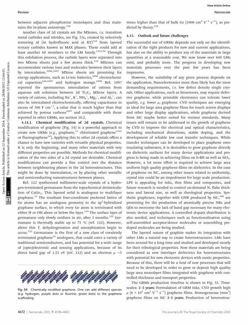
between adjacent phosphorene monolayers and thus main-tains the in-plane anisotropy.116
Another class of 2d crystals are the MXenes, i.e. transitionmetal carbides and nitrides, see Fig. 53c, created by selectivelyremoving Al (in hydrofluoric acid at RT)119 from layeredternary carbides known as MAX phases. These could add atleast another 60 members to the LM family.119,120 Throughthis exfoliation process, the carbide layers were separated intotwo MXene sheets just a few atoms thick.119 MXenes canaccommodate various ions and molecules between their layersby intercalation.1096,1097 MXene sheets are promising forenergy applications, such as Li-ion batteries,1096 electrochemi-cal capacitors120,1097 and hydrogen storage.1098 Ref. 1097reported the spontaneous intercalation of cations fromaqueous salt solutions between 2d Ti3C2 MXene layers. Avariety of cations, including Na+, K+, NH4
+, Mg2+, and Al3
+, canalso be intercalated electrochemically, offering capacitance inexcess of 300 F cm−3, a value that is much higher than thatachieved by porous carbons1097 and comparable with thosereported in other GRMs, see section 10.2.
4.14.1. Chemical modification of 2d crystals. Chemicalmodification of graphene (Fig. 54) is a powerful approach tocreate new GRMs (e.g., graphane,33 chlorinated graphene1101
or fluorographene34). Applying this to other 2d crystals offers achance to have new varieties with versatile physical properties.It is only the beginning, and many other materials with verydifferent properties are possible. Methods for chemical modifi-cation of the two sides of a 2d crystal are desirable. Chemicalmodifications can provide a fine control over the distancebetween neighbouring planes in the 2d heterostructures. Thismight be done by intercalation, or by placing other metallicand semiconducting nanostructures between planes.
Ref. 122 synthesized millimeter-scale crystals of a hydro-gen-terminated germanane from the topochemical deintercala-tion of CaGe2. This layered solid is analogous to multilayergraphane.33 The resultant four-coordinate puckered lattice ofGe atoms has an analogous geometry to the sp3-hybridizedgraphane surface, in which every Ge atom is terminated witheither H or OH above or below the layer.124 The surface layer ofgermanane only slowly oxidizes in air, after 5 months.122 Ger-manane is thermally stable up to 75 °C (ref. 122). However,above this T, dehydrogenation and amorphization begin tooccur.122 Germanane is the first of a new class of covalentlyterminated graphane33 analogues, that could cover a variety oftraditional semiconductors, and has potential for a wide rangeof (opto)electronic and sensing applications, because of itsdirect band gap of 1.53 eV (ref. 122) and an electron μ ∼5
times higher than that of bulk Ge (3900 cm2 V−1 s−1), as pre-dicted by theory.122
4.15. Outlook and future challenges
The successful use of GRMs depends not only on the identifi-cation of the right products for new and current applications,but also on the ability to produce any of the materials in largequantities at a reasonable cost. We now know over 600 LMsexist, and probably more. The progress in developing newmaterials processes over the past few years has beenimpressive.
However, the suitability of any given process depends onthe application. Nanoelectronics more than likely has the mostdemanding requirements, i.e. low defect density single crys-tals. Other applications, such as biosensors, may require defec-tive graphene, while printable electronics can tolerate lowerquality, e.g. lower μ, graphene. CVD techniques are emergingas ideal for large area graphene films for touch screen displaysand other large display applications, while graphene derivedfrom SiC maybe better suited for resistor standards. Manyissues still remain to be addressed in the growth of grapheneby CVD to improve the electrical and optical characteristics,including mechanical distortions, stable doping, and thedevelopment of reliable low cost transfer techniques. Whiletransfer techniques can be developed to place graphene ontoinsulating substrates, it is desirables to grow graphene directlyon dielectric surfaces for many device applications and pro-gress is being made in achieving films on h-BN as well as SiO2.However, a lot more effort is required to achieve large areauniform high quality graphene films on dielectrics. In the caseof graphene on SiC, among other issues related to uniformity,crystal size could be an impediment for large scale production.LPE is appealing for inks, thin films and composites, andfuture research is needed to control on-demand N, flake thick-ness and lateral size, as well as rheological properties. Syn-thetic graphenes, together with GNR produced by SiC,100 arepromising for the production of atomically precise NRs andQDs to overcome the lack of band gap necessary for many elec-tronic device applications. A controlled dopant distribution isalso needed, and techniques such as functionalization usingself-assembled acceptor/donor molecules or assembling pre-doped molecules are being studied.
The layered nature of graphite makes its integration withother LMs a natural way to create heterostructures. LMs havebeen around for a long time and studied and developed mostlyfor their tribological properties. Now these materials are beingconsidered as new interlayer dielectrics for heterostructureswith potential for new electronic devices with exotic properties.Because of this, there will be a host of new processes that willneed to be developed in order to grow or deposit high qualitylarge area monolayer films integrated with graphene with con-trolled thickness and transport properties.
The GRMs production timeline is shown in Fig. 55. Time-scales: 2–3 years: Formulation of GRM inks. CVD growth highμ (6 × 104 cm2 V−1 s−1) graphene films. Homogeneous (mm2)graphene films on SiC 3–5 years: Production of heterostruc-
Fig. 54 Chemically modified graphene. One can add different species(e.g. hydrogen, purple dots or fluorine, green dots) to the graphenescaffolding.
Review Nanoscale
4672 | Nanoscale, 2015, 7, 4598–4810 This journal is © The Royal Society of Chemistry 2015
Ope
n A
cces
s A
rtic
le. P
ublis
hed
on 2
2 Se
ptem
ber
2014
. Dow
nloa
ded
on 2
8/08
/201
5 13
:04:
01.
Thi
s ar
ticle
is li
cens
ed u
nder
a C
reat
ive
Com
mon
s A
ttrib
utio
n 3.
0 U
npor
ted
Lic
ence
.View Article Online
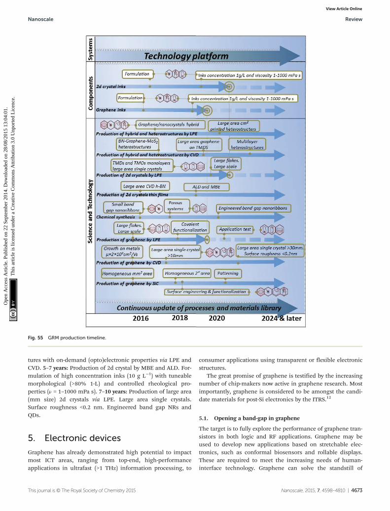
tures with on-demand (opto)electronic properties via LPE andCVD. 5–7 years: Production of 2d crystal by MBE and ALD. For-mulation of high concentration inks (10 g L−1) with tuneablemorphological (>80% 1-L) and controlled rheological pro-perties (ν = 1–1000 mPa s). 7–10 years: Production of large area(mm size) 2d crystals via LPE. Large area single crystals.Surface roughness <0.2 nm. Engineered band gap NRs andQDs.
5. Electronic devices
Graphene has already demonstrated high potential to impactmost ICT areas, ranging from top-end, high-performanceapplications in ultrafast (>1 THz) information processing, to
consumer applications using transparent or flexible electronicstructures.
The great promise of graphene is testified by the increasingnumber of chip-makers now active in graphene research. Mostimportantly, graphene is considered to be amongst the candi-date materials for post-Si electronics by the ITRS.12
5.1. Opening a band-gap in graphene
The target is to fully explore the performance of graphene tran-sistors in both logic and RF applications. Graphene may beused to develop new applications based on stretchable elec-tronics, such as conformal biosensors and rollable displays.These are required to meet the increasing needs of human-interface technology. Graphene can solve the standstill of
Fig. 55 GRM production timeline.
Nanoscale Review
This journal is © The Royal Society of Chemistry 2015 Nanoscale, 2015, 7, 4598–4810 | 4673
Ope
n A
cces
s A
rtic
le. P
ublis
hed
on 2
2 Se
ptem
ber
2014
. Dow
nloa
ded
on 2
8/08
/201
5 13
:04:
01.
Thi
s ar
ticle
is li
cens
ed u
nder
a C
reat
ive
Com
mon
s A
ttrib
utio
n 3.
0 U
npor
ted
Lic
ence
.View Article Online

stretchable electronics, due to the difficulty in developingsemiconducting materials with the high stretchability requiredfor such applications. Fig. 56 and Table 3 show some possibleapplications and an indication of when functional device pro-totypes could be expected.
Graphene can replace materials in several existing appli-cations, but the combination of its unique properties shouldinspire completely new applications, which is the ultimatetarget.
The major obstacle of graphene in transistor applications,especially for ICs as potential Si replacement, is its zero band-gap. This is responsible for the low ION/IOFF in GFETs due to anon-zero off state drain current, which leads to considerablestatic power dissipation. E.g., the typical static drain current ingraphene inverters1102 is ∼270 μA μm−1 at a supply voltage VDD= 2.5 V, in contrast to the much smaller leakage drain current∼100nA μm−1 at VDD = 0.75 V in 22 nm node high-performanceSi logic transistors.1103 Small band gap opening was observedin large area hybrid films, consisting of graphene and h-BNdomains synthesized on Cu substrates by CVD.1104
Thus, opening a band gap without compromising any of itsother outstanding properties, such as high-field transport andμ, is one of the most active research areas. Apart fromquantum confinement (GNRs and GQDs), many other tech-niques have been developed for this goal. Substrate inducedband-gap opening was investigated.1105 Band-gap opening ingraphene, both on h-BN and h-BN/Ni(111) with band gap upto 0.5 eV was reported.1106 Theory suggests that a band gap∼0.52 eV can be opened in graphene deposited on oxygen ter-minated SiO2 surfaces.1107 A bandgap is observed for BLGgrown on SiC.1108
Substitutional doping is another promising route foropening a band gap. Nitrogen doping might be used toconvert graphene into a p-type semiconductor.1109
A few other approaches also exist for band gap engineering.Formation of GNRs with finite band gaps is possible usingconventional BC lithography.339 A band gap ∼0.7 eV wasdemonstrated by selective hydrogenation of graphene on Ir.358
Molecular doping and charge transfer methods could alsomodulate the electronic properties via paramagnetic adsor-bates and impurities that can dope graphene.1110 Selectivechemical functionalization can also be used for band gapengineering.33,34 Complete hydrogenation of graphene formsgraphane, an insulator,33 while a similar process using Fluor-
ine, produces fluorographene.34 The latter is optically trans-parent with a gap ∼3 eV.34 If an electric field is appliedperpendicular to BLG, a gap opens, with size dependent onthe strength of the field.127,1111–1113
The organic synthesis of GNRs seems to be a powerfultool.320 However, as reported in section 4.9, a reliable approachfor on-demand bandgap engineered GNRs needs to be develo-ped. Band-gap opening in graphene on SiC sparked a lot ofinterest because of the viability of the growth process.Recently, STS measurements taken on GNRs grown on theterrace structure of SiC have shown a gap of more than 1 eV(ref. 100). However, graphene grown on SiC tends to be elec-tron doped and the Fermi level lies above the gap. To make it
Table 3 Drivers leading the implementation of graphene for differentelectronic applications and issues to be resolved with current graphenetechnology
Application DriversIssue to beaddressed
Touchscreen
Better endurance with grapheneas compared to other materials
Need to bettercontrol contactresistance
E-paper High Tr of SLG; Visibility Need to bettercontrol contactresistance
FoldableOLED
Graphene with highelectrical properties andbendability
Need to improvethe Rs
Efficiency improved dueto graphene’s workfunction tunability
Need to controlcontact resistance
Atomically flat surface ofgraphene helps to avoidelectrical shorts andleakage current.
Need a conformalcoverage of 3dstructures
RFTransistor
No manufacturable solution forInP high-electron-μ transistors(HEMT) (low noise) after 2021according to the 2011 ITRS
Need to achievecurrent saturationfT = 850 GHz, fmax= 1200 GHz shouldbe achieved
LogicTransistor
High μ New structuresNeed to resolve theband-gap/μ trade-offNeed ION/IOFF >10
6
Fig. 56 GRM electronics’ application timeline. The rectangles in the figure indicate the timeframe when functional device prototypes could be expected.
Review Nanoscale
4674 | Nanoscale, 2015, 7, 4598–4810 This journal is © The Royal Society of Chemistry 2015
Ope
n A
cces
s A
rtic
le. P
ublis
hed
on 2
2 Se
ptem
ber
2014
. Dow
nloa
ded
on 2
8/08
/201
5 13
:04:
01.
Thi
s ar
ticle
is li
cens
ed u
nder
a C
reat
ive
Com
mon
s A
ttrib
utio
n 3.
0 U
npor
ted
Lic
ence
.View Article Online
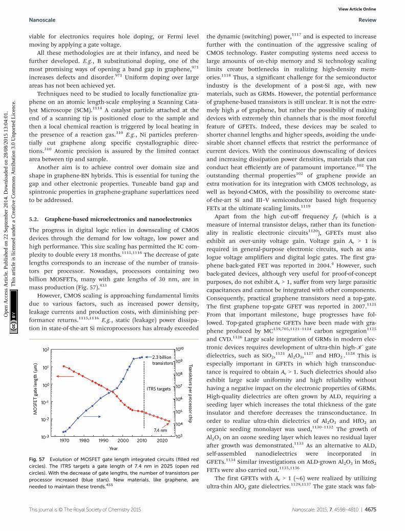
viable for electronics requires hole doping, or Fermi levelmoving by applying a gate voltage.
All these methodologies are at their infancy, and need befurther developed. E.g., B substitutional doping, one of themost promising ways of opening a band gap in graphene,971
increases defects and disorder.971 Uniform doping over largeareas has not been achieved yet.
Techniques need to be studied to locally functionalize gra-phene on an atomic length-scale employing a Scanning Cata-lyst Microscope (SCM).1114 A catalyst particle attached at theend of a scanning tip is positioned close to the sample andthen a local chemical reaction is triggered by local heating inthe presence of a reaction gas.310 E.g., Ni particles preferen-tially cut graphene along specific crystallographic direc-tions.310 Atomic precision is assured by the limited contactarea between tip and sample.
Another aim is to achieve control over domain size andshape in graphene-BN hybrids. This is essential for tuning thegap and other electronic properties. Tuneable band gap andspintronic properties in graphene-graphane superlattices needto be addressed.
5.2. Graphene-based microelectronics and nanoelectronics
The progress in digital logic relies in downscaling of CMOSdevices through the demand for low voltage, low power andhigh performance. This size scaling has permitted the IC com-plexity to double every 18 months.1115,1116 The decrease of gatelengths corresponds to an increase of the number of transis-tors per processor. Nowadays, processors containing twobillion MOSFETs, many with gate lengths of 30 nm, are inmass production (Fig. 57).433
However, CMOS scaling is approaching fundamental limitsdue to various factors, such as increased power density,leakage currents and production costs, with diminishing per-formance returns.1115,1116 E.g., static (leakage) power dissipa-tion in state-of-the-art Si microprocessors has already exceeded
the dynamic (switching) power,1117 and is expected to increasefurther with the continuation of the aggressive scaling ofCMOS technology. Faster computing systems need access tolarge amounts of on-chip memory and Si technology scalinglimits create bottlenecks in realizing high-density mem-ories.1118 Thus, a significant challenge for the semiconductorindustry is the development of a post-Si age, with newmaterials, such as GRMs. However, the potential performanceof graphene-based transistors is still unclear. It is not the extre-mely high μ of graphene, but rather the possibility of makingdevices with extremely thin channels that is the most forcefulfeature of GFETs. Indeed, these devices may be scaled toshorter channel lengths and higher speeds, avoiding the unde-sirable short channel effects that restrict the performance ofcurrent devices. With the continuous downscaling of devicesand increasing dissipation power densities, materials that canconduct heat efficiently are of paramount importance.102 Theoutstanding thermal properties102 of graphene provide anextra motivation for its integration with CMOS technology, aswell as beyond-CMOS, with the possibility to overcome state-of-the-art Si and III–V semiconductor based high frequencyFETs at the ultimate scaling limits.1119
Apart from the high cut-off frequency fT (which is ameasure of internal transistor delays, rather than its function-ality in realistic electronic circuits1120), GFETs must alsoexhibit an over-unity voltage gain. Voltage gain Av > 1 isrequired in general-purpose electronic circuits, such as ana-logue voltage amplifiers and digital logic gates. The first gra-phene back-gated FET was reported in 2004.4 However, suchback-gated devices, although very useful for proof-of-conceptpurposes, do not exhibit Av > 1, suffer from very large parasiticcapacitances and cannot be integrated with other components.Consequently, practical graphene transistors need a top-gate.The first graphene top-gate GFET was reported in 2007.1121
From that important milestone, huge progresses have fol-lowed. Top-gated graphene GFETs have been made with gra-phene produced by MC159,705,1121–1124 carbon segregation1125
and CVD.1126 Large scale integration of GRMs in modern elec-tronic devices requires development of ultra-thin high-K gatedielectrics, such as SiO2,
1121 Al2O3,1127 and HfO2 .
1128 This isespecially important in GFETs in which high transconduc-tance is required to obtain Av > 1. Such dielectrics should alsoexhibit large scale uniformity and high reliability withouthaving a negative impact on the electronic properties of GRMs.High-quality dielectrics are often grown by ALD, requiring aseeding layer which increases the total thickness of the gateinsulator and therefore decreases the transconductance. Inorder to realize ultra-thin dielectrics of Al2O3 and HfO2 anorganic seeding monolayer was used,1130–1132 The growth ofAl2O3 on an ozone seeding layer which leaves no residual layerafter growth was demonstrated.1133 As an alternative to ALD,self-assembled nanodielectrics were incorporated inGFETs.1134 Similar investigations on ALD-grown Al2O3 in MoS2FETs were also carried out.1135,1136
The first GFETs with Av > 1 (∼6) were realized by utilizingultra-thin AlOx gate dielectrics.1129,1137 The gate stack was fab-
Fig. 57 Evolution of MOSFET gate length integrated circuits (filled redcircles). The ITRS targets a gate length of 7.4 nm in 2025 (open redcircles). With the decrease of gate lengths, the number of transistors perprocessor increased (blue stars). New materials, like graphene, areneeded to maintain these trends.433
Nanoscale Review
This journal is © The Royal Society of Chemistry 2015 Nanoscale, 2015, 7, 4598–4810 | 4675
Ope
n A
cces
s A
rtic
le. P
ublis
hed
on 2
2 Se
ptem
ber
2014
. Dow
nloa
ded
on 2
8/08
/201
5 13
:04:
01.
Thi
s ar
ticle
is li
cens
ed u
nder
a C
reat
ive
Com
mon
s A
ttrib
utio
n 3.
0 U
npor
ted
Lic
ence
.View Article Online

ricated by evaporation of Al followed by exposure to air. Thisnaturally forms a very thin (<4 nm) AlOx layer at the interfacebetween graphene and the Al layer evaporated on top.1129,1137
However, these GFETs exhibited Av > 1 only at cryogenicT,1129,1137 as strong hysteresis observed in their transfer charac-teristics suppressed Av at RT.
1137 Hysteretic behaviour of GFETsunder ambient conditions stems from water charge trapsadsorbed on the substrate,1138–1140 which has a detrimentalimpact on their transconductance, therefore on Av. The firstAv > 1 under ambient conditions1141 was obtained by deployingmisoriented BLG as active material and using a solid polymerelectrolyte as gate dielectric.1141 However, these devices exhibi-ted Av > 1 only in direct current (DC) mode, as a consequenceof a large overlap between the polymer gate and source/draincontacts.1141 DC gain is of no interest in realistic electronicapplications, as logic gates and voltage amplifiers operate indynamic, alternating current (AC) mode. An AC Av > 1 wasfirstly demonstrated at RT in a 6-finger-gate GFET configur-ation.1142 The obtained gain was small (Av = 1.7) and thedevices were not integrated (they required external inductorsand capacitors to operate). Despite this, they exhibited promis-ingly large bandwidth (6 GHz).1142
Soon thereafter integrated graphene voltage amplifiers weredemonstrated.1143 They exhibited the highest AC voltage gain(Av = 3.7) reported until then in SLG-FETs at RT.1143 In contrastto standard GFETs in which there are ungated parts of gra-phene channel on either side of the gate, those in ref. 1143 didnot have ungated parts, due to a self-aligned fabricationprocess. This also eliminated hysteresis in the transfer curve,thus far detrimental in obtaining Av > 1 at RT. Such a uniqueblend of transistor properties combined with the use of verythin gate insulators resulted in Av that can readily be utilizedboth in analogue and digital electronics. However, thesedevices were fabricated from MC graphene, unsuitable formass production. The highest Av reported so far in self-alignedtop-gated wafer-scale GFETs under ambient conditions is5.3.1144 Such gain allowed graphene integrated complementaryinverters to exhibit digital signal matching at RT.1144 Cascad-ing of digital inverters in which the previous stage is capableof triggering the next stage, was also demonstrated.1144 Thisapproach resulted in the realization of integrated graphenering oscillators (GROs), consisting of an odd number of inver-ters cascaded in a loop which makes the RO unstable inducingoscillation, operating at GHz frequencies. These GROs are thefastest demonstrated in any low-dimensional nanomaterial todate.1102 The highest Av reported so far in GFETs is 35, but inexfoliated BLG subject to perpendicular electric fields.87
The channels of most top-gated transistors are made oflarge-area graphene, with a minimum conductivity (∼4 e2 h−1),even within the limit of nominally zero carrier concentration.74
This is too high for applications in logic elements, as it leadsto high leakage in the off state and poses serious limitationsfor the switching of these devices. Thus, one option for gra-phene in digital logic relies on bandgap opening. To date, theformation of GNRs seems the most promising route andGFETs with back-gate control were demonstrated.312 Such
devices operate as p-channels with ION/IOFF ∼ 106 (ref. 312).Ref. 1122 reported top-gated GNR GFETs with HfO2 top-gatedielectric, with a RT ION/IOFF ∼ 70. Proof of principle deviceswere demonstrated in BLG GFETs, with ION/IOFF ∼ 2000 at lowT, and 100 at RT.1145 However, large ION/IOFF must be obtainedtogether with Av > 1 for these GFETs to be usable in practicalapplications, i.e., large μ must be preserved while opening theband gap.
The high μ, coupled with high κ and high current density,make graphene ideal as a replacement for Cu inter-connects.1146 Theoretical projections suggest that graphenewith low line-widths (<8 nm) may outperform Cu.1146 Thus,although for digital electronics the entry of graphene isexpected on a longer timescale, Fig. 61, the first components,such as interconnects, may be fabricated within the next fewyears. The long-term target plan (>20 years) is to transform gra-phene transistors, from being excellent tools to probe thetransport properties of this material, to viable devices tocompete and replace/integrate state-of-the-art Si and com-pound semiconductor electronics. Routes for realizing gra-phene-based digital electronics need to be explored andassessed to fully exploit the potential of this material to bringthe semiconductor industry beyond the 7.4 nm node, whichthe ITRS expects to be reached in 2025 (ref. 12).
GFETs with controlled threshold voltage and bothn-channel and p-channel need to be demonstrated for CMOSlogic. The contact resistance between the metallic source anddrain and graphene channel should be investigated deeply andmore focussed research is needed to understand the contactproperties. New graphene device concepts, such as tunnelFETs (TFETs) and bilayer pseudospin FETs (BISFET)1147 needto be studied, and different design options must be explored,evaluated and optimized. The BiSFET is based on the electricalproperties of two layers of graphene in close proximity.1147
Electrons in one layer can pair with holes (both Fermions) inthe opposite layer resulting in e–h-pairs/excitons (Bosons)which then can condense.1147 The condensation alters thequantum wavefunctions in the bilayer structure, convertingstates that were isolated in one of the two layers into statesthat are a coherent linear combination of top and bottom layercomponents.1148 This qualitative change effectively shorts thetwo layers, reducing the tunnel resistance from a large value toa value limited by contacts only.1147 The reduction in tunnelresistance applies only for small interlayer bias, however,because high current destroys the condensate.1148 The BiSFETexploits the I–V nonlinearities associated with this maximumtunnel current, allowing, in principle, lower voltage, lowerpower operation than possible with CMOS FETs.1147
Moreover, the integration with exiting CMOS technology isa critical step in establishing a pathway for grapheneelectronics.
Another crucial point concerns the steady increase in powerdissipation demand per unit area (despite the reduction of thesupply voltage). This is becoming a major issue for the designof next-generation devices: it is mandatory to efficientlyremove heat. Besides its practical importance, the investigation
Review Nanoscale
4676 | Nanoscale, 2015, 7, 4598–4810 This journal is © The Royal Society of Chemistry 2015
Ope
n A
cces
s A
rtic
le. P
ublis
hed
on 2
2 Se
ptem
ber
2014
. Dow
nloa
ded
on 2
8/08
/201
5 13
:04:
01.
Thi
s ar
ticle
is li
cens
ed u
nder
a C
reat
ive
Com
mon
s A
ttrib
utio
n 3.
0 U
npor
ted
Lic
ence
.View Article Online
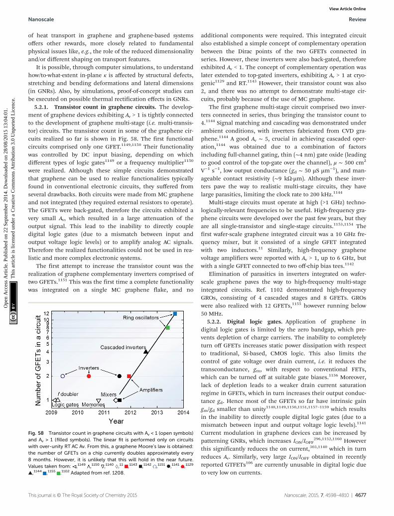
of heat transport in graphene and graphene-based systemsoffers other rewards, more closely related to fundamentalphysical issues like, e.g., the role of the reduced dimensionalityand/or different shaping on transport features.
It is possible, through computer simulations, to understandhow/to-what-extent in-plane κ is affected by structural defects,stretching and bending deformations and lateral dimensions(in GNRs). Also, by simulations, proof-of-concept studies canbe executed on possible thermal rectification effects in GNRs.
5.2.1. Transistor count in graphene circuits. The develop-ment of graphene devices exhibiting Av > 1 is tightly connectedto the development of graphene multi-stage (i.e. multi-transis-tor) circuits. The transistor count in some of the graphene cir-cuits realized so far is shown in Fig. 58. The first functionalcircuits comprised only one GFET.1149,1150 Their functionalitywas controlled by DC input biasing, depending on whichdifferent types of logic gates1149 or a frequency multiplier1150
were realized. Although these simple circuits demonstratedthat graphene can be used to realize functionalities typicallyfound in conventional electronic circuits, they suffered fromseveral drawbacks. Both circuits were made from MC grapheneand not integrated (they required external resistors to operate).The GFETs were back-gated, therefore the circuits exhibited avery small Av, which resulted in a large attenuation of theoutput signal. This lead to the inability to directly coupledigital logic gates (due to a mismatch between input andoutput voltage logic levels) or to amplify analog AC signals.Therefore the realized functionalities could not be used in rea-listic and more complex electronic systems.
The first attempt to increase the transistor count was therealization of graphene complementary inverters comprised oftwo GFETs.1151 This was the first time a complete functionalitywas integrated on a single MC graphene flake, and no
additional components were required. This integrated circuitalso established a simple concept of complementary operationbetween the Dirac points of the two GFETs connected inseries. However, these inverters were also back-gated, thereforeexhibited Av < 1. The concept of complementary operation waslater extended to top-gated inverters, exhibiting Av > 1 at cryo-genic1129 and RT.1143 However, their transistor count was also2, and there was no attempt to demonstrate multi-stage cir-cuits, probably because of the use of MC graphene.
The first graphene multi-stage circuit comprised two inver-ters connected in series, thus bringing the transistor count to4.1144 Signal matching and cascading was demonstrated underambient conditions, with inverters fabricated from CVD gra-phene.1144 A good Av ∼ 5, crucial in achieving cascaded oper-ation,1144 was obtained due to a combination of factorsincluding full-channel gating, thin (∼4 nm) gate oxide (leadingto good control of the top-gate over the channel), μ ∼ 500 cm2
V−1 s−1, low output conductance (gd ∼ 50 µS µm−1), and man-ageable contact resistivity (∼9 kΩ·µm). Although these inver-ters pave the way to realistic multi-stage circuits, they havelarge parasitics, limiting the clock rate to 200 kHz.1144
Multi-stage circuits must operate at high (>1 GHz) techno-logically-relevant frequencies to be useful. High-frequency gra-phene circuits were developed over the past few years, but theyare all single-transistor and single-stage circuits.1153,1154 Thefirst wafer-scale graphene integrated circuit was a 10 GHz fre-quency mixer, but it consisted of a single GFET integratedwith two inductors.11 Similarly, high-frequency graphenevoltage amplifiers were reported with Av > 1, up to 6 GHz, butwith a single GFET connected to two off-chip bias tees.1142
Elimination of parasitics in inverters integrated on wafer-scale graphene paves the way to high-frequency multi-stageintegrated circuits. Ref. 1102 demonstrated high-frequencyGROs, consisting of 4 cascaded stages and 8 GFETs. GROswere also realized with 12 GFETs,1155 however running below50 MHz.
5.2.2. Digital logic gates. Application of graphene indigital logic gates is limited by the zero bandgap, which pre-vents depletion of charge carriers. The inability to completelyturn off GFETs increases static power dissipation with respectto traditional, Si-based, CMOS logic. This also limits thecontrol of gate voltage over drain current, i.e. it reduces thetransconductance, gm, with respect to conventional FETs,which can be turned off at suitable gate biases.1156 Moreover,lack of depletion leads to a weaker drain current saturationregime in GFETs, which in turn increases their output conduc-tance gd. Hence most of the GFETs so far have intrinsic gaingm/gd smaller than unity1140,1149,1150,1151,1157–1159 which resultsin the inability to directly couple digital logic gates (due to amismatch between input and output voltage logic levels).1141
Current modulation in graphene devices can be increased bypatterning GNRs, which increases ION/IOFF
296,1152,1160 Howeverthis significantly reduces the on current,303,1140 which in turnreduces Av. Similarly, very large ION/IOFF obtained in recentlyreported GTFETs106 are currently unusable in digital logic dueto very low on currents.
Fig. 58 Transistor count in graphene circuits with Av < 1 (open symbols)and Av > 1 (filled symbols). The linear fit is performed only on circuitswith over-unity RT AC Av. From this, a graphene Moore’s law is obtained:the number of GFETs on a chip currently doubles approximately every8 months. However, it is unlikely that this will hold in the near future.Values taken from: ,1149 ,1150 ,1140 ◊,11 ,1143 ■,1142 ,1151 ●,1141 ,1129
▲,1144 ,1155 .1102 Adapted from ref. 1208.
Nanoscale Review
This journal is © The Royal Society of Chemistry 2015 Nanoscale, 2015, 7, 4598–4810 | 4677
Ope
n A
cces
s A
rtic
le. P
ublis
hed
on 2
2 Se
ptem
ber
2014
. Dow
nloa
ded
on 2
8/08
/201
5 13
:04:
01.
Thi
s ar
ticle
is li
cens
ed u
nder
a C
reat
ive
Com
mon
s A
ttrib
utio
n 3.
0 U
npor
ted
Lic
ence
.View Article Online
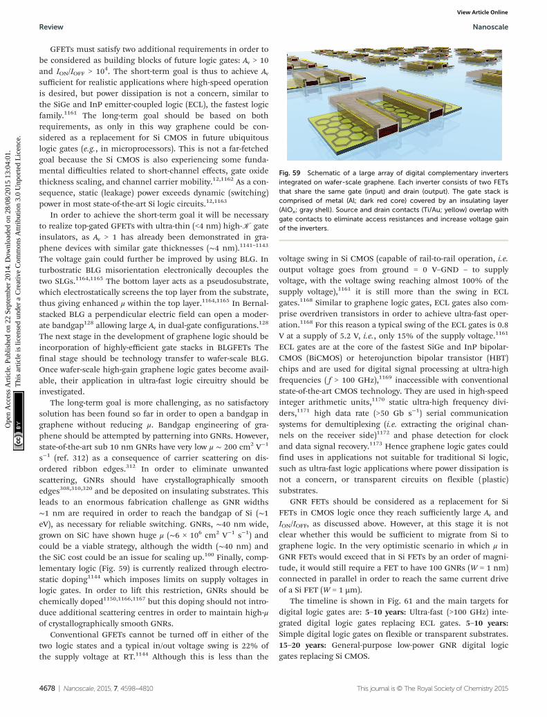
GFETs must satisfy two additional requirements in order tobe considered as building blocks of future logic gates: Av > 10and ION/IOFF > 104. The short-term goal is thus to achieve Avsufficient for realistic applications where high-speed operationis desired, but power dissipation is not a concern, similar tothe SiGe and InP emitter-coupled logic (ECL), the fastest logicfamily.1161 The long-term goal should be based on bothrequirements, as only in this way graphene could be con-sidered as a replacement for Si CMOS in future ubiquitouslogic gates (e.g., in microprocessors). This is not a far-fetchedgoal because the Si CMOS is also experiencing some funda-mental difficulties related to short-channel effects, gate oxidethickness scaling, and channel carrier mobility.12,1162 As a con-sequence, static (leakage) power exceeds dynamic (switching)power in most state-of-the-art Si logic circuits.12,1163
In order to achieve the short-term goal it will be necessaryto realize top-gated GFETs with ultra-thin (<4 nm) high-K gateinsulators, as Av > 1 has already been demonstrated in gra-phene devices with similar gate thicknesses (∼4 nm).1141–1143
The voltage gain could further be improved by using BLG. Inturbostratic BLG misorientation electronically decouples thetwo SLGs.1164,1165 The bottom layer acts as a pseudosubstrate,which electrostatically screens the top layer from the substrate,thus giving enhanced μ within the top layer.1164,1165 In Bernal-stacked BLG a perpendicular electric field can open a moder-ate bandgap128 allowing large Av in dual-gate configurations.128
The next stage in the development of graphene logic should beincorporation of highly-efficient gate stacks in BLGFETs Thefinal stage should be technology transfer to wafer-scale BLG.Once wafer-scale high-gain graphene logic gates become avail-able, their application in ultra-fast logic circuitry should beinvestigated.
The long-term goal is more challenging, as no satisfactorysolution has been found so far in order to open a bandgap ingraphene without reducing μ. Bandgap engineering of gra-phene should be attempted by patterning into GNRs. However,state-of-the-art sub 10 nm GNRs have very low μ ∼ 200 cm2 V−1
s−1 (ref. 312) as a consequence of carrier scattering on dis-ordered ribbon edges.312 In order to eliminate unwantedscattering, GNRs should have crystallographically smoothedges308,310,320 and be deposited on insulating substrates. Thisleads to an enormous fabrication challenge as GNR widths∼1 nm are required in order to reach the bandgap of Si (∼1eV), as necessary for reliable switching. GNRs, ∼40 nm wide,grown on SiC have shown huge μ (∼6 × 106 cm2 V−1 s−1) andcould be a viable strategy, although the width (∼40 nm) andthe SiC cost could be an issue for scaling up.100 Finally, comp-lementary logic (Fig. 59) is currently realized through electro-static doping1144 which imposes limits on supply voltages inlogic gates. In order to lift this restriction, GNRs should bechemically doped1150,1166,1167 but this doping should not intro-duce additional scattering centres in order to maintain high-μof crystallographically smooth GNRs.
Conventional GFETs cannot be turned off in either of thetwo logic states and a typical in/out voltage swing is 22% ofthe supply voltage at RT.1144 Although this is less than the
voltage swing in Si CMOS (capable of rail-to-rail operation, i.e.output voltage goes from ground = 0 V–GND – to supplyvoltage, with the voltage swing reaching almost 100% of thesupply voltage),1161 it is still more than the swing in ECLgates.1168 Similar to graphene logic gates, ECL gates also com-prise overdriven transistors in order to achieve ultra-fast oper-ation.1168 For this reason a typical swing of the ECL gates is 0.8V at a supply of 5.2 V, i.e., only 15% of the supply voltage.1161
ECL gates are at the core of the fastest SiGe and InP bipolar-CMOS (BiCMOS) or heterojunction bipolar transistor (HBT)chips and are used for digital signal processing at ultra-highfrequencies ( f > 100 GHz),1169 inaccessible with conventionalstate-of-the-art CMOS technology. They are used in high-speedinteger arithmetic units,1170 static ultra-high frequency divi-ders,1171 high data rate (>50 Gb s−1) serial communicationsystems for demultiplexing (i.e. extracting the original chan-nels on the receiver side)1172 and phase detection for clockand data signal recovery.1173 Hence graphene logic gates couldfind uses in applications not suitable for traditional Si logic,such as ultra-fast logic applications where power dissipation isnot a concern, or transparent circuits on flexible (plastic)substrates.
GNR FETs should be considered as a replacement for SiFETs in CMOS logic once they reach sufficiently large Av andION/IOFF, as discussed above. However, at this stage it is notclear whether this would be sufficient to migrate from Si tographene logic. In the very optimistic scenario in which μ inGNR FETs would exceed that in Si FETs by an order of magni-tude, it would still require a FET to have 100 GNRs (W = 1 nm)connected in parallel in order to reach the same current driveof a Si FET (W = 1 µm).
The timeline is shown in Fig. 61 and the main targets fordigital logic gates are: 5–10 years: Ultra-fast (>100 GHz) inte-grated digital logic gates replacing ECL gates. 5–10 years:Simple digital logic gates on flexible or transparent substrates.15–20 years: General-purpose low-power GNR digital logicgates replacing Si CMOS.
Fig. 59 Schematic of a large array of digital complementary invertersintegrated on wafer-scale graphene. Each inverter consists of two FETsthat share the same gate (input) and drain (output). The gate stack iscomprised of metal (Al; dark red core) covered by an insulating layer(AlOx; gray shell). Source and drain contacts (Ti/Au; yellow) overlap withgate contacts to eliminate access resistances and increase voltage gainof the inverters.
Review Nanoscale
4678 | Nanoscale, 2015, 7, 4598–4810 This journal is © The Royal Society of Chemistry 2015
Ope
n A
cces
s A
rtic
le. P
ublis
hed
on 2
2 Se
ptem
ber
2014
. Dow
nloa
ded
on 2
8/08
/201
5 13
:04:
01.
Thi
s ar
ticle
is li
cens
ed u
nder
a C
reat
ive
Com
mon
s A
ttrib
utio
n 3.
0 U
npor
ted
Lic
ence
.View Article Online

5.2.3. Digital non-volatile memories. Non-volatile mem-ories are the most complex and advanced semiconductordevices following the Moore’s law below the 20 nm featuresize.1118 State-of-the-art non-volatile memories consist of float-ing-gate flash cells,1174 in which the information is stored bycharging/discharging an additional floating gate embeddedbetween the standard control gate and semiconductor channelof a MOSFET.
Aggressive scaling of CMOS technology has a negativeimpact on the reliability of non-volatile memories. Parasiticcapacitances between the adjacent cells increase with scaling,leading to a cross-talk.1175 Diminished lateral area leads toreduced gate coupling and therefore to higher operating vol-tages.1176 Larger number of array cells leads to a reducedsensing current and increased access times.1177 For thesereasons, alternative materials and storage concepts have beenactively investigated, including implementation of graphene innon-volatile memories1140,1178–1182 see Fig. 60. Research isneeded in order to assess the most important figures of meritsof non-volatile memories, such as endurance (i.e. themaximum number of cycles that the memory cell can with-stand) and program/erase (P/E) [a cycle comprised of writingand then erasing data in a memory cell] curves, and to cor-rectly extrapolate the retention time (i.e. the capability toretain a programmed state over time). Similarly to logic gates,non-volatile memories also require large enough (>104) ION/IOFF for memory states to be unambiguously resolved from oneanother. For these reasons, the following parameters shouldbe thoroughly investigated: P/E curves as a function of time,the available P/E window (i.e., difference in threshold voltageor current between the two logic states), the retention, and theendurance. In addition, if graphene is to be used as a conduc-tive channel in flash FETs, bandgap engineering should bepursued, as for graphene logic gates.
The use of graphene in non-volatile memories is facing lesschallenges than in logic gates, because memory operationrequires only large (>104) ION/IOFF (assuming that the oncurrent is not too low) without need for Av > 1. Av of memoryGFETs is not important, as the reliability of a memory statereadout depends only on the sensitivity of the sense amplifiers
connected to the bit lines. Graphene could be used in non-volatile memories as channel,1140,1181 resistive switch,1178,1182
and storage layer, i.e., replacement of floating1179 or controlgates.1180
The timeline is shown in Fig. 61, and graphene non-volatile(flash) memories might be developed in 10–15 years.
5.2.4. Interconnects in integrated circuits. State-of-the-artICs contain large number of FETs (e.g., a typical microproces-sor contains >109 FETs1183) which must be interconnected inorder to perform required functions. Interconnection of suchlarge number of FETs requires a complex multi-level metalliza-tion network (e.g., 9 metal levels are used in state of the artmicroprocessors1184) which consumes the largest part of thepatterned die volume. This network is especially large inpower ICs, in which interconnects must withstand large cur-rents (typically >10 A (ref. 1185)). State-of-the art interconnectsare usually made of Cu, with maximum current density ∼1 MAcm−2, limited by electromigration.1186 Graphene can be con-sidered as an alternative, because it has very large current-carrying capability,1187 which offers possibility for sizereduction of interconnects.
Exfoliated SLG can sustain (without oxidization due toJoule heating) 1.2 mA µm−1 = 12 A cm−1 under ambient con-ditions.1187 Assuming that each SLG (0.33 nm) within a multi-layer stack can sustain the same current density, thebreakdown current density of a multilayer stack is ∼360 MAcm−2, i.e. 360 times more than Cu.1188 However, initial investi-gations of wafer-scale multilayer graphene stacks revealed anorder of magnitude lower breakdown current density (40 MAcm−2).1189 Although this is still 40 times more than in Cu, theRs (>500 Ω/□) of these 20 nm thick graphene stacks corres-ponds to σ < 0.1 × 10³ S m−1, much less than that of Cu (σ =60 × 103 S m−1). Therefore, further development in wafer-scalegraphene synthesis is needed to increase the conductivity ofthick graphene films, therefore reduce parasitic resistances ofgraphene interconnects.
Graphene interconnects should be first introduced in ICsin which FETs are also made of graphene, in order to elimin-ate initial problems of contact resistance between grapheneinterconnects and contacts in non-graphene FETs. Eventuallygraphene interconnects should be introduced both in powerand general-purpose ICs.
The timeline is shown in Fig. 61. 5–8 years: Interconnectsin graphene ICs. 5–10 years: Interconnects in power andgeneral-purpose ICs.
5.3. High frequency electronics
High frequency electronics is a cornerstone of today’s high-techeconomy. The continuous downsizing of components in ICTsustained the electronics industry for more than three decades.This field was first dominated by defence applications, untilthe late 1980s, and then it moved into the mainstream in the1990s owing to advances in wireless communications.1190 Notonly because miniaturization reaches fundamental physicallimits, not solvable with conventional Si technology, but alsobecause emerging applications, such as THz-spectroscopy,1191
Fig. 60 Two cells graphene NOR gate flash memory. Graphene is usedfor conductive FET channels1140,1181 and bit line (black), control gates1180
and word lines (brown), and floating gates1179 (white).
Nanoscale Review
This journal is © The Royal Society of Chemistry 2015 Nanoscale, 2015, 7, 4598–4810 | 4679
Ope
n A
cces
s A
rtic
le. P
ublis
hed
on 2
2 Se
ptem
ber
2014
. Dow
nloa
ded
on 2
8/08
/201
5 13
:04:
01.
Thi
s ar
ticle
is li
cens
ed u
nder
a C
reat
ive
Com
mon
s A
ttrib
utio
n 3.
0 U
npor
ted
Lic
ence
.View Article Online
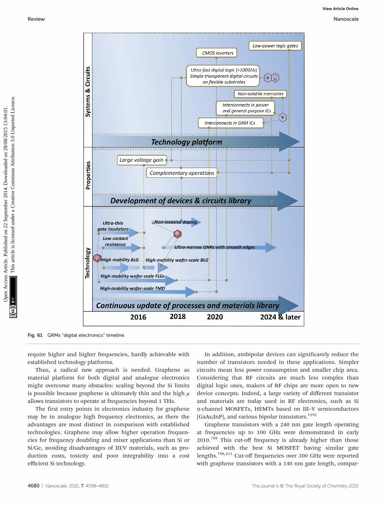
require higher and higher frequencies, hardly achievable withestablished technology platforms.
Thus, a radical new approach is needed. Graphene asmaterial platform for both digital and analogue electronicsmight overcome many obstacles: scaling beyond the Si limitsis possible because graphene is ultimately thin and the high μ
allows transistors to operate at frequencies beyond 1 THz.The first entry points in electronics industry for graphene
may be in analogue high frequency electronics, as there theadvantages are most distinct in comparison with establishedtechnologies. Graphene may allow higher operation frequen-cies for frequency doubling and mixer applications than Si orSi/Ge, avoiding disadvantages of III/V materials, such as pro-duction costs, toxicity and poor integrability into a costefficient Si technology.
In addition, ambipolar devices can significantly reduce thenumber of transistors needed in these applications. Simplercircuits mean less power consumption and smaller chip area.Considering that RF circuits are much less complex thandigital logic ones, makers of RF chips are more open to newdevice concepts. Indeed, a large variety of different transistorand materials are today used in RF electronics, such as Sin-channel MOSFETs, HEMTs based on III–V semiconductors(GaAs;InP), and various bipolar transistors.1192
Graphene transistors with a 240 nm gate length operatingat frequencies up to 100 GHz were demonstrated in early2010.788 This cut-off frequency is already higher than thoseachieved with the best Si MOSFET having similar gatelengths.788,433 Cut-off frequencies over 300 GHz were reportedwith graphene transistors with a 140 nm gate length, compar-
Fig. 61 GRMs “digital electronics” timeline.
Review Nanoscale
4680 | Nanoscale, 2015, 7, 4598–4810 This journal is © The Royal Society of Chemistry 2015
Ope
n A
cces
s A
rtic
le. P
ublis
hed
on 2
2 Se
ptem
ber
2014
. Dow
nloa
ded
on 2
8/08
/201
5 13
:04:
01.
Thi
s ar
ticle
is li
cens
ed u
nder
a C
reat
ive
Com
mon
s A
ttrib
utio
n 3.
0 U
npor
ted
Lic
ence
.View Article Online

able with the very top HEMTs transistors with similar gatelengths.1197 More recently, a cut-off frequency of 427 GHz wasextracted for a 67 nm channel length graphene transistor,1198
see Fig. 62. These results are impressive, comparing the youngage of graphene with the longer timescales of other devices.This is also a clear indication that GFETs have the potential topass the THz-border in the near future. Thus, graphene mayoffer a cost efficient platform for novel applications in a varietyof fields, such spectroscopy or automotive radar in analoguehigh frequency electronics. Significant impact in analogue RFcommunication electronics in areas as diverse as low noiseamplifiers, frequency multipliers, mixers and oscillators couldbe achieved within the next 10 years, see the timeline in Fig. 67.
Research efforts will not only be required for the optimiz-ation of graphene-based devices, but also for the developmentof circuit designs that can fully exploit the unique propertiesof graphene-based devices. The absence of a band-gap, there-with the un-incisive current saturation, the ambipolarity andthe targeted operation frequencies going beyond 100 GHzrequire new concepts on system level and circuit design, whichcould also open the door towards novel functionalities. Thus,to take advantage of the full potential of graphene devices, theaim is to combine more basic research with improved materialgrowth and device technology. A better understanding of para-meters such as breakdown voltage, electron velocity, and satur-ation current is needed to allow a complete benchmark of thismaterial and an evaluation of its potential performance. In
addition, these new applications will have to overcome thelimitations that arise from the lack of band-gap.
Once the growth and fabrication technology matures, themain challenges for RF applications are the integration of gra-phene devices in Si technology, and the increase of their trans-conductance by, e.g., introducing a band gap, and ensuringsufficient Av and output currents so that components can beintegrated to circuits.
For real applications not only the cut-off frequency is animportant figure of merit; Av and fmax, the frequency where theunilateral power gain reaches unity, are even more important.Both of these quantities are much more sensitive on theprocess technology than the cut-off frequency. In graphenetransistors Av and fmax still lag behind established techno-logies. Therefore, much effort on developing the process tech-nology is required. Additionally, integrated circuits of highercomplexity have not been realized so far, because the requiredprocess technology is still in its embryonic stage and circuitscan hardly be designed, as a parameter library for graphene-based devices is still missing.
Advanced graphene devices have the potential to transformcommunication systems in a broad array of new applicationsin the next 20 years. Graphene is therefore in an excellent posi-tion to help RF systems become even more ubiquitous and ver-satile than they are today.
5.3.1. Analogue voltage amplifiers. The main buildingblock of analogue electronics is a voltage amplifier: an elec-tronic device capable of amplifying small AC voltage signals.For the same reasons discussed in section 5.2.1 in case ofdigital logic gates, AC Av is usually much less than unity in gra-phene circuits. The use of GFETs in analogue electronics iscurrently limited to niche applications, such as analoguemixers,1199 but even these require voltage amplifiers for signalprocessing. RT operation of GFETs with a high Av is of para-mount importance; otherwise, graphene circuits and detectorsshould be destined to rely on Si FETs for signal amplificationand processing.1200 This is not favourably viewed by the semi-conductor industry, which generally does not like expensivehybrid technologies.
One of the main factors contributing to a low Av is the useof back-gated Si/SiO2 devices, which also suffer from largeparasitic capacitances and cannot be integrated with othercomponents. For this reason, top-gated GFETs with thinnergate insulators were extensively investigated,1201 as in case ofdigital logic gates.
The future investigation of graphene voltage amplifierspartly overlaps with that of digital logic gates, as in both casesthe short-term goal is the same: large Av > 10 should beobtained in wafer-scale SLG and BLG grown by CVD or on SiCsubstrates. In order to further increase Av, FETs should be fab-ricated from wafer-scale BLGs. Finally, several remaining chal-lenges of GFETs, technological rather than fundamental innature, should be addressed. E.g., graphene circuits remainsensitive to fabrication induced variability. Higher μ, gm andlower gd and contact resistance should increase Av for bothanalogue and digital applications. The long-term goal should
Fig. 62 Cut-off frequency versus gate length for GFETs, nanotube FETsand three types of RF-FETs [Adapted from ref. 1193]. pHEMT = pseudo-morphic HEMT, mHEMT = metamorphic HEMT. HEMTs are made of het-erojunctions, i.e., junctions of different materials.1194,1195 The mostcommon example are GaAs HEMTs in which there are junctionsbetween AlxGa(1−x)As and GaAs. Different materials have different latticeconstants, hence crystal defects are expected in HEMTs. In pHEMTs thisis avoided by using a very thin layer of one material1196 so that accumu-lated energy in this layer is not enough to relax the layer and introducedefects (energy is low because the layer is very thin).1196 In mHEMTs agraded buffer layer is used in between the layers to accommodate bothlattice constants1196 and eliminate the defects. E.g., to grow Al0.3Ga0.7Ason GaAs, an AlxGa(1−x)As layer is grown first in which x = 0 at the begin-ning (GaAs) and then x is gradually increased to 0.3 (Al0.3Ga0.7As).
1196
Nanoscale Review
This journal is © The Royal Society of Chemistry 2015 Nanoscale, 2015, 7, 4598–4810 | 4681
Ope
n A
cces
s A
rtic
le. P
ublis
hed
on 2
2 Se
ptem
ber
2014
. Dow
nloa
ded
on 2
8/08
/201
5 13
:04:
01.
Thi
s ar
ticle
is li
cens
ed u
nder
a C
reat
ive
Com
mon
s A
ttrib
utio
n 3.
0 U
npor
ted
Lic
ence
.View Article Online

be the integration of graphene amplifiers in more complex(i.e., multi-stage) analogue circuits.
GFETs are well suited as building blocks of low-noise ampli-fiers (LNAs) as they exhibit very low levels of electronic flickernoise102 (or 1/f noise, where f is the frequency, occurring inalmost all electronic devices and related to a direct current: aresistance fluctuation, which is transformed to voltage orcurrent fluctuations via Ohm’s law) which dominates the noisespectrum at low frequencies.1202–1204 Such voltage amplifiersare also expected to benefit from graphene’s high mechanicaland chemical stability and high κ.102 Graphene LNAs areneeded in high-frequency electronics,1205,1206 as their realiz-ation would allow seamless integration with graphene ana-logue mixers, thus eliminating need for Si FETs in theseapplications. As present, GFETs cannot be turned off, thusclass-A amplifiers (i.e. amplifiers which conduct during thewhole input cycle) with low harmonic distortions should bedeveloped. Large Av may allow realization of electronic harmo-nic oscillators, combining high-Av amplifiers with passive gra-phene feedback networks.
The development of graphene voltage amplifiers could pavethe way for graphene power amplifiers. These are usuallyfound in the final stages of more complex amplifiers. Theyoperate with Av = 1 and have a sole purpose to match the pre-viously amplified signals (provided by the voltage amplifiers)to a low-impedance load, such as a loudspeaker (∼4 Ω) inhigh-fidelity audio systems1207 or antenna of a transmitter(∼50 Ω) in RF applications.
The timeline is shown in Fig. 67. 3–4 years: LNAs. 4–5 years:Audio and RF voltage amplifiers. 5–6 years: Harmonic oscil-lators. 5–10 years: Power amplifiers.
5.3.2. Graphene ring oscillators. GROs1102,1155,1208 are anextension of cascaded graphene inverters.1144 Each inverter inthe loop must be identical, with Av > 1 and in/out signalmatching. The two FETs in each inverter must also have verylow on-state resistance to be able to quickly charge/dischargethe gate capacitance of the next stage in order to reach high-frequency operation. Since the oscillation frequency fo is adirect measure of delays in realistic scenarios, ROs are thestandard test-beds for evaluating ultimate limits and clockrates of digital logic families.1209 This is because a realisticelectronic circuit is both driven and loaded by other electroniccircuits, exactly what exists in a RO; in contrast, fT is measuredon a single FET which is driven by an ideal current source andhas a shorted output (zero load impedance). The ROs inFig. 63 were fully integrated on CVD graphene.1102
Complementary operation of the inverters within a RO wasobtained between the Dirac points of two GFETs1102, as in earlygraphene inverters.1149 These inverters have Av > 4, enough toenable oscillations under signal matching. The oscillation fre-quency of a RO with n stages cascaded in a loop is inverselyproportional to the inverter rise/fall delays τ as fo = 1/(2nτ) =fo1,
1210 where fo1 is a fan-out of one (FO1) oscillation frequency,where fan-out is the number of digital inputs that the output ofa single logic gate can feed. Since τ ∼ CGD
−1,1102 with GD thesum of extrinsic drain conductances of the GFETs in the inver-
ter and C the parasitic capacitive load of the inverter, reductionof parasitics leads to high-frequency operation.
The speed of electronic circuits is typically increased bydownscaling their dimensions,12 which also reduces parasitics(because parasitic capacitances are proportional to the surfacearea of the corresponding device parts). This is demonstratedin Fig. 64, plotting the maximum oscillation frequency of 26GROs as a function of gate length L. The highest is fo = 1.28GHz at L = 1 μm, corresponding to a FO1 τ ∼ 100 ps. This issimilar to that of conventional Si CMOS ROs,1211 and smallerthan polycrystalline Si CMOS thin-film ROs1212 for the same L.This is the first operating frequency above 1 GHz in digital cir-cuits based on any type of novel low-dimensional materials(e.g. nanotubes, nanowires, graphene, MoS2). By comparison,the highest frequency of nanotube ROs was ∼50 MHz,1213 and1.6 MHz in 2L-MoS2 ROs.
1214
The dependence of the oscillation frequency of convention-al ROs on the supply voltage is a serious problem in complexdigital circuits, since increased power consumption placesstrong demand on the supply voltage causing it to fluctu-ate.1215 Such fluctuations degrade the operation of logic gatesand their noise performance.1215 In contrast to other types ofROs, GROs are much less sensitive to fluctuations in thesupply voltage, as a consequence of their reduced voltage
Fig. 63 Integrated GRO. (a) Circuit diagram of a three-stage RO. TheRO comprises three inverters (1–3) cascaded in a loop with a fourthinverter (4) decoupling the RO from the measurement equipment con-nected to the output (out). (b) Optical microscope image of a RO withgate length L = 1 μm integrated on a CVD graphene channel. The draincontacts of inverters 1–3 (Au) overlap with the gate contacts (Al/Ti/Au)in order to form internal connections between the inverters. GND =ground. Adapted from ref. 1102.
Review Nanoscale
4682 | Nanoscale, 2015, 7, 4598–4810 This journal is © The Royal Society of Chemistry 2015
Ope
n A
cces
s A
rtic
le. P
ublis
hed
on 2
2 Se
ptem
ber
2014
. Dow
nloa
ded
on 2
8/08
/201
5 13
:04:
01.
Thi
s ar
ticle
is li
cens
ed u
nder
a C
reat
ive
Com
mon
s A
ttrib
utio
n 3.
0 U
npor
ted
Lic
ence
.View Article Online
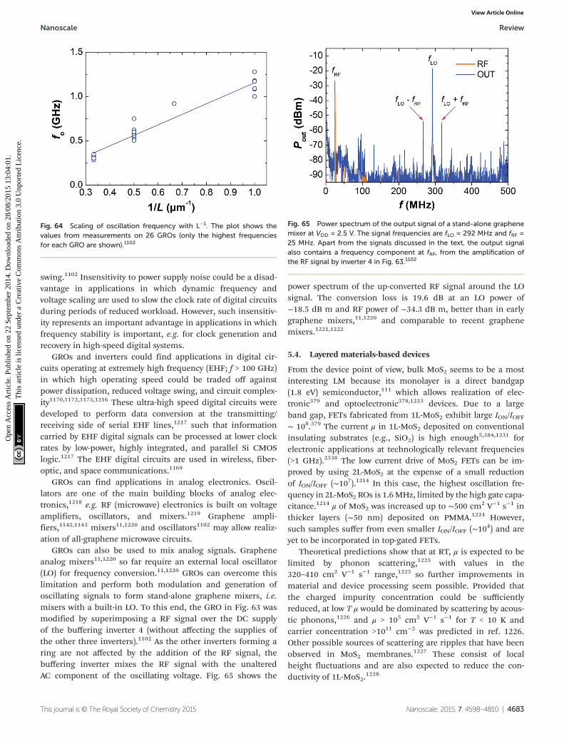
swing.1102 Insensitivity to power supply noise could be a disad-vantage in applications in which dynamic frequency andvoltage scaling are used to slow the clock rate of digital circuitsduring periods of reduced workload. However, such insensitiv-ity represents an important advantage in applications in whichfrequency stability is important, e.g. for clock generation andrecovery in high-speed digital systems.
GROs and inverters could find applications in digital cir-cuits operating at extremely high frequency (EHF; f > 100 GHz)in which high operating speed could be traded off againstpower dissipation, reduced voltage swing, and circuit complex-ity1170,1172,1173,1216 These ultra-high speed digital circuits weredeveloped to perform data conversion at the transmitting/receiving side of serial EHF lines,1217 such that informationcarried by EHF digital signals can be processed at lower clockrates by low-power, highly integrated, and parallel Si CMOSlogic.1217 The EHF digital circuits are used in wireless, fiber-optic, and space communications.1169
GROs can find applications in analog electronics. Oscil-lators are one of the main building blocks of analog elec-tronics,1218 e.g. RF (microwave) electronics is built on voltageamplifiers, oscillators, and mixers.1219 Graphene ampli-fiers,1142,1143 mixers11,1220 and oscillators1102 may allow realiz-ation of all-graphene microwave circuits.
GROs can also be used to mix analog signals. Grapheneanalog mixers11,1220 so far require an external local oscillator(LO) for frequency conversion.11,1220 GROs can overcome thislimitation and perform both modulation and generation ofoscillating signals to form stand-alone graphene mixers, i.e.mixers with a built-in LO. To this end, the GRO in Fig. 63 wasmodified by superimposing a RF signal over the DC supplyof the buffering inverter 4 (without affecting the supplies ofthe other three inverters).1102 As the other inverters forming aring are not affected by the addition of the RF signal, thebuffering inverter mixes the RF signal with the unalteredAC component of the oscillating voltage. Fig. 65 shows the
power spectrum of the up-converted RF signal around the LOsignal. The conversion loss is 19.6 dB at an LO power of−18.5 dB m and RF power of −34.3 dB m, better than in earlygraphene mixers,11,1220 and comparable to recent graphenemixers.1221,1222
5.4. Layered materials-based devices
From the device point of view, bulk MoS2 seems to be a mostinteresting LM because its monolayer is a direct bandgap(1.8 eV) semiconductor,111 which allows realization of elec-tronic379 and optoelectronic378,1223 devices. Due to a largeband gap, FETs fabricated from 1L-MoS2 exhibit large ION/IOFF∼ 108.379 The current μ in 1L-MoS2 deposited on conventionalinsulating substrates (e.g., SiO2) is high enough5,384,1231 forelectronic applications at technologically relevant frequencies(>1 GHz).2338 The low current drive of MoS2 FETs can be im-proved by using 2L-MoS2 at the expense of a small reductionof ION/IOFF (∼107).1214 In this case, the highest oscillation fre-quency in 2L-MoS2 ROs is 1.6MHz, limited by the high gate capa-citance.1214 μ of MoS2 was increased up to ∼500 cm2 V−1 s−1 inthicker layers (∼50 nm) deposited on PMMA.1224 However,such samples suffer from even smaller ION/IOFF (∼104) and areyet to be incorporated in top-gated FETs.
Theoretical predictions show that at RT, μ is expected to belimited by phonon scattering,1225 with values in the320–410 cm2 V−1 s−1 range,1225 so further improvements inmaterial and device processing seem possible. Provided thatthe charged impurity concentration could be sufficientlyreduced, at low T μ would be dominated by scattering by acous-tic phonons,1226 and μ > 105 cm2 V−1 s−1 for T < 10 K andcarrier concentration >1011 cm−2 was predicted in ref. 1226.Other possible sources of scattering are ripples that have beenobserved in MoS2 membranes.1227 These consist of localheight fluctuations and are also expected to reduce the con-ductivity of 1L-MoS2.
1228
Fig. 65 Power spectrum of the output signal of a stand-alone graphenemixer at VDD = 2.5 V. The signal frequencies are fLO = 292 MHz and fRF =25 MHz. Apart from the signals discussed in the text, the output signalalso contains a frequency component at fRF, from the amplification ofthe RF signal by inverter 4 in Fig. 63.1102
Fig. 64 Scaling of oscillation frequency with L−1. The plot shows thevalues from measurements on 26 GROs (only the highest frequenciesfor each GRO are shown).1102
Nanoscale Review
This journal is © The Royal Society of Chemistry 2015 Nanoscale, 2015, 7, 4598–4810 | 4683
Ope
n A
cces
s A
rtic
le. P
ublis
hed
on 2
2 Se
ptem
ber
2014
. Dow
nloa
ded
on 2
8/08
/201
5 13
:04:
01.
Thi
s ar
ticle
is li
cens
ed u
nder
a C
reat
ive
Com
mon
s A
ttrib
utio
n 3.
0 U
npor
ted
Lic
ence
.View Article Online

1L-MoS2 devices exhibit n-type transport behaviour. Ambi-polar transport was demonstrated in thin (10 nm) MoS2 electri-cal double-layer transistor using an ionic liquid as the gate.1229
The demonstration of both p and n-type transport in devicesbased on solid-state dielectrics would be useful for appli-cations in CMOS-type logic and pn-junctions for optoelectronicdevices. The use of liquid gates has also recently allowed largecharge carrier concentrations in 10 nm thick MoS2 and gate-tunable superconductivity.1230 Metal-insulator transitionin 1L-MoS2 Hall-bars using classical dielectrics (HfO2) wasreported.1231
The presence of a band gap in MoS2 allows strongdrain current saturation, with drain-source conductance gds =dIds/dVds < 2 μS μm−1 demonstrated in 1L-MoS2,
1232 togetherwith high transconductance gm of 34 µS µm−1, which shouldallow high voltage gains for small signals (AV = gm/gds > 10).Such gains allowed the fabrication of digital circuits basedon MoS2, such as inverters,1044 ROs1214 as well as analogueamplifiers.1233
Transistors based on MoS2 can also operate with currentdensities of at least 4.9 × 10⁷ A cm−2,1232 50 times higher thanCu, comparing favourably to the breakdown current densityfor graphene on SiO2 (>10
8 A cm−2).103 This is due to intralayerMo–S covalent bonds being much stronger than metallicbonds. Such high breakdown current density would allowaggressive downscaling of MoS2 devices. Integration with highκ substrates, such as diamond,199 could result in furtherincrease of breakdown current density.
Device simulations of 1L-MoS2 transistors425,1234 predictthat 1L-MoS2 would show superior resistance to short-channeleffects due to its small thickness. These calculations show thattop-gated MoS2 transistors with gate lengths of 15 nm couldoperate in the ballistic regime with on-current as high as1.6 mA μm−1, subthreshold swing close to 60 mV dec−1 andION/IOFF ∼ 1010. Although MoS2 will probably not compete withconventional III–V transistors on μ values, attractive electricalperformance characteristics and high electrostatic controlcould make it and other TMDs viable candidates for appli-cations in low-power electronics.
The use of 2d materials could be very advantageous for therealization of memory devices based on the floating gate tran-sistor structure,1235,1236 used in flash memories. In this type ofdevice, the operation is based on detecting a threshold voltageshift caused by a presence or absence of charges trapped onthe floating gate. Decreasing the device size is limited by theamount of charge that can be stored on the floating gate.Using 1L-MoS2 or other 2d semiconductors as conductivechannels in such devices brings the benefit of increased sensi-tivity to external electric charge and could allow deeperscaling. Such devices based on 1L-MoS2 and graphene as keyelements were reported1235 in a geometry shown on Fig. 66.Graphene here acts as an ohmic-like contact, allowing efficientcharge carrier injection into MoS2 while multilayer graphene isused as the floating gate. The use of a 2d contact in place ofthicker metallic films is beneficial for several reasons. It allowsone to realize devices and circuits with 2d materials using
less expensive fabrication techniques, e.g. R2R printing, seesection 4.11.8.
The capacitive coupling between leads in neighbouringdevices is also reduced, allowing further scaling. Because of itsband gap and 2d nature, 1L-MoS2 is highly sensitive to thepresence of charges in the charge trapping layer, resulting in afactor of 104 difference between memory program and erasestates.1235 This allows a large memory window and the possi-bility to have different intermediate levels of charge in thefloating gate corresponding to multiple bits of information.
Several issues however still need to be addressed. There isat this point no control over intrinsic doping in MoS2 andmethods for introducing dopant atoms as well as achievingambipolar and p-type behaviour would be highly desirable.Understanding how to make good electrical contacts to MoS2is also lagging and it is not clear yet which material and con-tacting scheme would result in the smallest possible contactresistance.
Few-layer phosphorene116,1237 has been investigated as anew 2d p-type electronic material. Few-layer phosphorene isstable, having a direct band-gap that depends on the numberof layers,116 going from ∼2 eV in monolayer to ∼0.3 eV inbulk.1237 Phosphorene field-effect transistors with 1 μmchannel length have shown a RT μ (hole) ∼ 286 cm2 V−1 s−1,and ION/IOFF up to 104.116 Ref. 1237 reported that μ in few-layerphosphorene is thickness-dependent, with the highestachieved values of ∼1000 cm2 V−1 s−1 obtained for ∼10 nmsamples at RT. Although these results116,1237 demonstrate thepotential of few-layer phosphorene as a new 2d material forapplications in nanoelectronic devices, these are only the firstreports and more work is needed to fully assess this material.
5.5. Novel vertical and planar transistors and devices
2d heterostructures offer richer opportunities in terms ofphysics and transport properties than each of the individual2d crystals. The most obvious device to develop is the TFET.106
Initial results indicate that such devices will indeed offerrequired parameters in terms of ION/IOFF and μ. Other direc-tions to explore, both experimentally and theoretically, are hot
Fig. 66 MoS2/graphene heterostructure memory layout. 3d schematicview of the memory device based on 1L-MoS2 semiconducting channel,SLG contacts and FLG floating gate. The FLG floating gate is separatedfrom the channel by a thin tunnelling oxide and from the control gate bya thicker blocking oxide.
Review Nanoscale
4684 | Nanoscale, 2015, 7, 4598–4810 This journal is © The Royal Society of Chemistry 2015
Ope
n A
cces
s A
rtic
le. P
ublis
hed
on 2
2 Se
ptem
ber
2014
. Dow
nloa
ded
on 2
8/08
/201
5 13
:04:
01.
Thi
s ar
ticle
is li
cens
ed u
nder
a C
reat
ive
Com
mon
s A
ttrib
utio
n 3.
0 U
npor
ted
Lic
ence
.View Article Online

electrons transistors, resonant tunnelling and formation ofminibands.
Planar devices can include double quantum wells, drag inparallel 2d electron gases, Bose–Einstein condensation in suchsystems, etc. Also, effects of enhancement of electronic pro-perties (improved μ) for each individual conductive layer needto be addressed.
Exotic combinations, such as superconductor/insulator/normal metal or superconductor/insulator/ferromagnet, oreven more complex structures, providing one can find suitable2d crystals, need investigation. Such devices would allow theexploration of quasi-particles spin and valley degrees offreedom. By embedding nanoclusters of conventional metals,ferromagnets, and semiconductors between the layers, it maybe possible to combine the opportunities for quantum techno-
logies offered by the QD physics and the unique electronic pro-perties of 2d heterostructures.
5.5.1. Vertical tunnelling transistors and vertical hot elec-tron transistors. The vertical tunnelling transistor106 is a viablealternative to the current approach to graphene-based elec-tronics. Rapid response and ultra-small sizes can also beachieved in vertical transistors. Electron transfer through nmthick barriers can be extremely fast (possibly coherent). Ballistictunnelling transistors may allow to overcome the current lowION/IOFF. Tunnelling devices would have a highly insulated offstate with no dissipation, which should allow not only individualtransistors, but integrated circuits at RT. The latter is difficultto achieve for horizontal transport and remains a distant goal.
The aim is to explore, by experiments and modelling,several architectures for tunnelling/hot electron transistors.
Fig. 67 High frequency electronics timeline.
Nanoscale Review
This journal is © The Royal Society of Chemistry 2015 Nanoscale, 2015, 7, 4598–4810 | 4685
Ope
n A
cces
s A
rtic
le. P
ublis
hed
on 2
2 Se
ptem
ber
2014
. Dow
nloa
ded
on 2
8/08
/201
5 13
:04:
01.
Thi
s ar
ticle
is li
cens
ed u
nder
a C
reat
ive
Com
mon
s A
ttrib
utio
n 3.
0 U
npor
ted
Lic
ence
.View Article Online
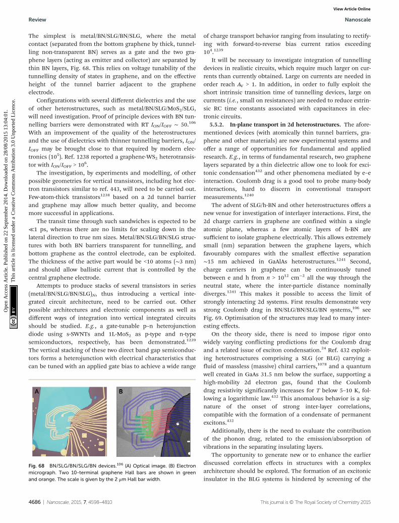
The simplest is metal/BN/SLG/BN/SLG, where the metalcontact (separated from the bottom graphene by thick, tunnel-ling non-transparent BN) serves as a gate and the two gra-phene layers (acting as emitter and collector) are separated bythin BN layers, Fig. 68. This relies on voltage tunability of thetunnelling density of states in graphene, and on the effectiveheight of the tunnel barrier adjacent to the grapheneelectrode.
Configurations with several different dielectrics and the useof other heterostructures, such as metal/BN/SLG/MoS2/SLG,will need investigation. Proof of principle devices with BN tun-nelling barriers were demonstrated with RT ION/IOFF ∼ 50.106
With an improvement of the quality of the heterostructuresand the use of dielectrics with thinner tunnelling barriers, ION/IOFF may be brought close to that required by modern elec-tronics (105). Ref. 1238 reported a graphene-WS2 heterotransis-tor with ION/IOFF > 106.
The investigation, by experiments and modelling, of otherpossible geometries for vertical transistors, including hot elec-tron transistors similar to ref. 443, will need to be carried out.Few-atom-thick transistors1238 based on a 2d tunnel barrierand graphene may allow much better quality, and becomemore successful in applications.
The transit time through such sandwiches is expected to be≪1 ps, whereas there are no limits for scaling down in thelateral direction to true nm sizes. Metal/BN/SLG/BN/SLG struc-tures with both BN barriers transparent for tunnelling, andbottom graphene as the control electrode, can be exploited.The thickness of the active part would be <10 atoms (∼3 nm)and should allow ballistic current that is controlled by thecentral graphene electrode.
Attempts to produce stacks of several transistors in series(metal/BN/SLG/BN/SLG)N, thus introducing a vertical inte-grated circuit architecture, need to be carried out. Otherpossible architectures and electronic components as well asdifferent ways of integration into vertical integrated circuitsshould be studied. E.g., a gate-tunable p–n heterojunctiondiode using s-SWNTs and 1L-MoS2 as p-type and n-typesemiconductors, respectively, has been demonstrated.1239
The vertical stacking of these two direct band gap semiconduc-tors forms a heterojunction with electrical characteristics thatcan be tuned with an applied gate bias to achieve a wide range
of charge transport behavior ranging from insulating to rectify-ing with forward-to-reverse bias current ratios exceeding104.1239
It will be necessary to investigate integration of tunnellingdevices in realistic circuits, which require much larger on cur-rents than currently obtained. Large on currents are needed inorder reach AV > 1. In addition, in order to fully exploit theshort intrinsic transition time of tunnelling devices, large oncurrents (i.e., small on resistances) are needed to reduce extrin-sic RC time constants associated with capacitances in elec-tronic circuits.
5.5.2. In-plane transport in 2d heterostructures. The afore-mentioned devices (with atomically thin tunnel barriers, gra-phene and other materials) are new experimental systems andoffer a range of opportunities for fundamental and appliedresearch. E.g., in terms of fundamental research, two graphenelayers separated by a thin dielectric allow one to look for exci-tonic condensation432 and other phenomena mediated by e–einteraction. Coulomb drag is a good tool to probe many-bodyinteractions, hard to discern in conventional transportmeasurements.1240
The advent of SLG/h-BN and other heterostructures offers anew venue for investigation of interlayer interactions. First, the2d charge carriers in graphene are confined within a singleatomic plane, whereas a few atomic layers of h-BN aresufficient to isolate graphene electrically. This allows extremelysmall (nm) separation between the graphene layers, whichfavourably compares with the smallest effective separation∼15 nm achieved in GaAlAs heterostructures.1241 Second,charge carriers in graphene can be continuously tunedbetween e and h from n > 1012 cm−2 all the way through theneutral state, where the inter-particle distance nominallydiverges.1241 This makes it possible to access the limit ofstrongly interacting 2d systems. First results demonstrate verystrong Coulomb drag in BN/SLG/BN/SLG/BN systems,106 seeFig. 69. Optimisation of the structures may lead to many inter-esting effects.
On the theory side, there is need to impose rigor ontowidely varying conflicting predictions for the Coulomb dragand a related issue of exciton condensation.24 Ref. 432 exploit-ing heterostructures comprising a SLG (or BLG) carrying afluid of massless (massive) chiral carriers,1078 and a quantumwell created in GaAs 31.5 nm below the surface, supporting ahigh-mobility 2d electron gas, found that the Coulombdrag resistivity significantly increases for T below 5–10 K, fol-lowing a logarithmic law.432 This anomalous behavior is a sig-nature of the onset of strong inter-layer correlations,compatible with the formation of a condensate of permanentexcitons.432
Additionally, there is the need to evaluate the contributionof the phonon drag, related to the emission/absorption ofvibrations in the separating insulating layers.
The opportunity to generate new or to enhance the earlierdiscussed correlation effects in structures with a complexarchitecture should be explored. The formation of an excitonicinsulator in the BLG systems is hindered by screening of the
Fig. 68 BN/SLG/BN/SLG/BN devices.106 (A) Optical image. (B) Electronmicrograph. Two 10-terminal graphene Hall bars are shown in greenand orange. The scale is given by the 2 μm Hall bar width.
Review Nanoscale
4686 | Nanoscale, 2015, 7, 4598–4810 This journal is © The Royal Society of Chemistry 2015
Ope
n A
cces
s A
rtic
le. P
ublis
hed
on 2
2 Se
ptem
ber
2014
. Dow
nloa
ded
on 2
8/08
/201
5 13
:04:
01.
Thi
s ar
ticle
is li
cens
ed u
nder
a C
reat
ive
Com
mon
s A
ttrib
utio
n 3.
0 U
npor
ted
Lic
ence
.View Article Online

Coulomb interaction, which appears to be sensitive to the elec-tron spin and valley degeneracy. The T of the excitonic insula-tor transition in MoS2/(BN)n/MoS2 sandwiches may be higherand fall into the experimentally accessible range. Also, thesearch for correlated states in NbSe2/(BN)n/NbSe2 sandwichesshould be undertaken, since these, by extrapolating from bulkproperties of NbSe2 (ref. 1242), may form both charge densitywaves and superconductivity.
5.6. Electron emission
“Vacuum microelectronics” has been of interest since the1970s.1243,1244 Its development was initially driven by theaspiration to create new, more efficient, forms of electronicinformation display known as “field effect (FE) displays”1245 or“nano-emissive displays”.1245 Even though prototypes havebeen demonstrated,1245 the development of such displays intoreliable commercial products has been hindered by a variety ofindustrial production problems, essentially related to individu-ally addressable sub-pixels technology, not directly related tothe source characteristics. However, after considerable timeand effort, many companies are now shutting down theireffort to develop this technology commercially. This is essen-tially connected with the huge development of both flat-panelliquid crystal and organic light emitting diode (OLED) dis-plays. Nevertheless, in January 2010, AU Optronics acquired FEdisplay assets from Sony continuing the development of thistechnology.1246 Large-area FE sources involve many otherapplications, ranging from microwave and X-ray generation,space-vehicle neutralization and multiple e-beam lithographyto plastic electronics.
The early devices were essentially the “Spindt array”,1243
and the “Latham emitter”.1247 The first used Si-integrated-circuit fabrication techniques to create regular arrays whereMo cones were deposited in cylindrical voids in an oxide film,with the void covered by a counter-electrode (CE) with a centralcircular aperture. In order to avoid IC fabrication the Lathamemitters were developed.1247 These comprise two differentdevices, the metal–insulator–metal–insulator–vacuum and the
conductor–dielectric–conductor–dielectric–vacuum.1247 Thelatter contained conducting particulates in a dielectric filmand the FE is assured by the field-enhancing properties of themicro/nanostructures.
Nowadays this research area targets the development/inves-tigation of new nanomaterials that could be grown/depositedon suitable substrate as thin films with appropriate FE pro-perties. In a parallel-plate arrangement, the field between theplates (FM) is given by FM = V/W, where V is the appliedvoltage and W is the plate distance. If a sharp object is grown/deposited on one plate, then the local field F at its apex isgreater than FM and can be related to FM by: F = ζFM. Theparameter ζ is called the “field enhancement factor” and isessentially determined by the object’s shape.1248 Because FEcharacteristics are determined by F, the higher ζ, the lower FMand, for a given W, the lower V at which field emission occurs.
FE from amorphous, “diamond-like” carbon1249,1250 andnanostructured carbon films1251,1252 has been investigated fordecades. The introduction of CNT-FEs,1253–1256 was a signifi-cant step forward, with extensive research carried out both fortheir physical characteristics and possible technologicalapplications.1253–1256 In recent years there has also been inter-est in the development of nanostructures, with a sufficientlyhigh density of individual emission sites based on othercarbon forms such as “carbon nanowalls”1257 and on variousforms of wide-band-gap semiconductor.1258
Graphene has atomic thickness, high aspect ratio (ratio oflateral size to thickness), excellent σ, and good mechanical pro-perties, which qualify it as an attractive candidate as FEsource.1259–1262 Carbon has one of the lowest sputter coeffi-cients,1263 which is an advantage as an electron source isusually bombarded by positive ions. Consequently, thanks tothe aforementioned properties, an enhanced local electricfield and good electron-emission stability can be expected forgraphene (Fig. 70).
The presence of edges may render graphene superior toCNTs for tunnelling of electrons.1260 Indeed, the atoms at gra-phene edges can have an unconventional electronic struc-
Fig. 69 (A) Tunnelling I–V s and their response to gate voltage (in 5 V steps) for a BN/SLG/(BN)4/SLG/BN device.106 T = 300 K. (B) Changes in low-bias tunnelling (symbols) and the theory fit for 4 hBN layers (solid curve). Adapted from ref. 106.
Nanoscale Review
This journal is © The Royal Society of Chemistry 2015 Nanoscale, 2015, 7, 4598–4810 | 4687
Ope
n A
cces
s A
rtic
le. P
ublis
hed
on 2
2 Se
ptem
ber
2014
. Dow
nloa
ded
on 2
8/08
/201
5 13
:04:
01.
Thi
s ar
ticle
is li
cens
ed u
nder
a C
reat
ive
Com
mon
s A
ttrib
utio
n 3.
0 U
npor
ted
Lic
ence
.View Article Online
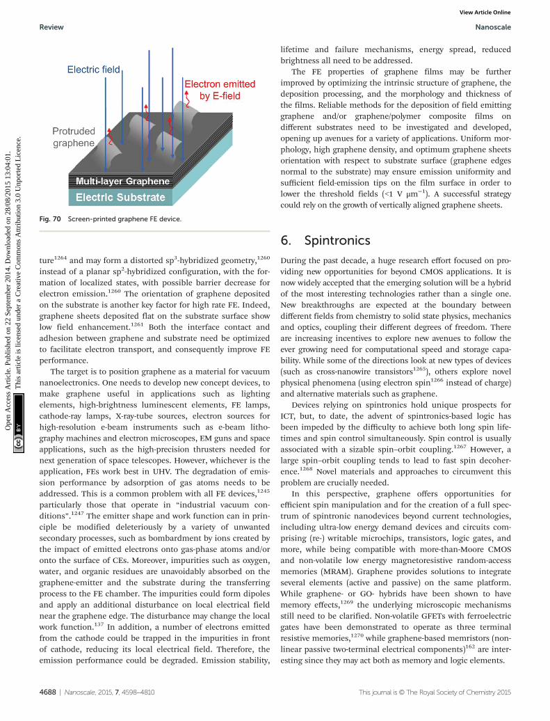
ture1264 and may form a distorted sp3-hybridized geometry,1260
instead of a planar sp2-hybridized configuration, with the for-mation of localized states, with possible barrier decrease forelectron emission.1260 The orientation of graphene depositedon the substrate is another key factor for high rate FE. Indeed,graphene sheets deposited flat on the substrate surface showlow field enhancement.1261 Both the interface contact andadhesion between graphene and substrate need be optimizedto facilitate electron transport, and consequently improve FEperformance.
The target is to position graphene as a material for vacuumnanoelectronics. One needs to develop new concept devices, tomake graphene useful in applications such as lightingelements, high-brightness luminescent elements, FE lamps,cathode-ray lamps, X-ray-tube sources, electron sources forhigh-resolution e-beam instruments such as e-beam litho-graphy machines and electron microscopes, EM guns and spaceapplications, such as the high-precision thrusters needed fornext generation of space telescopes. However, whichever is theapplication, FEs work best in UHV. The degradation of emis-sion performance by adsorption of gas atoms needs to beaddressed. This is a common problem with all FE devices,1245
particularly those that operate in “industrial vacuum con-ditions”.1247 The emitter shape and work function can in prin-ciple be modified deleteriously by a variety of unwantedsecondary processes, such as bombardment by ions created bythe impact of emitted electrons onto gas-phase atoms and/oronto the surface of CEs. Moreover, impurities such as oxygen,water, and organic residues are unavoidably absorbed on thegraphene-emitter and the substrate during the transferringprocess to the FE chamber. The impurities could form dipolesand apply an additional disturbance on local electrical fieldnear the graphene edge. The disturbance may change the localwork function.137 In addition, a number of electrons emittedfrom the cathode could be trapped in the impurities in frontof cathode, reducing its local electrical field. Therefore, theemission performance could be degraded. Emission stability,
lifetime and failure mechanisms, energy spread, reducedbrightness all need to be addressed.
The FE properties of graphene films may be furtherimproved by optimizing the intrinsic structure of graphene, thedeposition processing, and the morphology and thickness ofthe films. Reliable methods for the deposition of field emittinggraphene and/or graphene/polymer composite films ondifferent substrates need to be investigated and developed,opening up avenues for a variety of applications. Uniform mor-phology, high graphene density, and optimum graphene sheetsorientation with respect to substrate surface (graphene edgesnormal to the substrate) may ensure emission uniformity andsufficient field-emission tips on the film surface in order tolower the threshold fields (<1 V μm−1). A successful strategycould rely on the growth of vertically aligned graphene sheets.
6. Spintronics
During the past decade, a huge research effort focused on pro-viding new opportunities for beyond CMOS applications. It isnow widely accepted that the emerging solution will be a hybridof the most interesting technologies rather than a single one.New breakthroughs are expected at the boundary betweendifferent fields from chemistry to solid state physics, mechanicsand optics, coupling their different degrees of freedom. Thereare increasing incentives to explore new avenues to follow theever growing need for computational speed and storage capa-bility. While some of the directions look at new types of devices(such as cross-nanowire transistors1265), others explore novelphysical phenomena (using electron spin1266 instead of charge)and alternative materials such as graphene.
Devices relying on spintronics hold unique prospects forICT, but, to date, the advent of spintronics-based logic hasbeen impeded by the difficulty to achieve both long spin life-times and spin control simultaneously. Spin control is usuallyassociated with a sizable spin–orbit coupling.1267 However, alarge spin–orbit coupling tends to lead to fast spin decoher-ence.1268 Novel materials and approaches to circumvent thisproblem are crucially needed.
In this perspective, graphene offers opportunities forefficient spin manipulation and for the creation of a full spec-trum of spintronic nanodevices beyond current technologies,including ultra-low energy demand devices and circuits com-prising (re-) writable microchips, transistors, logic gates, andmore, while being compatible with more-than-Moore CMOSand non-volatile low energy magnetoresistive random-accessmemories (MRAM). Graphene provides solutions to integrateseveral elements (active and passive) on the same platform.While graphene- or GO- hybrids have been shown to havememory effects,1269 the underlying microscopic mechanismsstill need to be clarified. Non-volatile GFETs with ferroelectricgates have been demonstrated to operate as three terminalresistive memories,1270 while graphene-based memristors (non-linear passive two-terminal electrical components)162 are inter-esting since they may act both as memory and logic elements.
Fig. 70 Screen-printed graphene FE device.
Review Nanoscale
4688 | Nanoscale, 2015, 7, 4598–4810 This journal is © The Royal Society of Chemistry 2015
Ope
n A
cces
s A
rtic
le. P
ublis
hed
on 2
2 Se
ptem
ber
2014
. Dow
nloa
ded
on 2
8/08
/201
5 13
:04:
01.
Thi
s ar
ticle
is li
cens
ed u
nder
a C
reat
ive
Com
mon
s A
ttrib
utio
n 3.
0 U
npor
ted
Lic
ence
.View Article Online

6.1. Graphene spintronics
There are two fundamental properties of the electron whichare exploited in advanced technology – charge and spin – butconventionally their functions have been kept separated.1271
The charge is used in all electronic devices, particularly inlogic circuits, where current flows are controlled using electricfields, encoding and processing binary (or analogue) infor-mation. The spin is used in its “collective” form of magneticdomains for long-term data storage, from ferrite core mem-ories to modern hard drives.1271
This separation has begun to change with the advent ofspintronics, a relatively young field, the name itself havingbeen introduced only in 1996.23 This combines charge andspin of electrons in the solid state to create novel functional-ities. In the simplest spintronic device, called spin-valve,1272
an electronic current flows between two ferromagnetic electro-des through a non-magnetic channel carrying a spin signalalong with it, normally detected through its magnetoresis-tance,26 and its transport properties are influenced by mag-netic ordering. The requirement for non-magnetic channels isto transport spin currents, minimizing spin relaxation due tospin-scattering events that produce spin-information lossesthrough spin-flipping, ultimately (in most cases) caused byspin–orbit coupling.1273,1274
Graphene consists of light atoms, thus exhibits (in its pris-tine form) negligible spin–orbit coupling1275 and a possibleabsence of hyperfine interactions, due to the lack of nuclearspins in isotopically pure materials. These are the properties
required for high spin-signal conservation,1276 making gra-phene an interesting candidate for non-magnetic channels,with long spin relaxation and coherence times, the centralbenchmarks for spintronic devices.
Integration between graphene and other materials, includ-ing 2d crystals, shows great potential for further improve-ments. This includes, e.g., substrate optimisation, as shown bythe remarkable increase of spin relaxation length obtainedby depositing graphene on a BN substrate1277 or onFLG.223,1278–1280 However, from Hanle experiments (i.e. magne-toresistance measurements in which the spin is forced toprecess by an external magnetic field, while the magnetoresis-tance signal is monitored by spin diffusion length,223,1300 seeFig. 71), spin relaxation times have been reported to be in thens range for varying quality of graphene samples,1276 whereasthe spin relaxation mechanism is under debate, and a fullycomprehensive picture is still lacking.
Following what is known for metals and semiconductors,two mechanisms are currently believed to take place in gra-phene: Elliot–Yafet (EY)232,233 and Dyakonov–Perel (DP).162 InEY the electron spin has a finite probability to flip during eachscattering event off impurities or phonons.232,233 The DP mech-anism is driven by the precession of electron spins alongeffective magnetic field orientations, which depends on themomentum, and with direction and frequency of precessionchanging at each scattering event.162 The most recent theoreticalderivation in SLG (taking into account the Dirac cone physics)reports a spin relaxation time varying proportionally to thetransport time, behaviour typical of the EY-relaxation.1273
Fig. 71 (a) Typical two-terminal local spin valve device. The width of graphene channel on SiC is 10 µm, and the distance between the two Al2O3/Co electrodes is L = 2 µm. The optical image shows the entire structure, including contact pads. (b) Atomic arrangement of SLG on SiC. (c) Largelocal resistance spin signals measured at 4 K. (d) Oscillating and decaying device non-local resistance as a function of the applied magnetic field(Hanle measurement). Adapted from ref. 223, 1300.
Nanoscale Review
This journal is © The Royal Society of Chemistry 2015 Nanoscale, 2015, 7, 4598–4810 | 4689
Ope
n A
cces
s A
rtic
le. P
ublis
hed
on 2
2 Se
ptem
ber
2014
. Dow
nloa
ded
on 2
8/08
/201
5 13
:04:
01.
Thi
s ar
ticle
is li
cens
ed u
nder
a C
reat
ive
Com
mon
s A
ttrib
utio
n 3.
0 U
npor
ted
Lic
ence
.View Article Online
A primary objective in the near future is to clarify the truenature of the dominant mechanisms determining the spinrelaxation time and spin relaxation length in high quality gra-phene devices. Indeed, while spin transport in graphene hasbeen demonstrated by several groups worldwide, the fullunderstanding of spin dynamics and relaxation is still lacking,and theoretical predictions or generalization of the EY and DP-relaxation mechanisms seem unable to cope with the experi-mental reality.1276 Recent results indicate that the situationcan be improved by a precise tuning of the contact resistancebetween graphene and magnetic electrodes,223 but it is stillunclear what this implies for large scale RT devices. Moreeffort is thus needed in order to explore the spin relaxationmechanisms from a theoretical perspective beyond the con-ventional perturbative treatments. Spin relaxation time andthe g factor (or dimensionless magnetic moment) need to beevaluated by taking into account the relevant scattering pro-cesses close-to and away-from the Dirac point (short andlong range scatterers, e–e and e–ph interaction etc.), depend-ing on the intrinsic and extrinsic nature of scattering sources,and for the main classes of materials of relevance for RToperability.
Simultaneously, a global and comprehensive understandingof spin relaxation mechanisms needs to be established basedon the existing information and more targeted and systematicexperiments combining two-terminal magnetoresistance andfour terminal Hanle transport measurements (see Fig. 71) anddisentangling the contribution of contacts from intrinsic spinrelaxation induced by defects, disorder, interaction with sub-strate, etc. This is a major bottleneck, which demands a con-certed effort between experiment and theory.
6.2. Spin injection in graphene
The variety of favourable properties for spintronics that gra-phene provides include also efficient spin injection,223 due tothe tunability of the Fermi level. The large electron velocityimplies that graphene has unique properties for the transportof spin polarized currents to long distances.223 The analysis ofscattering mechanisms is necessary in order to achieveoptimal production methods for graphene-based spin-valves.The optimization of performances of graphene spin-valvedevices is required, comprising a focus on the specific role ofmagnetic contacts, including their spin injection and detec-tion efficiencies and the possible role of interface effects inspin relaxation and spin dephasing.
Interface engineering to optimize spin injection and detec-tion from a ferromagnet into graphene still remains a verychallenging issue and it represents one of the main bottle-necks. Systematic investigations of the role of the tunnelbarrier have been slow because of the difficulties of growinguniform, ultrathin insulating layers on graphene. Any irregu-larity during growth would favour the formation of pinholes.Alternative barriers and spin injection and detection methodsshould also be explored.
While in early devices spin injection was achieved usingtransparent contacts (Co/SLG),1281 a great improvement on
both injection efficiency and spin lifetime was obtained withtunnelling contacts (Co/Insulator/SLG).1282 One of the mainissues in conventional interfaces remains, however, the match-ing of conductances. For this purpose, interfaces of graphenewith graphite intercalated with magnetic impurities or mole-cules (similarly to magnetic semiconductors1283,1284) seemviable and have to be explored more deeply. The spin valve1285
is the natural bench to test the efficiency of spin injection withgraphene hybrids.1286 Further optimization of the ferro-magnetic contacts for both spin injection and detection is alsopossible. Currently, oxide tunnel barriers, such as Al2O3 andMgO, are common choices, but new barrier materials and newtechnologies based on (single) atomic layer deposition of BN,and related materials like MoS2 and MoSe2, to make tunnelbarriers of single or few atomic layer thicknesses, should beconsidered. Other concepts involving the spin Hall effect(SHE),234 which is the formation of spin-polarized currentdriven by spin–orbit coupling introduced by impurities,should also be explored;1287,1288 especially owing to the highlyefficient spin current generation observed in materials such asTa due to SHE.1289 Spin injection is currently performed anddeeply investigated in both SLG and BLG,1290 and measure-ments on FLG and MLG up to 40 nm thick have beenreported.1291–1293 Further experiments require unambiguousassessment of the potential of all of these and identifying, ineach case, the phenomena that determine the experimentallyobserved spin injection/detection efficiency. It is also crucialto investigate the integration between the graphene channeland different materials as substrates.
The development of new device fabrication and innovativespin manipulation protocols would advance spin injectionefficiency at the ferromagnet/graphene interfaces, data record-ing and spin information processing. More exciting is thedesign of novel spintronic devices at <10 nm scale. Here, com-ponents enter in the quantum regime, and graphene mayexploit the crossover between classical and quantum featuresof such nano-elements.
6.3. Graphene spintronic devices for sensing
The long spin diffusion length in graphene could enable itsuse in spintronic based magnetic sensors. It was shown1294
that graphene has a large non-local spin current effect nearthe Dirac point up to RT, and at small magnetic fields (0.1 T).Graphene spintronics has thus the potential to revolutionizethe development of magnetic sensors with sensitivity rangingfrom the nT to the pT ranges (for comparison, the Earth’smagnetic field is in the μT range1295). The potential of lab-on-chip spintronic sensors for magnetic nanoparticles would alsoimpact onsite drug delivery control or tumour disease fightmedicine. Additionally, breakthroughs in the fields of MRAMand reconfigurable logic have a cross-disciplinary interest forICT.1296 Intrinsic non-volatility of spintronics technologies pre-sents a significant advantage in terms of power consumption.The power consumption reduction will benefit as much fortightening supplies of energy, as for the digital societal revolu-tion of ever more demanding portable electronics. The radi-
Review Nanoscale
4690 | Nanoscale, 2015, 7, 4598–4810 This journal is © The Royal Society of Chemistry 2015
Ope
n A
cces
s A
rtic
le. P
ublis
hed
on 2
2 Se
ptem
ber
2014
. Dow
nloa
ded
on 2
8/08
/201
5 13
:04:
01.
Thi
s ar
ticle
is li
cens
ed u
nder
a C
reat
ive
Com
mon
s A
ttrib
utio
n 3.
0 U
npor
ted
Lic
ence
.View Article Online

ation hardness of spintronics metal-based technologies1297 isalso an advantage, in particular in aerospace. The coupling ofspin information with optics could lead to spin informationtransmission by optical links. Finally, spintronics alreadymainly relies on low-dimensional quantum limits, and can bedownscaled without increasing power consumption.1298
6.4. Graphene spin gating
Graphene’s intrinsic features are ideal not only for downscal-ing of conventional devices, but also to demonstrate radicallynew ideas that will allow spin manipulation without the trade-off related to the reduction of spin coherence time. New con-cepts to be explored include tailoring spin degrees of freedomthrough magnetic proximity effects (magnetic gating), torqueeffect, the SHE, mechanical strain or molecular/atomicfunctionalization, all requiring the networking of interdisci-plinary research communities.
In addition to ballistic transport and micron long meanfree paths145 spin relaxation lengths can reach unrivalledvalues1280 opening new avenues for spin manipulation inlateral graphene spin devices. Several ways can be explored tomanipulate spin polarized (and eventually pure spin) currents.To that end, once long lifetime of injected spin-polarized elec-trons has been achieved, the next challenges lies in the engin-eering of tuneable magnetism or spin gating (i.e. externalaction on the electron spin to implement spin-based infor-mation processing technologies). Such strategy could beexplored by evaluating the (spin)-transport response of gateddevices to magnetic moments induced in graphene by externalmeans, such as hydrogenation, defects, strain engineering orother methods (a schematic of intentional and external pertur-bations is shown in Fig. 72) or structuring the lattice as ananomesh.1299 By tackling these issues, one anticipates theeventual demonstration of external ways to control (throughgates or possibly multi-gates) the propagation of spin currents,achieving operational reliability at RT and architectural com-patibility with Si technologies.
Other types of proximity effects can also be harnessed,including effects on the electronic and spin propertiesinduced by the interface with insulating magnetic materials,magnetic molecules, materials having a large spin–orbit coup-
ling, ferroelectric materials. We refer, e.g., to the theoreticalprediction of spin polarization induced by an interface withEuropium oxide,228 or Yttrium Iron Garnet (YIG) and/or amaterial with strong spin orbit interaction.228 Such mechan-ism would not require any ferromagnetic metallic contact toinject spin-polarized electrons. Thus, it could be a way to cir-cumvent the conductivity mismatch. Similarly, the explorationof the potential of graphene where the injected spin-polarizedcharges flows in close proximity of, and interacts with, otherextrinsic spins (in localized or more extended charged states,located below or on top of the graphene) is very appealing.1300
6.5. Graphene qubits
By trapping an odd number of electrons on a dot one cancreate an electrically controlled localised spin state,1301 allow-ing the implementation of so-called spin qubits,1301 whichcan be used for quantum information processing.1301 Severalproposals to use GQDs for quantum information processinghave already been made,1298 based on the long spin memoryof electrons in graphene (in particular, due to the absenceof nuclear spin environment, a major problem for the useof III–V semiconductor dots for quantum informationprocessing1302).
An additional possibility to create GQDs is related to theunique properties of BLGs. In BLGs, transverse electric fieldscan be used to open a gap. One can confine electrons in smallregions of a BLG using a combination of top/bottom gates,and, then, operate the charging states of such QDs electrostati-cally. Further studies of gap control and electron confinementin gapped BLGs are needed. An intriguing challenge is tocouple GQDs with other quantum systems. Amongst these,molecular nanomagnets (e.g. single molecular magnets, spintransition compounds) have shown considerable potential,due to the control of their quantum features at the molecularlevel.955 Moreover, the ability to control/functionalize the exter-nal shell of such molecules, allowing one to graft them oncarbon surfaces, makes the realization of molecule-graphenehybrids feasible. The choice of substrate and spin state of thedeposited molecule make hybrid carbon-based moleculararchitectures a promising platform to design novel spintronicdevices, e.g. molecular spin valves in vertical geometry madeby graphene sandwiched between a magnetic substrate and amagnetic molecule. Another possibility is to investigate – athigher T – the spin split of the energy band induced by mag-netic molecules deposited on top of graphene. These are justfew examples of the opportunities that molecular quantumspintronics based on low dimensional carbon materials mayopen.
6.6. Spintronics using other 2d crystals and heterostructures
In spin transfer torque (STT) experiments the orientation of amagnetic layer in a magnetic tunnel junction or spin valve canbe modified using a spin-polarized current.1303 STT-basedmemory technology relies on magnetization switching inducedby spin currents, and stands as a foreseen direction of inno-vation for spintronics. Demonstrations of perpendicular STT
Fig. 72 (a) CMG using molecular adsorption or nanomesh patterning.(b) Mechanical strain applied on the graphene device.
Nanoscale Review
This journal is © The Royal Society of Chemistry 2015 Nanoscale, 2015, 7, 4598–4810 | 4691
Ope
n A
cces
s A
rtic
le. P
ublis
hed
on 2
2 Se
ptem
ber
2014
. Dow
nloa
ded
on 2
8/08
/201
5 13
:04:
01.
Thi
s ar
ticle
is li
cens
ed u
nder
a C
reat
ive
Com
mon
s A
ttrib
utio
n 3.
0 U
npor
ted
Lic
ence
.View Article Online
devices,1304 switching of ferromagnets using pure spin cur-rents and spin Hall torque devices,1305 voltage-controlledswitching of magnetic tunnel junctions (MTJs),1306 and novelspin logic architectures1307 have been reported using hybridiz-ation of magnetic materials and semiconductors, althoughtheir operational capability remains insufficient for the adventof practical (RT and upscalable) spin-based memory and logictechnology technologies.
The portfolio of 2d materials offers many perspectives forthe design of new interfaces and hybrid heterostructures usingsemiconducting 2d systems (MoS2, WS2, …) and magneticmaterials (ferromagnetic metals, insulators) which couldsupport the development of STT-based novel devices, circuitsand architectures.
Some theoretical studies have suggested1308 that MoS2, nor-mally a nonmagnetic, direct band gap semiconductor, acquiresa net magnetic moment upon adsorption of specific transitionmetal atoms (such as Mn), as well as Si and Ge atoms [see e.g.ref. 1309]. This permits the diversification of the class ofmaterials which can be combined and engineered for theimplementation spin-based properties.
2d semiconducting materials may also allow the manipu-lation of other quantum degrees of freedom, such as valleydegeneracy. This gives rise to the possibility of valleytronics,31
relying on the fact that the conduction bands of somematerials have two or more minima at equal energies, but atdifferent momentum space positions. To engineer a valley-tronic device, the number of electrons per valley must be con-trolled to monitor valley polarization. In this respect, 1L-MoS2is particularly promising because conduction and valenceband edges have two energy-degenerate valleys at the cornersof the first Brillouin zone. Ref. 1310 reported that opticalpumping with circularly polarized light could achieve a valleypolarization of 30% in 1L-MoS2, pointing towards opticalvalley control and valley-based electronic and optoelectronicapplications in 1L-MoS2.
6.7. Theory and quantum simulation
Experimental studies need to be backed by advanced spintransport simulations, based on a multiscale approach com-bining ab initio calculations with tight-binding models formaterial parameterization (material structure, defects, de-posited magnetic oxides, ad-atoms and adsorbed molecules)with semi-classical or quantum transport methods followingspin diffusion. First principles and tight-binding calculationsof SLG and BLG covered with vacancies, hydrogen ad-atoms,magnetic molecules and deposited magnetic oxides (in thepresence of external electric fields) have the potential to clarifythe effects of spin–orbit coupling and magnetic interactionson induced spin relaxation and spin–orbit transport. More-over, transport lengths scales (mean free path, spin diffusionlength, etc.) and transport tunability could be established byspin-dependent transport calculations through efficientquantum transport methodologies, providing guidance505 onspin relaxation mechanisms and gating efficiency of spinpolarized currents in chemically/structurally modified devices.
6.8. Outlook
The aim is to reach the ultimate potential of graphene for spin-tronics, targeting efficient spin injection and detection, butalso spin gating and spin manipulation. By investigating spin-based information technology methods supported by concretedemonstrations as well as modelling, the development of newideas and implementations of graphene-based systems can beforeseen. The achievement of these tasks would pave the waytowards all-graphene-based integrated MRAM and Spin infor-mation processing based circuits.
High priority has to be given to the evaluation of materialsand device’s architectures in view of future industrial appli-cations. An exhaustive evaluation of feasibility amongmaterials and their properties, fabrication techniques anddesigns need to be undertaken, in terms of quality, optimiz-ation, upscalability, reproducibility and RT operability.
Over the next 10-years (see Fig. 73) it is imperative todesign, engineer and address large scale manufacturability ofthese highly advanced spintronic devices and architectures.
Using the intrinsic molecular and 2d properties of gra-phene, the high-impact perspective is to combine the uniquelong spin lifetime and high mobilities with new paradigms tomanipulate the spin information locally, towards a new gene-ration of active, CMOS-compatible, molecularly-engineeredspintronic devices, with possible low-energy operation. Theexplored concepts could use magnetic proximity effects, theSHE, mechanical strain and molecular/atomic functionali-zation, as well as spin torque induced switching. Overcomingthese challenges would pave the way to all-spin-based infor-mation processing technology, with capabilities ranging fromreplicating conventional electronics, to quantum informationprocessing, and advanced functionalities.
The timeline for spintronic applications of GRMs is shownin Fig. 73. Timescales: 3–4 years: acquiring a comprehensivepicture of spin relaxation mechanisms at RT in graphene,fundamental for controlling detrimental effects of materialstructural imperfections, environmental perturbations onspin transport. 5–9 years: demonstration of a spin gating func-tionality to prove that spin can be manipulated in some way(again for practical reasons, this has to be achieved at RT).Several routes need to be explored, such as chemicalfunctionalization or strain fields, with which some tunabilityof the spin–orbit coupling and resulting spin transfer canbe envisioned. Over 10 years: device-oriented integration,including the search for all-spin based architectures and co-integration of computing and data storage using the samematerial platform (i.e. wafer-scale graphene), targeting RToperation.
7. Photonics and optoelectronics
Graphene is emerging as a viable alternative to conventionaloptoelectronic, plasmonic and nanophotonic materials.995 Ithas decisive advantages, such as wavelength-independentabsorption,784 tunable optical properties via electrostatic
Review Nanoscale
4692 | Nanoscale, 2015, 7, 4598–4810 This journal is © The Royal Society of Chemistry 2015
Ope
n A
cces
s A
rtic
le. P
ublis
hed
on 2
2 Se
ptem
ber
2014
. Dow
nloa
ded
on 2
8/08
/201
5 13
:04:
01.
Thi
s ar
ticle
is li
cens
ed u
nder
a C
reat
ive
Com
mon
s A
ttrib
utio
n 3.
0 U
npor
ted
Lic
ence
.View Article Online

doping,1311 large charge-carrier concentrations,179,752,1312 lowdissipation rates and high μ,99 and the ability to confine elec-tromagnetic energy to unprecedented small volumes.1313
Fig. 74 and Table 4 show some possible applications,drivers and an indication of when functional device prototypescould be expected. We envision breakthroughs in highly-integrated and high-speed graphene optoelectronics, long-wavelength photodetection and THz operation, ultrafast pixe-lated photodetection, broad-band tunable lasers, highefficiency photodetection and PV, and tunable optical metama-terials and plasmonic nano-optoelectronic circuits.
The dispersion relation remains quasi-linear up to ∼±4 eVfrom the Fermi energy.141 It is therefore possible to generatecharge carriers in graphene by optically stimulating inter-band
transitions over a wide energy spectrum, unmatched by anyother material. This includes commercially important tele-communication wavelengths and the FIR/THz and the SWIR(short-wavelength infrared) and MIR (mid-infrared) regimes(see Fig. 75a).
The high μ enables ultrafast conversion of photons or plas-mons to electrical currents or voltages (Fig. 75b). By inte-gration with local gates, this process is actively tuneable andallows for sub-micron detection resolution and pixelization.
Graphene electronic and photonic devices can be fabricatedusing standard semiconductor technology, which facilitatesmonolithical integration into Si-based mass-production plat-forms. This is a decisive advantage over most other promisingnanotechnologies.
Fig. 73 Spintronics timeline.
Nanoscale Review
This journal is © The Royal Society of Chemistry 2015 Nanoscale, 2015, 7, 4598–4810 | 4693
Ope
n A
cces
s A
rtic
le. P
ublis
hed
on 2
2 Se
ptem
ber
2014
. Dow
nloa
ded
on 2
8/08
/201
5 13
:04:
01.
Thi
s ar
ticle
is li
cens
ed u
nder
a C
reat
ive
Com
mon
s A
ttrib
utio
n 3.
0 U
npor
ted
Lic
ence
.View Article Online
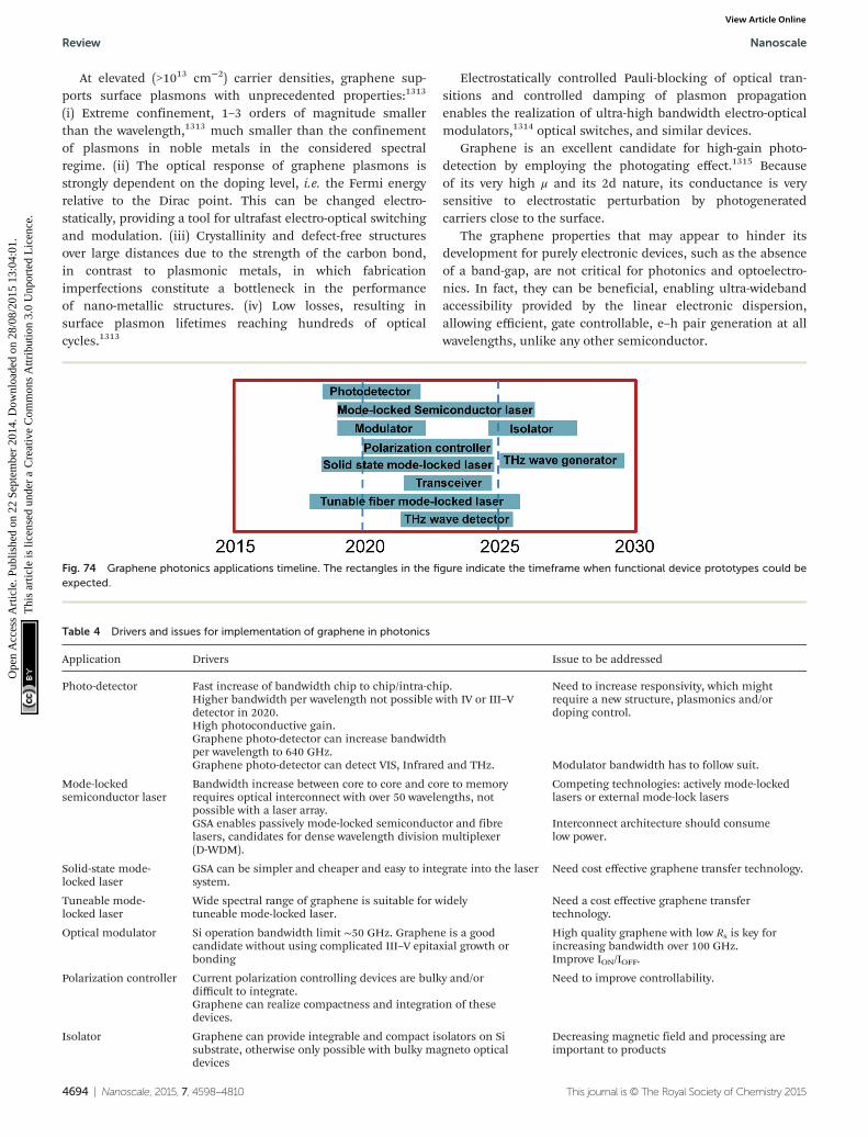
At elevated (>1013 cm−2) carrier densities, graphene sup-ports surface plasmons with unprecedented properties:1313
(i) Extreme confinement, 1–3 orders of magnitude smallerthan the wavelength,1313 much smaller than the confinementof plasmons in noble metals in the considered spectralregime. (ii) The optical response of graphene plasmons isstrongly dependent on the doping level, i.e. the Fermi energyrelative to the Dirac point. This can be changed electro-statically, providing a tool for ultrafast electro-optical switchingand modulation. (iii) Crystallinity and defect-free structuresover large distances due to the strength of the carbon bond,in contrast to plasmonic metals, in which fabricationimperfections constitute a bottleneck in the performanceof nano-metallic structures. (iv) Low losses, resulting insurface plasmon lifetimes reaching hundreds of opticalcycles.1313
Electrostatically controlled Pauli-blocking of optical tran-sitions and controlled damping of plasmon propagationenables the realization of ultra-high bandwidth electro-opticalmodulators,1314 optical switches, and similar devices.
Graphene is an excellent candidate for high-gain photo-detection by employing the photogating effect.1315 Becauseof its very high μ and its 2d nature, its conductance is verysensitive to electrostatic perturbation by photogeneratedcarriers close to the surface.
The graphene properties that may appear to hinder itsdevelopment for purely electronic devices, such as the absenceof a band-gap, are not critical for photonics and optoelectro-nics. In fact, they can be beneficial, enabling ultra-widebandaccessibility provided by the linear electronic dispersion,allowing efficient, gate controllable, e–h pair generation at allwavelengths, unlike any other semiconductor.
Fig. 74 Graphene photonics applications timeline. The rectangles in the figure indicate the timeframe when functional device prototypes could beexpected.
Table 4 Drivers and issues for implementation of graphene in photonics
Application Drivers Issue to be addressed
Photo-detector Fast increase of bandwidth chip to chip/intra-chip. Need to increase responsivity, which mightrequire a new structure, plasmonics and/ordoping control.
Higher bandwidth per wavelength not possible with IV or III–Vdetector in 2020.High photoconductive gain.Graphene photo-detector can increase bandwidthper wavelength to 640 GHz.Graphene photo-detector can detect VIS, Infrared and THz. Modulator bandwidth has to follow suit.
Mode-lockedsemiconductor laser
Bandwidth increase between core to core and core to memoryrequires optical interconnect with over 50 wavelengths, notpossible with a laser array.
Competing technologies: actively mode-lockedlasers or external mode-lock lasers
GSA enables passively mode-locked semiconductor and fibrelasers, candidates for dense wavelength division multiplexer(D-WDM).
Interconnect architecture should consumelow power.
Solid-state mode-locked laser
GSA can be simpler and cheaper and easy to integrate into the lasersystem.
Need cost effective graphene transfer technology.
Tuneable mode-locked laser
Wide spectral range of graphene is suitable for widelytuneable mode-locked laser.
Need a cost effective graphene transfertechnology.
Optical modulator Si operation bandwidth limit ∼50 GHz. Graphene is a goodcandidate without using complicated III–V epitaxial growth orbonding
High quality graphene with low Rs is key forincreasing bandwidth over 100 GHz.Improve ION/IOFF.
Polarization controller Current polarization controlling devices are bulky and/ordifficult to integrate.
Need to improve controllability.
Graphene can realize compactness and integration of thesedevices.
Isolator Graphene can provide integrable and compact isolators on Sisubstrate, otherwise only possible with bulky magneto opticaldevices
Decreasing magnetic field and processing areimportant to products
Review Nanoscale
4694 | Nanoscale, 2015, 7, 4598–4810 This journal is © The Royal Society of Chemistry 2015
Ope
n A
cces
s A
rtic
le. P
ublis
hed
on 2
2 Se
ptem
ber
2014
. Dow
nloa
ded
on 2
8/08
/201
5 13
:04:
01.
Thi
s ar
ticle
is li
cens
ed u
nder
a C
reat
ive
Com
mon
s A
ttrib
utio
n 3.
0 U
npor
ted
Lic
ence
.View Article Online

Based on these unique optoelectronic properties, a widerange of applications can be developed. Here, we summarize aselection of those for which we see technological break-throughs in the near-future:
Highly-integrated graphene photonics. The compatibility ofgraphene with standard CMOS processes at wafer scale makesit a promising candidate for high data-rate (inter- and intra-chip) optical interconnects. Graphene might allow the realiz-ation of high-speed, compact-footprint electro-optical modu-lators, switches and PDs, integrated with Si waveguides orplasmonic circuits. The mechanical flexibility of graphene mayalso enable the integration with bendable substrates andplastic waveguides.
Long-wavelength light detection. Graphene enables lightdetection at wavelengths beyond the current limit set by theband gap of traditional semiconductors, opens up new appli-cations in the FIR (THz) and SWIR and MIR regimes (e.g. bolo-meters and cameras), and has potential for ultrafast pixelateddetection with ballistic transport of generated charge carriers.
Terahertz operation. This will enable products such asportable sensors for remote detection of dangerous agents,environmental monitoring or wireless communication linkswith transmission rates above 100 Gbit s−1.
High-efficiency photodetection. The target is the realizationof highly efficient photocurrent generation by providing a gainmechanism where multiple charge carriers are created fromone incident photon.
Plasmonics and metamaterials. Graphene surface plas-mons as well as tailored metal nanostructures can beexploited to enhance and control the coupling between lightand graphene. This will pave the way to ultra-fast opticalswitching, ultra-strong light-absorption, PVs, and single bio-molecule sensing.
Photonic integrated circuits. The target is to develop activeoptoelectronic devices and co-integrate these with passiveoptical components, such as waveguides,(de-)multiplexers andfilters. Device functionalities comprise the switching androuting of light at ultra-fast speeds and at nano-scale dimen-sions, converting broadband incident light into detectableelectrical signals.
Lasers. Exploiting the broadband saturable absorption pro-perties of graphene, the aim is to realize mode-locked lasers
(e.g., fiber, semiconductor, waveguide and solid state lasers)with broad tunability and bandwidth in the telecommunica-tions and mid-IR range, compared to existing technologies.
The vision is to establish a new field of GRM photonics,sustained by the convergence and co-integration of GRM-based electronic and photonic components such as lasers,optical waveguides, cavities, modulators, photodetectors, andsolar cells.
GRMs may be employed as active optoelectronic materialsto achieve light–matter interaction, convert incident lightenergy into detectable electrical signals, and, vice versa, electri-cal signals may be used to modulate light and realize opticalswitches. For this purpose, GRMs should be integrated withestablished and mature technologies, such as dielectric (Si orplastic) waveguides, optical antennas, plasmonic structures(e.g. gratings or nanoparticles), metamaterials, QDs, etc.Graphene’s constant optical absorption over a spectral rangecovering the THz to the UV allows light detection over a wave-length range superior to any other material. Combined with itshigh μ and Fermi velocity, this implies that devices operatingin the hundreds of GHz range are feasible.
Despite graphene’s absorption of 2.3% being large once itsmonoatomic thickness is considered, it is still necessary toincrease this value to allow more efficient light–matter inter-action and realize highly efficient optoelectronic devices. Forthis purpose, several routes can be pursued. One is the combi-nation of graphene with plasmonic nanostructures,446 wherebythe near-field enhancement due to localized surface plasmonscan significantly increase the light absorption.446 In principle,structures can be designed to achieve 100% light absorp-tion.446 Semiconducting nanoparticles of various shapes andforms can also be used to improve the quantum efficiency.1315
Light harvesting and concentration with these nanostructuresinto graphene leads to increased absorption and moreefficient conversion of light into electrical signals, with anincrease of quantum efficiency.
Another concept involves the integration of graphene withhighly confined optical waveguides, such as Si-on-insulator(SOI) waveguides, widely used in highly-integrated Si photo-nics. As light propagates along the waveguide, it is absorbedalong the length of the propagation and 100% light absorptionmight be possible.1316–1318 Graphene may also be insertedbetween two mirrors to form microcavity-integrated opto-electronic devices.1319 The incident light is reflected by thetop and bottom mirrors and passes through the graphene mul-tiple times. At the resonance condition, constructive interfer-ence enhances the optical field in the cavity, leading toenhanced light–matter interaction and strong opticalabsorption.
The exploitation of plasmons in graphene itself is raisinginterest.252,266,273,1320–1326 The resulting strong light–matterinteraction can be further utilized to enhance detector per-formance as well as to enable radically new light sensingconcepts.
The ever increasing demand for higher-bandwidth bringsalong the need for higher-bandwidth devices on the transmit-
Fig. 75 Schematics of (a) wavelength-independent absorption, (b)broadband photodetection, (c) plasmon generation by a molecule orthrough a plasmon resonance.
Nanoscale Review
This journal is © The Royal Society of Chemistry 2015 Nanoscale, 2015, 7, 4598–4810 | 4695
Ope
n A
cces
s A
rtic
le. P
ublis
hed
on 2
2 Se
ptem
ber
2014
. Dow
nloa
ded
on 2
8/08
/201
5 13
:04:
01.
Thi
s ar
ticle
is li
cens
ed u
nder
a C
reat
ive
Com
mon
s A
ttrib
utio
n 3.
0 U
npor
ted
Lic
ence
.View Article Online
ting, as well as the receiving side, of the communications link.As large parts of the internet traffic are already transmittedoptically, the need for high-speed modulators and photo-detectors in the telecommunications wavelength range(1.3–1.55 μm) is ever more pressing. Moreover, optical inter-connects are currently being introduced as a way to linkcomputers to mobile devices, as well as ultra-high bandwidthlinks for inter- and even intra-chip communication. It wasdemonstrated that graphene photodetectors are capable ofsupporting bandwidths up to 262 GHz,1327 a huge value,but still far below the intrinsic limit, thus far estimated in theTHz range.1328 The speed limit of graphene-based PDs needsto be established. Devices need to be optimized in termsof responsivity, by enhancement with plasmonics andquantum structures, as well as integrated into opticalcavities and waveguides. Electro-optical modulators need to berealized and benchmarked in terms of speed and otherparameters.
The FIR (THz) and MIR regions are fairly unexploited partsof the electromagnetic spectrum, and especially light detectionis difficult as the THz photon energy is below the thermalenergy. However, many interesting applications can bethought of, due to the non-ionizing and low-energy character-istics of THz and MIR radiation. Ranging from medical appli-cations, such as cancer diagnostics, to security, such asexplosive detection, since all materials have characteristic fin-gerprints in the THz/MIR region, a very wide application rangeis feasible. Further, active devices working in the THz/MIRrange are crucial to convert very high frequency signals (in par-ticular, the THz/MIR part of the solar radiation spectrum) intoDC voltage – a feature which could eventually lead to self-powered devices. Having zero-band gap, graphene offers hugepotential to outperform all available semiconductor techno-logies in the THz and MIR range, to reach THz operation fre-quencies, and to enable future wireless THz systems.
Graphene-based sensing and imaging in the SWIR isanother interesting area that lies at the heart of safety andsecurity applications in civil and military surveillance, nightvision applications, automotive vision systems for driver safety,food and pharmaceutical inspection and environmental moni-toring, just to name a few. The SWIR region is so far based onthe use of III–V single crystalline semiconductors for sensing.Imaging has curtailed their monolithic integration to CMOSread-out integrated circuits (ROIC) and focal plane arrays(FPAs).1329 This results in SWIR imaging sensors at a 3-order-of-magnitude greater cost compared to visible-wavelength Si-based ones,1330 and pixel resolution limited to ∼1 MP (megapixel) range,1330 as opposed to tens of MPs offered by currentCMOS imaging sensors.
The 2d nature of graphene makes it also feasible to useCMOS-compatible processing techniques with CVD grownlarge-area graphene, in order to achieve highly-integratedarrays consisting of numerous individual devices. This mayallow the fabrication of pixelated graphene-based camerasworking over an ultra-wide spectral range, enabling imagecapture from the visible to the more unexplored THz/MIR
range. Potential application areas include medical, automotiveand security, such as tissue imaging, driver supporting head-up displays, and explosive/biological species detection.
Current solar cell technologies use only a rather small partof the solar spectrum due to their intrinsic band gap limitingthe maximum detectable wavelength.1331 The absence of aband-gap in graphene translates into the absence of thismaximum detectable wavelength limit and, combined with itsconstant absorption, solar energy over a much wider spectrallength might be converted to electricity. Solar cells based ongraphene, as well as combined with plasmonic and quantumnanostructures, thus need to be explored.
Graphene can be combined with other nanostructures,taking advantage of the strong light absorption in QDs and the2-dimensionality and high μ, to merge these materials into ahybrid system for photodetection with high sensitivity.1315
Further, the integration with plasmonic metamaterials willenable a new class of optical switches for displays.
Surface enhanced Raman Spectroscopy (SERS) can in prin-ciple achieve signal enhancements of up to 1015.1332 Plasmonicnanostructures enhanced sensing may lead to detection limitson the single-molecule level. The near-field enhancementresulting from the combination of graphene with plasmonicnanostructures1333 will increase the signal sufficiently.1334
Such structures will also benefit from graphene’s compatibilitywith biological species. Combined with graphene’s single-elec-tron charge sensitivity, we expect this technology to become anew platform for medical applications, not only providingenhancement at the single-molecule sensing level, but alsobeing bio-compatible.
Integration of graphene into a cheap, flexible sensing plat-form based on plastics must be explored. It is envisaged tointegrate and merge the aforementioned medical and THz/MIR sensors with plastic electronics to achieve a sensing-plat-form for wearable electronics, as well as low-cost one-time usesensors for use in developing countries.
7.1. Graphene saturable absorbers and related devices
Materials with nonlinear optical and electro-optical propertiesare needed in most photonic applications. Laser sources pro-ducing nano- to sub-ps pulses are key components in the port-folio of leading laser manufacturers. Regardless of wavelength,the majority of ultrafast laser systems use a mode-locking tech-nique, where a nonlinear optical element, called a saturableabsorber (SA), turns the continuous-wave output into a train ofultrafast optical pulses.1335 The key requirements are fastresponse time, strong nonlinearity, broad wavelength range,low optical losses, high power handling, low power consump-tion, low cost and ease of integration into an optical system.Currently, the dominant technology is based on semiconduc-tor SA mirrors (SESAMs).1335,1336 However, these have a narrowtuning range, and require complex fabrication and packa-ging.1335,1353 The linear dispersion of the Dirac electrons ingraphene offers an ideal solution: for any excitation there isalways an e–h pair in resonance. The ultrafast carrierdynamics512,513,1337,1338 combined with large absorption171,990
Review Nanoscale
4696 | Nanoscale, 2015, 7, 4598–4810 This journal is © The Royal Society of Chemistry 2015
Ope
n A
cces
s A
rtic
le. P
ublis
hed
on 2
2 Se
ptem
ber
2014
. Dow
nloa
ded
on 2
8/08
/201
5 13
:04:
01.
Thi
s ar
ticle
is li
cens
ed u
nder
a C
reat
ive
Com
mon
s A
ttrib
utio
n 3.
0 U
npor
ted
Lic
ence
.View Article Online

and Pauli blocking, make graphene an ideal ultrabroadband,fast SA.1339,1353 Unlike SESAMs and CNTs,1340–1352 graphenedoes not require bandgap engineering or chirality/diametercontrol.1339,1353
Since the first demonstration in 20091353 (Fig. 76), the per-formance of ultrafast lasers mode-locked by graphene hasimproved significantly. E.g., the average output power hasincreased from a few mW1353 to over 1 W.1354
LPE1339,1353,1355–1359 CVD,1360,1361 carbon segregation,1362
MC1359,1363 have been used for graphene saturable absorber(GSA) fabrication. So far, GSAs have been demonstrated forpulse generation at 1,1369 1.2,1370 1.51339,1353,1360,1363,1366 and2 µm.1364 The most common wavelength is ∼1.5 μm, not dueto GSAs wavelength restriction, but because this is the stan-dard wavelength of optical telecommunications. Ref. 1356reported a widely tuneable fiber laser mode-locked with a GSA.The laser produces ps pulses in a tuning range 1525–1559 nm,demonstrating its “full-band” operation performance.
Fiber lasers are attractive due to their efficient heat dissipa-tion and alignment-free format.1365 GSAs have been used tomode-lock fiber lasers.1339,1353,1355–1357,1360,1363,1366 For fiberlasers, the simplest and most economical approach for GSAintegration relies in sandwiching directly the GSA between twofiber connectors (Fig. 76) [see ref. 1356, 1360, 1363, 1366 and1339]. Other options (e.g. evanescent-wave based inte-gration1367) have also been demonstrated for high-power gene-ration. Sub-200 fs pulses were achieved using a stretched-pulsedesign, where the cavity dispersion is balanced to stretch thepulse for the limitation of nonlinear effects.1355
Solid-state lasers are typically used for high-power output,as alternative to fiber lasers.1368 GSAs have also been demon-strated to mode-lock solid-state lasers.1369–1372 In this case,CVD graphene (>1 cm2) was directly transferred to a quartzsubstrate.1370 Ref. 1370 reported 94 fs pulses with 230 mWoutput power. Another approach for GSA fabrication relies inspin-coating LPE graphene either on quartz or high-reflectivitymirrors. GSA can then be inserted into a solid-state cavity. Thiswas used to achieve average power up to 1 W using a solid-state Nd:YVO4 laser,1372 with ∼1 µm output wavelength and∼14 nJ energy.
SLG grown via CVD was also used in ultrafast vertical-external-cavity surface-emitting lasers (VECSELs).1361 AVECSELconsists of an external cavity, formed by high-reflectionmirrors, and an output coupler, with typical cavity lengths of afew mm up to tens of cm.1335,1373 The gain chip generally con-tains a highly reflective bottom section to reflect the laser andpump light, an active semiconductor gain section, and an anti-reflective top layer.1335,1373,1374 VECSELs combine the advan-tages of semiconductor lasers, such as compact footprint(down to ∼3 mm cavity1375), with those of diode pumped solid-state lasers, such as low timing jitter,1376 excellent beamquality,1377 high average1377 and peak power1378,1379 VECSELsare mode-locked by SESAMs, epitaxially grown on lattice-matched semiconductor substrates.1335 However, SESAMs onlyoffer a limited operation bandwidth (to date, the broadesttuning range of VECSELs mode-locked with SESAMs is13.7 nm1380). Ref. 1361 controlled the electric field intensity inSLG by changing its absorption on a high-reflection mirror.The resulting SLG-based saturable absorber mirrors (GSAMs)have shown an unsaturated loss adjustable from 0 up to 10%and modulation depth up to 5%.1361 These enabled to mode-lock a VECSEL with a series of different gain chips over a46 nm wavelength range (from 935 to 981 nm) with repetitionrates up to 2.48 GHz, and 466 fs pulse duration. These resultscan lead to novel graphene-based ultrafast light sources tomeet the wavelength range, repetition rate and pulse durationrequirements for various applications (e.g. metrology, spectro-scopy and data-communication).
Graphene is also promising for other photonic applications,such as optical limiters1381 and optical frequency conver-ters.1381 Optical limiters are devices that have high transmit-tance for low incident light intensity and low transmittance forhigh intensity. There is a great interest in these for opticalsensors and human eye protection,1381 as retinal damage canoccur when intensities exceed a certain threshold.1381 Passiveoptical limiters, which use a nonlinear optical material, havethe potential to be simple, compact and cheap.1381 However,so far no passive optical limiters have been able to protect eyesand other common sensors over the entire visible and NIRrange.1381 Typical materials include semiconductors (e.g. ZnSe,InSb), organic molecules (e.g. phthalocyanines), liquid crystalsand carbon-based materials (e.g. carbon-black dispersions,CNTs and fullerenes).1382 In graphene-based optical limitersthe absorbed light energy converts into heat, creating bubblesand microplasmas,1382 which results in reduced transmission.Graphene dispersions can be used as wideband optical limit-ers covering visible and NIR. Broad optical limiting (at 532 and1064 nm) by LPE graphene was reported for ns pulses.1382 Ref.1383 reported that FG dispersions could outperform C60 as anoptical limiter.
Optical frequency converters are used to expand the wave-length accessibility of lasers (e.g., frequency doubling,parametric amplification and oscillation, and four-wavemixing).1381 Calculations suggest that nonlinear frequencygeneration in graphene (e.g. harmonics of input light) shouldbe possible for sufficiently high external electric fields (>100 V
Fig. 76 Graphene fiber laser.1353 WDM, wavelength division multi-plexer; PC, polarization controller; EDF, erbium-doped fiber; ISO,isolator.995
Nanoscale Review
This journal is © The Royal Society of Chemistry 2015 Nanoscale, 2015, 7, 4598–4810 | 4697
Ope
n A
cces
s A
rtic
le. P
ublis
hed
on 2
2 Se
ptem
ber
2014
. Dow
nloa
ded
on 2
8/08
/201
5 13
:04:
01.
Thi
s ar
ticle
is li
cens
ed u
nder
a C
reat
ive
Com
mon
s A
ttrib
utio
n 3.
0 U
npor
ted
Lic
ence
.View Article Online

cm−1).1384 Second-harmonic generation from a 150 fs laser at800 nm was reported.1385 In addition, four-wave mixing togenerate NIR tunable light was demonstrated using SLG andFLG.1386 Graphene’s third-order susceptibility |χ3| wasmeasured to be ∼10−7 e.s.u.,1386 up to one order of magnitudelarger than CNTs.1386 Other features of graphene, such as thepossibility of tuning the nonlinearity by changing N, and wave-length-independent nonlinear susceptibility1386 could be usedfor various photonic applications (e.g. optical imaging).
The main parameters of a pulsed laser are output power (orsingle pulse energy), output spectral coverage (e.g. operationwavelength, wavelength tuneability), pulse duration and rep-etition rate. The requirements for ultrafast laser are highlyapplication-dependent. E.g., for fiber-optical communications,the operation wavelength is ∼1.5 μm as optical fibers have lowloss and low dispersion around this spectral range.1387 Formedical applications (e.g. laser surgery), the required laseroperation wavelengths mainly depend on the peak absorptionof different tissues.1388,1389 These range from MIR for mini-mally invasive surgery of skin cutting,1390 to UV for athermalphotoablation.1391 For high-speed fiber-optical signal trans-mission and processing, high-repetition rate (>GHz) allows thesignal to carry more data, while for industrial material proces-sing (e.g. micro-machining), kHz pulses are commonly usedto decrease the cumulative heating caused by multiple laserpulses.1392 In general, high output power, wide spectral cover-age, short pulse width, and high repetition rate are desirable,because it is easy to reduce the output power (e.g. by attenua-tors), narrow the spectral coverage (e.g. by optical filters),broaden the pulse duration (e.g. by dispersive fibers) anddecrease the repetition rate (e.g. by optical choppers), butnot vice-versa. Furthermore, stability, cost, compactnessand efficiency (e.g. electrical-to-optical or optical-to-opticalefficiency) also are key for applications.
7.1.1. 2d crystals-based saturable absorbers. Other 2d crys-tals (i.e. MoS2, Bi2Te3, Bi2Se3) have shown ultrafast carrierdynamics.1393–1401 Driven by the development of GSA, recently2d crystals such Bi2Te3,
1402,1403 Bi2Se3,1404–1406 Sb2Te3,
1407
MoS21408 have been used as SA for ultrafast pulse generation.
Tunable output results have been demonstrated.28 Thus far,2d crystals-based ultrafast lasers only have been demonstratedon erbium-doped fiber lasers (EDFLs)1402,1404–1407 andthulium/holmium co-doped fiber laser.1403 However, it isexpected that other 2d crystals will soon be employed on otherlasers (e.g., ytterbium-doped fiber lasers – YDFL-, thulium-doped fiber lasers TDFL and solid-state and waveguide lasersas well).1058
Ref. 1409 reported resonant nonlinear optical suscepti-bilities at the edges of MoS2 flakes, allowing direct opticalimaging of the atomic edges and boundaries of such 2dcrystal. Indeed, the structural discontinuity at the edges andboundaries of 2d crystals, e.g., graphene and TMDs, leads tocomplex interplay between the atomic positions and the elec-tronic structures.1409 Subsequently, the atomic edges andboundaries reconstruct structurally and electronically due tothe translational symmetry breaking.1409 Ref. 1409 developed a
nonlinear optical imaging technique that allows rapid and all-optical determination of the crystal orientations of the MoS2 ata large scale. Moreover, zigzag nanoribbons showed a two-photon resonance at ∼0.8 eV, originating from the subbandtransitions from the valence bands to the isolated edge statesof the Mo-zigzag edges.1409 These results pave the way for theexploitation of other 2d crystals and their use as sub-band gapSA. In view of large scale integration, 2d crystals produced byLPE,35,250,602,624,625,629 that can maximize edges250,622 duringthe ultracentrifugation process, could be an useful route tocreate these novel SAs.
7.1.2. Output power/pulse energy. Currently, solid-statelasers and fiber lasers are the most commonly used for highoutput power/pulse energy applications, mainly because theyallow high-power pump.1368 Solid-state lasers are advantageousin terms of high pulse energy and peak power, as fiber laserssuffer from nonlinear effects. E.g., Watt-level ultrafast Ti:sap-phire lasers and their low-repetition-rate (<kHz), high energyand high peak power amplifiers are widely used for academicresearch. The primary limitation of solid-state lasers to achievehigh average power is thermo-optic effects,1410 such as thermallensing.1411 Compared to solid-state rod and slab lasers, solid-state thin-disk designs significantly reduce thermal effects andnonlinearities, due to the pump configuration and small thick-ness (∼a few hundred μm) of the gain medium. This could bea solution to high average power and high energy pulses. GSAscould be used in thin-disk designs for this purpose. The mainchallenge is the large non-saturable loss of these SAs, whichcan be addressed by further devices.
Compared to solid-state laser, fiber lasers have a greaterpotential for high average power because of their better heatdissipation,1412 due to large surface- to-volume ratio. However,the nonlinear effects, enhanced by strong mode confinementand the long fiber required (∼10 m)1365, may distort thepulses, and restrain the maximum peak power. Large-mode-area fiber (e.g. photonic crystal fiber, PCF) based ultrafastlasers working in a dissipative solution regime have beendemonstrated1413 for high average power ultrafast pulse gene-ration with MW peak power (e.g. 11 W average power and 1.9MW peak power from a SESAM mode-locked Yb-doped PCFlaser1413). In principle, large-mode-area fiber lasers mode-locked with GSA may deliver better performances (e.g. higheraverage power, higher peak power, system simplicity). E.g.,coating GSAs on the fiber surfaces to achieve evanescent-waveinteraction can preserve the alignment-free waveguide formatby removing the free-space components, necessary for tra-ditional SA coupling. It is also possible to put GSAs inside thefiber (e.g. holes of PCFs). These integration strategies (i.e. gra-phene on the surfaces or inside the devices) can be applied tovarious lasers: waveguide (e.g. laser inscribed waveguide andpolymer waveguide) and semiconductor (e.g. VECSELs andoptically pumped semiconductor disk lasers) for high power/energy pulse generation.
For applications it is not necessary to generate high averagepower ultrafast output only using one oscillator, as externalcavity processing can increase the output power. E.g., external
Review Nanoscale
4698 | Nanoscale, 2015, 7, 4598–4810 This journal is © The Royal Society of Chemistry 2015
Ope
n A
cces
s A
rtic
le. P
ublis
hed
on 2
2 Se
ptem
ber
2014
. Dow
nloa
ded
on 2
8/08
/201
5 13
:04:
01.
Thi
s ar
ticle
is li
cens
ed u
nder
a C
reat
ive
Com
mon
s A
ttrib
utio
n 3.
0 U
npor
ted
Lic
ence
.View Article Online

amplification of graphene mode-locked lasers or coherentcombination of various lasers could boost output power andenergy.
7.1.3. Spectral coverage. The operation wavelength is animportant parameter. In particular, a range of applications(e.g. ultrafast PL) require resonant excitation, thus ultrafastlasers covering a broad wavelength range are attractive. Wave-length tunable1346 or switchable lasers are another solution toaccess a broadband spectral range. Combination of wide-bandgain materials (e.g. Ti:sapphire) and GSAs could provide novelbroadband tuneable ultrafast sources to meet the requirementfor a wideband range.
The output wavelength or tuning spectral range of a tra-ditional laser will be ultimately constrained by the gainmedium. E.g., Ti:sapphire typically only works between 0.65and 1.1 μm.1414 Nonlinear effects (e.g. optical parametric gene-ration and Raman scattering) can be used to broaden the spec-tral range. They can provide gain covering from UV to THz.
Nonlinear frequency conversion (e.g. harmonic frequencygeneration, parametric oscillation and amplification, four-wave mixing, supercontinuum generation) is also useful toexpand the wavelength accessibility after the oscillator.
7.1.4. Pulse width. Shorter optical pulses can providebetter temporal resolution and high-speeds (e.g. pulse widthsof 200–400 fs can enable 1.28 TB s−1 optical communi-cations1415). In general, solid-state lasers facilitate shorterpulse generation (e.g. 4.4-fs pulses from a Ti:sapphire laseroscillator1416), as the shortest pulse that fiber lasers can gene-rate is typically limited by enhanced nonlinearity.1416 Indeed,so far, the shortest pulse duration for GSAs (94 fs from a Cr:forsterite laser1417) was achieved with solid-state lasers.1418
These could be shortened further by using broadband solid-state gain materials (e.g. Ti:sapphire). E.g., with wideband gainmedia and laser design optimization (e.g. dispersion manage-ment), graphene mode-locked lasers could generate pulses asshort as those produced by any other SAs, but with reducedsystem complexity. One of the limitations to get shorter pulsesis the medium narrow gain bandwidth. Nonlinear effect-basedgain has much broader bandwidth, which also supports ultra-fast pulse generation. E.g., the combination of broadbandRaman gain and GSAs can enable shorter pulse duration thanever before.
External-cavity methods (e.g. nonlinear compression, orcoherent combining) could also be used to generate shorterpulse down to a few optical cycles (a cycle is defined as thetime needed for light to travel over a distance equal to thelight wavelength) (e.g. 4.3-fs).1355
7.1.5. Repetition rate. The repetition rate is inversely deter-mined by the cavity length.1335 This means that shorter cavitiespermit higher repetition rates, and vice versa. Pulsed lasingwith short cavities generally requires high-gain materials, alow-loss cavity, and low-loss SAs. So far, multi-GHz pulsesources have been demonstrated for mode-locked semiconduc-tor lasers (e.g. 50 GHz from a 3 mm SESAM mode-locked semi-conductor laser1419), and compact solid-state lasers (e.g. 157GHz from a 440 μm Nd:YVO4 laser mode-locked with
SESAMs1420). Waveguide lasers also allow high repetition rate(e.g. ∼400 MHz). GSAs have low non-saturable losses, whichmakes them suitable for short cavity lasers. Coating grapheneon surfaces/facets of the cavity components (e.g. fiber, wave-guide, semiconductor, monolithic solid-state materials, ormirrors) could enable compact lasers with repetition rates upto hundreds of GHz.
Another option to push the output repetition rate is toexploit harmonic mode-locking.1421 This requires a complexdesign to achieve precisely equidistant pulses, as the fluctu-ations of the temporal positions of pulses from those in a per-fectly periodic pulse train (also termed timing jitter1422) isdetrimental for various applications, such as fiber-optic com-munication and optical sampling measurements.
7.1.6. Other considerations. Solid-state lasers are superiorto other lasers for high pulse quality (e.g. smooth spectralprofile and low chirp) ultrafast pulse generation, since otherwaveguide formats (e.g. fiber lasers) are subject to dispersionand enhanced nonlinear effects and have low pulse quality(e.g. spectral side-bands, high chirp, increasing or decreasingtotal pulse dispersion with signal propagation). Waveguide-based ultrafast lasers also suffer from birefringence.1423,1424
This leads to challenges in applications where polarizationmode dispersion or birefringence splitting is critical for thedesired responses from optical devices.1425 Birefringence canbe eliminated by using polarization-maintaining fibers. Unfor-tunately, nonlinear polarization evolution based mode-locking(i.e. mode-locking using optical intensity dependent polariz-ation direction rotation1426) cannot be applied to polarization-maintaining fibers (PMF), as the polarization in PMFs doesnot change with optical intensity. GSAs have potential forpolarization-maintaining fiber lasers.
Fiber lasers and other alignment-free waveguide basedlasers can offer excellent beam quality even when operated athigh average power, because of reduced thermal effects.1427 Inaddition, they are compatible with fiber delivery, which offersflexibility in system design and use. In terms of fabricationcost, it is also inexpensive to fabricate fiber lasers to meetapplications with low demand on pulse energy (∼1 nJ), polariz-ation, emission bandwidth, pulse quality, etc., as most fiberdevices are economically available due to their mass-pro-duction for fiber-optical communications. GSAs are interestingfor this type of fiber lasers, as they can further decrease thefabrication costs and reduce system complexity compared totraditional SA technologies (e.g. SESAMs).
In order to increase the damage threshold, graphene-basedoptical limiters need to be developed on two fronts. The first isto grow on-demand graphene with the desired characteristics,while the other is to design new optical geometries that maxi-mize the range of protection. E.g., the use of two focal planesoffers new possibilities for the optimization of graphene-basedoptical limiting.
The aim will also be to enhance the frequency conversioneffect. Graphene samples as large as tens of cm for ICT appli-cations and as small as a few mm for microchip laser appli-cations need to be routinely produced. The combination of
Nanoscale Review
This journal is © The Royal Society of Chemistry 2015 Nanoscale, 2015, 7, 4598–4810 | 4699
Ope
n A
cces
s A
rtic
le. P
ublis
hed
on 2
2 Se
ptem
ber
2014
. Dow
nloa
ded
on 2
8/08
/201
5 13
:04:
01.
Thi
s ar
ticle
is li
cens
ed u
nder
a C
reat
ive
Com
mon
s A
ttrib
utio
n 3.
0 U
npor
ted
Lic
ence
.View Article Online

growth capabilities, device design and assembly, is expected toresult in products with superior performance.
7.2. Photodetectors
PDs measure photon flux or optical power by converting theabsorbed photon energy into electrical current. They arewidely used in a range of devices,1428 such as remote controls,televisions and DVD players. Most exploit the internal photo-effect,1429,1430 in which the absorption of photons results incarriers excited from the valence to the conduction band, out-putting an electric current. The spectral bandwidth is typicallylimited by the absorption.1428 Graphene absorbs from the UVto THz.1431,1432 As a result, graphene-based photodetectors(GPD), see Fig. 77, could work over a much broader wavelengthrange.
The response time is ruled by μ. Graphene has huge μ, so itcan be ultrafast.1428 Graphene’s suitability for high-speed PDswas demonstrated in a communications link at 10 Gbit s−1
(ref. 1433).In this section we summarize some key concepts as dis-
cussed in ref. 1434.Many of the characteristics and unique capabilities of
photodetection systems based on GRMs have been studiedover the past few years, and a multitude of application areashave been addressed. Some of these have already reached alevel of competitiveness with existing technologies. Variousphotodetection schemes and architectures have been proposedto date. The simplest configuration is the metal–graphene–metal (MGM) PD in which graphene is contacted with metalelectrodes as source and drain.1429,1435,1436 Further, these PDscan be enhanced with plasmonic metal nanostructures,446
intrinsic plasmons,1437 p–n junctions in the graphenechannel,1438,1439 and integration with waveguides,1318,1440,1441
and microcavities.1319,1442 Hybrid approaches employ semi-conducting nano-particles, molecules, or plasmonic nano-systems as light absorbing materials, with graphene as the con-duction channel, resulting in photoconductive-gain.1315,1443,1444
Devices have also been fabricated for detection of THz light,1445
where an antenna coupled to source and gate of the deviceexcites plasma waves in the channel. Most importantly,graphene is compatible with the highly mature Si-based plat-form for electronics and photonics, making it a strong conten-
der for low-cost and large-scale integration into optoelectronicnetworks and multi-pixel CMOS read-out circuits.
7.2.1. Figures of merit. Light impinging on a device, witha photon energy Eph and power Pin, corresponds to an incom-ing photon flux ϕin = Pin/Eph [s−1], and an absorbed photonflux ϕabs = ϕin·Aabs [s−1], with Aabs the absorbed fraction. Theexternal quantum efficiency (EQE) is equal to the number ofe–h pairs per second collected to produce the photocurrent Iph[C s−1], divided by the number of incident photons persecond: EQE = (Iph/q)/ϕin, with q the electron charge. Theinternal quantum efficiency (IQE) is calculated in a similar wayexcept that in this case the absorbed photon flux is con-sidered: IQE = (Iph/q)/ϕabs. The responsivity of a PD is thephotocurrent Iph divided by the incident power: Rph = Iph/Pin[AW−1; can also be given in V W−1 in the case of photovoltage],or in case the photo-induced voltage Vph is measured: Rv = Vph/Pin. E.g., in a PD with 100% EQE, Rph = 1 A W−1 for Eph = 1 eV.One figure of merit conventionally employed to compare mmand sub-mm detector performances is the noise equivalentpower (NEP) [W Hz−1/2].1446 This is a function of noise andresponsivity and is defined as the value of the root meansquare (rms) input radiant signal power required to producean rms output signal which is equal to a rms noise value witha signal to noise ratio of 1, usually expressed in units W per√Hz. Another typical figure of merit used to characterize theperformance of a detector is the specific detectivity D* [cmHz1/2 W−1, this unit is named after R. C. Jones, whereby 1 cmHz1/2 W−1 = 1 Jones, in recognition of his work on sensitivityof radiation sensors1447], which is given by D* ¼ ffiffiffiffiffiffiffiffiffiffiffiffiffiffi
A � BWp=NEP.
Here, A is the area of the photosensitive region, and BW is thefrequency bandwidth of the detector. For sensitized photo-conductors the external quantum efficiency is defined as QE =ηtransηabs, where ηtrans is the charge transfer efficiency and ηabsis the light absorption efficiency. A second important par-ameter is the lifetime, τtr, of the charge residing in the par-ticles, as the light-induced change in carrier density Δn scaleslinearly with it: Δn = τtr × QE × ϕin. Photoconductive detectorsare often benchmarked by their photoconductive gain, Gph =(Iph/q)/(ϕinQE), i.e. the number of detected charge carriers persingle incident photon. This can be quantified by the ratio ofthe lifetime of the trapped carriers over the drift transit time,τtransit, of the SLG charge carriers from source to drain: Gph =τtr/τtransit. τtransit is governed by the applied field, thus it isshorter for higher bias and mobility: τtransit = L2/(μVbias), with Lthe source–drain separation distance.
7.2.2. Physical mechanisms enabling photodetection. Theconversion of absorbed photons into an electrical signal is thephysical principle on which photodetection and other opto-electronic applications are based on. Photovoltaic (Fig. 78a),photo-thermoelectric (Fig. 78b), bolometric (Fig. 78c), andphotogating effects, together with the Dyakonov–Shur (DS)(Fig. 78d) or plasma-wave-assisted mechanism are the mecha-nisms by which photodetection can be accomplished in gra-phene, see Fig. 78. Here we briefly discuss these mechanisms.
7.2.2.1. Photovoltaic effect. The photovoltaic photocurrentgeneration is based on the separation of photo-generated e–hFig. 77 Scheme of a MGM photodetector. Adapted from ref. 995.
Review Nanoscale
4700 | Nanoscale, 2015, 7, 4598–4810 This journal is © The Royal Society of Chemistry 2015
Ope
n A
cces
s A
rtic
le. P
ublis
hed
on 2
2 Se
ptem
ber
2014
. Dow
nloa
ded
on 2
8/08
/201
5 13
:04:
01.
Thi
s ar
ticle
is li
cens
ed u
nder
a C
reat
ive
Com
mon
s A
ttrib
utio
n 3.
0 U
npor
ted
Lic
ence
.View Article Online

pairs by built-in electric fields at junctions between negatively(n-type) and positively (p-type) doped regions of graphene orbetween differently-doped sections in general1430,1448,1449
(Fig. 78a). The same effect can be achieved by applying asource-drain bias voltage, producing an external electric field.However, this is generally avoided in the case of graphene, asit is a semi-metal, therefore generating a large dark current.
The doping that generates the built-in field can be intro-duced either by local chemical doping,1166 electrostatically, bythe use of two (split) gates,1438,1448 or by taking advantage ofthe work-function difference between graphene and a contact-ing metal.1433,1448–1450 In the case of split gates, the dopingcan be tuned to be p or n, depending on the applied gate vol-tages, while in the case of graphene–metal junctions thedoping in the contacted area is fixed. This is typically p-typefor metals with a work function higher than the work functionof intrinsic graphene (4.45 eV),1451 while the graphene channelcan be p or n. The PV photocurrent direction depends only onthe direction of the electric field, not on the overall dopinglevel. Thus, it switches sign, when going from p–n to n–p, orfrom p–p+ to p+–p, where p+ means stronger p-type dopingcompared to p.
A lower bound on the intrinsic response time of SLG basedMGM PDs was measured using an ultrafast optical correlationtechnique to be about 2 ps.1327 However, while the photogene-rated carriers in graphene can have very high μ, the photode-tection speed is not limited by the transit time of thesecarriers, but by the RC (resistance multiplied by capacitance)characteristics of the detector.23 Both response time and
photo-detection efficiency depend on the ultrafast scatteringprocesses. We note that e–e scattering513,1452,1453 can lead tothe conversion of one high energy e–h pair into multiple e–hpairs of lower energy.512,1453,1454 This process, also denoted ascarrier multiplication, can potentially enhance the overallphoto-detection efficiency. Electron-phonon scatter-ing,134,135,1455,1456 on the other hand, transfers electron energyto the phonons, which may lead to bolometric effects, as dis-cussed in more detail below.
7.2.2.2. Photo-thermoelectric effect. Hot-carrier-assistedtransport can play an important role in graphene1438,1439
(Fig. 78b). Due to the large optical phonon energy scale in thismaterial208,1456 (∼200 meV), hot carriers created by the radi-ation field can remain at a temperature Te (and thus energykBTe) higher than that of the lattice for many ps. Final equili-bration of the hot electrons and the lattice occurs via theslower scattering between charge carriers and acousticphonons.1457,1458 These processes take place on a ns time-scale,1457 although they experience a substantial speed-upattributed to disorder-assisted collisions.1459–1461
The photo-generated hot electrons can produce a photo-voltage VPTE by the photo-thermoelectric (PTE) effect (Seebeckeffect): VPTE = (S2 − S1)ΔTe VPTE = (S2 − S1)ΔT, where S1,2 [V/K]is the thermoelectric power (Seebeck coefficient) in the twographene regions with different doping, and ΔTe is the Tedifference between the regions. More generically, the photo-voltage VPTE can be calculated by integrating the local electricfield which is generated by an optically-generated temperaturegradient, dTe/dx, together with a spatially varying Seebeckcoefficient: EPTE =
ÐS·∇Tdx. The PTE effect has been shown to
dominate in graphene p–n junctions1438,1439 or in suspendedgraphene.1462 Because hot electrons, rather than latticeheating, generate the electronic response under these con-ditions, PTE graphene detectors can achieve high bandwidths,as in the case of PV detectors. The thermoelectric power S(also called thermopower) is related to the electrical conduc-tivity σ by the Mott formula:1463
S ¼ � π2kB2Te
3q1σ
@σ
@ε; ð1Þ
where kB is the Boltzmann constant, q is the electron charge,and the derivative of the electrical conductivity σ with respectto energy ε must be evaluated at the Fermi energy, i.e. at ε = εF= ħνFκF, with νF the Fermi velocity, kF ¼ ffiffiffiffiffiffiffiffi
πjnjpthe Fermi wave
vector, and n the carrier density. The Mott formula was derivedutilizing the Sommerfeld expansion,1463 thus it is valid onlyfor kBT ∝ εF. For this condition, S can be calculated from thetransport characteristics of the device, i.e. from the depen-dence of conductance on gate voltage.
The sensitivity of PDs based on the PTE effect might beenhanced due to efficient intraband e–e scattering, leading tohigher Te.
1464,1465 A typical Rph ∼ 10−3 A W−1 was reported forPTE graphene PDs,31 similar to those of PV graphene PDs.However, higher Rph ∼ 10−2 A W−1, was observed in suspendedTLG p–n junctions.1462 In this case, the interaction of substrate
Fig. 78 Schematic representation of the four different photocurrentgeneration mechanisms, (a) photovoltaic, (b) photothermoelectric, (c)bolometric and (d) plasma wave-assisted (Dyakonov–Shur). Adaptedfrom ref. 1434.
Nanoscale Review
This journal is © The Royal Society of Chemistry 2015 Nanoscale, 2015, 7, 4598–4810 | 4701
Ope
n A
cces
s A
rtic
le. P
ublis
hed
on 2
2 Se
ptem
ber
2014
. Dow
nloa
ded
on 2
8/08
/201
5 13
:04:
01.
Thi
s ar
ticle
is li
cens
ed u
nder
a C
reat
ive
Com
mon
s A
ttrib
utio
n 3.
0 U
npor
ted
Lic
ence
.View Article Online
phonons with graphene electrons is inhibited, removing animportant electron-phonon decay channel. This shows thatelectron/substrate polar phonon scattering can play a role,especially at RT, and removing it by suspending the graphenesheet can increase the hot electron temperature, and thus thephotocurrent.
7.2.2.3. Bolometric effect. The bolometric effect is associ-ated with the change in the transport conductance producedby heating associated with the incident photons (Fig. 78c).A bolometer measures the power of electromagnetic radiationby absorbing the incident radiation (dP) and reading out theresulting temperature increase dT.1446 Today, bolometers aremainly made of semiconductor1466 or superconductor absorp-tive materials,1446 and are widely used in the sub-millimeter(THz) wavelength range, where they are among the most sensi-tive detectors. The key parameters of a bolometer are thethermal resistance Rh = dT/dP, which ultimately defines itssensitivity, and the heat capacity Ch, which determines itsresponse time τ = RhCh.
1446 Graphene has small volume andlow density of states, which results in low heat capacity Ch,thus a fast response. The cooling of electrons by acousticphonons is inefficient, due to the small Fermi surface, andcooling by optical phonons requires very high Te (kBTe > 0.2eV). Thus Rh is high giving rise to high bolometric sensitivity.
As this photodetection mechanism is based on a light-induced change in conductance instead of direct photocurrentgeneration, it requires an externally applied bias and canoperate on homogeneous graphene, without the need to intro-duce a p–n junction. The conductance change induced by theincident light can be due to two mechanisms: (1) a change inthe number of carriers contributing to the current; (2) achange in carrier mobility due to the associated temperaturechange. We note that (1) coincides with the photovoltaiceffect, with the electric field generated by the external bias.
7.2.2.4. Photogating effect. The photogating process isassociated to a light-induced change of the carrier density Δnof a conductor, therefore of its σ. For graphene, this change inσ is given by the relation: Δσ = Δn·e·µ.1434 Typically, the photo-gating effect starts with light absorption inside sensitizingcenters in the vicinity of the GRM, such as nano-particles ormolecules.1434 This absorption process leads to the generationof e–h pairs. Next, one type of charge carrier is transferred tothe GRM (e.g. by an intrinsic electric field) while the other typeof charge carrier resides in the particles, molecules or traps.As long as these charges are trapped, the other type of chargesin the GRM sheet are re-circulated, due to the charge conserva-tion condition. We note that the fundamental difference to thebolometric effect, which is based on the change in μ due toheating, is that the photogating effect is based on a light-induced change in n.
Gph can be strongly enhanced by using a high-µ conductor(such as graphene) and by a long τtr. At the same time, a longτtr reduces the operation speed. Therefore these detectors canbe used for lower temporal bandwidth, such as video imagingapplications. Photoconductive detectors may exhibit a highdark current, so a proper assessment of the detector perform-
ance is not just provided by the responsivity, but rather bymeasuring the NEP or D*.
7.2.2.5. Plasma-wave-assisted mechanism. Dyakonov andShur (DS)1468,1469 proposed a photo-detection scheme, wherebya finite dc voltage is generated in response to an oscillatingradiation field (Fig. 78d). This is based on the fact that a FEThosting a 2d electron gas can act as a cavity for plasmawaves.1470 When these are weakly damped, i.e. when a plasmawave launched at the source can reach the drain in a timeshorter than the momentum relaxation time τ, the detection ofradiation exploits constructive interference of the plasmawaves in the cavity, which results in a resonantly enhancedresponse. This is the so-called resonant regime of plasma-wavephotodetection,1469 and can give rise to a signal that is 5–20times stronger than the broadband non-resonant one. Broad-band detection occurs when plasma waves are overdamped,i.e. when a plasma wave launched at the source decays beforereaching the drain.1469
DS showed1469 that the photovoltage response of a 2d elec-tron system in a FET, i.e. the electric potential differencebetween drain and source, contains a dc component even ifthe incoming field is ac, and thus provides rectification of thesignal. This is particularly useful for the detection of THz radi-ation. Rectification occurs due to the non-linear response ofthe 2d electron gas in the FET channel and is unrelated toextrinsic rectification mechanisms due to e.g. Schottky barriersat contacts or other circuital elements that respond in a non-Ohmic manner. For the resonant regime, the dc photo-response is characterized by peaks at odd multiples of thelowest plasma-wave frequency.1469 Resonant detection of THzradiation in graphene FET was theoretically discussed inref. 1471 where the impact of hydrodynamic non-linearitiesstrictly pertaining to the flow of the 2d electron gas in agraphene sheet was quantitatively addressed. Using the dis-persion of plasma waves in graphene, it was concluded1471
that the typical linear device size required to operate in theTHz spectral range varies in the interval ∼ 1–10 μm. RT THzdetectors based on antenna-coupled GFETs, exploiting the DSmechanism have been demonstrated.1445,1472 In ref. 1445 theplasma waves excited by THz radiation were overdamped, thusthe detectors did not operate in the resonant regime.77 Thedependence of the photovoltage on carrier density in the FETchannel displays also PTE contributions.1445,1472
7.2.3. Photoelectrical response in different devices. Metal–graphene–metal (MGM) PDs were the first class of graphene-based devices to be investigated.1429,1435,1436 The gaplessnature of graphene allows them to operate over an unrivaledwavelength range, from MIR to UV, see Table 5. In earlyreports,1429,1435,1436 photocurrent was generated by local illu-mination of one of the MG interfaces of a back-gated GFET.The resulting current was attributed to the PVeffect.1429,1435,1436 It was shown, that the field arises fromcharge transfer from the respective contact metal to gra-phene,109,1473 and can thus be adjusted by proper choice of themetal.1429,1474 It can be further enhanced by graphene dopingvia electrostatic gating.1429,1435,1436 Metal electrodes were also
Review Nanoscale
4702 | Nanoscale, 2015, 7, 4598–4810 This journal is © The Royal Society of Chemistry 2015
Ope
n A
cces
s A
rtic
le. P
ublis
hed
on 2
2 Se
ptem
ber
2014
. Dow
nloa
ded
on 2
8/08
/201
5 13
:04:
01.
Thi
s ar
ticle
is li
cens
ed u
nder
a C
reat
ive
Com
mon
s A
ttrib
utio
n 3.
0 U
npor
ted
Lic
ence
.View Article Online
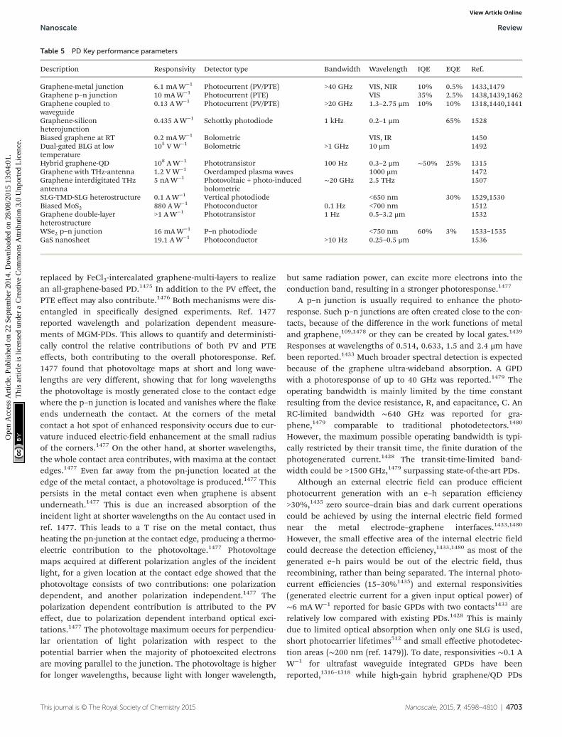
replaced by FeCl3-intercalated graphene-multi-layers to realizean all-graphene-based PD.1475 In addition to the PV effect, thePTE effect may also contribute.1476 Both mechanisms were dis-entangled in specifically designed experiments. Ref. 1477reported wavelength and polarization dependent measure-ments of MGM-PDs. This allows to quantify and deterministi-cally control the relative contributions of both PV and PTEeffects, both contributing to the overall photoresponse. Ref.1477 found that photovoltage maps at short and long wave-lengths are very different, showing that for long wavelengthsthe photovoltage is mostly generated close to the contact edgewhere the p–n junction is located and vanishes where the flakeends underneath the contact. At the corners of the metalcontact a hot spot of enhanced responsivity occurs due to cur-vature induced electric-field enhancement at the small radiusof the corners.1477 On the other hand, at shorter wavelengths,the whole contact area contributes, with maxima at the contactedges.1477 Even far away from the pn-junction located at theedge of the metal contact, a photovoltage is produced.1477 Thispersists in the metal contact even when graphene is absentunderneath.1477 This is due an increased absorption of theincident light at shorter wavelengths on the Au contact used inref. 1477. This leads to a T rise on the metal contact, thusheating the pn-junction at the contact edge, producing a thermo-electric contribution to the photovoltage.1477 Photovoltagemaps acquired at different polarization angles of the incidentlight, for a given location at the contact edge showed that thephotovoltage consists of two contributions: one polarizationdependent, and another polarization independent.1477 Thepolarization dependent contribution is attributed to the PVeffect, due to polarization dependent interband optical exci-tations.1477 The photovoltage maximum occurs for perpendicu-lar orientation of light polarization with respect to thepotential barrier when the majority of photoexcited electronsare moving parallel to the junction. The photovoltage is higherfor longer wavelengths, because light with longer wavelength,
but same radiation power, can excite more electrons into theconduction band, resulting in a stronger photoresponse.1477
A p–n junction is usually required to enhance the photo-response. Such p–n junctions are often created close to the con-tacts, because of the difference in the work functions of metaland graphene,109,1478 or they can be created by local gates.1439
Responses at wavelengths of 0.514, 0.633, 1.5 and 2.4 μm havebeen reported.1433 Much broader spectral detection is expectedbecause of the graphene ultra-wideband absorption. A GPDwith a photoresponse of up to 40 GHz was reported.1479 Theoperating bandwidth is mainly limited by the time constantresulting from the device resistance, R, and capacitance, C. AnRC-limited bandwidth ∼640 GHz was reported for gra-phene,1479 comparable to traditional photodetectors.1480
However, the maximum possible operating bandwidth is typi-cally restricted by their transit time, the finite duration of thephotogenerated current.1428 The transit-time-limited band-width could be >1500 GHz,1479 surpassing state-of-the-art PDs.
Although an external electric field can produce efficientphotocurrent generation with an e–h separation efficiency>30%,1435 zero source–drain bias and dark current operationscould be achieved by using the internal electric field formednear the metal electrode–graphene interfaces.1433,1480
However, the small effective area of the internal electric fieldcould decrease the detection efficiency,1433,1480 as most of thegenerated e–h pairs would be out of the electric field, thusrecombining, rather than being separated. The internal photo-current efficiencies (15–30%1435) and external responsivities(generated electric current for a given input optical power) of∼6 mA W−1 reported for basic GPDs with two contacts1433 arerelatively low compared with existing PDs.1428 This is mainlydue to limited optical absorption when only one SLG is used,short photocarrier lifetimes512 and small effective photodetec-tion areas (∼200 nm (ref. 1479)). To date, responsivities ∼0.1 AW−1 for ultrafast waveguide integrated GPDs have beenreported,1316–1318 while high-gain hybrid graphene/QD PDs
Table 5 PD Key performance parameters
Description Responsivity Detector type Bandwidth Wavelength IQE EQE Ref.
Graphene-metal junction 6.1 mAW−1 Photocurrent (PV/PTE) >40 GHz VIS, NIR 10% 0.5% 1433,1479Graphene p–n junction 10 mAW−1 Photocurrent (PTE) VIS 35% 2.5% 1438,1439,1462Graphene coupled towaveguide
0.13 AW−1 Photocurrent (PV/PTE) >20 GHz 1.3–2.75 μm 10% 10% 1318,1440,1441
Graphene-siliconheterojunction
0.435 AW−1 Schottky photodiode 1 kHz 0.2–1 μm 65% 1528
Biased graphene at RT 0.2 mAW−1 Bolometric VIS, IR 1450Dual-gated BLG at lowtemperature
105 V W−1 Bolometric >1 GHz 10 μm 1492
Hybrid graphene-QD 108 AW−1 Phototransistor 100 Hz 0.3–2 μm ∼50% 25% 1315Graphene with THz-antenna 1.2 V W−1 Overdamped plasma waves 1000 μm 1472Graphene interdigitated THzantenna
5 nAW−1 Photovoltaic + photo-inducedbolometric
∼20 GHz 2.5 THz 1507
SLG-TMD-SLG heterostructure 0.1 AW−1 Vertical photodiode <650 nm 30% 1529,1530Biased MoS2 880 AW−1 Photoconductor 0.1 Hz <700 nm 1512Graphene double-layerheterostructure
>1 AW−1 Phototransistor 1 Hz 0.5–3.2 μm 1532
WSe2 p–n junction 16 mAW−1 P–n photodiode <750 nm 60% 3% 1533–1535GaS nanosheet 19.1 AW−1 Photoconductor >10 Hz 0.25–0.5 μm 1536
Nanoscale Review
This journal is © The Royal Society of Chemistry 2015 Nanoscale, 2015, 7, 4598–4810 | 4703
Ope
n A
cces
s A
rtic
le. P
ublis
hed
on 2
2 Se
ptem
ber
2014
. Dow
nloa
ded
on 2
8/08
/201
5 13
:04:
01.
Thi
s ar
ticle
is li
cens
ed u
nder
a C
reat
ive
Com
mon
s A
ttrib
utio
n 3.
0 U
npor
ted
Lic
ence
.View Article Online
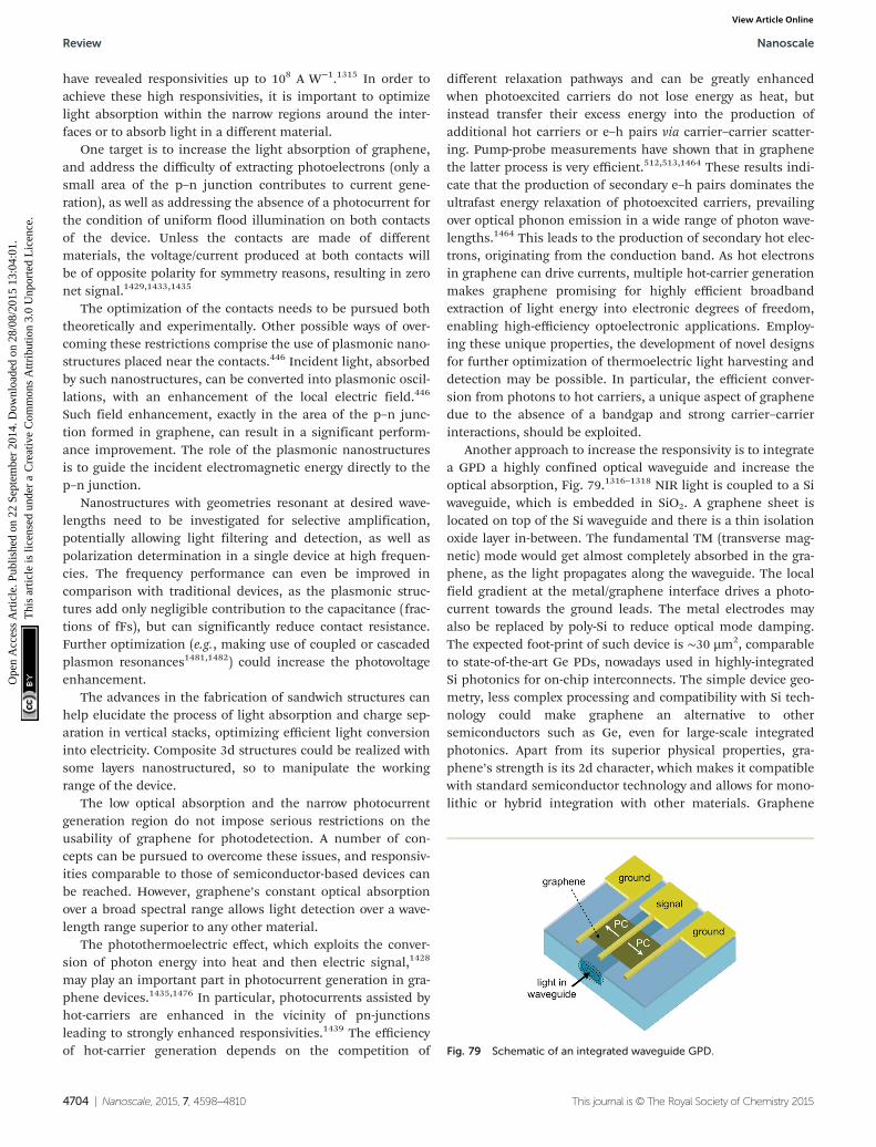
have revealed responsivities up to 108 A W−1.1315 In order toachieve these high responsivities, it is important to optimizelight absorption within the narrow regions around the inter-faces or to absorb light in a different material.
One target is to increase the light absorption of graphene,and address the difficulty of extracting photoelectrons (only asmall area of the p–n junction contributes to current gene-ration), as well as addressing the absence of a photocurrent forthe condition of uniform flood illumination on both contactsof the device. Unless the contacts are made of differentmaterials, the voltage/current produced at both contacts willbe of opposite polarity for symmetry reasons, resulting in zeronet signal.1429,1433,1435
The optimization of the contacts needs to be pursued boththeoretically and experimentally. Other possible ways of over-coming these restrictions comprise the use of plasmonic nano-structures placed near the contacts.446 Incident light, absorbedby such nanostructures, can be converted into plasmonic oscil-lations, with an enhancement of the local electric field.446
Such field enhancement, exactly in the area of the p–n junc-tion formed in graphene, can result in a significant perform-ance improvement. The role of the plasmonic nanostructuresis to guide the incident electromagnetic energy directly to thep–n junction.
Nanostructures with geometries resonant at desired wave-lengths need to be investigated for selective amplification,potentially allowing light filtering and detection, as well aspolarization determination in a single device at high frequen-cies. The frequency performance can even be improved incomparison with traditional devices, as the plasmonic struc-tures add only negligible contribution to the capacitance (frac-tions of fFs), but can significantly reduce contact resistance.Further optimization (e.g., making use of coupled or cascadedplasmon resonances1481,1482) could increase the photovoltageenhancement.
The advances in the fabrication of sandwich structures canhelp elucidate the process of light absorption and charge sep-aration in vertical stacks, optimizing efficient light conversioninto electricity. Composite 3d structures could be realized withsome layers nanostructured, so to manipulate the workingrange of the device.
The low optical absorption and the narrow photocurrentgeneration region do not impose serious restrictions on theusability of graphene for photodetection. A number of con-cepts can be pursued to overcome these issues, and responsiv-ities comparable to those of semiconductor-based devices canbe reached. However, graphene’s constant optical absorptionover a broad spectral range allows light detection over a wave-length range superior to any other material.
The photothermoelectric effect, which exploits the conver-sion of photon energy into heat and then electric signal,1428
may play an important part in photocurrent generation in gra-phene devices.1435,1476 In particular, photocurrents assisted byhot-carriers are enhanced in the vicinity of pn-junctionsleading to strongly enhanced responsivities.1439 The efficiencyof hot-carrier generation depends on the competition of
different relaxation pathways and can be greatly enhancedwhen photoexcited carriers do not lose energy as heat, butinstead transfer their excess energy into the production ofadditional hot carriers or e–h pairs via carrier–carrier scatter-ing. Pump-probe measurements have shown that in graphenethe latter process is very efficient.512,513,1464 These results indi-cate that the production of secondary e–h pairs dominates theultrafast energy relaxation of photoexcited carriers, prevailingover optical phonon emission in a wide range of photon wave-lengths.1464 This leads to the production of secondary hot elec-trons, originating from the conduction band. As hot electronsin graphene can drive currents, multiple hot-carrier generationmakes graphene promising for highly efficient broadbandextraction of light energy into electronic degrees of freedom,enabling high-efficiency optoelectronic applications. Employ-ing these unique properties, the development of novel designsfor further optimization of thermoelectric light harvesting anddetection may be possible. In particular, the efficient conver-sion from photons to hot carriers, a unique aspect of graphenedue to the absence of a bandgap and strong carrier–carrierinteractions, should be exploited.
Another approach to increase the responsivity is to integratea GPD a highly confined optical waveguide and increase theoptical absorption, Fig. 79.1316–1318 NIR light is coupled to a Siwaveguide, which is embedded in SiO2. A graphene sheet islocated on top of the Si waveguide and there is a thin isolationoxide layer in-between. The fundamental TM (transverse mag-netic) mode would get almost completely absorbed in the gra-phene, as the light propagates along the waveguide. The localfield gradient at the metal/graphene interface drives a photo-current towards the ground leads. The metal electrodes mayalso be replaced by poly-Si to reduce optical mode damping.The expected foot-print of such device is ∼30 µm2, comparableto state-of-the-art Ge PDs, nowadays used in highly-integratedSi photonics for on-chip interconnects. The simple device geo-metry, less complex processing and compatibility with Si tech-nology could make graphene an alternative to othersemiconductors such as Ge, even for large-scale integratedphotonics. Apart from its superior physical properties, gra-phene’s strength is its 2d character, which makes it compatiblewith standard semiconductor technology and allows for mono-lithic or hybrid integration with other materials. Graphene
Fig. 79 Schematic of an integrated waveguide GPD.
Review Nanoscale
4704 | Nanoscale, 2015, 7, 4598–4810 This journal is © The Royal Society of Chemistry 2015
Ope
n A
cces
s A
rtic
le. P
ublis
hed
on 2
2 Se
ptem
ber
2014
. Dow
nloa
ded
on 2
8/08
/201
5 13
:04:
01.
Thi
s ar
ticle
is li
cens
ed u
nder
a C
reat
ive
Com
mon
s A
ttrib
utio
n 3.
0 U
npor
ted
Lic
ence
.View Article Online

sheets can be transferred to arbitrary substrates (includingflexible), etched into any shape, integrated with waveguides orcavities, electrically contacted, etc.
All these aspects lead us to consider graphene as a promis-ing new material for photonic integrated circuits,1483 particu-larly for high data-rate optical interconnects. Graphene willallow the realization of high-speed, compact-footprint PDsintegrated with Si waveguides or plasmonic circuits. The mech-anical flexibility of graphene may also enable the integrationwith bendable substrates and low-cost plastic waveguides.Photonic integrated circuits are based on the convergence andco-integration of passive optical components (waveguides,(de-)multiplexers, filters, etc.) with modulators, switches andPDs. State-of-the-art monolithic PDs are based on Ge or III–Vsemiconductors, but their responsivity ranges are spectrallylimited. Graphene, without such a limit due to the gapless dis-persion of the Dirac electrons, could thus pave the way forbroadband photodetection, from the O-band (1260–1360 nm)to the U-band (1625–1675 nm), and beyond (e.g. 850 nm). Theexpected foot-prints of the devices are even smaller than thoseof state-of-the-art Ge devices used in Si photonics. The simpledevice geometry, less complex processing, compatibility withCMOS technology, and broadband and ultra-fast operationcould make graphene an alternative to other materials, evenfor large-scale integrated photonics.
The 2d character of graphene and the possibility of large-area fabrication allows up-scaling from single devices intoarrays. This could enable a pixelated, camera-like structure,where each pixel may be read out individually. Co-integrationwith Si transistors as amplifying elements is envisaged. Thegoal is to achieve gated PD arrays with strongly enhancedresponsivity. The energy spectrum and optical properties ofgraphene can be modified through an electrostatic field. Thiscan be utilized to realize a waveguide-integrated electro-opticalmodulators at 1550 nm, based on optical absorption forphoton energies 2EF < Eph (Eph is the photon energy,EF denotes the Fermi energy) and absorption suppression for2EF > Eph due to Pauli blocking.1339 Graphene-based modulatorscan be realized on a much smaller foot-print than devicesusing semiconductor materials for electro-absorption orelectro-refraction by the Pockels, Kerr1484 and Franz–Keldysheffects.1485,1486
Another target will be the integration of graphene electro-absorption modulators into Si waveguide ring resonators andFabry–Perot cavities with grating mirrors, to further decreasethe foot-print. This will lead to higher modulation depth andspeed than previously reported.
When it comes to high-demand applications, requiringphoton detection at very low levels, even approaching singlephoton detection, photodiodes cannot be chosen, becausetheir quantum efficiency is limited to unity, accounting for 1carrier per photon. Therefore, the electrical signal suffers fromread-out electronic noise, which overwhelms the photocurrentat low intensities. In view of this constraint, gain has beensought in PDs: a mechanism that can provide multiple electri-cal carriers per single incident photon.
Photoconductive detectors are based on the effect of carrierrecirculation,1315 providing Ohmic contacts to the semiconduc-tor and appropriate sensitizing centres that can prolong thecarrier lifetime. Photoconductive gain is then possible, with avalue given by the ratio of the carrier lifetime over the transittime. Photoconductive detectors have regained attention withthe advent of colloidal QDs PDs.1487 Photoconductive gain∼103–105 was reported for PbS, ZnO or CdSe QDs,1487–1489
limited, however, by the low μ of QD films. Phototransistorshave also been proposed to provide for photoconductivegain.1488 A FET-like phototransistor was reported with single-photon counting potential, based on a 2DEG channel and QDsas the photosensitive gate, in an epitaxially grown structure.The 2DEG was formed in an AlGaAs substrate by cooling thedevice to 4 K and it was critical in achieving high sensitivitydue to the high μ that can be achieved in a 2DEG.
Graphene is an excellent candidate for high-gain PDsbecause of the high μ, and since it is 2d. Thus, its conductanceis very sensitive to electrostatic perturbation by photo-generated carriers close to the surface. This makes it a particu-larly promising material for high gain PDs by photogating.Additionally, graphene is a very thin, flexible and durable,and can be fabricated in a large scale and easily depositedon Si, offering integration into standard ICs. Thus, thedemonstration of photodetection gain with graphene would bethe basis for a plethora of applications, such as integratedoptoelectronic circuits, biomedical imaging, remote sens-ing, optical communications, and quantum informationtechnology.
Ultra-sensitive PDs and image sensor arrays for visible andIR imaging have been developed,1315 based on sensitized gra-phene: a film of semiconducting particles or QDs is depositedon the graphene sheet,1315 see Fig. 80. Colloidal QDs offerhigh absorption and bandgap tuneability from UV toSWIR,1488 and could be employed as a vehicle to demonstratethe potential of this technology. Through sensitization, strongabsorption ∼50–100% can be achieved.1315 The detectionmechanism is based on photogating,1490 where light inducedtrapped charges in the QD change the resistance of graphene.
Fig. 80 Schematic of GQD hybrid phototransistor, in which a grapheneflake is deposited onto Si/SiO2 coated with PbS QDs. Incident photonscreate e–h pairs in the PbS QDs. [Adapted from ref. 1315].
Nanoscale Review
This journal is © The Royal Society of Chemistry 2015 Nanoscale, 2015, 7, 4598–4810 | 4705
Ope
n A
cces
s A
rtic
le. P
ublis
hed
on 2
2 Se
ptem
ber
2014
. Dow
nloa
ded
on 2
8/08
/201
5 13
:04:
01.
Thi
s ar
ticle
is li
cens
ed u
nder
a C
reat
ive
Com
mon
s A
ttrib
utio
n 3.
0 U
npor
ted
Lic
ence
.View Article Online

The photoconductive gain associated to this mechanism canbe quantified by the ratio of the lifetime of the trapped carriersin the QD over the drift time of the charge carriers ingraphene. A photoconductive gain ∼108 and responsivity∼107 A W−1 can be achieved,1315 thanks to the high μ of thegraphene channel, and the long carrier lifetime of the photo-generated carriers in the QD layer.1315 In combination with thehigh quantum efficiency >25% and low noise-equivalent-power∼10−17 W, this hybrid QD-GPD is an excellent platform forlarge-scale sensitive SWIR detection.
Research needs to be extended to the mid-IR, targetingbroadband detection in the wavelength range 3–30 µm.Surface plasmon nanostructures functioning as optical anten-nas1491 could be used to couple the long-wavelength radiationto the graphene sheets. In the simplest case, a bow-tie antennaconcentrates the radiation energy to a confined region of sub-wavelength dimension.1445 Asymmetric contacts1433 or, alter-natively, a potential gradient produced by band profile engin-eering can be used to separate the carriers. Antenna arrays willallow scaling the device dimensions to large areas. Due to thelong wavelength of the radiation, the lithography requirementsare relaxed, which will allow cm2-sized detector arrays/camerasby optical lithography. More advanced plasmonic geometriesmay be used to further concentrate the radiation at the metal/graphene interfaces.
7.2.3.1. Bolometers. Bolometric responses have beenmeasured on a biased graphene sheet at RT.1437,1492 Ref. 1437reported that two mechanisms result in bolometric photo-currents with opposite sign. Namely, the T dependence ofμ leads to a reduction of the conductance, while photo-induced excess carriers induce an enhancement of the con-ductance. By changing EF in graphene, one can control whichmechanism dominates.1437 Near the Dirac point, where thecarrier density is lowest, PV effects dominate, while far awayPTE effects dominate.1437
The relative contributions of the two mechanisms dependon the nature of the device, such as the presence and nature ofthe substrate (i.e. polar versus non-polar), the quality of thesample, as expressed by μ, and the experimental conditions,such as the magnitude of applied bias and T. E.g., it wasshown1450 that in a partially supported (on SiO2) and partiallysuspended sample, thermal effects dominate in the suspendedpart, and photovoltaic effects the supported one.
The weak T dependence of the electrical resistance in gra-phene,1493 however, imposes a major challenge for readingdT through electrical transport measurements, and for thisreason a small responsivity of 0.2 mA W−1 was measured forRT graphene bolometric detectors.1437 To solve this problem, adual-gated BLG device with optically transparent top gate wasused1492 to open a band gap at the Dirac point127,1145 andobtain Te-dependent resistance.127 The device was measuredunder MIR illumination (10.6 μm) using a four-terminal con-figuration, and the photoresponse was identified to be bolo-metric.1492 The thermal resistance had a R ∝ T−3.45
dependence, which approximately agrees with the theoreticallyexpected T−3 dependence for (disorder-free) phonon
cooling.1494,1495 The detector exhibits excellent performance:NEP ∼33 fW per √Hz at T = 5 K (several times lower than com-mercial Si or superconducting bolometers) and an intrinsicbandwidth >1 GHz (3–5 orders of magnitude higher). Anotherapproach for implementing a T-dependent graphene resist-ance is to drive the electronic system into the strong localiz-ation regime by adding disorder. This was achieved at low T byusing defective graphene films.1496
Ref. 1497 reported a graphene-superconductor tunnel junc-tion bolometer. When biased within the superconducting gap,the junction resistance is dominated by tunnelling of the ther-mally excited quasi-particles. The increase of Te in grapheneunder illumination decreases the tunnelling resistance, whichcan be probed by a small DC current. For DC signals, the con-tacts are highly resistive due to the superconducting gap,whereas for high-frequency (RF to optical frequencies) signals,the contact has low impedance due to the contact capacitance,therefore the graphene resistance can be matched with that ofan antenna. Although the device in ref. 1497 was measuredwith RF waves, the concept can also be applied for opticaldetection, see ref. 1498 for a recent review.
7.2.3.2. Long-wavelength photodetectors. Applications oflong-wavelength radiation are manifold. The term “long-wave-length” is used to refer to the FIR (THz) and MIR, i.e. the wave-length range 3–1000 μm. Many chemical agents, explosives ornarcotics feature spectral fingerprints in this range.1499 Opto-electronic devices operating in the THz and MIR may beemployed in homeland-security-related applications, e.g. insecurity systems at airports monitoring dangerous substances,but also in environmental-related applications, e.g. gas spec-trometers for air-quality control, whereby traces of threatchemicals have to be detected against a spectral background.At the same time, the MIR spectral range is as well fairlyunexploited, with many interesting imaging and sensing appli-cations in medicine and security.1500
The most sensitive detectors of THz radiation require deepcryogenic cooling: superconducting hot-electron bolo-meters1501 reach NEPs as low as a few fw/Hz1/2 (ref. 1501) withmodulation bandwidths up to the GHz.1501 On the other hand,RT THz detectors are either not very sensitive,1501 or extremelyslow,1501 or operate well only below 1 THz.1501
The situation becomes even more complex when techno-logies that can be produced into matrix arrays are considered.Commercial THz or MIR FPAs are based on microbolometerelements, and provide moderate sensitivities and responsespeeds (NEPs of few pW/Hz1/2 per pixel and ∼1 kHz bandwidthnear 1 THz1501). Recently, Fast electronic devices, based on thegate-modulation of the conductance channel by the incomingradiation (often called plasma-wave detectors1469,1502,1503),have been realized in both HEMT1504 and CMOS1505 architec-tures and show NEPs already competitive with microbolo-meters and response times up to the MHz range.1554 Thistechnology is also scalable to even larger arrays (a 1024 pixelcamera was demonstrated at 0.7 THz1506). For what concernsthe mid-IR, narrow-gap semiconductors, currently used inphotodiode detectors, still suffer from serious problems in
Review Nanoscale
4706 | Nanoscale, 2015, 7, 4598–4810 This journal is © The Royal Society of Chemistry 2015
Ope
n A
cces
s A
rtic
le. P
ublis
hed
on 2
2 Se
ptem
ber
2014
. Dow
nloa
ded
on 2
8/08
/201
5 13
:04:
01.
Thi
s ar
ticle
is li
cens
ed u
nder
a C
reat
ive
Com
mon
s A
ttrib
utio
n 3.
0 U
npor
ted
Lic
ence
.View Article Online

controlling the material quality and poor integrationcapabilities.
GFETs can be exploited to considerably advance the presentstate-of-the-art of plasma-wave detectors, see Fig. 81 (ref.1445), taking advantage of the high μ.1445 This would allowimproved performance in terms of responsivity and band-width, and operation limits well above 1 THz. Even moreappealing is the possibility to reach a regime in which station-ary plasma modes are excited in the transistor channel,leading to resonant, gate tuneable, enhancement of theresponsivity. This also means that the detected radiation wave-length can be controlled by the gate voltage, hence leading toa novel passive spectroscopy system, which is presently notavailable in the THz.1472
Graphene-based broadband THz detectors working at RTwere shown1507 with Rv ∼ 5 nA W−1 and fast response risetimes (∼50 ps) at 2.5 THz, which makes them already suitablefor timing applications. The device employed a log-periodicTHz antenna,1507 with a central interdigitated comb providingthe electrical contact to the SLG.
PTE graphene THz detectors, operating at 2.5 THz andbased on exfoliated SLG with a pattern of asymmetric metalcontacts were also reported.1508 In ref. 1508, the generatedphotoexcited carriers rapidly thermalized due to the strongelectron–electron interactions, while losing energy to thelattice more slowly. The Te gradient drives electron diffusion,and asymmetry, due to dissimilar contact metals, produces anet current via the PTE.
Finally, with the development of large-area growth tech-niques, multi-pixel camera-like arrays are feasible and poten-tially relatively low-cost. The long-term objective is therealization of a graphene THz camera capable of performingpassive imaging and providing spectroscopic information.
7.2.3.3. 2d crystals and hybrids. Although the bulk pro-perties of layered TMDs have been investigated for manydecades,111 their 2d forms have recently attracted much atten-tion due to their potential applications in optoelectronics.1509
The properties of TMDs depend on N. E.g., MoS2 has a bulk
indirect band gap of 1.3 eV, which becomes a direct bandgap of ∼1.8 eV in 1L-MoS2.
1510 This changes the optical pro-perties, such as absorption spectrum and PL. Ref. 378 showeda 1000-fold enhancement of the luminescence quantumyield for 1L compared to bulk MoS2. Valley polarization con-trolled by optical pumping was also demonstrated in1L-MoS2,
1310 and polarization was maintained for longer than1 ns.1511
Compared to classical direct band gap semiconductors,TMDs can also offer additional advantages in the context ofoptoelectronics because of their transparency, mechanicalflexibility and easy processing. This suggests the possibility ofphotovoltaic and photodetection applications in MoS2 andother semiconducting TMDs. PDs made of 1L-MoS2 displayedhigh external photoresponsivity, i.e. the measure of the electri-cal output per optical input, (over 880 A W−1 at 561 nm1512)and a stable photoswitching time of 50 ms.1513 Moreover, theability to tune the bandgap by varying N allows the detectionof light at different wavelengths.1514 The strong photothermo-electric effect measured at metal-MoS2 junctions1515 can alsobe useful for applications in thermopower generation.1515
One important use of layered semiconductors such as MoS2could be in making novel heterojunction devices. E.g., ametal–semiconductor–metal heterojunction photodetector,made of MoS2 and amorphous silicon (a-Si), with rise and falltimes ∼0.3 ms was demonstrated.1516 The transient responseof MoS2/a-Si hybrid PD does not show persistent (residual)photoconductivity, thus making this heterojunction roughly 10times faster with respect to a-Si devices.1516,1517 A photo-responsivity ∼210 mA W−1 was measured for green light, thewavelength used in commercial imaging systems, which is 2–4times larger than that of a-Si.
MoS2 is a good illustration of the wide range of optical pro-perties offered by 2d crystals. These complement those of gra-phene in many ways: graphene is useful for broadband,ultrafast technologies, whereas semiconducting TMDs areadvantageous for applications requiring strong light absorp-tion1529 and electroluminescence.1518 A promising approach tocombine these properties and create multi-functional, highperformance materials consists of assembling graphene withother 2d crystals in heterogeneous stacks and hybriddevices.1519 This new device architecture has lead to noveltransistor concepts based on vertical transport between twographene electrodes, separated by h-BN, MoS2 or WS2layers.106,1520,1529 The same hybrid devices have shown poten-tial for photovoltaic applications with a photoresponsivityabove 0.1 A W−1 and EQE >30%.1529 Graphene layers can beused as work-function tuneable electrodes,1529 while TMDsmay be employed as photoactive material,1529 displaying astrong light–matter interaction and photon absorption. E–hpairs may be created in the TMD and separated between thetwo neighbouring graphene layers, exploiting the whole gra-phene/TMD junction surface to produce photocurrent.1529
The fact that charge carriers in monolayer dichalcogenidesbehave as spin–valley coupled massive Dirac fermions,1521
gives the possibility of building optoelectronic devices exploit-Fig. 81 Antenna-coupled GFET-terahertz detector. The terahertz radi-ation is focused by off-axis parabolic mirrors. Adapted from ref. 1445.
Nanoscale Review
This journal is © The Royal Society of Chemistry 2015 Nanoscale, 2015, 7, 4598–4810 | 4707
Ope
n A
cces
s A
rtic
le. P
ublis
hed
on 2
2 Se
ptem
ber
2014
. Dow
nloa
ded
on 2
8/08
/201
5 13
:04:
01.
Thi
s ar
ticle
is li
cens
ed u
nder
a C
reat
ive
Com
mon
s A
ttrib
utio
n 3.
0 U
npor
ted
Lic
ence
.View Article Online
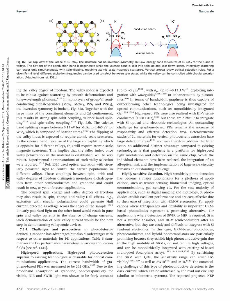
ing the valley degree of freedom. The valley index is expectedto be robust against scattering by smooth deformations andlong-wavelength phonons.1522 In monolayers of group-VI semi-conducting dichalcogenides (MoS2, MoSe2, WS2 and WSe2),the inversion symmetry is broken, Fig. 82a. Together with thelarge mass of the constituent elements and 2d confinement,this results in strong spin–orbit coupling, valence band split-ting1523 and spin–valley coupling,1522 Fig. 82b. The valenceband splitting ranges between 0.15 eV for MoS2 to 0.465 eV forWSe2 which is composed of heavier atoms.1523 The flipping ofthe valley index is expected to require atomic scale scatterers.In the valence band, because of the large spin-splitting whichis opposite for different valleys, this will require atomic scalemagnetic scatterers. This implies that the valley index, oncevalley polarization in the material is established, will be veryrobust. Experimental demonstrations of such valley selectionwere reported.1310 Ref. 1310 used optical excitation with circu-larly polarized light to control the carrier populations indifferent valleys. These couplings between spin, orbit andvalley degrees of freedom distinguish monolayer dichalcogen-ides from other semiconductors and graphene and couldresult in new, as yet unforeseen applications.
The coupled spin, charge and valley degrees of freedommay also result in spin, charge and valley-Hall effects. E.g.,excitation with circular polarizations could generate Hallcurrent, detected as voltage across the edges of the sample.1531
Linearly polarized light on the other hand would result in purespin and valley currents in the absence of charge currents.Such demonstration of pure valley current would be the nextstep in demonstrating valleytronic devices.
7.2.4. Challenges and perspectives in photodetectordevices. Graphene has advantages but also disadvantages withrespect to other materials for PD applications. Table 5 sum-marizes the key performance parameters in various applicationfields [see ref. 1434].
High-speed applications. High-speed photodetectionsuperior to existing technologies is desirable for optical com-munications applications. The current bandwidth of gra-phene-based PDs was measured to be 262 GHz.1327 Due to thebroadband absorption of graphene, photoresponsivity forvisible, NIR and SWIR light was shown to be fairly constant
(up to ∼3 μm1524), with Rph up to ∼0.13 A W−1, exploiting inte-gration with waveguides1316,1318 or enhancements by plasmo-nics.446 In terms of bandwidth, graphene is thus capable ofoutperforming other technologies being investigated foroptical communications, such as monolithically integratedGe.1525,1526 High-speed PDs were also realized with III–V semi-conductors (>300 GHz),1527 but these are difficult to integratewith Si optical and electronic technologies. An outstandingchallenge for graphene-based PDs remains the increase ofresponsivity and effective detection area. Heterostructurestacks of 2d materials for vertical photocurrent extraction havelarge detection areas1529 and may therefore address the latterissue. An additional distinct advantage compared to existingtechnologies is that graphene is a platform for high-speedlight modulation and detection on the same chip. While theindividual elements have been realized, the integration of anall-optical link and the implementation of large-scale circuitryremains an outstanding challenge.
Highly sensitive detection. High sensitivity photo-detectionhas become a major functionality for a plethora of appli-cations, such as remote sensing, biomedical imaging, opticalcommunications, gas sensing etc. For the vast majority ofapplications, such as digital imaging and metrology, Si photo-diodes exhibit excellent performance and are cost-effective dueto their ease of integration with CMOS electronics. For appli-cations where transparency and flexibility is important GRM-based photodiodes represent a promising alternative. Forapplications where detection of SWIR to MIR is required, Si isnot a suitable absorber, and III–V semiconductors offer analternative, but they are costly and difficult to integrate with Siread-out electronics. In this case, GRM-based photodiodes,photoconductors and hybrid phototransistors are particularlypromising because they exhibit high photoconductive gain dueto the high mobility of GRMs, do not require high voltages,and can be monolithically integrated with existing Si-basedmulti-pixel focal-plane arrays.1315,1443,1444,1537 By sensitizingthe GRM with QDs, the sensitivity range can cover UV-visible,1538,1539 as well as SWIR1487 and MIR.1540 The outstand-ing challenge of this type of photoconductive detectors is thedark current, which can be addressed by the read-out circuitry(similar to bolometric systems). The reported projected NEP
Fig. 82 (a) Top view of the lattice of 1L-MX2. The structure has no inversion symmetry. (b) Low-energy band structures of 1L-MX2 for the K and K’valleys. The bottom of the conduction band is degenerate while the valence band is split into spin-up and spin down states. Intervalley scatteringcan occur only simultaneously with spin-flipping, requiring atomic scale magnetic scatterers. Vertical arrows show optical selection rules. For agiven Fermi level, different excitation frequencies can be used to select between spin states, while the valley can be controlled with circular polariz-ation. [Adapted from ref. 1521].
Review Nanoscale
4708 | Nanoscale, 2015, 7, 4598–4810 This journal is © The Royal Society of Chemistry 2015
Ope
n A
cces
s A
rtic
le. P
ublis
hed
on 2
2 Se
ptem
ber
2014
. Dow
nloa
ded
on 2
8/08
/201
5 13
:04:
01.
Thi
s ar
ticle
is li
cens
ed u
nder
a C
reat
ive
Com
mon
s A
ttrib
utio
n 3.
0 U
npor
ted
Lic
ence
.View Article Online
(∼10−17 W) and specific detectivity D* (7 × 10¹³ Jones)1315 areon par with existing technologies, such as InGaAs. Outstand-ing challenges include improvement in speed (currently up to100 Hz), large-scale production and integration of multi-pixelarrays. Alternatively, p–n photodiode-based TMDs exhibit highsensitivity (see e.g. ref. 1534, 1535) and low dark current. Out-standing challenges include the improvement of the sensitivearea and large-scale production.
Mid-infrared detection. The detection of MIR light is impor-tant for bio-sensing, security, thermal imaging, etc. For thisfrequency range, graphene can offer an appealing advantagecompared to other materials, by employing plasmons, whichresonantly enhance absorption for a wavelength that is tunableby a gate, offering in situ tunable spectral selectivity. Themajor outstanding challenge for this wavelength range is thecarrier extraction, e.g. by utilizing p–n junctions in lateral orvertical structures, or by employing bolometric detection. Gra-phene bolometers have shown excellent performance1492 atlow temperature, with NEP ∼ 33 fW per √Hz, comparable toexisting technologies. The main challenge remains the match-ing of the high graphene impedance (tens of kΩ) to that offree space (377 Ω) for efficient photon coupling.
Terahertz detection. Photodetection of FIR radiation is sig-nificant for a variety of applications, ranging from medicaldiagnostics to process control, homeland security and culturalheritage. Commercially available THz detectors are based onthermal sensing elements that are either very slow (10–400 Hzmodulation and NEP ∼ 10−10 W per √Hz) or require deep cryo-genic cooling (4 K for superconducting hot-electron bol-ometers), while those exploiting fast nonlinear electronics(Schottky diodes) or high-mobility transistors are usuallylimited to sub-THz frequencies.1541 Graphene can exceed theselimits by exploiting THz plasma waves that are weakly dampedin high-quality samples, allowing for resonant detectionregimes in a FET. This could potentially beat all other techno-logies at RT, but a major challenge is the demonstration of theresonant DS detection mechanism1468,1469 by integrating high-mobility graphene with appropriate THz antennas. However,graphene THz detectors have already been demonstrated forthe range 0.29–0.38 THz with a NEP ∼ 10−9 W per √Hz,1445
and for the range 2 THz with a NEP ∼ 10−8 W per √Hz.1508
The combination of scalability at higher frequencies, the pro-spects for integration with Si-platforms as well as the potentialfor implementing flexible devices, makes graphene highlycompetitive for a future generation of THz detection systems.
Although photodetection platforms based on GRMs havebeen developed for a wide variety of applications at a remark-able pace, outstanding challenges remain to demonstrate thetrue potential and to exploit the distinct advantages of 2d crys-tals. The prospects for commercialization will not just dependon the detector performance, but likely also on some of thedistinct advantages and capabilities, in addition to the abilityto realize production of large-scale high-quality 2d materialsat a low-cost, and to establish large-scale integration with exist-ing photonic and electronic platforms, such as CMOStechnologies.
7.3. Graphene plasmonics
Photonic technologies, based on light–matter interactions,already have a significant slice of today’s markets.1542 With theadvent of nanofabrication, light–matter interactions can nowbe studied and tailored at a fundamental level. Of recent inter-est is the use of metallic nanoparticles (MNPs), where surfaceplasmon resonances (SPRs) greatly enhance light–matter inter-actions.1543 SPRs are characterized by a large extinction crosssection and the electromagnetic field is amplified by severalorders of magnitude nearby the resonant MNPs.1543 Becauseof the near-field focusing at the SPR, every photoelectricalactivity, such as absorption and emission, gets enhanced onthe MNP surface. At high enough intensity, these two effectsget coupled in a nonlinear manner exhibiting novel pheno-mena. Plasmon resonances can be tuned by acting on theshape654 and on the mutual interactions of the MNPs.1544 Thedynamics of the plasmon resonance is extremely fast: ∼10 fsfor plasmon dephasing,1545 ∼100 fs for equilibration into a hotelectron distribution via e–e scattering1545 and ∼1 ps for relax-ation via phonon emission.1545 Plasmonic nanostructures areusually characterized by good thermal1546,1547 and chemicalstability1548,1549 and can be functionalized by chemical reac-tions on the surface.1550,1551 Finally, the noble metals are excel-lent electrical conductors.1552
The combinations of semiconductor quantum dots (SQD)with MNPs1553 allows the study of the strong coupling regime,in which there is reversible exchange of energy between theemitter and the MNP (cavity) mode, giving rise to mixed light–matter cavity-polariton modes.1553 This mode, the physics ofwhich is most conveniently described by a combination of clas-sical and quantum mechanics,1553 has possible applications ina broad range of fields, including quantum information, inter-facing of electronic and photonic components, surfaceplasmon lasers, solar energy harvesting, sensors and actuators.Over the past few years, hybrid SQD-MNP structures weremanufactured in order to combine the discrete excitonicresponse with the strong optical response of plasmons.1554 Inthese structures, long-range Coulomb interaction couples thetwo subsystems creating hybrid exciton-plasmon excitations,resulting into Förster energy transfer,1555 Rabi charge oscil-lations,1556 nonlinear Fano resonances1554 and bistability.1557
Surface plasmon amplification by stimulated emission of radi-ation, where, rather than amplifying light in a conventionallaser cavity, a plasmonic ‘spacer’ amplifies it with the help ofplasmons, was used to develop nanolasers.1558
Graphene is poised to make a significant impact in modernphotonics. A large part of this will be enabled by the advent ofplasmonics to enhance and facilitate light–matter interactions.Recent work has shown the benefit of MNP in graphene-basedphotonic applications, such as graphene PVs446 and SERS.1333
Intrinsic graphene plasmons provide a suitable alternative tonoble-metal plasmons due to their much larger confine-ment1313 and long propagation distances,1313 with the advan-tage of being tuneable via electrostatic gating.1313,1321
Compared to conventional plasmonic metals, graphene can
Nanoscale Review
This journal is © The Royal Society of Chemistry 2015 Nanoscale, 2015, 7, 4598–4810 | 4709
Ope
n A
cces
s A
rtic
le. P
ublis
hed
on 2
2 Se
ptem
ber
2014
. Dow
nloa
ded
on 2
8/08
/201
5 13
:04:
01.
Thi
s ar
ticle
is li
cens
ed u
nder
a C
reat
ive
Com
mon
s A
ttrib
utio
n 3.
0 U
npor
ted
Lic
ence
.View Article Online
lead to much larger field enhancements and optical fieldconfinement.1313
7.3.1. Hybrid graphene-plasmon systems. The combi-nation of graphene photonics with plasmonics, whereby thelight interaction is modulated and enhanced by placing arraysof metal particles or antennas on the graphene surface, canimprove the performance of existing devices, overcoming somelimitations associated with the transparency of graphene inthe visible-NIR. SQD-sensitised GQDs (Fig. 80) can lead tostrong photovoltage enhancements.446,1315 Graphene-plasmo-nics could pave the way towards novel sensing routes, bymodulation of the metal dielectric function.
Graphene-MNP-SQD complexes might play an importantrole in future optoelectronic and quantum informationtechnologies. The target is to develop hybrid graphene-plasmo-nic devices with higher performance than non-hybrid devices.The interaction between graphene nanodisks or ribbons withmetallic nanostructures can be exploited for the realization ofoptical switches and single photon devices,1559 taking advan-tage of GSA and the local electromagnetic field amplificationinduced by localized surface plasmons. Such hybrids arepromising candidates for the realization of nano-opticaldevices, such as ultrafast nano-optical switches, surfacePlasmon-polariton amplifiers, lasers, IR detectors, single-photon quantum devices, and ultrasensitive detectors.Enhancement of energy transfer is also important in solarenergy applications, such as in DSSCs, where facilitation ofdye–MNP interactions may play an important role in improvingperformance. Graphene can be made luminescent,689 thus itsinteraction with MNPs can be exploited to enhance and tailorits emission properties.
Sensitive photodetection in the SWIR would enable passivenight vision1560,1561 from 1 to 1.7 μm, and biomedical imagingfor tumour detection,1562 exploiting the tissue transparentwindows around 900 and 1100 nm.1563,1564 Additional appli-cation are astrophysics,1565 remote sensing for climate andnatural resources monitoring,1566 food and pharmaceuticalindustries for quality control and product inspection1567 andidentification.1568
Modelling of the optical properties, such as extinction,absorption, and scattering cross-sections, as well as local fieldenhancement in the proximity of metallic nanostructures dueto plasmon resonances1569 is important, in order to predicttheir functions and to engineer their properties. It is thusnecessary to achieve a thorough understanding of the inter-action between the subsystems and how their individualoptical properties contribute to the formation of novel effects.Advanced computer models for the optical response of theconstituent subsystems, incorporating both photonic and elec-tronic degrees of freedom in a direct time-domain semi-classi-cal approach are needed. Finite element methods such as theDiscrete Dipole Approximation (DDA)1570 and time domainmethods, such as the Finite-Difference Time-Domain(FDTD),1571 represent some of the most effective and versatilesolutions for modelling the optical properties of nano-structures with complex form and hybrid composition.
Another important issue that needs to be addressed is theresponse of molecules or SQD that are very close to the MNPor graphene surface, due to the nonlocal response of the metaland graphene dielectric functions. This may have an importantrole on the actual field enhancement and energy transfer rates.An explicit scheme for taking into account spontaneous emis-sion also needs to be implemented. Such a rich model inven-tory to describe graphene, metals and active materials willenable the detailed time-resolved simulation of novel gra-phene-based photonic and plasmonic devices. This modellingcapability will facilitate the design of future graphene-basedphotonic and plasmonic applications.
The large-scale realization of hybrid devices will require ver-satile preparation techniques with high control on the surfaceof metal nanostructures. In some cases, a high degree ofpurity will be required for the metal–graphene contacts, whilein other cases the ability to self-assemble the metal and gra-phene components will be needed. This could achieved viathe insertion of appropriate synthetic mediators, such asmolecules anchored on the surface of plasmonic nano-structures. The control of the surface of the plasmonic nano-structures will play a key role in the realization of hybriddevices. Some devices will require ultra-clean interfacesbetween graphene and metal nanostructures, which can onlybe obtained through ultra-clean chemical free techniques ofsynthesis. In other cases, the creation of ordered structures ona large scale may be achieved through self-assembly of plasmo-nic nanostructures and graphene, which can be guided by anintermediate molecule, eventually bound to the surface ofmetal nanostructures by exploiting the surface chemistry ofnoble metals.1572 Laser ablation synthesis in solution of plas-monic nanostructures has the potential for fulfilling a largepart of the above requirements.654,1573
Graphene can be combined with plasmonic meta-materials.1574 This promises more effective conversion of lightinto electricity,446 extremely sensitive sensors based on opticaltransduction1575 and a possibility to realize materials withoptical properties that could be governed by the graphenegating, often referred to as active plasmonics.1576 Challengesin combining plasmonics with graphene include control ofdoping, and problems with graphene gating caused by thepresence of the plasmonic metamaterial. Small, fast and cheapoptical modulators based on graphene-based plasmonic meta-materials could be used in optoelectronics to enhance thespeed of internet. More efficient photocells which make use ofa larger part of the solar spectrum and produce more electri-city under the same illumination. Extremely sensitive opticalplasmonic nanosensors coupled with graphene could pushforward optical transduction methods.
7.3.2. Intrinsic graphene plasmons. Graphene surfaceplasmons (GSPs) provide an appealing alternative to noble-metal plasmons because they display a range of potentiallyuseful properties. GSPs exhibit a wavelength compressionfactor of the plasmon wavelength with respect to the free-spacewavelength ∼200–300,1321 one to two orders of magnitudehigher than for noble metals.1321
Review Nanoscale
4710 | Nanoscale, 2015, 7, 4598–4810 This journal is © The Royal Society of Chemistry 2015
Ope
n A
cces
s A
rtic
le. P
ublis
hed
on 2
2 Se
ptem
ber
2014
. Dow
nloa
ded
on 2
8/08
/201
5 13
:04:
01.
Thi
s ar
ticle
is li
cens
ed u
nder
a C
reat
ive
Com
mon
s A
ttrib
utio
n 3.
0 U
npor
ted
Lic
ence
.View Article Online
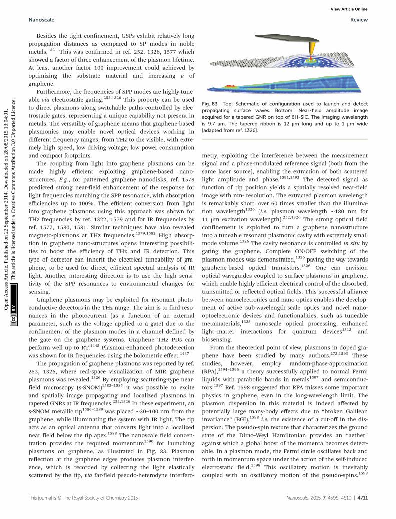
Besides the tight confinement, GSPs exhibit relatively longpropagation distances as compared to SP modes in noblemetals.1321 This was confirmed in ref. 252, 1326, 1577 whichshowed a factor of three enhancement of the plasmon lifetime.At least another factor 100 improvement could achieved byoptimizing the substrate material and increasing μ ofgraphene.
Furthermore, the frequencies of SPP modes are highly tune-able via electrostatic gating.252,1326 This property can be usedto direct plasmons along switchable paths controlled by elec-trostatic gates, representing a unique capability not present inmetals. The versatility of graphene means that graphene-basedplasmonics may enable novel optical devices working indifferent frequency ranges, from THz to the visible, with extre-mely high speed, low driving voltage, low power consumptionand compact footprints.
The coupling from light into graphene plasmons can bemade highly efficient exploiting graphene-based nano-structures. E.g., for patterned graphene nanodisks, ref. 1578predicted strong near-field enhancement of the response forlight frequencies matching the SPP resonance, with absorptionefficiencies up to 100%. The efficient conversion from lightinto graphene plasmons using this approach was shown forTHz frequencies by ref. 1322, 1579 and for IR frequencies byref. 1577, 1580, 1581. Similar techniques have also revealedmagneto-plasmons at THz frequencies.1579,1582 High absorp-tion in graphene nano-structures opens interesting possibili-ties to boost the efficiency of THz and IR detection. Thistype of detector can inherit the electrical tuneability of gra-phene, to be used for direct, efficient spectral analysis of IRlight. Another interesting direction is to use the high sensi-tivity of the SPP resonances to environmental changes forsensing.
Graphene plasmons may be exploited for resonant photo-conductive detectors in the THz range. The aim is to find reso-nances in the photocurrent (as a function of an externalparameter, such as the voltage applied to a gate) due to theconfinement of the plasmon modes in a channel defined bythe gate on the graphene systems. Graphene THz PDs canperform well up to RT.1445 Plasmon-enhanced photodetectionwas shown for IR frequencies using the bolometric effect.1437
The propagation of graphene plasmons was reported by ref.252, 1326, where real-space visualization of MIR grapheneplasmons was revealed.1326 By employing scattering-type near-field microscopy (s-SNOM)1583–1585 it was possible to exciteand spatially image propagating and localized plasmons intapered GNRs at IR frequencies.252,1326 In these experiment, ans-SNOM metallic tip1586–1589 was placed ∼30–100 nm from thegraphene, while illuminating the system with IR light. The tipacts as an optical antenna that converts light into a localizednear field below the tip apex.1588 The nanoscale field concen-tration provides the required momentum1590 for launchingplasmons on graphene, as illustrated in Fig. 83. Plasmonreflection at the graphene edges produces plasmon interfer-ence, which is recorded by collecting the light elasticallyscattered by the tip, via far-field pseudo-heterodyne interfero-
metry, exploiting the interference between the measurementsignal and a phase-modulated reference signal (both from thesame laser source), enabling the extraction of both scatteredlight amplitude and phase.1591,1592 The detected signal asfunction of tip position yields a spatially resolved near-fieldimage with nm- resolution. The extracted plasmon wavelengthis remarkably short: over 60 times smaller than the illumina-tion wavelength1326 (i.e. plasmon wavelength ∼180 nm for11 μm excitation wavelength).252,1326 The strong optical fieldconfinement is exploited to turn a graphene nanostructureinto a tuneable resonant plasmonic cavity with extremely smallmode volume.1326 The cavity resonance is controlled in situ bygating the graphene. Complete ON/OFF switching of theplasmon modes was demonstrated,1326 paving the way towardsgraphene-based optical transistors.1326 One can envisionoptical waveguides coupled to surface plasmons in graphene,which enable highly efficient electrical control of the absorbed,transmitted or reflected optical fields. This successful alliancebetween nanoelectronics and nano-optics enables the develop-ment of active sub-wavelength-scale optics and novel nano-optoelectronic devices and functionalities, such as tuneablemetamaterials,1323 nanoscale optical processing, enhancedlight–matter interactions for quantum devices1313 andbiosensing.
From the theoretical point of view, plasmons in doped gra-phene have been studied by many authors.273,1593 Thesestudies, however, employ random-phase-approximation(RPA),1594–1596 a theory successfully applied to normal Fermiliquids with parabolic bands in metals1597 and semiconduc-tors.1597 Ref. 1598 suggested that RPA misses some importantphysics in graphene, even in the long-wavelength limit. Theplasmon dispersion in this material is indeed affected bypotentially large many-body effects due to “broken Galileaninvariance” (BGI),1598 i.e. the existence of a cut-off in the dis-persion. The pseudo-spin texture that characterizes the groundstate of the Dirac–Weyl Hamiltonian provides an “aether”against which a global boost of the momenta becomes detect-able. In a plasmon mode, the Fermi circle oscillates back andforth in momentum space under the action of the self-inducedelectrostatic field.1598 This oscillatory motion is inevitablycoupled with an oscillatory motion of the pseudo-spins.1598
Fig. 83 Top: Schematic of configuration used to launch and detectpropagating surface waves. Bottom: Near-field amplitude imageacquired for a tapered GNR on top of 6H-SiC. The imaging wavelengthis 9.7 μm. The tapered ribbon is 12 μm long and up to 1 μm wide[adapted from ref. 1326].
Nanoscale Review
This journal is © The Royal Society of Chemistry 2015 Nanoscale, 2015, 7, 4598–4810 | 4711
Ope
n A
cces
s A
rtic
le. P
ublis
hed
on 2
2 Se
ptem
ber
2014
. Dow
nloa
ded
on 2
8/08
/201
5 13
:04:
01.
Thi
s ar
ticle
is li
cens
ed u
nder
a C
reat
ive
Com
mon
s A
ttrib
utio
n 3.
0 U
npor
ted
Lic
ence
.View Article Online

Since the exchange interactions depend on the relative orien-tation of pseudo-spins,1598 they contribute to plasmon kineticenergy and renormalize its frequency even at leading order inmomentum.1598
It will be important to study the impact of BGI on theplasmon energy-momentum dispersion. This can be sup-pressed by e.g. inserting a sufficient number of BN layersbetween two SLGs. Since Coulomb interactions are long-ranged, one can achieve a regime in which inter-layer tunnel-ling is negligible, while e–e interactions are not. The intrinsicplasmon lifetime due to e–e interactions also needs to becalculated.
The study of plasmons and magneto-plasmons in graphenemay be performed by means of electronic Raman experiments.This approach was extensively used for the investigationsof plasmons and magneto-plasmons in ordinary semiconduc-tor heterostructures,1599 but its application to graphenehas been limited by the absence of favourable inter-band orintra-band resonant conditions matching the energy ofavailable lasers. Indeed, light scattering can probe magneto-plasmons177,183,209,211,1600,1601 and coupled phonon-magneto-plasmons in SLG. The extension of these efforts to the study ofplasmons and plasmon dispersions, in connection to thetheoretical analysis discussed above, would provide newadvances in fundamental understanding of graphene and willset the physical basis for the development of the THz detectortechnology.
Metamaterials and transformation optics,1602–1605 (i.e.media, possibly made of metamaterials, designed in such away that they appear to perform a coordinate transformationfrom physical space to some virtual electromagnetic space1602)provide schemes for devices such as nanoscale waveguides,and superlenses.1606 Graphene metamaterials are promising,since electromagnetic field patterns can be tailored with nano-scale resolution and ultra-high speed through gate-tunablepotential landscapes.
7.4. Graphene-based antennas
Throughout the last decades, communication has beenenabled among different entities, ranging from mainframes tolaptops and sensors. Along with the progressive shrinking insize of devices, engineers have developed efficient communi-cation means tailored to the peculiarities of each type ofdevice. The resulting networks have expanded the applicationsof the individual nodes by providing them a mechanism tocooperate. A good example of such applications is the Internet.The main challenge to enable communications among nano-machines, and at the nanoscale, is that reducing the size of aclassical metallic antenna down to a few hundred nm wouldimpose the use of extremely high resonant frequencies.1607
Graphene-based nanoantennas (width: few nanometres,length: tens of micrometres) could be a key technology to over-come this issue, since this material supports the propagationof tightly confined SPPs.1608,1609 Due to their high effectivemode index,1610 the SPP propagation speed can be up to twoorders of magnitude below the EM wave propagation speed in
vacuum. The main consequence is to reduce the resonant fre-quency of the antenna.1611 Recent works1612,1613 point to THzbands at short ranges, thereby enabling Graphene-enabledWireless Communications (GWC).1158
The particularities of wireless communications at the nano-scale, their applications, and those aspects specificallyinherent to GWC, such as the THz band, require that well-established communication protocols and network architec-tures undergo a profound revision in order to be applied tothis scenario. One must develop a radically new mediumaccess control (MAC), which provides channel access controlmechanisms that make it possible for network nodes to com-municate within a multiple access network, routing andaddressing protocols along with network paradigms for GWC.
GWC might enable a variety of ICT applications. First,embedding nano-antennas into multi-core processors, allow-ing them to scale up to thousands of cores, and overcomingthe challenge of global wiring and the associated delay. Thismulti-core architecture is known as Wireless Network-on-Chip(WNC).1614 Second, GWC may allow networks of small sensorsthat can measure nanoscale magnitudes with unprecedentedaccuracy. Nanosensors might measure physical characteristicsof structures a few nm in size, chemical compounds in concen-trations as low as one part per billion, or the presence of bio-logical agents. Such networks of sensors, known as WirelessNanoSensor Network (WNSN),1615 are, per se, a new network-ing paradigm. WNSN require the integration of several nano-electronic components and could be commercially feasible in20 years from now. Third, GWC may enable communicationsin any device, regardless of its size. In this context, long-awaited applications such as true Ubiquitous Computing orProgrammable Matter,1616 a material which inherently has theability to perform information processing, may be possiblewith GWC. These applications may change the way in whichsociety understands and interacts with technology, and pushthe boundaries of what technology can achieve.
Moreover, the flexibility of graphene coupled with the highσ74 and transparency,990 make it a good candidate for printedantennas on top of touch screens on smartphones. Tradition-ally, these types of antennas are based on ITO.1617 Further-more, the variable resistivity can also lead to graphene’s use inantenna design applications, as a smart material where itsconductivity can be adapted according to external stimuli.Reconfigurable antennas may be designed controlling the radi-ation pattern and efficiency, depending on the application.1618
E.g., stacking several layers of graphene the conductivityand bandgap could also be tuned. Therefore, graphene’s pro-perties could be tuned either by an external electric field, orthrough an interaction-induced symmetry breaking betweenseveral layers, thus leading to atomically-thin insulators orconductors.
7.5. Hybrid graphene-nanocrystal for light emitting devices
Shape controlled semiconductor core/shell colloidal inorganicnanocrystals (CINs) show advantageous luminescent pro-perties,1619 including high quantum yield1620 and the possi-
Review Nanoscale
4712 | Nanoscale, 2015, 7, 4598–4810 This journal is © The Royal Society of Chemistry 2015
Ope
n A
cces
s A
rtic
le. P
ublis
hed
on 2
2 Se
ptem
ber
2014
. Dow
nloa
ded
on 2
8/08
/201
5 13
:04:
01.
Thi
s ar
ticle
is li
cens
ed u
nder
a C
reat
ive
Com
mon
s A
ttrib
utio
n 3.
0 U
npor
ted
Lic
ence
.View Article Online
bility to precisely tailor their emission wavelength by tuningthe core size.1620 The organization of such CINs into orderedarrays, e.g. micro scale ensembles of laterally and verticallyaligned nanorods, has been achieved, with promising opto-electronic properties.1621
Graphene can open up new horizons in terms of designinghybrid architectures consisting of light emitting semiconduc-tor CINs1622,1623 and plasmonic MNPs.1624 Apart from beingthe scaffold for complex assembly structures, graphene cancontribute to the functionality due to its electrical properties,which can be used for charge transport, but also for modu-lation of electrical interaction between metal and semiconduc-tor NPs.
The aims are: (i) fabrication of homogenous and preferablyordered CIN layers on graphene, (ii) using graphene as a tem-plate for more complex NC assemblies, (iii) implementing gra-phene as a interface between metal NPs for plasmonics andsemiconductor CINs for enhanced light emission, (iv) optimiz-ing the graphene-NC interface for achieving efficient chargeinjection into semiconductor CINs while maintaining theirbright emission, (iii) design of novel device architecturesexploiting the flexibility of graphene.
The first aim is the controlled fabrication of NC layers ongraphene surfaces in bilayer and multilayer configurations forlight emitting applications, and the efficient charge injectionfrom graphene into the CIN layer. In a 10 years perspective thetarget is the bottom-up approach to graphene-CIN based elec-trically-pumped LEDs and lasers, in which the optical gainmaterial also constitutes the resonant cavity.
7.6. Graphene-based nanoscale optical routing and switchingnetworks
The combination of graphene’s electronic and photonic pro-perties with its large-scale manufacturability and compatibilitywith Si technology make it a promising candidate for photonicintegrated circuits.1483 These are based on the convergenceand co-integration of a large number of passive optical com-ponents (such as waveguides, (de-)multiplexers, and filters)with active optoelectronic devices (modulators, switches andPDs) on a single chip. In most of the existing technologies, thetypical length-scale of these active elements is large. Electro-absorption modulators and switches may be realized foroptical, infrared and THz frequencies, at smaller length-scales.These devices, together with waveguide-integrated graphenePDs, might provide a toolbox of optoelectronic components forhighly integrated optical interconnects.
Specifically, graphene electro-optical modulators for visibleand NIR frequencies could be integrated with Si waveguides.The energy spectrum and optical properties of graphene canbe modified through an electrostatic field.1314 This was uti-lized to realize a broadband electro-absorption modulator,1314
based on optical absorption for photon energies 2EF < Eph andabsorption suppression for 2EF > Eph due to Pauli blocking.1314
Due to the strong light–matter interaction (2000 dB cm−1
absorption1625), graphene-based modulators and switches maybe realized on a smaller foot-print than devices using semicon-
ductors, for electro-absorption or electro-refraction by thePockels (i.e. birefringence in an optical medium induced by aconstant or varying electric field1626), Kerr (i.e. change in therefractive index of a material in response to an applied electricfield1627) and Franz–Keldysh (i.e. change in optical absorptionin response to an electric field1628) effects. In order to achieveeven higher integration densities and operation frequencies,ring resonators1629 and Fabry–Perot cavities with gratingmirrors1630 are need. This might lead to higher modulationdepth and speed than previously reported. The target shouldbe operation at data rates >10 GBit s−1.
Alternatively, by combining graphene with plasmonics, itmay be possible to enhance light–graphene interactions andachieve deeper modulation with smaller device size. Twoalternatives, with optimized designs for modulation contrastand wavelength range, can be envisaged: (A) Fabrication andoptimization of dielectric loaded plasmonic waveguidescoupled with graphene aiming to achieve deep and highspeed light modulation using low voltage graphene gating.These devices will operate from visible to NIR frequencies.(B) Exploitation of intrinsic graphene plasmons, for the wave-length range 2–10 μm, for which plasmons can be switchedwith virtually infinite on/off ratio.1326 By shaping grapheneinto 1d plasmonic waveguides, and with local electrostaticgating, the functionality of a nanoscale photon transistor maybe realized. In addition, these plasmonic waveguides may becoupled to dielectric waveguides to interface with dielectric-based photonics to minimize losses.
The techniques and devices discussed above may be inte-grated in large-scale devices, to achieve M × 10 Gbit s−1 (withM the number of WDM channels) on-chip data transmission.The advantages of using graphene for photonic integratedcircuits are manifold: simplicity, broadband operation, smallfootprint, and CMOS compatibility.
Graphene also offers a unique possibility to make electri-cally tuneable and ultrathin polarization modulators in theTHz range and potentially up to MIR. Major applications, suchas biosensing, pharmaceutical research, ultrafast wireless com-munications and environmental pollution control may benefitsignificantly from THz spectroscopy. Active control of theoptical polarization is central for numerous applications incommunication technology and optical physics, for materialcharacterization and research methods. In the vast majority ofapplications the polarization is either fixed or controlledslowly by mechanical motion of the polarizing elements.Magneto-optical elements, such as Faraday rotators1631
(i.e. devices that rotates the polarization of light due to theFaraday effect) are typically thick because of the small Verdetconstants, which give a quantitative measure of the Faradayrotation ability of the material.1631 This prevents using them incompact optical circuits, with a lack of broadband or spectrallytunable optical rotators.
The timeline is shown in Fig. 84 and the main targets forphotonics and optoelectronics are: 3 years: Tunable meta-materials, plane-wave THz detection, electro-absorption andplasmon-based optical switches, graphene PDs for visible and
Nanoscale Review
This journal is © The Royal Society of Chemistry 2015 Nanoscale, 2015, 7, 4598–4810 | 4713
Ope
n A
cces
s A
rtic
le. P
ublis
hed
on 2
2 Se
ptem
ber
2014
. Dow
nloa
ded
on 2
8/08
/201
5 13
:04:
01.
Thi
s ar
ticle
is li
cens
ed u
nder
a C
reat
ive
Com
mon
s A
ttrib
utio
n 3.
0 U
npor
ted
Lic
ence
.View Article Online
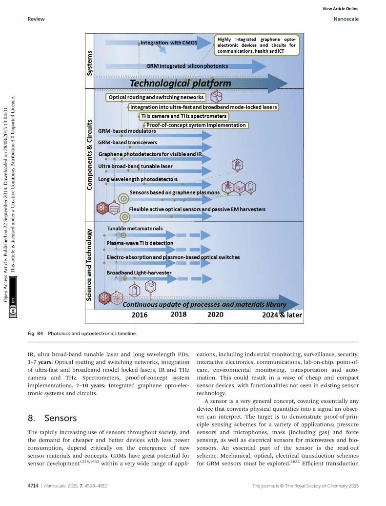
IR, ultra broad-band tunable laser and long wavelength PDs.3–7 years: Optical routing and switching networks, integrationof ultra-fast and broadband model locked lasers, IR and THzcamera and THz. Spectrometers, proof-of-concept systemimplementations. 7–10 years: Integrated graphene opto-elec-tronic systems and circuits.
8. Sensors
The rapidly increasing use of sensors throughout society, andthe demand for cheaper and better devices with less powerconsumption, depend critically on the emergence of newsensor materials and concepts. GRMs have great potential forsensor development1326,1632 within a very wide range of appli-
cations, including industrial monitoring, surveillance, security,interactive electronics, communications, lab-on-chip, point-of-care, environmental monitoring, transportation and auto-mation. This could result in a wave of cheap and compactsensor devices, with functionalities not seen in existing sensortechnology.
A sensor is a very general concept, covering essentially anydevice that converts physical quantities into a signal an obser-ver can interpret. The target is to demonstrate proof-of-prin-ciple sensing schemes for a variety of applications: pressuresensors and microphones, mass (including gas) and forcesensing, as well as electrical sensors for microwaves and bio-sensors. An essential part of the sensor is the read-outscheme. Mechanical, optical, electrical transduction schemesfor GRM sensors must be explored.1632 Efficient transduction
Fig. 84 Photonics and optoelectronics timeline.
Review Nanoscale
4714 | Nanoscale, 2015, 7, 4598–4810 This journal is © The Royal Society of Chemistry 2015
Ope
n A
cces
s A
rtic
le. P
ublis
hed
on 2
2 Se
ptem
ber
2014
. Dow
nloa
ded
on 2
8/08
/201
5 13
:04:
01.
Thi
s ar
ticle
is li
cens
ed u
nder
a C
reat
ive
Com
mon
s A
ttrib
utio
n 3.
0 U
npor
ted
Lic
ence
.View Article Online
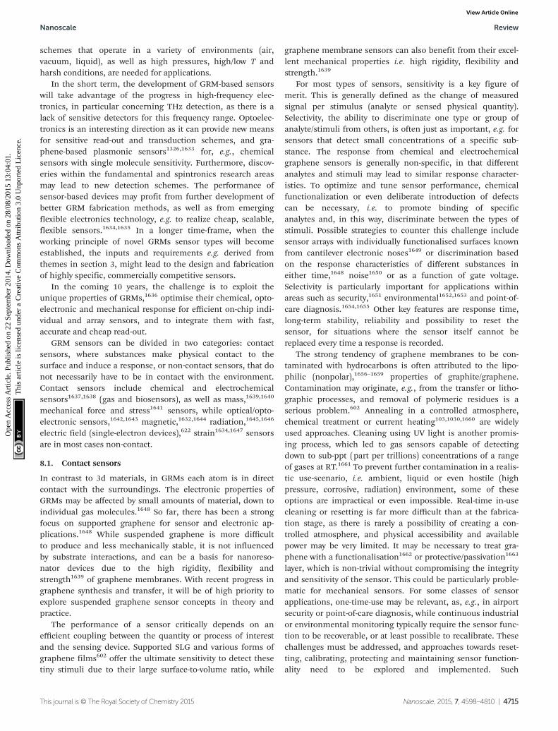
schemes that operate in a variety of environments (air,vacuum, liquid), as well as high pressures, high/low T andharsh conditions, are needed for applications.
In the short term, the development of GRM-based sensorswill take advantage of the progress in high-frequency elec-tronics, in particular concerning THz detection, as there is alack of sensitive detectors for this frequency range. Optoelec-tronics is an interesting direction as it can provide new meansfor sensitive read-out and transduction schemes, and gra-phene-based plasmonic sensors1326,1633 for, e.g., chemicalsensors with single molecule sensitivity. Furthermore, discov-eries within the fundamental and spintronics research areasmay lead to new detection schemes. The performance ofsensor-based devices may profit from further development ofbetter GRM fabrication methods, as well as from emergingflexible electronics technology, e.g. to realize cheap, scalable,flexible sensors.1634,1635 In a longer time-frame, when theworking principle of novel GRMs sensor types will becomeestablished, the inputs and requirements e.g. derived fromthemes in section 3, might lead to the design and fabricationof highly specific, commercially competitive sensors.
In the coming 10 years, the challenge is to exploit theunique properties of GRMs,1636 optimise their chemical, opto-electronic and mechanical response for efficient on-chip indi-vidual and array sensors, and to integrate them with fast,accurate and cheap read-out.
GRM sensors can be divided in two categories: contactsensors, where substances make physical contact to thesurface and induce a response, or non-contact sensors, that donot necessarily have to be in contact with the environment.Contact sensors include chemical and electrochemicalsensors1637,1638 (gas and biosensors), as well as mass,1639,1640
mechanical force and stress1641 sensors, while optical/opto-electronic sensors,1642,1643 magnetic,1632,1644 radiation,1645,1646
electric field (single-electron devices),622 strain1634,1647 sensorsare in most cases non-contact.
8.1. Contact sensors
In contrast to 3d materials, in GRMs each atom is in directcontact with the surroundings. The electronic properties ofGRMs may be affected by small amounts of material, down toindividual gas molecules.1648 So far, there has been a strongfocus on supported graphene for sensor and electronic ap-plications.1648 While suspended graphene is more difficultto produce and less mechanically stable, it is not influencedby substrate interactions, and can be a basis for nanoreso-nator devices due to the high rigidity, flexibility andstrength1639 of graphene membranes. With recent progress ingraphene synthesis and transfer, it will be of high priority toexplore suspended graphene sensor concepts in theory andpractice.
The performance of a sensor critically depends on anefficient coupling between the quantity or process of interestand the sensing device. Supported SLG and various forms ofgraphene films602 offer the ultimate sensitivity to detect thesetiny stimuli due to their large surface-to-volume ratio, while
graphene membrane sensors can also benefit from their excel-lent mechanical properties i.e. high rigidity, flexibility andstrength.1639
For most types of sensors, sensitivity is a key figure ofmerit. This is generally defined as the change of measuredsignal per stimulus (analyte or sensed physical quantity).Selectivity, the ability to discriminate one type or group ofanalyte/stimuli from others, is often just as important, e.g. forsensors that detect small concentrations of a specific sub-stance. The response from chemical and electrochemicalgraphene sensors is generally non-specific, in that differentanalytes and stimuli may lead to similar response character-istics. To optimize and tune sensor performance, chemicalfunctionalization or even deliberate introduction of defectscan be necessary, i.e. to promote binding of specificanalytes and, in this way, discriminate between the types ofstimuli. Possible strategies to counter this challenge includesensor arrays with individually functionalised surfaces knownfrom cantilever electronic noses1649 or discrimination basedon the response characteristics of different substances ineither time,1648 noise1650 or as a function of gate voltage.Selectivity is particularly important for applications withinareas such as security,1651 environmental1652,1653 and point-of-care diagnosis.1654,1655 Other key features are response time,long-term stability, reliability and possibility to reset thesensor, for situations where the sensor itself cannot bereplaced every time a response is recorded.
The strong tendency of graphene membranes to be con-taminated with hydrocarbons is often attributed to the lipo-philic (nonpolar),1656–1659 properties of graphite/graphene.Contamination may originate, e.g., from the transfer or litho-graphic processes, and removal of polymeric residues is aserious problem.602 Annealing in a controlled atmosphere,chemical treatment or current heating103,1030,1660 are widelyused approaches. Cleaning using UV light is another promis-ing process, which led to gas sensors capable of detectingdown to sub-ppt (part per trillions) concentrations of a rangeof gases at RT.1661 To prevent further contamination in a realis-tic use-scenario, i.e. ambient, liquid or even hostile (highpressure, corrosive, radiation) environment, some of theseoptions are impractical or even impossible. Real-time in-usecleaning or resetting is far more difficult than at the fabrica-tion stage, as there is rarely a possibility of creating a con-trolled atmosphere, and physical accessibility and availablepower may be very limited. It may be necessary to treat gra-phene with a functionalisation1662 or protective/passivation1663
layer, which is non-trivial without compromising the integrityand sensitivity of the sensor. This could be particularly proble-matic for mechanical sensors. For some classes of sensorapplications, one-time-use may be relevant, as, e.g., in airportsecurity or point-of-care diagnosis, while continuous industrialor environmental monitoring typically require the sensor func-tion to be recoverable, or at least possible to recalibrate. Thesechallenges must be addressed, and approaches towards reset-ting, calibrating, protecting and maintaining sensor function-ality need to be explored and implemented. Such
Nanoscale Review
This journal is © The Royal Society of Chemistry 2015 Nanoscale, 2015, 7, 4598–4810 | 4715
Ope
n A
cces
s A
rtic
le. P
ublis
hed
on 2
2 Se
ptem
ber
2014
. Dow
nloa
ded
on 2
8/08
/201
5 13
:04:
01.
Thi
s ar
ticle
is li
cens
ed u
nder
a C
reat
ive
Com
mon
s A
ttrib
utio
n 3.
0 U
npor
ted
Lic
ence
.View Article Online

considerations may also be relevant for non-contact sensors,although these are generally easier to protect.
8.1.1. Nanoelectromechanical sensors. Suspended gra-phene is the ultimate membrane, and the steadily improvingcontrol over N6, GB,1664 defects,870 large-area growth, andtransfer1665 implies that the quality and availability of suchstructures will make graphene membranes increasingly rele-vant, not just in terms of improving existing state-of-the-artsensor technology with better performance or cheaper price,but in making radically new sensor concepts possible. Nano-electromechanical (NEM) mass sensing is a viable route forhigh performance devices.1661 Mass sensing involves monitor-ing the shift of the mechanical resonance frequency of a reso-nating mechanical structure, as the mass is increased byadsorption of the particles onto the resonator,1666 Fig. 85.
The surface area-to-mass ratio of a graphene is very high(∼2630 m2 g−1),1667 hence even a molecular level of depositedmaterial on a micro- or nanosize graphene membrane can con-stitute a measurable fraction of the total mass. Mass sensorsbased on graphene membranes were predicted to approach amass resolution of 10−6 femtograms.1668 Although strong andflexible, graphene is nevertheless difficult to handle due to itsextreme thinness.1659 Suspended graphene can be fabricatedeither by transferring CVD graphene onto a structure contain-ing gaps, cavities or trenches,987,1669 by partial sacrificial etch-ing in hydrofluoric acid of the SiO2 layer on which graphene issupported,144,145 or by mechanical exfoliation of graphenedirectly on trenches,1659 which is an un-scalable process.
For commercial purposes, graphene resonators are morepromising than CNTs, since large-scale arrays with consistentdimensions are easier to produce1669 using top down micro-fabrication.1669 Graphene resonators may also benefit from alarger surface area, increasing the chance of interaction withthe analytes. As each resonator will typically have a small
capture area in order to obtain a high resonance frequency,large arrays of resonators can be a route to higher sensitivityand response rate, as well as higher spatial resolution.
One challenge for graphene membrane sensors is toachieve a sufficiently high Q-factor (quality factor) as broaden-ing of the resonance peak will reduce the mass sensitivityaccordingly. The Q-factor is the time-averaged energy stored ina resonator relative to the energy dissipated to the environ-ment per cycle,1670 and is thus decreased by dissipative losseswhere the membrane is clamped, surface effects1671 and, innon-vacuum environments, also by viscous damping.1670,1671
While the Q-factor relative to thickness can be extremely high(∼1014 m−1 (ref. 1677)) for SLG membranes, the Q-factor itselfis modest.1670 The highest reported values to date are ∼103 atRT1670 and ∼104–105 at cryogenic T.1670,1677 As the Q-factor of amembrane is inversely proportional to the surface-to-volumearea Sv,
1670 the product Sv·Q is a good indicator of the perform-ance. A graphene resonator with Sv·Q = 14 000 nm−1 was re-ported,1670 compared to Sv·Q = 100 000 nm−1 for large SiNmembranes.1670 Another figure-of-merit is the frequency-Q product. As sizes shrink, the frequency increases, while theQ-factor decreases.1650 Graphene resonators1672 reached fre-quency-Q products ∼1013, comparable to Si MEMS bulkresonators.1672
Strategies for improving the Q-factor include pre-stressingthe graphene membranes, as well as clamping them on allsides to avoid dissipation caused by edge modes.1673 Whilestudies of such nanodrums have so far shown resonancefrequency in the MHz range,1640 the GHz range should be poss-ible to reach1674 (see Fig. 86) by downscaling the resonators.
While tensile stress can directly improve the Q-factor, free-hanging graphene often suffers from slack after fabrication,e.g. caused by thermal expansion mismatch during T vari-ations, e.g. after cleaning by thermal annealing. This can be
Fig. 85 Graphene NEM structures. (a) illustration of a resonating beam of graphene connected to two electrodes. (b) graphene microribbon fabri-cated by etching the SiO2 support.1677 (c) Possible realisation of NEM spectrometer based on fully clamped graphene. By measuring the non-linearresponse from electrostatic actuation of the vibration modes, the mass and position of a particle can be determined.1678 (d) Measured and modelledtopology of stressed graphene resonator. The eigenmodes of the graphene sheet measured using AFM are compared to finite elementcalculations.1679
Review Nanoscale
4716 | Nanoscale, 2015, 7, 4598–4810 This journal is © The Royal Society of Chemistry 2015
Ope
n A
cces
s A
rtic
le. P
ublis
hed
on 2
2 Se
ptem
ber
2014
. Dow
nloa
ded
on 2
8/08
/201
5 13
:04:
01.
Thi
s ar
ticle
is li
cens
ed u
nder
a C
reat
ive
Com
mon
s A
ttrib
utio
n 3.
0 U
npor
ted
Lic
ence
.View Article Online

counteracted by clamping to a polymer that shrinks drasticallywith T,1675 which was shown to increase the Q-factor to 7000for a 10 µm beam.1675 In practical applications, particularly inliquid environments, ultrathin, large-area membrane resona-tors will be highly susceptible to viscous damping.1676 Repro-ducible and predictable wafer-level fabrication with largesingle crystalline grain sizes and a high cleanliness will be anecessary foundation for the development of effective gra-phene membrane sensors. Further research in device geome-tries to reduce losses, to control the tensile stress and toimprove long-term stability is required as well.
Modelling is also crucial. Along with the Q-factor, thephase noise (random fluctuations in the phase)1650 is usually alimiting parameter for obtaining a high mass sensitivity.1666
The main goal is to understand the impact of thermal fluctu-ations, both mechanical and electronic, on the Q-factor ofresonators and on the noise. In addition to detecting a fre-quency shift due to an adsorbed mass, it is also importantto consider the effect of particles on the local mechanicalproperties. Another aspect to be studied is how the oftenstrongly nonlinear resonant response of graphene resonatorscan be used for achieving higher sensitivity in mass-sensing,1680 Fig. 85.
Although sensor applications often take place at RT orhigher, the study of graphene resonators at low T allows abetter understanding of the fundamental limits of graphenemechanics, and this will aid in improving performance offuture. Mass sensing experiments can be pushed to extremelimits by monitoring the resonance frequency at low T.1688
Using this approach will eventually lead to improvement andbetter understanding of RT resonator sensing devices.
Sensitive electrical techniques to read out mechanicaldeformation and motion of graphene membranes at RT need
to be developed. While thermal motion detection at RT wasachieved using optical techniques,987 such techniques are notsuitable for on-chip, CMOS compatible integration. It is thusnecessary to explore various sensitive on-chip readout tech-niques, such as Si FET charge sensors and high-Q MW (micro-wave) resonant circuits. These devices may find application inmicrophones, pressure or gas detectors.
New electromechanical transduction schemes, in whichparametric interactions will play a dominant role,1681 need tobe developed. One of the possible parametric devices is a low-noise electromechanical microwave amplifier operating at lowT, expected to reach the Heisenberg limit of lowest possibleadded noise.1672 In such a device, based on suspended gra-phene, the membrane would act both as a sensor as well thelow-noise first stage preamplifier, enhancing the signal recov-ery efficiency. In general, these mechanical amplifiers wouldrepresent a simple and efficient alternative to nonlinear am-plifiers such as Josephson amplifiers1682 and converters.Together with superconducting quantum interference device(SQUID) arrays,1683 these devices are essential for the im-plementation of highly efficient, quantum-limited homodynedetection (a method of detecting frequency-modulated radi-ation by non-linear mixing with radiation of a referencefrequency1672) at MW frequency. By using mechanicalmixing, suspended graphene devices may facilitate radiationdetection even in the difficult THz band. A further opportunityoffered by graphene-based electromechanical devices is thatthey can be easily driven into the nonlinear mechanicalregime.1640,1684,2340
One application area for which NEM mass-sensing is im-mediately suited, is monitoring of aerosol content in theenvironment, which is important both for public health as wellas for a better understanding of climate factors. This requiresthe NP’s mass and size distribution to be accurately deter-mined. While current commercial sensors can determine thedistribution of particles with sizes down to the nm scale, thereis a need for compact techniques, which can accurately andconveniently determine the distribution of particles in the10–100 nm range. With an increasing need to monitor theenvironment in urban areas as well as the importance to ensurehigh safety standards in nanotechnology, such detectors areexpected to have high commercialization potential. Since par-ticle size is the primary concern, the material selectivity is lessimportant, which will allow for a relatively fast development.
Graphene resonators also hold promise for biological andchemical analysis of very small amounts of liquid-phase solu-tions. A possible application is to analyse a blood solution bydetecting the presence of different bio-molecules. The solutioncontaining the bio-molecules may be electro-sprayed onto thesensor.1685 In order to detect as many bio-molecules as poss-ible, the wafer may be covered by a large array of resonatorswith the surface of each resonator being as large as possible.Measurements using CNT resonators1686–1688 achieved sensi-tivity down to 1 yg (1 yg = 10−24 g), due to the low mass of theresonator. For graphene, sensitivities in the zeptogram (1 zg =10−21 g) range have been estimated.1689
Fig. 86 Resonance frequency and zero-point motion measured for alarge number of top-down and bottom-up CNT and graphene nano-drum resonators. Graphene nanodrums are capable of reaching GHzresonance frequencies (adapted from ref. 1674).
Nanoscale Review
This journal is © The Royal Society of Chemistry 2015 Nanoscale, 2015, 7, 4598–4810 | 4717
Ope
n A
cces
s A
rtic
le. P
ublis
hed
on 2
2 Se
ptem
ber
2014
. Dow
nloa
ded
on 2
8/08
/201
5 13
:04:
01.
Thi
s ar
ticle
is li
cens
ed u
nder
a C
reat
ive
Com
mon
s A
ttrib
utio
n 3.
0 U
npor
ted
Lic
ence
.View Article Online

To fully exploit the potential for graphene mass-sensing, itis fundamentally important to establish proof-of principleintegration of graphene resonator arrays,1669 with commer-cially available analysis front ends. Equally important is totackle the problem of multiplexing large scale arrays and devel-oping large scale fabrication methods to yield devices withhigh quality, as well as reproducibility. To this end, there is aneed for further research ranging from graphene resonatorreadout and resonator fabrication to studies aimed at obtain-ing an understanding of how the interactions between gra-phene and NPs affects performance. Also, research on howto optimize graphene resonator properties, such as Q-factorand resonance frequency is important. If successful, the useof graphene resonators as detectors in spectrometric toolswill provide a commercially sustainable means for NP de-tection, filling a missing gap in a critically important sizerange.
8.1.2. Chemical sensors. In part due to the extensiveresearch previously carried out on CNT-based chemical andelectrochemical sensors,1690,1691 graphene has potential tobecome a viable chemical sensor technology, offering highersensitivity and device integration opportunities compared toCNTs. CNT chemical sensor development is inhibited by theintrinsic heterogeneity of SWNTs ensembles.1692 Althoughnumerous approaches address the separation of s- from m-SWNTs,650–652,1006,1693–1695 further improvement is needed tosolve this in a way that is practical in a commercial scen-ario.1658 While blends of m- and s-SWNTs can be statisticallyconsistent and have a potential for sensing, recent attentionturned to GRMs.
Ref. 1648 used a Hall bar graphene device, with the chargedensity in the graphene tuned to its lowest possible level tominimise electrical noise. This allowed detection of elemen-tary charge adsorption events,1648 corresponding to individualgas molecules. Ref. 1648 estimated a detection limit in theppb range, comparable to existing sensor technologies, anddetection of gas molecules concentration in the sub ppt rangehas since been observed.1661 Graphene could become animportant chemical sensor technology not just in terms of sen-sitivity, but also price. Compact devices may be fabricated inlarge areas, on rigid as well as flexible1696,1697 substrates,which greatly enhances the practical applicability compared toconventional solid state sensors.
Substantial efforts were done to relate the adsorption pro-cesses to the observed change in conductivity.1698 As the con-ductivity is proportional to both carrier concentration and μ,σ = neμ, it can be difficult to determine which, if not both, ofthese are affected by a specific adsorption process, i.e. whetherthe dominating process is a doping or a scattering effect. Ref.1648 reported sign reversal of the conductivity change depend-ing on the adsorbent being a donor or an acceptor (seeFig. 87), however, with minimal change in μ, as confirmed byothers.1699 Numerous reports found μ improvement uponcleaning graphene from adsorbents.1700–1702 A better under-standing of the adsorption processes and their effect on theelectrical properties of graphene is necessary.
Contamination poses a serious challenge for graphenesensors, both in terms of cleaning during fabrication and formaintaining the integrity during operation. While most gra-phene applications directly benefit from a reduction ofdefects, contamination and corrugations, this is not necess-arily the case for graphene chemical sensors. Similarly toCNTs, graphene has no dangling bonds on its surface. Thegaseous molecules of interest may not easily adsorb onto pris-tine graphene surfaces.1703 The sensitivity may thus be limitedby the chemical inertness, both by inhibiting chemicalbinding of analytes and functionalization layers.1704 A possiblesolution is the deliberate introduction of defects, which hasbeen shown to enhance the chemical sensitivity of grapheneconductivity sensors as compared to pristine graphene,1704,1705
as adsorbents predominantly bind to defects. Upon adsorp-tion, edge and line defects have a far larger effect on con-ductivity than point defects, where current pathways aroundthe defect exist.1705 While this situation may occur in othermaterials, graphene is superior due to its high σ (even whenfew carriers are present) and low noise, making even smallchanges in resistance detectable.1648
Functionalisation with molecules can improve the sensorperformance in terms of sensitivity and selectivity. DNA de-posited on a graphene chemical sensor improved responseand recovery time, with the response being specific to a certainDNA sequence,1707 see Fig. 87(c and d). Large-area nano-patterning of graphene using colloid lithography was shown tobe a viable route towards even higher sensitivities1706 (seeFig. 87b).
Functionalisation of free edges should make it possible toprecisely engineer the molecular selectivity, ultimately toidentify subtle changes in the chemical composition of speciesmoving nearby those edges. Such sensors may benefit stronglyfrom being integrated in a field effect device,1648 allowing totune the carrier density to achieve maximum response peranalyte, as well as a possibility of distinguishing moleculesbased on their field effect response or even their noise spec-trum.1708 Thus, the essential challenge for graphene chemicalsensors is to develop sensor concepts that allow for selectivityas well as sensitivity.
Mechanochemical functionalization (reaction with a liquidmedium, such as alkynes and alkenes, to functionalize e.g.,nanoparticle surfaces during their formation by mechanicalprocess, e.g. by ball milling)1709 is a possible route towardshigher tunability of graphene chemical sensors. The changesof chemical reactivity upon mechanical deformation of gra-phene or CNTs are well established,1710 and there are severalroutes to deliberate formation of curvature in graphene.1711
Ref. 1712 reported that the reduced reaction barrier of stronglycurved graphene promotes adsorption of hydrogen,33 and suchcovalent binding in turn leads to stable, atomically sharpkinks that can act as barriers for electron transport. Graphenesheets can be deposited on nanostructured substrates, anddeformed according to the surface topology. Alternativelyfolds/kinks could be introduced via thermal mismatch.1713
Such deformations could lead to a modified chemical reactiv-
Review Nanoscale
4718 | Nanoscale, 2015, 7, 4598–4810 This journal is © The Royal Society of Chemistry 2015
Ope
n A
cces
s A
rtic
le. P
ublis
hed
on 2
2 Se
ptem
ber
2014
. Dow
nloa
ded
on 2
8/08
/201
5 13
:04:
01.
Thi
s ar
ticle
is li
cens
ed u
nder
a C
reat
ive
Com
mon
s A
ttrib
utio
n 3.
0 U
npor
ted
Lic
ence
.View Article Online
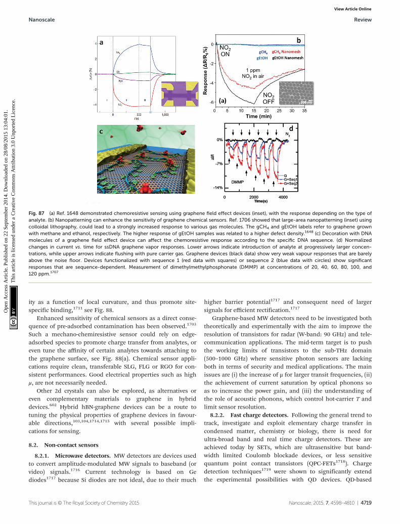
ity as a function of local curvature, and thus promote site-specific binding,1711 see Fig. 88.
Enhanced sensitivity of chemical sensors as a direct conse-quence of pre-adsorbed contamination has been observed.1703
Such a mechano-chemiresistive sensor could rely on edge-adsorbed species to promote charge transfer from analytes, oreven tune the affinity of certain analytes towards attaching tothe graphene surface, see Fig. 88(a). Chemical sensor appli-cations require clean, transferable SLG, FLG or RGO for con-sistent performances. Good electrical properties such as highμ, are not necessarily needed.
Other 2d crystals can also be explored, as alternatives oreven complementary materials to graphene in hybriddevices.602 Hybrid hBN-graphene devices can be a route totuning the physical properties of graphene devices in favour-able directions,103,104,1714,1715 with several possible impli-cations for sensing.
8.2. Non-contact sensors
8.2.1. Microwave detectors. MW detectors are devices usedto convert amplitude-modulated MW signals to baseband (orvideo) signals.1716 Current technology is based on Gediodes1717 because Si diodes are not ideal, due to their much
higher barrier potential1717 and consequent need of largersignals for efficient rectification.1717
Graphene-based MW detectors need to be investigated boththeoretically and experimentally with the aim to improve theresolution of transistors for radar (W-band: 90 GHz) and tele-communication applications. The mid-term target is to pushthe working limits of transistors to the sub-THz domain(500–1000 GHz) where sensitive photon sensors are lackingboth in terms of security and medical applications. The mainissues are (i) the increase of μ for larger transit frequencies, (ii)the achievement of current saturation by optical phonons soas to increase the power gain, and (iii) the understanding ofthe role of acoustic phonons, which control hot-carrier T andlimit sensor resolution.
8.2.2. Fast charge detectors. Following the general trend totrack, investigate and exploit elementary charge transfer incondensed matter, chemistry or biology, there is need forultra-broad band and real time charge detectors. These areachieved today by SETs, which are ultrasensitive but band-width limited Coulomb blockade devices, or less sensitivequantum point contact transistors (QPC-FETs1718). Chargedetection techniques1719 were shown to significantly extendthe experimental possibilities with QD devices. QD-based
Fig. 87 (a) Ref. 1648 demonstrated chemoresistive sensing using graphene field effect devices (inset), with the response depending on the type ofanalyte. (b) Nanopatterning can enhance the sensitivity of graphene chemical sensors. Ref. 1706 showed that large-area nanopatterning (inset) usingcolloidal lithography, could lead to a strongly increased response to various gas molecules. The gCH4 and gEtOH labels refer to graphene grownwith methane and ethanol, respectively. The higher response of gEtOH samples was related to a higher defect density.1648 (c) Decoration with DNAmolecules of a graphene field effect device can affect the chemoresistive response according to the specific DNA sequence. (d) Normalizedchanges in current vs. time for ssDNA graphene vapor responses. Lower arrows indicate introduction of analyte at progressively larger concen-trations, while upper arrows indicate flushing with pure carrier gas. Graphene devices (black data) show very weak vapour responses that are barelyabove the noise floor. Devices functionalized with sequence 1 (red data with squares) or sequence 2 (blue data with circles) show significantresponses that are sequence-dependent. Measurement of dimethylmethylphosphonate (DMMP) at concentrations of 20, 40, 60, 80, 100, and120 ppm.1707
Nanoscale Review
This journal is © The Royal Society of Chemistry 2015 Nanoscale, 2015, 7, 4598–4810 | 4719
Ope
n A
cces
s A
rtic
le. P
ublis
hed
on 2
2 Se
ptem
ber
2014
. Dow
nloa
ded
on 2
8/08
/201
5 13
:04:
01.
Thi
s ar
ticle
is li
cens
ed u
nder
a C
reat
ive
Com
mon
s A
ttrib
utio
n 3.
0 U
npor
ted
Lic
ence
.View Article Online
devices demonstrated the ability to measure very low currentand noise levels.1720
Due to the excellent gate-channel coupling and low noiseproperties, graphene nanotransistors are a promising route tooptimize the sensitivity-bandwidth product, thus paving theway to single-shot on-the-fly quantum coherent detectiondevices.
8.2.3. Strain sensors. SWNTs, depending on their chirality,show large relative resistance change (ΔR/R) per strain – ξ-(ΔL/L0, with ΔL change in length and L0, original length),
1692
the so-called gauge factor, typically ∼103, mainly due to strain-induced changes in the bandgap. Graphene is capable of with-standing very large strains without permanent mechanicaldamage (26%)1647 and without major changes in σ (6%).1647
For graphene a gauge factor of 6 was reported,1721 far fromwhat can be achieved with CNTs. CVD grown graphene trans-ferred on PDMS has shown a much higher gauge factor(∼151).1722 However, due to possible presence of defects, GBs,and possible damage to graphene in the transfer process, it isdifficult to determine the reason for the high measured gaugefactor.1722
Nevertheless, the reason why graphene is suggested as astrain sensor1634,1723 is not the sensitivity, but the high mech-anical flexibility combined with optical transparency, whichpaves the way for new applications in human-interface technol-ogy.1634 In comparison with most solid-state strain sensors,
graphene-based sensors are better suited for polymer-basedflexible electronics, displays and surfaces. Ref. 1634 demon-strated graphene-based strain sensors integrated into epoxygloves, able to read out the bending of the fingers.
It was shown theoretically1724,1725 and experi-mentally1726,1727 that a large uniaxial strain can change theelectronic properties in a way that closely resemble the effectof a large magnetic field. This pseudomagnetic field led to anexperimental observation of QHE at zero field in highlystrained graphene bubbles formed on Pt(111).1727 This effectcould be envisioned for ultra-high level pressure sensors, withthe pressure range being tuneable by adjusting the size of sus-pended graphene membranes.1726
8.2.4. Magnetic sensors. The detection of small (micro tonano Tesla) magnetic fields is a challenging issue for thedevelopment of scanning probe magnetometry,1728 biosen-sing1729 or magnetic storage.1730 Current technologies basedon giant magnetoresistance and tunnelling magnetoresistanceare limited by thermal magnetic noise and spin-torqueinstabilities.1644
Integrated Hall sensors have numerous applications,including automobiles, computers, industrial controls andconsumer devices,1731 with a ∼870 BEuro market size,1732 and90% of the market for magnetic sensors.1732 Graphene-basedHall sensors can be fabricated in a cross-shaped geometry,1731
in which the Hall effect is used to determine the magnetic
Fig. 88 Proposal for mechanochemiresistive sensor. (a) folds increase chemical reactivity, allowing (b) localised binding of atoms or molecules,eventually leading to formation of atomically sharp kinks. (c) A fold pinned by a surface structure. (d) Atoms self-aligning on a kink. (e) Kink functio-nalisation to focus analytes, or to manipulate the sensitivity/selectivity of a chemoresistive sensor. (f ) Reaction barrier at different positions of acurved graphene sheet.1712 (h) A line of hydrogen atoms in a place of high curvature could lead to a kink with an angle of 45–50°, and (i) electronictransmission through a single kink normalised by the transmission of pristine graphene (T0) as a function of the kink angle, φ, for electrons (E > 0)and holes (E < 0). The arrow indicates the normalised transmission at the equilibrium angle determined from the total energy calculations shownin h.1712
Review Nanoscale
4720 | Nanoscale, 2015, 7, 4598–4810 This journal is © The Royal Society of Chemistry 2015
Ope
n A
cces
s A
rtic
le. P
ublis
hed
on 2
2 Se
ptem
ber
2014
. Dow
nloa
ded
on 2
8/08
/201
5 13
:04:
01.
Thi
s ar
ticle
is li
cens
ed u
nder
a C
reat
ive
Com
mon
s A
ttrib
utio
n 3.
0 U
npor
ted
Lic
ence
.View Article Online
field. Such sensors might be used to measure small magneticparticles, or be made into a scanning probe to map magneticfields with a high spatial resolution.
Graphene, due to its low Hall coefficient RH = 0.3 × 10⁻⁶
Ωm T−1 [ref. 146] compared to RH = 4.3 × 10⁻⁶ Ωm T−1 forInAs,1632 is not an obvious candidate as Hall device material.However, performance comparable to existing Hall sensorswas reported using CVD-graphene.1733 Magnetic sensors basedon spintronics1632 and extraordinary magnetoresistance (EMR,i.e. very large magnetoresistance enhancement in compositemetallic and semiconducting devices)127 may be routes tohigher sensitivity. Ref. 1644, 1734 demonstrated a highly sensi-tive tuneable magnetic sensor based on a combination of theHall and EMR effects. In terms of the tunable EMR magneticsensor demonstrated by ref. 908, a high μ, as well as lowercarrier density could provide a larger Hall resistivity relative todiagonal resistivity. Graphene in BN/SLG/BN multilayers908
can satisfy these two requirements, as well as offering devicesof much smaller sizes than in conventional III–V semiconduc-tor structures. The sensitivity of such a device can be furtherimproved.1735 Having an active sensing layer thickness ofatomic dimensions located at the device surface, combinedwith the ability to electrostatically tune the device’s character-istics, paves the way towards magnetic field sensors capableof submicron spatial resolution, and tolerant to fabricationvariations.
Further theoretical predictions of novel magnetic fieldsensors based on a graphene spin capacitors were reported,1736
suggesting the use of a GNR on top of an insulator connectedto a ferromagnetic source/drain (with promising scalabilityand integration in current electronics). The large non-localspin current near the Dirac point shows that graphene may beused in spintronics without need of ferromagnetic materials toinject spin currents. This concept was demonstrated in a gra-phene-based spin capacitor.1736,1737 The time evolution of spinpolarized electrons injected into the capacitor can then beexploited as a measure of external magnetic fields at RT. Witha 100 ns spin relaxation time, magnetic fields ∼10 mOe maybe detected,1736 the measurement accuracy depending on bothdensity of magnetic defects and spin relaxation time.
Others explored the use of graphene SETs as a spin sensorsfor magnetic adsorbates,1738 to account for the experimentalhysteresis in the linear magnetoconductance of gated gra-phene nanoconstrictions, operating in the Coulomb blockaderegime. This behaviour was observed in two situations: whenmolecular magnets were deposited on graphene or CNTs,1739
and for bare graphene nanojunctions.225,715,1740
The possible bio-compatibility of supported graphene indi-cated by several cell proliferation studies1741,1742 and theenhanced sensitivity due to proximity of the graphene mag-netic sensor to biological elements could be exploited in bio-technology research and applications.1743 Arrays of Hall nano-probes for the detections of magnetic NPs may work as mag-netic markers in biomolecules. Hall nanoprobes may also beused as non-invasive heads in scanning magnetic probes. Forlow T applications, combination of graphene with supercon-
ductors may lead to quantum interference devices withextreme sensitivity to magnetic flux.1744 These may also beused to probe neural activity1745 in combination with otherGFET biosensors.
8.2.5. Signal processing in ballistic graphene-baseddevices. The similarity of electrons in graphene to relativisticDirac particles, in some cases makes a p–n junction transpar-ent for electrons arriving at normal incidence.140,141 Moreover,in ballistic p–n junctions, electrons experience focusing by then–p interface,143 which offers a new way to process signals inballistic graphene devices, by controlling electrostatically howelectrons injected by one probe focus on another (Fig. 89).While this device has relevance for electronics, the interactionbetween ballistic electrons and external stimuli such as mole-cules or light could lead to entirely new sensor concepts.
8.3. 2d crystals and hybrids
Several other LMs are relevant for 2d sensor technology, bothin enhancing the performance of the sensor layer and assensing elements.
Inorganic 2d crystals offer a range of properties relevant forsensors. Among these, MoS2 appears particularly suited due toits availability and electronic properties. Chemical sensors1746
have been fabricated from single and multi-layers MoS2,taking advantage of the semiconducting properties.
An example of a highly useful complementary material ish-BN, which is atomically flat and, unlike SiO2 and Si3N4, canbe fabricated without charge traps and corrugations.1747 Gra-phene deposited on or stacked with h-BN is mechanicallystabilized while experiencing little interference from substrateinteractions, leading to very high μ.1747,1748
8.3.1. Chemical sensors. MoS2 was used for gas sensing asearly as 1996,1749 where devices based on thin films from sus-pensions with deposited Pt-catalysts showed both high selecti-vity and sensitivity towards hydrogen. More recently, theemergence of high yield fabrication processes1750 and progressin single-layer device fabrication pushed by graphene-relatedresearch, has renewed the interest. Ref. 1751 used mechanicalexfoliated MoS2 to fabricate semiconducting FET devices anddemonstrated NO detection down to 0.8 ppm. Notably, theresults indicated that multilayer MoS2 exhibits both stable andhigh performance in NO detection, whereas single layer FETswere more unstable. The better performance of 2L-MoS2 field
Fig. 89 Prism-shaped focusing beam-splitter in a ballistic graphene n–p–n junction. Electrons emitted from contact B are distributed betweencontacts b and β. Adapted from ref. 143.
Nanoscale Review
This journal is © The Royal Society of Chemistry 2015 Nanoscale, 2015, 7, 4598–4810 | 4721
Ope
n A
cces
s A
rtic
le. P
ublis
hed
on 2
2 Se
ptem
ber
2014
. Dow
nloa
ded
on 2
8/08
/201
5 13
:04:
01.
Thi
s ar
ticle
is li
cens
ed u
nder
a C
reat
ive
Com
mon
s A
ttrib
utio
n 3.
0 U
npor
ted
Lic
ence
.View Article Online
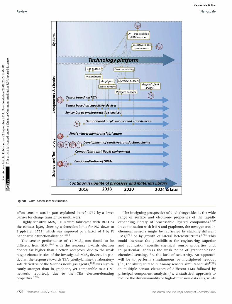
effect sensors was in part explained in ref. 1752 by a lowerbarrier for charge transfer for multilayers.
Highly sensitive MoS2 TFTs were fabricated with RGO asthe contact layer, showing a detection limit for NO down to2 ppb (ref. 1753), which was improved by a factor of 3 by Ptnanoparticle functionalization.1753
The sensor performance of 1L-MoS2 was found to bedifferent from SLG,1746 with the response towards electrondonors far higher than electron acceptors, due to the weakn-type characteristics of the investigated MoS2 devices. In par-ticular, the response towards TEA (triethylamine), a laboratory-safe derivative of the V-series nerve gas agents,1746 was signifi-cantly stronger than in graphene, yet comparable to a CNTnetwork, reportedly due to the TEA electron-donatingproperties.1746
The intriguing perspective of di-chalcogenides is the widerange of surface and electronic properties of the rapidlyexpanding library of processable layered compounds.1750
In combination with h-BN and graphene, the next-generationchemical sensors might be fabricated by stacking differentLMs,1754 or by growth of lateral heterostructures.1755 Thiscould increase the possibilities for engineering superiorand application specific chemical sensor properties and,in particular, address the weak point of graphene-basedchemical sensing, i.e. the lack of selectivity. An approachwill be to perform simultaneous or multiplexed readout(i.e., the ability to read out many sensors simultaneously1756)in multiple sensor elements of different LMs followed byprincipal component analysis (i.e. a statistical approach toreduce the dimensionality of high-dimension data sets, while
Fig. 90 GRM-based sensors timeline.
Review Nanoscale
4722 | Nanoscale, 2015, 7, 4598–4810 This journal is © The Royal Society of Chemistry 2015
Ope
n A
cces
s A
rtic
le. P
ublis
hed
on 2
2 Se
ptem
ber
2014
. Dow
nloa
ded
on 2
8/08
/201
5 13
:04:
01.
Thi
s ar
ticle
is li
cens
ed u
nder
a C
reat
ive
Com
mon
s A
ttrib
utio
n 3.
0 U
npor
ted
Lic
ence
.View Article Online
retaining most of the important variations1757). In thecontext of sensors, analytes that trigger different responsesfrom multiple sensor elements are identified according totheir response profile, rather than their multiple responseto any individual sensor. Such an approach could lead to ahigher selectivity and versatility of graphene chemicalsensing devices. A key element in optimizing sensor perform-ance will be to study the analyte–sensor interactions in detailand to identity the dominating response mechanism for thevarious LMs.
Sample fabrication and basic testing: Supported as well assuspended graphene membranes of different shapes and geo-metries of high quality and constancy must be fabricated.These will be single- and multi-layer depending onapplication.
Metal electrodes with properties to match diverse functions,such as source-drain contacts, top or bottom gate contacts oractuation/detection must be developed. Issues such as T stabi-lity, mechanical stability, contact resistance and doping/band-bending must be addressed, depending on application anduse scenario. Basic mechanical and gate-dependent electricalproperties of the devices need to be measured. The develop-ment of procedures for clean, low-damage transfer, cleaningand functionalisation/passivation must also be pursued.Strategies for enhancement or modification of chemicalsensor sensitivity/selectivity also need to be developed, basedon nanopatterning, defect engineering or molecularfunctionalisation.
Demonstration of sensor working principles: the detectionmethods need to be pushed to the limits, to achieve thehighest possible sensitivity and selectivity without sacrificingrobustness and predictability. For nanomechanical masssensors in particular, methods for on-chip actuation and posi-tion detection should be developed. Modelling of the com-bined mechanical and electrical properties will play animportant role. The aim is to develop single chips with inte-grated actuation, sensing and readout elements.
Technology and feasibility assessment supported by modelling:The suitability of the developed detection methods for use inindustrial applications needs to be assessed. In addition,sensors will benefit from the developments in other fields toidentify new applications (magnetic field sensors-based, orchemical FETs).
Important aspects to be considered are (i) size and costreduction by using graphene as sensing elements, as it willincrease the attractiveness of integrating multiple sensors withreadout and actuation electronics in the same advanced CMOSchip and (ii) use of established or nearly established industrialprocess methods, such that the proof-of-concept devices maybe industrialized as soon as industrial graphene-on-Si fabrica-tion tools enter the market.
The timeline of GRM sensors is shown in Fig. 90 and themain targets are: 3 years: Single layer membranes. Gassensors. Displacement detection with resonance amplitudesof 10 pm. Force sensitivity 520 zN/(Hz)0.5, microphone witha diameter of 600 μm with a sensitivity of 1 nm Pa−1.
Single-molecule sequencing technologies such as those usingprotein pores. 3–7 years: Mass, chemical and pressure sensors.7–10 years: Magnetic field sensors. On-chip scalable GRMsensors.
9. Flexible electronics
Flexible electronics is the next ubiquitous platform for theelectronics industry.1758 The realization of electronics with per-formance equal to that of established technologies based onrigid platforms, but in lightweight, foldable, and flexibleformats, would enable many new applications. This will bringtruly conformal, reliable or even transparent electronic appli-cations. It is also essential for rigid ultra-compact devices withtight assembly of components. It can also mean reduced costand large electronic system integration by using novel massmanufacturing approaches, such as printed electronics, R2Ror lamination, hitherto unavailable from more traditionalbrittle material and device platforms.
Flexibility will not only permit new form factors, conformalsystems and “wow effect” for consumer electronics, but willalso improve reliability and create new kinds of electricalsystems.1 Smaller, thinner and flexible electronicdevices1758,1759 could be embedded to our world (or even intous) in a new fashion. E.g., enhanced flexible electronics solu-tions may deliver miniaturised, low cost and disposablesensors integrated in transparent and flexible surfaces. Thiswould enable ubiquitous and energy autonomous sensors forthe long awaited realisation of the internet-of-things1760 andeverything-connected1761 sensor web, with application to smarthomes, industrial processes, environmental monitoring, per-sonal healthcare and more.
While a clear market pull exists and advantages of flexibleand printed electronics are clear, the true revolution is still tocome due to a number of technological challenges. First, com-mercial flexible electronics should be mechanically and electri-cally robust. Second, all used materials and componentsshould meet essential performance criteria, such as low resis-tivity or transparency, even under mechanical deformation.Furthermore, materials should be environmentally acceptable.A full industrial and market adoption will also require that theplatform allows integration of multiple technologies includingactive components. These requirements are impossible tocombine with any existing high-throughput, low-cost mass-manufacturing solution. Graphene might lead to a flexiblerevolution, and graphene-based solutions might deliverbenefits in terms of both cost advantage and uniqueness ofattributes and performance.
As a thin flexible ultra-strong film1762 and an extremelygood conductor, graphene is a natural choice also for flexible(and possibly transparent) electronic systems. It has severalunique electrical, mechanical and optical properties, whichmight enable novel unforeseen applications as well asenhanced performance. Thanks to its intrinsic flexibility, gra-phene is ideal for sensors and devices that shall adhere and
Nanoscale Review
This journal is © The Royal Society of Chemistry 2015 Nanoscale, 2015, 7, 4598–4810 | 4723
Ope
n A
cces
s A
rtic
le. P
ublis
hed
on 2
2 Se
ptem
ber
2014
. Dow
nloa
ded
on 2
8/08
/201
5 13
:04:
01.
Thi
s ar
ticle
is li
cens
ed u
nder
a C
reat
ive
Com
mon
s A
ttrib
utio
n 3.
0 U
npor
ted
Lic
ence
.View Article Online
interact with the human body, enabling new consumer andmedical applications not allowed by present technology.
Furthermore, other 2d crystals such as BN and TMDs, andheterostructures formed by their combinations can comp-lement graphene technology. The development of such a newclass of materials will further augment the impact on flexibleelectronics, by providing more functionalities and enablingnew applications.
9.1. Key technology enablers
In order to enable the realisation of flexible electronics andoptoelectronics, graphene technology should target thedevelopment of the core constituents of this new area: flexibleelectrodes (including all passive elements, such as inter-connects and antennas), and flexible active devices (includingRF transistors, sensors and LEDs). Also, transparency will be akey feature to achieve the fully deformable versions of variousdevices, such as light emitting diodes and touch panels.The combination of flexibility, electrical conductivity andtransparency makes graphene technology potentially able toovercome the main issues related to various materials testedso far as TCs, such as ITO,1763 fluorine-doped Tin oxide(FTO)1764 and others, see section 9.2.1.
Graphene-based electrodes, obtained either from inks orCVD films, may become available at a large scale, complyingwith various requirements in terms of σ and Tr, according tothe different applications. E.g., for capacitive touch panels, Rsof a few hundreds Ω □−1 would be acceptable,10 whereas lessthan 50 Ω □−1 are needed for electrodes in solar cells10 andOLEDs.10 While transparency is also required for these appli-cations, in other cases only a very low resistivity should be tar-geted. E.g., flexible antennas require flexible graphene filmswith resistivity less than 1–5 Ω □−1,1765 in order to achieveacceptable performance at ∼2–3 GHz.1765
The integration of graphene electrodes within active deviceswill require a proper engineering of the graphene work func-tion, in order to achieve ohmic contacts and low contact resist-ance with other materials. In particular, graphene electrodeswill be an advantageous choice in organic FETs, due to the lowcontact resistance achievable with organic materials.1766 E.g.,graphene provides low resistive contacts to pentacene wherethe current across these interfaces can be accurately modelledby a combination of thermionic and Poole–Frenkel emis-sion.1767 In other cases, the graphene work function will needto be tuned, e.g. by doping or chemical functionalisation. Ingeneral, this will be a major advantage and opportunity withrespect to ITO or other candidates for making flexible electro-des, whose work function can hardly be altered after the filmdeposition.1768
Graphene can act not only as a flexible electrode but, insome cases, also as an active component within a flexibledevice. E.g., graphene-based transducers can be implementedin flexible phototransistors or ChemFET (i.e. field-effectdevices where the channel conductivity is tuned by adsorptionof molecules1769,1770), exploiting both the material’s sensitivityand form factor. High μ graphene channels may be used to
enable flexible high frequency transistors. Also in this case, akey point will be the achievement of a suitable integration withthe electrodes materials, in order to minimize the contactresistance.
In order to enable the practical realisation of graphene-based products, the full supply chain needs to be covered,from basic materials – such as inks and graphene substrates –to component development and finally to a full/complete flex-ible system integration and testing.
Therefore, the graphene-based flexible electronics activityshould focus on the development of several key technologyenablers, which also reflect the development of flexible electro-des and flexible active elements within key application areas:
Materials, fabrication and integration processes: Differentfabrication approaches for graphene-based flexible electronicsneed to be studied, such as transfer and printing. The develop-ment of controlled and stable doping processes will bemandatory to achieve the required values of conductivity andcontact resistance in all devices. Also, chemical functionali-zation processes will be needed in order to allow work func-tion engineering and to control the interaction of graphenewith flexible substrates such as Polyethylene terephthalate(PET), Polyethylene naphthalate (PEN), etc.
Integrating different graphene-based technologies: integrationof flexible and rigid components, and 3d integration tech-niques all pose crucial challenges that have to be investigateddeeply, with a special focus on scaling up the manufacturingof integrated components and hardware modules. The pro-duction of graphene in large wafer scale needs to beaddressed, which would pave the way for high-speed circuits.Under most circumstances, graphene matches or exceeds μand Tr of conventional materials, though Rs has proven some-what less predictable and varies depending on productionmethod, with CVD being the closest to optimal for solar andoptoelectronics (highest Tr and lowest Rs) applications. On theother hand, printed electronics will be a major contributingfactor in low cost high yield devices in daily applications.Hence, formulation of transparent conductive inks suitable forhigh-speed inkjet printing will be crucial for large scale manu-facturing, together with the reliable production and transfer ofhomogeneous CVD graphene on a very large area.
Flexible energy solutions: Flexibility is also useful for energy-related technologies, such as energy storage and harvesting.Graphene-based electrodes could enable both large energydensity and energy capacity in fully flexible energy storagedevices, if low resistance and high surface area is achieved.Research topics include flexible batteries, super-capacitors andhybrid batteries-supercapacitors, as well as an expansion oftheir fabrication techniques to ink-jet printing, with its rapid,high volume R2R manufacturability. Graphene-based printableenergy devices (see Fig. 91) are promising1771 and should befurther developed.
Flexible RF electronics and wireless connectivity solutions:Flexibility also creates new requirements for dedicated connec-tivity, such as RF interconnects and radio communicationdevices. Current flexible transistors have unity-current-gain fre-
Review Nanoscale
4724 | Nanoscale, 2015, 7, 4598–4810 This journal is © The Royal Society of Chemistry 2015
Ope
n A
cces
s A
rtic
le. P
ublis
hed
on 2
2 Se
ptem
ber
2014
. Dow
nloa
ded
on 2
8/08
/201
5 13
:04:
01.
Thi
s ar
ticle
is li
cens
ed u
nder
a C
reat
ive
Com
mon
s A
ttrib
utio
n 3.
0 U
npor
ted
Lic
ence
.View Article Online
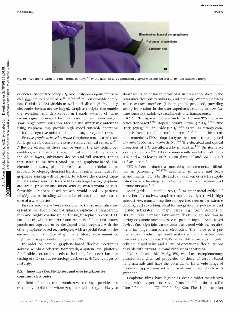
quencies, cut-off frequency – fT, and unity-power-gain frequen-cies, fmax, up to tens of GHz.867,867,1772,1773 Conformable anten-nas, flexible RF/EM shields as well as flexible high frequencyelectronic devices are envisaged. Graphene might also enablethe evolution and deployment in flexible systems of radiotechnologies optimised for low power consumption and/orshort range communication. Flexible and stretchable antennasusing graphene may provide high speed tuneable operationincluding cognitive radio implementation, see e.g. ref. 1774.
Flexible graphene-based sensors: Graphene may also be usedfor large area biocompatible sensors and chemical sensors.1637
A flexible version of these may be one of the key technologyenablers, as well as electromechanical and reliability tests ofindividual layers, substrates, devices and full systems. Topicsthat need to be investigated include graphene-based bio-chemical sensors, photodetectors and strain/deformationsensors. Developing chemical functionalization techniques forgraphene sensing will be pivotal to achieve the desired capa-bilities. Other sensors that could be envisaged using grapheneare strain, pressure and touch sensors, which would be con-formable. Graphene-based sensors would need to performreliably due to bending with radius of less than 100 mm incase of a wrist device.
Flexible passive electronics: Conductive transparent films areessential for flexible touch displays. Graphene is transparent,thin and highly conductive and it might replace present ITO-based TCFs, which are brittle and expensive.1775 Flexible touchpanels are expected to be developed and integrated with theother graphene-based technologies, with a special focus on theenvironmental stability of graphene films, achievement ofhigh patterning resolution, high μ and Tr.
In order to develop graphene-based flexible electronicssystems within a coherent framework, a system level platformfor flexible electronics needs to be built, for integration andtesting of the various technology enablers at different stages ofmaturity.
9.2. Innovative flexible devices and user interfaces forconsumer electronics
The field of transparent conductive coatings provides anexemplary application where graphene technology is likely to
showcase its potential in terms of disruptive innovation in theconsumer electronics industry, and not only. Wearable devicesand new user interfaces (UIs) might be produced, providingstrong innovation in the user experience, thanks to new fea-tures such as flexibility, stretchability and transparency.
9.2.1. Transparent conductive films. Current TCs are semi-conductor-based:1763 doped Indium Oxide (In2O3),
1776 ZincOxide (ZnO),1777 Tin Oxide (SnO2),
1763 as well as ternary com-pounds based on their combinations.1763,1777,1778 The domi-nant material is ITO, a doped n-type semiconductor composedof ∼90% In2O3, and ∼10% SnO2.
1763 The electrical and opticalproperties of ITO are affected by impurities.1763 Sn atoms actas n-type donors.1763 ITO is commercially available with Tr ∼80% and Rs as low as 10 Ω □−1 on glass,1777 and ∼60 − 300 Ω□−1 on PET.1778
ITO suffers limitations: processing requirements, difficul-ties in patterning,1763,1778 sensitivity to acidic and basicenvironments. ITO is brittle and can wear out or crack in appli-cations where bending is involved, such as touch screens andflexible displays.1779
Metal grids,1780 metallic NWs,1781 or other metal oxides1778
are other alternatives. Graphene combines high Tr with highconductivity, maintaining these properties even under extremebending and stretching, ideal for integration in polymeric andflexible substrates. In many cases (e.g. touch screens orOLEDs), this increases fabrication flexibility, in addition tohaving economic advantages. E.g., present liquid-crystal-baseddevices face high fabrication costs associated with the require-ment for large transparent electrodes. The move to a gra-phene-based technology could make them more viable. Newforms of graphene-based TCEs on flexible substrates for solarcells could add value and a level of operational flexibility, notpossible with current TCs and rigid glass substrates.
LMs such as h-BN, MoS2, WS2 etc., have complementaryphysical and chemical properties to those of carbon-basednanomaterials and have the potential to fill a wide range ofimportant applications either in isolation or as hybrids withgraphene.
Graphene films have higher Tr over a wider wavelengthrange with respect to CNT films,1782–1784 thin metallicfilms,1780,1781 and ITO,1763,1777 Fig. 92a. The flat absorption
Fig. 91 Graphene-based printed flexible battery.1771 Photograph of (a) as-produced graphene dispersion and (b) printed flexible battery.
Nanoscale Review
This journal is © The Royal Society of Chemistry 2015 Nanoscale, 2015, 7, 4598–4810 | 4725
Ope
n A
cces
s A
rtic
le. P
ublis
hed
on 2
2 Se
ptem
ber
2014
. Dow
nloa
ded
on 2
8/08
/201
5 13
:04:
01.
Thi
s ar
ticle
is li
cens
ed u
nder
a C
reat
ive
Com
mon
s A
ttrib
utio
n 3.
0 U
npor
ted
Lic
ence
.View Article Online
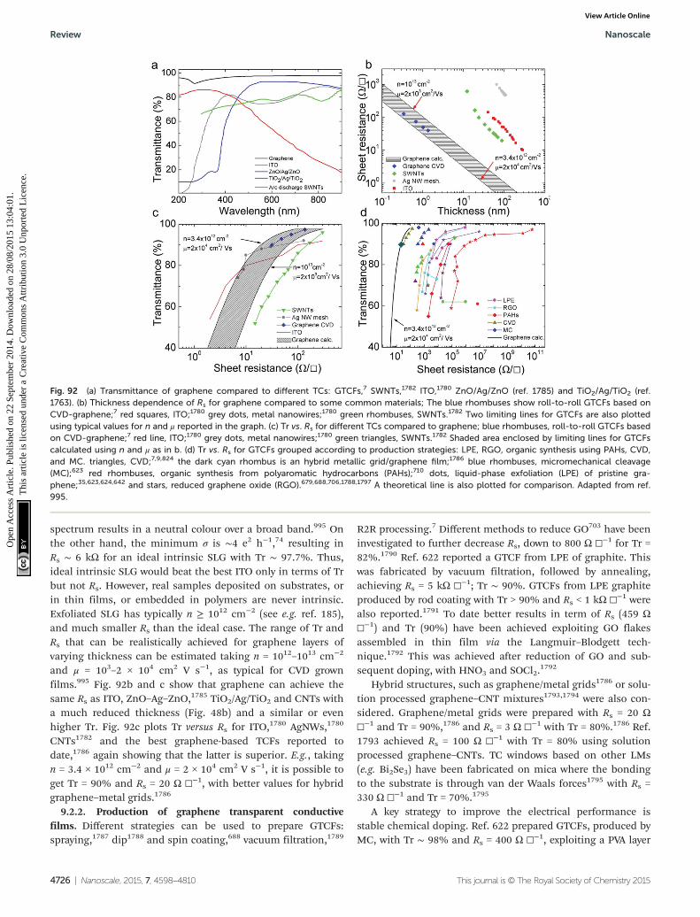
spectrum results in a neutral colour over a broad band.995 Onthe other hand, the minimum σ is ∼4 e2 h−1,74 resulting inRs ∼ 6 kΩ for an ideal intrinsic SLG with Tr ∼ 97.7%. Thus,ideal intrinsic SLG would beat the best ITO only in terms of Trbut not Rs. However, real samples deposited on substrates, orin thin films, or embedded in polymers are never intrinsic.Exfoliated SLG has typically n ≥ 1012 cm−2 (see e.g. ref. 185),and much smaller Rs than the ideal case. The range of Tr andRs that can be realistically achieved for graphene layers ofvarying thickness can be estimated taking n = 1012–1013 cm−2
and μ = 103–2 × 104 cm2 V s−1, as typical for CVD grownfilms.995 Fig. 92b and c show that graphene can achieve thesame Rs as ITO, ZnO–Ag–ZnO,
1785 TiO2/Ag/TiO2 and CNTs witha much reduced thickness (Fig. 48b) and a similar or evenhigher Tr. Fig. 92c plots Tr versus Rs for ITO,1780 AgNWs,1780
CNTs1782 and the best graphene-based TCFs reported todate,1786 again showing that the latter is superior. E.g., takingn = 3.4 × 1012 cm−2 and μ = 2 × 104 cm2 V s−1, it is possible toget Tr = 90% and Rs = 20 Ω □−1, with better values for hybridgraphene–metal grids.1786
9.2.2. Production of graphene transparent conductivefilms. Different strategies can be used to prepare GTCFs:spraying,1787 dip1788 and spin coating,688 vacuum filtration,1789
R2R processing.7 Different methods to reduce GO703 have beeninvestigated to further decrease Rs, down to 800 Ω □−1 for Tr =82%.1790 Ref. 622 reported a GTCF from LPE of graphite. Thiswas fabricated by vacuum filtration, followed by annealing,achieving Rs = 5 kΩ □−1; Tr ∼ 90%. GTCFs from LPE graphiteproduced by rod coating with Tr > 90% and Rs < 1 kΩ □−1 werealso reported.1791 To date better results in term of Rs (459 Ω□−1) and Tr (90%) have been achieved exploiting GO flakesassembled in thin film via the Langmuir–Blodgett tech-nique.1792 This was achieved after reduction of GO and sub-sequent doping, with HNO3 and SOCl2.
1792
Hybrid structures, such as graphene/metal grids1786 or solu-tion processed graphene–CNT mixtures1793,1794 were also con-sidered. Graphene/metal grids were prepared with Rs = 20 Ω□−1 and Tr = 90%,1786 and Rs = 3 Ω □−1 with Tr = 80%.1786 Ref.1793 achieved Rs = 100 Ω □−1 with Tr = 80% using solutionprocessed graphene–CNTs. TC windows based on other LMs(e.g. Bi2Se3) have been fabricated on mica where the bondingto the substrate is through van der Waals forces1795 with Rs =330 Ω □−1 and Tr = 70%.1795
A key strategy to improve the electrical performance isstable chemical doping. Ref. 622 prepared GTCFs, produced byMC, with Tr ∼ 98% and Rs = 400 Ω □−1, exploiting a PVA layer
Fig. 92 (a) Transmittance of graphene compared to different TCs: GTCFs,7 SWNTs,1782 ITO,1780 ZnO/Ag/ZnO (ref. 1785) and TiO2/Ag/TiO2 (ref.1763). (b) Thickness dependence of Rs for graphene compared to some common materials; The blue rhombuses show roll-to-roll GTCFs based onCVD-graphene;7 red squares, ITO;1780 grey dots, metal nanowires;1780 green rhombuses, SWNTs.1782 Two limiting lines for GTCFs are also plottedusing typical values for n and μ reported in the graph. (c) Tr vs. Rs for different TCs compared to graphene; blue rhombuses, roll-to-roll GTCFs basedon CVD-graphene;7 red line, ITO;1780 grey dots, metal nanowires;1780 green triangles, SWNTs.1782 Shaded area enclosed by limiting lines for GTCFscalculated using n and μ as in b. (d) Tr vs. Rs for GTCFs grouped according to production strategies: LPE, RGO, organic synthesis using PAHs, CVD,and MC. triangles, CVD;7,9,824 the dark cyan rhombus is an hybrid metallic grid/graphene film;1786 blue rhombuses, micromechanical cleavage(MC);623 red rhombuses, organic synthesis from polyaromatic hydrocarbons (PAHs);710 dots, liquid-phase exfoliation (LPE) of pristine gra-phene;35,623,624,642 and stars, reduced graphene oxide (RGO).679,688,706,1788,1797 A theoretical line is also plotted for comparison. Adapted from ref.995.
Review Nanoscale
4726 | Nanoscale, 2015, 7, 4598–4810 This journal is © The Royal Society of Chemistry 2015
Ope
n A
cces
s A
rtic
le. P
ublis
hed
on 2
2 Se
ptem
ber
2014
. Dow
nloa
ded
on 2
8/08
/201
5 13
:04:
01.
Thi
s ar
ticle
is li
cens
ed u
nder
a C
reat
ive
Com
mon
s A
ttrib
utio
n 3.
0 U
npor
ted
Lic
ence
.View Article Online
to induce n-type doping. Ref. 7 achieved Rs ∼ 30 Ω □−1; Tr ∼90% by nitric acid treatment of GTCFs derived from CVDgrown flakes, one order of magnitude lower in terms of Rsthan previous GTCFs from wet transfer of CVD films.7 Acidtreatment permitted to decrease the Rs of hybrid nanotube–graphene films to 100 Ω □−1 for Tr = 80%.1796 Fig. 92d over-views current GTCFs. It shows that GTCFs derived from CVD,combined with doping, could outperform ITO, metal wiresand SWNTs. A hybrid graphene–metallic grid has shown prom-ising results as a possible ITO alternative (Rs ∼ 20 Ω □−1; Tr ∼90%).
Note that GTCFs and GOTCFs produced by other methods,such as LPE, albeit presently with higher Rs at Tr = 90%, havealready been tested in organic light emitters,691,1790 solarcells1788 and flexible smart window.995 These are a cheaperand easier scalable alternative to CVD films, and should beconsidered in applications where cost reduction is crucial.
Increasing the carrier density by doping is a means toreduce Rs. However, in most cases the stability of the dopant isunknown. Innovative doping routes need to be investigated, inorder to achieve stable doping, preserving electrical propertiesover extended time scales. Doping simultaneous to growth canbe achieved exploiting alternative precursors (e.g. pyridine, amolecule structurally related to the benzene ring but alreadywith a donor nitrogen atom in the ring). Another route is“molecular doping” by stable hydrazil- and nitroxide- organicradicals.
Reliable transfer of large-area graphene onto arbitrary sub-strates is a critical step in the use of CVD-grown graphene. Inmany cases, the transfer process results in loss of material,and it is difficult to avoid contamination, wrinkling and break-age. Dry transfer techniques have also been developed,602 butneed to be optimized for different substrates and conditions.The presence of the substrate generally modifies graphene’selectronic properties and thus it is important to optimizeinteractions between graphene and substrate. One way is themodification of the substrate surface by applying surface treat-ments. The question is how the bonding of graphene to thevarious substrates affects the electronic properties. The vari-ations with the support can, in turn, provide additionalcontrol of the graphene properties. A deeper understandingof these phenomena should be achieved, in order to usethese effects for tailoring the chemical reactivity of supportedgraphene. For many aforementioned applications, thermalexpansion and conductivity are crucial and will need to beinvestigated and optimised. Moreover, the combination ofgraphene and related 2d crystals should lead to significantcharge redistribution at the interface. Thus, tuning ofdifferent parameters such as μ and work function should bestudied.
Another approach is to develop processed LPE graphene de-posited on a variety of flexible polymeric substrates to realizeTCFs using an up-scalable, R2R coating, with the aim ofachieving Tr ∼ 90–95%, with Rs < 100 Ω □−1 and tuneablework function. The achievement of these targets would permitthe integration of GTCFs in many applications.
Characterization methods that are compatible with largeareas will be required to monitor quality and consistency of as-produced GTCFs. Scanning probe microscopies as well as TEMare very suitable for investigation of selected regions withsmall to moderate areas, however, not practical for fastmapping of large areas. Apart from micro-Raman mappingand optical inspection, large-area mapping techniques willneed to be developed, including conductivity probes and THzprobes.
9.2.3. Mechanical performance of transparent films forflexible electronics. Static and dynamic flexing pose interest-ing questions on how devices incorporated with differenttransparent films should perform in terms of various testingconditions, such as fatigue, torsion and repetitive bendingcycles. One factor is also long-term stability of the materialinfluenced under various environmental conditions. Si tech-nology is rigid, but in recent years thinned down Si has beenused to provide flexibility1798 and reduce the strain in fabri-cated devices that can lead to failure. Graphene, mechanicallyunique due to its toughness, has very good static and dynamicflexible properties. Static and dynamic flex testing, such asthree or four point bend testing to a particular radius(∼10 mm), can lead to fracture, but the characteristics of gra-phene provide unique advantages to overcome such challengesand should enable it to sustain cyclic fatigue testing up to amillion cycles. Such characterisation will lead to industry stan-dardization for manufacturers intending to integrate variousGRMs for various applications, from touch panels to printedelectronic applications.
9.2.4. Applications of graphene transparent conductivefilms. The current GTCFs performances are very promising inview of commercial applications, already matching require-ments for many of them, see Fig. 93. Graphene can be used asa window in inorganic (Fig. 94a), organic (Fig. 94b) and DSSCs(Fig. 94c).
A uniform graphene layer can be transferred to the requiredsubstrate and large area graphene has been transferred to 30 ×30 cm2 substrates with low T lamination techniques.1799
Solar cells: The TC layer is a necessary component of allthin film solar cells and it has a major impact on efficiency,resulting in a 10–25% power loss even for the best TCs.1800 Forthe development or adoption of any new TC material, it isuseful to know the impact on efficiency and the requirementsto improve overall efficiency. Graphene can reduce losses,since it can have Tr > 90%, with Rs < 100 Ω □−1. A figure ofmerit is the ratio of DC conductivity and absorptivity (absorp-tion coefficient). This does not depend on device architectureor film thickness and can be determined from Rs andabsorption.
OLEDs: OLEDs can also take advantage of graphene.1790
They consist of an electroluminescent layer between twocharge- injecting electrodes, at least one of which transpar-ent.995 In these diodes, holes are injected into the highestoccupied molecular orbital (HOMO) of the polymer from theanode, and electrons into the lowest unoccupied molecularorbital (LUMO) from the cathode. For efficient injection, the
Nanoscale Review
This journal is © The Royal Society of Chemistry 2015 Nanoscale, 2015, 7, 4598–4810 | 4727
Ope
n A
cces
s A
rtic
le. P
ublis
hed
on 2
2 Se
ptem
ber
2014
. Dow
nloa
ded
on 2
8/08
/201
5 13
:04:
01.
Thi
s ar
ticle
is li
cens
ed u
nder
a C
reat
ive
Com
mon
s A
ttrib
utio
n 3.
0 U
npor
ted
Lic
ence
.View Article Online
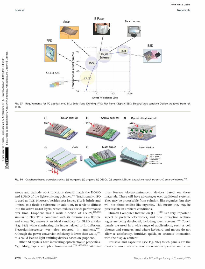
anode and cathode work functions should match the HOMOand LUMO of the light-emitting polymer.995 Traditionally, ITOis used as TCF. However, besides cost issues, ITO is brittle andlimited as a flexible substrate. In addition, In tends to diffuseinto the active OLED layers, which reduces device performanceover time. Graphene has a work function of 4.5 eV,109,995
similar to ITO. This, combined with its promise as a flexibleand cheap TC, makes it an ideal candidate for OLED anodes(Fig. 94d), while eliminating the issues related to In diffusion.Electroluminescence was also reported in graphene.1801
Although the power conversion efficiency is lower than CNTs,995
this could lead to light-emitting devices based on graphene.Other 2d crystals have interesting optoelectronic properties.
E.g., MoS2 layers are photoluminescent.378,1802,1803 We can
thus foresee electroluminescent devices based on thesematerials. These will have advantages over traditional systems.They may be processable from solution, like organics, but theywill not photo-oxidise like organics. This means they may beprocessable in ambient conditions.
Human Computer Interaction (HCI)1804 is a very importantaspect of portable electronics, and new interaction techno-logies are being developed, including touch screens.1805 Touchpanels are used in a wide range of applications, such as cellphones and cameras, and where keyboard and mouse do notallow a satisfactory, intuitive, quick, or accurate interactionwith the display content.
Resistive and capacitive (see Fig. 94e) touch panels are themost common. Resistive touch screens comprise a conductive
Fig. 93 Requirements for TC applications, SSL: Solid State Lighting; FPD: Flat Panel Display; ESD: ElectroStatic sensitive Device. Adapted from ref.1806.
Fig. 94 Graphene-based optoelectronics. (a) inorganic, (b) organic, (c) DSSCs, (d) organic LED, (e) capacitive touch screen, (f ) smart windows.995
Review Nanoscale
4728 | Nanoscale, 2015, 7, 4598–4810 This journal is © The Royal Society of Chemistry 2015
Ope
n A
cces
s A
rtic
le. P
ublis
hed
on 2
2 Se
ptem
ber
2014
. Dow
nloa
ded
on 2
8/08
/201
5 13
:04:
01.
Thi
s ar
ticle
is li
cens
ed u
nder
a C
reat
ive
Com
mon
s A
ttrib
utio
n 3.
0 U
npor
ted
Lic
ence
.View Article Online

substrate, a liquid crystal display (LCD) front panel, and aTCF.1805 When pressed by a finger or pen, the front panel filmcomes into contact with the bottom TC and the coordinates ofthe contact point are calculated on the basis of their resistancevalues. The TC requirements for resistive screens are Rs ∼ 500− 2000 Ω □−1 and Tr > 90% at 550 nm.1805 Favourable mechan-ical properties, including brittleness and wear resistance, highchemical durability, no toxicity, and low production costs arealso important. GTCFs can satisfy the requirements for resis-tive touch screens in terms of T and Rs, when combined withlarge area uniformity. Ref. 7 reported a graphene-based touchpanel by screen-printing a CVD sample. Considering the Rsand T required by analogue resistive screens, GTCF or GOTCFproduced via LPE also offer a viable alternative, and furthercost reduction.
On the other hand, capacitive touch panels are more versa-tile and work much faster than resistive panels and currentlyare used in many mainstream electronics applications.995
Capacitive touch screens are emerging as the high-end versionof touch panels. These consist of an insulator such as glass,coated with ITO.1805 As the human body is also a conductor,touching the surface of the screen results in an electrostaticfield distortion, measurable as a change in capacitance.The capacitive touch panel market is also driven by thechip vendors and manufacturers where the specification iscritical to the Rs of the material. Moreover, effective drive andsense lines routing resistance, electromagnetic interference(EMI) shielding performance, low noise performance andtransmission characteristics (Tr > 90%) are also crucialparameters.
A display is typically embedded in a touch panel, creatinginterference that must be shielded.1807 EMI shielding isusually achieved via a metal mesh structure,1808 which attenu-ates transmitting electric fields to a desired level. Importantly,an optimal shielding mesh should also be transparent, toavoid haze,1809 birefringence1809 and Moiré effects.1810 EMIshielding of RF radiation in electronic devices has become aserious concern,1807 and a very good average EMI shieldingeffectiveness, defined as1807 SE = −10 log|Tr| (dB) where Tr isthe transmittance of the shield, was reported for SLG on a flex-ible substrate.1807 In theory, SLG without defects or wrinklescan block as much as 97.8% of EMI.1807 Graphene compositescould also be used for EMI. Therefore, graphene technologymay provide new solutions for manufacturing transparent andflexible EMI shielding coatings, with impact in portable elec-tronic devices and flexible electronics.
The challenges that graphene will be facing would be the Rslevels compared to ITO and Ag. The cost would offset ITO andAg in comparison to graphene, but there needs to be somechemical modification of graphene in order to decrease Rsto below hundreds Ω □−1 from its intrinsic value while retain-ing Tr.
These touch panels solutions for HCI do not yet providefull satisfaction in terms of user experience,1811 as touchscreens tend to be inert in the way they interact with a user.Also, the proliferation of icons, virtual keys and densely
packed browsing menus on mobile touch screens requiresincreasing cognitive efforts from the user in order to locate,distinguish and manipulate them. Solutions for low-cognitiveeffort UIs,1812,1813 such as vibration enabled tactile feedback,are currently gaining momentum, and could improve usability,interaction interoperability, and user acceptance. Thus far, themost active tactile feedback solutions have been implementedthrough monolithic vibrations of the entire device driven by asingle or very few vibrating actuators, typically electromechani-cal1814 or piezoelectric.1815 The types of tactile feedback thatcan be provided by such techniques are limited to quite basicpatterns, only partially correlated to finger position, perceivedaudio-visual information and actions. Such solutions do notyet provide complete satisfaction in terms of user experience.
Key to this is the inability of monolithic vibrations toprovide localized tactile feedback associated with visualimages, and this is related to the difficulty in implementingtactile feedback directly from a display surface.1816,1817 Toaddress the problem, a flexible and optically transparent gra-phene-based programmable electrostatic tactile (ET) systemwas developed capable of delivering localized tactile infor-mation to the user’s skin, directly from the display’s surfaceand in accordance with the displayed visual information (seeFig. 95).1758 Ref. 1818 developed a transparent and stretchablegraphene-based actuator, composed of transparent and com-pliant graphene electrodes and a dielectric elastomer sub-strate, for tactile displays. The graphene electrode is coatedonto the designed region of the substrate layer by layer, thusonly the area of the dielectric elastomer substrate with electro-des bumps up in response to the input voltage, which conse-quently produces actuation.1818 Apart from being simple infabrication, cost-effective and extendible to multiple arrays,the actuator preserves its electrical and mechanical propertieseven under 25% stretching.1818
Aside these “high end” applications, TCEs are used inseveral other every-day applications, such as low-emissivitywindows in buildings,1758 electro-chromic mirrors1819 andwindows,1819 static dissipation,1819 EM shielding,1819 invisiblesecurity circuits,1819 defrosting windows,1819 oven windows.1819
Considering the diversity of applications for TCs, differentmaterials are most suitable for all uses. Depending on whichmaterial property is of most importance, different choices arepossible.1819 However, considering that the majority of these
Fig. 95 Graphene-based electrotactile display. Adapted from ref. 1758.
Nanoscale Review
This journal is © The Royal Society of Chemistry 2015 Nanoscale, 2015, 7, 4598–4810 | 4729
Ope
n A
cces
s A
rtic
le. P
ublis
hed
on 2
2 Se
ptem
ber
2014
. Dow
nloa
ded
on 2
8/08
/201
5 13
:04:
01.
Thi
s ar
ticle
is li
cens
ed u
nder
a C
reat
ive
Com
mon
s A
ttrib
utio
n 3.
0 U
npor
ted
Lic
ence
.View Article Online
applications do not require very low Rs (a Rs of a few hundredsof Ω □−1 can generally be used995) and that graphene can beproduced in many different ways with diverse properties,GTCEs are likely to impact the TCEs market. In particular,GTCFs produced by LPE are appealing in low-tech appli-cations, for ease of fabrication and low cost.
Electrically switchable optical shutters or similar structures,generally known as ‘smart windows’1820 are other devices thatcan take advantage from GTCEs. Smart windows consist ofthin films of optically transparent polymers with micron-sizedliquid crystal (LC) droplets contained within pores of thepolymer.1821–1823 Light passing through the LC/polymer isstrongly forward scattered, producing a milky film. If the LCordinary refractive index is close to that of the host polymer,the application of an electric field results in a transparentstate.1824 The ability of switching from translucent to opaquemakes them attractive in many applications, e.g. where privacyat certain times is highly desirable. There are other potentialapplications of PDLCs in flexible displays, such as an organicthin film transistor driven flexible display with each individualpixel controlled by an addressable PDLC matrix.1824 Conven-tionally, ITO on glass is used as TCF to apply the electric fieldacross the PDLC. One of the reasons behind the limitedmarket penetration of smart windows is the significant ITOcost. Furthermore, flexibility is hindered when using ITO,reducing potential applications, such as PDLC flexible dis-plays.1824 For transparent or coloured/tinted smart windows,the required Tr and Rs range from 60 to 90% and above and100 to 1 kΩ □−1, depending on production cost, applicationand manufacturer. In addition to flexibility, the electrodesneed to be as large as the window itself and must have long-term physical and chemical stability, as well as being compati-ble with R2R PDLC production process. LCs could also beused for next-generation zero-power monochromatic andcoloured flexible bi-stable displays, which can retain an imagewith no power consumption.1825 These are attractive for signsand advertisements or for e-readers, and require TCs forswitching the image. The present ITO devices are not ideal forthis application, owing to the limitations discussed above.
9.2.5. 2d crystals and hybrids for flexible electronics. Var-ious 2d crystals have already demonstrated a great potential tocomplement graphene. Some of the materials that haverecently triggered a lot of interest are h-BN and TMDs such asMoS2. BN is an insulating isomorph of graphene with excellentdielectric properties, and can be used in ultra-thin and flat gra-phene-based transistors on rigid and flexible substrates.1826
Graphene-BN heterostructures can enhance the performanceof field effect devices.1827 MoS2
1519 is suitable for applicationsin electronics on soft substrates. Since pristine graphene hasno bandgap,74 the availability of other 2d crystals is essentialfor the development of novel flexible electronic devices. Flex-ible MoS2 FET devices have been reported with ION/IOFF > 107
and μ ∼ 30 cm2 V s−1 using high-K dielectric, such ashafnium oxide.1828 Replacing the conventional dielectric (e.g.Aluminium oxide) with BN on MoS2 transistors may enableflexible and stretchable high-speed electronics and RF devices.
The combination of the properties of various 2d crystals inheterostructures will open new opportunities in many fields offlexible electronics.
Applications that might be enhanced by the development of2d crystals can be identified in the field of flexible electronics:
1. Flexible TFT and RF devices. The use of 2d crystals inhybrid 2d devices on flexible substrates (e.g. using BN as adielectric and MoS2 or WS2 as a semiconductor) may solve theproblem of the lack of a bandgap in pristine graphene for flex-ible TFTs. The combined use of atomically flat 2d dielectrics,such as BN, may enable high μ flexible transistors for highspeed flexible electronics. Also, strain engineering of thebandgap of 2d crystals1829 may offer new solutions for flexibleelectronic devices.
2. Flexible optoelectronics. Due to its direct bandgap,1L-MoS2 is a promising material for optoelectronics. Atunability of the bandgap is predicted in heterostructuresmade by stacking different 2d semiconducting crystals (e.g.MoS2 and WS2) in different ways,1830 opening the opportunityto engineer new optoelectronic materials. Therefore, novelflexible optoelectronic devices will be enabled by thedevelopment of the 2d crystals technology. Heterostructuresbased on 2d crystals have also a great potential for flexiblephotovoltaics. Light–matter interaction can be stronglyenhanced in 2d crystals heterostructures, leading to an EQE∼30%.1529
3. Flexible sensors. In the field of chemical sensors and bio-sensors, the combination of various 2d crystals and graphenederivatives may offer the opportunity to add selectivity to thehigh sensitivity typical of these all-surface materials. Arrays ofsensors made of different 2d sensing materials may be inte-grated on top of flexible substrates, and a specific response tothe analytes may be achieved via neural network approaches(e.g. “electronic nose”1831). Furthermore, flexible strain sensorsmay be developed based on the sensitivity of 2d crystals todeformation.
The main development steps toward flexible electronicdevices based on 2d crystals are:
– Materials. Suitable inks for screen and inkjet printingon flexible substrates have to be developed. A library of func-tional inks based on 2d crystals will enable flexible printeddevices, such as sensors and transistors. Large area depositionor growth processes (such as CVD) need to be developed for2d crystals, together with suitable (clean) post-processingmethods (transfer on flexible substrates, annealing). Con-trolled doping techniques have to be identified.
– Integration. Compatible processes for manufacturingintegrated hybrid graphene/2d crystals-based devices mustbe developed, together with suitable flexible substrates forthe integration of hybrid structures. A good control ofthe interfaces should be achieved in manufacturing 2dheterostructures, controlling both the coupling betweendifferent 2d crystals and the interaction with the substrate.
– Mechanical performance. In general, 2d crystals are flex-ible, but the combined use of conventional materials and elec-trodes in flexible devices can create constraints in terms of
Review Nanoscale
4730 | Nanoscale, 2015, 7, 4598–4810 This journal is © The Royal Society of Chemistry 2015
Ope
n A
cces
s A
rtic
le. P
ublis
hed
on 2
2 Se
ptem
ber
2014
. Dow
nloa
ded
on 2
8/08
/201
5 13
:04:
01.
Thi
s ar
ticle
is li
cens
ed u
nder
a C
reat
ive
Com
mon
s A
ttrib
utio
n 3.
0 U
npor
ted
Lic
ence
.View Article Online
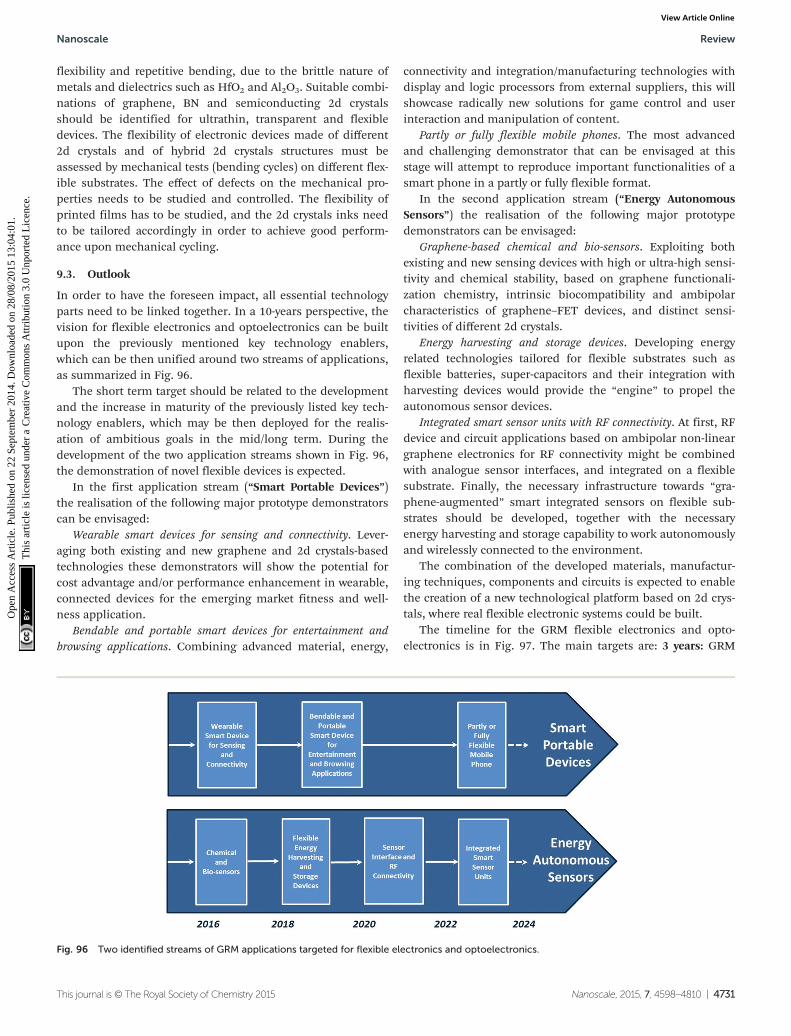
flexibility and repetitive bending, due to the brittle nature ofmetals and dielectrics such as HfO2 and Al2O3. Suitable combi-nations of graphene, BN and semiconducting 2d crystalsshould be identified for ultrathin, transparent and flexibledevices. The flexibility of electronic devices made of different2d crystals and of hybrid 2d crystals structures must beassessed by mechanical tests (bending cycles) on different flex-ible substrates. The effect of defects on the mechanical pro-perties needs to be studied and controlled. The flexibility ofprinted films has to be studied, and the 2d crystals inks needto be tailored accordingly in order to achieve good perform-ance upon mechanical cycling.
9.3. Outlook
In order to have the foreseen impact, all essential technologyparts need to be linked together. In a 10-years perspective, thevision for flexible electronics and optoelectronics can be builtupon the previously mentioned key technology enablers,which can be then unified around two streams of applications,as summarized in Fig. 96.
The short term target should be related to the developmentand the increase in maturity of the previously listed key tech-nology enablers, which may be then deployed for the realis-ation of ambitious goals in the mid/long term. During thedevelopment of the two application streams shown in Fig. 96,the demonstration of novel flexible devices is expected.
In the first application stream (“Smart Portable Devices”)the realisation of the following major prototype demonstratorscan be envisaged:
Wearable smart devices for sensing and connectivity. Lever-aging both existing and new graphene and 2d crystals-basedtechnologies these demonstrators will show the potential forcost advantage and/or performance enhancement in wearable,connected devices for the emerging market fitness and well-ness application.
Bendable and portable smart devices for entertainment andbrowsing applications. Combining advanced material, energy,
connectivity and integration/manufacturing technologies withdisplay and logic processors from external suppliers, this willshowcase radically new solutions for game control and userinteraction and manipulation of content.
Partly or fully flexible mobile phones. The most advancedand challenging demonstrator that can be envisaged at thisstage will attempt to reproduce important functionalities of asmart phone in a partly or fully flexible format.
In the second application stream (“Energy AutonomousSensors”) the realisation of the following major prototypedemonstrators can be envisaged:
Graphene-based chemical and bio-sensors. Exploiting bothexisting and new sensing devices with high or ultra-high sensi-tivity and chemical stability, based on graphene functionali-zation chemistry, intrinsic biocompatibility and ambipolarcharacteristics of graphene–FET devices, and distinct sensi-tivities of different 2d crystals.
Energy harvesting and storage devices. Developing energyrelated technologies tailored for flexible substrates such asflexible batteries, super-capacitors and their integration withharvesting devices would provide the “engine” to propel theautonomous sensor devices.
Integrated smart sensor units with RF connectivity. At first, RFdevice and circuit applications based on ambipolar non-lineargraphene electronics for RF connectivity might be combinedwith analogue sensor interfaces, and integrated on a flexiblesubstrate. Finally, the necessary infrastructure towards “gra-phene-augmented” smart integrated sensors on flexible sub-strates should be developed, together with the necessaryenergy harvesting and storage capability to work autonomouslyand wirelessly connected to the environment.
The combination of the developed materials, manufactur-ing techniques, components and circuits is expected to enablethe creation of a new technological platform based on 2d crys-tals, where real flexible electronic systems could be built.
The timeline for the GRM flexible electronics and opto-electronics is in Fig. 97. The main targets are: 3 years: GRM
Fig. 96 Two identified streams of GRM applications targeted for flexible electronics and optoelectronics.
Nanoscale Review
This journal is © The Royal Society of Chemistry 2015 Nanoscale, 2015, 7, 4598–4810 | 4731
Ope
n A
cces
s A
rtic
le. P
ublis
hed
on 2
2 Se
ptem
ber
2014
. Dow
nloa
ded
on 2
8/08
/201
5 13
:04:
01.
Thi
s ar
ticle
is li
cens
ed u
nder
a C
reat
ive
Com
mon
s A
ttrib
utio
n 3.
0 U
npor
ted
Lic
ence
.View Article Online
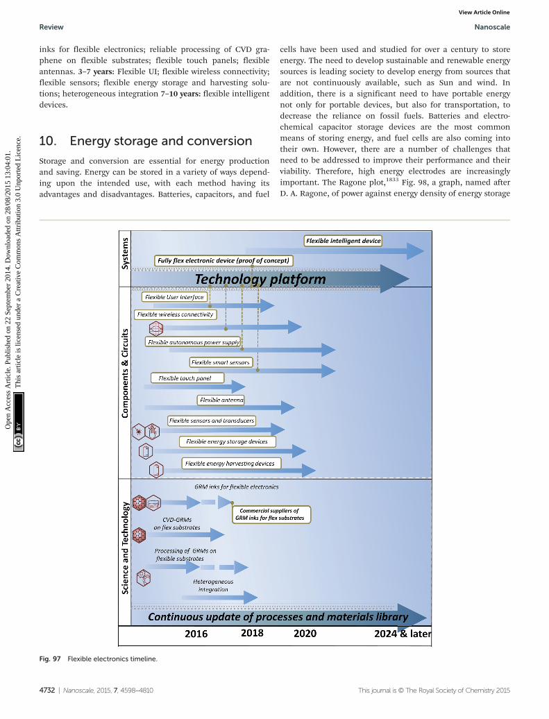
inks for flexible electronics; reliable processing of CVD gra-phene on flexible substrates; flexible touch panels; flexibleantennas. 3–7 years: Flexible UI; flexible wireless connectivity;flexible sensors; flexible energy storage and harvesting solu-tions; heterogeneous integration 7–10 years: flexible intelligentdevices.
10. Energy storage and conversion
Storage and conversion are essential for energy productionand saving. Energy can be stored in a variety of ways depend-ing upon the intended use, with each method having itsadvantages and disadvantages. Batteries, capacitors, and fuel
cells have been used and studied for over a century to storeenergy. The need to develop sustainable and renewable energysources is leading society to develop energy from sources thatare not continuously available, such as Sun and wind. Inaddition, there is a significant need to have portable energynot only for portable devices, but also for transportation, todecrease the reliance on fossil fuels. Batteries and electro-chemical capacitor storage devices are the most commonmeans of storing energy, and fuel cells are also coming intotheir own. However, there are a number of challenges thatneed to be addressed to improve their performance and theirviability. Therefore, high energy electrodes are increasinglyimportant. The Ragone plot,1833 Fig. 98, a graph, named afterD. A. Ragone, of power against energy density of energy storage
Fig. 97 Flexible electronics timeline.
Review Nanoscale
4732 | Nanoscale, 2015, 7, 4598–4810 This journal is © The Royal Society of Chemistry 2015
Ope
n A
cces
s A
rtic
le. P
ublis
hed
on 2
2 Se
ptem
ber
2014
. Dow
nloa
ded
on 2
8/08
/201
5 13
:04:
01.
Thi
s ar
ticle
is li
cens
ed u
nder
a C
reat
ive
Com
mon
s A
ttrib
utio
n 3.
0 U
npor
ted
Lic
ence
.View Article Online

devices, permits to compare different technologies and judgetheir usefulness for a particular application, e.g. when highenergy density or power density is needed.
10.1. Batteries
Many forms of storage exist, including large-scale storage suchas hydroelectric power and compressed air, as well as flywheels and electrochemical energy storage (Li-ion batteries,redox flow batteries and supercapacitors).
At present, Li-ion batteries, using the chemistry of a LiCoO2
cathode and a graphite anode,1834–1837 are considered by thebatteries community the leading candidates for hybrid, plug-in hybrid, and all electrical vehicles, and for utility appli-cations. The energy density and performance of Li-ion bat-teries largely depend on the physical and chemical propertiesof the cathode and anode materials. Conventional Li-ion bat-teries utilize graphite as the anode.1838 The low theoreticalspecific capacity (i.e. the total ampere-hours (Ah) availablewhen a battery is discharged at a defined value of dischargecurrent, per unit weight) of graphite (372 mA h g−1 [ref. 1838])makes it important to find alternative negative electrodes. Si(4200 mA h g−1)1839 or Sn (994 mA h g−1)1840 have highercapacity. However, their application as anodes in Li-ion bat-teries has been limited by their poor cycling (i.e. the numberof charge/discharge cycles before the battery fails to meetperformance criteria, e.g. specific capacity below 60% ofnominal value) caused by large volume changes during the
uptake and release of Li.1841 The search for suitable cathodeand anode materials has proven challenging. The possibilitiesfor the improvement of cathode materials are quite limiteddue to the stringent requirements, such as high voltagepotential, structural stability, and inclusion of Li in thestructure.1842,1843
Many potential electrode materials (e.g. metal oxide) inLi-ion batteries are limited by slow Li-ion diffusion1836,1837 andpoor electron transport1836,1837 at high charge/dischargerates.1836,1837 To improve the charge-discharge rate perform-ance of Li-ion batteries, extensive work focused on Li-ion and/or electron transport in electrodes.1844 Nanostructures (e.g.,nanoscale size1845 or nanoporous1846 materials) have beenwidely investigated to improve Li-ion transport in electrodes byshortening the Li-ion insertion/extraction pathway.1844,1847
A variety of approaches were developed to increaseelectron transport in the electrode materials, such as the useof conductive coatings (e.g. carbon black, CNTs1848–1850). In Li+
batteries, higher energy requires electrodes with high conduc-tivity and improved resistance to reaction with electrolytes.Graphene may be an ideal conductive additive for hybridnanostructured electrodes.1851,1852 Other advantages includehigh surface area (theoretical ∼2630 m2 g−1)1667 for improvedinterfacial contact and potential for low manufacturing cost.
High-surface-area RGO sheets were studied for Li-ionstorage.1853 In addition, RGO was used to form compositeswith SnO2 in order to improve specific capacity and cyclicstability of anodes.1854 GRMs were also used as a conductiveadditive in self-assembled hybrid nanostructures to enhancethe performance (i.e., charge/discharge capacity, and currentand energy density) of electrochemical active materials.1855,1856
However, the majority of electrodes were fabricated exploitingCMG and only recently the full potential of graphene producedby LPE was exploited622 in electrodes for Li-ion batteries. Ref.622 reported that electrodes based on Cu-supported graphenenanoflakes ink can reach specific capacities ∼1500 mA h g−1 ata current rate ∼100 mA g−1 and specific capacities ∼650 mA hg−1 at a current rate ∼700 mA g−1 over 150 cycles, when testedin half-cell configuration (i.e. with a structure that contains aconductive electrode and a surrounding conductive electrolyteseparated by a Helmholtz double layer). By balancing the cellcomposition and suppressing the initial irreversible specificcapacity of the anode (∼7500 mA h g−1), principally due to thedecomposition of the electrolyte at the surface of the electrodewith the formation of a solid electrolyte interphase (SEI),ref. 622 reported an optimal battery performance in terms ofspecific capacity, i.e. 165 mA h g−1, estimated energy density∼190 W h kg−1, operation over 80 charge-discharge cycles.
Table 6 summarizes the performances (i.e., charge/dis-charge capacity, and current and energy density) of GRM-based Li-ion batteries reported to date.
Graphene as hybrid system with VO5 could be used ascathode to fabricate flexible, thin film Li-ion rechargeable bat-teries. Here, graphene could act as the flexible current collec-tor, replacing the traditionally used Al, offering additionalvolumetric capacity, electrochemical stability and mechanical
Fig. 98 Specific power as a function of specific energy [energy per unitof weight], also called Ragone plot,1833 for various electrical energystorage devices. Characteristic times correspond to lines with unityslope. The characteristic time of an application is of the order of theenergy-to-power ratio of the energy storage device and in the log–logplane of the figure, the time corresponds to straight lines. Capacitors areuseful for short time applications <0.01 s, while batteries are useful forlong time applications >100 s. See ref. 1832 for a detailed discussion ofthe Ragone plot. Li Primary are not rechargeable batteries. Secondaryones are rechargeable. Ni/MH indicates Ni metal hydride batteries.
Nanoscale Review
This journal is © The Royal Society of Chemistry 2015 Nanoscale, 2015, 7, 4598–4810 | 4733
Ope
n A
cces
s A
rtic
le. P
ublis
hed
on 2
2 Se
ptem
ber
2014
. Dow
nloa
ded
on 2
8/08
/201
5 13
:04:
01.
Thi
s ar
ticle
is li
cens
ed u
nder
a C
reat
ive
Com
mon
s A
ttrib
utio
n 3.
0 U
npor
ted
Lic
ence
.View Article Online
flexibility. In addition, free-standing or substrate-bound, elec-trochemically lithiated graphene, can be used as anode.
For batteries, future activities should focus on graphene-coated lamellar Li+ hosting oxide electrodes, graphene nano-composites with Li+ intercalated between graphene sheets forimproved morphology preservation at the nanoscale duringbattery charge/discharge, and graphene–Si composite electro-des with additives for more stable surface electrode interphase.The long term aim would be to develop novel Li–O2 batteryconcepts (Li–O2 is a metal–air battery that uses the oxidationof lithium at the anode and reduction of oxygen at the cathodeto induce a current flow1857), able to supply high energy density(∼3500 Wh kg−1 [due to the high specific energy density oflithium with respect to air (3840 mA h g−1)1857,1858], an order ofmagnitude more than a conventional Li battery).1858
Graphene may also be used in other energy storage systemsas current collector. In this case, free-standing or substrate-bound films with high accessible surface area to volumeratio could replace traditional activated carbon materials(i.e., processed to have small, low-volume pores that increasethe surface area available for adsorption or chemical reactions)in the cathode and as current collectors in transparentdevices.
TMDs, TMOs, trichalcogenides and TMHs (transitionmetal hydroxides) are promising alternative materials for Li-ion batteries.1859,1880 The weak VdWs interaction betweenthe layers may allow ions to diffuse without a significantincrease in volume expansion. Some of the TMDs are accessi-ble for Li ions intercalation and exhibit fast ion conductivity[i.e. the movement of an ion from one site to another through
Table 6 Summary of performances (i.e., charge/discharge capacity, and current and energy density) of GRM-based batteries
Material Discharge/charge capacity Current density Ref.
CathodesCommercial LiCoO2 Specific capacity 140 mA h g−1 N/ASulfur/GO Specific capacity 950 mA h g−1 Current density 168 mA g−1 1867Sulfur/RGO Specific capacity 600 mA h g−1 Current density 334 mA g−1 1868Li3VO4/RGO Specific capacity 223 mA h g−1 Current density 8000 mA g−1 1869LiMn0.75Fe0.25PO4/GO Specific capacity 107 mA h g−1 Current density 8500 mA g−1 1870
AnodesCommercial graphite Specific capacity 372 mA h g−1 N/ARGO electrodea Specific capacity 15 000 mA h g−1 N/A 1871RGO electrode Discharge and charge capacities of 2179 and 955 mA h g−1 for
graphene, 1105 and 817 mA h g−1 for Co3O4 and 1097 and 753 forCo3O4/graphene composite
N/A 1872
RGO electrode Specific capacity 1200 mA h g−1 Current density 100 mA g−1 1873CVD Graphene Discharge capacities of 0.05 (500 mA h g−1) and 0.03 mA h cm−2
(500 mA h g−1) for pristine and N-doped graphene respectively.Current density 5 μA cm−2
(50 mA g−1)1874
(1) RGO electrode RGO: Specific capacity ∼820 mA h g−1. N/A 1875(2) Graphene-PANI composite Irreversible capacity loss (685 mA h g−1)
Graphene-PANI composite: Specific capacity ∼800 mA h g−1.Irreversible capacity loss (545 mA h g−1).
Reduced GO (via pyrolytic andE-beam) electrode
GO: 758 and 335 mA h g−1 discharge and charge capacity Current density 50 mA g−1 1876Pyrolytic reduction: 1544 and 1013 mA h g−1
E-beam reduced GO: 2042 and 1054 mA h g−1, respectivelyCMG electrode Discharge capacity ∼528 mA h g−1. Current density 50 mA g−1 1877
Discharge capacity ∼298 mA h g−1 for CMG electrode.RGO electrode Specific capacity ∼945 mA h g−1 in the initial discharge. Reversible
capacity ∼650 mA h g−1.N/A 1878
Specific capacity ∼460 mA h g−1 after 100 cycles.RGO Specific capacity 370 mA h g−1 Current density 1860 mA g−1 1879LPE Graphene Specific capacity 650 mA h g−1 after 150 cycles. Current density 700 mA g−1 622GO/TiO2/Super p hybridelectrode
Specific capacity of the hybrid material of 87 mA h g−1 (35 mA h g−1
for rutile TiO2 only); specific capacity of anatase TiO2/graphene of96 mA h g−1 (compared with 25 mA h g−1 of anatase TiO2). Grapheneonly initial capacity of 100 mA h g−1
N/A 1855
MoS2/GO, Mo : C molar ratio1 : 2
Specific capacity 1100 mA h g−1 Current density 1000 mA g−1 1880
MoS2 Specific capacity 700 mA h g−1 Current density 1000 mA g−1 1860ZrS2 Specific capacity 470 mA h g−1 Current density 552 mA g−1 1862SnO2/RGO Specific capacity 810 mA h g−1 Current density 50 mA g−1 1881Co3O4/RGO Specific capacity 800 mA h g−1 Current density 50 mA g−1 1872Mn3O4/RGO Specific capacity 350 mA h g−1 Current density 1600 mA g−1 1882Fe3O4/RGO Specific capacity 500 mA h g−1 Current density 1750 mA g−1 1883Si–GO Specific capacity 1100 mA h g−1 Current density 8000 mA g−1 1884Ti3C2 Specific capacity 110 mA h g−1 Current density 110 mA g−1 1865
a Li-air battery.
Review Nanoscale
4734 | Nanoscale, 2015, 7, 4598–4810 This journal is © The Royal Society of Chemistry 2015
Ope
n A
cces
s A
rtic
le. P
ublis
hed
on 2
2 Se
ptem
ber
2014
. Dow
nloa
ded
on 2
8/08
/201
5 13
:04:
01.
Thi
s ar
ticle
is li
cens
ed u
nder
a C
reat
ive
Com
mon
s A
ttrib
utio
n 3.
0 U
npor
ted
Lic
ence
.View Article Online

defects in a solid], such as exfoliated MoS21860 and TiS2.
1861
Ref. 1860 reported a 800 mA h g−1 reversible specific capacitywhen using MoS2 as battery electrode. ZrS2 colloidalnanodisks with diameter ∼20 nm delivered a reversiblespecific capacity ∼600 mA h g−1.1862 WS2 layers demonstrateda reversible capacity ∼470 mA h g−1.1863 Hybrid WS2–RGO(70 : 30) composites were used as electrodes achieving revers-ible specific capacity ∼240 mA h g−1 at current densities up to4 A g−1.1864 However, studies are still at a very preliminarystage and several points, such as reversible specific capacity,electrochemical stability under high applied voltages (aslimited by electrolyte stability) and high T conditions and reac-tivity with Li upon insertion and removal need to beaddressed.
Many of these issues could be resolvable with the use ofhybrid systems, where selectively chosen TMDs, TMOs and tri-chalcogenides may allow for reaction at all contact pointsbetween the cathode material and the electrolyte, rather thanat ternary contact points between the cathode active material,the electrolyte, and the conductor (such as carbon black). Thiswill minimize the need for inactive conductive diluents, whichtake away from the overall energy density.
Adsorption of Li, as well as Na, K, and Ca, on MXene com-pound (e.g. Ti3C2), was studied by first-principles DFT calcu-lations.1865 Ref. 1865 calculated that these alkali atoms exhibitdifferent adsorption energies depending on the coverage. Theadsorption energies of Na, K, and Ca decrease as coverageincreases, while Li shows little sensitivity to variance in cover-age.1865 Ref. 1865 associated the observed relationshipbetween adsorption energies and coverage of alkali ions onTi3C2 to their effective ionic radii. A larger effective ionicradius increases interaction between alkali atoms, thus lowercoverage is obtained.1865 The calculated capacities for Li, Na,K, and Ca on Ti3C2 are 447.8, 351.8, 191.8, and 319.8 mA hg−1, respectively.1865 Another MXene material, i.e., Ti2AlC, hasshown experimentally, by cyclic voltammetry, lithiation/delithiation peaks at 1.6 V and 2 V vs. Li+/Li.1866 At 1C rate, thespecific capacity was 110 mA h g−1 after 80 cycles. Comparedto materials currently used in Li and Na (see Table 6) ionbattery anodes, MXene shows promise in increasing overallbattery performance.1865
10.2. Supercapacitors
A supercapacitors consists of an electrochemical double layercapacitor (EDLC),1885 made of two electrodes and an electro-lyte, see Fig. 99a, similar to a traditional battery. The EDLCperformance [i.e., specific capacitance, energy and powerdensity] is determined by the combination of a high surfacearea material and a very small separation of the charges, i.e.the shorter the distance between the separated charges in ansupercapacitor, the larger is the electric field, and the energystorage capacity. In addition, the material should have high σ,good corrosion resistance, controlled structure, high T stabilityand must be easily processed and incorporated in a composite.Graphene could be an ideal choice for this target.26 There are
a number of reports on graphene materials used inEDLCs.1886–1891
The way to optimize performance is by (i) maximising theelectrode active surface areas; (ii) decreasing the electrodethicknesses; (iii) increasing the operating voltage window; (iv)using materials with high conductivity and/or high dielectricconstant (the latter especially important for pseudo-capacitorelectrodes).1885 A pseudo-capacitor, see Fig. 99b, is a superca-pacitor containing at least one electrode material with redoxreactions that occur close to the electrode surface.1892,1893
Apart from the mere optimization of the parametersinvolved in the process, one of the most crucial challenges inincreasing performance is the poor mechanical and thermalstability of the materials used in current technologies, such asconductive polymers and metal oxides.1895 In fact, the uptakeof ionic species in the charging/discharging process is usuallyaccompanied by volume changes in the host electrodes.1844
The mechanical strain during these continuously repeated pro-cesses leads to cracking1844 and crumbling1844 of the electrodematerials and loss of capacity over a few cycles.1844
GRMs can significantly change electrode and electrolyteproperties and, consequently, their performance for energystorage and conversion. There are several potential advantagesassociated with the development of supercapacitors based onthese nanomaterials. First, the use of thin layers of conductiveTMDs, TMOs and graphene will reduce the electrode thicknessand increase the surface area of the active units. ExfoliatedTMO (or hybrids graphene-TMOs) are ultra-thin (capacitanceand thickness of the electrodes are inversely proportional),conductive, with high dielectric constants.
The dielectric constant measures the extent to which amaterial concentrates electric flux. As it increases, the electricflux density increases. This enables objects of a given size,such as sets of metal plates, to hold their electric charge for
Fig. 99 Schematic of charge storage in EDLCs via (A) electrochemicaldouble-layer capacitance, where energy is stored by forming an EDL ofelectrolyte ions on the surface of conductive electrodes or (B) pseudo-capacitance, where redox reactions occur close to the electrode surface(Adapted from ref. 1894).
Nanoscale Review
This journal is © The Royal Society of Chemistry 2015 Nanoscale, 2015, 7, 4598–4810 | 4735
Ope
n A
cces
s A
rtic
le. P
ublis
hed
on 2
2 Se
ptem
ber
2014
. Dow
nloa
ded
on 2
8/08
/201
5 13
:04:
01.
Thi
s ar
ticle
is li
cens
ed u
nder
a C
reat
ive
Com
mon
s A
ttrib
utio
n 3.
0 U
npor
ted
Lic
ence
.View Article Online

long periods, and/or to hold large quantities of charge. Inter-calation of ions between the assembled 2d flakes and withinthe thin layers could provide pseudo-capacitance. Moreover,the use of nanostructured thin layers of oxides in super-capacitor electrodes has the potential for enhanced volumetriccapacitances (up to an order of magnitude higher thanwith the much less dense carbons currently used). The capa-citance at an oxide electrode comprises both double layerand pseudocapacitance (Faradaic) contributions.1835 Bothspecific surface area (SSA) of the electrode material, and thepotential for charge transfer with possible intercalation/de-intercalation are relevant variables controllable by tailoringthe TMOs.
Recent works have shown the possibility to develop gra-phene-based supercapacitors with high performance, superiorto existing supercapacitors based on activated carbon, seeTable 7.
The EDLC energy density is determined by the square ofthe operating voltage and the specific capacitance (capacitanceper unit mass F g−1 or volume F cm−3) of the electrode/electro-
lyte system.1895 The specific capacitance in turn is related tothe electrode’s SSA accessible by the electrolyte, its interfacialcapacitance (F cm−2) and, in the case of specific capacitance,the electrode material density.1903,1904 Graphene-based super-capacitors have been developed with energy density compar-able with that of Ni metal hydride batteries.1905 In particular,exploiting microwave expanded graphite oxide (MEGrO) acti-vated by KOH, i.e. activated MEGrO (a-MEGrO),1887 an inter-facial capacitance of 22 μF cm−2 was achieved.1906 Aerosolspray drying of GO with a hierarchical pore 3d structureyielded a specific capacitance ∼103 F cm−3 in a IL electro-lyte.1907 Higher specific capacitance values were obtainedexploiting a-MEGrO made by vacuum filtering (177 F cm−3
in IL electrolyte).1908 Capillary compression of RGO gave∼206 F cm−3 in IL.1909
Intercalation of cations (e.g., Na+, K+, NH4+, Mg2
+, and Al3+),
from aqueous salt solutions between Ti3C2 MXene wasreported.1097 A capacitance in excess of 300 F cm−3, a valuethat is much higher than that achieved by porous carbons, wasdemonstrated.1097
Table 7 Summary of performances (i.e. specific capacitance, energy and power density) of GRM-based supercapacitors. The surface area of thematerial used for the electrode is also reported when available in literature
Starting materialSpecific surface area(m2 g−1) Specific capacitance and notes Ref.
RGO 705 EDLC ultracapacitors based on CMG-based carbon electrodesSpecific capacitance of 135 and 99 F g−1 in aqueous KOH andorganic electrolyte
1667
RGO 3100a Specific capacitance of 166 F g−1, corresponding volumetriccapacitance of 60 F cm−3
1887
RGO 3523a Specific capacitance of 231 F g−1; energy density ∼98 Wh kg−1 2343RGO Volumetric capacitance of 206 F cm−3 1909(1) Mesoporous Carbon capsules (MCCs) 1500 Specific capacitance MCCs: 134 F g−1
(2) Microwave exfoliated GO Microwave exfoliated GO: 41 F g−1
(3) RGO RGO: 25 F g−1 (Supercapacitors with same ionic liquid electrolyte) 1896RGO/poly(ionic liquid) N/A Specific capacitance ∼187 F g−1 1888Electrolyzed GO suspensions with lithiumperchlorate
N/A Double layer supercapacitor with capacitance/surfacearea = 240–325 μF cm−2 104 to 1 Hz and a phase angle of −84 degrees.Used for AC line filtering
1897
MnO2 nanorods electrodeposited ontoCNPs
N/A Specific capacitance: 389 F g−1. Flexible, non-transparent,solid state capacitor
1889
RGO 12.7 Specific capacitance 210 F g−1 with 0.3 A g−1 discharge rate, or170 F g−1, with 6 A g−1 discharge current. Conductivity of the RGO/PNFcomposite ∼5.5 × 10² S m−1
1898
LPE graphene N/A Specific capacitance: 315 F g−1 1899Maximum power density ∼110 kW kg−1, energy density ∼12.5 Wh kg−1
RGO 107 Specific capacitance: 31 F g−1 (24.5 F g−1 after 1000 cycles) 1900Energy density 30.4 Wh Kg−1 (RGO-MnO2)
Hybrid electrode graphene/super-P/PTFE N/A Specific capacitances 100–250 F g−1 at a high current density of 1 A g−1
Energy density 85.6 Wh kg−1 at 1 A g−1 at RT, 136 Wh kg−1 at 80 °C1905
RGO 320 Specific capacitance of 205 F g−1, 170 F g−1 (∼90%) after 120 cycles.Energy density of 28.5 Wh kg−1 in KOH aqueous electrolyte solution
1890
RuO2− graphene sheets N/A 570 F g−1 (97.9% retention after 1000 cycles) 1901Energy density 20.1 Wh kg−1 at 100 mA g−1 or 10 000 Wh kg−1
at 4.3 Wh kg−1
Ni(OH)2 grown ongraphene sheets
N/A 1335 F g−1 at 2.8 A g−1 and 953 F g−1 at 45.7 A g−1 1902
Ti3C2 N/A 300 F cm−3 1097
a Although SSAs above 3000 m2 g−1 are higher than the SSA of ideal graphene, the measured SSA should be considered as an apparent orequivalent area, because the Brunauer–Emmett–Teller2344 method used for SSA determination is not applicable to microporous solids.1887
Review Nanoscale
4736 | Nanoscale, 2015, 7, 4598–4810 This journal is © The Royal Society of Chemistry 2015
Ope
n A
cces
s A
rtic
le. P
ublis
hed
on 2
2 Se
ptem
ber
2014
. Dow
nloa
ded
on 2
8/08
/201
5 13
:04:
01.
Thi
s ar
ticle
is li
cens
ed u
nder
a C
reat
ive
Com
mon
s A
ttrib
utio
n 3.
0 U
npor
ted
Lic
ence
.View Article Online

A major challenge is to bridge the performance gapbetween Li-ion batteries and EDLCs by developing techno-logies that can take advantage of both devices. Hybrid super-capacitors,1910 HSC, offer a solution to this problem bycombining a capacitive electrode (power source) with a Libattery-like electrode (energy source). The present level ofenergy/power densities in HSC, as well as their safety, cycliclife and charging performance, are far below the levelsrequired to power demanding systems. The aim is to addressthese challenges simultaneously by fabricating the next gene-ration HSC based on graphene- core/metal oxide-shell nano-structured electrodes. The key step will be the alignment ofgraphene sheets to form a hierarchically layered structure onthe microscopic level. Two strategies can be followed for theproduction of highly-aligned graphene sheets. The first canrely on MWCVD, while the second may involve layer by layersolution-based deposition. The vertically aligned graphenesheets would have several advantages over random disper-sions: (1) much higher electrical and thermal conductivities;(2) larger surface area for interaction with the active material,Li ions and electrolytes; (3) better control of volume expansion,etc., all of which give rise to enhanced electrochemical pro-perties and safe operation. The specific targets will be (a)precise synthesis and full characterisation of aligned graphenecore/metal oxide shell architectures; (b) establishing corre-lations between the compositional, structural, electrical andionic properties of core/shell electrodes; (c) developing highenergy density, superior power capability and stable lifespanHSCs devices.
For supercapacitors future investigations should alsoinclude activated GO, its surface is covered (or decorated) withchemicals, e.g. potassium hydroxide,1887 with controlled GOsheet curvature, controlled mesoporous electrodes combiningGO sheets with CNTs, graphene-like structures with controlledand highly uniform pore sizes (TiC chlorination derivedprocess). Upstream support activities need to focus on sys-tematic exploration on how layer spacing affects capacitance.NMR characterization will also help identifying chargingmechanisms and the role of different functional groups.These development should lead to more robust supercapaci-tors able to operate in more demanding conditions (−30 to100 °C).
The development and implementation of a new generationof supercapacitors based on GRMs should target: (1) powerelectronics systems to improve operation efficiency, in particu-lar electrical power delivery and propulsion systems (minimiz-ation of energy losses, power quality improvement, DC powertransmission, etc.).; (2) power electronics systems for efficientrenewable energy sources and integration in power grid;(3) power grid equipment to provide efficient operation inpower production system and “smart grid”; (4) electricvehicles, in particular electric buses and commercial electricvehicles employing energy efficient electric & hybrid vehiclepropulsion systems; (5) remote, GSM based, systems tomonitor and control power electronics controlled drives, etc.;remote control and monitoring systems of distributed indus-
trial objects based on Wide Area Networks (Internet/Extranet)and wireless communication (GSM).
10.3. Fuel cells and hydrogen storage
A fuel cell is a device that converts the chemical energy from afuel into electricity through a reaction with oxygen or anotheroxidizing agent.1912 Fuel cells are different from batteries andsupercapacitors in that they require a constant source of fueland oxygen to run, but they can produce electricity for as longas these inputs are supplied. There are many types of fuelcells, such as proton exchange membrane (PEMFCs)1913 (seeFig. 100), solid oxide fuel cells,1914 molten carbonate,1915 phos-phoric acid,1916 etc., but they all consist of an anode (negativeside), a cathode (positive side) and an electrolyte that allowscharges to move between the two sides of the fuel cell. Elec-trons are drawn from the anode to the cathode though anexternal circuit, resulting in a current.
Fuel cells can have numerous applications, in vehicles,power backup systems, mobile phones, smart textiles (embed-ding digital computing components and electronics), provid-ing a durable supply of electricity. The integration of fuel cellsinto flexible electronics needs flexible films as electrodes. Inthis context, graphene can play a role in replacing currentlyused materials, such as expensive noble metals Pt, Au, Ru, andtheir alloys. Indeed, these materials are the most commoncathode materials for the oxygen reduction reaction(ORR)1901,1917–1920 in fuel cells.
The target is to develop novel inexpensive fuel cell catalystexploiting GRMs.1921,1922 Ref. 1921 reported that graphene per-forms better than a commercial Pt catalyst in terms of ORR.GRM are also promising materials as electro-catalyst, e.g. inPEMFCs, for the electro-oxidation of fuel1923 at the anode. Ref.1924 demonstrated that graphene-supported Pt and Pt–Ru NPs
Fig. 100 Proton exchange membrane fuel cells.1911 Fuel (e.g. H2) chan-nelled from one side of the fuel cell is split by catalyst (e.g. grapheneelectrode) into H+ ions and e-. Electrons generate a current in the exter-nal circuit and they combine with H+ and the oxidant (O2) at thecathode forming water and heat. Adapted from ref. 1841.
Nanoscale Review
This journal is © The Royal Society of Chemistry 2015 Nanoscale, 2015, 7, 4598–4810 | 4737
Ope
n A
cces
s A
rtic
le. P
ublis
hed
on 2
2 Se
ptem
ber
2014
. Dow
nloa
ded
on 2
8/08
/201
5 13
:04:
01.
Thi
s ar
ticle
is li
cens
ed u
nder
a C
reat
ive
Com
mon
s A
ttrib
utio
n 3.
0 U
npor
ted
Lic
ence
.View Article Online

have enhanced efficiency for both methanol and ethanolelectro-oxidations with respect to Vulcan XC-72R carbon black,which is the widely used catalyst.1841 Ref. 1925 demonstratedthat RGO gives rise to modification to the properties of Ptcluster electro-catalysts supported on it. Pt/graphene hybridelectro-catalysts were reported with an higher activity formethanol oxidation compared to Pt/carbon black.1925 Theedges of LMs, such as MoS2 and WS2, were shown to be activecatalytic sites,1926 thus promising for the hydrogen evolutionreaction (HER) in hydrogen fuelled fuel cells.1927
Hydrogen is currently considered one of the most promisingfuels for cells,1928 since its specific energy exceeds that of pet-roleum by a factor of three1929 and the product of its combustionis water vapour. However, hydrogen is not an energy source, buta secondary energy carrier. It means that hydrogen must be pro-duced, and the amount of energy needed in the productionprocess is subsequently released during its use in fuel cells. Con-sequently the advantage of hydrogen for energy must be care-fully considered with respect to other carriers, such as electricity.In light of this, the issue of finding ways and materials forefficient hydrogen storage assumes a primary importance.
During the past decades several means for hydrogenstorage were considered.1930–1933 The efficiency of storage isusually evaluated by the gravimetric density, GD, i.e. theweight percentage of hydrogen stored relative to the totalweight of the system (hydrogen + container), and the volu-metric density, VD, i.e. the stored hydrogen mass per unitvolume of the system.1934 The 2015 Department of Energy-USA(DoE) targets locate “good” storage systems at a level of 5.5%GD and 0.04 kg m−3 VD, which would correspond to an usableenergy per mass of 1.8 kWh kg−1.1935 The GD vs. VD diagramfor several hydrogen storage systems, including graphene-based ones, is shown in Fig. 101. The diagram includesgaseous and liquid forms, solid-state systems in the form ofhydrides1936,1937 including MgH2,
1938–1941 and in systemsobtained by nanostructuring Mg into nanocrystals.1942 Sodiumalanate, NaAlH4, is also extensively studied as one of the mostpromising solid-state hydrogen-storage materials.1936,1943
Another class of recently considered compounds are hydro-carbons and N- B- hydrides.1944–1946 These satisfy the GD andVD requirements, and require chemical reactions to controlhydrogen charge/discharge.
Graphene offers several potential advantages when con-sidered as a medium for hydrogen storage. It is stable androbust, therefore can be transported for long distances. At thesame time it is mechanically flexible, enabling new charging/discharging strategies at RT that exploit the dependence ofhydrogen–carbon binding on local curvature,1947 see Fig. 102.It was theoretically suggested that CNTs behave similarly tocurved graphene:1947 curvature favors physisorption (a processin which the electronic structure of atoms or molecules isbarely perturbed upon adsorption) (into concavities)1948 andchemisorption (a process where the electronic structure ofbonding atoms or molecules is changed and covalent or ionicbonds are formed) (on convexities).1949,1950 In particular it wasshown that for small diameter (0.5–0.6 nm) CNTs the chemi-
sorption barrier can become negligible,1949,1950 favouring thespontaneous molecular hydrogen chemisorption. This shouldalso happen on small diameter fullerenes. There is also sometheoretical work on the physisorption in the interstitialvolumes of nanotubes bundles,1951 where hydrogen in metal-intercalated nanotube bundles is substantially enhanced com-pared with adsorption onto pure CNTs.1951 What, however, isnew and unique to graphene, is the possibility of manipulatingthe local curvature, consequently controlling the hydrogenuptake. This is not possible with CNTs or fullerenes. In per-spective, assuming that methods for the production of bulkgraphene samples will improve with time, graphene’s flexi-bility and unique electronic properties could enable newapproaches for hydrogen storage, such as the integration ofhydrogen-storage modules into flexible and light, all-graphene-based devices. It is also possible that integration of grapheneinto the above-mentioned hydrogen storage materials mightoffer additional routes for the realization of optimized hybridtanks.
Hydrogen can be adsorbed on graphene in two differentways: either by physisorption, i.e. interacting by VdW forces, or
Fig. 101 Gravimetric vs. volumetric density diagram for several hydro-gen storage systems including the graphene-based ones. The orangeline represents the optimal relation for physisorption in CNTs (dots cor-respond to different sizes). The line tends to the value of liquid hydrogenfor large CNTs. In general, nanostructured physisorption based graphiticsystems occupy the area below this line. The oblique shaded strip rep-resents the optimal physisorption within FLGs with spacing nearlydouble than graphite (and density ∼ one half ). Different storage densitiesin this case correspond to different pressure and T. The vertical dark redstrips represent adsorption in decorated or FG. These systems have beenmostly studied at the level of a single layer, for this reason only GD iswell defined, while the VD range was estimated considering variableinter-layer spacing 2–4 times that of graphite.1974 The same criterionwas used to estimate VD for chemisorption in FLGs (blue rectangle):in this case GD has a sharp right edge, corresponding to the maximumloading with 1 : 1 stoichiometry of C and H (∼8%).1974 The storage pro-perties of systems based on materials different from graphene (differentmetal hydrides (including MgH2), hydrocarbons, N- and B-hydrides) arealso reported as shaded areas in red, violet and green. The DOE targets(for 2015 and ultimate) are indicated with green stars. The constantdensity lines are in grey. Adapted from ref. 1974.
Review Nanoscale
4738 | Nanoscale, 2015, 7, 4598–4810 This journal is © The Royal Society of Chemistry 2015
Ope
n A
cces
s A
rtic
le. P
ublis
hed
on 2
2 Se
ptem
ber
2014
. Dow
nloa
ded
on 2
8/08
/201
5 13
:04:
01.
Thi
s ar
ticle
is li
cens
ed u
nder
a C
reat
ive
Com
mon
s A
ttrib
utio
n 3.
0 U
npor
ted
Lic
ence
.View Article Online

by chemisorption, i.e. by forming a chemical bond with theC atoms. Physisorption usually happens with hydrogen inmolecular form.1952 It was shown that in the most favourableconditions (high pressure and low T) H2 can form a uniformcompact monolayer on the graphene sheet, correspondingto GD = 3.3%1953 (doubled if two sides are considered). TheVD depends on the possibility of compacting graphenesheets in multi-layers, 3d assemblies or nano-structures ofgraphene.
In multi-layers, calculations based on hybrid post-Hartree–Fock/empirical potentials and including quantum treatmentfor hydrogen,1952,1954 indicate that both GD and VD depend onthe inter-layer separation, with highest values for an interlayerseparation of 6–8 Å.1952 Monte Carlo simulation of an artificial3d structure composed of graphene layers placed at an inter-layer distance of 12 Å and stabilized by CNTs inserted perpen-dicularly to the graphene planes,1955 showed GD up to 8% atlow T and high pressure, decreasing by an order of magnitudeat room conditions, but raising up to 6% at RT and ambientpressure after doping the pillared structure with Li cations.1955
Experimentally, it was shown that such a layered structure canbe realised by using GO and the interaction between hydroxylgroups and boronic acids1956 (i.e., an aryl or alkyl substitutedboric acid containing a carbon–boron bond) with a predictedGD ∼6% at 77 K at a pressure of 1 bar.
The enhancement of VdW interaction1957 can be similarlypostulated in any hollow graphene nano-structure. E.g.,an empirical estimate of the maximal VD vs. GD relation ofhydrogen physisorbed in CNTs can be obtained assuming alevel of compression similar to that of liquid H2 and a full
occupation of the cavity. Experimentally, however, the bestreproducible results yield GD ∼ 1% at a pressure of 120 barat RT.1958
Molecular hydrogen adsorption in graphene-like flakesobtained by chemically reducing exfoliated GO has beenstudied,1959 leading to a molecular hydrogen adsorption of1.2% at 77 K and a pressure of 10 bar and 0.68% and ambientpressure.1959 A GD ∼ 2.7% at 25 bar and RT was reported inGO after ultrasonic exfoliation in liquid.1960
Chemisorption processes may reach GD = 8.3%, i.e. evenlarger than the “ultimate” goal of DOE. This corresponds tothe formation of a completely saturated graphene sheet, with1 : 1 C vs. H stoichiometry, i.e. “graphane”, whose stability wasfirst hypothesized in a DFT-based theoretical study,1961 andsubsequently studied in experiments.33 Ref. 33 has shown one-side hydrogenation and its reversibility by thermal annealing.The chemisorption of atomic hydrogen is a favourable process:accepted values for H binding energy and chemisorption bar-riers are ∼0.7 and ∼0.3 eV,1953,1962–1967 STM experiments havefocussed on atomic-scale imaging of adsorption and clusteringof hydrogen atoms on graphite.1968–1971 Atomic hydrogenabsorption on graphene grown on SiC was also investigated bySTM,1972,1973 showing formation of dimer structures, preferen-tial adsorption of protruding graphene areas and clustering atlarge hydrogen coverage.1972,1973
As in the case of physisorption, VD depends on the possi-bility of building compact structures with graphene (or gra-phane) sheets. Considering inter-layer spacing from 2 to 4times that of graphite, it is possible to obtain VD values from0.03 to 0.08 kg H2 L−1, which fit and exceed the DOE goals.However, chemisorption of molecular hydrogen on graphenepresents rather high barriers ∼1.5 eV,1975 requiring the dis-sociation of H2 (dissociative adsorption). Analogously, the des-orption of hydrogen (associative desorption) has a barrier ofsimilar height. This makes H storage on graphene stable, butposes problems in the release phase. These problems are incommon with other storage media based on hydrocarbons, orin general on chemical adsorption.
Given its peculiar nature of 2d extended system, graphenegives the possibility of exploiting its mechanical properties toperform H release. It was proposed theoretically1947 that gra-phene’s curvature can be used to control uptake and release ofH. It was calculated by DFT1947 that, when a graphene sheet isrippled, hydrogen preferentially binds on convex areas. Thissite selective adsorption of atomic hydrogen was experi-mentally verified by STM on convexly warped regions of SLGgrown on SiC(0001).1976 This showed that, at low coverage,hydrogen is on convex areas of the graphene lattice, while nohydrogen is detected on concave regions.
Based on these results, one could envisage that, if the cur-vature of the sheet is inverted and convexities are transformedin concavities, hydrogen might spontaneously release, even atRT.1947 The large variation of H binding energy makes chemi-sorption a favourable process on convex sites, and hydrogenrelease a favourable process on graphene concave sites,offering a new route towards hydrogen storage/release.
Fig. 102 Corrugated graphene sheet by lateral compression and illus-tration of controlled hydrogen adsorption and release by curvatureinversion.1947
Nanoscale Review
This journal is © The Royal Society of Chemistry 2015 Nanoscale, 2015, 7, 4598–4810 | 4739
Ope
n A
cces
s A
rtic
le. P
ublis
hed
on 2
2 Se
ptem
ber
2014
. Dow
nloa
ded
on 2
8/08
/201
5 13
:04:
01.
Thi
s ar
ticle
is li
cens
ed u
nder
a C
reat
ive
Com
mon
s A
ttrib
utio
n 3.
0 U
npor
ted
Lic
ence
.View Article Online

GRMs might also be exploited for the production of cleanfuels, such as H2, in a cost effective, renewable process. Photo-catalytic splitting of water into H2 and O2 using semiconduc-tor-based heterogeneous systems could be a viable method forH2 production.1977,1978 A major limitation is the lack of stablesemiconductor photocatalysts that can carry out the watersplitting in the visible region of the solar spectrum. Stableefficient and visible light driven photocatalysts might beachieved by using chemically derived graphene as a supportfor chalcogenide nanocatalysts. Graphene will serve severalpurposes. Its layered structure might not only suppress thesemiconductor particle growth, but also act as an electroncollector and transporter to lengthen the lifetime of the photo-generated charge carriers, see Fig. 102.
10.4. Graphene solar cells
The direct exploitation of solar radiation to generate electricityin PV devices is at the centre of an on-going research effort.Si is by far the most widely used absorber1979 and currentlydominates the PV market,1979 with energy conversionefficiency (η) up to ∼25%.1980 η is defined as η = Pmax/Pinc,where Pinc is the incident power and Pmax = VOC × ISC × FF,where VOC is the maximum open-circuit voltage, ISC is themaximum short-circuit current and FF is the fill factor,defined as FF = (Vmax × Imax)/(VOC × ISC), with Imax and Vmax themaximum current and voltage.1981
Despite significant development over the past decades,1982
the cost1980,1982 of crystalline Si-based solar cells, often referredas 1st generation solar cells,1979 is still a bottleneck for theimplementation of solar electricity on large scale. The develop-ment of new materials and concepts for the PV devices is thusfundamental to increase efficiency, especially for mobile appli-cations with limited surface area.
Thin film solar cells such as a-Si,1983 cadmium telluride(CdTe),1984 copper indium gallium diselenide (CIGS)1985 and thinfilm crystalline Si are known as second generation PVs, becausethey are based on thin-film technology. The development ofthin film solar cells is driven by the potential costs reduction.1986
An even cheaper and versatile approach relies on the exploi-tation of emerging organic PV cells1987 and DSSCs.408 They canalso be manufactured by a R2R process,1988 even though theyhave lower η. An organic photovoltaic cell relies on polymers forlight absorption and charge transport.1987 It consists of a TC, aphotoactive layer and the electrode.1987 DSSCs use an electrolyte(liquid or solid) as a charge-transport medium.408 This solarcell consists of a high-porosity nanocrystalline photoanode,comprising TiO2 and dye molecules, both deposited on a TC.408
When illuminated, the dye captures the incident photon, gener-ating e–h pairs. The electrons are injected into the TiO2 conduc-tion band and then transported to the CE.408 Dye molecules areregenerated by capturing electrons from the electrolyte.
Another class of solar cells, called meso-super-structuredsolar cells (MSSCs) was proposed in ref. 1989. These are basedon organic halide perovskite LMs (e.g. CH3NH3PbX3 where X isCl, Br, I, or their combination) as photosensitizer1989–1992 andan organic hole-transport material.1990 An efficiency of 20.1%
was recently reported,2341 a very promising value, consideringthat the device structure can still be further optimized.However, these LMs may not satisfy sustainability require-ments because of their lead content.
Graphene, thanks to its mechanical, electronic and opticalproperties, can fulfil multiple functions in PV devices: as TCwindow, antireflective layer, photoactive material, channel forcharge transport, and catalyst.1841 GTCFs can be used aswindow electrodes in inorganic,1993 organic710,1994 andDSSCs.1788 The best performance has been achieved to date ingraphene/n-Si Schottky junction solar cells with η = 8.6%.1995
The GTCFs was doped with bis(trifluoromethanesulfonyl)-amide[((CF3SO2)2NH)] polymer.1995 Higher η ∼ 10.34%1996 wasachieved in an organic/Si cell exploiting GTCF doped withHNO3, with potential for having work function tuning capa-bility, important to control the contact resistance.1997
Charge transport and collection have also a fundamentalrole in organic PV (OPVs). In a poly-3-hexyl thiophene (P3HT)/phenyl-C61-butyric acid methyl ester (PCBM) solar cell bothdonor (P3HT) and acceptor (PCBM) materials are in direct elec-trical contact with the cathode (back electrode) and anode(ITO) electrodes, leading to carriers recombination.1998 Thisnegative effect can be reduced using electron blocking andhole transport layers (HTLs), usually deposited on top ofITO.1998,1999 GO dispersions were also used in bulk heterojunc-tion PV, as electron-acceptors,2000,2001 with η ∼ 3.5% (ref.1998). Higher η with respect to GO were achieved with the useof RGO as HTL. Ref. 2002 demonstrated η = 3.98%, superior toPEDOT:PSS (η = 3.85%). Hybrid structures (e.g. GO/SWNTs)were also investigated as HTL.2003 The addition of a smallamount of SWNTs in the GO layer significantly improved thedevices’ FF.2003 Indeed OPVs fabricated with GO/SWCNTs asHTL have shown higher performance (η = 4.10%) compared todevices using PEDOT:PSS (η = 3.28%). GQDs can also beefficient HTLs for OPVs, with η = 6.82%,2004 showing longerlifetime and more reproducible PV performances with respectto PEDOT:PSS-based cells.2004 Ref. 2005 reported that the shortcircuit current of P3HT:PCBM solar cells is enhanced by ∼10%by the addition of graphene produced by LPE, with a 15%increase in the photon to electric conversion efficiency. Theaddition of graphene flakes to the P3HT:PCBM blend alsoimproves the balance between electron and hole mobilitieswith respect to a standard P3HT:PCBM solar cell.2005
GRMs have also been proposed as photosensitizers,1331 toabsorb the incident light and convert it into an electricalcurrent.1979 For OPVs, the key requirements of a photosensiti-zer are: (i) ability to absorb light over a wide energy range;1331
(ii) high carriers mobility;1331 (iii) thermal and photochemicalstability;1987 (iv) efficient charge separation between donor/acceptor materials.1987 Simulations based on equivalent elec-trical circuits for OPVs indicate that η ∼ 12% should be poss-ible with graphene as photosensitizer.2006
Graphene can cover an even larger number of functions inDSSCs, as for SWNTs,2007 but without the need for sorting.2007
Other than as TC window,1788 it can be incorporated into thenanostructured TiO2
2008 or ZnO2009 photoanode to enhance
Review Nanoscale
4740 | Nanoscale, 2015, 7, 4598–4810 This journal is © The Royal Society of Chemistry 2015
Ope
n A
cces
s A
rtic
le. P
ublis
hed
on 2
2 Se
ptem
ber
2014
. Dow
nloa
ded
on 2
8/08
/201
5 13
:04:
01.
Thi
s ar
ticle
is li
cens
ed u
nder
a C
reat
ive
Com
mon
s A
ttrib
utio
n 3.
0 U
npor
ted
Lic
ence
.View Article Online
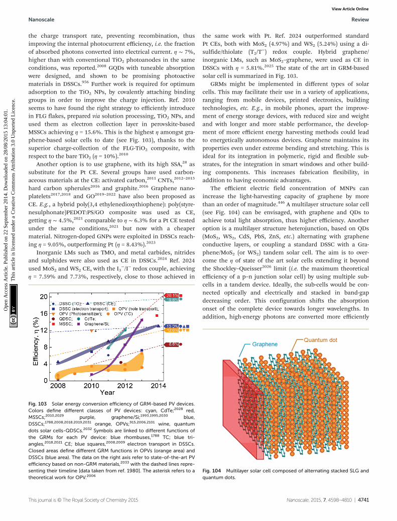
the charge transport rate, preventing recombination, thusimproving the internal photocurrent efficiency, i.e. the fractionof absorbed photons converted into electrical current. η ∼ 7%,higher than with conventional TiO2 photoanodes in the sameconditions, was reported.2008 GQDs with tuneable absorptionwere designed, and shown to be promising photoactivematerials in DSSCs.956 Further work is required for optimumadsorption to the TiO2 NPs, by covalently attaching bindinggroups in order to improve the charge injection. Ref. 2010seems to have found the right strategy to efficiently introducein FLG flakes, prepared via solution processing, TiO2 NPs, andused them as electron collection layer in perovskite-basedMSSCs achieving η = 15.6%. This is the highest η amongst gra-phene-based solar cells to date (see Fig. 103), thanks to thesuperior charge-collection of the FLG-TiO2 composite, withrespect to the bare TiO2 (η = 10%).2010
Another option is to use graphene, with its high SSA,28 assubstitute for the Pt CE. Several groups have used carbon-aceous materials at the CE: activated carbon,2011 CNTs,2012–2015
hard carbon spherules2016 and graphite.2016 Graphene nano-platelets2017,2018 and GO2019–2022 have also been proposed asCE. E.g., a hybrid poly(3,4 ethylenedioxythiophene): poly(styre-nesulphonate)PEDOT:PS/GO composite was used as CE,getting η ∼ 4.5%,2021 comparable to η ∼ 6.3% for a Pt CE testedunder the same conditions,2021 but now with a cheapermaterial. Nitrogen-doped GNPs were exploited in DSSCs reach-ing η = 9.05%, outperforming Pt (η = 8.43%).2023
Inorganic LMs such as TMO, and metal carbides, nitridesand sulphides were also used as CE in DSSCs.2024 Ref. 2024used MoS2 and WS2 CE, with the I3
−/I− redox couple, achievingη = 7.59% and 7.73%, respectively, close to those achieved in
the same work with Pt. Ref. 2024 outperformed standardPt CEs, both with MoS2 (4.97%) and WS2 (5.24%) using a di-sulfide/thiolate (T2/T
−) redox couple. Hybrid graphene/inorganic LMs, such as MoS2–graphene, were used as CE inDSSCs with η = 5.81%.2025 The state of the art in GRM-basedsolar cell is summarized in Fig. 103.
GRMs might be implemented in different types of solarcells. This may facilitate their use in a variety of applications,ranging from mobile devices, printed electronics, buildingtechnologies, etc. E.g., in mobile phones, apart the improve-ment of energy storage devices, with reduced size and weightand with longer and more stable performance, the develop-ment of more efficient energy harvesting methods could leadto energetically autonomous devices. Graphene maintains itsproperties even under extreme bending and stretching. This isideal for its integration in polymeric, rigid and flexible sub-strates, for the integration in smart windows and other build-ing components. This increases fabrication flexibility, inaddition to having economic advantages.
The efficient electric field concentration of MNPs canincrease the light-harvesting capacity of graphene by morethan an order of magnitude.446 A multilayer structure solar cell(see Fig. 104) can be envisaged, with graphene and QDs toachieve total light absorption, thus higher efficiency. Anotheroption is a multilayer structure heterojunction, based on QDs(MoS2, WS2, CdS, PbS, ZnS, etc.) alternating with grapheneconductive layers, or coupling a standard DSSC with a Gra-phene/MoS2 (or WS2) tandem solar cell. The aim is to over-come the η of state of the art solar cells extending it beyondthe Shockley–Queisser2026 limit (i.e. the maximum theoreticalefficiency of a p–n junction solar cell) by using multiple sub-cells in a tandem device. Ideally, the sub-cells would be con-nected optically and electrically and stacked in band-gapdecreasing order. This configuration shifts the absorptiononset of the complete device towards longer wavelengths. Inaddition, high-energy photons are converted more efficiently
Fig. 103 Solar energy conversion efficiency of GRM-based PV devices.Colors define different classes of PV devices: cyan, CdTe;2028 red,MSSCs;2010,2029 purple, graphene/Si;1993,1995,2030 blue,DSSCs;1788,2008,2018,2019,2031 orange, OPVs;915,2006,2101 wine, quantumdots solar cells-QDSCs.2032 Symbols are linked to different functions ofthe GRMs for each PV device: blue rhombuses,1788 TC; blue tri-angles,2018,2021 CE; blue squares,2008,2009 electron transport in DSSCs.Closed areas define different GRM functions in OPVs (orange area) andDSSCs (blue area). The data on the right axis refer to state-of-the-art PVefficiency based on non-GRM materials,2033 with the dashed lines repre-senting their timeline [data taken from ref. 1980]. The asterisk refers to atheoretical work for OPV.2006
Fig. 104 Multilayer solar cell composed of alternating stacked SLG andquantum dots.
Nanoscale Review
This journal is © The Royal Society of Chemistry 2015 Nanoscale, 2015, 7, 4598–4810 | 4741
Ope
n A
cces
s A
rtic
le. P
ublis
hed
on 2
2 Se
ptem
ber
2014
. Dow
nloa
ded
on 2
8/08
/201
5 13
:04:
01.
Thi
s ar
ticle
is li
cens
ed u
nder
a C
reat
ive
Com
mon
s A
ttrib
utio
n 3.
0 U
npor
ted
Lic
ence
.View Article Online

since thermalisation losses of the generated e–h pairs arereduced with the graded band gap structure. E.g. in a series-connected double-junction device, the ideal optical band gapsare ∼1.6–1.7 eV for the top cell and ∼1.0–1.1 eV for the bottomcell, which extends the efficiency limit to ∼45%.2027
Another possibility is to assemble hybrid graphene/nano-diamonds,2034,2035 motivated by the properties of bothmaterials, and possible interactions between sp2 and sp3
carbon.2036 The <111> diamond surface could form an idealinterface for heteroepitaxial graphene, with ∼2% mismatch.The armchair diamond rings on the <111> surface can beinterfaced to the 6-membered C rings of graphene. There areseveral impacting interests in these interfaces. Un-doped nano-diamond could serve as gate insulator. A controllablefunctionalization of nanodiamond may be used to tune gra-phene’s μ and work function other than the optical properties.This might be achieved by coupling graphene, using organicchemistry routes via linkers with functional properties, tonanodiamond. In these solar cells, conductive B-doped nano-diamond would serve as anode, while graphene would be thecathode. If donor–acceptor organic dyes are used for suchinterfacing, the proposed full carbon structure would haveeffective charge transfer from the HOMO of the organic dye tothe diamond valence band, and in a reversed process on thegraphene/LUMO side.
Another approach relies in the use of chemically syn-thesized GNRs and/or GQDs sensitizers in solar cells. GQDshave been synthesized with molar extinction coefficients (∼1 ×10⁵ M−1 cm−1,956 ∼one order of magnitude larger than in-organic dyes (e.g. ruthenium complexes),956 commonly used inDSSCs) and absorption edge beyond 900 nm.956
10.5. Thermoelectric devices
Thermoelectric (TE) devices, i.e. solid-state devices (Fig. 105)that generate electricity from a T gradient,2037 are ideal torecover waste thermal energy.2037 Inorganic layered com-pounds are promising as thermoelectric materials, to extractelectrical energy from a T gradient (e.g. waste heat).2037 Suchmaterials need high Seebeck coefficient (S), high σ and lowκ.2037,2038 These properties are found in some LMs such asBi2Te3.
111 The effectiveness of a TE device is assessed in twoways: by its Carnot efficiency (i.e. the maximum efficiencypossible for converting a given amount of thermal energy intowork) and by a material-dependent factor called the TE figureof merit zT (105); zT = TS2σ/k,2038 where S is the Seebeck coeffi-cient, T the temperature, κ the thermal conductivity and z =S2σ/k.2037,2038 Thus, TE materials require high S and σ values,and low κ.2039 In order to optimize zT, phonons must experi-ence a high scattering rate, thus lowering κ2039 (i.e. as in aglass) while electrons must have little scattering, maintaininghigh σ (i.e. as in a crystal).2040 It was shown that κ of Bi2Te3 canbe suppressed by reducing the grain size.2041 The ideal way todo this would be LPE.38 Thus LPE-Bi2Te3 devices could bemade with figure of merit zT > 1.
Many LMs have high S and low κ.111 The low σ generallymeans they are unsuited to thermoelectric applications.
However, since LMs can be exfoliated in liquids, it could bepossible to blend them with nanoconductors, such as CNTs orgraphene. This may increase σ, while retaining S.2037 The chal-lenge will be to keep κ at low values. To achieve this it is key tounderstand the physics of thermal transport in nanostructureddisordered networks.
Graphene has high σ74 but also high κ,2042 a combinationthat it is not ideal for TE devices. However, it is possible totailor the thermal transport properties of graphene by nano-structuring techniques, such as defects2043 and isotope2044
engineering, edge roughness2043 or introducing periodic nano-holes.2045 The combination of geometrical structuring, GNRswith predefined geometries,320 and isotopically modified gra-phene with 13C2044 can reduce κ by up to two orders of magni-tude with respect to pristine graphene.2046 Ref. 2046 estimatedthat zT up to 3.25 can be achieved exploiting GNRs having achevron-like geometry.2046
10.6. Nanogenerators
Self-powering devices are a new paradigm in nanotechnologyand green energy for sustainable self-sufficient micro/nano-systems, of critical importance for sensing, medicine, infra-structure/environmental monitoring, defense technology andpersonal electronics.2047
The combination of mono-atomic thickness with high rigid-ity (Young modulus 1 TPa) and maximal strength (130 GPa),18
as well as unique optoelectronic995 characteristics, makes gra-phene a candidate for NOEMS (nano-optoelectromechanicalsystems) energy harvesting nanodevices (nanogenerators –
NGs), which efficiently convert the energy from environmentalsources, such as ambient noise or electromagnetic radiations(from RF to visible wavelength), to mechanical vibrations. Thiswould enable mechanical compliances and resonant frequen-cies matching the energy levels and characteristic frequenciesof non-explored energy sources arising at the nanoscale. When
Fig. 105 Schematic illustration of power generation in a TE devicebased on Bi2Te3 LMs or GNRs. A T gradient, ΔT, causes charge carriers inthe material to diffuse, resulting in current flow through the externalcircuit. Adapted from ref. 1841.
Review Nanoscale
4742 | Nanoscale, 2015, 7, 4598–4810 This journal is © The Royal Society of Chemistry 2015
Ope
n A
cces
s A
rtic
le. P
ublis
hed
on 2
2 Se
ptem
ber
2014
. Dow
nloa
ded
on 2
8/08
/201
5 13
:04:
01.
Thi
s ar
ticle
is li
cens
ed u
nder
a C
reat
ive
Com
mon
s A
ttrib
utio
n 3.
0 U
npor
ted
Lic
ence
.View Article Online

the energy source is noisy, non-linear MEMS with a broadbandor a low frequency spectrum can be convenient as energy har-vesters, based on the mechanical non-linearities of suspendedGNRs.
Particularly interesting is the merging of energy harvestingand optoelectronic concepts and technologies, when envisa-ging the enhancement of light to nanomechanical vibrationsconversion on a NOEMS device by using the higher opticalabsorption of doped or nanopatterned1578 graphenenanostructures.
Other NGs2048 exploiting piezoelectric,2049,2050 triboelec-tric2051,2052 and pyroelectric2053 effects have been investigatedas efficient energy harvesting systems from the living environ-ment.2047 A complete, flexible, and integrated system capable
of harvesting and storing energy from the natural contractileand relaxation motions of internal organs such as heart, lung,and diaphragm was recently demonstrated with efficiency of∼2%.2054
Nanogenerators integrated with graphene films were shownto possess outstanding mechanical and optical properties,thus offering unique benefits in high-performance flexible andtransparent devices.2055 Ref. 2055 demonstrated how all devicecomponents, including piezoelectric (PZT) materials and gra-phene electrodes, can be printed onto a plastic substrate,using a low T transfer process.
The resulting graphene-based PZT exhibited good mechan-ical bendability, Tr and simple device design, compatible withconventional batch fabrication steps.2055 The output power of
Fig. 106 Energy applications timeline. The white rectangles summarize the main targets to be achieved in a timeframe of 10 years.
Nanoscale Review
This journal is © The Royal Society of Chemistry 2015 Nanoscale, 2015, 7, 4598–4810 | 4743
Ope
n A
cces
s A
rtic
le. P
ublis
hed
on 2
2 Se
ptem
ber
2014
. Dow
nloa
ded
on 2
8/08
/201
5 13
:04:
01.
Thi
s ar
ticle
is li
cens
ed u
nder
a C
reat
ive
Com
mon
s A
ttrib
utio
n 3.
0 U
npor
ted
Lic
ence
.View Article Online

the graphene-based PZT efficiently powered commerciallyavailable electronic components (e.g. LCDs and LEDs) in aself-powered mode, without any external electrical supply.2055
These results are encouraging in view of further developmentof graphene-based harvesting systems, particularly for appli-cations that require flexibility and semi-transparency.
The timeline for the energy applications is shown inFig. 106. The main targets are: 3 years: Pristine and functiona-lized GRMs for composites and intercalated compounds; Pro-cessing of GRMs for PV wet technology. 3–7 years: Highcapacitance GRM-based mesoporous electrodes; PV electrodesand absorbers. 7–10 years: flexible PV cells; Light electricaland hydrogen storage systems.
11. Composites
The properties of graphene can be exploited for applicationswhere, rather than a monolayer on a substrate, large quantitiesare processed from solution or melt to be included in bulkmaterials, like polymers.2056 These applications require lowcost, high-processability in solvents and polymers and tune-able chemical properties.
An advantage of graphene over other nanomaterials is thatit can be produced either by bottom-up assembly of smalleratoms and molecules or top-down exfoliation of graphitestacks. Unlike CNTs, graphene can be produced on tonscale2057 without high T and metal catalysts, allowing cheapproduction for different large scale applications.2058
Graphene–based solutions may be used for antistatic, EMIshielding, conductive inks, and gas barrier applications. Inprinciple, the production technology is simple and developedwith most of the graphite mining companies having programson LPE graphene.2059 Major developments should be made inthe area of chemical derivatives of graphene in order tocontrol electrical conductivity and optical properties of thefinal products.
Graphene, being an inert (unreactive under ambient con-ditions) material,2060 can also act as a corrosionbarrier.2061–2064 Since it can be grown on the surface of mostmetals under the right conditions, it could form a protectiveconformal layer, i.e. it could be used on rather complex surfaces.However, it might be difficult to precisely control the chemicalproperties and uniformity of graphene growth on arbitrary sub-strates. Also, the T involved in such direct growth approachesmay alter the properties of the underlying metal substrate.
While the addition of CNTs to polymer matrices was shownto improve mechanical, electrical and thermal properties2065 atlow loadings, the challenge is now to exfoliate graphite to SLGin sufficiently large quantity to be used as an inexpensive andfeasible substitute to CNTs and traditional filler materials.Incorporation of well-dispersed graphene-sheets into polymersat low filler content (from 0.1% to 3% w/v [weight/volume])improves the mechanical properties, e.g. Young modulus, ofthe polymer,2066 see Fig. 107 for a comparison of Youngmodulus as function of density of graphene with respect toother materials.
Fig. 107 Chart of Young’s modulus as a function of density comparing graphene properties to more traditional materials. Green ellipse, foams;cyan ellipse, elastomers; blue ellipse, polymers; olive triangle, natural materials; purple ellipse, composites; magenta triangle, metals; orange ellipse,ceramics. The white circles and ellipses are referring to a particular material inside each of the listed classes of materials. Note the axes are in logar-ithmic scale. Graphene density was taken as 2200 kg m−3.2085 PVC, Polyvinyl chloride, PTFE, Polytetrafluoroethylene; GFRC, glass fiber reinforcedconcrete; CFRC, ceramic fiber reinforced concrete.
Review Nanoscale
4744 | Nanoscale, 2015, 7, 4598–4810 This journal is © The Royal Society of Chemistry 2015
Ope
n A
cces
s A
rtic
le. P
ublis
hed
on 2
2 Se
ptem
ber
2014
. Dow
nloa
ded
on 2
8/08
/201
5 13
:04:
01.
Thi
s ar
ticle
is li
cens
ed u
nder
a C
reat
ive
Com
mon
s A
ttrib
utio
n 3.
0 U
npor
ted
Lic
ence
.View Article Online
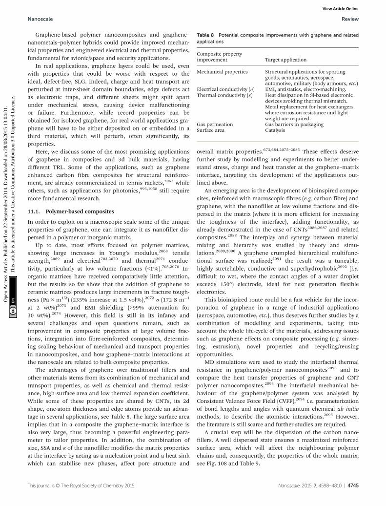
Graphene-based polymer nanocomposites and graphene–nanometals–polymer hybrids could provide improved mechan-ical properties and engineered electrical and thermal properties,fundamental for avionic/space and security applications.
In real applications, graphene layers could be used, evenwith properties that could be worse with respect to theideal, defect-free, SLG. Indeed, charge and heat transport areperturbed at inter-sheet domain boundaries, edge defects actas electronic traps, and different sheets might split apartunder mechanical stress, causing device malfunctioningor failure. Furthermore, while record properties can beobtained for isolated graphene, for real world applications gra-phene will have to be either deposited on or embedded in athird material, which will perturb, often significantly, itsproperties.
Here, we discuss some of the most promising applicationsof graphene in composites and 3d bulk materials, havingdifferent TRL. Some of the applications, such as grapheneenhanced carbon fibre composites for structural reinforce-ment, are already commercialized in tennis rackets,2067 whileothers, such as applications for photonics,995,1058 still requiremore fundamental research.
11.1. Polymer-based composites
In order to exploit on a macroscopic scale some of the uniqueproperties of graphene, one can integrate it as nanofiller dis-persed in a polymer or inorganic matrix.
Up to date, most efforts focused on polymer matrices,showing large increases in Young’s modulus,2068 tensilestrength,2069 and electrical703,2070 and thermal2071 conduc-tivity, particularly at low volume fractions (<1%).703,2070 In-organic matrices have received comparatively little attention,but the results so far show that the addition of graphene toceramic matrices produces large increments in fracture tough-ness (Pa × m1/2) (235% increase at 1.5 vol%),2072 σ (172 S m−1
at 2 wt%)2073 and EMI shielding (>99% attenuation for30 wt%).2074 However, this field is still in its infancy andseveral challenges and open questions remain, such asimprovement in composite properties at large volume frac-tions, integration into fibre-reinforced composites, determin-ing scaling behaviour of mechanical and transport propertiesin nanocomposites, and how graphene–matrix interactions atthe nanoscale are related to bulk composite properties.
The advantages of graphene over traditional fillers andother materials stems from its combination of mechanical andtransport properties, as well as chemical and thermal resist-ance, high surface area and low thermal expansion coefficient.While some of these properties are shared by CNTs, its 2dshape, one-atom thickness and edge atoms provide an advan-tage in several applications, see Table 8. The large surface areaimplies that in a composite the graphene–matrix interface isalso very large, thus becoming a powerful engineering para-meter to tailor properties. In addition, the combination ofsize, SSA and κ of the nanofiller modifies the matrix propertiesat the interface by acting as a nucleation point and a heat sinkwhich can stabilise new phases, affect pore structure and
overall matrix properties.673,684,2075–2085 These effects deservefurther study by modelling and experiments to better under-stand stress, charge and heat transfer at the graphene–matrixinterface, targeting the development of the applications out-lined above.
An emerging area is the development of bioinspired compo-sites, reinforced with macroscopic fibres (e.g. carbon fibre) andgraphene, with the nanofiller at low volume fractions and dis-persed in the matrix (where it is more efficient for increasingthe toughness of the interface), adding functionality, asalready demonstrated in the case of CNTs2086,2087 and relatedcomposites.2088 The interplay and synergy between materialmixing and hierarchy was studied by theory and simu-lations.2089,2090 A graphene crumpled hierarchical multifunc-tional surface was realized;2091 the result was a tuneable,highly stretchable, conductive and superhydrophobic2092 (i.e.difficult to wet, where the contact angles of a water dropletexceeds 150°) electrode, ideal for next generation flexibleelectronics.
This bioinspired route could be a fast vehicle for the incor-poration of graphene in a range of industrial applications(aerospace, automotive, etc.), thus deserves further studies by acombination of modelling and experiments, taking intoaccount the whole life-cycle of the materials, addressing issuessuch as graphene effects on composite processing (e.g. sinter-ing, extrusion), novel properties and recycling/reusingopportunities.
MD simulations were used to study the interfacial thermalresistance in graphene/polymer nanocomposites2093 and tocompare the heat transfer properties of graphene and CNTpolymer nanocomposites.2093 The interfacial mechanical be-haviour of the graphene/polymer system was analysed byConsistent Valence Force Field (CVFF),2094 i.e. parameterizationof bond lengths and angles with quantum chemical ab initiomethods, to describe the atomistic interactions.2095 However,the literature is still scarce and further studies are required.
A crucial step will be the dispersion of the carbon nano-fillers. A well dispersed state ensures a maximized reinforcedsurface area, which will affect the neighbouring polymerchains and, consequently, the properties of the whole matrix,see Fig. 108 and Table 9.
Table 8 Potential composite improvements with graphene and relatedapplications
Composite propertyimprovement Target application
Mechanical properties Structural applications for sportinggoods, aeronautics, aerospace,automotive, military (body armours, etc.)
Electrical conductivity (σ) EMI, antistatics, electro-machining.Thermal conductivity (κ) Heat dissipation in Si-based electronic
devices avoiding thermal mismatch.Metal replacement for heat exchangerswhere corrosion resistance and lightweight are required.
Gas permeation Gas barriers in packagingSurface area Catalysis
Nanoscale Review
This journal is © The Royal Society of Chemistry 2015 Nanoscale, 2015, 7, 4598–4810 | 4745
Ope
n A
cces
s A
rtic
le. P
ublis
hed
on 2
2 Se
ptem
ber
2014
. Dow
nloa
ded
on 2
8/08
/201
5 13
:04:
01.
Thi
s ar
ticle
is li
cens
ed u
nder
a C
reat
ive
Com
mon
s A
ttrib
utio
n 3.
0 U
npor
ted
Lic
ence
.View Article Online

Therefore, large efforts were devoted2096 to achievinghomogeneous and well-dispersed systems by developingeither covalent or non-covalent functionalisation of the fillersurface.
The initial aim is to increase the composite modulus andstrength by factors 2–4 with respect to plastic, at low loadinglevel, <1%, so that the filler provides reinforcement withoutdegrading any other properties nor significantly increasingweight. Later, one might expect to produce higher volume frac-tions, higher performance composites, with mechanical pro-perties exceeding those of structural materials, such as steel,at a fraction of the density. In addition, adding GRMs to plas-tics may reduce gas permeability. This is very important forthe beverage industry. E.g., beer manufacturers want to movefrom glass bottles to PET. However the shelf life of beer in PETis ∼2 weeks (cf. 30 weeks in glass).198,199,2115 To increase thisshelf life, both oxygen and CO2 permeability, need to be cut bya factor of ∼5.199 DLC has been successfully used for suchapplications.198,199,2116 The permeability of a given plasticcould be reduced by more than a factor of 10 for <5 vol%loading of platelets with aspect ratio >1000.2117 Thus, gra-phene could allow one to reduce the mass of plastic per bottle,i.e. reduce wall thickness.
Epoxy resin is a thermosetting polymer (i.e. it cross-links andtoughens with T) and is widely used in various industries,including coatings, adhesives, electrical insulators, and compo-
sites.2118 Epoxy has excellent mechanical and chemical pro-perties, including good dielectric properties,2119 highdimensional stability (the ability of a material to hold its shapeover a period of time and for varying amounts of applied temp-erature, moisture, pressure, or other stress),2120 hardness,2121
flexibility,2122 and excellent chemical resistance (the ability of amaterial to avoid the permeability of different ions or mole-cules).2123 However, epoxy burns easily,2124 so research hasbeen carried out to obtain a fire retardant epoxy.2125,2126 One ofthe most efficient ways to reduce the heat release rate, slowingthermal degradation of the polymer matrix and inhibiting heatand flammable gas release, is to use carbon materials.2127 Gra-phene sheets hold potential as new nanofiller and may be pre-ferred over other nanofillers (CNT, carbon nanofiber, graphitenanoplatelets, etc.) owing to its higher surface area, aspect ratio,tensile strength, κ and σ.2128
Blended GO with epoxy, with high κ2071 (1.91 W mK−1) withrespect to thermally conductive epoxy (∼1 W mK−1), has beendemonstrated.2076 Nanocomposites with 5 wt% GO haveshown a 4-fold increment of κ compared to pristine epoxy.2076
A comparison of the mechanical reinforcement of grapheneflakes, SWNTs and MWNTs on the epoxy matrix at a nanofillercontent of 0.1 wt% was reported in ref. 2129 indicating thatgraphene flakes out-perform CNTs in terms of Young’smodulus, tensile strength and fracture toughness of the result-ing composite.
Table 9 Summary of mechanical properties of graphene/polymer nanocomposites
Polymer ReinforcementsGrapheneconcentration (vol%)
Modulusincrease (%)
Tensile strengthincrease (%)
Ultimate strainincrease (%) Ref.
PVA GO 2.5 128 70 32 2097PVA GO 0.49 62 76 −70 2098PMMA GO 1.7 54 N/A N/A 2099PCL GO 2.4 108 36 −90 2100PCL GO 0.46 50 N/A N/A 2101Epoxy FG 0.05) 31 40 N/A 2129PEN FG 2.4 57 N/A N/A 2102PCA FG 1.3 25 N/A N/A 2103PMMA FG (0.005, 0.5) 33, 80 N/A N/A 36PVDF FG 3.1 92 N/A N/A 2104SAN FG 2.3 34 N/A −58 2105Natural rubber FG 1.2 750 N/A N/A 2106PDMS FG 2.2 1100 N/A N/A 2106Styrene-butadienerubber
FG 0.8 390 N/A N/A 2106
TPU FG 1.5 43 −23 −15 2107Silicone foam FG 0.12 200 N/A N/A 2108PVA Acid functionalized graphene 0.34 35 N/A N/A 2109PMMA Amine treated acid
functionalized graphene0.3 70 N/A N/A 2109
TPU FG 1.6 250 N/A N/A 21101.6 680 N/A N/A1.5 210 N/A N/A
GO 1.6 490–900 N/A N/A 2110PS PS-functionalized chemically
reduced GO0.4 57 N/A N/A 2111
TPU chemically reducedsulfonated-graphene
0.5 120 75 N/A 2112
TPU GO 2.4 900 −19 −60 2113PAN Exfoliation alkali GIC 2.1 100 N/A N/A 2114
Review Nanoscale
4746 | Nanoscale, 2015, 7, 4598–4810 This journal is © The Royal Society of Chemistry 2015
Ope
n A
cces
s A
rtic
le. P
ublis
hed
on 2
2 Se
ptem
ber
2014
. Dow
nloa
ded
on 2
8/08
/201
5 13
:04:
01.
Thi
s ar
ticle
is li
cens
ed u
nder
a C
reat
ive
Com
mon
s A
ttrib
utio
n 3.
0 U
npor
ted
Lic
ence
.View Article Online
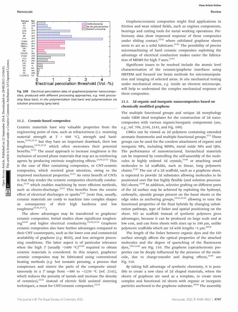
11.2. Ceramic-based composites
Ceramic materials have very valuable properties from theengineering point of view, such as refractoriness (i.e. retainingmaterial strength at T > 600 °C), strength and hard-ness,2130,2131 but they have an important drawback, their lowtoughness,2130,2131 which often overcomes their potentialbenefits.2132 The usual approach to increase toughness is theinclusion of second phase materials that may act as reinforcingagents by producing extrinsic toughening effects.2130,2131 Thisis the case of fiber containing composites, or CNT-ceramiccomposites, which received great attention, owing to theimproved mechanical properties.2133 An extra benefit of CNTsis that they render the ceramic composites electrically conduc-tive,2134 which enables machining by more efficient methods,such as electro-discharge.2135 This benefits from the erosiveeffect of electrical discharges or sparks2135 (note that, usually,ceramic materials are costly to machine into complex shapesas consequence of their high hardness and lowtoughness2136,2137).
The above advantages may be transferred to graphene/ceramic composites. Initial studies show significant toughen-ing2129 and higher electrical conductivity.2138,2139 Grapheneceramic composites also have further advantages compared totheir CNT counterparts, such as the lower cost and commercialavailability of graphene (e.g. RGO), and less stringent proces-sing conditions. The latter aspect is of particular relevancewhen the high T (usually >1400 °C)2140 required to obtainceramic materials is considered. In this respect, graphene/ceramic composites may be fabricated using conventionalheating methods (e.g. hot isostatic pressing, a process thatcompresses and sinters the parts of the composite simul-taneously in a T range from ∼480 to ∼1230 °C (ref. 2141),which reduces the porosity of metals and increase the densityof ceramics),2141 instead of electric field assisted sinteringtechniques, a must for CNT/ceramic composites.2134
Graphene/ceramic composites might find applications infriction and wear related fields, such as engines components,bearings and cutting tools for metal working operations. Pre-liminary data show improved response of these compositesunder sliding contact,2142 where exfoliated graphene sheetsseem to act as a solid lubricant.2142 The possibility of precisemicromachining of hard ceramic composites exploiting theadvantage of electrical conduction makes easier the fabrica-tion of MEMS for high T uses.2143
Significant issues to be resolved include the atomic levelcharacterization of the ceramic/graphene interfaces usingHRTEM and focused ion beam methods for micromanipula-tion and imaging of selected areas. In situ mechanical testingunder mechanical stress, e.g. inside an electron microscope,will help to understand the complex mechanical response ofthese composites.
11.3. 2d organic and inorganic nanocomposites based onchemically modified graphene
The multiple functional groups and unique 2d morphologymake GRM ideal templates for the construction of 2d nano-composites with various organic/inorganic components (see,e.g., ref. 709, 2144, 2145, and Fig. 109).
CMGs can be viewed as 2d polymers containing extendedaromatic frameworks and multiple functional groups.673 Thesegroups can be used for the covalent attachment of organic andinorganic NPs, including MNPs, metal oxide NPs and QDs.The performance of nanostructured, hierarchical materialscan be improved by controlling the self-assembly of the mole-cules in highly ordered 3d crystals,2146 or attaching smallmolecules to 1d scaffolds, such as linear, long polymericchains.2147 The use of a 2d scaffold, such as a graphene sheet,is expected to provide 2d substrates allowing molecules to bepositioned over flat but highly flexible (and solution processa-ble) sheets.2148 In addition, selective grafting on different partsof the 2d surface may be achieved by exploiting the hydroxyl,carboxylic, epoxide groups present on the basal sheets or theedge sides as anchoring groups,2145,2145 allowing to tune thefunctional properties of the final hybrids by changing substi-tution pathways, type of linker and spatial positioning on thesheet. GO as scaffold instead of synthetic polymers givesadvantages, because it can be produced on large scale and atlow cost, and can form sheets with sizes up to 100 μm, unlikepolymeric scaffolds which are 1d with lengths <1 μm.2058
The length of the linker between organic dyes and the GOsurface strongly affects the optical properties of the attachedmolecules and the degree of quenching of the fluorescentdyes,709,2148 see Fig. 110. The graphene (opto)electronic pro-perties can be deeply influenced by the presence of the mole-cule, due to charge-transfer and doping effects,2149 seeFig. 110.
By taking full advantage of synthetic chemistry, it is poss-ible to create a new class of 2d shaped materials, where thesheets of graphene are used as a template, to create morecomplex and functional 2d sheets with organic or inorganicparticles anchored to the graphene substrate.2058 The assembly
Fig. 108 Electrical percolation data of graphene/polymer nanocompo-sites, produced with different processing approaches, e.g. melt proces-sing (blue bars), in situ polymerization (red bars) and polymerization viasolution processing (grey bars).
Nanoscale Review
This journal is © The Royal Society of Chemistry 2015 Nanoscale, 2015, 7, 4598–4810 | 4747
Ope
n A
cces
s A
rtic
le. P
ublis
hed
on 2
2 Se
ptem
ber
2014
. Dow
nloa
ded
on 2
8/08
/201
5 13
:04:
01.
Thi
s ar
ticle
is li
cens
ed u
nder
a C
reat
ive
Com
mon
s A
ttrib
utio
n 3.
0 U
npor
ted
Lic
ence
.View Article Online
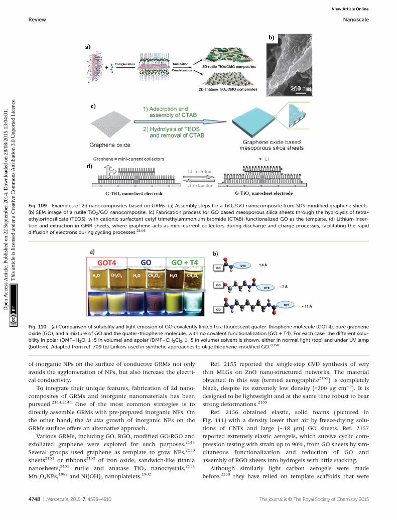
of inorganic NPs on the surface of conductive GRMs not onlyavoids the agglomeration of NPs, but also increase the electri-cal conductivity.
To integrate their unique features, fabrication of 2d nano-composites of GRMs and inorganic nanomaterials has beenpursued.2144,2145 One of the most common strategies is todirectly assemble GRMs with pre-prepared inorganic NPs. Onthe other hand, the in situ growth of inorganic NPs on theGRMs surface offers an alternative approach.
Various GRMs, including GO, RGO, modified GO/RGO andexfoliated graphene were explored for such purposes.2144
Several groups used graphene as template to grow NPs,2150
sheets2151 or ribbons2152 of iron oxide, sandwich-like titaniananosheets,2153 rutile and anatase TiO2 nanocrystals,2154
Mn3O4NPs,1882 and Ni(OH)2 nanoplatelets.
1902
Ref. 2155 reported the single-step CVD synthesis of verythin MLGs on ZnO nano-structured networks. The materialobtained in this way (termed aerographite2155) is completelyblack, despite its extremely low density (<200 μg cm−3). It isdesigned to be lightweight and at the same time robust to bearstrong deformations.2155
Ref. 2156 obtained elastic, solid foams (pictured inFig. 111) with a density lower than air by freeze-drying solu-tions of CNTs and large (∼18 μm) GO sheets. Ref. 2157reported extremely elastic aerogels, which survive cyclic com-pression testing with strain up to 90%, from GO sheets by sim-ultaneous functionalization and reduction of GO andassembly of RGO sheets into hydrogels with little stacking.
Although similarly light carbon aerogels were madebefore,2158 they have relied on template scaffolds that were
Fig. 109 Examples of 2d nanocomposites based on GRMs. (a) Assembly steps for a TiO2/GO nanocomposite from SDS-modified graphene sheets.(b) SEM image of a rutile TiO2/GO nanocomposite. (c) Fabrication process for GO based mesoporous silica sheets through the hydrolysis of tetra-ethylorthosilicate (TEOS), with cationic surfactant cetyl trimethylammonium bromide (CTAB)-functionalized GO as the template. (d) Lithium inser-tion and extraction in GMR sheets, where graphene acts as mini-current collectors during discharge and charge processes, facilitating the rapiddiffusion of electrons during cycling processes.2144
Fig. 110 (a) Comparison of solubility and light emission of GO covalently linked to a fluorescent quater-thiophene molecule (GOT4), pure grapheneoxide (GO), and a mixture of GO and the quater-thiophene molecule, with no covalent functionalization (GO + T4). For each case, the different solu-bility in polar (DMF–H2O, 1 : 5 in volume) and apolar (DMF–CH2Cl2, 1 : 5 in volume) solvent is shown, either in normal light (top) and under UV lamp(bottom). Adapted from ref. 709 (b) Linkers used in synthetic approaches to oligothiophene-modified GO.2058
Review Nanoscale
4748 | Nanoscale, 2015, 7, 4598–4810 This journal is © The Royal Society of Chemistry 2015
Ope
n A
cces
s A
rtic
le. P
ublis
hed
on 2
2 Se
ptem
ber
2014
. Dow
nloa
ded
on 2
8/08
/201
5 13
:04:
01.
Thi
s ar
ticle
is li
cens
ed u
nder
a C
reat
ive
Com
mon
s A
ttrib
utio
n 3.
0 U
npor
ted
Lic
ence
.View Article Online

later etched away, a technique that limits the size of the finalstructure.2157 The resulting aerogels show density as low as3 mg cm−3, yet the structure can fully recover without fractureeven after 90% compression, suggesting applications in shockdamping.2159
11.4. Photonic polymer composites
The demand in optical networking for photonic componentsthat meet performance criteria as well as economic require-ments opens the door to novel technologies capable of high-yield, low-cost manufacturing, while delivering high perform-ance and enabling unique functions.2160 An optical communi-cation system requires light sources and detectors, but manyadditional components make up modern transmission net-works. Until the end of the 1980s, these components, includ-ing beam splitters, multiplexers and switches, consisted ofbulk optics elements, such as lenses and prisms. Bulk opticalcomponents, however, are inconvenient to handle, highlysensitive to misalignment and prone to instability. All ofthese problems are avoided in integrated optics systems.2161
These combine miniaturised optical components and wave-guides in a highly condensed chip-based device. Theircompact, planar layout has clear advantages over bulk opticswhen deployed in complex systems. Integration permits thereduction of complex multi-function photonic circuits on aplanar substrate.
Polymeric materials are the ideal choice for such an inte-gration platform.2160,2162,2163 They are easily manipulated bymethods such as embossing, stamping, sawing, wet or dryetching. They have a low-cost, RT fabrication process. Polymerscan be synthesized with customer defined optical character-istics, such as selective transparency bands in different spec-tral ranges, variable refractive indexes, low birefringence, otherthan high laser damage threshold and thermal stability. More-over, the polymers must be easily processable during devicefabrication and be economic.2164 Polymers traditionally usedfor optical applications include PMMA,2160 polycarbonate2165
and epoxy resins.2160
Deuterated2164 or halogenated polyacrylates2164 and fluori-nated polyimides2160 were developed to address specificissues, such as optical losses,2166 heat2164 and environmentalstability.2164 Water-soluble polymers, such as
PVA,1353,2165,2167–2169 and cellulose derivatives, such as sodiumcarboxymethyl cellulose,1353,2170 have been widely used bothfor CNT and graphene-based SAs,1353,2171–2173 since stable,high-concentration dispersions can be readily prepared.1353
From the fabrication perspective, PVA is more attractive,because of its mechanical properties.1353 To prepare environ-mentally stable polymer composites, in particular, againsthumidity and T, graphene can be directly exfoliated in organicsolvents.35 The dispersions are suitable for moisture resistantpolymers, such as Polycarbonate and PMMA, or copolymers,such as SMMA.1353 Siloxane polymers have many attractiveattributes, such as stable optical performance with low loss,making them viable for polymer waveguides. These can bespin-coated from uncured precursors or polymer solutions andthen patterned into the specific waveguide geometries usingeither reactive ion etch or direct exposure to UV light patterns.
Precise control of the refractive index of both core and clad-ding material can optimise light transmission. Like inorganicmaterials,2174 polymers can be doped to take advantage ofoptical properties associated with the dopant.
Optical amplifiers are an important component in opticalcommunications.2175 They are needed to enhance signals, par-ticularly in order to compensate for the intrinsic losses due tofibre propagation and splitting, switching and multiplexingoperations. Amplifiers can be housed in optical fibres or inintegrated optics components. EDFAs2174 consist of an activeregion formed from a length of Er-doped silica fibre. They areoften used in telecommunication networks to amplify opticalsignals in the 1310 and 1550 nm windows. With the emer-gence of polymer optical fibres,2176 the natural progressionfrom silica-based EDFAs is the doping of rare earths into poly-mers.2177 There has also been increasing interest in dopingrare earths in inorganic and organic waveguide components tomake waveguide optical amplifiers.2178 The ease of integratedcircuit fabrication provided by polymers, coupled with theexpected high-gain performance in rare-earth polymermaterials, lead to increased activity in this field.2179,2180
Many of the advantages of polymer materials discussed forcommunications systems also apply to lab-on-a-chip devices.The “lab-on-a-chip” combines a number of biological andchemical analysis processes into one miniaturized device.2181
Testing the optical behaviour is an important characterisation
Fig. 111 (a) Photograph of an intermediate state of a sample on its way from ZnO to Aerographite.2155 (b) Compressibility of GO based aerogel.ULGA is Ultralight and highly compressible Graphene Aerogels. Adapted from ref. 2157.
Nanoscale Review
This journal is © The Royal Society of Chemistry 2015 Nanoscale, 2015, 7, 4598–4810 | 4749
Ope
n A
cces
s A
rtic
le. P
ublis
hed
on 2
2 Se
ptem
ber
2014
. Dow
nloa
ded
on 2
8/08
/201
5 13
:04:
01.
Thi
s ar
ticle
is li
cens
ed u
nder
a C
reat
ive
Com
mon
s A
ttrib
utio
n 3.
0 U
npor
ted
Lic
ence
.View Article Online
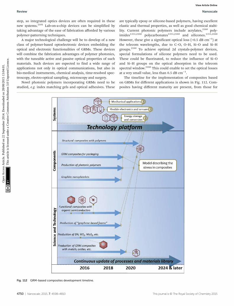
step, so integrated optics devices are often required in thesenew systems.2181 Lab-on-a-chip devices can be simplified bytaking advantage of the ease of fabrication afforded by variouspolymer-patterning techniques.
A major technological challenge will be to develop of a newclass of polymer-based optoelectronic devices embedding theoptical and electronic functionalities of GRMs. These deviceswill combine the fabrication advantages of polymer photonics,with the tuneable active and passive optical properties of suchmaterials. Such devices are expected to find a wide range ofapplications not only in optical communications, but also inbio-medical instruments, chemical analysis, time-resolved spec-troscopy, electro-optical sampling, microscopy and surgery.
Novel photonic polymers incorporating GRMs need to bestudied, e.g. index matching gels and optical adhesives. These
are typically epoxy or silicone-based polymers, having excellentelastic and thermal properties, as well as good chemical stabi-lity. Current photonic polymers include acrylates,2160 poly-imides1353,2160 polycarbonates1353,2160 and silicones.1353,2160
However, these give a significant optical loss (>0.5 dB cm−1) atthe telecom wavelengths, due to C–O, O–H, Si–O and Si–Hgroups.2160 To achieve optimal 2d crystals-polymer devices,special formulations of silicone polymers need to be used.These could be fluorinated, to reduce the influence of Si–Oand Si–H groups on the optical absorption in the telecomspectral window.2160 This could enable to set the optical lossesat a very small value, less than 0.5 dB cm−1.
The timeline for the implementation of composites basedon GRMs for different applications is shown in Fig. 112. Com-posites having different maturity are present, from those for
Fig. 112 GRM-based composites development timeline.
Review Nanoscale
4750 | Nanoscale, 2015, 7, 4598–4810 This journal is © The Royal Society of Chemistry 2015
Ope
n A
cces
s A
rtic
le. P
ublis
hed
on 2
2 Se
ptem
ber
2014
. Dow
nloa
ded
on 2
8/08
/201
5 13
:04:
01.
Thi
s ar
ticle
is li
cens
ed u
nder
a C
reat
ive
Com
mon
s A
ttrib
utio
n 3.
0 U
npor
ted
Lic
ence
.View Article Online
structural applications, already at commercial level and pro-duced in large scale, to graphene-based foams and compositeswith non graphene-2d materials, which might have interestingapplications for flexible electronics and energy storage, but arestill at the fundamental research level. The main targets are:3 years: Functional composites for packaging; Hybrid compo-sites. 3–7 years: Large scale production graphene nanoplatelets7–10 years: GRMs functional composites for mechanical,photonic and energy applications.
12. Biomedical applications
The application of nanotechnology for treatment, diagnosis,monitoring and control of biological systems is called “nano-medicine”.2182 NPs offer unique properties as drug deliverysystems, and image agents.2183 They could also enable one tocombine the diagnostic process with therapy (theranostics).Several NPs are available, ranging from polymeric and metallicones, to liposomes, dendrimers, microcapsules, etc. All ofthese systems are currently under development.2184
GRMs have recently attracted much attention for their poten-tial use in nanomedicine and biology.2185 A common approachfor covalent functionalization of graphene employs GO, whichoffers a new class of solution-dispersible polyaromatic platformfor performing chemistry. The presence of the functional groupsmakes GO hydrophilic,703 allowing its dispersion in water.690
Moreover, the functional groups allow GO to interact with a widerange of inorganic and organic species in non-covalent, covalentand ionic manner, so that functional hybrids can be syn-thesized.2186 Furthermore, in contrast to pure graphene, GO isfluorescent over a broad range of wavelengths.689,2187 This tune-able fluorescence was used in biological applications forsensing2188,2189 and drug delivery.564 Additional chemical proces-sing and modification should continue towards this end.
Research on graphene for biomedical applications is pro-gressing quickly due to the previous know-how gained onCNTs,2190 since the surface chemistry is adaptable from onesystem to the other. Both materials show similar behaviour,with graphene providing additional functionalities withrespect to CNTs, e.g. an enhanced loading of biomolecules,due to its 2d shape.2191
Current challenges include the controlled chemicalfunctionalization of graphene with functional units to achieveboth good processability in various media, and fine tuning ofvarious physico-chemical properties. One aim of the controlledsurface oxidation is the production of anchoring points foradditional surface groups targeting: (1) attachment of bio-molecules (peptides, DNA, growth factors…) via carboxylgroups: KOH/NaOH activation to induce carboxylic acid func-tional groups; (2) PEG coatings to get prolonged blood circula-tion half-life and avoid agglomeration; (3) Sulfonation; (4)Halogenation: fluorination changes the surface hydrophobi-city, while surface bromination provides a starting point forconversion into other functional groups, such as amines, ani-lines, alcohols, or thiols.2192
GO provides a robust framework in which two or more com-ponents can be incorporated to give multifunctional capabili-ties.2193 E.g., the conjugation of multiple components such asfluorescent molecules, tumour-targeting moieties, anticancerdrugs or small interfering Ribonucleic acid (RNA) to GO rep-resents a viable strategy not only to target human cancer, butalso for imaging from inside the body by magnetic resonanceor fluorescent imaging. The ability to simultaneously imageand treat tumours with nanocarriers may provide advantagesover conventional chemotherapies with the added value ofreducing secondary effects. Nanocarriers are considered asmolecular transporters to shuttle various types of biologicalmolecules, including drugs, proteins, DNA, RNA, into cells byendocytosis.
All materials intended to be used in nanomedicine must becarefully tested and their potential effects on cells, animalsand environment investigated.
The small size and the tuneable surface chemistry ofgraphene flakes allows them to efficiently interact with cells,be injected and diffuse further into tissues and into andthrough individual cells. Thus, in this respect, particle sizeis a key parameter. Indeed, size and shape control particleflow and cell internalization.2194 Graphene sheets may flowalong capillaries, lymphatics or tumour vessels withoutobstructions. Flow will also be dependent on surfacefunctionalization; aggregation of flakes should be avoided atany time.
For imaging agents it is essential to have a rapid clearancefrom blood to obtain low background signals and high qualityimages.2195 NPs surface charge and hydrodynamic diameter inpresence of plasma proteins are important for their bio-distri-bution, excretion and rapid clearance from blood.2195
Size control and/or size separation of various scales isnecessary to interface with biological systems in vitro or in vivo.Ultracentrifugation and filtering are the common ways tocontrol size.35,250,642
Graphene has also potential in applications related to bio-sensing and bioelectronics. In particular, μ, together withchemical stability and low electronic noise,2196 offer an excel-lent platform for the development of FET-based biosen-sors.2197 Whereas μ has a direct influence on the devicesensitivity by controlling the intrinsic transistor amplifica-tion,2196 the low noise observed in GFETs (down to 10 µVrms)2196 enables the detection of small electrical and chemicalsignals. The modification of the transistor’s active area withfunctional groups and biomolecules (DNA, enzymes, anti-bodies, etc.) might allow for the development of sensorsspecific to particular analytes, which can find use in ap-plications related to drug screening, proteomics, andgenomics.
GFETs have also attracted attention for their potential usein bioelectronics, in particular for interfacing living cells andnerve tissue.2198 Further, the combination of excellent elec-tronic properties, chemical stability, biocompatibility, andfacile integration with flexible technology, makes graphene acandidate material platform for the next generation of neuro-
Nanoscale Review
This journal is © The Royal Society of Chemistry 2015 Nanoscale, 2015, 7, 4598–4810 | 4751
Ope
n A
cces
s A
rtic
le. P
ublis
hed
on 2
2 Se
ptem
ber
2014
. Dow
nloa
ded
on 2
8/08
/201
5 13
:04:
01.
Thi
s ar
ticle
is li
cens
ed u
nder
a C
reat
ive
Com
mon
s A
ttrib
utio
n 3.
0 U
npor
ted
Lic
ence
.View Article Online
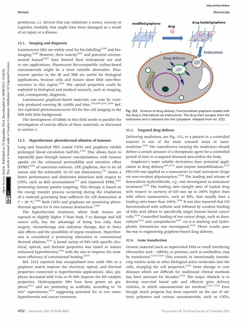
prostheses, i.e. devices that can substitute a motor, sensory orcognitive modality that might have been damaged as a resultof an injury or a disease.
12.1. Imaging and diagnosis
Luminescent QDs are widely used for bio-labelling2199 and bio-imaging.2200 However, their toxicity2201 and potential environ-mental hazard2202 have limited their widespread use andin vivo applications. Fluorescent bio-compatible carbon-basednanomaterials might be a more suitable alternative. Fluo-rescent species in the IR and NIR are useful for biologicalapplications, because cells and tissues show little auto-fluo-rescence in this region.2203 The optical properties could beexploited in biological and medical research, such as imaging,and, consequently, diagnosis.
Luminescent graphene-based materials can now be routi-nely produced covering IR, visible and blue.328,689,2187,2204 Ref.564 exploited photoluminescent GO for live cell imaging in theNIR with little background.
The development of GRMs in this field needs to parallel theinvestigation of toxicity effects of these materials, as discussedin section 3.
12.2. Hyperthermia: photothermal ablation of tumours
Long and branched PEG coated CNTs and graphene exhibitprolonged blood circulation half-life.2205 This allows them torepeatedly pass through tumour vascularisation, with tumouruptake via the enhanced permeability and retention effect(EPRE)2206 of cancerous tumours. LPE graphene, due to its 2dnature and the achievable 10–50 nm dimensions,250 shows abetter performance and distinctive behaviour with respect toCNTs, such as RES accumulation574 and improved EPRE,2207
promoting tumour passive targeting. This therapy is based onthe energy transfer process occurring during the irradiationof a material generating heat sufficient for cell destruction atT > 40 °C.2208 Both CNTs and graphene are promising photo-thermal agents for in vivo tumour destruction.2209
The hyperthermia treatment, where body tissues areexposed to slightly higher T than body T to damage and killcancer cells, has the advantage of being less risky thansurgery, chemotherapy and radiation therapy, due to fewerside effects and the possibility of repeat treatment. Hyperther-mia is considered a promising alternative to conventionalthermal ablation.2210 A broad variety of NPs with specific elec-trical, optical, and thermal properties was tested to induceenhanced hyperthermia,2210 with the aim to improve the treat-ment efficiency of conventional heating.2210
Ref. 2212 reported that encapsulated iron oxide NPs in agraphene matrix improve the electrical, optical, and thermalproperties connected to hyperthermia applications. Also, gra-phene decorated with V/Au or Pt NPs improve the NP catalyticproperties. Hydroxyapatite NPs have been grown on gra-phene2213 and are promising as scaffolds, according to “invivo” experiments,2213 suggesting potential for in vivo nano-hyperthermia and cancer treatment.
12.3. Targeted drug delivery
Delivering medicines, see Fig. 113, to a patient in a controlledmanner is one of the main research areas in nano-medicine.2182 The nanodevices carrying the medicines shoulddeliver a certain amount of a therapeutic agent for a controlledperiod of time to a targeted diseased area within the body.
Graphene’s water soluble derivatives have potential appli-cation in drug delivery563,2214 and enzyme immobilization.2215
PEG-GO was applied as a nanocarrier to load anticancer drugsvia non-covalent physisorption.2198 The loading and release ofdoxorubicin hydrochloride, e.g., was investigated as anticancertreatment.2198 The loading ratio (weight ratio of loaded drugwith respect to carriers) of GO was up to 200% higher thanwith others nanocarriers, such as NPs, that usually have aloading ratio lower than 100%.2196 It was also reported that GOfunctionalized with sulfonic acid followed by covalent bindingof folic acid allows to specifically target human breast cancercells.2216 Controlled loading of two cancer drugs, such as doxo-rubicin2214 and camptothecin2217 via π–π stacking and hydro-phobic interactions was investigated.2216 These results pavethe way to engineering graphene-based drug delivery.
12.4. Gene transfection
Genetic material (such as supercoiled DNA or small interferingribonucleic acid – siRNA), or proteins, such as antibodies, maybe transfected.2218–2220 This consists in intentionally introdu-cing nucleic acids or other biological active molecules into thecells, changing the cell properties.2221 Gene therapy to curediseases which are difficult for traditional clinical methodshas been pursued for decades.2222 The major obstacle is todevelop non-viral based safe and efficient gene deliveryvehicles, in which nanomaterials are involved.2223–2226 Eventhough much progress has been reported on the use of cat-ionic polymers and various nanomaterials, such as CNTs,
Fig. 113 Scheme of drug delivery. Functionalized graphene loaded withthe drug is internalized via endocytosis. The drug then escapes from theendosome and is released into the cytoplasm. Adapted from ref. 2211.
Review Nanoscale
4752 | Nanoscale, 2015, 7, 4598–4810 This journal is © The Royal Society of Chemistry 2015
Ope
n A
cces
s A
rtic
le. P
ublis
hed
on 2
2 Se
ptem
ber
2014
. Dow
nloa
ded
on 2
8/08
/201
5 13
:04:
01.
Thi
s ar
ticle
is li
cens
ed u
nder
a C
reat
ive
Com
mon
s A
ttrib
utio
n 3.
0 U
npor
ted
Lic
ence
.View Article Online

silica NPs and nanodiamonds, as gene deliveryvehicles,2223–2228 a lot more effort is still demanded to developnon-toxic nano-vectors with high gene transfection efficiencyfor potential gene therapy.
GO bound with cationic polymers, such as polyethylene-imine (PEI), was used as nano-vehicle for gene transfection.2229
Cellular toxicity tests revealed that GO-PEI complexes exhibitsignificantly reduced toxicity to the treated cells compared tobare PEI.2229 Positively charged GO-PEI complexes are able tofurther bind with plasmid DNA (pDNA) for intracellular trans-fection of the enhanced green fluorescence protein (EGFP)gene in HeLa cells,2229 isolated for the first time from the cer-vical cancer2230 of Henrietta Laks (HeLa). While EGFP transfec-tion with PEI appears to be ineffective,2229 high EGFPexpression is observed using the corresponding GO-PEI as thetransfection agent.2229 On the other hand, GO-PEI showssimilar EGFP transfection effectiveness, but lower toxicity com-pared with PEI.2229 The first results2229 suggest graphene to bea novel gene delivery nano-vector with low cytotoxicity andhigh transfection efficiency, promising for applications in non-viral based gene therapy.
Whether and how the structure of graphene (e.g. size, thick-ness) would affect the gene transfection efficiency, however,remains an important question that requires further investi-gation. Small interfering ribonucleic acid with therapeuticfunctions may also be delivered by graphene complexes intocancer cells for potential gene therapy. This could be furthercombined with graphene-based chemotherapy and photo-thermal therapy, already demonstrated574,2214,2231 for thedevelopment of multimodal therapies of cancer.
12.5. Bioelectronics and biosensors
The integration of electronics with biological components isone of the current challenges on the path towards bioelectro-nics, which holds great promise for developing prostheses forill or injured organs, as well as leading to a fundamentalunderstanding of the brain.
Biology and electronics may interface at three levels: mole-cular, cellular and skeletal. For any implanted bioelectronicmaterial, the initial interactions at the bio-molecular level willdetermine long-term performance. While bioelectronic is fre-quently associated with skeletal level enhancements (e.g. artifi-cial muscles), electronic communication with living cells is ofinterest for tissue engineering or for implants such as bioniceyes2232 or ears.2233
In the quest towards bioelectronics, different materialswere proposed and investigated. The operation in physiologicalmedia demands special material properties,568 such as electro-chemical stability, biocompatibility, and electronic and chemi-cal functionality. Metals, Si and GaAs and carbon-basedmaterials are expected to provide considerable advantages.Graphene offers a unique combination of physical, chemicaland electronic properties, which may allow it to surpassthe state-of-the-art for bioelectronics and biosensorapplications.568,2234–2236 Indeed, graphene is impervious to theharsh ionic solutions found in the human body.2237 Moreover,
graphene’s ability to conduct electrical signals means it caninterface with neurons and other cells that communicate bynerve impulse, or action potential.2237 These features make itpromising for next-generation bionic technology.568,2237
Current research in nano-biosensors is experiencing a fastgrowth due to the wide range of novel applications for humanhealthcare. A biosensor combines a biological component witha physicochemical detector component and is designed for thedetection of a certain analyte. Biosensors are used for sensitiveand selective detection of biologically-relevant molecules, withapplications in diagnosis (e.g. for the detection of cancer bio-markers), biomedical research, food quality control andenvironmental monitoring.2238
Since Si stability2239,2240 is rather low (i.e. Si oxidizes byinteracting with atmospheric oxygen and organic solutions, orby hydrolysis with aqueous solutions, to give a SiO2 surface),the possible use of Si transistors in the human body requirescoating with metal oxide (e.g. Ir oxide2241) to boost their stabi-lity.2237 Thus, other semiconductor technologies are alsoexplored, such as GaN,2242 SiC2243 and diamond.2244–2246 Thereis however an ever increasing interest in flexible biosen-sors.2247 Another objective is to increase the device intelligenceby integrating computation and decision power.
The use of graphene in biosensors may allow the develop-ment of flexible sensors, as well as improvement of impedanceand biocompatibility, with a high added value. Graphenecould also be used to implement grids of switches to controlmulti-array biosensors or integrate computing/decision power.The main applications are health, medical, pharmaceutical,impedance sensors, DNA chips, bio-labs on chip, bio-monitor-ing, and biomedical calibration.
This field requires transferable SLG or FLGs. Graphene onSiC could be also used, but is not appropriate if flexibledevices are required. Good electrical properties, such as high μand low electronic noise, are compulsory for applications inwhich very small signals are expected (below 100 µV), such asultra-high sensitive biosensor991 or transistors for recordingthe electrical activity of nerve cells.2248 For less demandingapplications, such as electrochemical detection of analytes forfood and environmental monitoring,2249 the performance ofother graphene materials (GO, graphene inks, etc.) might besufficient.
The challenges for the development of ultra-sensitive gra-phene sensors on flexible substrates are many, but the impactof such technology could be even greater. Part of the technol-ogy challenges are similar to those shared by other appli-cations of graphene. Amongst others, they include thepreparation of high quality graphene films, novel concepts forsurface nanostructuring using top-down semiconductor tech-nology as well as nanopatterning with biomolecules based on(bottom-up) chemistry, etc. Other challenges are related tocontact optimization (with a major impact on device perform-ance) and passivation optimization (related to device stability).Further, novel functionalization and biofunctionalizationmethods have to be developed to control the selectivity of thegraphene surface to different analytes. Such methods, which
Nanoscale Review
This journal is © The Royal Society of Chemistry 2015 Nanoscale, 2015, 7, 4598–4810 | 4753
Ope
n A
cces
s A
rtic
le. P
ublis
hed
on 2
2 Se
ptem
ber
2014
. Dow
nloa
ded
on 2
8/08
/201
5 13
:04:
01.
Thi
s ar
ticle
is li
cens
ed u
nder
a C
reat
ive
Com
mon
s A
ttrib
utio
n 3.
0 U
npor
ted
Lic
ence
.View Article Online

might be based on the modification of graphene, should notbe detrimental for the electronic properties of this material.
One of the future targets is bidirectional communication(recording and stimulation) with neurons and nerve tissue,which should enable the study of how a neuronal networkreacts and modifies itself. One goal of such research could beneural prostheses that augment or restore damaged or lostfunctions of the nervous system. The development of brainimplants on flexible substrates, which can record the electricaland chemical activity of neurons, is fundamental for theseapplications. Primary adult retinal ganglion cells were shownto survive on CVD graphene even without any supporting gliallayer (which serves as support cell for the neurons of theretina) or protein coating.2250 This, combined with the out-standing gate-sensitivity performance of solution-gated GFETs(exhibiting a transconductance two orders of magnitude largerthan Si devices568) promises to surpass the state of the art tech-nology for brain implants. Most current implants are based onmetal electrodes.568 However, in addition to some issues withbiocompatibility and stability under the harsh environmentconditions of in vivo implants, metal electrodes do not offerthe intrinsic FET amplification function.568 GFETs, on theother hand, can provide additional advantages due to theinherent amplification function of the FETs, such as animproved signal-to-noise ratio. Variations of the electrical andchemical environment in the vicinity of the FET gate regioncan be converted into a variation of the transistor current. Gra-phene can be employed to fabricate arrays of transistors568 todetect the electrical activity of electrogenic cells (i.e. electricallyactive cells, see Fig. 114), overcoming some of the limitationsof the Si technology, such as the relatively high electric noise(typically, Si-based FETs exhibit an root mean square gatenoise of few tens of microvolts, originating from trapping–detrapping processes at the Si/oxide interface2251) and the inte-gration with flexible substrates. Moreover, Si-based materialsare not stable under physiological conditions.2252,2253
Other important challenges for bioelectronics and biosen-sor applications are the fabrication and in electrolyte character-ization of graphene-based nanoelectrode arrays, theunderstanding of fundamental physical (and chemical) para-meters, such as the impact of the Debye screening in reachingan ultimate precision in detecting the dynamics of chemical
and biological systems, defining a proper biointerface thatwould be compatible with graphene and with a biologicalenvironment, extensive electrophysiology characterization ofthe electrical and chemical graphene/cell synapse, etc.
Future targets are the development of graphene-based bio-electronics and biosensor devices on a flexible substrates, suchas parylene and kapton, already used for in vivo implants.568
Such graphene-based flexible devices might be exploited forthe development of brain implants.2237 Moreover, studiescould be conducted towards the realization of an artificialretina based on flexible GFET array, see Fig. 115.
Degenerative retinal diseases, like retinitis pigmentosa andage-related macular degeneration, are amongst the mostcommon origins of blindness.2254,2255 Electronic visual pros-theses are a prospective therapeutic option of increasingimportance in otherwise incurably impaired patients.2255
Several devices were tested in animal experiments and, accord-ing to the placement of the electrodes, possible stimulationsites are located subretinally,2256 epiretinally,2257 along theoptic nerve,2255 or cortically.2255 The idea is to implant elec-trode arrays in the retina to inject current to the still-functionalneural cells. Electrical patterns corresponding to visual imagescan then be created, and the brain can interpret them asvision.2254,2255 Anatomical, physiological and pathophysiologi-cal aspects must be considered.2254,2255 The optimal inte-gration of the prosthesis into the highly complex system of thevisual pathway is fundamental to provide an appropriateretinal substitute. In this context, a major challenge needs tobe overcome: how to build implants which adapt to the eye’scurvature.2258 This is necessary to prevent unwanted cellgrowth beneath the implant, other than being critical for good
Fig. 114 Schematic GFET with a cardiomyocyte cell (a cell of musculartissue in the heart) on the gate area. The metal contacts (in brown) areinsulated from the electrolyte by two layers of chemically stable andbiocompatible SU8 photoresist (blue rectangles). [Adapted from ref.568].
Fig. 115 Concept for an artificial retina based on a flexible GFETarray.2197
Review Nanoscale
4754 | Nanoscale, 2015, 7, 4598–4810 This journal is © The Royal Society of Chemistry 2015
Ope
n A
cces
s A
rtic
le. P
ublis
hed
on 2
2 Se
ptem
ber
2014
. Dow
nloa
ded
on 2
8/08
/201
5 13
:04:
01.
Thi
s ar
ticle
is li
cens
ed u
nder
a C
reat
ive
Com
mon
s A
ttrib
utio
n 3.
0 U
npor
ted
Lic
ence
.View Article Online

focus. Also, curved implants provide larger areas which can inturn capture larger images.2259
Because graphene is so thin, it could improve the interfacebetween retinal implants and eye tissues. Graphene could bean ideal platform to tackle many other technical challenges.More efficient wireless data and energy supply, combined withdecreasing space requirements, longer durability andincreased safety are required.2255 Moreover, for high resolu-tion, extremely small and densely mounted electrodes areneeded. From today’s perspective it is unclear in whichapproach graphene will lead to the best functional long-termresults. However, it may be assumed that there will not be onesingle universal solution and the specific adjustment of amethod to a particular disease will be fundamental.2255
12.6. Thin films, joint prostheses
Some medical applications require hydrophobic materials witha non-cell adhesive surface, such as devices in contact withhuman blood (e.g. artificial heart valves) or joint prostheses inthe friction area, while others need a cell-adhesive surface toassure complete tissue integration of the implanted materialin the human body. Graphene may be another possibility asbiocompatible coating together with other carbon layers, suchas nano-diamond coatings2260 or DLC.2261 For this purpose,graphene-inks deposition techniques, as well as growth onmetals, should adapt to have a competitive cost and be able tocover large and complexes surfaces. Graphene could be usefulas coating of medical tools. However, this research area is stillat the beginning, with huge improvement needed.2262,2263
Graphene might also be used as reinforcement for poly-meric and ceramic prostheses. Small percentages of grapheneor GO improve polymer elongation at break,2264 leading totougher materials.2264 These graphene-based polymer compo-sites can also exhibit good tribological properties,2264 the start-ing point towards the realization of prostheses.2264
12.7. Single-molecule genomic screening devices
The translocation of proteins and DNA through nanopores isbecoming a key tool for the detection of single mole-cules.2265,2266 Nanopores – nanosized holes that can transportions and molecules – are very promising for genomic screen-ing, in particular DNA sequencing,2267 by rapid electronicdetection of the base sequence of single DNA molecules. DNAsequencing is rapidly growing into an industry of major inter-est. A variety of ‘conventional’ techniques exist, each with theirown pros and cons.2268 The idea of using nanopores for DNAsequencing was proposed over 20 years ago.2269 The firstexperimental proof of translocation of DNA molecules wasreported in 1996 using the biological protein pore α-hemo-lysin,2270 albeit without sequence information. It has taken sig-nificantly more time to establish that single nucleotides canbe discriminated within the traversing DNA, most prominentlybecause the speed of translocating DNA has been too fast (∼μsper base) to identify individual bases.2271 In theory, the basicidea of nanopores sequencing is straightforward: pass a DNAmolecule from head to tail through a nanoscale pore in a
membrane, and read off each base when it is located at thenarrowest constriction of the pore, using the ion currentpassing through the pore to probe the identity of the base.
Single-stranded DNA molecules were statically captured in aα-hemolysin nanopore using a DNA hairpin (unpaired loop ina single-stranded DNA – ssDNA)2273 or a protein attached tothe DNA end, either of which are too large to enter the pore.This allowed the detection of single-nucleotide mutations inthe immobilized DNA.2274–2276 Ref. 2277 modified α-hemolysinto include a cyclodextrin ring that binds free mononucleotides,which therefore reside in the pore for long enough (up to10 ms) to be distinguished by ionic current levels for each ofthe four bases.2277
More recently, the use of DNA polymerases (enzymes thatsynthesise DNA) that drive a DNA template through a nano-pore in single-nucleotide steps as DNA is synthesized wassuggested.2278 Ref. 2278 found that certain DNA polymeraseswere potentially suitable to this approach because theyremained bound to DNA, even against the force of an appliedvoltage needed to insert the DNA into the pore. The polymer-ase, which processes DNA at a rate of about one nucleotideevery 10 ms or slower,982 lowered the translocation speed ofDNA by four orders of magnitude compared to freely translo-cating DNA.2278
Other advantages of nanopore sequencing with respect toother techniques include the single-molecule read-out, the factthat multiple molecules can be processed by a single pore, theabsence of expensive fluorophore labelling, and the lack ofamplification steps.
Looking ahead, a number of improvements are needed. Theerror rate must be decreased (a 4% error rate was reported inref. 2279), the read length needs to be increased further, andthe stability of the protein pores over time needs improvement.Current state of the art solid-state nanopores suffer the draw-back that the channel is long, ∼100 times the distancebetween two bases in a DNA molecule (0.5 nm for ss DNA).E.g., conventional Si-based nanopore membranes are ∼30 nmthick,982 corresponding to ∼60 bases along a ssDNA molecule.They are therefore not directly useful as-is in DNA sequencingapplications, although solid-state nanopores are excellent newtools for biophysical studies.2268
Suspended graphene membranes are ideal for this newclass of sensors, as they are atomically thin, stable, inert, andcan be patterned with atomic resolution,317,2272 Fig. 116(a).
Ref. 980, 2280 demonstrated that ultrathin nanopores fabri-cated in SLG can be exploited to realize single-molecule DNAtranslocation. A small nano-size hole can be drilled into a gra-phene membrane by direct knock-on damage, Fig. 116(b),using the focused electron beam of a TEM,2280,2281 or alterna-tively by a focused ion beam.2282,2283 This membrane is sub-sequently placed between two reservoirs of liquid, and a ioniccurrent can then be measured across the membrane. The tra-versal of single DNA molecules through the hole can be moni-tored as temporal changes in the ionic current,980 Fig. 116(c).As individual DNA molecules translocate through the pore andDNA blocks the path for ionic current, characteristic temporary
Nanoscale Review
This journal is © The Royal Society of Chemistry 2015 Nanoscale, 2015, 7, 4598–4810 | 4755
Ope
n A
cces
s A
rtic
le. P
ublis
hed
on 2
2 Se
ptem
ber
2014
. Dow
nloa
ded
on 2
8/08
/201
5 13
:04:
01.
Thi
s ar
ticle
is li
cens
ed u
nder
a C
reat
ive
Com
mon
s A
ttrib
utio
n 3.
0 U
npor
ted
Lic
ence
.View Article Online

conductance changes are observed in the ionic currentthrough the nanopore, allowing single molecule detection,and setting the stage for future single-molecule genomicscreening devices.980
Ref. 334 formed 12 nm gaps between two graphene electro-des, which act as electrical contacts for molecules that bridgethe gap, see Fig. 117. The devices are stable at RT. This tech-nique could be used to contact a variety of objects (molecules,particles), as well as to explore functionalization of the con-tacts. The graphene electrodes in turn may be contacted by avariety of metals, including ferromagnets, superconductors,etc. Building on the early experiments on DNA transloca-tion,980,2280 sensitivity can be pushed with the ultimate goal ofresolving individual bases in ssDNA. As an alternative tomeasuring ionic currents, devices may be developed based onthe control of tunnelling current between two sheets of gra-phene by the passage of a DNA molecule.
With further optimization of the patterning, i.e. smallerand more consistently shaped holes, the precision and spatialresolution of the process may be further increased. Mild oxi-dation2284 and carbothermal etching2285 processes, sensitive tothe crystal orientation, could be employed to improve the regu-larity of such holes. In concert with corresponding progress inreadout circuitry, as well as modelling, this could lead to con-sistent discrimination between individual base-pairs, there-fore, in turn, sequencing of DNA molecules. A key challenge ishow to progress towards practical fabrication of such sensors,as patterning using TEM or focused ion beams is slow andinconvenient compared to the requirements of large-scalefabrication.
Modelling and data analysis should improve in order to cor-rectly interpret signals from DNA molecules passing throughlarger holes (e.g. 10 nm diameters). Ultrahigh resolution pat-terning strategies with potential for upscaling should be deve-loped, possibly bottom-up, like BC lithography,331 nanosphere
lithography1706 or other types of self-assembled etch masks.Most of these methods, however, are much better suited formaking large arrays of patterns than individual nanopores.While proof-of-concept DNA sequencing is a prime target, thelong-term success of such a technology requires substantialefforts in developing atomic-precision nanopatterning withhigher throughput.
12.8. Plasmonic biosensors
SPR biosensors2290 are currently the most widely used platformfor label-free, real time sensing and monitoring of bio-molecules and molecular reaction events.2290 We can typicallydistinguish two classes: (a) Prism-coupled SPR sensors,2291 uti-lizing propagating SPP on a flat functionalized thin metal film.SPPs are excited at specific angles and wavelengths resultinginto a sharp dip in reflectance (see Fig. 118a). Sensing occursby monitoring the change in resonant angle or wavelengthcaused by adsorbed analytes on the metal surface.
This is the commercial standard providing the best sensi-tivity and proven functionality, at the expense, however, ofnecessitating bulky optical components and alignmentsystems, prohibiting compact, low-cost devices, and high-throughput bioanalytical measurements.
Fig. 116 Nanopore sensors for detecting the translocation of single DNA molecules. (a) Illustration of DNA molecule passing through a nanopore ina suspended SLG. (b) Transmission electron micrograph of a nanopore drilled using an electron beam in (left) MLG and (right) SLG. (c) Conductanceas a function of time (left) before and (right) during translocation of double-stranded DNA across a 22 nm graphene nanopore. The spikes indicateblockage events. Adapted from ref. 980.
Fig. 117 Single-molecule transistor with graphene electrodes [Adaptedform ref. 334].
Review Nanoscale
4756 | Nanoscale, 2015, 7, 4598–4810 This journal is © The Royal Society of Chemistry 2015
Ope
n A
cces
s A
rtic
le. P
ublis
hed
on 2
2 Se
ptem
ber
2014
. Dow
nloa
ded
on 2
8/08
/201
5 13
:04:
01.
Thi
s ar
ticle
is li
cens
ed u
nder
a C
reat
ive
Com
mon
s A
ttrib
utio
n 3.
0 U
npor
ted
Lic
ence
.View Article Online

Recent proposals to overcome this limitation2292,2293
include SPP excitation by nanoholes,2290,2294 nanopits,2295
nanoslits2296 or gratings,2297 with the possibility of utilizingSPP interference in a Mach–Zehnder (MZ) interferometricconfiguration.2298–2300 (b) Nanoplasmonic sensors,2301–2303 uti-lizing localized SPR (LSPRs) in NP assemblies,2304–2306 andmetamaterials,2307,2308 typically excited by normally-incidentcollimated beams. The plasmonic nanostructures exhibitsharp resonances due to LSPRs, and sensing occurs by moni-toring the change in resonance wavelength caused by analytesadsorbed on the nanostructured metal surface (see Fig. 118b).This configuration enables an imaging scheme for a low-cost,miniaturized, high-throughput on-chip biosensing platform.With careful tuning and optimization of the metal nano-structures, nanoplasmonic sensors can surpass the perform-ance levels of state of the art commercial prism-coupled SPRsensors,2309 offer single molecule detection2305,2306 with label-free biosensing methods.2310
Graphene has several properties that could enhancebiosensing: intrinsic plasmons in the IR to THz rangewith high field concentration252,1321,1326 and long life-time,1321,1579,1580 constant absorption in visible to IR,990 highbiomolecule functionalization capability due to π-stackinginteractions,2311–2313 low small molecule permeability offeringpassivation against corrosion.2062,2314,2315 In particular, gra-phene can provide new perspectives in plasmonic sensing inthree main ways: (1) as a functional surface, which supportsintrinsic surface plasmons at IR frequencies: SPPs in bulk andLSPRs in nanostructured graphene, (2) as a functional gate-tuneable coating for existing plasmonic devices: functionali-zation of Au and Ag surfaces (bulk or nanostructured), LSPRcontrol and tuning via gating, protection against corrosion forAg and Cu2339 (3) as a direct transducer eliminating the needfor optical detection.
The vision for graphene-based plasmonic sensing in 10years and beyond is the development of a low-cost, ultra-sensi-tive, ultra-compact, label-free, on-chip, high-throughput andrealtime sensing platform.
12.8.1. Utilizing graphene’s intrinsic plasmons. Graphenesupports gate-tunable plasmon modes in MIR and FIR.448
These consist of propagating SPP modes in graphene252,1326
and localized LSPR modes in nanodisks1579 and NRs.1580
LSPRs are tunable by the ribbon width1580 and through gra-phene stacking configurations.1579 Graphene plasmon modesexhibit large confinement252,1326 and long lifetime,1579,1580
much greater than their metallic counterparts. This, whencombined with the functionalization versatility of graphene,makes them an ideal platform for sensing.
Utilizing the intrinsic plasmons of graphene for biosensinghas not yet been demonstrated. Theoretically, a high-indexprism coupling system to match the incident wave’s wavevectorlateral component to the SPP wavevector, either in Kretsch-mann geometry (prism in contact with graphene, seeFig. 118a)2287,2288 or Otto geometry (prism at subwavelengthseparation from graphene and coupling via attenuated totalreflection),2309,2316 could be adequate in exciting THz SPPs inhighly-doped SLG or FLG.2317 Additionally, graphene LSPRscan be used either in an index sensing setup,2318 i.e. measur-ing the reflection or transmission spectrum shift when bio-molecule binding events that change the local environmentoccur on their surface or, in a surface-enhanced infraredabsorption (based on the enhancement of the IR absorption oforganic molecules in proximity of noble metal substrates)(SEIRA2319–2321) setup, where the LSPR is tuned to the analyte’smolecular vibration modes and serves as a substrate forenhanced absorption.2318 For SEIRA, the possibility ofdynamic tuning the LSPR frequency may enable simultaneousmultimode detection. Finally, SPPs excited on GNR waveguidesand waveguide pairs1325 could be used in a MZ interferometricsetup.
12.8.2. Graphene as a functionalization-passivation gate-tuneable coating. Graphene can be used as a functionalizationelement on top of Au films in a standard bulk SPR sensorsetup.2310 A key property is its ability to stably adsorb bio-molecules via π-stacking interactions, without compromisingAu conductivity.2311–2313
A performance improvement factor of (1 + 0.0025Nψ) wasestimated,2322 where ψ > 1 is the ratio of the number of bio-molecules adsorbed on the graphene/Au surface to thoseadsorbed on a bare Au surface. Graphene was also shown tosignificantly modify the LSPR of Au nanorods when placed ontop of them,2323 making their optical response particularly sen-sitive to charge transfer events,2323 theoretically down to singlecharge transfer events.2323 SPPs on Ag films and LSPRs onnanostructured Ag exhibit a sharper response curve and canthus offer superior sensitivity compared to Au.2324 The mainproblem of Ag as a sensing platform is its low resistance to sul-fidation (introduction of sulfide ions in a material),2325,2326
detrimental to the plasmonic response.2326 Graphene’s imper-meability to small molecules is a viable solution for Ag surfacepassivation2327 (see Fig. 119a), which, when combined withgraphene’s ease of functionalization, may enable Ag-based bio-sensing.2328,2339 At the same time, graphene-protected Cu sur-vives in air and water environments, provides much better
Fig. 118 (a) Scheme of a prism-coupled SPR biosensor in the Kretsch-mann configuration (where a thin metallic layer is formed on the sub-strate and acts itself as the spacer).2286 A high-index prism is used tomatch the incident wave’s wavevector lateral component to the SPPwavevector.2287,2288 (b) Scheme of a nanoplasmonic biosensor. Functio-nalized nanoparticles can be simultaneously interrogated within anoptical imaging approach. Adapted from ref. 2290, 2289.
Nanoscale Review
This journal is © The Royal Society of Chemistry 2015 Nanoscale, 2015, 7, 4598–4810 | 4757
Ope
n A
cces
s A
rtic
le. P
ublis
hed
on 2
2 Se
ptem
ber
2014
. Dow
nloa
ded
on 2
8/08
/201
5 13
:04:
01.
Thi
s ar
ticle
is li
cens
ed u
nder
a C
reat
ive
Com
mon
s A
ttrib
utio
n 3.
0 U
npor
ted
Lic
ence
.View Article Online

phase sensitivities for SPR detection compared to Au, sustainsnano-fabrications and opens a field of graphene-protected Cu-based plasmonics.2339
Metamaterials based on subwavelength MNP assembliescan be tuned to provide narrow optical resonances,2329–2331
important for increased sensitivity. Graphene on top of a meta-material works as a functionalization layer, allowing theadsorption of biomolecules close to the metamaterial surface.Such a scheme was demonstrated with split-ring resonators2332
and diffractively coupled NP arrangements that yield topologi-cally protected zero reflection [i.e. the metamaterial’s effectiveindex as a function of frequency crosses the zero-reflection lineon the complex index (n, k) plane, whereby there is always afrequency at which zero-reflection is obtained irrespective ofstructure imperfections or variations] accompanied by phasesensitivity, measured through an ellipsometric setup2310 (seeFig. 119b). In the latter case, the sensitivity can be better than1 fg mm−2 (ref. 2310), over 3 orders of magnitude better thanstate-of-the-art SPR sensors,2291 and within the realm of label-ling methods, making this the ultimate SPR-biosensorplatform.
12.8.3. Graphene as a direct transducer. Interference ofSPPs in a MZ interferometric setup could be used in biosen-sing.2299,2300 The SPPs may be optically excited through sub-wavelength slits, grooves or gratings. E.g., they may be excitedby a single slit on both sides of the Au film (top andbottom)2299 (see Fig. 120a) or by different groves on the sameside of the Au film.2300
After excitation, the SPPs propagate towards another slitwhere they interfere. Dielectric environment changes causephase differences between the two interfering SPP waves,which are recorded in the far field radiation.2299,2300 Refractiveindex sensitivities of 3500 nm RIU−1 (i.e. SPP wavelength shiftper refractive index unit change), just 4 times lower than com-mercial prism-based SPR sensors, have been reported.2291 Inall cases the interference is optically monitored through amicroscope objective.
Besides its use as a passivation and functionalizationcoating on one of the MZ arms, graphene can find novel func-
tionality as a direct transducer. Ref. 2333 proposed a schemesimilar to graphene-based PDs,446,1433 which eliminates theneed for optical detection and enables an ultra-compact inte-gratable sensing platform. Graphene-based transduction ofoptical signal for biodetection was reported with a dielectricwaveguide sensing scheme.2334
Ref. 2333 proposed a grating for SPP excitation, afterwhich the plasmons propagate towards a graphene-coveredslit where they independently interfere with the incomingwave.
The two MZ arm lengths are asymmetric to enable a netphotovoltage response, and fine-tuned for maximal sensitivity.Further extensions to this scheme include graphene for func-tionalizing one or both of the sensor arms, and a MZ schemethat removes the need of the metal and utilizes intrinsic IRplasmons in graphene ribbon waveguides.
Fig. 121 shows the timeline for biosensing and biomedicalapplications.
13. Conclusions
The field of graphene, related 2d crystals and hybrids is nowrapidly evolving from pure science to technology. Differentapplications require GRMs with diverse properties, from struc-turally perfect and high μ graphene for high tech electronics,to defective materials for energy applications, e.g. batteries andsupercapacitors.
The current and near future market for GRM applications isdriven by the production strategies for these materials. Onceeach production route is mature enough, this will enablea widespread practical implementation of these materials.
Fig. 119 (a) Illustration of graphene-passivated Ag nanoantennas fabri-cated in a square array. The graphene layer prevents the reaction oftrace atmospheric hydrogen sulfide (H2S) and carbonyl sulfide (OCS)with the Ag surface. Adapted from ref. 2327. (b) Scheme of a squarearray of Au double-dots on a glass substrate covered by hydrogenatedgraphene. Adapted from ref. 2310.
Fig. 120 (a) Schematic plasmonic MZ interferometer. Adapted from ref.2299. (b) Schematic plasmonic interferometer using grating couplingand an integrated graphene transducer.
Review Nanoscale
4758 | Nanoscale, 2015, 7, 4598–4810 This journal is © The Royal Society of Chemistry 2015
Ope
n A
cces
s A
rtic
le. P
ublis
hed
on 2
2 Se
ptem
ber
2014
. Dow
nloa
ded
on 2
8/08
/201
5 13
:04:
01.
Thi
s ar
ticle
is li
cens
ed u
nder
a C
reat
ive
Com
mon
s A
ttrib
utio
n 3.
0 U
npor
ted
Lic
ence
.View Article Online

Thus, as summarized in the detailed roadmaps in Fig. 122, theavailability of a product for the end user is strictly dependenton the different pace of the material development. The cheap-est GRMs and with the least stringent requirements could bethe first available on the market, to be used, e.g., in flexibleelectronic devices based on conductive inks, such as flexiblesolar cells, batteries and supercapacitors, while devices
which require the highest, electronic quality grade, such asspin valves, non-volatile memories, will take more time toprogress.
The target is to develop novel applications, planned thanksto each GRM unique properties, rather than try to replaceother materials in existing applications. GRMs will replaceexisting standard materials only if the properties of the new
Fig. 121 Biomedical applications timeline.
Nanoscale Review
This journal is © The Royal Society of Chemistry 2015 Nanoscale, 2015, 7, 4598–4810 | 4759
Ope
n A
cces
s A
rtic
le. P
ublis
hed
on 2
2 Se
ptem
ber
2014
. Dow
nloa
ded
on 2
8/08
/201
5 13
:04:
01.
Thi
s ar
ticle
is li
cens
ed u
nder
a C
reat
ive
Com
mon
s A
ttrib
utio
n 3.
0 U
npor
ted
Lic
ence
.View Article Online

components are amply competitive to justify the cost for chan-ging current industrial processes.
Acknowledgements
We acknowledge useful discussions with A. K. Geim, K. vonKlitzing, S. Haque, C. Kerr, R. Phaal, N. Athanassopoulou,
R. S. Ruoff, G. Yu, M. Stoller, P. Avouris, C. W. J. Beenakker,V. Amendola, M. Meneghetti, L. J. Biró, E. Burovski,G. Calogero, C. P. Grey, M. Lemme, D. Chang, V. Cheianov,Luciano Colombo, M. Dragoman, N. Drummond, R. Dryfe,M. Fogelström, J-C. Gabriel, P. G. Gucciardi, M. G. Donato,C. S. Vasi, P. H. Jones, R. Saija, S. Savasta, T. Hasan,A. Isacsson, M. Inguscio, J. Iwaszkiewicz, U. Jansson,L. Jansen, A.-P. Jauho, V. Raineri, D. Jimenez, S. Kubatkin,
Fig. 122 The STRs follow a hierarchical structure where the strategic level in a) is connected to the more detailed roadmap shown in b). Thesegeneral roadmaps are the condensed form of the topical roadmaps presented in the previous sections, and give technological targets for key appli-cations to become commercially competitive and the forecasts for when the targets are predicted to be met.
Review Nanoscale
4760 | Nanoscale, 2015, 7, 4598–4810 This journal is © The Royal Society of Chemistry 2015
Ope
n A
cces
s A
rtic
le. P
ublis
hed
on 2
2 Se
ptem
ber
2014
. Dow
nloa
ded
on 2
8/08
/201
5 13
:04:
01.
Thi
s ar
ticle
is li
cens
ed u
nder
a C
reat
ive
Com
mon
s A
ttrib
utio
n 3.
0 U
npor
ted
Lic
ence
.View Article Online
G. Lelay, O. M. Maragò, J. Martins, E. McCann, M. Nesladek,P. Papakonstantinou, A. S. Plaut, G. Saracco, W. Strupinski,A. Tzalenchuk, R. Yakimova, C. Coletti, S. Heun, M. Vitiello,V. Tozzini, G. Fiori, R. J. Young, A. Yurgens, A. Zenasni,R. Duffy, M. Bruna, G. Privitera, R. White, A. Liscio,L. Ortolani, P. Samorì, R. Gonnelli, F. Rossi, F. Pirri, M. Vallet-Regi, P. Godignon, E. Diez, F. Calle, M. Lopez-Manchado,R. Menendez, M. Pruneda, A. Cabellos, M. Osendi,J. J. Vilatela, J. Kürti, C. Balázsi, T. Szabó, I. Dékány,A. Virosztek, B. Dora, A. Bacsi, M. Affronte, A. Candini, Ilie,Z. Klusek, A. Gourdon, H. Hod, M. De Sousa, H. M. H. Chong,T. Rawinski, J. Iwaszkiewicz, M. Mogenstern, M. N. Portnoi,S. Bending, M. Massiccotte, H. Rhedin, E. Novoselova,N. Walter, C. Algora, J. A. Martin- Gago, F. Raso, E. Pop, S.Lazcano and A. de Andres. We acknowledge funding by the ECunder the Graphene Flagship Pilot and the Graphene Flagship(grant agreement no. 604391).
References
1 Nanotechnologies for Future Mobile Devices, ed. T. Ryhänen,M. A. Uusitalo, O. Ikkala and A. Kärkkäinen, CambridgeUniversity Press, 2010.
2 http://www.basf.com/group/corporate/chemistryworldtour/en/innovationen/smart-forvision.
3 H. Kroemer, Rev. Mod. Phys., 2001, 73, 783–793.4 K. S. Novoselov, A. K. Geim, S. Morozov, D. Jiang, Y. Zhang,
S. Dubonos, I. Grigorieva and A. Firsov, Science, 2004, 306,666–669.
5 K. S. Novoselov, D. Jiang, F. Schedin, T. Booth,V. Khotkevich, S. Morozov and A. K. Geim, Proc. Natl. Acad.Sci. U. S. A., 2005, 102, 10451–10453.
6 X. Li, W. Cai, J. An, S. Kim, J. Nah, D. Yang, R. Piner,A. Velamakanni, I. Jung, E. Tutuc, S. K. Banerjee,L. Colombo and R. S. Ruoff, Science, 2009, 324, 1312–1314.
7 S. Bae, H. Kim, Y. Lee, X. Xu, J. S. Park, Y. Zheng,J. Balakrishnan, T. Lei, H. Ri Kim, Y. I. Song, Y. J. Kim,K. S. Kim, B. Özyilmaz, J. H. Ahn, B. H. Hong and S. Iijima,Nat. Nanotechnol., 2010, 5, 574–578.
8 A. Kumar and C. Zhou, ACS Nano, 2011, 4, 11–14.9 K. S. Kim, Y. Zhao, H. Jang, S. Y. Lee, J. M. Kim, K. S. Kim,
J. H. Ahn, P. Kim, J. Y. Choi and B. H. Hong, Nature, 2009,457, 706–710.
10 S. Bae, S. J. Kim, J.-H. Ahn and B. H. Hong, Phys. Scr., 2012,T146, 014024.
11 Y.-M. Lin, A. Valdes-Garcia, S.-J. Han, D. B. Farmer,I. Meric, Y. Sun, Y. Wu, C. Dimitrakopoulos, A. Grill,P. Avouris and K. A. Jenkins, Science, 2011, 332, 1294–1297.
12 http://www.itrs.net.13 D.-M. Sun, C. Liu, W.-C. Ren and H.-M. Cheng, Small, 2013,
9, 1188–1205.14 C. Yan, J. H. Cho and J.-H. Ahn, Nanoscale, 2012, 4, 4870.15 J. G. Son, M. Son, K.-J. Moon, B. H. Lee, J.-M. Myoung,
M. S. Strano, M.-H. Ham and C. A. Ross, Adv. Mater., 2013,25, 4723–4728.
16 J. A. Rogers and Z. Bao, J. Polym. Sci., Part A: Polym. Chem.,2002, 40, 3327–3334.
17 A. J. Steckl, IEEE Spectrum, 2013, 50, 48–61.18 C. Lee, X. Wei, J. W. Kysar and J. Hone, Science, 2008, 321,
385–388.19 V. M. Pereira and A. H. Castro-Neto, Phys. Rev. Lett., 2009,
103, 046801.20 NASA Technology Readiness Levels defined at http://esto.
nasa.gov/files/TRL_definitions.pdf.21 https://www.innovateuk.org/documents/1524978/2139688/
High+Value+Manufacturing+Strategy+2012–15/9b7e55f0-ed9a-4efe-89e5–59d13b2e47f7.
22 Market observatory for energy, Key figures, EU commission,2011.
23 S. Wolf, A. Y. Chtchelkanova and D. Treger, IBM J. Res. Dev.,2006, 50, 101–110.
24 I. Zutic, J. Fabian and S. Das Sarma, Rev. Mod. Phys., 2004,76, 323–410.
25 D. E. Nikonov, G. I. Bourianoff and P. A. Gargini, J. Super-cond. Novel Magn., 2006, 19, 497–513.
26 M. N. Baibich, J. Broto, A. Fert, F. N. Van Dau, F. Petroff,P. Etienne, G. Creuzet, A. Friederich and J. Chazelas, Phys.Rev. Lett., 1988, 61, 2472–2475.
27 A. Fert, Rev. Mod. Phys., 2008, 80, 1517.28 W. Y. Kim and K. S. Kim, Nat. Nanotechnol., 2008, 3, 408–
412.29 W. Y. Kim, Y. C. Choi and K. S. Kim, J. Mater. Chem., 2008,
18, 4510–4521.30 L. Brey and H. Fertig, Phys. Rev. B, 2007, 76, 205435.31 A. Rycerz, J. Tworzydło and C. W. J. Beenakker, Nat. Phys.,
2007, 3, 172–175.32 R. Nandkishore, L. Levitov and A. Chubukov, Nat. Phys.,
2012, 8, 158–163.33 D. C. Elias, R. R. Nair, T. M. G. Mohiuddin, S. V. Morozov,
P. Blake, M. P. Halsall, A. C. Ferrari, D. W. Boukhvalov,M. I. Katsnelson, A. K. Geim and K. S. Novoselov, Science,2009, 323, 610–613.
34 R. R. Nair, W. Ren, R. Jalil, I. Riaz, V. G. Kravets, L. Britnell,P. Blake, F. Schedin, A. S. Mayorov, S. Yuan,M. I. Katsnelson, H.-M. Cheng, W. Strupinski,L. G. Bulusheva, A. V. Okotrub, I. V. Grigorieva,A. N. Grigorenko, K. S. Novoselov and A. K. Geim, Small,2010, 6, 2877–2884.
35 Y. Hernandez, V. Nicolosi, M. Lotya, F. M. Blighe, Z. Sun,S. De, I. T. McGovern, B. Holland, M. Byrne, Y. K. Gun’ko,J. J. Boland, P. Niraj, G. Duesberg, S. Krishnamurthy,R. Goodhue, J. Hutchison, V. Scardaci, A. C. Ferrari andJ. N. Coleman, Nat. Nanotechnol., 2008, 3, 563–568.
36 T. Ramanathan, A. A. Abdala, S. Stankovich, D. A. Dikin,M. Herrera-Alonso, R. D. Piner, D. H. Adamson,H. C. Schniepp, X. Chen, R. S. Ruoff, S. T. Nguyen,I. A. Aksay, R. K. Prud’Homme and L. C. Brinson, Nat.Nanotechnol., 2008, 3, 327–331.
37 S. Park, J. An, R. D. Piner, I. Jung, D. Yang, A. Velamakanni,S. T. Nguyen and R. S. Ruoff, Chem. Mater., 2008, 20, 6592–6594.
Nanoscale Review
This journal is © The Royal Society of Chemistry 2015 Nanoscale, 2015, 7, 4598–4810 | 4761
Ope
n A
cces
s A
rtic
le. P
ublis
hed
on 2
2 Se
ptem
ber
2014
. Dow
nloa
ded
on 2
8/08
/201
5 13
:04:
01.
Thi
s ar
ticle
is li
cens
ed u
nder
a C
reat
ive
Com
mon
s A
ttrib
utio
n 3.
0 U
npor
ted
Lic
ence
.View Article Online
38 J. N. Coleman, M. Lotya, A. O’Neill, S. D. Bergin, P. J. King,U. Khan, K. Young, A. Gaucher, S. De, R. J. Smith,I. V. Shvets, S. K. Arora, G. Stanton, H.-Y. Kim, K. Lee,G. T. Kim, G. S. Duesberg, T. Hallam, J. J. Boland,J. J. Wang, J. F. Donegan, J. C. Grunlan, G. Moriarty,A. Shmeliov, R. J. Nicholls, J. M. Perkins, E. M. Grieveson,K. Theuwissen, D. W. McComb, P. D. Nellist andV. Nicolosi, Science, 2011, 331, 568–571.
39 P. Joensen, R. F. Frindt and S. R. Morrison, Mater. Res.Bull., 1986, 21, 457–461.
40 R. G. Dickinson and L. Pauling, J. Am. Chem. Soc., 1923, 45,1466–1471.
41 R. F. Frindt and A. D. Yoffe, Proc. R. Soc. London, Ser. A,1963, 273, 69–83.
42 R. F. Frindt, Phys. Rev., 1965, 140, A535–A538.43 K. S. Novoselov, Rev. Mod. Phys., 2011, 83, 838.44 Z. Li, C. H. Lui, E. Cappelluti, L. Benfatto, K. F. Mak,
G. L. Carr, J. Shan and T. F. Heinz, Phys. Rev. Lett., 2012,108, 156801.
45 http://www.cambridgeip.com/industries/nanotechnology/graphene/.
46 J. Kinaret, A. C. Ferrari, V. Falko and J. Kivioja, ProcediaComput. Sci., 2011, 7, 30–33.
47 P. A. Grünberg, Rev. Mod. Phys., 2008, 80, 1531–1540.48 A. Fert, Angew. Chem., Int. Ed., 2008, 47, 5956–5967.49 E. Hobsbawm, The Age of Revolution: Europe 1789–1848,
Weidenfeld & Nicolson Ltd., 1962.50 H.-G. Elias, Plastics, General Survey, in Ullmann’s Encyclo-
pedia of Industrial Chemistry, Wiley-VCH, Weinheim, 2005,DOI: 10.1002/14356007.a20_543.
51 W. F. McDonough and S.-s. Sun, Chem. Geol., 1995, 120,223–253.
52 J. Adams and D. Pendlebury, Global ResearchReport: Materials Science and Technology, Thomson Reuters,2011.
53 G. Brumfiel, Graphene goes global: Britain’s big bet on gra-phene, Nature News, 2012.
54 Q. Tannock and R. Duffy, Patenting Flatland: Graphene –Exploitation challenges and opportunities, CambridgeIP,2012.
55 See for example P. Stephens, Graphene: Invented in the UK,largely being developed elsewhere, Financial Times, 2012.
56 D. Harfhof, et al., The Strategic Use of Patents and itsImplications for Enterprise and Competition Policies 9–12,2007.
57 C. Shapiro, Navigating the Patent Thicket: Cross-Licenses,Patent Pools and Standard Setting, Berkeley, 2001.
58 http://cambridgeip.com/pressamedia/publications.html.59 E. G. Acheson, Manufacture of Graphite, U.S. Patent
615648, 1896.60 A. Colli, S. A. Awan, A. Lombardo, T. J. Echtermeyer,
T. S. Kulmala and A. C. Ferrari, US 20130162333, 2013.61 O. Rozhin, A. Ferrari and W. I. Milne, US 20100003528,
2010.62 Y. Woo, S. A. Seo, D. Kim and H. Chung, US 20110089403,
2011.
63 T. Kobayashi, EP 2393107, 2013.64 L. Song, A. Zhamu, J. Guo and B. Z. Jang, US 7623340,
2009.65 S. M. Yoon, W. M. Choi, H. J. Shin and J. Y. Choi, EP
2439779, 2014.66 G. Owen, GB 2471672, 2011.67 B. Z. Jang and A. Zhamu, US 20100000441, 2008.68 R. Murphy, O. Rozhin, A. C. Ferrari, J. Robertson and
W. I. Milne, US 20070275230, 2007.69 F. Torrisi, T. Hasan, F. Bonaccorso and A. C. Ferrari,
WO 2014064432 A1.70 H. Andersson, US 20110311029, 2011.71 O. Rozhin, A. Ferrari and W. I. Milne, US 8323789 B2, 2007.72 P. Avouris, M. B. Steiner, M. Engel, R. Krupke, A. C. Ferrari
and A. Lombardo, US 20130107344 A1, 2013.73 H. Lammer, US 20100125013, 2010.74 A. K. Geim and K. S. Novoselov, Nat. Mater., 2007, 6,
183–191.75 E. Fey and E. Rivin, Innovation on demand: New product
development using TRIZ, Cambridge University Press,Cambridge U.K., 2005.
76 Cambridge IP.77 C. S. Min, KR 20120013604, 2012.78 US 20110089403, Electronic device using a two-dimensional
sheet material, transparent display and methods of fabricatingthe same, 2010.
79 B. L. Choi, E. K. Lee, D. M. Whang and B. S. Kim, EP2327661, 2011.
80 E. S. Kim, S. Y. Lee, M. K. Ryu and K. B. Park, EP 2348531,2013.
81 J. S. Shin, S. C. Jun, Y. K. Park, I. S. Song, Y. I. Kim,D. H. Kim and C. S. Kim, US 20110279188, 2011.
82 J. S. Shin, S. C. Jun, Y. K. Park, I. S. Song, Y. I. Kim,D. H. Kim and C. S. Kim, US 20110279188, 2011.
83 KR 20110075402, Circuit board, 2011.84 D. Wei, C. Bower, T. T. Ryhanen and P. Andrew,
US 20120028127, 2012.85 T. Ryhänen and M. Welland, US 8024279, 2011.86 A. Quinn, B. Long, M. Manning and B. Szafranek, EP
2362459, 2011.87 S. Ivanovici, S. Yang, X. Feng and K. Müllen, US
20110268647, 2011.88 S. Ivanovici, S. Yang, X. Feng and K. Müllen, US
20110292570, 2011.89 V. Varma, D. Scheffer, J. C. R. Ginneman and J. S. Lettow,
EP 2414286, 2012.90 I. A. Aksay, D. L. Milius, S. Korkut and R. K. Prud’homme,
EP 2240404, 2010.91 D. H. Adamson, I. A. Aksay, C. D. O’neil, B. Ozbas,
R. K. Prud’homme and R. A. Register, EP 2067146, 2009.92 D. H. Adamson, I. A. Aksay, B. Ozbas, R. K. Prud’homme
and R. A. Register, EP 2070093, 2007.93 J. M. Tour and D. V. Kosynkin, EP 2432733, 2010.94 J. M. Tour, D. V. Kosynkin, A. Duque and K. B. Price, EP
2327085, 2009.95 J. M. Tour and D. V. Kosynkin, EP 2443062, 2010.
Review Nanoscale
4762 | Nanoscale, 2015, 7, 4598–4810 This journal is © The Royal Society of Chemistry 2015
Ope
n A
cces
s A
rtic
le. P
ublis
hed
on 2
2 Se
ptem
ber
2014
. Dow
nloa
ded
on 2
8/08
/201
5 13
:04:
01.
Thi
s ar
ticle
is li
cens
ed u
nder
a C
reat
ive
Com
mon
s A
ttrib
utio
n 3.
0 U
npor
ted
Lic
ence
.View Article Online

96 B. H. Hall, C. Helmers, G. von Graevenitz and C. Rosazza-Bondibene, The Study of Patent Thickets, The IntellectualProperty Office, 2013, ISBN: 978-1-908908-77-3.
97 J. Bessen, Patent Thickets: Strategic Patenting of ComplexTechnologies, 2004.
98 I. Iliev, P. Tang, H. van der Merwe and Q. Tannock, Emer-ging patent thickets and standards in the medical devices andtelehealth space, CambridgeIP, 2011.
99 A. S. Mayorov, R. V. Gorbachev, S. V. Morozov, L. Britnell,R. Jalil, L. A. Ponomarenko, P. Blake, K. S. Novoselov,K. Watanabe, T. Taniguchi and A. K. Geim, Nano Lett.,2011, 11, 2396–2399.
100 J. Baringhaus, M. Ruan, F. Edler, A. Tejeda, M. Sicot,A. Taleb-Ibrahimi, A. P. Li, Z. Jiang, E. H. Conrad,C. Berger, C. Tegenkamp and W. A. de Heer, Nature, 2014,506, 349–354.
101 J. S. Bunch, S. S. Verbridge, J. S. Alden, A. M. Van DerZande, J. M. Parpia, H. G. Craighead and P. L. McEuen,Nano Lett., 2008, 8, 2458–2462.
102 A. A. Balandin, Nat. Mater., 2011, 10, 569–581.103 J. Moser, A. Barreiro and A. Bachtold, Appl. Phys. Lett.,
2007, 91, 163513.104 K. S. Novoselov, Rev. Mod. Phys., 2011, 83, 837–849.105 A. K. Geim and I. V. Grigorieva, Nature, 2013, 499, 419–
425.106 L. Britnell, R. V. Gorbachev, R. Jalil, B. D. Belle,
F. Schedin, A. Mishchenko, T. Georgiou, M. I. Katsnelson,L. Eaves, S. V. Morozov, N. M. R. Peres, J. Leist,A. K. Geim, K. S. Novoselov and L. A. Ponomarenko,Science, 2012, 335, 947–950.
107 H. Yang, J. Heo, S. Park, H. J. Song, D. H. Seo, K.-E. Byun,Ph. Kim, I. Yoo, H.-J. Chung and K. Kim, Science, 2012,336, 1140–1143.
108 C. Zeng, E. B. Song, M. Wang, S. Lee, C. M. Torres,J. Tang, B. H. Weiller and K. L. Wang, Nano Lett., 2013, 13,2370–2375.
109 G. Giovannetti, P. Khomyakov, G. Brocks, V. Karpan,J. Van den Brink and P. Kelly, Phys. Rev. Lett., 2008, 101,26803.
110 P. Avouris, Nano Lett., 2010, 10, 4285–4294.111 J. A. Wilson and A. D. Yoffe, Adv. Phys., 1969, 18, 193–335.112 C. L. Kane and E. J. Mele, Phys. Rev. Lett., 2005, 95,
226801.113 P. Vogt, P. De Padova, C. Quaresima, J. Avila,
E. Frantzeskakis, M. C. Asensio, A. Resta, B. Ealet andG. Le Lay, Phys. Rev. Lett., 2012, 108, 155501.
114 B. Lalmi, H. Oughaddou, H. Enriquez, A. Kara, S. Vizzini,B. Ealet and B. Aufray, Appl. Phys. Lett., 2010, 97, 223109.
115 C. C. Liu, W. Feng and Y. Yao, Phys. Rev. Lett., 2011, 107,076802.
116 H. Liu, A. T. Neal, Z. Zhu, D. Tomanek and P. D. Ye, ACSNano, 2014, 8, 4033–4041.
117 T. Osaka, H. Orni, K. Yamamoto and A. Ohtake, Phys. Rev.B, 1994, 50, 7567.
118 H. Zimmermann, R. C. Keller, P. Meisen andM. Seelmann-Eggebert, Surf. Sci., 1997, 377–379, 904–908.
119 M. Naguib, O. Mashtalir, J. Carle, V. Presser, J. Lu,L. Hultman, Y. Gogotsi and M. W. Barsoum, ACS Nano,2012, 6, 1322–1331.
120 O. Mashtalir, M. Naguib, V. N. Mochalin, Y. Dall’Agnese,M. Heon, M. W. Barsoum and Y. Gogotsi, Nat. Commun.,2013, 4, 1716.
121 G. Savini, A. C. Ferrari and F. Giustino, Phys. Rev. Lett.,2010, 105, 037002.
122 E. Bianco, S. Butler, S. Jiang, O. D. Restrepo, W. Windland J. E. Goldberger, ACS Nano, 2013, 7, 4414–4421.
123 Y. Xu, B. Yan, H.-J. Zhang, J. Wang, G. Xu, P. Tang,W. Duan and S.-C. Zhang, Phys. Rev. Lett., 2013, 111,136804.
124 G. Vogg, M. S. Brandt and M. Stutzmann, Adv. Mater.,2000, 12, 1278–1281.
125 A. K. Geim, Science, 2009, 324, 1530–1534.126 E. McCann and V. I. Fal’ko, Phys. Rev. Lett., 2006, 96,
86805.127 J. B. Oostinga, H. B. Heersche, X. Liu, A. F. Morpurgo and
L. M. K. Vandersypen, Nat. Mater., 2007, 7, 151–157.128 Y. Zhang, T. T. Tang, C. Girit, Z. Hao, M. C. Martin,
A. Zettl, M. F. Crommie, Y. R. Shen and F. Wang, Nature,2009, 459, 820–823.
129 T. M. G. Mohiuddin, A. Lombardo, R. R. Nair, A. Bonetti,G. Savini, R. Jalil, N. Bonini, D. M. Basko, C. Galiotis,N. Marzari, K. S. Novoselov, A. K. Geim and A. C. Ferrari,Phys. Rev. B, 2009, 79, 205433.
130 V. Fal’ko, Nat. Phys., 2007, 3, 151–152.131 N. F. Mott, J. Non-Cryst. Solids, 1968, 1, 1–17.132 A. L. Efros and B. I. Shklovskii, J. Phys. C: Solid State Phys.,
1975, 8, L49.133 B. I. Shklovskii and A. L. Efros, Electronic Properties of
Doped Semiconductors, Springer-Verlag, Berlin, 1984.134 A. C. Ferrari and D. Basko, Nat. Nanotechnol., 2013, 8,
235–246.135 A. C. Ferrari, J. C. Meyer, V. Scardaci, C. Casiraghi,
M. Lazzeri, F. Mauri, S. Piscanec, D. Jiang,K. S. Novoselov, S. Roth and A. K. Geim, Phys. Rev. Lett.,2006, 97, 187401.
136 A. C. Ferrari, Solid State Commun., 2007, 143, 47–57.137 Y. J. Yu, Y. Zhao, S. Ryu, L. E. Brus, K. S. Kim and P. Kim,
Nano Lett., 2009, 9, 3430–3434.138 J. Martin, N. Akerman, G. Ulbricht, T. Lohmann, J. Smet,
K. Von Klitzing and A. Yacoby, Nat. Phys., 2007, 4,144–148.
139 A. Tselev, N. V. Lavrik, I. Vlassiou, D. P. Briggs,M. Rutgers, R. Proksch and S. V. Kalinin, Nanotechnology,2012, 23, 385706.
140 V. V. Cheianov and V. I. Fal’ko, Phys. Rev. B, 2006, 74,041403.
141 M. Katsnelson, K. S. Novoselov and A. K. Geim, Nat. Phys.,2006, 2, 620–625.
142 A. Cresti, N. Nemec, B. Biel, G. Niebler, F. Triozon,G. Cuniberti and S. Roche, Nano Res., 2008, 1, 361–394.
143 V. V. Cheianov, V. Fal’ko and B. Altshuler, Science, 2007,315, 1252–1255.
Nanoscale Review
This journal is © The Royal Society of Chemistry 2015 Nanoscale, 2015, 7, 4598–4810 | 4763
Ope
n A
cces
s A
rtic
le. P
ublis
hed
on 2
2 Se
ptem
ber
2014
. Dow
nloa
ded
on 2
8/08
/201
5 13
:04:
01.
Thi
s ar
ticle
is li
cens
ed u
nder
a C
reat
ive
Com
mon
s A
ttrib
utio
n 3.
0 U
npor
ted
Lic
ence
.View Article Online
144 K. I. Bolotin, K. Sikes, Z. Jiang, M. Klima, G. Fudenberg,J. Hone, P. Kim and H. Stormer, Solid State Commun.,2008, 146, 351–355.
145 X. Du, I. Skachko, A. Barker and E. Y. Andrei, Nat. Nano-technol., 2008, 3, 491–495.
146 K. S. Novoselov, A. K. Geim, S. Morozov, D. Jiang,M. I. K. I. V. Grigorieva, S. Dubonos and A. Firsov, Nature,2005, 438, 197–200.
147 Y. Zhang, J. P. Small, M. E. S. Amori and P. Kim, Phys. Rev.Lett., 2005, 94, 176803.
148 Y. Zhang, Y. W. Tan, H. L. Stormer and P. Kim, Nature,2005, 438, 201–204.
149 K. S. Novoselov, E. McCann, S. Morozov, V. I. Fal’ko,M. Katsnelson, U. Zeitler, D. Jiang, F. Schedin andA. K. Geim, Nat. Phys., 2006, 2, 177–180.
150 K. v. Klitzing, G. Dorda and M. Pepper, Phys. Rev. Lett.,1980, 45, 494–497.
151 X. Du, I. Skachko, F. Duerr, A. Luican and E. Y. Andrei,Nature, 2009, 462, 192–195.
152 K. Bolotin, F. Ghahari, M. D. Shulman, H. L. Stormer andP. Kim, Nature, 2009, 462, 196–199.
153 K. Komatsu, C. Li, S. Autier-Laurent, H. Bouchiat andS. Gueron, Phys. Rev. B, 2012, 86, 115412.
154 A. Tzalenchuk, S. Lara-Avila, A. Kalaboukhov, S. Paolillo,M. Syväjärvi, R. Yakimova, O. Kazakova, T. Janssen,V. Fal’Ko and S. Kubatkin, Nat. Nanotechnol., 2010, 5, 186–189.
155 T. Janssen, A. Tzalenchuk, R. Yakimova, S. Kubatkin,S. Lara-Avila, S. Kopylov and V. Fal’ko, Phys. Rev. B, 2011,83, 233402.
156 K. Iwamoto, Y. Kamimuta, A. Ogawa, Y. Watanabe,S. Migita, W. Mizubayashi, Y. Morita, M. Takahashi,H. Ota, T. Nabatame and A. Toriumi, Appl. Phys. Lett.,2008, 92, 132907.
157 Y. Xuan, Y. Q. Wu, T. Shen, M. Qi, M. A. Capano,J. A. Cooper and P. D. Ye, Appl. Phys. Lett., 2008, 92,013101.
158 O. Leenaerts, B. Partoens and F. M. Peeters, Phys. Rev. B,2009, 79, 235440.
159 I. Meric, M. Y. Han, A. F. Young, B. Ozyilmaz, P. Kimand K. L. Shepard, Nat. Nanotechnol., 2008, 3, 654–659.
160 S. Lara-Avila, K. Moth-Poulsen, R. Yakimova,T. Bjørnholm, V. Fal’ko, A. Tzalenchuk and S. Kubatkin,Adv. Mater., 2011, 23, 878–882.
161 T. Maeda, H. Otsuka and A. Takahara, Prog. Polym. Sci.,2009, 34, 581–604.
162 H. Y. Jeong, J. Y. Kim, J. W. Kim, J. O. Hwang,J.-E. Kim, J. Y. Lee, T. H. Yoon, B. J. Cho, S. O. Kim,R. S. Ruoff and S.-Y. Choi, Nano Lett., 2010, 10, 4381–4386.
163 H. B. Heersche, P. Jarillo-Herrero, J. B. Oostinga,L. M. K. Vandersypen and A. F. Morpurgo, Nature, 2007,446, 56–59.
164 K. Nagashio, T. Nishimura, K. Kita and A. Toriumi, Appl.Phys. Lett., 2010, 97, 143514.
165 S. Russo, M. F. Craciun, M. Yamamoto,A. F. Morpurgo and S. Tarucha, Physica E, 2010,42, 677–679.
166 W. Liu, J. Wei, X. Sun and H. Yu, Crystals, 2013, 3, 257–274.
167 E. Chor, W. Chong and C. Heng, J. Appl. Phys., 1998, 84,2977–2979.
168 J. A. Robinson, M. LaBella, M. Zhu, M. Hollander,R. Kasarda, Z. Hughes, K. Trumbull, R. Cavalero andD. Snyder, Appl. Phys. Lett., 2011, 98, 053103.
169 P. Blake, E. W. Hill, A. H. Castro Neto, K. S. Novoselov,D. Jiang, R. Yang, T. Booth and A. K. Geim, Appl. Phys.Lett., 2007, 91, 063124.
170 D. Abergel, A. Russell and V. I. Falko, Appl. Phys. Lett.,2007, 91, 063125.
171 C. Casiraghi, A. Hartschuh, E. Lidorikis, H. Qian,H. Harutyunyan, T. Gokus, K. S. Novoselov andA. C. Ferrari, Nano Lett., 2007, 7, 2711–2717.
172 F. Tuinstra and J. L. Koenig, J. Chem. Phys., 1970, 53,1126–1130.
173 A. C. Ferrari and J. Robertson, Philos. Trans. R. Soc.London, Ser. A, 2004, 362, 2477–2512.
174 J. Yan, Y. Zhang, P. Kim and A. Pinczuk, Phys. Rev. Lett.,2007, 98, 166802.
175 T. Ando, J. Phys. Soc. Jpn., 2007, 76, 024712.176 M. Goerbig, J. N. Fuchs, K. Kechedzhi and V. I. Fal’ko,
Phys. Rev. Lett., 2007, 99, 87402.177 Y. Kim, Y. Ma, A. Imambekov, N. G. Kalugin,
A. Lombardo, A. C. Ferrari, J. Kono and D. Smirnov, Phys.Rev. B, 2012, 85, 121403.
178 D. M. Basko, S. Piscanec and A. C. Ferrari, Phys. Rev. B,2009, 80, 165413.
179 A. Das, S. Pisana, B. Chakraborty, S. Piscanec, S. K. Saha,U. V. Waghmare, K. S. Novoselov, H. R. Krishnamurthy,A. K. Geim, A. C. Ferrari and A. K. Sood, Nat. Nanotechnol.,2008, 3, 210–215.
180 L. M. Malard, J. Nilsson, D. C. Elias, J. C. Brant, F. Plentz,E. S. Alves, A. H. Castro Neto and M. A. Pimenta, Phys.Rev. B, 2007, 76, 201401.
181 S. Pisana, M. Lazzeri, C. Casiraghi, K. S. Novoselov,A. K. Geim, A. C. Ferrari and F. Mauri, Nat. Mater., 2007,6, 198–201.
182 J. Yan, S. Goler, T. D. Rhone, M. Han, R. He, P. Kim,V. Pellegrini and A. Pinczuk, Phys. Rev. Lett., 2010, 105,227401.
183 C. Faugeras, M. Amado, P. Kossacki, M. Orlita, M. Kühne,A. A. L. Nicolet, Y. I. Latyshev and M. Potemski, Phys. Rev.Lett., 2011, 107, 36807.
184 N. Ferralis, R. Maboudian and C. Carraro, Phys. Rev. Lett.,2008, 101, 156801.
185 C. Casiraghi, S. Pisana, K. Novoselov, A. Geim andA. Ferrari, Appl. Phys. Lett., 2007, 91, 233108.
186 L. G. Cançado, A. Jorio, E. H. Martins Ferreira, F. Stavale,C. A. Achete, R. B. Capaz, M. V. O. Moutinho,A. Lombardo, T. Kulmala and A. C. Ferrari, Nano Lett.,2011, 11, 3190–3196.
Review Nanoscale
4764 | Nanoscale, 2015, 7, 4598–4810 This journal is © The Royal Society of Chemistry 2015
Ope
n A
cces
s A
rtic
le. P
ublis
hed
on 2
2 Se
ptem
ber
2014
. Dow
nloa
ded
on 2
8/08
/201
5 13
:04:
01.
Thi
s ar
ticle
is li
cens
ed u
nder
a C
reat
ive
Com
mon
s A
ttrib
utio
n 3.
0 U
npor
ted
Lic
ence
.View Article Online
187 C. Casiraghi, A. Hartschuh, H. Qian, S. Piscanec,C. Georgi, A. Fasoli, K. S. Novoselov, D. M. Basko andA. C. Ferrari, Nano Lett., 2009, 9, 1433–1441.
188 A. C. Ferrari and J. Robertson, Phys. Rev. B, 2001, 64,075414.
189 R. J. Nemanich, G. Lucovsky and S. A. Solin, Proceedings ofthe International Conference on Lattice Dynamics, ed.M. Balkanski, Flammarion, Paris, France, 1977, pp. 619–622.
190 P. H. Tan, W. P. Han, W. J. Zhao, Z. H. Wu, K. Chang,H. Wang, Y. F. Wang, N. Bonini, N. Marzari, N. Pugno,G. Savini, A. Lombardo and A. C. Ferrari, Nat. Mater.,2012, 11, 294–300.
191 C. H. Lui, L. M. Malard, S. H. Kim, G. Lantz, F. E. Laverge,R. Saito and T. F. Heinz, Nano Lett., 2012, 12, 5539–5544.
192 P. May, M. Lazzeri, P. Venezuela, F. Herziger, G. Callsen,J. S. Reparaz, A. Hoffmann, F. Mauri and J. Maultzsch,Phys. Rev. B, 2013, 87, 075402.
193 P. May, M. Lazzeri, P. Venezuela, F. Herziger, G. Callsen,J. S. Reparaz, A. Hoffmann, F. Mauri and J. Maultzsch,Phys. Rev. B: Condens. Matter, 2013, 87, 075402.
194 C. H. Lui and T. F. Heinz, Phys. Rev. B, 2013, 87, 121404.195 K. Sato, J. S. Park, R. Saito, C. Cong, T. Yu, C. H. Lui,
T. F. Heinz, G. Dresselhaus and M. S. Dresselhaus, Phys.Rev. B, 2011, 84, 035419.
196 F. Herziger, F. May and J. Maultzsch, Phys. Rev. B, 2012,85, 235447.
197 A. C. Ferrari and J. Robertson, Phys. Rev. B, 2000, 61,14095.
198 N. Boutroy, Y. Pernel, J. M. Rius, F. Auger,H. J. v. Bardeleben, J. L. Cantin, F. Abel, A. Zeinert,C. Casiraghi, A. C. Ferrari and J. Robertson, DiamondRelat. Mater., 2006, 15, 921–927.
199 C. Casiraghi, J. Robertson and A. C. Ferrari, Mater. Today,2007, 10, 44–53.
200 N. A. Morrison, S. E. Rodil, A. C. Ferrari, J. Robertson andW. I. Milne, Thin Solid Films, 1999, 337, 71–73.
201 K. B. K. Teo, S. E. Rodil, J. T. H. Tsai, A. C. Ferrari,J. Robertson and W. I. Milne, J. Appl. Phys., 2001, 89,3706–3710.
202 B. Racine, A. C. Ferrari, N. A. Morrison, I. Hutchings,W. I. Milne and J. Robertson, J. Appl. Phys., 2001, 90,5002–5012.
203 M. Shamsa, W. L. Liu, A. A. Balandin, C. Casiraghi,W. I. Milne and A. C. Ferrari, Appl. Phys. Lett., 2006, 89,161921.
204 F. Bonaccorso, P. H. Tan and A. C. Ferrari, ACS Nano,2013, 7, 1838–1844.
205 X. Zhang, W. P. Han, J. B. Wu, S. Milana, Y. Lu, Q. Q. Li,A. C. Ferrari and P. H. Tan, Phys. Rev. B, 2013, 87, 115413.
206 M. Goerbig, J. N. Fuchs, K. Kechedzhi and V. I. Fal’ko,Phys. Rev. Lett., 2007, 99, 87402.
207 C. Faugeras, M. Amado, P. Kossacki, M. Orlita,M. Sprinkle, C. Berger, W. A. De Heer and M. Potemski,Phys. Rev. Lett., 2009, 103, 186803.
208 S. Piscanec, M. Lazzeri, F. Mauri, A. C. Ferrari andJ. Robertson, Phys. Rev. Lett., 2004, 93, 185503.
209 Y. Kim, J. M. Poumirol, A. Lombardo, N. G. Kalugin,T. Georgiou, Y. J. Kim, K. S. Novoselov, A. C. Ferrari,J. Kono, O. Kashuba, V. I. Fal’ko and D. Smirnov, Phys.Rev. Lett., 2013, 110, 227402.
210 M. Lazzeri, S. Piscanec, F. Mauri, A. C. Ferrari andJ. Robertson, Phys. Rev. B, 2006, 73, 155426.
211 Y. Ma, Y. Kim, N. G. Kalugin, A. Lombardo, A. C. Ferrari,J. Kono, A. Imambekov and D. Smirnov, Phys. Rev. B,2014, 89, 121402(R).
212 D. Abergel and V. I. Fal’ko, Phys. Rev. B, 2007, 75, 155430.213 A. Kuzmenko, I. Crassee, D. Van der Marel, P. Blake and
K. Novoselov, Phys. Rev. B, 2009, 80, 165406.214 A. Bostwick, T. Ohta, T. Seyller, K. Horn and E. Rotenberg,
Nat. Phys., 2006, 3, 36–40.215 M. Mucha-Kruczyński, O. Tsyplyatyev, A. Grishin,
E. McCann, V. I. Fal’ko, A. Bostwick and E. Rotenberg,Phys. Rev. B, 2008, 77, 195403.
216 G. Li, A. Luican and E. Y. Andrei, Phys. Rev. Lett., 2009,102, 176804.
217 H. Dery, H. Wu, B. Ciftcioglu, M. Huang, Y. Song,R. Kawakami, J. Shi, I. Krivoroto, I. Zutic and L. J. Sham,IEEE Trans. Electron Devices, 2012, 59, 259–262.
218 M. Zeng, L. Shen, H. Su, C. Zhang and Y. Feng, Appl. Phys.Lett., 2011, 98, 092110.
219 N. Tombros, C. Jozsa, M. Popinciuc, H. T. Jonkman andB. J. Van Wees, Nature, 2007, 448, 571–574.
220 W. Han and R. K. Kawakami, Phys. Rev. Lett., 2011, 107,047207.
221 E. W. Hill, A. K. Geim, K. Novoselov, F. Schedin andP. Blake, IEEE Trans. Magn., 2006, 42, 2694–2696.
222 C. Józsa, M. Popinciuc, N. Tombros, H. Jonkman andB. Van Wees, Phys. Rev. Lett., 2008, 100, 236603.
223 B. Dlubak, M.-B. Martin, C. Deranlot, B. Servet, S. Xavier,R. Mattana, M. Sprinkle, C. Berger, W. A. De Heer,F. Petroff, A. Anane, P. Seneor and A. Fert, Nat. Phys.,2012, 8, 557.
224 J. W. McClure, Phys. Rev., 1956, 104, 666–671.225 D. Soriano, N. Leconte, P. Ordejón, J.-C. Charlier,
J.-J. Palacios and S. Roche, Phys. Rev. Lett., 2011, 107,016602.
226 K. M. McCreary, A. G. Swartz, W. Han, J. Fabian andR. K. Kawakami, Phys. Rev. Lett., 2012, 109, 186604.
227 Y. W. Son, M. L. Cohen and S. G. Louie, Nature, 2006, 444,347–349.
228 H.-X. Yang, M. Chshiev, D. W. Boukhvalov, X. Waintal andS. Roche, Phys. Rev. B: Condens. Matter Mater. Phys., 2011,84, 214404.
229 A. Ney, P. Papakonstantinou, A. Kumar, N. G. Shang andN. Peng, Appl. Phys. Lett., 2011, 99, 102504.
230 P. Esquinazi, D. Spemann, R. Höhne, A. Setzer, K. H. Hanand T. Butz, Phys. Rev. Lett., 2003, 91, 227201.
231 R. R. Nair, M. Sepioni, I. L. Tsai, O. Lehtinen, J. Keinonen,A. V. Krasheninnikov, T. Thomson, A. K. Geim andI. V. Grigorieva, Nat. Phys., 2012, 8, 199–202.
232 R. Elliott, Phys. Rev., 1954, 96, 266.233 Y. Yafet, Solid State Phys., 1963, 14, 1.
Nanoscale Review
This journal is © The Royal Society of Chemistry 2015 Nanoscale, 2015, 7, 4598–4810 | 4765
Ope
n A
cces
s A
rtic
le. P
ublis
hed
on 2
2 Se
ptem
ber
2014
. Dow
nloa
ded
on 2
8/08
/201
5 13
:04:
01.
Thi
s ar
ticle
is li
cens
ed u
nder
a C
reat
ive
Com
mon
s A
ttrib
utio
n 3.
0 U
npor
ted
Lic
ence
.View Article Online

234 M. I. Dyakonov and V. I. Perel, Sov. Phys. JETP Lett., 1971,13, 467.
235 S. Roche and S. O. Valenzuela, J. Phys. D: Appl. Phys., 2014,47, 094011.
236 D. Kochan, M. Gmitra and J. Fabian, Phys. Rev. Lett., 2014,112, 116602.
237 D. Van Tuan, F. Ortmann, D. Soriano, S. O. Valenzuelaand S. Roche, Nat. Phys., 2014, 10, 857–863.
238 T. Koga, J. Nitta, T. Akazaki and H. Takayanagi, Phys. Rev.Lett., 2002, 89, 046801.
239 H. X. Yang, A. Hallal, D. Terrade, X. Waintal, S. Roche andM. Chshiev, Phys. Rev. Lett., 2013, 110, 046603.
240 A. W. Cummings, D. L. Duong, V. L. Nguyen, D. V. Tuan,J. Kotakoski, J. Eduardo, B. Vargas, Y. H. Lee andS. Roche, Adv. Mater., 2014, 26, 5079–5094.
241 P. Y. Huang, C. S. Ruiz-Vargas, A. M. Van Der Zande,W. S. Whitney, M. P. Levendorf, J. W. Kevek, S. Garg,J. S. Alden, C. J. Hustedt, Y. Zhu, J. Park, P. L. McEuenand D. A. Muller, Nature, 2011, 469, 389–392.
242 L. Tapasztó, P. Nemes-Incze, G. Dobrik, K. Jae Yoo,C. Hwang and L. P. Biró, Appl. Phys. Lett., 2012, 100,053114.
243 Y. Liu and B. I. Yakobson, Nano Lett., 2010, 10, 2178–2183.
244 D. Van Tuan, J. Kotakoski, T. Louvet, F. Ortmann,J. C. Meyer and S. Roche, Nano Lett., 2013, 13, 1730–1735.
245 A. Bagri, S. P. Kim, R. S. Ruoff and V. B. Shenoy, NanoLett., 2011, 11, 3917–3921.
246 H. Y. Cao, H. Xiang and X. G. Gong, Solid State Commun.,2012, 152, 1807–1810.
247 O. V. Yazyev and S. G. Louie, Nat. Mater., 2010, 9, 806–809.248 J. Lahiri, Y. Lin, P. Bozkurt, I. I. Oleynik and M. Batzill,
Nat. Nanotechnol., 2010, 5, 326–329.249 D. Gunlycke and C. T. White, Phys. Rev. Lett., 2011, 106,
136806.250 O. M. Maragó, F. Bonaccorso, R. Saija, G. Privitera,
P. G. Gucciardi, M. A. Iatí, G. Calogero, P. H. Jones,F. Borghese, P. Denti, V. Nicolosi and A. C. Ferrari, ACSNano, 2010, 4, 7515–7523.
251 R. Hillenbrand, T. Taubner and F. Keilmann, Nature,2002, 418, 159–162.
252 Z. Fei, S. Rodin, G. O. Andreev, W. Bao, A. S. McLeod,M. Wagner, L. M. Zhang, Z. Zhao, M. Thiemens,G. Dominguez, et al., Nature, 2012, 487, 82–85.
253 Q. Yu, L. A. Jauregui, W. Wu, R. Colby, J. Tian, Z. Su,H. Cao, Z. Liu, D. Pandey, D. Wei, T. F. Chung, P. Peng,N. P. Guisinger, E. A. Stach, J. Bao, S. S. Pei andY. P. Chen, Nat. Mater., 2011, 10, 443–449.
254 D. Jiménez, A. W. Cummings, F. Chaves, D. Van Tuan,J. Kotakoski and S. Roche, Appl. Phys. Lett., 2014, 104,043502.
255 G. E. Dieter, Mechanical Metallurgy, McGraw-Hill, UK,1988.
256 W. Cai, A. L. Moore, Y. Zhu, X. Li, S. Chen, L. Shi andR. S. Ruoff, Nano Lett., 2010, 10, 1645–1651.
257 S. Chen, A. L. Moore, W. Cai, J. W. Suk, J. An, C. Mishra,C. Amos, C. W. Magnuson, J. Kang, L. Shi and R. S. Ruoff,ACS Nano, 2010, 5, 321–328.
258 K. M. F. Shahil and A. A. Balandin, Nano Lett., 2012, 12,861.
259 K. K. Gomes, W. Mar, W. Ko, F. Guinea andH. C. Manoharan, Nature, 2012, 483, 306–310.
260 A. Singha, M. Gibertini, B. Karmakar, S. Yuan, M. Polini,G. Vignale, M. I. Katsnelson, A. Pinczuk, L. N. Pfeiffer,K. W. West and V. Pellegrini, Science, 2011, 332, 1176–1179.
261 L. Tarruell, D. Greif, T. Uehlinger, G. Jotzu andT. Esslinger, Nature, 2012, 483, 302–305.
262 M. Gibertini, A. Singha, V. Pellegrini, M. Polini,G. Vignale, A. Pinczuk, L. N. Pfeiffer and K. W. West, Phys.Rev. B, 2009, 79, 241406.
263 G. Roati, C. D’Errico, L. Fallani, M. Fattori, C. Fort,M. Zaccanti, G. Modugno, M. Modugno and M. Inguscio,Nature, 2008, 453, 895–898.
264 M. Polini, F. Guinea, M. j. Lewenstein, H. C. Manoharanand V. Pellegrini, Nat. Nanotechnol., 2013, 8, 625.
265 E. Hwang, B. Y. K. Hu and S. Das Sarma, Phys. Rev. Lett.,2007, 99, 226801.
266 M. Polini, R. Asgari, G. Borghi, Y. Barlas, T. Pereg-Barneaand A. MacDonald, Phys. Rev. B: Condens. Matter Mater.Phys., 2008, 77, 081411.
267 J. Moore, Nat. Phys., 2009, 5, 378.268 J. E. Moore, Nature, 2010, 464, 194.269 M. Hasan and C. Kane, Rev. Mod. Phys., 2010, 82, 3045–
3067.270 X. L. Qi and S. C. Zhang, Rev. Mod. Phys., 2011, 83, 1057–
1110.271 M. Greiner, O. Mandel, T. Esslinger, T. W. Hänsch and
I. Bloch, Nature, 2002, 415, 39–44.272 K. Kechedzhi and S. Das Sarma, Phys. Rev. B, 2013, 88,
085403.273 E. H. Hwang and S. Das Sarma, Phys. Rev. B, 2007, 75,
205418.274 A. Principi, M. Polini and G. Vignale, Phys. Rev. B:
Condens. Matter Mater. Phys., 2009, 80, 075418.275 M. Goerbig, Rev. Mod. Phys., 2008, 80, 1355–1417.276 K. S. Novoselov, Z. Jiang, Y. Zhang, S. V. Morozov,
H. L. Stormer, U. Zeitler, J. C. Maan, G. S. Boebinger,P. Kim and A. K. Geim, Science, 2007, 315, 1379.
277 D. R. Hofstadter, Phys. Rev. B, 1976, 14, 2239.278 C. R. Dean, L. Wang, P. Maher, C. Forsythe, F. Ghahari,
Y. Gao, J. Katoch, M. Ishigami, P. Moon, M. Koshino,T. Taniguchi, K. Watanabe, K. L. Shepard, J. Hone andP. Kim, Nature, 2013, 497, 598–602.
279 L. A. Ponomarenko, R. V. Gorbachev, D. C. Elias, G. L. Yu,A. S. Mayorov, J. Wallbank, M. Mucha-Kruczynski,A. Patel, B. A. Piot, M. Potemski, I. V. Grigorieva,K. S. Novoselov, F. Guinea, V. I. Fal’ko and A. K. Geim,Nature, 2013, 497, 594–597.
280 C. Albrecht, J. Smet, K. Von Klitzing, D. Weiss,V. Umansky and H. Schweizer, Physica E, 2003, 20, 143;
Review Nanoscale
4766 | Nanoscale, 2015, 7, 4598–4810 This journal is © The Royal Society of Chemistry 2015
Ope
n A
cces
s A
rtic
le. P
ublis
hed
on 2
2 Se
ptem
ber
2014
. Dow
nloa
ded
on 2
8/08
/201
5 13
:04:
01.
Thi
s ar
ticle
is li
cens
ed u
nder
a C
reat
ive
Com
mon
s A
ttrib
utio
n 3.
0 U
npor
ted
Lic
ence
.View Article Online

C. Albrecht, J. Smet, K. Von Klitzing, D. Weiss,V. Umansky and H. Schweizer, Phys. Rev. Lett., 2001, 86,147.
281 B. Hunt, J. D. Sanchez-Yamagishi, A. F. Young,M. Yankowitz, B. J. LeRoy, K. Watanabe, T. Taniguchi,P. Moon, M. Koshino, P. Jarillo-Herrero and R. C. Ashoori,Science, 2013, 340, 1427.
282 E. Rasanen, C. Rozzi, S. Pittalis and G. Vignale, Phys. Rev.Lett., 2012, 108, 246803.
283 M. Lewenstein, A. Sanpera and V. Ahufinger, UltracoldAtoms in Optical Lattices, Oxford University Press, Oxford,2012.
284 P. Soltan-Panahi, J. Struck, P. Hauke, A. Bick, W. Plenkers,G. Meineke, C. Becker, P. Windpassinger, M. Lewensteinand K. Sengstock, Nat. Phys., 2011, 7, 434.
285 C. Chin, R. Grimm, P. Julienne and E. Tiesinga, Rev. Mod.Phys., 2010, 82, 1225–1286.
286 I. Bloch, J. Dalibard and W. Zwerger, Rev. Mod. Phys.,2008, 80, 885.
287 D. Clément, N. Fabbri, L. Fallani, C. Fort and M. Inguscio,Phys. Rev. Lett., 2009, 102, 155301.
288 L. Fallani, C. Fort and M. Inguscio, Adv. At., Mol., Opt.Phys., 2008, 56, 119.
289 K. Nakada, M. Fujita, G. Dresselhaus andM. S. Dresselhaus, Phys. Rev. B, 1996, 54, 17954–17961.
290 K. Wakabayashi and T. Aoki, Int. J. Mod. Phys. B, 2002, 16,4897–4909.
291 S. Lakshmi, S. Roche and G. Cuniberti, Phys. Rev. B, 2009,80, 193404.
292 J. M. Poumirol, W. Escoffier, A. Kumar, B. Raquet andM. Goiran, Phys. Rev. B, 2010, 82, 121401.
293 S. Roche, Nat. Nanotechnol., 2011, 6, 8–9.294 V. H. Nguyen, V. N. Do, A. Bournel, V. L. Nguyen and
P. Dollfus, J. Appl. Phys., 2009, 106, 053710.295 V. H. Nguyen, F. Mazzamuto, J. Saint-Martin, A. Bournel
and P. Dollfus, Appl. Phys. Lett., 2011, 99, 042105.296 M. Y. Han, B. Özyilmaz, Y. Zhang and P. Kim, Phys. Rev.
Lett., 2007, 98, 206805.297 C. Stampfer, J. Güttinger, S. Hellmüller, F. Molitor,
K. Ensslin and T. Ihn, Phys. Rev. Lett., 2009, 102, 56403.298 S. Droscher, H. Knowles, Y. Meir, K. Ensslin and T. Ihn,
Phys. Rev. B, 2011, 84, 073405.299 J. F. Dayen, A. Mahmood, D. S. Golubev, I. Roch-Jeune,
P. Salles and E. Dujardin, Small, 2008, 4, 716–720.300 M. C. Lemme, D. C. Bell, J. R. Williams, L. A. Stern,
B. W. H. Baugher, P. Jarillo-Herrero and C. M. Marcus,ACS Nano, 2009, 3, 2674–2676.
301 F. Molitor, C. Stampfer, J. Güttinger, A. Jacobsen, T. Ihnand K. Ensslin, Semicond. Sci. Technol., 2010, 25, 034002.
302 M. Y. Han, J. C. Brant and P. Kim, Phys. Rev. Lett., 2010,104, 056801.
303 X. Li, X. Wang, L. Zhang, S. Lee and H. Dai, Science, 2008,319, 1229–1232.
304 D. V. Kosynkin, A. L. Higginbotham, A. Sinitskii,J. R. Lomeda, A. Dimiev, B. K. Price and J. M. Tour,Nature, 2009, 458, 872–876.
305 L. Jiao, L. Zhang, X. Wang, G. Diankov and H. Dai, Nature,2009, 458, 877–880.
306 A. J. M. Giesbers, U. Zeitler, S. Neubeck, F. Freitag,K. S. Novoselov and J. C. Maan, Solid State Commun.,2008, 147, 366–369.
307 L. Tapasztó, G. Dobrik, P. Lambin and L. P. Biró, Nat.Nanotechnol., 2008, 3, 397–401.
308 S. S. Datta, D. R. Strachan, S. M. Khamis andA. T. C. Johnson, Nano Lett., 2008, 8, 1912–1915.
309 L. J. Ci, L. Song, D. Jariwala, A. L. Elías, W. Gao,M. Terrones and P. M. Ajayan, Adv. Mater., 2009, 2, 4487–4491.
310 L. C. Campos, V. R. Manfrinato, J. D. Sanchez-Yamagishi,J. Kong and P. Jarillo-Herrero, Nano Lett., 2009, 9, 2600–2604.
311 M.-W. Lin, C. Ling, Y. Zhang, H. J. Yoon, M. M.-C. Cheng,L. A. Agapito, N. Kioussis, N. Widjaja and Z. Zhou, Nano-technology, 2011, 22, 265201.
312 X. Wang, Y. Ouyang, X. Li, H. Wang, J. Guo and H. Dai,Phys. Rev. Lett., 2008, 100, 206803.
313 J. M. Poumirol, W. Escoffier, A. Kumar, B. Raquet andM. Goiran, Phys. Rev B: Condens. Matter Mater. Phys., 2010,82, 121401(R).
314 Ç. Ö. Girit, J. C. Meyer, R. Erni, M. D. Rossell,C. Kisielowski, L. Yang, C. H. Park, M. Crommie,M. L. Cohen and S. G. Louie, Science, 2009, 323, 1705–1708.
315 X. Jia, M. Hofmann, V. Meunier, B. G. Sumpter,J. Campos-Delgado, J. M. Romo-Herrera, H. Son,Y.-P. Hsieh, A. Reina, J. Kong, M. Terrones andM. S. Dresselhaus, Science, 2009, 323, 1701–1705.
316 B. Song, G. F. Schneider, Q. Xu, G. Pandraud, C. Dekkerand H. Zandbergen, Nano Lett., 2011, 11, 2247–2250.
317 Q. Xu, M.-Y. Wu, G. F. Schneider, L. Houben,S. K. Malladi, C. Dekker, E. Yucelen, R. E. Dunin-Borkowski and H. W. Zandbergen, ACS Nano, 2013, 7, 1566.
318 J. M. Englert, A. Hirsch, X. L. Feng and K. Mullen, Angew.Chem., Int. Ed., 2011, 50, A17–A24.
319 G. Franc and A. Gourdon, Phys. Chem. Chem. Phys., 2011,13, 14283–14292.
320 J. Cai, P. Ruffieux, R. Jaafar, M. Bieri, T. Braun,S. Blankenburg, M. Muoth, A. P. Seitsonen, M. Saleh,X. Feng, K. Müllen and R. Fasel, Nature, 2010, 466, 470–473.
321 G. Dobrik, L. Tapasztó, P. Nemes-Incze, Ph. Lambin andL. P. Biró, Phys. Status Solidi B, 2010, 247, 896–902.
322 L. Scipioni, L. A. Stern, J. Notte, S. Sijranddij andB. J. Griffin, Adv. Mater. Processes, 2008, 166, 27–30.
323 D. C. Bell, M. C. Lemme, L. A. Stern, J. R. Williams andC. M. Marcus, Nanotechnology, 2009, 20, 455301.
324 T. G. Pedersen, C. Flindt, J. Pedersen, N. A. Mortensen,A. P. Jauho and K. Pedersen, Phys. Rev. Lett., 2008, 100,136804.
325 Y. W. Son, M. L. Cohen and S. G. Louie, Nature, 2006, 444,347–349.
326 A. Cresti and S. Roche, New J. Phys., 2009, 11, 095004.
Nanoscale Review
This journal is © The Royal Society of Chemistry 2015 Nanoscale, 2015, 7, 4598–4810 | 4767
Ope
n A
cces
s A
rtic
le. P
ublis
hed
on 2
2 Se
ptem
ber
2014
. Dow
nloa
ded
on 2
8/08
/201
5 13
:04:
01.
Thi
s ar
ticle
is li
cens
ed u
nder
a C
reat
ive
Com
mon
s A
ttrib
utio
n 3.
0 U
npor
ted
Lic
ence
.View Article Online
327 D. Van Tuan, F. Ortmann, D. Soriano, S. O. Valenzuelaand S. Roche, Nat. Phys., 2014, 10, 857–863.
328 J. Lu, J.-x. Yang, J. Wang, A. Lim, S. Wang and K. P. Loh,ACS Nano, 2009, 3, 2367–2375.
329 L. Ponomarenko, F. Schedin, M. Katsnelson, R. Yang,E. Hill, K. Novoselov and A. Geim, Science, 2008, 320, 356–358.
330 Z. Chen, Y. M. Lin, M. J. Rooks and P. Avouris, Physica E,2007, 40, 228–232.
331 M. Kim, N. S. Safron, E. Han, M. S. Arnold andP. Gopalan, Nano Lett., 2010, 10, 1125–1131.
332 A. Sinitskii and J. M. Tour, IEEE Spectrum, 2010, 47, 28–33.333 N. Tombros, A. Veligura, J. Junesch, M. H. D. Guimarães,
I. J. Vera-Marun, H. T. Jonkman and B. J. van Wees, Nat.Phys., 2011, 7, 697–700.
334 F. Prins, A. Barreiro, J. W. Ruitenberg, J. S. Seldenthuis,N. Aliaga-Alcalde, L. M. K. Vandersypen and H. S. J. vander Zant, Nano Lett., 2011, 11, 4607–4611.
335 X. Wang, Y. Ouyang, L. Jiao, H. Wang, L. Xie, J. Wu, J. Guoand H. Dai, Nat. Nanotechnol., 2011, 6, 563–567.
336 L. Dössel, L. Gherghel, X. Feng and K. Müllen, Angew.Chem., Int. Ed., 2011, 50, 2540–2543.
337 W. C. Forsman, F. L. Vogel, D. E. Carl and J. Hoffman,Carbon, 1978, 16, 269–271.
338 M. J. McAllister, J.-L. Li, D. H. Adamson, H. C. Schniepp,A. A. Abdala, J. Liu, M. Herrera-Alonso, D. L. Milius,R. Car, R. K. Prud’homme and I. A. Aksay, Chem. Mater.,2007, 19, 4396–4404.
339 J. Bai, X. Zhong, S. Jiang, Y. Huang and X. Duan, Nat.Nanotechnol., 2010, 5, 190–194.
340 C. Joachim, N. Renaud and M. Hliwa, Adv. Mater., 2012,24, 312–317.
341 D. V. Averin and K. K. Likharev, in Mesoscopic Phenomenain Solids, ed. B. L. Altshuler, P. A. Lee and R. A. Webb,Elsevier, Amsterdam, 1991.
342 C. C. Stampfer, E. Schurtenberger, F. Molitor,J. Güttinger, T. Ihn and K. Ensslin, Nano Lett., 2008, 8,2378–2383.
343 F. Molitor, S. Dröscher, J. Güttinger, A. Jacobsen,C. Stampfer, T. Ihn and K. Ensslin, Appl. Phys. Lett., 2009,94, 222107.
344 X. L. Liu, D. Hug and L. Vandersypen, Nano Lett., 2010,10, 1623–1627.
345 A. M. Goossens, S. C. M. Driessen, T. A. Baart,K. Watanabe, T. Taniguchi and L. M. K. Vandersypen,Nano Lett., 2012, 12, 4656–4660.
346 A. M. Goossens, S. C. M. Driessen, T. A. Baart,K. Watanabe, T. Taniguchi and L. M. K. Vandersypen,Nano Lett., 2012, 12, 4656–4660.
347 H. Zhang, C. Lazo, S. Blügel, S. Heinze and Y. Mokrousov,Phys. Rev. Lett., 2012, 108, 056802.
348 A. Shailos, W. Nativel, A. Kasumov, C. Collet, M. Ferrier,S. Guéron, R. Deblock and H. Bouchiat, Europhys. Lett.,2007, 79, 57008.
349 X. Du, I. Skachko and E. Y. Andrei, Phys. Rev. B, 2008, 77,184507.
350 T. Dirks, T. L. Hughes, S. Lal, B. Uchoa, Y.-F. Chen,C. Chialvo, P. M. Goldbart and N. Mason, Nat. Phys., 2011,7, 386–390.
351 C. Beenakker, Phys. Rev. Lett., 2006, 97, 067007.352 M. V. Feigel’man, M. A. Skvortsov and K. Tikhonov, JETP
Lett., 2008, 88, 747–751.353 B. M. Kessler, Ç. Ö. Girit, A. Zettl and V. Bouchiat, Phys.
Rev. Lett., 2010, 104, 047001.354 P. Rickhaus, M. Weiss, L. Marot and C. Schönenberger,
Nano Lett., 2012, 12, 1942–1945.355 C.-H. Park, L. Yang, Y.-W. Son, M. L. Cohen and
S. G. Louie, Nat. Phys., 2008, 4, 213–217.356 M. Barbier, F. M. Peeters, P. Vasilopoulos and J. Milton
Pereira Jr., Phys. Rev. B, 2008, 77, 115446.357 A. Isacsson, L. M. Jonsson, J. M. Kinaret and M. Jonson,
Phys. Rev. B, 2008, 77, 035423.358 R. Balog, B. Jørgensen, L. Nilsson, M. Andersen,
E. Rienks, M. Bianchi, M. Fanetti, E. Lægsgaard,A. Baraldi, S. Lizzit, Z. Sljivancanin, F. Besenbacher,B. Hammer, T. G. Pedersen, P. Hofmann andL. Hornekær, Nat. Mater., 2010, 9, 315–319.
359 L. Brey and H. A. Fertig, Phys. Rev. Lett., 2009, 103,046809.
360 J. Feng, W. Li, X. Qian, J. Qi, L. Qi and J. Li, Nanoscale,2012, 4, 4883.
361 E. Marseglia, Int. Rev. Phys. Chem., 1983, 3, 177–216.
362 T. Pillo, J. Hayoz, H. Berger, M. Grioni, L. Schlapbach andP. Aebi, Phys. Rev. Lett., 1999, 83, 3494–3497.
363 J. Hayoz, D. Naumović, H. Berger, L. Perfetti, L. Gavioli,A. Taleb-Ibrahimi, L. Schlapbach and P. Aebi, Phys. Rev. B,2001, 64, 245105.
364 P. Aebi, T. Pillo, H. Berger and F. Levy, J. Electron Spectrosc.Relat. Phenom., 2001, 117, 433–449.
365 K. Horiba, K. Ono, J. H. Oh, T. Kihara, S. Nakazono,M. Oshima, O. Shino, H. W. Yeom, A. Kakizaki andY. Aiura, Phys. Rev. B, 2002, 66, 073106.
366 L. Perfetti, A. Georges, S. Florens, S. Biermann,S. Mitrovic, H. Berger, Y. Tomm, H. Höchst andM. Grioni, Phys. Rev. Lett., 2003, 90, 166401.
367 L. Perfetti, T. A. Gloor, F. Mila, H. Berger and M. Grioni,Phys. Rev. B, 2005, 71, 153101.
368 M. Bovet, S. van Smaalen, H. Berger, R. Gaal, L. Forro,L. Schlapbach and P. Aebi, Phys. Rev. B, 2003, 67,125105.
369 M. Bovet, D. Popović, F. Clerc, C. Koitzsch, U. Probst,E. Bucher, H. Berger, D. Naumović and P. Aebi, Phys. Rev.B, 2004, 69, 125117.
370 F. Clerc, M. Bovet, H. Berger, L. Despont, C. Koitzsch,O. Gallus, L. Patthey, M. Shi, J. Krempasky,M. G. Garnier and P. Aebi, J. Phys.: Condens. Matter,2004, 16, 3271.
371 S. Colonna, F. Ronci, A. Cricenti, L. Perfetti, H. Berger andM. Grioni, Phys. Rev. Lett., 2005, 94, 036405.
372 T. Yokoya, T. Kiss, A. Chainani, S. Shin, M. Nohara andH. Takagi, Science, 2001, 294, 2518–2520.
Review Nanoscale
4768 | Nanoscale, 2015, 7, 4598–4810 This journal is © The Royal Society of Chemistry 2015
Ope
n A
cces
s A
rtic
le. P
ublis
hed
on 2
2 Se
ptem
ber
2014
. Dow
nloa
ded
on 2
8/08
/201
5 13
:04:
01.
Thi
s ar
ticle
is li
cens
ed u
nder
a C
reat
ive
Com
mon
s A
ttrib
utio
n 3.
0 U
npor
ted
Lic
ence
.View Article Online
373 F. Clerc, C. Battaglia, H. Cercellier, C. Monney, H. Berger,L. Despont, M. G. Garnier and P. Aebi, J. Phys.: Condens.Matter, 2007, 19, 355002.
374 D. Moncton, J. Axe and F. Disalvo, Phys. Rev. B, 1977, 16,801–819.
375 F. Gamble and B. Silbernagel, J. Chem. Phys., 1975, 63,2544–2552.
376 Z. Ren, A. A. Taskin, S. Sasaki, K. Segawa and Y. Ando,Phys. Rev. B, 2010, 82, 241306.
377 E. Parthé and L. Gmelin, Gmelin Handbook of inorganicand organometallic chemistry: TYPIX- Standardized data andcrystal chemical characterization of inorganic structure types,Springer, 1993, vol. B7.
378 A. Splendiani, L. Sun, Y. Zhang, T. Li, J. Kim, C.-Y. Chim,G. Galli and F. Wang, Nano Lett., 2010, 10, 1271–1275.
379 B. Radisavljevic, A. Radenovic, J. Brivio, V. Giacometti andA. Kis, Nat. Nanotechnol., 2011, 6, 147–150.
380 G.-H. Lee, Y.-J. Yu, X. Cui, N. Petrone, C.-H. Lee,M. S. Choi, D.-Y. Lee, C. Lee, W. J. Yoo, K. Watanabe,T. Taniguchi, C. Nuckolls, P. Kim and J. Hone, ACS Nano,2013, 7, 7931–7936.
381 H. Liu, A. T. Neal and P. D. Ye, ACS Nano, 2012, 6, 8563–8569.
382 S. Das and J. Appenzeller, Nano Lett., 2013, 13, 3396–3402.383 D. Jariwala, V. K. Sangwan, D. J. Late, J. E. Johns,
V. P. Dravid, T. J. Marks, L. J. Lauhon and M. C. Hersam,Appl. Phys. Lett., 2013, 102, 173107.
384 M. S. Fuhrer and J. Hone, Nat. Nanotechnol., 2013, 8, 146–147.
385 S. Das, H.-Y. Chen, A. V. Penumatcha and J. Appenzeller,Nano Lett., 2013, 13, 100–105.
386 B. W. H. Baugher, H. O. H. Churchill, Y. Yang andP. Jarillo-Herrero, Nano Lett., 2013, 13, 4212–4216.
387 H. Liu, M. Si, Y. Deng, A. T. Neal, Y. Du, S. Najmaei,P. M. Ajayan, J. Lou and P. D. Ye, ACS Nano, 2014, 8, 1031–1038.
388 S. Das, A. Prakash, R. Salazar and J. Appenzeller, ACSNano, 2014, 8, 1681–1689.
389 C.-C. Wu, D. Jariwala, V. K. Sangwan, T. J. Marks,M. C. Hersam and L. J. Lauhon, J. Phys. Chem. Lett., 2013,4, 2508–2513.
390 V. K. Sangwan, H. N. Arnold, D. Jariwala, T. J. Marks,L. J. Lauhon and M. C. Hersam, Nano Lett., 2013, 13,4351–4355.
391 A. T. Neal, H. Liu, J. Gu and P. D. Ye, ACS Nano, 2013, 7,7077–7082.
392 D. Jariwala, V. K. Sangwan, L. J. Lauhon, T. J. Marks andM. C. Hersam, ACS Nano, 2014, 8, 1102–1120.
393 G. L. Frey, K. J. Reynolds, R. H. Friend, H. Cohen andY. Feldman, J. Am. Chem. Soc., 2003, 125, 5998–6007.
394 A. Kudo, K. Omori and H. Kato, J. Am. Chem. Soc., 1999,121, 11459–11467.
395 K. Chang and W. X. Chen, J. Mater. Chem., 2011, 21,17175–17184.
396 R. J. Smith, P. J. King, M. Lotya, C. Wirtz, U. Khan, S. De,A. O’Neill, G. S. Duesberg, J. C. Grunlan, G. Moriarty,
J. Chen, J. Wang, A. I. Minett, V. Nicolosi andJ. N. Coleman, Adv. Mater., 2011, 23, 3944–3948.
397 Y. Hu, H. Zhu, J. Wang and Z. Chen, J. Alloys Compd.,2011, 509, 10234–10240.
398 J. Zhang, J. Jiang and X. S. Zhao, J. Phys. Chem. C, 2011,115, 6448–6454.
399 T. S. Sreeprasad, A. A. Rodriguez, J. Colston, A. Graham,E. Shishkin, V. Pallem and V. Berry, Nano Lett., 2013, 13,1757–1763.
400 S. V. Prasad and J. S. Zabinski, Nature, 1997, 387, 761–763.401 M. Osada and T. Sasaki, J. Mater. Chem., 2009, 19, 2503–
2511.402 R. D. Shannon, J. Appl. Phys., 1993, 73, 348.403 G. D. Wilk, R. M. Wallace and J. M. Anthony, J. Appl. Phys.,
2000, 15, 484.404 P. Poizot, S. Laruelle, S. Grugeon, L. Dupont and
J. M. Tarascon, Nature, 2000, 407, 496–499.405 V. Subramanian, H. W. Zhu and B. Q. Wei, J. Power
Sources, 2006, 159, 361–364.406 J. M. Soon and K. P. Loh, Electrochem. Solid-State Lett.,
2007, 10, A250–A254.407 L. A. King, W. Zhao, M. Chhowalla, D. J. Riley and G. Eda,
J. Mater. Chem. A, 2013, 1, 8935–8941.408 B. O’Regan and M. Grätzel, Nature, 1991, 353, 737–740.409 S. Bertolazzi, J. Brivio and A. Kis, ACS Nano, 2011, 5,
9703–9709.410 C. Li, S. Pan, W. Zhang and Z. Du, Nanotechnology, 2009,
20, 065104.411 A. Iwabuchia, H. Araia, Y. Yoshinoa, T. Shimizua,
M. Sugimoto, K. Yoshida, T. Kashima and H. Inui, Cryo-genics, 1995, 35, 5–40.
412 S. Cahangirov, M. Topsakal, E. Akturk, H. Sahin andS. Ciraci, Phys. Rev. Lett., 2009, 102, 236804.
413 A. Morita, Appl. Phys. A, 1986, 39, 227–242.414 D. Jena and A. Konar, Phys. Rev. Lett., 2007, 98, 136805.415 S. Lebegue and O. Eriksson, Phys. Rev. B, 2009, 79,
115409.416 M. Houssa, G. Pourtois, V. V. Afanas’ev and A. Stesmans,
Appl. Phys. Lett., 2010, 96, 082111.417 M. Houssa, G. Pourtois, V. V. Afanas’ev and A. Stesmans,
Appl. Phys. Lett., 2010, 97, 112106.418 R. Wang, X. Pi, Z. Ni, Y. Liu, S. Lin, M. Xu and D. Yang,
Sci. Rep., 2013, 3, 1–5.419 S. Utsunomiya and R. C. Ewing, Environ. Sci. Technol.,
2003, 37, 786–791.420 J. L. Verble and T. J. Wieting, Phys. Rev. Lett., 1970, 25,
362–365.421 C. Lee, H. Yan, L. E. Brus, T. F. Heinz, J. Hone and S. Ryu,
ACS Nano, 2010, 4, 2695–2700.422 M. Mucha-Kruczynski, D. S. L. Abergel, E. McCann and
V. I. Falko, J. Phys.: Condens. Matter, 2009, 21,344206.
423 M. L. Sadowski, G. Martinez, M. Potemski, C. Berger andW. A. de Heer, Phys. Rev. Lett., 2006, 97, 266405.
424 Y. Yu, C. Li, Y. Liu, L. Su, Y. Zhang and L. Cao, Sci. Rep.,2013, 3, 1866.
Nanoscale Review
This journal is © The Royal Society of Chemistry 2015 Nanoscale, 2015, 7, 4598–4810 | 4769
Ope
n A
cces
s A
rtic
le. P
ublis
hed
on 2
2 Se
ptem
ber
2014
. Dow
nloa
ded
on 2
8/08
/201
5 13
:04:
01.
Thi
s ar
ticle
is li
cens
ed u
nder
a C
reat
ive
Com
mon
s A
ttrib
utio
n 3.
0 U
npor
ted
Lic
ence
.View Article Online

425 Y. Yoon, K. Ganapathi and S. Salahuddin, Nano Lett.,2011, 11, 3768–3773.
426 A. Kumara and P. K. Ahluwalia, Eur. Phys. J. B, 2012,85, 186.
427 D. S. Inosov, V. B. Zabolotnyy, D. V. Evtushinsky,A. A. Kordyuk, B. Buechner, R. Follath, H. Berger andS. V. Borisenko, New J. Phys., 2008, 10, 125027.
428 X. Huang, Z. Zeng and H. Zhang, Chem. Soc. Rev., 2013,42, 1934–1946.
429 L. Esaki, Phys. Rev., 1958, 109, 603–604.430 F. Jerome, Science, 1994, 264, 553–556.431 H. Min, R. Bistritzer, J. J. Su and A. H. MacDonald, Phys.
Rev. B, 2008, 78, 121401.432 A. Gamucci, D. Spirito, M. Carrega, B. Karmakar,
A. Lombardo, M. Bruna, L. N. Pfeiffer, K. W. West,A. C. Ferrari, M. Polini and V. Pellegrini, Nat. Comm.,2014, 10, 5824.
433 F. Schwierz, Nat. Nanotechnol., 2010, 5, 487–496.434 G. Fiori, S. Bruzzone and G. Iannaccone, IEEE Trans.
Electron Devices, 2013, 60, 268–273.435 W. Mehr, J. Dabrowski, J. C. Scheytt, G. Lippert, Y. H. Xie,
M. C. Lemme, M. Osting and G. Lupina, IEEE ElectronDevice Lett., 2012, 33, 691–693.
436 S. Bala Kumar, G. Seol and J. Guo, Appl. Phys. Lett., 2012,101, 033503.
437 S. Z. Butler, S. M. Hollen, L. Cao, Y. Cui, J. A. Gupta,H. R. Gutiérrez, T. F. Heinz, S. S. Hong, J. Huang,A. F. Ismach, et al., ACS Nano, 2013, 7, 2898–2926.
438 G. Giovannetti, P. A. Khomyakov, G. Brocks, P. J. Kelly andJ. V. Brink, Phys. Rev. B, 2007, 76, 073103.
439 S. M. Kim, A. Hsu, P. T. Araujo, Y. H. Lee, T. Palacios,M. Dresselhaus, J. C. Idrobo, K. K. Kim and J. Kong,Nano Lett., 2013, 13, 933–941.
440 N. Myoung, K. Seo, S. J. Lee and G. Ihm, ACS Nano, 2013,7, 7021–7027.
441 E. E. Vdovin, A. Levin, A. Patanè, L. Eaves, P. C. Main, Yu.N. Khanin, Yu. V. Dubrovskii, M. Henini and G. Hill,Science, 2000, 290, 122–124.
442 G. Fiori and G. Iannaccone, Proc. IEEE, 2013, 101, 1653–1669.
443 M. Heiblum, M. I. Nathan, D. C. Thomas andC. M. Knoedler, Phys. Rev. Lett., 1985, 55, 2200–2203.
444 D. A. B. Miller, Opt. Photonics News, 1990, 1, 7.445 D. A. B. Miller, Int. J. High Speed Electron., 1990, 1, 19.446 T. J. Echtermeyer, L. Britnell, P. K. Jasnos, A. Lombardo,
R. V. Gorbachev, A. N. Grigorenko, A. K. Geim, A. C. Ferrariand K. S. Novoselov, Nat. Commun., 2011, 2, 458.
447 M. Schadt and W. Helfrich, Appl. Phys. Lett., 1971, 18, 127.448 A. N. Grigorenko, M. Polini and K. S. Novoselov, Nat.
Photonics., 2012, 6, 749–758.449 C. Chen, Y. Wu, A. Jiang, B. Wu, G. You, R. Li and S. Lin,
J. Opt. Soc. Am. B, 1989, 6, 616–621.450 D. N. NikogosyanNonlinear Optical Crystals: A Complete
SurveySpringer, New York, 2005.451 M. F. Craciun, S. Russo, M. Yamamoto and S. Tarucha,
Nano Today, 2011, 6, 42–60.
452 P. E. Trevisanutto, Ch. Giorgetti, L. Reining, M. Ladisaand V. Olevano, Phys. Rev. Lett., 2008, 101, 226405.
453 V. Despoja, D. J. Mowbray, D. Vlahović and L. Marušić,Phys. Rev. B, 2012, 86, 195429.
454 F. Fischer, Comput. Phys. Commun., 1987, 43, 355–365.455 C. J. Cramer, Essentials of Computational Chemistry,
John Wiley & Sons, 2002.456 C. Møller and M. S. Plesset, Phys. Rev., 1934, 46, 618–622.457 H. G. Kümmel, Proceedings of the 11th international con-
ference, World Scientific Publishing, Singapore, 2002,pp. 334–348.
458 E. A. Carter, Science, 2008, 321, 800–803.459 R. G. Parr, Annu. Rev. Phys. Chem., 1983, 34, 631–656.460 D. R. Bowler and T. Miyazaki, Rep. Prog. Phys., 2012, 75,
036503.461 S. Latil, S. Roche, D. Mayou and J. C. Charlier, Phys. Rev.
Lett., 2004, 92, 256805.462 A. Lherbier, X. Blase, Y. M. Niquet, F. Triozon and
S. Roche, Phys. Rev. Lett., 2008, 101, 036808.463 J. Klimeš and A. Michaelide, J. Chem. Phys., 2012, 137,
120901.464 Y. J. Dappe, M. A. Basanta, F. Flores and J. Ortega, Phys.
Rev. B, 2006, 74, 205434.465 J.-L. Li, G.-M. Rignanese, E. K. Chang, X. Blase and
S. G. Louie, Phys. Rev. B, 2002, 66, 035102.466 C. Faber, I. Duchemin, T. Deutsch and X. Blase, Phys. Rev.
B, 2012, 86, 155315.467 D. Foerster, P. Koval and D. Sánchez-Portal, J. Chem. Phys.,
2011, 135, 074105.468 H. Bethe and E. Salpeter, Phys. Rev., 1951, 84, 1232.469 P. H. Tan, A. G. Rozhin, T. Hasan, P. Hu, V. Scardaci,
W. I. Milne and A. C. Ferrari, Phys. Rev. Lett., 2007, 99,137402.
470 P. H. Tan, T. Hasan, F. Bonaccorso, V. Scardaci,A. G. Rozhin, W. I. Milne and A. C. Ferrari, Physica E,2008, 40, 2352–2359.
471 P. Hohenberg and W. Kohn, Phys. Rev., 1964, 136, B864.472 W. Kohn and L. J. Sham, Phys. Rev. A: At., Mol., Opt. Phys.,
1965, 140, 1133–1138.473 W. M. C. Foulkes, L. Mitáš, R. J. Needs and G. Rajagopal,
Rev. Mod. Phys., 2001, 73, 33–83.474 Y. Pouillon and X. Gonze, Psi-k Newsl., 2008, 90, 57–67.475 http://www.castep.org/CASTEP/.476 J. Hafner, J. Comput. Chem., 2008, 29, 2044–2078.477 T. Velde, F. M. Bickelhaupt, E. J. Baerends, C. Fonseca
Guerra, S. J. A. van Gisbergen, J. G. Snijder and T. Ziegler,J. Comput. Chem., 2001, 22, 931–967.
478 D. Young, Computational Chemistry, Wiley-Interscience,2001. Appendix A. A.2.1, p. 332.
479 D. A. Papaconstantopoulos and M. J. Mehl, J. Phys.:Condens. Matter, 2003, 15, R413–R440.
480 J. M. Soler, E. Artacho, J. D. Gale, A. García, J. Junquera,P. Ordejón and D. Sánchez-Portal, J. Phys.: Condens.Matter, 2002, 14, 2745–2779.
481 G. Roman-Perez and J. M. Soler, Phys. Rev. Lett., 2009, 103,096102.
Review Nanoscale
4770 | Nanoscale, 2015, 7, 4598–4810 This journal is © The Royal Society of Chemistry 2015
Ope
n A
cces
s A
rtic
le. P
ublis
hed
on 2
2 Se
ptem
ber
2014
. Dow
nloa
ded
on 2
8/08
/201
5 13
:04:
01.
Thi
s ar
ticle
is li
cens
ed u
nder
a C
reat
ive
Com
mon
s A
ttrib
utio
n 3.
0 U
npor
ted
Lic
ence
.View Article Online
482 D. R. Bowler, R. Choudhury, M. J. Gillan and T. Miyazaki,Phys. Status Solidi B, 2006, 243, 989–1000.
483 C.-K. Skylaris, P. D. Haynes, A. A. Mostofi andM. C. Payne, J. Chem. Phys., 2005, 122, 084119.
484 G. H. Wannier, Phys. Rev., 1937, 52, 191.485 G. H. Wannier, Rev. Mod. Phys., 1962, 34, 645.486 C.-K. Skylaris, P. D. Haynes, A. A. Mostofi and
M. C. Payne, J. Chem. Phys., 2005, 122, 084119.487 P. Giannozzi, S. Baroni, N. Bonini, M. Calandra, R. Car,
C. Cavazzoni, D. Ceresoli, G. L. Chiarotti, M. Cococcioni,I. Dabo, A. Dal Corso, S. de Gironcoli, S. Fabris, G. Fratesi,R. Gebauer, U. Gerstmann, C. Gougoussis, A. Kokalj,M. Lazzeri, L. Martin-Samos, N. Marzari, F. Mauri,R. Mazzarello, S. Paolini, A. Pasquarello, L. Paulatto,C. Sbraccia, S. Scandolo, G. Sclauzero, A. P. Seitsonen,A. Smogunov, P. Umari and R. M. Wentzcovitch, J. Phys.:Condens. Matter, 2009, 21, 395502.
488 S. Blügel and G. Bihlmayer, Symbol - externer LinkFull-Potential Linearized Augmented Planewave Method, inComputational Nanoscience: Do It Yourself!, ed. J. Groten-dorst, S. Blügel and D. Marx, John von Neumann Institutefor Computing, Jülich, 2006, NIC Series vol. 31, p. 85.
489 S. Blügel and G. Bihlmayer, Computational Nanoscience:Do It Yourself!, ed. J. Grotendorst, S. Blügel and D. Marx,John von Neumann Institute for Computing, Jülich, 2006,NIC Series, vol. 31, pp. 85–129, ISBN 3-00-017350-1.
490 M. J. Field, P. A. Bash and M. Karplus, J. Comput. Chem.,1990, 11, 700–733.
491 X. Andrade, J. Alberdi-Rodriguez, D. A. Strubbe,M. J. T. Oliveira, F. Nogueira, A. Castro, J. Muguerza,A. Arruabarrena, S. G. Louie, A. Aspuru-Guzik, A. Rubio andM. A. L. Marques, J. Phys.: Condens. Matter, 2012, 24, 233202.
492 C. J. Umrigar, M. P. Nightingale and K. J. Runge, J. Chem.Phys., 1993, 99, 2865.
493 P. Lopez Rios, A. Ma, N. D. Drummond, M. D. Towler andR. J. Needs, Phys. Rev. E: Stat. Phys., Plasmas, Fluids, Relat.Interdiscip. Top., 2006, 74, 066701.
494 C. J. Umrigar, K. G. Wilson and J. W. Wilkins, Optimizedtrial wave functions for quantum Monte Carlo calcu-lations, Phys. Rev. Lett., 1988, 60, 1719.
495 R. Car and M. Parrinello, Phys. Rev. Lett., 1985, 55, 2471–2474.
496 M. D. Towler, M. Causà and A. Zupan, Comput. Phys.Commun., 1996, 98, 181–205.
497 C. Adessi, R. Avriller, X. Blase, A. Bournel, H. Cazin d’Ho-nincthun, P. Dollfus, S. Frégonèse, S. Galdin-Retailleau,A. López-Bezanilla, C. Maneux, H. Nha Nguyen,D. Querlioz, S. Roche, F. Triozon and T. Zimmer,C. R. Phys., 2009, 10, 305.
498 G. Moras, R. Choudhury, J. R. Kermode, G. CsÁnyi,M. C. Payne and A. De Vita, Trends Comput. Nanomech.Challenges Adv. Comput. Chem. Phys., 2010, 9, 1–23.
499 G. Csanyi, G. Moras, J. R. Kermode, M. C. Payne,A. Mainwood and A. De Vita, Top. Appl. Phys., 2007, 104,193–212.
500 I. Rungger and S. Sanvito, Phys. Rev. B, 2008, 78, 035407.
501 A. Lherbier, B. Biel, Y. M. Niquet and S. Roche, Phys. Rev.Lett., 2008, 100, 036803.
502 A. Lherbier, M. P. Persson, Y. M. Niquet, F. Triozon andS. Roche, Phys. Rev. B, 2008, 77, 085301.
503 A. Lherbier, X. Blase, Y.-M. Niquet, F. Triozon andS. Roche, Phys. Rev. Lett., 2008, 101, 036808.
504 F. Triozon and S. Roche, Eur. Phys. J. B, 2005, 46, 427.505 S. Roche, N. Leconte, F. Ortmann, A. Lherbier, D. Soriano
and J.-Ch. Charlier, Solid State Commun., 2012, 152, 1404–1410.
506 B. Biel, F. Triozon, X. Blase and S. Roche, Nano Lett., 2009,9, 2725–2729.
507 A. Lherbier, S. M. M. Dubois, X. Declerck, S. Roche,Y.-M. Niquet and J. C. Charlier, Phys. Rev. Lett., 2011, 106,046803.
508 D. R. Bowler and T. Miyazaki, Rep. Prog. Phys., 2012, 75,036503.
509 E. J. Chikofsky and J. H. Cross, IEEE Software, 1990, 7, 13.510 J. González, F. Guinea and M. A. H. Vozmediano, Nucl.
Phys. B, 1994, 424, 595.511 K. Kechedzhi, D. W. Horsell, F. V. Tikhonenko,
A. K. Savchenko, R. V. Gorbachev, I. V. Lerner andV. I. Fal’ko, Phys. Rev. Lett., 2009, 102, 066801.
512 D. Brida, A. Tomadin, C. Manzoni, Y. J. Kim,A. Lombardo, S. Milana, R. R. Nair, K. S. Novoselov,A. C. Ferrari, G. Cerullo and M. Polini, Nat. Commun.,2013, 4, 1987.
513 A. Tomadin, D. Brida, G. Cerullo, A. C. Ferrari andM. Polini, Phys. Rev. B, 2013, 88, 035430.
514 F. Guinea, Physics, 2010, 3, 1.515 C.-H. Park, F. Giustino, M. L. Cohen and S. G. Louie, Nano
Lett., 2008, 8, 4229.516 A. Georges, G. Kotliar, W. Krauth and M. Rozenberg, Rev.
Mod. Phys., 1996, 68, 13.517 R. Shimano, G. Yumoto, J. Y. Yoo, R. Matsunaga,
S. Tanabe, H. Hibino, T. Morimoto and H. Aoki, Nat.Commun., 2013, 4, 1841.
518 O. V. Yazyev, Rep. Prog. Phys., 2010, 73, 056501.519 V. G. Kravets, A. N. Grigorenko, R. R. Nair, P. Blake,
S. Anissimova, K. S. Novoselov and A. K. Geim, Phys. Rev.B, 2010, 81, 155413.
520 K. F. Mak, J. Shan and T. F. Heinz, Phys. Rev. Lett., 2009,104, 176404.
521 Xenon, ed. J. A. Simpson and E. S. C. Weiner, OxfordEnglish Dictionary 20, Clarendon Press, 2nd edn, 1989.
522 http://www.iter.org/construction.523 Y. Blumenfeld, T. Nilsson and P. Van Duppen, Phys. Scr.,
2013, T152, 014023.524 P. Costa Pinto, S. Calatroni, P. Chiggiato, P. Edwards,
M. Mensi, H. Neupert, M. Taborelli and C. Yin-Vallgren,2013, Arxiv:1308.1305.
525 P. J. Mohr, B. N. Taylor and D. B. Newell, Rev. Mod. Phys.,2008, 80, 633.
526 T. J. B. M. Janssen, A. Tzalenchuk, S. Lara-Avila,S. Kubatkin and V. I. Falko, Rep. Prog. Phys., 2013, 76,104501.
Nanoscale Review
This journal is © The Royal Society of Chemistry 2015 Nanoscale, 2015, 7, 4598–4810 | 4771
Ope
n A
cces
s A
rtic
le. P
ublis
hed
on 2
2 Se
ptem
ber
2014
. Dow
nloa
ded
on 2
8/08
/201
5 13
:04:
01.
Thi
s ar
ticle
is li
cens
ed u
nder
a C
reat
ive
Com
mon
s A
ttrib
utio
n 3.
0 U
npor
ted
Lic
ence
.View Article Online

527 W. Poirier and F. Schopfer, Eur. Phys. J., 2009, 172, 207.528 F. Schopfer and W. Poirier, J. Appl. Phys., 2007, 102,
054903–054909.529 K. K. Likharev, Proc. IEEE, 1999, 87, 606–632.530 A. S. Biris, D. Boldor, J. Palmer, W. T. Monroe,
M. Mahmood, E. Dervishi, Y. Xu, Z. Li, E. I. Galanzha andV. P. Zharov, J. Biomed. Opt., 2009, 14, 021007.
531 C. Torres-Torres, N. Perea-Lopez, H. Martinez-Gutierrez,M. Trejo-Valdez, J. Ortiz-Lopez and M. Terrones, Nano-technology, 2013, 24, 045201.
532 J. H. Lehman, B. Lee and E. N. Grossman, Appl. Opt.,2011, 50, 4099.
533 K. Kostarelos, A. Bianco and M. Prato, Nat. Nanotechnol.,2009, 4, 627.
534 A. A. Shvedova, V. E. Kagan and B. Fadeel, Annu. Rev. Phar-macol. Toxicol., 2010, 50, 63.
535 M. P. Monopoli, F. B. Bombelli and K. A. Dawson, Nat.Nanotechnol., 2011, 6, 11.
536 H. F. Krug and P. Wick, Angew. Chem., Int. Ed., 2011, 50,1260.
537 V. C. Sanchez, A. Jachak, R. H. Hurt and A. B. Kane, Chem.Res. Toxicol., 2011, 25, 15.
538 L. Feng and Z. Liu, Nanomedicine, 2011, 6, 317.539 C. Bussy, H. Ali-Boucetta and K. Kostarelos, Acc. Chem.
Res., 2013, 46, 692–701.540 A. M. Jastrzębska, P. Kurtycz and A. R. Olszyna, J. Nano-
part. Res., 2012, 14, 1320.541 X. Hu and Q. Zhou, Chem. Rev., 2013, 113, 3815–3835.542 A. Bianco, Angew. Chem., Int. Ed., 2013, 52, 4986–4997.543 A. Schinwald, F. A. Murphy, A. Jones, W. MacNee and
K. Donaldson, ACS Nano, 2012, 6, 736.544 Y. Zhang, S. F. Ali, E. Dervishi, Y. Xu, Z. Li, D. Casciano
and A. S. Biris, ACS Nano, 2010, 4, 3181.545 S. Y. Proskuryakov, A. G. Konoplyannikov and V. L. Gabai,
Exp. Cell Res., 2003, 283, 1–16.546 Green, Douglas. Means to an End: Apoptosis and other Cell
Death Mechanisms, Cold Spring Harbor Laboratory Press,Cold Spring Harbor, NY, 2011. ISBN 978-0-87969-888-1.
547 A. Sasidharan, P. Chandran, D. Menon, S. Raman, S. Nairand M. Koyakutty, Nanoscale, 2011, 3, 3657–3669.
548 M. Lv, Y. Zhang, L. Liang, M. Wei, W. Hu, X. Li andQ. Huang, Nanoscale, 2012, 4, 3861–3866.
549 W. Hu, C. Peng, W. Luo, M. Lv, X. Li, D. Li, Q. Huang andC. Fan, ACS Nano, 2010, 4, 4317–4323.
550 Y. Chang, S. T. Yang, J. H. Liu, E. Dong, Y. Wang, A. Cao,Y. Liu and H. Wang, Toxicol. Lett., 2011, 200, 201–210.
551 L. Yan, Y. Wang, X. Xu, C. Zeng, J. Hou, M. Lin, J. Xu,F. Sun, X. Huang, L. Dai, F. Lu and Y. Liu, Chem. Res.Toxicol., 2012, 25, 1265–1270.
552 N. V. Vallabani, S. Mittal, R. K. Shukla, A. K. Pandey,S. R. Dhakate, R. Pasricha and A. Dhawan, J. Biomed.Nanotechnol., 2011, 7, 106–107.
553 K. Wang, J. Ruan, H. Song, J. Zhang, Y. Wo, S. Guo andD. Cui, Nanoscale Res. Lett., 2011, 6, 8.
554 H. Yue, W. Wei, Z. Yue, B. Wang, N. Luo, Y. Gao, D. Ma,G. Ma and Z. Su, Biomaterials, 2012, 33, 4013–4021.
555 Y. Li, Y. Liu, Y. Fu, T. Wei, L. Le Guyader, G. Gao,R.-S. Liu, Y.-Z. Chang and C. Chen, Biomaterials, 2012, 33,402–411.
556 M. Wojtoniszak, X. Chen, R. J. Kalenczuk, A. Wajda,J. Łapczuk, M. Kurzewski, M. Drozdzik, P. K. Chu andE. Borowiak-Palen, Colloids Surf., B, 2102, 89, 79.
557 A. Sasidharan, L. S. Panchakarla, A. R. Sadanandan,A. Ashokan, P. Chandran, C. M. Girish, D. Menon,S. V. Nair, C. N. Rao and M. Koyakutty, Small, 2012, 8,1251–1263.
558 K. H. Liao, Y. S. Lin, C. W. Macosko and C. L. Haynes, ACSAppl. Mater. Interfaces, 2011, 3, 2607–2615.
559 S. K. Singh, M. K. Singh, P. P. Kulkarni, V. K. Sonkar,J. J. Grácio and D. Dash, ACS Nano, 2012, 6, 2731–2740.
560 S. K. Singh, M. K. Singh, M. K. Nayak, S. Kumari,S. Shrivastava, J. J. A. Grácio and D. Dash, ACS Nano,2011, 5, 4987–4996.
561 T. Curtius, Ber., 1890, 23, 3023.562 T. Curtius, J. Prakt. Chem., 1894, 50, 275–294.563 Z. Liu, J. T. Robinson, X. Sun and H. Dai, J. Am. Chem.
Soc., 2008, 130, 10876–10877.564 X. Sun, Z. Liu, K. Welsher, J. T. Robinson, A. Goodwin,
S. Zaric and H. Dai, Nano Res., 2008, 1, 203–212.565 S. Zhang, K. Yang, L. Feng and Z. Liu, Carbon, 2011, 49,
4040–4049.566 J. Conroy, N. K. Verma, R. J. Smith, E. Rezvani,
G. S. Duesberg, J. N. Coleman and Y. Volkov, 2014,arXiv:1406:2497.
567 S. Park, N. Mohanty, J. W. Suk, A. Nagaraja, J. An,R. D. Piner, W. Cai, D. R. Dreyer, V. Berry and R. S. Ruoff,Adv. Mater., 2010, 22, 1736–1740.
568 L. H. Hess, M. Jansen, V. Maybeck, M. V. Hauf, M. Seifert,M. Stutzmann, I. D. Sharp, A. Offenhäusser andJ. A. Garrido, Adv. Mater., 2011, 23, 5045–5049.
569 N. Li, X. Zhang, Q. Song, R. Su, Q. Zhang, T. Kong, L. Liu,G. Jin, M. Tang and G. Cheng, Biomaterials, 2011, 32,9374–9382.
570 T. R. Nayak, H. Andersen, V. S. Makam, C. Khaw, S. Bae,X. Xu, P.-L. R. Ee, J.-H. Ahn, B. H. Hong, G. Pastorin andB. Özyilmaz, ACS Nano, 2011, 5, 4670–4678.
571 X. Zhang, J. Yin, C. Peng, W. Hu, Z. Zhu, W. Li, C. Fan andQ. Huang, Carbon, 2011, 49, 986–995.
572 M. C. Duch, G. R. S. Budinger, Y. T. Liang, S. Soberanes,D. Urich, S. E. Chiarella, L. A. Campochiaro, A. Gonzalez,N. S. Chandel and M. C. Hersam, Nano Lett., 2011, 11,5201–5207.
573 H. Ali-Boucetta, D. Bitounis, R. Raveendran - Nair,A. Servant, J. Van den Bossche and K. Kostarelos, Adv.Healthcare Mater., 2013, 2, 433–441.
574 K. Yang, S. Zhang, G. Zhang, X. Sun, S. T. Lee and Z. Liu,Nano Lett., 2010, 10, 3318–3323.
575 K. Yang, J. Wan, S. Zhang, Y. Zhang, S.-T. Lee and Z. Liu,ACS Nano, 2010, 5, 516–522.
576 S. Baron, M. R. J. Salton and K. S. Kim, Structure, in ed.S. Baron, et al., Baron’s Medical Microbiology, Univ of Texas
Review Nanoscale
4772 | Nanoscale, 2015, 7, 4598–4810 This journal is © The Royal Society of Chemistry 2015
Ope
n A
cces
s A
rtic
le. P
ublis
hed
on 2
2 Se
ptem
ber
2014
. Dow
nloa
ded
on 2
8/08
/201
5 13
:04:
01.
Thi
s ar
ticle
is li
cens
ed u
nder
a C
reat
ive
Com
mon
s A
ttrib
utio
n 3.
0 U
npor
ted
Lic
ence
.View Article Online

Medical Branch, 4th edn, 1996. ISBN 0-9631172-1-1. PMID21413343.
577 O. Akhavan and E. Ghaderi, ACS Nano, 2010, 4, 5731–5736.
578 H. C. Gram, Fortschr. Med., 1884, 2, 185–189.579 S. Liu, T. H. Zeng, M. Hofmann, E. Burcombe, J. Wei,
R. Jiang, J. Kong and Y. Chen, ACS Nano, 2011, 5, 6971–6980.
580 M. Sawangphruk, P. Srimuk, P. Chiochan, T. Sangsri andP. Siwayaprahm, Carbon, 2012, 50, 5156–5161.
581 O. N. Ruiz, K. A. S. Fernando, B. Wang, N. A. Brown,P. G. Luo, N. D. McNamara, M. Vangsness, Y. P. Sun andC. E. Bunker, ACS Nano, 2011, 5, 8100–8107.
582 J. Russier, C. Ménard-Moyon, E. Venturelli, E. Gravel,G. Marcolongo, M. Meneghetti, E. Doris and A. Bianco,Nanoscale, 2011, 3, 893–896.
583 G. P. Kotchey, B. L. Allen, H. Vedala, N. Yanamala,A. A. Kapralov, Y. Y. Tyurina, J. Klein-Seetharaman,V. E. Kagan and A. Star, ACS Nano, 2011, 5, 2098–2108.
584 G. Wang, F. Qian, C. W. Saltikov, Y. Jiao and Y. Li, NanoRes., 2011, 4, 563–570.
585 S. Gurunathan, J. W. Han, V. Eppakayala and J. H. Kim,Colloids Surf., B, 2013, 102, 772–777.
586 E. J. Petersen and T. B. Henry, Environ. Toxicol. Chem.,2012, 31, 60–72.
587 S. Pérez, M. l. Farré and D. Barceló, Trends Anal. Chem.,2009, 28, 820–832.
588 J. Du, S. Wang, H. You and X. Zhao, Environ. Toxicol. Phar-macol., 2013, 36, 451–462.
589 E. Oberdorster, Environ. Health Perspect., 2004, 112, 1058–1062.
590 A. P. Roberts, A. S. Mount, B. Seda, J. Souther, R. Qiao,S. Lin, P. C. Ke, A. M. Rao and S. J. Klaine, Environ. Sci.Technol., 2007, 41, 3025–3029.
591 J. J. Vilatela and D. Eder, ChemSusChem, 2012, 5, 456–478.592 S. Kang, M. S. Mauter and M. Elimelech, Environ. Sci.
Technol., 2009, 43, 2648–2653.593 P. Begum, R. Ikhtiari and B. Fugetsu, Carbon, 2011, 49,
3907–3919.594 R. Nair, M. S. Mohamed, W. Gao, T. Maekawa, Y. Yoshida,
P. M. Ajayan and D. S. Kumar, J. Nanosci. Nanotechnol.,2012, 12, 2212–2220.
595 G. Ciofani, S. Danti, D. D’Alessandro, S. Moscato andA. Menciassi, Biochem. Biophys. Res. Commun., 2010, 394,405–411.
596 G. Ciofani, L. Ricotti, S. Danti, S. Moscato, C. Nesti,D. D’Alessandro, D. Dinucci, F. Chiellini, A. Pietrabissa,M. Petrini and A. Menciassi, Int. J. Nanomed., 2010, 5,285–298.
597 X. Chen, P. Wu, M. Rousseas, D. Okawa, Z. Gartner,A. Zettl and C. R. Bertozzi, J. Am. Chem. Soc., 2009, 131,890–891.
598 L. Horváth, A. Magrez, D. Golberg, C. Zhi, Y. Bando,R. Smajda, E. Horváth, L. Forró and B. Schwaller, ACSNano, 2011, 5, 3800–3810.
599 D. L. Silver and D. J. Montell, Cell, 2001, 107, 831–841.
600 L. Lacerda, J. Russier, G. Pastorin, M. A. Herrero,E. Venturelli, H. Dumortier, K. T. Al-Jamal, M. Prato,K. Kostarelos and A. Bianco, Biomaterials, 2012, 33, 3334–3343.
601 A. V. Titov, P. Král and R. Pearson, ACS Nano, 2009, 4,229–234.
602 F. Bonaccorso, A. Lombardo, T. Hasan, Z. Sun,L. Colombo and A. C. Ferrari, Mater. Today, 2012, 15, 564–589.
603 R. A. Schultz, M. J. Jensen and R. C. Bradt, Int. J. Fract.,1994, 65, 291–312.
604 R. Romero, M. Robert, F. Elsass and C. Garcia, ClayMiner., 1992, 27, 21–33.
605 X. Lu, M. Yu, H. Huang and R. S. Ruoff, Nanotechnology,1999, 10, 269.
606 P. Neugebauer, M. Orlita, C. Faugeras, A. L. Barra andM. Potemski, Phys. Rev. Lett., 2009, 103, 136403.
607 D. C. Elias, R. V. Gorbachev, A. S. Mayorov, S. V. Morozov,A. A. Zhukov, P. Blake, L. A. Ponomarenko,I. V. Grigorieva, K. S. Novoselov, F. Guinea and A. K. Geim,Nat. Phys., 2011, 7, 701–704.
608 Z. H. Ni, L. A. Ponomarenko, R. R. Nair, R. Yang,S. Anissimova, I. V. Grigorieva, F. Schedin, P. Blake,Z. X. Shen, E. H. Hill, K. S. Novoselov and A. K. Geim,Nano Lett., 2010, 10, 3868–3872.
609 A. S. Mayorov, D. C. Elias, I. S. Mukhin, S. V. Morozov,L. A. Ponomarenko, K. S. Novoselov, A. K. Geim andR. V. Gorbachev, Nano Lett., 2012, 12, 4629–4634.
610 K. B. Albaugh, J. Electrochem. Soc., 1991, 138, 3089–3093.611 H. Henmi, S. Shoji, Y. Shoji, K. Yoshimi and M. Esashi,
Sens. Actuators, A, 1994, 43, 243–248.612 T. Moldt, A. Eckmann, P. Klar, S. V. Morozov,
A. A. Zhukov, K. S. Novoselov and C. Casiraghi, ACS Nano,2011, 5, 7700–7706.
613 A. Shukla, R. Kumar, J. Mazher and A. Balan, Solid StateCommun., 2009, 149, 718–721.
614 B. N. Chichkov, C. Momma, S. Nolte, F. von Alvenslebenand A. Tünnermann, Appl. Phys. A, 1996, 63, 109–115.
615 Y. Miyamoto, H. Zhang and D. Tománek, Phys. Rev. Lett.,2010, 104, 208302.
616 S. Dhar, A. Roy Barman, G. X. Ni, X. Wang, X. F. Xu,Y. Zheng, S. Tripathy, Ariando, A. Rusydi, K. P. Loh,M. Rubhausen, A. H. Castro Neto, B. Őzyilmaz andT. Venkatesan, AIP Adv., 2011, 1, 022109.
617 M. Reininghaus, D. Wortmann, J. Finger, O. Faley,R. Poprawe and C. Stampfer, Appl. Phys. Lett., 2012, 100,151606.
618 S. W. Lee, M. F. Toney, W. Ko, J. C. Randel, H. J. Jung,K. Munakata, J. Lu, T. H. Geballe, M. R. Beasley,R. Sinclair, H. C. Manoharan and A. Salleo, ACS Nano,2010, 4, 7524–7530.
619 M. Qian, Y. S. Zhou, Y. Gao, J. B. Park, T. Feng,S. M. Huang, Z. Sun, L. Jiang and Y. F. Lu, Appl. Phys.Lett., 2011, 98, 173108.
620 S. Z. Mortazavi, P. Parvin and A. Reyhan, Laser Phys. Lett.,2012, 9, 547–552.
Nanoscale Review
This journal is © The Royal Society of Chemistry 2015 Nanoscale, 2015, 7, 4598–4810 | 4773
Ope
n A
cces
s A
rtic
le. P
ublis
hed
on 2
2 Se
ptem
ber
2014
. Dow
nloa
ded
on 2
8/08
/201
5 13
:04:
01.
Thi
s ar
ticle
is li
cens
ed u
nder
a C
reat
ive
Com
mon
s A
ttrib
utio
n 3.
0 U
npor
ted
Lic
ence
.View Article Online
621 D. A. Sokolov, K. R. Shepperd and T. M. Orlando, J. Phys.Chem. Lett., 2010, 1, 2633–2636.
622 J. Hassoun, F. Bonaccorso, M. Agostini, M. Angelucci,M. G. Betti, R. Cingolani, M. Gemmi, C. Mariani,S. Panero, V. Pellegrini and B. Scrosati, Nano Lett., 2014,14, 4901–4906.
623 P. Blake, P. D. Brimicombe, R. R. Nair, T. J. Booth,D. Jiang, F. Schedin, L. A. Ponomarenko, S. V. Morozov,H. F. Gleeson, E. W. Hill, A. K. Geim and K. S. Novoselov,Nano Lett., 2008, 8, 1704–1708.
624 M. Lotya, Y. Hernandez, P. J. King, R. J. Smith, V. Nicolosi,L. S. Karlsson, F. M. Blighe, S. De, Z. Wang,I. T. McGovern, G. S. Duesberg and J. N. Coleman, J. Am.Chem. Soc., 2009, 131, 3611–3620.
625 T. Hasan, F. Torrisi, Z. Sun, D. Popa, V. Nicolosi,G. Privitera, F. Bonaccorso and A. C. Ferrari, Phys. StatusSolidi B, 2010, 247, 2953–2957.
626 U. Khan, A. O’Neill, M. Lotya, S. De and J. N. Coleman,Small, 2010, 6, 864–871.
627 M. Lotya, P. J. King, U. Khan, S. De and J. N. Coleman,ACS Nano, 2010, 4, 3155–3162.
628 C. Vallés, C. Drummond, H. Saadaoui, C. A. Furtado,M. He, O. Roubeau, L. Ortolani, M. Monthioux andA. Pénicaud, J. Am. Chem. Soc., 2008, 130, 15802–15804.
629 F. Torrisi, T. Hasan, W. Wu, Z. Sun, A. Lombardo,T. S. Kulmala, G.-W. Hsieh, S. Jung, F. Bonaccorso,P. J. Paul, D. Chu and A. C. Ferrari, ACS Nano, 2012, 6,2992–3006.
630 T. J. Mason, Sonochemistry, Oxford, 1999.631 J. Israelachvili, Intermolecular and surface force, Academic
Press, Boston, 3rd edn, 2011.632 M. H. Ghatee and L. Pakdel, Fluid Phase Equilib., 2005,
234, 101.633 J. Lyklema, Colloids Surf., A, 1999, 156, 413–421.634 T. Hasan, V. Scardaci, P. H. Tan, A. G. Rozhin, W. I. Milne
and A. C. Ferrari, J. Phys. Chem. C, 2007, 111, 12594–12602.
635 T. Hasan, P. H. Tan, F. Bonaccorso, A. G. Rozhin,V. Scardaci, W. I. Milne and A. C. Ferrari, J. Phys. Chem. C,2008, 112, 20227–20232.
636 T. Hasan, V. Scardaci, P. H. Tan, A. G. Rozhin, W. I. Milneand A. C. Ferrari, Physica E, 2008, 40, 2414–2418.
637 S. Wang, Y. Zhang, N. Abidi and L. Cabrales, Langmuir,2009, 25, 11078–11081.
638 Y. J. Shin, Y. Wang, H. Huang, G. Kalon, A. T. S. Wee,Z. Shen, C. S. Bhatia and H. Yan, Langmuir, 2010, 26,3798–3802.
639 H. M. Solomon, B. A. Burgess, G. L. Kennedy Jr. andR. E. Staples, Drug Chem. Toxicol., 1995, 18, 271–293.
640 G. L. Kennedy and H. Sherman, Drug Chem. Toxicol.,1986, 9, 147–170.
641 A. O’Neill, U. Khan, P. N. Nirmalraj, J. Boland andJ. N. Coleman, J. Phys. Chem. C, 2011, 115, 5422–5428.
642 A. A. Green and M. C. Hersam, Nano Lett., 2009, 9, 4031–4036.
643 J.-W. T. Seo, A. A. Green, A. L. Antaris and M. C. Hersam,J. Phys. Chem. Lett., 2011, 2, 1004–1008.
644 P. N. Nirmalraj, P. E. Lyons, S. De, J. N. Coleman andJ. J. Boland, Nano Lett., 2009, 9, 3890–3895.
645 T. Svedberg and K. O. Pedersen, The Ultracentrifuge,Oxford Univ. Press, London, 1940.
646 M. Behrens, Hoppe-Seyler’s Z. Physiol. Chem., 1939, 258,27–32.
647 V. Alzari, D. Nuvoli, S. Scognamillo, M. Piccinini,E. Gioffredi, G. Malucelli, S. Marceddu, M. Sechi, V. Sannaand A. Mariani, J. Mater. Chem., 2011, 21, 8727–8733.
648 D. R. Lide, in Handbook of Chemistry and physics, CRCPress Inc., Boca Raton, FL, 86th edn, 2005.
649 J. W. Williams, K. E. van Holde, R. L. Baldwin andH. Fujita, Chem. Rev., 1958, 58, 715–806.
650 J. J. Crochet, M. Clemens and T. Hertel, J. Am. Chem. Soc.,2007, 129, 8058–8059.
651 M. S. Arnold, A. A. Green, J. F. Hulvat, S. I. Stupp andM. C. Hersam, Nat. Nanotechnol., 2006, 1, 60–65.
652 F. Bonaccorso, T. Hasan, P. H. Tan, C. Sciascia,G. Privitera, G. Di Marco, P. G. Gucciardi and A. C. Ferrari,J. Phys. Chem. C, 2010, 114, 17267–17285.
653 X. Sun, D. Luo, J. Liu and D. G. Evans, ACS Nano, 2010, 4,3381–3389.
654 F. Bonaccorso, M. Zerbetto, A. C. Ferrari and V. Amendola,J. Phys. Chem. C, 2013, 117, 13217–13229.
655 T. P. Tyler, A-I. Henry, R. P. Van Duyne and M. C. Hersam,J. Phys. Chem. Lett., 2011, 2, 218–222.
656 O. Akbulut, C. R. Mace, R. V. Martinez, A. A. Kumar,Z. Nie, M. R. Patton and G. M. Whitesides, Nano Lett.,2012, 12, 4060–4064.
657 D. Nuvoli, L. Valentini, V. Alzari, S. Scognamillo, S. BittoloBon, M. Piccinini, J. Illescas and A. Mariani, J. Mater.Chem., 2011, 21, 3428–3431.
658 X. Wang, P. F. Fulvio, G. A. Baker, G. M. Veith,R. R. Unocic, S. M. Mahurin, M. Chi and S. Dai, Chem.Commun., 2010, 46, 4487.
659 T. Welton, Chem. Rev., 1999, 99, 2071–2084.660 N. G. Shang, P. Papakonstantinou, S. Sharma,
G. Lubarsky, M. Li, D. W. McNeill, A. J. Quinn, W. Zhouand R. Blackley, Chem. Commun., 2012, 48, 1877–1879.
661 J. H. Lee, D. W. Shin, V. G. Makotchenko, A. S. Nazarov,V. E. Fedorov, Y. H. Kim, J. Y. Choi, J. M. Kim andJ. B. Yoo, Adv. Mater., 2009, 21, 4383–4387.
662 D. Li, M. B. Müller, S. Gilje, R. B. Kaner andG. G. Wallace, Nat. Nanotechnol., 2008, 3, 101–105.
663 X. An, T. Simmons, R. Shah, C. Wolfe, K. M. Lewis,M. Washington, S. K. Nayak, S. Talapatra and S. Kar, NanoLett., 2010, 10, 4295–4301.
664 W. Zheng and S. C. Wong, Comput. Sci. Technol., 2003, 63,225.
665 O. M. Maragó, P. H. Jones, F. Bonaccorso, V. Scardaci,P. G. Gucciardi, A. G. Rozhin and A. C. Ferrari, Nano Lett.,2008, 8, 3211–3216.
666 O. M. Maragò, P. G. Gucciardi, F. Bonaccorso,G. Calogero, V. Scardaci, A. Rozhin, A. C. Ferrari,
Review Nanoscale
4774 | Nanoscale, 2015, 7, 4598–4810 This journal is © The Royal Society of Chemistry 2015
Ope
n A
cces
s A
rtic
le. P
ublis
hed
on 2
2 Se
ptem
ber
2014
. Dow
nloa
ded
on 2
8/08
/201
5 13
:04:
01.
Thi
s ar
ticle
is li
cens
ed u
nder
a C
reat
ive
Com
mon
s A
ttrib
utio
n 3.
0 U
npor
ted
Lic
ence
.View Article Online
P. H. Jones, R. Saija, F. Borghese, P. Denti and M. A. Iatì,Physica E, 2008, 40, 2347–2351.
667 P. H. Jones, F. Palmisano, F. Bonaccorso, P. G. Gucciardi,G. Calogero, A. C. Ferrari and O. M. Maragò, ACS Nano,2009, 3, 3077–3084.
668 M. G. Donato, S. Vasi, R. Sayed, P. H. Jones,F. Bonaccorso, A. C. Ferrari, P. G. Gucciardi andO. M. Maragò, Opt. Lett., 2012, 37, 3381–3383.
669 O. M. Maragò, P. H. Jones, P. G. Gucciardi, G. Volpe andA. C. Ferrari, Nat. Nanotechnol., 2013, 8, 807.
670 K. R. Paton, E. Varrla, C. Backes, R. J. Smith, U. Khan,A. O’Neill, C. Boland, M. Lotya, O. M. Istrate, P. King,et al., Nat. Mater., 2014, 13, 624–630.
671 B. C. Brodie, Ann. Chim. Phys., 1860, 59, 466.672 L. V. Staudenmaier, Ber. Dtsch. Chem. Ges., 1898, 31, 1481.673 D. R. Dreyer, S. Park, C. W. Bielawski and R. S. Ruoff,
Chem. Soc. Rev., 2010, 39, 228–240.674 F. S. Hyde, J. Soc. Chem. Ind., 1904, 23, 300.675 V. Kohlschtter and P. Z. Haenni, Anorg. Allg. Chem., 1918,
105, 121.676 G. Ruess and F. Vogt, Monatsh. Chem., 1948, 78, 222.677 W. S. Hummers and R. E. Offeman, J. Am. Chem. Soc.,
1958, 80, 1339–1339.678 W. Cai, R. D. Piner, F. J. Stadermann, S. Park,
M. A. Shaibat, Y. Ishii, D. Yang, A. Velamakanni, S. J. An,M. Stoller, J. An, D. Chen and R. S. Ruoff, Science, 2008,321, 1815–1817.
679 C. Mattevi, G. Eda, S. Agnoli, S. Miller, K. A. Mkhoyan,O. Celik, D. Mastrogiovanni, G. Granozzi, E. Garfunkeland M. Chhowalla, Adv. Funct. Mater., 2009, 19, 2577–2583.
680 H. P. Boehm, Proc. of the Fifth Conference on Carbon,Pergamon Press, London, 1962, p. 73.
681 S. Stankovich, D. A. Dikin, R. D. Piner, K. A. Kohlhaas,A. Kleinhammes, Y. Jia, Y. Wu, S. T. Nguyen andR. S. Ruoff, Carbon, 2007, 45, 1558–1565.
682 J. R. Lomeda, C. D. Doyle, D. V. Kosynkin, W.-F. Hwangand J. M. Tour, J. Am. Chem. Soc., 2008, 130, 16201–16206.
683 S. Niyogi, E. Bekyarova, M. E. Itkis, J. L. McWilliams,M. A. Hamon and R. C. Haddon, J. Am. Chem. Soc., 2006,128, 7720–7721.
684 H. C. Schniepp, J. L. Li, M. J. McAllister, H. Sai,M. Herrera-Alonso, D. H. Adamson, R. K. Prud’homme,R. Car, D. A. Saville and I. A. Aksay, J. Phys. Chem. B, 2006,110, 8535–8539.
685 J. I. Paredes, S. Villar-Rodil, A. Martínez-Alonso andJ. M. D. Tascón, Langmuir, 2008, 24, 10560–10564.
686 Y. Si and E. T. Samulski, Nano Lett., 2008, 8, 1679–1682.687 C.-Y. Su, Y. Xu, W. Zhang, J. Zhao, X. Tang, C-H. Tsai and
L.-J. Li, Chem. Mater., 2009, 21, 5674–5680.688 H. A. Becerril, J. Mao, Z. Liu, R. M. Stoltenberg, Z. Bao
and Y. Chen, ACS Nano, 2008, 2, 463–470.689 T. Gokus, R. Nair, A. Bonetti, M. Bohmler, A. Lombardo,
K. Novoselov, A. Geim, A. Ferrari and A. Hartschuh, ACSNano, 2009, 3, 3963–3968.
690 G. Eda, Y. Y. Lin, C. Mattevi, H. Yamaguchi, H. A. Chen,I. Chen, C. W. Chen and M. Chhowalla, Adv. Mater., 2009,22, 505–509.
691 P. Matyba, H. Yamaguchi, G. Eda, M. Chhowalla,L. Edman and N. D. Robinson, ACS Nano, 2010, 4, 637–642.
692 H. P. Boehm, A. Clauss, G. O. Fischer and U. Hofmann,Z. Naturforsch., 1962, 17, 150.
693 C. Gomez-Navarro, R. T. Weitz, A. M. Bittner, M. Scolari,A. Mews, M. Burghard and K. Kern, Nano Lett., 2007, 7,3499–3503.
694 A. B. Bourlinos, D. Gournis, D. Petridis, T. Szabó, A. Szeriand I. Dékány, Langmuir, 2003, 19, 6050–6055.
695 Y. Chen, X. Zhang, P. Yu and Y. Ma, Chem. Commun.,2009, 4527–4529.
696 K.-H. Liao, A. Mittal, S. Bose, C. Leighton, K. A. Mkhoyanand C. W. Macosko, ACS Nano, 2011, 5, 1253–1258.
697 H. J. Wang, J. T. Robinson, X. Li and H. Dai, J. Am. Chem.Soc., 2009, 131, 9910–9911.
698 G. Williams, B. Seger and P. V. Kamat, ACS Nano, 2008, 2,1487–1491.
699 A. B. Kaiser, C. Gómez-Navarro, R. S. Sundaram,M. Burghard and K. Kern, Nano Lett., 2009, 9, 1787–1792.
700 V. Lopez, R. S. Sundaram, C. G. Navarro, D. Olea,M. Burghard, J. G. Herrero, F. Zamora and K. Kern, Adv.Mater., 2009, 21, 4683–4686.
701 Q. Su, S. Pang, V. Alijani, C. Li, X. Feng and K. Müllen,Adv. Mater., 2009, 21, 3191–3195.
702 A. R. Brown, C. P. Jarrett, D. M. de Leeuwa andM. Mattersa, Synth. Met., 1997, 88, 37–55.
703 S. Stankovich, D. A. Dikin, G. H. B. Dommett,K. M. Kohlhaas, E. J. Zimney, E. A. Stach, R. D. Piner,S. T. Nguyen and R. S. Ruoff, Nature, 2006, 442, 282–286.
704 S. Korkus, J. D. Roy-Mayhew, D. M. Dabbs, D. L. Miliusand I. A. Aksay, ACS Nano, 2011, 5, 5214–5222.
705 Y. M. Lin, K. A. Jenkins, A. Valdes-Garcia, J. P. Small,D. B. Farmer and P. Avouris, Nano Lett., 2009, 9, 422–426.
706 G. Eda, G. Fanchini and M. Chhowalla, Nat. Nanotechnol.,2008, 3, 270–274.
707 J. M. Mativetsky, E. Treossi, E. Orgiu, M. Melucci,G. P. Veronese, P. Samorì and V. Palermo, J. Am. Chem.Soc., 2010, 132, 14130–14136.
708 J. M. Mativetsky, A. Liscio, E. Treossi, E. Orgiu, A. Zanelli,P. Samorì and V. Palermo, J. Am. Chem. Soc., 2011, 133,14320–14326.
709 M. Melucci, E. Treossi, L. Ortolani, G. Giambastiani,V. Morandi, P. Klar, C. Casiraghi, P. Samorì andV. Palermo, J. Mater. Chem., 2010, 20, 9052–9060.
710 X. Wang, L. Zhi, N. Tsao, Z. Tomović, J. Li and K. Müllen,Angew. Chem., Int. Ed., 2008, 47, 2990–2992.
711 Q. Bao, H. Zhang, J. X. Yang, S. Wang, D. Y. Tang, R. Jose,S. Ramakrishna, C. T. Lim and K. P. Loh, Adv. Funct.Mater., 2010, 20, 782–791.
712 Z. Sun, T. Hasan and A. C. Ferrari, Physica E, 2012, 44,1082–1091.
Nanoscale Review
This journal is © The Royal Society of Chemistry 2015 Nanoscale, 2015, 7, 4598–4810 | 4775
Ope
n A
cces
s A
rtic
le. P
ublis
hed
on 2
2 Se
ptem
ber
2014
. Dow
nloa
ded
on 2
8/08
/201
5 13
:04:
01.
Thi
s ar
ticle
is li
cens
ed u
nder
a C
reat
ive
Com
mon
s A
ttrib
utio
n 3.
0 U
npor
ted
Lic
ence
.View Article Online
713 S. Talapatra, P. G. Ganesan, T. Kim, R. Vajtai, M. Huang,M. Shima, G. Ramanath, D. Srivastava, S. C. Deevi andP. M. Ajayan, Phys. Rev. Lett., 2005, 95, 097201.
714 P. O. Lehtinen, A. S. Foster, Y. Ma, A. V. Krasheninnikovand R. M. Nieminen, Phys. Rev. Lett., 2004, 93, 187202.
715 O. V. Yazyev and L. Helm, Phys. Rev. B, 2007, 75,125408.
716 J. Hong, S. Niyogi, E. Bekyarova, M. Itkis, P. Ramesh,N. Amos, D. Litvinov, C. Berger, W. de Heer, S. Khizroevand R. Haddon, Small, 2011, 9, 1175–1180.
717 C. Coletti, C. Riedl, D. S. Lee, B. Krauss, L. Patthey, K. vonKlitzing, J. H. Smet and U. Starke, Phys. Rev. B, 2010, 81,235401.
718 W. Chen, W. Chen, S. Chen, D. C. Qi, X. Y. Gao andA. T. S. Wee, J. Am. Chem. Soc., 2007, 129, 10418–10422.
719 Y. L. Wang, J. Ren, C. L. Song, Y. P. Jiang, L. L. Wang,K. He, X. Chen, J. F. Jia, S. Meng, E. Kaxiras, Q. K. Xueand X. C. Ma, Phys. Rev. B, 2010, 82, 245420.
720 H. Huang, S. Chen, X. Gao, W. Chen and A. T. Wee, ACSNano, 2009, 3, 3431–3436.
721 J. Mao, H. Zhang, Y. Jiang, Y. Pan, M. Gao, W. Xiao andH.-J. Gao, J. Am. Chem. Soc., 2009, 131, 14136–14137.
722 M. Roos, B. Uhl, D. Künzel, H. E. Hoster, A. Groß andR. J. Behm, Beilstein J. Nanotechnol., 2011, 2, 365.
723 V. Bellini, G. Lorusso, A. Candini, W. Wernsdorfer,T. B. Faust, G. A. Timco, R. E. P. Winpenny andM. Affronte, Phys. Rev. Lett., 2011, 106, 227205.
724 C. Schafhaeutl, Philos. Mag., 1840, 16, 570–590.725 P. J. Schaffautl, J. Prakt. Chem., 1841, 21, 155.726 M. S. Dresselhaus and G. Dresselhaus, Adv. Phys., 2002,
51, 1.727 M. J. Inagaki, Mater. Res., 1989, 4, 1560–1568.728 U. Hoffman and A. Feanzel, Z. Elektrochem., 1931, 37, 613.729 F. L. Vogel, Mater. Sci. Eng., 1977, 31, 261–279.730 G. M. T. Foley, C. Zeller, E. R. Falardeau and F. L. Vogel,
Solid State Commun., 1977, 24, 371.731 J. Shioya, H. Matsubara and S. Murakami, Synth. Met.,
1986, 14, 113–123.732 I. L. Spain, in Chemistry and Physics of Carbon, ed.
P. L. Walker, Marcel Dekker, New York, 1973, vol. 8,p. 105.
733 N. B. Hannay, T. H. Geballe, B. T. Matthias, K. Andres,P. Schmidt and D. MacNair, Phys. Rev. Lett., 1965, 14, 225–226.
734 T. E. Weller, M. Ellerby, S. S. Saxena, R. P. Smith andN. T. Skipper, Nat. Phys., 2005, 1, 39–41.
735 G. Csanyi, C. J. Pickard, B. D. Simons and R. J. Needs,Phys. Rev. B, 2007, 75, 085432.
736 W.-Q. Deng, X. Xu and W. A. Goddard, Phys. Rev. Lett.,2004, 92, 166103.
737 T. Enoki, M. Endo and M. Suzuki, Graphite IntercalationCompounds and Applications, Oxford University press,2003.
738 M. Winter, J. O. Besenhard, M. E. Spahr and P. Novák,Adv. Mater., 1998, 10, 725–763.
739 N. Emery, C. Hérold, M. d’Astuto, V. Garcia, Ch. Bellin,J. F. Marêché, P. Lagrange and G. Loupias, Phys. Rev. Lett.,2005, 95, 087003.
740 N. Emery, C. Hérold, J. F. Marêché and P. Lagrange, Sci.Technol. Adv. Mater., 2008, 9, 044102.
741 R. Yazami, Electrochim. Acta, 1999, 45, 87–97.742 R. Yazami and P. J. Touzain, J. Power Sources, 1983, 9,
365–371.743 A. Hrold, Bull. Soc. Chim. Fr., 1955, 187, 999.744 W. J. Zhao, P. H. Tan, J. Liu and A. C. Ferrari, J. Am. Chem.
Soc., 2011, 133, 5941–5946.745 R. C. Croft, Q. Rev., Chem. Soc., 1960, 14, 1–45.746 E. R. Falardeau, L. R. Hanlon and T. E. Thompson, Inorg.
Chem., 1978, 17, 301.747 J. Kwon, S. H. Lee, K.-H. Park, D.-H. Seo, J. Lee,
B.-S. Kong, K. Kang and S. Jeon, Small, 2011, 7, 864–868.748 A. Lerf, H. He, M. Forster and J. Klinowski, J. Phys. Chem.
B, 1998, 102, 4477–4482.749 P. K. Ang, S. Wang, Q. Bao, J. T. L. Thong and K. P. Loh,
ACS Nano, 2009, 3, 3587–3594.750 A. Catheline, C. Vallés, C. Drummond, L. Ortolani,
V. Morandi, M. Marcaccio, M. Iurlo, F. Paolucci andA. Pénicaud, Chem. Commun., 2011, 47, 5470–5472.
751 F. L. Vogel, J. Mater. Sci., 1977, 12, 982.752 I. Khrapach, F. Withers, T. H. Bointon, D. K. Polyushkin,
W. L. Barnes, S. Russo and M. F. Craciun, Adv. Mater.,2012, 24, 2844–2849.
753 P. Arora, R. E. White and M. Doyle, J. Electrochem. Soc.,1998, 145, 3647–3667.
754 G. Pistoia, A. Antonini, G. Rosati and D. Zane, Electrochim.Acta, 1996, 41, 2683–2689.
755 G. G. Amatucci, C. N. Schmutz, A. Blyr, C. Sigala,A. S. Gozdz, D. Larcher and J. M. Tarascon, J. PowerSources, 1997, 69, 11–25.
756 I. Forbeaux, J.-M. Themlin, A. Charrier, F. Thibaudau andJ.-M. Debever, Appl. Surf. Sci., 2000, 162, 406–412.
757 A. Charrier, A. Coati, T. Argunova, F. Thibaudau,Y. Garreau, R. Pinchaux, I. Forbeaux, J.-M. Debever,M. Sauvage-Simkin and J.-M. Themlin, J. Appl. Phys., 2002,92, 2479–2484.
758 C. Berger, Z. Song, T. Li, X. Li, A. Y. Ogbazghi, R. Feng,Z. Dai, A. N. Marchenkov, E. H. Conrad, P. N. First andW. A. de Heer, J. Phys. Chem. B, 2004, 108, 19912–19916.
759 K. V. Emtsev, A. Bostwick, K. Horn, J. Jobst, G. L. Kellogg,L. Ley, J. L. McChesney, T. Ohta, S. A. Reshanov, J. Röhrl,et al., Nat. Mater., 2009, 8, 203–207.
760 A. J. Van Bommel, J. E. Crombeen and A. Van Tooren,Surf. Sci., 1975, 48, 463–472.
761 K. V. Emtsev, F. Speck, T. Seyller and L. Ley, Phys. Rev. B,2008, 77, 155303.
762 J. Hass, F. Varchon, J. E. Millán-Otoya, M. Sprinkle,N. Sharma, W. A. de Heer, C. Berger, P. N. First,L. Magaud and E. H. Conrad, Phys. Rev. Lett., 2008, 100,125504.
763 C. Riedl, C. Coletti, T. Iwasaki, A. A. Zakharov andU. Starke, Phys. Rev. Lett., 2009, 103, 246804.
Review Nanoscale
4776 | Nanoscale, 2015, 7, 4598–4810 This journal is © The Royal Society of Chemistry 2015
Ope
n A
cces
s A
rtic
le. P
ublis
hed
on 2
2 Se
ptem
ber
2014
. Dow
nloa
ded
on 2
8/08
/201
5 13
:04:
01.
Thi
s ar
ticle
is li
cens
ed u
nder
a C
reat
ive
Com
mon
s A
ttrib
utio
n 3.
0 U
npor
ted
Lic
ence
.View Article Online

764 http://mrsec.gatech.edu/epitaxial - graphene.765 L. Royer, Bull. Soc. Fr. Min., 1928, 51, 7.766 K. J. Bachmann, N. Dietz, A. E. Miller, D. Venables and
J. T. Kelliher, J. Vac. Sci. Technol., A, 1995, 13, 696–704.
767 H. G. Schneider, Acta Crystallogr., 1963, 16, 1261–1262.768 D. W. Pashley, Adv. Phys., 1965, 14, 327–416.769 D. W. Pashley, Proc. Phys. Soc., London, Sect. A, 1956, 65,
33.770 S. C. Jain, H. E. Maes, K. Pinardi and I. De Wolf, J. Appl.
Phys., 1996, 79, 8145–8165.771 H. Ago, Y. Ito, N. Mizuta, K. Yoshida, B. Hu, C. M. Orofeo,
M. Tsuji, K.-i. Ikeda and S. Mizuno, ACS Nano, 2010, 4,7407–7414.
772 T. Ueno, H. Yamamoto, K. Saiki and A. Koma, Appl. Surf.Sci., 1997, 113, 33.
773 A. Koma, J. Cryst. Growth, 1999, 201/202, 236–241.774 W. Jaegermann, R. Rudolph, A. Klein and C. Pettenkofer,
Thin Solid Films, 2000, 380, 276–281.775 W. A. de Heer, C. Berger, M. Ruan, M. Sprinkle, X. Li,
Y. Hu, B. Zhang, J. Hankinson and E. Conrad, Proc. Natl.Acad. Sci. U. S. A., 2011, 108, 16900–16905.
776 W. De Heer, 2010, arXiv:1012.1644v1.777 J. Hass, J. Hass, R. Feng, T. Li, X. Li, Z. Zong, W. A. de
Heer, P. N. First, E. H. Conrad, C. A. Jeffrey and C. Berger,Appl. Phys. Lett., 2006, 89, 143106–143103.
778 J. Hass, J. E. Millan-Otoya, P. N. First and E. H. Conrad,Phys. Rev. B, 2008, 78, 205424.
779 G. M. Rutter, J. N. Crain, N. P. Guisinger, T. Li, P. N. Firstand J. A. Stroscio, Science, 2007, 317, 219–222.
780 R. Tromp and J. Hannon, Phys. Rev. Lett., 2009, 102,106104.
781 G. R. Fonda, Phys. Rev., 1923, 21, 343–347.782 V. Sorkin and Y. W. Zhang, Phys. Rev. B, 2010, 81,
085435.783 M. Sprinkle, M. Ruan, Y. Hu, J. Hankinson, M. Rubio-Roy,
B. Zhang, X. Wu, C. Berger and W. A. de Heer, Nat. Nano-technol., 2010, 5, 727–731.
784 J. M. Dawlaty, S. Shivaraman, M. Chandrashekhar,F. Rana and M. G. Spencer, Appl. Phys. Lett., 2008, 92,042116.
785 J. L. Tedesco, B. L. VanMil, R. L. Myers-Ward,J. M. McCrate, S. A. Kitt, P. M. Campbell, G. G. Jernigan,J. C. Culbertson, C. R. Eddy Jr. and D. K. Gaskill, Appl.Phys. Lett., 2009, 95, 122102.
786 R. F. Davis, G. Kelner, M. Shur, J. W. Palmour andJ. A. Edmond, Proc. IEEE, 1991, 79, 677.
787 J. Kedzierski, P.-L. Hsu, P. Healey, P. W. Wyatt, C. L. Keast,M. Sprinkle, C. Berger and W. A. de Heer, IEEE Trans. Elec-tron Devices, 2008, 55, 2078–2085.
788 Y. M. Lin, C. Dimitrakopoulos, K. A. Jenkins,D. B. Farmer, H. Y. Chiu, A. Grill and P. Avouris, Science,2010, 327, 662–662.
789 http://www.tankeblue.com/news_55_en.html.790 http://www.imicronews.com/upload/Rapports/Yole_Sap-
phire_Market_November_2011_Flyer.pdf.
791 T. J. McArdle, J. O. Chu, Y. Zhu, Z. Liu, M. Krishnan,C. M. Breslin, C. Dimitrakopoulos, R. Wisnieff andA. Grill, Appl. Phys. Lett., 2011, 98, 132108.
792 V. Russo, et al., Towards graphene epitaxy on Si. GrapheneWeek 2009 Universitatszentrum Obergurgl, Austria, 2–7March 2009.
793 H. Matsunami, S. Nishino and T. Tanakaet, J. Cryst.Growth, 1978, 45, 138–143.
794 S. Nishino, Y. Hazuki, H. Matsunami and T. Tanaka,J. Electrochem. Soc., 1980, 127, 2674–2680.
795 K. Ikoma, M. Yamanaka, H. Yamaguchi and Y. Shichi,J. Electrochem. Soc., 1991, 138, 3028.
796 A. Ouerghi, A. Kahouli, D. Lucot, M. Portail, L. Travers,J. Gierak, J. Penuelas, P. Jegou, A. Shukla, T. Chassagneand M. Zielinski, Appl. Phys. Lett., 2010, 96, 191910.
797 A. Ouerghi, M. Marangolo, R. Belkhou, S. El Moussaoui,M. G. Silly, M. Eddrief, L. Largeau, M. Portail, B. Fain andF. Sirotti, Phys. Rev. B, 2010, 82, 125445.
798 C. Coletti, K. V. Emtsev, A. A. Zakharov, T. Ouisse,D. Chaussende and U. Starke, Appl. Phys. Lett., 2011, 99,081904.
799 J. Kim, H. Park, J. B. Hannon, S. W. Bedell, K. Fogel,D. K. Sadana and C. Dimitrakopoulos, Science, 2013, 342,833.
800 G. Ruan, Z. Sun, Z. Peng and J. M. Tour, ACS Nano, 2011,5, 7601–7607.
801 Z. Z. Sun, Z. Yan, J. Yao, E. Beitler, Y. Zhu and J. M. Tour,Nature, 2010, 468, 549–552.
802 Y. Miyasaka, A. Nakamura and J. Temmyo, Jpn. J. Appl.Phys., 2011, 50, 04DH12.
803 Y. Miyata, K. Kamon, K. Ohashi, R. Kitaura, M. Yoshimuraand H. Shinohara, Appl. Phys. Lett., 2010, 96, 263105.
804 K. R. Peters, J. Microsc., 1984, 133, 17–25.805 C. F. Powell, H. O. Joseph, M. B. John and M. Blocher,
Vapour Deposition, Wiley, New York, 1966.806 H. Lipson and A. R. Stokes, Proc. R. Soc. London, Ser. A,
1942, 181, 101–105.807 J. Biscoe and B. E. Warren, J. Appl. Phys., 1942, 13, 364–
370.808 V. J. Kehrer and H. Leidheiser, J. Phys. Chem., 1954, 58,
550.809 J. C. Shelton, H. R. Patil and J. M. Blakely, Surf. Sci., 1974,
43, 493–520.810 L. C. Isett and J. M. Blakely, Surf. Sci., 1976, 58, 397–414.811 F. J. Himpsel, K. Christmann, P. Heimann, D. E. Eastman
and P. J. Feibelman, Surf. Sci., 1982, 115, L159–L164.812 A. T. N’Diaye, S. Bleikamp, P. J. Feibelman and T. Michely,
Phys. Rev. Lett., 2006, 97, 215501.813 J. C. Hamilton and J. M. Blakely, Surf. Sci., 1980, 91, 199–
217.814 C. Oshima, E. Bannai, T. Tanaka and S. Kawai,
Jpn. J. Appl. Phys., 1977, 16, 965–969.815 T. B. Massalski, H. Okamoto, P. R. Subramanian and
L. Kacprzak, Binary Alloy Phase Diagrams, ASM Inter-national, 1990.
816 H. Okamoto, J. Phase Equilib., 1990, 11, 396–403.
Nanoscale Review
This journal is © The Royal Society of Chemistry 2015 Nanoscale, 2015, 7, 4598–4810 | 4777
Ope
n A
cces
s A
rtic
le. P
ublis
hed
on 2
2 Se
ptem
ber
2014
. Dow
nloa
ded
on 2
8/08
/201
5 13
:04:
01.
Thi
s ar
ticle
is li
cens
ed u
nder
a C
reat
ive
Com
mon
s A
ttrib
utio
n 3.
0 U
npor
ted
Lic
ence
.View Article Online
817 I. Cadoff and J. F. Nielsen, Trans. Am. Inst. Min., Metall.Pet. Eng., 1953, 197, 248–252.
818 A. Fernández Guillermet, J. Alloys Compd., 1995, 217, 69–89.
819 H. Okamoto, Phase Diagrams for Binary Alloys, Desk Hand-book, vol. 1, 2000.
820 L. Kaufman, CALPHAD, 1979, 3, 45–76.821 Y. Gamo, A. Nagashima, M. Wakabayashi, M. Terai and
C. Oshima, Surf. Sci., 1997, 374, 61–64.822 S. M. Winder, D. Liu and J. W. Bender, Carbon, 2006, 44,
3037–3042.823 P. Walker Jr. and G. Imperial, Nature, 1957, 180, 1184–
1185.824 A. Reina, X. Jia, J. Ho, D. Nezich, H. Son, V. Bulovic,
M. S. Dresselhaus and J. Kong, Nano Lett., 2009, 9, 30–35.
825 A. Reina, S. Thiele, X. Jia, S. Bhaviripudi,M. S. Dresselhaus, J. A. Schaefer and J. Kong, Nano Res.,2009, 2, 509–516.
826 Q. Yu, J. Lian, S. Siriponglert, H. Li, Y. P. Chen andS.-S. Pei, Appl. Phys. Lett., 2008, 93, 113103.
827 M. E. Ramon, A. Gupta, C. Corbet, D. A. Ferrer,H. C. P. Movva, G. Carpenter, L. Colombo, G. Bourianoff,M. Doczy, D. Akinwande, E. Tutuc and S. K. Banerjee, ACSNano, 2011, 5, 7198–7204.
828 A. L. Vázquez de Parga, F. Calleja, B. Borca,M. C. G. Passeggi Jr., J. J. Hinarejos, F. Guinea andR. Miranda, Phys. Rev. Lett., 2008, 100, 056807.
829 G. Bertoni, L. Calmels, A. Altibelli and V. Serin, Phys. Rev.B, 2004, 71, 075402.
830 M. Li, J. B. Hannon, R. M. Tromp, J. Sun, J. Li,V. B. Shenoy and E. Chason, Phys. Rev. B, 2013, 88,041402(R).
831 E. C. Neyts, A. C. T. van Duinb and A. Bogaerts, Nanoscale,2013, 5, 7250–7255.
832 S. Marchini, S. Gunther and J. Wintterlin, Phys. Rev. B,2007, 76, 075429.
833 J. Coraux, A. T. NDiaye, C. Busse and T. Michely, NanoLett., 2008, 8, 565–570.
834 J. Vaari, J. Lahtinen and P. Hautojärvi, Catal. Lett., 1997,44, 43–49.
835 T. Land, T. Michely, R. Behm, J. Hemminger andG. Comsa, Surf. Sci., 1992, 264, 261–270.
836 C. Busse, P. Lazić, R. Djemour, J. Coraux, T. Gerber,N. Atodiresei, V. Caciuc, R. Brako, A. T. N’Diaye, S. Blügel,J. Zegenhagen and T. Michely, Phys. Rev. Lett., 2011, 107,036101.
837 P. W. Sutter, J.-I. Flege and E. A. Sutter, Nat. Mater., 2008,7, 406–411.
838 D. E. Jiang, M.-H. Du and S. Dai, J. Chem. Phys., 2009, 130,074705.
839 H. Zhang, Q. Fu, Y. Cui, D. Tan and X. Bao, J. Phys. Chem.C, 2009, 113, 8296–8301.
840 S. Yoshii, K. Nozawa, K. Toyoda, N. Matsukawa,A. Odagawa and A. Tsujimura, Nano Lett., 2011, 11, 2628–2633.
841 B. Dai, L. Fu, Z. Zou, M. Wang, H. Xu, S. Wang and Z. Liu,Nat. Commun., 2011, 2, 522.
842 P. W. Sutter, P. M. Albrecht and E. A. Sutter, Appl. Phys.Lett., 2010, 97, 213101.
843 Z. Peng, Z. Yan, Z. Sun and J. M. Tour, ACS Nano, 2011, 5,8241–8247.
844 M. M. Ugeda, I. Brihuega, F. Guinea and J. M. Gómez-Rodríguez, Phys. Rev. Lett., 2010, 104, 096804.
845 A. T. N’Diaye, R. van Gastel, A. J. Martínez-Galera,J. Coraux, H. Hattab, D. Wall, F.-J. Meyerzu Heringdorf,M. Horn-von Hoegen, J. M. Gómez-Rodríguez,B. Poelsema, C. Busse and T. Michely, New J. Phys., 2009,11, 113056.
846 W. Kern and G. L. Schnable, IEEE Trans. Electron Devices,1979, 26, 647–657.
847 X. T. Yan and Y. Xu, Chemical Vapour Deposition: An Inte-grated Engineering Design for Advanced Materials, Springer,2010.
848 M. Meyyappan, D. Lance, C. Alan and H. David, PlasmaSources Sci. Technol., 2003, 12, 205.
849 A. E. Karu and M. Beer, J. Appl. Phys., 1966, 37, 2179–2181.
850 J. May, Surf. Sci., 1969, 17, 267–270.851 J. Perdereau and G. E. Rhead, Surf. Sci., 1971, 24, 555–
571.852 N. A. Kholin, E. V. Rut’kov and A. Y. Tontegode, Surf. Sci.,
1984, 139, 155–172.853 N. R. Gall, E. V. Rut’kov and A. Y. Tontegode, Carbon,
2000, 38, 663–667.854 C. Charrier, P. Jacquot, E. Denisse, J. Brissot, F. Bossut,
A. Amouroux and G. Dervieux, Diamond Relat. Mater.,1994, 3, 41–46.
855 K. Möller and L. Holmlid, Appl. Surf. Sci., 1987, 29, 474–478.
856 A. Reina, X. Jia, J. Ho, D. Nezich, H. Son, V. Bulovic,M. S. Dresselhaus and J. Kong, Nano lett., 2008, 9, 30–35.
857 C. Orofeo, H. Ago, B. Hu and M. Tsuji, Nano Res., 2011, 4,531–540.
858 J. Gambino and E. Colgan, Mater. Chem. Phys., 1998, 52,99–146.
859 K. Maex, Mater. Sci. Eng., R, 1993, 11, vii–153.860 T. Morimoto, T. Ohguro, S. Momose, T. Iinuma,
I. Kunishima, K. Suguro, I. Katakabe, H. Nakajima,M. Tsuchiaki, M. Ono, Y. Katsumata and H. Iwai, IEEETrans. Electron Devices, 1995, 42, 915–922.
861 C. Lavoie, F. M. d’Heurle, C. Detavernier and C. Cabral Jr.,Microelectron. Eng., 2003, 70, 144–157.
862 S.-L. Zhang and M. Östling, Crit. Rev. Solid State Mater.Sci., 2003, 28, 1–129.
863 X. Li, W. Cai, L. Colombo and R. S. Ruoff, Nano Lett.,2009, 9, 4268–4272.
864 G. A. López and E. J. Mittemeijer, Scr. Mater., 2004, 51,1–5.
865 X. Li, Y. Zhu, W. Cai, M. Borysiak, B. Han, D. Chen,R. D. Piner, L. Colombo and R. S. Ruoff, Nano Lett., 2009,9, 4359–4363.
Review Nanoscale
4778 | Nanoscale, 2015, 7, 4598–4810 This journal is © The Royal Society of Chemistry 2015
Ope
n A
cces
s A
rtic
le. P
ublis
hed
on 2
2 Se
ptem
ber
2014
. Dow
nloa
ded
on 2
8/08
/201
5 13
:04:
01.
Thi
s ar
ticle
is li
cens
ed u
nder
a C
reat
ive
Com
mon
s A
ttrib
utio
n 3.
0 U
npor
ted
Lic
ence
.View Article Online
866 X. Li, C. W. Magnuson, A. Venugopal, J. An, J. W. Suk,B. Han, M. Borysiak, W. Cai, A. Velamakanni, Y. Zhu,L. Fu, E. M. Vogel, E. Voelkl, L. Colombo and R. S. Ruoff,Nano Lett., 2010, 10, 4328–4334.
867 N. Petrone, C. R. Dean, I. Meric, A. M. van der Zande,P. Y. Huang, L. Wang, D. Muller, K. L. Shepard andJ. Hone, Nano Lett., 2012, 12, 2751–2756.
868 Z. Yan, J. Lin, Z. Peng, Z. Sun, Y. Zhu, L. Li, C. Xiang,E. L. Samuel, C. Kittrell and J. M. Tour, ACS Nano, 2012, 6,9110–9117.
869 Y. Hao, M. S. Bharathi, L. Wang, Y. Liu, H. Chen, S. Nie,X. Wang, H. Chou, C. Tan, B. Fallahazad, et al., Science,2013, 342, 720–723.
870 X. Li, C. W. Magnuson, A. Venugopal, R. M. Tromp,J. B. Hannon, E. M. Vogel, L. Colombo and R. S. Ruoff,J. Am. Chem. Soc., 2011, 133, 2816–2819.
871 K. W. Frese Jr., Surf. Sci., 1987, 182, 85–97.872 T. Aoyama, M. Kiyotoshi, S. Yamazaki and K. Eguchi,
Jpn. J. Appl. Phys., 1999, 38, 2194.873 Z. Luo, Y. Lu, D. W. Singer, M. E. Berck, L. A. Somers,
B. R. Goldsmith and A. T. C. Johnson, Chem. Mater., 2011,23, 1441–1447.
874 B. Zhang, W. H. Lee, R. Piner, I. Kholmanov, Y. Wu, H. Li,H. Ji and R. S. Ruoff, ACS Nano, 2012, 6, 2471–2476.
875 D. Yoon, Y.-W. Son and H. Cheong, Nano Lett., 2011, 11,3227–3231.
876 R. Addou, A. Dahal, P. Sutter and M. Batzill, Appl. Phys.Lett., 2012, 100, 021601.
877 A. A. Vertman and V. K. Grigorovich, Dokl. Akad. NaukSSSR, 1965, 162, 1304.
878 Z. Li, P. Wu, C. Wang, X. Fan, W. Zhang, X. Zhai, C. Zeng,Z. Li, J. Yang and J. Hou, ACS Nano, 2011, 5, 3385–3390.
879 H. Ago, Y. Ito, N. Mizuta, K. Yoshida, B. Hu, C. M. Orofeo,M. Tsuji, K.-i. Ikeda and S. Mizuno, ACS Nano, 2010, 4,7407–7414.
880 S. Lee, K. Lee and Z. Zhong, Nano Lett., 2010, 10, 4702–4707.
881 N. Liu, L. Fu, B. Dai, K. Yan, X. Liu, R. Zhao, Y. Zhang andZ. Liu, Nano Lett., 2011, 11, 297–303.
882 T. Kobayashi, M. Bando, N. Kimura, K. Shimizu,K. Kadono, N. Umezu, K. Miyahara, S. Hayazaki, S. Nagai,Y. Mizuguchi, et al., Appl. Phys. Lett., 2013, 102,023112.
883 P. Nemes-Incze, K. J. Yoo, L. Tapasztó, G. Dobrik, J. Lábár,Z. E. Horváth, C. Hwang and L. P. Biró, Appl. Phys. Lett.,2011, 99, 023104.
884 O. V. Yazyev and S. G. Louie, Nat. Mater., 2010, 9, 806–809.885 J. Lahiri, Y. Lin, P. Bozkurt, I. I. Oleynik and M. Batzill,
Nat. Nanotechnol., 2010, 5, 326–329.886 D. Gunlycke and C. T. White, Phys. Rev. Lett., 2011, 106,
136806.887 D. Kondo, S. Sato, K. Yagi, N. Harada, M. Sato, M. Nihei
and N. Yokoyama, Appl. Phys. Express, 2010, 3, 025102.888 M. H. Rummeli, A. Bachmatiuk, A. Scott, F. Borrnert,
J. H. Warner, V. Hoffman, J.-H. Lin, G. Cuniberti andB. Buechner, ACS Nano, 2010, 4, 4206–4210.
889 M.-Y. Lin, W.-C. Guo, M.-H. Wu, P.-Y. Wang, T.-H. Liu,C.-W. Pao, C.-C. Chang, S.-C. Lee and S.-Y. Lin, Appl. Phys.Lett., 2012, 101, 221911.
890 A. Dato, V. Radmilovic, Z. Lee, J. Phillips andM. Frenklach, Nano Lett., 2008, 8, 2012–2016.
891 J. Kim, M. Ishihara, Y. Koga, K. Tsugawa, M. Hasegawaand S. Iijima, Appl. Phys. Lett., 2011, 98, 091502.
892 A. Guermoune, T. Chari, F. Popescu, S. S. Sabri,J. Guillemette, H. S. Skulason, T. Szkopek and M. Siaj,Carbon, 2011, 49, 4204–4210.
893 R. John, A. Ashokreddy, C. Vijayan and T. Pradeep, Nano-technology, 2011, 22, 165701.
894 http://www.electronicsweekly.com/Articles/20/01/2011/50309/first-silicon-carbide-mosfet-from-cree.htm.
895 S. Aisenberg and R. Chabot, J. Appl. Phys., 1971, 42, 2953–2958.
896 J. Hwang, V. B. Shields, C. I. Thomas, S. Shivaraman,D. Hao, M. Kim, A. R. Woll, G. S. Tompa andM. G. Spencer, J. Cryst. Growth, 2010, 312, 3219–3224.
897 A. Michon, S. Vézian, A. Ouerghi, M. Zielinski,T. Chassagne and M. Portail, Appl. Phys. Lett., 2010, 97,171909.
898 W. Strupinski, K. Grodecki, A. Wysmolek, R. Stepniewski,T. Szkopek, P. E. Gaskell, A. Grüneis, D. Haberer,R. Bozek, J. Krupka and J. M. Baranowski, Nano Lett.,2011, 11, 1786–1791.
899 M. A. Fanton, J. A. Robinson, C. Puls, Y. Liu,M. J. Hollander, B. E. Weiland, M. LaBella, K. Trumbull,R. Kasarda, C. Howsare, J. Stitt and D. W. Snyder, ACSNano, 2011, 5, 8062–8069.
900 J. Sun, N. Lindvall, M. T. Cole, K. B. K. Teo andA. Yurgens, Appl. Phys. Lett., 2011, 98, 252107.
901 A. Scott, A. Dianat, F. Börrnert, A. Bachmatiuk, S. Zhang,J. H. Warner, E. Borowiak-Paleń, M. Knupfer, B. Büchner,G. Cuniberti and M. H. Rümmeli, Appl. Phys. Lett., 2011,98, 073110.
902 C. Oshima, N. Tanaka, A. Itoh, E. Rokuta, K. Yamashitaand T. Sakurai, Surf. Rev. Lett., 2000, 7, 521–525.
903 X. Ding, G. Ding, X. Xie, F. Huang and M. Jiang, Carbon,2011, 49, 2522.
904 L. Song, L. Ci, H. Lu, P. B. Sorokin, C. Jin, J. Ni,A. G. Kvashnin, D. G. Kvashnin, J. Lou, B. I. Yakobsonand P. M. Ajayan, Nano Lett., 2010, 10, 3209–3215.
905 Y. Shi, C. Hamsen, X. Jia, K. K. Kim, A. Reina,M. Hofmann, A. L. Hsu, K. Zhang, H. Li, Z.-Y. Juang,M. S. Dresselhaus, L.-J. Li and J. Kong, Nano Lett., 2010,10, 4134–4139.
906 C. R. Herron, K. S. Coleman, R. S. Edwards andB. G. Mendis, J. Mater. Chem., 2011, 21, 3378.
907 M. Moseler, P. Gumbsch, C. Casiraghi, A. C. Ferrari andJ. Robertson, Science, 2005, 309, 1545.
908 C. R. Dean, A. F. Young, I. Meric, C. Lee, L. Wang,S. Sorgenfrei, K. Watanabe, T. Taniguchi, P. Kim,K. L. Shepard and J. Hone, Nat. Nanotechnol., 2010, 5,722–726.
Nanoscale Review
This journal is © The Royal Society of Chemistry 2015 Nanoscale, 2015, 7, 4598–4810 | 4779
Ope
n A
cces
s A
rtic
le. P
ublis
hed
on 2
2 Se
ptem
ber
2014
. Dow
nloa
ded
on 2
8/08
/201
5 13
:04:
01.
Thi
s ar
ticle
is li
cens
ed u
nder
a C
reat
ive
Com
mon
s A
ttrib
utio
n 3.
0 U
npor
ted
Lic
ence
.View Article Online

909 Y. Kubota, K. Watanabe, O. Tsuda and T. Taniguchi,Science, 2007, 317, 932–934.
910 S. Veprek, J. Vac. Sci. Technol., A, 1999, 17, 2401–2420.911 S. Tang, H. Wang, Y. Zhang, A. Li, H. Xie, X. Liu, L. Liu,
T. Li, F. Huang, X. Xie and M. Jiang, Sci. Rep., 2013, 3,2666.
912 J.-H. Lee, E. K. Lee, W.-J. Joo, Y. Jang, B.-S. Kim, J. Y. Lim,S.-H. Choi, S. J. Ahn, J. R. Ahn, M.-H. Park, et al., Science,2014, 344, 286–289.
913 R. I. Scace and G. A. Slack, J. Chem. Phys., 1959, 30, 1551.914 I. Hamada and M. Otani, Phys. Rev. B, 2010, 82, 153412.915 L. Gomez De Arco, Y. Zhang, C. W. Schlenker, K. Ryu,
M. E. Thompson and C. Zhou, ACS Nano, 2010, 4, 2865–2873.
916 K. Kobayashi, M. Tanimura, H. Nakai, A. Yoshimura,H. Yoshimura, K. Kojima and M. Tachibana, J. Appl. Phys.,2007, 101, 094306.
917 A. T. H. Chuang, J. Robertson, B. O. Boskovic andK. K. K. Koziol, Appl. Phys. Lett., 2007, 90, 123107.
918 A. T. H. Chuang, B. Boskovich and J. Robertson, DiamondRelat. Mater., 2006, 15, 1103–1106.
919 S. Mori, T. Ueno and M. Suzuki, Diamond Relat. Mater.,2011, 20, 1129–1132.
920 M. Chhowalla, K. B. K. Teo, C. Ducati, N. L. Rupesinghe,G. A. J. Amaratunga, A. C. Ferrari, D. Roy, J. Robertsonand W. I. Milne, J. Appl. Phys., 2001, 90, 5308–5317.
921 S. Hofmann, B. Kleinsorge, C. Ducati, A. C. Ferrari andJ. Robertson, Diamond Relat. Mater., 2004, 13, 1171.
922 S. Hoffman, G. Csányi, A. C. Ferrari, M. C. Payne andJ. Robertson, Phys. Rev. Lett., 2005, 95, 036101.
923 M. Cantoro, S. Hofmann, S. Pisana, V. Scardaci, A. Parvez,C. Ducati, A. C. Ferrari, A. M. Blackburn, K. Y. Wang andJ. Robertson, Nano Lett., 2006, 6, 1107–1112.
924 B. L. French, J. J. Wang, M. Y. Zhu and B. C. Holloway,J. Appl. Phys., 2005, 97, 114317.
925 J. Wang, M. Zhu, R. A. Outlaw, X. Zhao, D. M. Manos andB. C. Holloway, Carbon, 2004, 42, 2867–2872.
926 B. L. French, J. J. Wang, M. Y. Zhu and B. C. Holloway,Thin Solid Films, 2006, 494, 105–109.
927 A. Malesevic, R. Vitchev, K. Schouteden, A. Volodin,L. Zhang, G. V. Tendeloo, A. Vanhulsel andC. V. Haesendonck, Nanotechnology, 2008, 19, 305604.
928 A. T. H. Chuang, J. Robertson, B. O. Boskovic andK. K. K. Koziol, Appl. Phys. Lett., 2007, 90, 123107.
929 A. T. H. Chuang, B. O. Boskovic and J. Robertson,Diamond Relat. Mater., 2006, 15, 1103–1106.
930 T.-o. Terasawa and K. Saiki, Carbon, 2012, 50, 869–874.931 L. Jaeho, C. Hyun-Jong, L. Jaehong, S. Hyungcheol,
H. Jinseong, Y. Heejun, L. Sung-Hoon, S. Sunae,S. Jaikwang, U. I. Chung, Y. Inkyeong and K. Kinam, RFperformance of pre-patterned locally-embedded-back-gategraphene device, IEEE, New York, 2010.
932 A. Y. Cho and J. R. Arthur, Prog. Solid State Chem., 1975,10, 157–192.
933 V. Umanski, M. Heiblum, Y. Levinson, J. Smet, J. Nüblerand M. Dolev, J. Cryst. Growth, 2009, 311, 1658–1661.
934 J. Ko, C. H. Chen and L. A. Coldren, Electron. Lett., 1996,32, 2099–2100.
935 J. Hackley, D. Ali, J. DiPasquale, J. D. Demaree andC. J. K. Richardson, Appl. Phys. Lett., 2009, 95, 133114.
936 G. Lippert, J. Dabrowski, M. C. Lemme, C. Marcus,O. Seifarth and G. Lupina, Phys. Status Solidi B, 2011, 248,2619–2622.
937 J. M. Garcia, R. He, M. P. Jiang, J. Yan, A. Pinczuk,Y. M. Zuev, K. S. Kim, P. Kim, K. Baldwin, K. W. West andL. N. Pfeiffer, Solid State Commun., 2010, 150, 809–811.
938 S. K. Jerng, D. S. Yu, Y. S. Kim, J. Ryou, S. Hong, C. Kim,S. Yoon, D. K. Efetov, P. Kim and S. H. Chun, J. Phys.Chem. C, 2011, 115, 4491–4494.
939 W. T. Tsang, Appl. Phys. Lett., 1984, 45, 1234–1236.940 K. Y. Lee, W. C. Lee, Y. J. Lee, M. L. Huang, C. H. Chang,
T. B. Wu, M. Hong and J. Kwo, Appl. Phys. Lett., 2006, 89,222903–222906.
941 T. Suntola, Mater. Sci. Rep., 1989, 4, 261–312.942 M. Ritala, P. Kalsi, D. Riihelä, K. Kukli, M. Leskelä and
J. Jokinen, Chem. Mater., 1999, 11, 1712–1718.943 M. Ritala, M. Leskelä, J.-P. Dekker, C. Mutsaers,
P. J. Soininen and J. Skarp, Chem. Vap. Deposition, 1999, 5,7–9.
944 H. Kim, K. C. Saraswat and P. C. McIntyre, J. Mater. Res.,2005, 20, 3125–3132.
945 A. C. Ferrari, B. Kleinsorge, N. A. Morrison, A. Hart,V. Stolojan and J. Robertson, J. Appl. Phys., 1999, 85, 7191–7197.
946 B. Kleinsorge, A. C. Ferrari, J. Robertson and W. I. Milne,J. Appl. Phys., 2000, 88, 1149–1157.
947 A. Ilie, A. C. Ferrari, T. Yagi, S. E. Rodil, J. Robertson,E. Barborini and P. Milani, J. Appl. Phys., 2001, 90, 2024.
948 A. Ilie, A. C. Ferrari, T. Yagi and J. Robertson, Appl. Phys.Lett., 2000, 76, 2627–2629.
949 B. Westenfelder, J. C. Meyer, J. Biskupek, S. Kurasch,F. Scholz, C. E. Krill III and U. Kaiser, Nano Lett., 2011, 11,5123–5127.
950 M. Chhowalla, A. C. Ferrari, J. Robertson andG. A. J. Amaratunga, Appl. Phys. Lett., 2000, 76, 1419–1421.
951 A. C. Ferrari, A. Libassi, B. K. Tanner, V. Stolojan, J. Yuan,L. M. Brown, S. E. Rodil, B. Kleinsorge and J. Robertson,Phys. Rev. B, 2000, 62, 11089.
952 J. Wu, W. Pisula and K. Müllen, Chem. Rev., 2007, 107,718–743.
953 Q. H. Wang and M. C. Hersam, Nat. Chem., 2009, 1, 206–211.
954 C. A. Palma and P. Samorì, Nat. Chem., 2011, 3, 431–436.955 A. Candini, S. Klyatskaya, M. Ruben, W. Wernsdorfer and
M. Affronte, Nano Lett., 2011, 11, 2634–2639.956 X. Yan, X. Cui, B. Li and L. Li, Nano Lett., 2010, 10, 1869–
1873.957 L. Zhi and K. A. Müllen, J. Mater. Chem., 2008, 18, 1472–
1484.958 A. Luican, G. Li, A. Reina, J. Kong, R. R. Nair,
K. S. Novoselov, A. K. Geim and E. Y. Andrei, Phys. Rev.Lett., 2011, 106, 126802.
Review Nanoscale
4780 | Nanoscale, 2015, 7, 4598–4810 This journal is © The Royal Society of Chemistry 2015
Ope
n A
cces
s A
rtic
le. P
ublis
hed
on 2
2 Se
ptem
ber
2014
. Dow
nloa
ded
on 2
8/08
/201
5 13
:04:
01.
Thi
s ar
ticle
is li
cens
ed u
nder
a C
reat
ive
Com
mon
s A
ttrib
utio
n 3.
0 U
npor
ted
Lic
ence
.View Article Online
959 Z. Jin, W. Sun, Y. Ke, C.-J. Shih, G. L. C. Paulus,Q. H. Wang, B. Mu, P. Yin and M. S. Strano, Nat.Commun., 2013, 4, 1663.
960 A. Sinitskii, A. A. Fursina, D. V. Kosynkin,A. L. Higginbotham, D. Natelson and J. M. Tour, Appl.Phys. Lett., 2009, 95, 253108.
961 A. K. Singh and B. I. Yakobson, Nano Lett., 2009, 9, 1540–1543.
962 W.-K. Lee, J. T. Robinson, D. Gunlycke, R. R. Stine,C. R. Tamanaha, W. P. King and P. E. Sheehan, Nano Lett.,2011, 11, 5461–5464.
963 Z. Wei, D. Wang, S. Kim, S.-Y. Kim, Y. Hu, M. K. Yakes,A. R. Laracuente, Z. Dai, S. R. Marder, C. Berger,W. P. King, W. A. de Heer, P. E. Sheehan and E. Riedo,Science, 2010, 328, 1373–1376.
964 L. Ci, Z. Xu, L. Wang, W. Gao, F. Ding, K. Kelly,B. Yakobson and P. Ajayan, Nano Res., 2008, 1, 116–122.
965 M. Rehahn, A.-D. Schlüter, G. Wegner and W. J. Feast,Polymer, 1989, 30, 1060–1062.
966 A. Fasoli, A. Colli, A. Lombardo and A. C. Ferrari, Phys.Status Solidi B, 2009, 246, 2514–2517.
967 T. S. Kulmala, A. Colli, A. Fasoli, A. Lombardo, S. Haqueand A. C. Ferrari, ACS Nano, 2011, 5, 6910–6915.
968 Z. Pan, N. Liu, L. Fu and Z. Liu, J. Am. Chem. Soc., 2011,133, 17578–17581.
969 Z. Zhang, C. Chen and W. Guo, Phys. Rev. Lett., 2009, 103,187204.
970 F. Cervantes-Sodi, G. Csányi, S. Piscanec and A. C. Ferrari,Phys. Stat. Sol. b, 2008, 245, 2068–2071.
971 F. Cervantes-Sodi, G. Csanyi, S. Piscanec and A. C. Ferrari,Phys. Rev. B, 2008, 77, 165427–165439.
972 D. Pan, J. Zhang, Z. Li and M. Wu, Adv. Mater., 2010, 22,734–738.
973 S. Zhu, J. Zhang, C. Qiao, S. Tang, Y. Li, W. Yuan, B. Li,L. Tian, F. Liu, R. Hu, H. Gao, H. Wei, H. Zhang, H. Sunand B. Yang, Chem. Commun., 2011, 47, 6858–6860.
974 J. Shen, Y. Zhu, C. Chen, X. Yang and C. Li, Chem.Commun., 2011, 47, 2580–2582.
975 Y. Li, Y. Hu, Y. Zhao, G. Shi, L. Deng, Y. Hou and L. Qu,Adv. Mater., 2011, 23, 776–780.
976 J. Lu, P. S. E. Yeo, C. K. Gan, P. Wu and K. P. Loh, Nat.Nanotechnol., 2011, 6, 247–252.
977 R. Liu, D. Wu, X. Feng and K. Müllen, J. Am. Chem. Soc.,2011, 133, 15221–15223.
978 C. Y. Chen, S. Rosenblatt, K. I. Bolotin, W. Kalb, P. Kim,I. Kymissis, H. L. Stormer, T. F. Heinz and J. Hone, Nat.Nanotechnol., 2009, 4, 861–867.
979 J. C. Meyer, C. O. Girit, M. F. Crommie and A. Zettl,Nature, 2008, 454, 319–322.
980 G. F. Schneider, S. W. Kowalczyk, V. E. Calado,G. Pandraud, H. W. Zandbergen, L. M. K. Vandersypenand C. Dekker, Nano Lett., 2010, 10, 3163–3167.
981 R. R. Nair, P. Blake, J. R. Blake, R. Zan, S. Anissimova,U. Bangert, A. P. Golovanov, S. V. Morozov, A. K. Geim,K. S. Novoselov and T. Latychevskaia, Appl. Phys. Lett.,2010, 97, 153102–153103.
982 G. F. Schneider and C. Dekker, Nat. Biotechnol., 2012, 30,326–328.
983 D. B. Wells, M. Belkin, J. Comer and A. Aksimentiev, NanoLett., 2012, 12, 4117–4123.
984 T. Albrecht, Nat. Nanotechnol., 2011, 6, 195–196.985 J. C. Meyer, M. Paillet and S. Roth, Science, 2005, 309,
1539–1541.986 J. C. Meyer, A. K. Geim, M. I. Katsnelson, K. S. Novoselov,
T. J. Booth and S. Roth, Nature, 2007, 446, 60–63.987 J. S. Bunch, A. M. Van Der Zande, S. S. Verbridge,
I. W. Frank, D. M. Tanenbaum, J. M. Parpia,H. G. Craighead and P. L. McEuen, Science, 2007, 315,490–493.
988 J. C. Meyer, C. O. Girit, M. F. Crommie and A. Zettl, Appl.Phys. Lett., 2008, 92, 123110.
989 T. J. Booth, P. Blake, R. R. Nair, D. Jiang, E. W. Hill,U. Bangert, A. Bleloch, M. Gass, K. S. Novoselov,M. I. Katsnelson and A. K. Geim, Nano Lett., 2008, 8,2442–2446.
990 R. R. Nair, P. Blake, A. N. Grigorenko, K. S. Novoselov,T. J. Booth, T. Stauber, N. M. R. Peres and A. K. Geim,Science, 2008, 320, 1308–1308.
991 S. Garaj, W. Hubbard, A. Reina, J. Kong, D. Branton andJ. A. Golovchenko, Nature, 2010, 467, 190–U173.
992 M. A. Meitl, Y. Zhou, A. Gaur, S. Jeon, M. L. Usrey,M. S. Strano and J. A. Rogers, Nano Lett., 2004, 4, 1643–1647.
993 L. Jiao, B. Fan, X. Xian, Z. Wu, J. Zhang and Z. Liu, J. Am.Chem. Soc., 2008, 130, 12612–12613.
994 A. Reina, H. Son, L. Jiao, B. Fan, M. S. Dresselhaus, Z. Liuand J. Kong, J. Phys. Chem. C, 2008, 112, 17741–17744.
995 F. Bonaccorso, Z. Sun, T. Hasan and A. C. Ferrari, Nat.Photonics, 2010, 4, 611.
996 G. F. Schneider, V. E. Calado, H. Zandbergen,L. M. K. Vandersypen and C. Dekker, Nano Lett., 2010, 10,1912–1916.
997 P. J. Zomer, S. P. Dash, N. Tombros and B. J. van Wees,Appl. Phys. Lett., 2011, 99, 232104–232103.
998 S. J. Haigh, A. Gholinia, R. Jalil, S. Romani, L. Britnell,D. C. Elias, K. S. Novoselov, L. A. Ponomarenko,A. K. Geim and R. Gorbachev, Nat. Mater., 2012, 11, 764–767.
999 L. Wang, I. Meric, P. Y. Huang, Q. Gao, Y. Gao, H. Tran,T. Taniguchi, K. Watanabe, L. M. Campos, D. A. Muller,et al., Science, 2013, 342, 614–617.
1000 S. Nedev, A. S. Urban, A. A. Lutich and J. Feldmann,Nano Lett., 2011, 11, 5066–5070.
1001 B. Alemán, W. Regan, S. Aloni, V. Altoe, N. Alem, C. Girit,B. Geng, L. Maserati, M. Crommie, F. Wang and A. Zettl,ACS Nano, 2010, 4, 4762–4768.
1002 J. Kang, S. Hwang, J. H. Kim, M. H. Kim, J. Ryu, S. J. Seo,B. H. Hong, M. K. Kim and J. B. Choi, ACS Nano, 2012,6, 5360–5365.
1003 T. B. Johns, Electromechanisms of Particles, CambridgeUniversity Press, 1995.
1004 H. A. Pohl, J. Appl. Phys., 1951, 22, 869–871.
Nanoscale Review
This journal is © The Royal Society of Chemistry 2015 Nanoscale, 2015, 7, 4598–4810 | 4781
Ope
n A
cces
s A
rtic
le. P
ublis
hed
on 2
2 Se
ptem
ber
2014
. Dow
nloa
ded
on 2
8/08
/201
5 13
:04:
01.
Thi
s ar
ticle
is li
cens
ed u
nder
a C
reat
ive
Com
mon
s A
ttrib
utio
n 3.
0 U
npor
ted
Lic
ence
.View Article Online
1005 R. Krupke, F. Hennrich, H. B. Weber, M. M. Kappesand H. V. Löhneysen, Nano Lett., 2003, 3, 1019–1023.
1006 R. Krupke, F. Hennrich, H. V. Löhneysen andM. M. Kappes, Science, 2003, 301, 344–347.
1007 B. R. Burg, F. Lutolf, J. Schneider, N. C. Schirmer,T. Schwamb and D. Poulikakos, Appl. Phys. Lett., 2009,94, 053110–053113.
1008 H. Kang, A. Kulkarni, S. Stankovich, R. S. Ruoff andS. Baik, Carbon, 2009, 47, 1520–1525.
1009 A. Vijayaraghavan, C. Sciascia, S. Dehm, A. Lombardo,A. Bonetti, A. C. Ferrari and R. Krupke, ACS Nano, 2009,3, 1729–1734.
1010 S. Hong, S. Jung, S. Kang, Y. Kim, X. Chen,S. Stankovich, S. R. Ruoff and S. Baik, J. Nanosci. Nano-technol., 2008, 8, 424–427.
1011 I.-C. Cheng and S. Wagner, Overview of Flexible Elec-tronics Technology, in Flexible Electronics: Materials andApplications, ed. W. S. Wong and A. Salleo, Springer,New York, 2009, p. 1.
1012 Coatings Technology Handbook, ed. A. A. Tracton, CRCPress, Boca Raton, FL, 2006.
1013 J. R. Sheats, Roll-to-roll manufacturing of thin film elec-tronics, in Emerging Lithographic Technologies VI,ed. L. E. Roxann, SPIE, Santa Clara, CA, USA, 2002,vol. 4688, p. 240.
1014 M.-C. Choi, Y. Kim and C.-S. Ha, Prog. Polym. Sci., 2008,33, 581–630.
1015 W. S. Wong, et al., Materials and Novel Patterning Methodsfor Flexible Electronics, in Flexible Electronics: Materialsand Applications, ed. W. S. Wong and A. Salleo, Springer,New York, 2009.
1016 Solution Processing of Inorganic Materials, ed.D. B. Mitzi, John Wiley and Sons, Inc., Hoboken, NewJersey, 2009.
1017 Y. Y. Noh, N. Zhao, M. Caironi and H. Sirringhaus, Nat.Nanotechnol., 2007, 2, 784–789.
1018 P. Ferraro, S. Coppola, S. Grilli, M. Paturzo andV. Vespini, Nat. Nanotechnol., 2010, 5, 429–435.
1019 P. Beecher, P. Servati, A. Rozhin, A. Colli, V. Scardaci,S. Pisana, T. Hasan, A. J. Flewitt, J. Robertson,G. W. Hsieh, et al., J. Appl. Phys., 2007, 102, 043710.
1020 P. Calvert, Chem. Mater., 2001, 13, 3299–3305.1021 Y. M. Jo, S. Yoon, J.-H. Lee, S.-J. Park, S. R. Kim and I. In,
Chem. Lett., 2011, 40, 54–55.1022 Y. Yu, H. Wada, J. Inoue, S. Imaizumi, Y. Kounosu,
K. Tsuboi, H. Matsumoto, M. Ashizawa, T. Mori,M. Minagawa and A. Tanioka, Appl. Phys. Express, 2011,4, 115101.
1023 N. A. Luechinger, E. K. Athanassiou and W. J. Stark,Nanotechnology, 2008, 19, 445201.
1024 S. Wang, P. K. Ang, Z. Wang, A. L. L. Tang, J. T. L. Thongand K. P. Loh, Nano Lett., 2010, 10, 92–98.
1025 E. B. Secor, P. L. Prabhumirashi, K. Puntambekar,M. L. Geier and M. C. Hersam, J. Phys. Chem. Lett., 2013,4, 1347–1351.
1026 W. Kern, Handbook of Semiconductor Wafer CleaningTechnology: Science, Technology, and Applications,Noyes Publication, 1993.
1027 M. Bruna and S. Borini, J. Phys. D: Appl. Phys., 2009, 42,175307.
1028 M. Ishigami, J. H. Chen, W. G. Cullen, M. S. Fuhrer andE. D. Williams, Nano Lett., 2007, 7, 1643–1648.
1029 E. Stolyarova, T. R. Kwang, S. Ryu, J. Maultzsch, P. Kim,L. E. Brus, T. F. Heinz, M. S. Hybertsen and G. W. Flynn,Proc. Natl. Acad. Sci. U. S. A., 2007, 104, 9209–9212.
1030 Z. Cheng, Q. Zhou, C. Wang, Q. Li, C. Wang and Y. Fang,Nano Lett., 2011, 11, 767–771.
1031 A. M. Goossens, V. E. Calado, A. Barreiro, K. Watanabe,T. Taniguchi and L. M. K. Vandersypen, Appl. Phys. Lett.,2012, 100, 073110–073113.
1032 J. Yan and M. S. Fuhrer, Phys. Rev. Lett., 2011, 107,206601.
1033 A. Pirkle, J. Chan, A. Venugopal, D. Hinojos,C. Magnuson, S. McDonnell, L. Colombo, E. Vogel,R. Ruoff and R. Wallace, Appl. Phys. Lett., 2011, 99.
1034 J. Chan, A. Venugopal, A. Pirkle, S. McDonnell,D. Hinojos, C. W. Magnuson, R. S. Ruoff, L. Colombo,R. M. Wallace and E. M. Vogel, ACS Nano, 2012, 6, 3224–3229.
1035 B. Lee, G. Mordi, T. J. Park, L. Goux, Y. J. Chabal,K. J. Cho, E. M. Vogel, M. J. Kim, L. Colombo,R. M. Wallace and J. Kim, ECS Trans., 2009, 19, 225–230.
1036 X. Liang, B. A. Sperling, I. Calizo, G. Cheng,C. A. Hacker, Q. Zhang, Y. Obeng, K. Yan, H. Peng, Q. Li,X. Zhu, H. Yuan, A. R. Hight Walker, Z. Liu, L. M. Pengand C. A. Richter, ACS Nano, 2011, 5, 9144–9153.
1037 Z. Wu, Z. Chen, X. Du, J. M. Logan, J. Sippel, M. Nikolou,K. Kamaras, J. R. Reynolds, D. B. Tanner, A. F. Hebardand A. G. Rinzler, Science, 2004, 305, 1273–1276.
1038 N. Alem, R. Erni, C. Kisielowski, M. D. Rossell,W. Gannett and A. Zettl, Phys. Rev. B, 2009, 80, 155425.
1039 C. Suryanarayana, Int. Mater. Rev., 1995, 40, 41–64.1040 D. Pacile, J. C. Meyer, C. O. Girit and A. Zettl, Appl. Phys.
Lett., 2008, 92, 133107.1041 M. M. Benameur, B. Radisavljevic, J. S. Heron,
S. Sahoo, H. Berger and A. Kis, Nanotechnology, 2011,22, 125706.
1042 H. Li, Z. Yin, Q. He, H. Li, X. Huang, G. Lu,D. W. H. Fam, A. I. Y. Tok, Q. Zhang and H. Zhang,Small, 2012, 8, 63–67.
1043 A. Ayari, E. Cobas, O. Ogundadegbe and M. S. Fuhrer, J.Appl. Phys., 2007, 101, 014507.
1044 B. Radisavljevic, M. B. Whitwick and A. Kis, ACS Nano,2011, 5, 9934–9938.
1045 A. Castellanos-Gomez, M. Barkelid, A. M. Goossens,V. E. Calado, H. S. J. Van Der Zant and G. A. Steele, NanoLett., 2012, 12, 3187–3192.
1046 W. Q. Han, W. Q. Han, L. Wu, Y. Zhu, K. Watanabe andI. Taniguchi, Appl. Phys. Lett., 2008, 93, 223103.
1047 Y. Lin, T. V. Williams and J. W. Connell, J. Phys. Chem.Lett., 2010, 1, 277–283.
Review Nanoscale
4782 | Nanoscale, 2015, 7, 4598–4810 This journal is © The Royal Society of Chemistry 2015
Ope
n A
cces
s A
rtic
le. P
ublis
hed
on 2
2 Se
ptem
ber
2014
. Dow
nloa
ded
on 2
8/08
/201
5 13
:04:
01.
Thi
s ar
ticle
is li
cens
ed u
nder
a C
reat
ive
Com
mon
s A
ttrib
utio
n 3.
0 U
npor
ted
Lic
ence
.View Article Online
1048 Y. Lin, T. V. Williams, T. B. Xu, W. Cao, H. E. Elsayed-Aliand J. W. Connell, J. Phys. Chem. C, 2011, 115, 2679–2685.
1049 J. H. Warner, M. H. Rümmeli, A. Bachmatiuk andB. Büchner, ACS Nano, 2010, 4, 1299–1304.
1050 C. Y. Zhi, Y. Bando, C. Tang, H. Kuwahara andD. Golberg, Adv. Mater., 2009, 21, 2889–2893.
1051 K. G. Zhou, N. N. Mao, H. X. Wang, Y. Peng andH. L. Zhang, Angew. Chem., Int. Ed., 2011, 50, 10839–10842.
1052 G. Cunningham, M. Lotya, C. S. Cucinotta, S. Sanvito,S. D. Bergin, R. Menzel, M. S. P. Shaffer andJ. N. Coleman, ACS Nano, 2012, 6, 3468–3480.
1053 M. Naguib, M. Kurtoglu, V. Presser, J. Lu, J. Niu,M. Heon, L. Hultman, Y. Gogotsi and M. W. Barsoum,Adv. Mater., 2011, 23, 4248–4253.
1054 M. Naguib, O. Mashtalir, J. Carle, V. Presser, J. Lu,L. Hultman, Y. Gogotsi and M. W. Barsoum, ACS Nano,2012, 6, 1322–1331.
1055 M. S. Strano, V. C. Moore, M. K. Miller, M. J. Allen,E. H. Haroz, C. Kittrell, R. H. Hauge and R. E. Smalley,J. Nanosci. Nanotechnol., 2003, 3, 81–86.
1056 U. Halim, C. R. Zheng, Y. Chen, S. Jiang, R. Cheng,Y. Huang and X. Duan, Nat. Commun., 2013, 4, 2213.
1057 I. S. Khattab, F. Bandarkar, M. A. Fakhree andA. Jouyban, Korean J. Chem. Eng., 2012, 29, 812–817.
1058 F. Bonaccorso and Z. Sun, Opt. Mater. Express, 2014, 4,63–78.
1059 C. Li, L. Huang, G. P. Snigdha, Y. Yu and L. Cao, ACSNano, 2012, 6, 8868–8877.
1060 M. Kizilyalli, J. Corish and R. Metselaar, Pure Appl.Chem., 1999, 71.
1061 V. Buck, Thin Solid Films, 1991, 198, 157–167.1062 A. K. Rai, R. S. Bhattacharya, J. S. Zabinski and
K. Miyoshi, Surf. Coat. Technol., 1997, 92, 120–128.1063 A. Matthäus, A. Ennaoui, S. Fiechter, S. Tiefenbacher,
T. Kiesewetter, K. Diesner, I. Sieber, W. Jaegermann,T. Tsirlina and R. Tenne, J. Electrochem. Soc., 1997, 144,1013–1019.
1064 M. Genut, L. Margulis, G. Hodes and R. Tenne, ThinSolid Films, 1992, 217, 91–97.
1065 M. Hirano and S. Miyake, Appl. Phys. Lett., 1985, 47, 683–685.
1066 K. Ellmer, Low Temperature Plasmas. Fundamentals,Technologies and Techniques, Wiley-VCH, Berlin,2008.
1067 J. Szczyrbowski, G. Bräuer, M. Ruske, H. Schilling andA. Zmelty, Thin Solid Films, 1999, 351, 254–259.
1068 A. Nagashima, N. Tejima, Y. Gamou, T. Kawai andC. Oshima, Phys. Rev. B, 1995, 51, 4606–4613.
1069 Y. Zhan, Z. Liu, S. Najmaei, P. M. Ajayan and J. Lou,Small, 2012, 8, 966–971.
1070 A. Ramasubramaniam, D. Naveh and E. Towe, Nano Lett.,2011, 11, 1070–1075.
1071 T. Tanaka, A. Ito, A. Tajima, E. Rokuta and C. Oshima,Surf. Rev. Lett., 2003, 10, 721–726.
1072 L. A. Ponomarenko, R. Yang, T. M. Mohiuddin,M. I. Katsnelson, K. S. Novoselov, S. V. Morozov,A. A. Zhukov, F. Schedin, E. W. Hill and A. K. Geim, Phys.Rev. Lett., 2009, 102, 206603.
1073 A. Nagashima, N. Tejima, Y. Gamou, T. Kawai andC. Oshima, Phys. Rev. B, 1995, 51, 4606–4613.
1074 Y. Zhan, Z. Liu, S. Najmaei, P. M. Ajayan and J. Lou,Small, 2012, 8, 966–971.
1075 Q. Li, J. T. Newberg, E. C. Walter, J. C. Hemminger andR. M. Penner, Nano Lett., 2004, 4, 277–281.
1076 H. B. Zheng, C. Y. Zhi, Z. H. Zhang, X. L. Wei,X. B. Wang, W. L. Guo, Y. Bando and D. Golberg, NanoLett., 2010, 10, 5049–5055.
1077 Z. Liu, L. Song, S. Zhao, J. Huang, L. Ma, J. Zhang, J. Louand P. M. Ajayan, Nano Lett., 2011, 11, 2032–2037.
1078 L. Ponomarenko, A. K. Geim, A. A. Zhukov, R. Jalil,S. V. Morozov, K. S. Novoselov, I. V. Grigorieva, E. H. Hill,V. V. Cheianov, V. I. Fal’ko, K. Watanabe, T. Taniguchiand R. V. Gorbachev, Nat. Phys., 2011, 7, 958–961.
1079 M. Mucha-Kruczynski, I. Aleiner and V. Fal’ko, Phys. Rev.B, 2011, 84, 041404.
1080 A. S. Mayorov, D. C. Elias, M. Mucha-Kruczynski,R. V. Gorbachev, T. Tudorovskiy, A. Zhukov,S. V. Morozov, M. I. Katsnelson, V. I. Fal’ko, A. K. Geimand K. S. Novoselov, Science, 2011, 333, 860–863.
1081 G. G. Guzman-Verri and L. C. Lew Yan Voon, Phys. Rev.B, 2007, 76, 75132.
1082 M. Houssa, G. Pourtois, M. M. Heyns, V. V. Afanas’ev andA. Stesmans, J. Electrochem. Soc., 2011, 158, H107–H110.
1083 P. De Padova, C. Quaresima, C. Ottaviani,P. M. Sheverdyaeva, P. Moras, C. Carbone, D. Topwal,B. Olivieri, A. Kara, H. Oughaddou, B. Aufray and G. LeLay, Appl. Phys. Lett., 2010, 96, 261905.
1084 M. König, S. Wiedmann, C. Brüne, A. Roth,H. Buhmann, L. W. Molenkamp, X.-L. Qi andS.-C. Zhang, Science, 2007, 318, 766–770.
1085 T. Nishii, Synth. Met., 1987, 18, 559–564.1086 P. M. Bridgman, J. Am. Chem. Soc., 1914, 36, 1344–1363.1087 S. Narita, Y. Akahama, Y. Tsukiyama, K. Muro, S. Mori,
S. Endo, M. Taniguchi, M. Seki, S. Suga, A. Mikuni andH. Kanzaki, Physica B, 1983, 117–118, 422–424.
1088 M. Baba, Y. Nakamura, Y. Takeda, K. Shibata, A. Morita,Y. Koike and T. Fukase, J. Phys.: Condens. Matter, 1992, 4,1535–1544.
1089 Y. Maruyama, S. Suzuki, K. Kobayashi and S. Tanuma,Physica B, 1981, 105, 99–102.
1090 D. Warschauer, J. Appl. Phys., 1963, 34, 1853–1860.1091 J. C. Jamieson, Crystal Structures Adopted by Black Phos-
phorus at High Pressures, Science, 1963, 139, 1291–1292.1092 R. W. Keyes, Phys. Rev., 1953, 92, 580–584.1093 J. Wittig and B. T. Matthias, Science, 1968, 160, 994–
995.1094 H. Kawamura, I. Shirotani and K. Tachikawa, Solid State
Commun., 1984, 49, 879–881.1095 C. A. Vanderborgh and D. Schiferl, Phys. Rev. B, 1989, 40,
9595–9599.
Nanoscale Review
This journal is © The Royal Society of Chemistry 2015 Nanoscale, 2015, 7, 4598–4810 | 4783
Ope
n A
cces
s A
rtic
le. P
ublis
hed
on 2
2 Se
ptem
ber
2014
. Dow
nloa
ded
on 2
8/08
/201
5 13
:04:
01.
Thi
s ar
ticle
is li
cens
ed u
nder
a C
reat
ive
Com
mon
s A
ttrib
utio
n 3.
0 U
npor
ted
Lic
ence
.View Article Online
1096 M. Naguib, J. Come, B. Dyatkin, V. Presser, P.-L. Taberna,P. Simon, M. W. Barsoum and Y. Gogotsi, Electrochem.Commun., 2012, 16, 61–64.
1097 M. R. Lukatskaya, O. Mashtalir, C. E. Ren,Y. Dall’Agnese, P. Rozier, P. L. Taberna, M. Naguib,P. Simon, M. W. Barsoum and Y. Gogotsi, Science, 2013,341, 1502–1505.
1098 Q. Hu, D. Sun, Q. Wu, H. Wang, L. Wang, B. Liu, A. Zhouand J. He, J. Phys. Chem. A, 2013, 117, 14253–14260.
1099 M. E. Dávila, L. Xian, S. Cahangirov, A. Rubio and G. LeLay, New J. Phys., 2014, 16, 095002.
1100 X. Zhang and Y. Xie, Chem. Soc. Rev., 2013, 42, 8187–8199.
1101 B. Li, L. Zhou, D. Wu, H. Peng, K. Yan, Y. Zhou andZ. Liu, ACS Nano, 2011, 5, 5957–5961.
1102 E. Guerriero, L. Polloni, M. Bianchi, A. Behnam,E. Carrion, L. G. Rizzi, E. Pop and R. Sordan, ACS Nano,2013, 7, 5588–5594.
1103 C.-H. Jan, U. Bhattacharya, R. Brain, S.-J. Choi,G. Curello, G. Gupta, W. Hafez, M. Jang, M. Kang andK. Komeyli, et al., Proceedings of the IEEE InternationalElectron Devices Meeting (IEDM), San Francisco, USA,2012, pp. 3.1.1–3.1.4.
1104 L. Ci, L. Song, C. Jin, D. Jariwala, D. Wu, Y. Li,A. Srivastava, Z. F. Wang, K. Storr, L. Balicas, F. Liu andP. M. Ajayan, Nat. Mater., 2010, 9, 430–435.
1105 S. Y. Zhou, G.-H. Gweon, A. V. Fedorov, P. N. First,W. A. de Heer, D.-H. Lee, F. Guinea, A. H. Castro Netoand A. Lanzara, Nat. Mater., 2007, 6, 770–775.
1106 T. Kawasaki, T. Ichimura, H. Kishimoto, A. A. Akber,T. Ogawa and C. Oshima, Surf. Rev. Lett., 2002, 9, 1459–1464.
1107 P. Shemella and S. K. Nayak, Appl. Phys. Lett., 2009, 94,032101.
1108 X. Peng and R. Ahuja, Nano Lett., 2008, 8, 4464–4468.1109 D. Wei, Y. Liu, Y. Wang, H. Zhang, L. Huang and G. Yu,
Nano Lett., 2009, 9, 1752–1758.1110 T. O. Wehling, K. S. Novoselov, S. V. Morozov,
E. E. Vdovin, M. I. Katsnelson, A. K. Geim andA. I. Lichtenstein, Nano Lett., 2008, 8, 173–177.
1111 E. McCann, Phys. Rev. B, 2006, 74, 161403.1112 E. V. Castro, K. S. Novoselov, S. V. Morozov,
N. M. R. Peres, J. M. B. Lopes dos Santos, J. Nilsson,F. Guinea, A. K. Geim and A. H. Castro Neto, Phys. Rev.Lett., 2007, 99, 216802.
1113 T. Ohta, A. Bostwick, T. Seyller, K. Horn andE. Rotenberg, Science, 2006, 313, 951–954.
1114 K. Zhang, Q. Fu, N. Pan, X. Yu, J. Liu, Y. Luo, X. Wang,J. Yang and J. Hou, Nat. Commun., 2012, 3, 1194.
1115 G. E. Moore, in Tech. Dig. ISSCC 20–23 (IEEE, 2003).1116 F. Schwierz, H. Wong and J. J. Liou, Nanometer CMOS,
Pan Stanford, 2010.1117 E. N. Shauly, J. Low Power Electron. Appl., 2012, 2, 1–29.1118 C. Y. Lu, J. Nanosci. Nanotechnol., 2012, 12, 7604–7618.1119 J. D. Meindl, Q. Chen and J. A. Davis, Science, 2001, 293,
2044–2049.
1120 G. W. Taylor and J. G. Simmons, Solid-State Electron.,1986, 29, 941–946.
1121 M. C. Lemme, T. J. Echtermeyer, M. Baus and H. Kurz,IEEE Electron Device Lett., 2007, 28, 282–284.
1122 L. Liao, J. Baib, Y. Qu, Y. C. Lin, Y. Li, Y. Huang andX. Duan, Proc. Natl. Acad. Sci. U. S. A., 2010, 107, 6711–6715.
1123 D. B. Farmer, H. Y. Chiu, Y. M. Lin, K. A. Jenkins, F. Xiaand P. Avouris, Nano Lett., 2009, 9, 4474–4478.
1124 I. Meric, N. Baklitskaya, P. Kim and K. L. Shepard, Tech.Dig. IEDM, 2008, paper 21.2.
1125 J. S. Moon, D. Curtis, M. Hu, D. Wong, C. McGuire,P. M. Campbell, G. Jernigan, J. L. Tedesco, B. VanMil,R. Myers-Ward, C. Eddy Jr. and D. K. Gaskill, IEEE Elec-tron Device Lett., 2009, 30, 650–652.
1126 J. Kedzierski, P. L. Hsu, A. Reina, J. Kong, P. Healey,P. Wyatt and C. Keast, IEEE Electron Device Lett., 2009,30, 745–747.
1127 L. Liao, J. Bai, Y. Qu, Y. Huang and X. Duan, Nanotechno-logy, 2010, 21, 015705.
1128 A. Konar, T. Fang and D. Jena, Phys. Rev. B, 2010, 82,115452.
1129 S.-L. Li, H. Miyazaki, A. Kumatani, A. Kanda andK. Tsukagoshi, Nano Lett., 2010, 10, 2357–2362.
1130 J. M. P. Alaboson, Q. H. Wang, J. D. Emery, A. L. Lipson,M. J. Bedzyk, J. W. Elam, M. J. Pellin and M. C. Hersam,ACS Nano, 2011, 5, 5223–5232.
1131 V. K. Sangwan, D. Jariwala, S. A. Filippone,H. J. Karmel, J. E. Johns, J. M. P. Alaboson, T. J. Marks,L. J. Lauhon and M. C. Hersam, Nano Lett., 2013, 13,1162–1167.
1132 A. Tselev, V. K. Sangwan, D. Jariwala, T. J. Marks,L. J. Lauhon, M. C. Hersam and S. V. Kalinin, Appl. Phys.Lett., 2013, 103, 243105.
1133 S. Jandhyala, G. Mordi, B. Lee, G. Lee, C. Floresca,P.-R. Cha, J. Ahn, R. M. Wallace, Y. J. Chabal, M. J. Kim,L. Colombo, K. Cho and J. Kim, ACS Nano, 2012, 6, 2722–2730.
1134 V. K. Sangwan, D. Jariwala, K. Everaerts, J. J. McMorrow,J. He, M. Grayson, L. J. Lauhon, T. J. Marks andM. C. Hersam, Appl. Phys. Lett., 2014, 104, 083503.
1135 H. Liu, K. Xu, X. Zhang and P. D. Ye, Appl. Phys. Lett.,2012, 100, 152115.
1136 H. Liu and P. D. Ye, IEEE Electron Devices Lett., 2012, 33,546.
1137 S.-L. Li, H. Miyazaki, H. Hiura, C. Liu and K. Tsukagoshi,ACS Nano, 2011, 5, 500–506.
1138 W. Kim, A. Javey, O. Vermesh, Q. Wang, Y. Li and H. Dai,Nano Lett., 2003, 3, 193–198.
1139 D. Estrada, S. Dutta, A. Liao and E. Pop, Nanotechnology,2010, 21, 085702.
1140 E. U. Stützel, M. Burghard, K. Kern, F. Traversi,F. Nichele and R. Sordan, Small, 2010, 6, 2822–2825.
1141 A. Sagar, K. Balasubramanian, M. Burghard, K. Kern andR. Sordan, Appl. Phys. Lett., 2011, 99, 043307.
Review Nanoscale
4784 | Nanoscale, 2015, 7, 4598–4810 This journal is © The Royal Society of Chemistry 2015
Ope
n A
cces
s A
rtic
le. P
ublis
hed
on 2
2 Se
ptem
ber
2014
. Dow
nloa
ded
on 2
8/08
/201
5 13
:04:
01.
Thi
s ar
ticle
is li
cens
ed u
nder
a C
reat
ive
Com
mon
s A
ttrib
utio
n 3.
0 U
npor
ted
Lic
ence
.View Article Online

1142 S.-J. Han, K. A. Jenkins, A. Valdes Garcia, A. D. Franklin,A. A. Bol and W. Haensch, Nano Lett., 2011, 11, 3690–3693.
1143 E. Guerriero, L. Polloni, L. G. Rizzi, M. Bianchi,G. Mondello and R. Sordan, Small, 2012, 8, 357–361.
1144 L. G. Rizzi, M. Bianchi, A. Behnam, E. Carrion,E. Guerriero, L. Polloni, E. Pop and R. Sordan, NanoLett., 2012, 12, 3948–3953.
1145 F. Xia, D. B. Farmer, Y.-M. Lin and P. Avouris, Nano Lett.,2010, 10, 715–718.
1146 A. Naeemi and J. Meindl, IEEE Electron Device Lett., 2007,28, 428–431.
1147 S. K. Banerjee, L. F. Register, E. Tutuc, D. Reddy andA. H. MacDonald, IEEE Electron Device Lett., 2009, 30,158–160.
1148 J. Su and A. H. MacDonald, Nat. Phys., 2008, 4, 799–780.1149 R. Sordan, F. Traversi and V. Russo, Appl. Phys. Lett.,
2009, 94, 073305.1150 H. Wang, D. Nezich, J. Kong and T. Palacios, IEEE Elec-
tron Device Lett., 2009, 30, 547–549.1151 F. Traversi, V. Russo and R. Sordan, Appl. Phys. Lett.,
2009, 94, 223312.1152 V. Barone, O. Hod and G. E. Scuseria, Nano Lett., 2006, 6,
2748–2754.1153 W. Yanqing, D. B. Farmer, X. Fengnian and P. Avouris,
Proc. IEEE, 2013, 101, 1620–1637.1154 M.-B. Lin, Introduction to VLSI Systems: A Logic, Circuit,
and System Perspective, CRC Press, Boca Raton,2012.
1155 D. Schall, M. Otto, D. Neumaier and H. Kurz, Sci. Rep.,2013, 3, 2592.
1156 S. M. Sze, Physics of Semiconductor Devices, Wiley-Inter-science, New York, 1981.
1157 N. Harada, K. Yagi, S. Sato and N. Yokoyama, Appl. Phys.Lett., 2010, 96, 012102.
1158 X. Yang, G. Liu, A. A. Balandin and K. Mohanram, ACSNano, 2010, 4, 5532–5538.
1159 X. Yang, G. Liu, M. Rostami, A. A. Balandin andK. Mohanram, IEEE Electron Device Lett., 2011, 32, 1328–1330.
1160 Y. W. Son, M. L. Cohen and S. G. Louie, Phys. Rev. Lett.,2006, 97, 216803.
1161 J. E. Ayers, Digital Integrated Circuits: Analysis and Design,CRC Press, Boca Raton, 2009.
1162 B. Wong, A. Mittal, Y. Cao and G. W. Starr, Nano-CMOSCircuit and Physical Design, Wiley-Interscience, Hoboken,2004.
1163 E. N. Shauly, J. Low Power Electron. Appl., 2012, 2, 1–29.1164 H. Schmidt, T. Lüdtke, P. Barthold, E. McCann,
V. I. Fal’ko and R. J. Haug, Appl. Phys. Lett., 2008, 93,172108.
1165 A. Sagar, E. J. H. Lee, K. Balasubramanian, M. Burghardand K. Kern, Nano Lett., 2009, 9, 3124–3128.
1166 D. B. Farmer, R. Golizadeh-Mojarad, V. Perebeinos,Y. M. Lin, G. S. Tulevski, J. C. Tsang and P. Avouris, NanoLett., 2008, 9, 388–392.
1167 T. Lohmann, K. von Klitzing and J. H. Smet, Nano Lett.,2009, 9, 1973–1979.
1168 Electronic Materials Handbook: Packaging, ed. M. L.Minges, ASM International. Handbook Committee, 1989,p. 163.
1169 High Speed Integrated Circuit Technology: Towards 100GHz Logic, ed. M. J. W. Rodwell, World Scientific Publish-ing, Singapore, 2001.
1170 A. Gutin, P. Jacob, M. Chu, P. M. Belemjian, M. R. LeRoy,R. P. Kraft and J. F. McDonald, IEEE Trans. CircuitsSyst. I, Reg. Papers, 2011, 58, 2201–2210.
1171 H. Knapp, T. Meister, W. Liebl, D. Claeys, T. Popp,K. Aufinger, H. Schäfer, J. Böck, S. Boguth andR. Lachner, Static frequency dividers up to 133 GHz inSiGe: C bipolar technology, 2010.
1172 A. Konczykowska, F. Jorge, J. Y. Dupuy, M. Riet, J. Godin,A. Scavennec, H. G. Bach, G. Mekonnen, D. Pech andC. Schubert, InP HBT demultiplexing ICs for over 100Gb/s optical transmission, in Proceedings of the 18thInternational Conference on Microwave Radar and WirelessCommunications (MIKON), Vilnius, Lithuania, June14–16, 2010, pp. 1–4.
1173 N. Joram, A. Barghouthi, C. Knochenhauer, F. Ellingerand C. Scheytt, Logic framework for high-speed serial linksin SiGe BiCMOS, 2011.
1174 R. Micheloni, L. Crippa and A. Marelli, Inside NANDFlash Memories, 2010, p. 600, ISBN 978-90-481-9431-5.
1175 K. T. Park, M. Kang, D. Kim, S. W. Hwang, B. Y. Choi,Y. T. Lee, C. Kim and K. Kim, IEEE J. Solid-State Circuits,2008, 43, 919–928.
1176 Y. S. Shin, Non-volatile memory technologies for beyond2010, 2005.
1177 D. Nobunaga, E. Abedifard, F. Roohparvar, J. Lee, E. Yu,A. Vahidimowlavi, M. Abraham, S. Talreja, R. Sundaram,R. Rozman, L. Vu, C. Chih Liang, U. Chandrasekhar,R. Bains, V. Viajedor, W. Mak, M. Choi, D. Udeshi,M. Luo, S. Qureshi, J. Tsai, F. Jaffin, L. Yujiang andM. Mancinelli, A 50 nm 8 Gb NAND Flash Memory with100 MB/s Program Throughput and 200 MB/s DDR Inter-face, 2008.
1178 S. K. Hong, J. E. Kim, S. O. Kim, S. Y. Choi and B. J. Cho,IEEE Electron Device Lett., 2010, 31, 1005–1007.
1179 A. J. Hong, E. B. Song, H. S. Yu, M. J. Allen, J. Kim,J. D. Fowler, J. K. Wassei, Y. Park, Y. Wang, J. Zou,R. B. Kaner, B. H. Weiller and K. L. Wang, ACS Nano,2011, 5, 7812–7817.
1180 J. K. Park, S. M. Song, J. H. Mun and B. J. Cho, NanoLett., 2011, 11, 5383–5386.
1181 N. Zhan, M. Olmedo, G. Wang and J. Liu, Appl. Phys.Lett., 2011, 99, 113112.
1182 C. Wu, F. Li, Y. Zhang and T. Guo, Appl. Phys. Lett., 2012,100, 042105.
1183 B. Stackhouse, S. Bhimji, C. Bostak, D. Bradley,B. Cherkauer, J. Desai, E. Francom, M. Gowan,P. Gronowski, D. Krueger, C. Morganti and S. Troyer,IEEE J. Solid-State Circuits, 2009, 44, 18–31.
Nanoscale Review
This journal is © The Royal Society of Chemistry 2015 Nanoscale, 2015, 7, 4598–4810 | 4785
Ope
n A
cces
s A
rtic
le. P
ublis
hed
on 2
2 Se
ptem
ber
2014
. Dow
nloa
ded
on 2
8/08
/201
5 13
:04:
01.
Thi
s ar
ticle
is li
cens
ed u
nder
a C
reat
ive
Com
mon
s A
ttrib
utio
n 3.
0 U
npor
ted
Lic
ence
.View Article Online
1184 C.-H. Jan, et al., IEEE International Electron DevicesMeeting (IEDM), San Francisco, USA, 2012,pp. 3.1.1–3.1.4.
1185 Smart Power ICs, ed. B. Murari, F. Bertotti andG. A. Vignola, Springer, Berlin, 2002.
1186 P.-C. Wang and R. G. Filippi, Appl. Phys. Lett., 2001, 78,3598–3600.
1187 A. D. Liao, J. Z. Wu, X. Wang, K. Tahy, D. Jena, H. Daiand E. Pop, Phys. Rev. Lett., 2011, 106, 256801.
1188 R. Murali, K. Brenner, Y. Yinxiao, T. Beck andJ. D. Meindl, IEEE Electron Device Lett., 2009, 30, 611–616.
1189 K. J. Lee, A. P. Chandrakasan and J. Kong, IEEE ElectronDevice Lett., 2011, 32, 557–559.
1190 D. Tse and P. Viswanath, Fundamentals of wireless com-munication, Cambridge University Press, 2005.
1191 M. C. Beard, G. M. Turner and C. A. Schmuttenmaer,J. Phys. Chem. B, 2002, 106, 7146–7159.
1192 F. Schwierz and J. Liou, Design and Performance, Wiley,New York, 2003, p. 271–272.
1193 F. Schwierz, Proc. IEEE, 2013, 101, 1567–1584.1194 B. Hughes and P. J. Tasker, IEEE Trans. Electron Devices,
1989, 36, 2267–2273.1195 L. D. Nguyen, et al., in Tech. Dig. IEDM 176–179 (IEEE,
1988).1196 L. D. Nguyen, P. J. Tasker, D. C. Radulescu and
L. F. Eastman, IEEE Trans. Electron Devices, 1989, 36,2243–2248.
1197 L. Liao, Y. C. Lin, M. Bao, R. Cheng, J. Bai, Y. Liu, Y. Qu,K. L. Wang, Y. Huang and X. Duan, Nature, 2010, 467,305–308.
1198 R. Cheng, J. Bai, L. Liao, H. Zhou, Y. Chen, L. Liu,Y.-C. Lin, S. Jiang, Y. Huang and X. Duan, Proc. Natl.Acad. Sci. U. S. A., 2013, 109, 11588–11592.
1199 H. Wang, A. Hsu, J. Wu, J. Kong and T. Palacios, IEEEElectron Device Lett., 2010, 31, 906–908.
1200 T. Palacios, Nat. Nanotechnol., 2011, 6, 464–465.1201 L. Liao, J. W. Bai, R. Cheng, Y. C. Lin, S. Jiang, Y. Huang
and X. F. Duan, Nano Lett., 2010, 10, 1917–1921.1202 G. Liu, W. Stillman, S. Rumyantsev, Q. Shao, M. Shur
and A. Balandin, Appl. Phys. Lett., 2009, 95, 033103.1203 Q. Shao, G. Liu, D. Teweldebrhan, A. A. Balandin,
S. Rumyantsev, M. S. Shur and D. Yan, IEEE ElectronDevice Lett., 2009, 30, 288–290.
1204 S. S. Rumyantsev, G. Liu, W. Stillman, M. Shur andA. Balandin, J. Phys.: Condens. Matter, 2010, 22, 395302.
1205 Y. Wu, Y. Lin, A. A. Bol, K. A. Jenkins, F. Xia,D. B. Farmer, Y. Zhu and P. Avouris, Nature, 2011, 472,74–78.
1206 L. Liao, J. Bai, R. Cheng, H. Zhou, L. Liu, Y. Liu,Y. Huang and X. Duan, Nano Lett., 2011, 12, 2653–2657.
1207 J. L. Hood, Audio Electronics, Newnes, Oxford, 1999.1208 R. Sordan and A. C. Ferrari, Electron Devices Meeting
(IEDM), IEEE International, 2013.1209 M. Bhushan, A. Gattiker, M. Ketchen and K. Das, IEEE
Trans. Semicond. Manuf., 2006, 19, 10–18.
1210 B. Razavi, Design of Analog CMOS Integrated Circuits,McGraw-Hill, Boston, 2001.
1211 R. Chau, S. Datta and A. Majumdar, Opportunities andchallenges of iii–v nanoelectronics for future high-speed,low-power logic applications, in Proceedings of the 27thIEEE Compound Semiconductor Integrated Circuit Sym-posium (CSICS), Palm Springs, CA, USA, Oct 30–Nov 2,2005, p. 4.
1212 S. D. Brotherton, C. Glasse, C. Glaister, P. Green,F. Rohlfing and J. R. Ayres, Appl. Phys. Lett., 2004, 84,293–295.
1213 Z. Chen, J. Appenzeller, Y.-M. Lin, J. Sippel-Oakley,A. G. Rinzler, J. Tang, S. J. Wind, P. M. Solomon andP. Avouris, Science, 2006, 311, 1735.
1214 H. Wang, L. Yu, Y.-H. Lee, Y. Shi, A. Hsu, M. L. Chin,L.-J. Li, M. Dubey, J. Kong and T. Palacios, Nano Lett.,2012, 12, 4674–4680.
1215 M. Badaroglu, P. Wambacq, G. Van der Plas, S. Donnay,G. Gielen and H. De Man, IEEE Trans. Circuits Syst. I,2006, 53, 296–305.
1216 Z. Griffith, M. Urteaga, R. Pierson, P. Rowell, M. Rodwelland B. Brar, A 204.8 GHz static divide-by-8 frequencydivider in 250 nm InP HBT, in Proceedings of the 32ndIEEE Compound Semiconductor Integrated Circuit Sym-posium (CSICS), Monterey, CA, USA, Oct 3–6, 2010,pp. 1–4.
1217 Logic Design, ed. W.-K. Chen, CRC Press, Boca Raton,2003.
1218 U. L. Rohde, A. K. Poddar and G. Böck, The Design ofModern Microwave Oscillators for Wireless Applications:Theory and Optimization, Wiley-Interscience, Hoboken,2005.
1219 J. W. M. Rogers and C. Plett, Radio Frequency IntegratedCircuit Design, Artech House, Norwood, 2010.
1220 A. Hsu, H. Wang, J. Wu, J. Kong and T. Palacios, IEEEElectron Device Lett., 2010, 31, 906–908.
1221 J. Moon, H.-C. Seo, M. Antcliffe, D. Le, C. McGuire,A. Schmitz, L. Nyakiti, D. Gaskill, P. Campbell, K.-M. Leeand P. Asbeck, IEEE Electron Device Lett., 2013, 34, 465–467.
1222 O. Habibpour, S. Cherednichenko, J. Vukusic, K. Yhlandand J. Stake, A subharmonic graphene FET mixer, IEEEElectron Device Lett., 2012, 33(1), 71–73.
1223 Z. Yin, H. Li, H. Li, L. Jiang, Y. Shi, Y. Sun, G. Lu,Q. Zhang, X. Chen and H. Zhang, ACS Nano, 2012, 6, 74–80.
1224 W. Bao, X. Cai, D. Kim, K. Sridhara and M. S. Fuhrer,Appl. Phys. Lett., 2013, 102, 042104.
1225 K. Kaasbjerg, K. S. Thygesen and K. W. Jacobsen, Phys.Rev. B, 2012, 85, 115317.
1226 K. Kaasbjerg, K. S. Thygesen and A.-P. Jauho, Phys. Rev.B, 2013, 87, 235312.
1227 J. Brivio, D. T. L. Alexander and A. Kis, Nano Lett., 2011,11, 5148–5153.
1228 P. Miró, M. Ghorbani-Asl and T. Heine, Adv. Mater.,2013, 25, 5473–5475.
Review Nanoscale
4786 | Nanoscale, 2015, 7, 4598–4810 This journal is © The Royal Society of Chemistry 2015
Ope
n A
cces
s A
rtic
le. P
ublis
hed
on 2
2 Se
ptem
ber
2014
. Dow
nloa
ded
on 2
8/08
/201
5 13
:04:
01.
Thi
s ar
ticle
is li
cens
ed u
nder
a C
reat
ive
Com
mon
s A
ttrib
utio
n 3.
0 U
npor
ted
Lic
ence
.View Article Online
1229 Y. Zhang, J. Ye, Y. Matsuhashi and Y. Iwasa, Nano Lett.,2012, 12, 1136–1140.
1230 J. T. Ye, Y. J. Zhang, R. Akashi, M. S. Bahramy, R. Aritaand Y. Iwasa, Science, 2012, 338, 1193–1196.
1231 B. Radisavljevic and A. Kis, Nat. Mater., 2013, 12, 815–820.
1232 D. Lembke and A. Kis, ACS Nano, 2012, 6, 10070–10075.1233 B. Radisavljevic, M. B. Whitwick and A. Kis, Appl. Phys.
Lett., 2012, 101, 043103.1234 L. Liu, S. B. Kumar, Y. Ouyang and J. Guo, IEEE Trans.
Electron Devices, 2011, 58, 3042–3047.1235 S. Bertolazzi, D. Krasnozhon and A. Kis, ACS Nano, 2013,
7, 3246–3252.1236 M. S. Choi, G.-H. Lee, Y.-J. Yu, D.-Y. Lee, S. H. Lee,
P. Kim, J. Hone and W. J. Yoo, Nat. Commun., 2013, 4,1624.
1237 L. Li, Y. Yu, G. J. Ye, Q. Ge, X. Ou, H. Wu, D. Feng,X. H. Chen and Y. Zhang, Nat. Nanotechnol., 2014, 9,372–377.
1238 T. Georgiou, R. Jalil, B. D. Belle, L. Britnell,R. V. Gorbachev, S. V. Morozov, Y.-J. Kim, A. Gholinia,S. J. Haigh, O. Makarovsky, et al., Nat. Nanotechnol.,2013, 8, 100–103.
1239 D. Jariwala, V. K. Sangwan, C.-C. Wu,P. L. Prabhumirashi, M. L. Geiera, T. J. Marks,L. J. Lauhona and M. C. Hersam, Proc. Natl. Acad.Sci. U. S. A., 2014, 111, 6198–6202.
1240 T. J. Gramila, J. P. Eisenstein, A. H. MacDonald,L. N. Pfeiffer and K. W. West, Phys. Rev. Lett., 1991, 66,1216–1219.
1241 R. V. Gorbachev, A. K. Geim, M. I. Katsnelson,K. S. Novoselov, T. Tudorovskiy, I. V. Grigorieva,A. H. MacDonald, S. V. Morozov, K. Watanabe,T. Taniguchi and L. A. Ponomarenko, Nat. Phys., 2012, 8,896–901.
1242 L. F. Mattheiss, Phys. Rev. B, 1973, 8, 3719–3740.1243 C. A. Spindt, I. Brodie, L. Humphrey and
E. R. Westerberg, J. Appl. Phys., 1976, 47, 5248–5263.1244 I. Brodie and C. Spindt, Adv. Electron. Electron. Phys.,
1992, 83, 1–106.1245 W. I. Milne, M. Mann, J. Dijon, P. Bachmann,
J. McLaughlin, J. Robertson, K. B. K. Teo, A. Lewalter,M. de Souza, P. Boggild, A. Briggs, K. Bo Mogensen, J.-C.P. Gabriel, S. Roche and R. Baptist, E nano newslettern. 13, pagg. 8–32, (Sep 2008).
1246 http://www.digitimes.com/news/a20100121PD207.html.1247 R. V. Latham, High voltage vacuum insulation: basic con-
cepts and technological practice, Academic Press, 1995.1248 S. Ferguson, N. McGara, B. Cavness, D. Gonzales and
S. Williams, Int. J. Nanosci. Nanotechnol., 2013, 4,71–79.
1249 W. I. Milne, A. Ilie, J. B. Cui, A. C. Ferrari andJ. Robertson, Diamond Relar. Mater., 2001, 10, 260.
1250 A. Ilie, A. Ferrari, T. Yagi, S. Rodil, J. Robertson,E. Barborini and P. Milani, J. Appl. Phys., 2001, 90, 2024–2032.
1251 A. C. Ferrari, B. S. Satyanarayana, J. Robertson,W. I. Milne, P. Milani, E. Barborini and P. Piseri, Euro-phys. Lett., 1999, 46, 245–250.
1252 A. C. Ferrari, B. S. Satyanarayana, J. Robertson,W. I. Milne, P. Milani, E. Barborini and P. Piseri, Euro-phys. Lett., 1999, 46, 245.
1253 L. A. Chernozatonskii, Y. V. Gulyaev, Z. J. Kosakovskaja,N. I. Sinitsyn, G. V. Torgashov, Y. F. Zakharchenko,E. A. Fedorov and V. P. Val’chuk, Chem. Phys. Lett., 1995,233, 63–68.
1254 A. G. Rinzler, J. H. Hafner, P. Nikolaev, L. Lou, S. G. Kim,D. Tománek, P. Nordlander, D. T. Colbert andR. E. Smalley, Science, 1995, 269, 1550–1553.
1255 W. A. Deheer, A. Chatelain and D. Ugarte, Science, 1995,270, 1179–1180.
1256 N. De Jonge and J. M. Bonard, Philos. Trans. R. Soc.London, A, 2004, 362, 2239–2266.
1257 Y. Wu, J. Li, Y. Fu and Z. Bo, Org. Lett., 2004, 6, 3485–3487.
1258 N. Xu and S. E. Huq, Mater. Sci. Eng., R, 2005, 48, 47–189.
1259 G. Eda and M. Chhowalla, Nano Lett., 2009, 9, 814–818.1260 Z. S. Wu, S. Pei, W. Ren, D. Tang, L. Gao, B. Liu, F. Li,
C. Liu and H. M. Cheng, Adv. Mater., 2009, 21, 1756–1760.
1261 Z. Xiao, J. She, S. Deng, Z. Tang, Z. Li, J. Lu and N. Xu,ACS Nano, 2010, 4, 6332–6336.
1262 H. M. Wang, Z. Zheng, Y. Y. Wang, J. J. Qiu, Z. B. Guo,Z. X. Shen and T. Yu, Appl. Phys. Lett., 2010, 96, 023106.
1263 T. Paulmier, M. Balat-Pichelin, D. Le Quéau, R. Berjoanand J. F. Robert, Appl. Surf. Sci., 2001, 180, 227–245.
1264 K. Nakada, M. Fujita, G. Dresselhaus andM. S. Dresselhaus, Phys. Rev. B, 1996, 54, 17954–17961.
1265 C. A. Moritz, P. Narayanan and C. O. Chui, in NanoscaleApplication Specific Integrated Circuit, ed. N. K. Jha andD. Chen, Springer, New York, 2011, pp. 215–275.
1266 S. Datta and B. Das, Appl. Phys. Lett., 1990, 56, 665–667.1267 S. Roche and S. O. Valenzuela, J. Phys. D: Appl. Phys.,
2014, 47, 094011.1268 M. B. Lundeberg, R. Yang, J. Renard and J. A. Folk, Phys.
Rev. Lett., 2013, 110, 156601.1269 C. L. He, F. Zhuge, X. F. Zhou, M. Li, G. C. Zhou,
Y. W. Liu, J. Z. Wang, B. Chen, W. J. Su, Z. P. Liu,Y. H. Wu, P. Cui and R. W. Li, Appl. Phys. Lett., 2009, 95,232101.
1270 Y. Zheng, G. X. Ni, C. T. Toh, C. Y. Tan, K. Yao andB. Özyilmaz, Phys. Rev. Lett., 2010, 105, 166602.
1271 C. Chappert, A. Fert and F. N. Van Dau, Nat. Mater.,2007, 6, 813–823.
1272 E. W. Hill, A. K. Geim, K. Novoselov, F. Schedin andP. Blake, IEEE Trans. Magn., 2006, 42, 2694–2696.
1273 H. Ochoa, A. H. Castro Neto and F. Guinea, Phys. Rev.Lett., 2012, 108, 206808.
1274 J. Fabian, A. Matos-Abiague, C. Ertler, P. Stano andI. Zutic, Acta Phys. Slovaca, 2007, 57, 565.
1275 M. I. Katsnelson, Mater. Today, 2007, 10, 20–27.
Nanoscale Review
This journal is © The Royal Society of Chemistry 2015 Nanoscale, 2015, 7, 4598–4810 | 4787
Ope
n A
cces
s A
rtic
le. P
ublis
hed
on 2
2 Se
ptem
ber
2014
. Dow
nloa
ded
on 2
8/08
/201
5 13
:04:
01.
Thi
s ar
ticle
is li
cens
ed u
nder
a C
reat
ive
Com
mon
s A
ttrib
utio
n 3.
0 U
npor
ted
Lic
ence
.View Article Online

1276 W. Han, R. K. Kawakami, M. Gmitra and J. Fabian, Nat.Nanotechnol., 2014, 9, 794–807.
1277 P. J. Zomer, M. H. D. Guimaraes, N. Tombros andB. J. van Wees, Phys. Rev. B, 2012, 86, 161416.
1278 A. Avsar, T.-Y. Yang, S. Bae, J. Balakrishnan, F. Volmer,M. Jaiswal, Z. Yi, S. R. Ali, G. Güntherodt, B. H. Hong,B. Beschoten and B. Özyilmaz, Nano Lett., 2011, 11,2363–2368.
1279 I. Neumann, J. Van de Vondel, G. Bridoux,M. V. Costache, F. Alzina, C. M. S. Torres andS. O. Valenzuela, Small, 2013, 9, 156–160.
1280 P. Seneor, B. Dlubak, M. Martin, A. Anane, H. Jaffres andA. Fert, MRS Bull., 2012, 37, 1245–1254.
1281 W. Han, K. Pi, K. McCreary, Y. Li, J. J. I. Wong, A. Swartzand R. Kawakami, Phys. Rev. Lett., 2010, 105, 167202.
1282 W. Wang, W. Han, K. Pi, K. McCreary, F. Miao, W. Bao,C. Lau and R. Kawakami, Appl. Phys. Lett., 2008, 93,183107.
1283 A. Ghirri, V. Corradini, C. Cervetti, A. Candini, U. DelPennino, G. Timco, R. J. Pritchard, C. A. Muryn,R. E. P. Winpenny and M. Affronte, Adv. Funct. Mater.,2010, 20, 1552–1560.
1284 M. Lopes, A. Candini, M. Urdampilleta, A. Reserbat-Plantey, V. Bellini, S. Klyatskaya, L. Marty, M. Ruben,M. Affronte and W. Wernsdorfer, ACS Nano, 2010, 4,7531–7537.
1285 B. Dieny, V. S. Speriosu, S. Metin, S. S. P. Parkin,B. A. Gurney, P. Baumgart and D. R. Wilhoit, J. Appl.Phys., 1991, 69, 4774–4779.
1286 A. Candini, S. Klyatskaya, M. Ruben, W. Wernsdorfer andM. Affronte, Nano Lett., 2011, 11, 2634–2639.
1287 Y. K. Kato, R. C. Myers, A. C. Gossard andD. D. Awschalom, Science, 2004, 306, 1910–1913.
1288 S. O. Valenzuela and M. Tinkham, Nature, 2006, 442,176–179.
1289 L. Liu, C.-F. Pai, Y. Li, H. W. Tseng, D. C. Ralph andR. A. Buhrman, Science, 2012, 336, 555–558.
1290 W. Han and R. K. Kawakami, Phys. Rev. Lett., 2011, 107,47207.
1291 T. Maassen, F. Dejene, M. Guimaraes, C. Jozsa andB. Van Wees, Phys. Rev. B, 2011, 83, 115410.
1292 H. Goto, A. Kanda, T. Sato, S. Tanaka, Y. Ootuka,S. Odaka, H. Miyazaki, K. Tsukagoshi and Y. Aoyagi,Appl. Phys. Lett., 2008, 92, 212110–212113.
1293 M. Shiraishi, M. Ohishi, R. Nouchi, N. Mitoma,T. Nozaki, T. Shinjo and Y. Suzuki, Adv. Funct. Mater.,2009, 19, 3711–3716.
1294 D. A. Abanin, S. V. Morozov, L. A. Ponomarenko,R. V. Gorbachev, A. S. Mayorov, M. I. Katsnelson,K. Watanabe, T. Taniguchi, K. S. Novoselov, L. S. Levitovand A. K. Geim, Science, 2011, 332, 328–330.
1295 V. Courtillot and J. L. Le Mouël, Annu. Rev. Earth Planet.Sci., 1988, 16, 435.
1296 W. K. Giloi, IEEE Ann. Hist. Comput., 1997, 19, 17.1297 S. A. Wolf and D. Treger, IEEE Trans. Magn., 2000, 36,
2748.
1298 B. Trauzettel, D. V. Bulaev, D. Loss and G. Burkard, Nat.Phys., 2007, 3, 192–196.
1299 H. X. Yang, A. Hallal, D. Terrade, X. Waintal, S. Rocheand M. Chshiev, Phys. Rev. Lett., 2013, 110, 046603.
1300 T. Maassen, J. J. van den Berg, E. H. Huisman,H. Dijkstra, F. Fromm, T. Seyller and B. J. van Wees,Phys. Rev. Lett., 2013, 110, 067209.
1301 D. Loss and D. P. DiVincenzo, Phys. Rev. A, 1998, 57, 120.1302 X. Li, D. Steel, D. Gammon and L. J. Sham, Opt. Photonics
News, 2004, 15, 38–43.1303 J. C. Slonczewski, J. Magn. Magn. Mater., 1996, 159,
L1–L7.1304 H. Meng and J. P. Wang, Appl. Phys. Lett., 2006, 88,
172506.1305 S. O. Valenzuela, Int. J. Mod. Phys. B, 2009, 23, 2413.1306 W.-G. Wang, M. Li, S. Hageman and C. L. Chien, Nat.
Mater., 2012, 11, 64.1307 H. Dery, P. Dalal, L. Cywinski and L. J. Sham, Nature,
2007, 447, 573.1308 A. Ramasubramaniam and D. Naveh, Phys. Rev. B, 2013,
87, 195201.1309 C. Ataca and S. Ciraci, J. Phys. Chem. C, 2011, 115,
13303–13311.1310 H. Zeng, J. Dai, W. Yao, D. Xiao and X. Cui, Nat. Nano-
technol., 2012, 7, 490–493.1311 Z. Q. Li, Nat. Phys., 2008, 4, 532–535.1312 D. K. Efetov and P. Kim, Phys. Rev. Lett., 2010, 105,
256805.1313 F. H. L. Koppens, D. E. Chang and F. J. García Abajo,
Nano Lett., 2011, 11, 3370–3377.1314 M. Liu, X. Yin, E. Ulin-Avila, B. Geng, T. Zentgraf, L. Ju,
F. Wang and X. Zhang, Nature, 2011, 474, 64–67.1315 G. Konstantatos, M. Badioli, L. Gaudreau, J. Osmond,
M. Bernechea, F. P. G. De Arquer, F. Gatti andF. H. L. Koppens, Nat. Nanotechnol., 2012, 7, 363–368.
1316 X. Wang, Z. Cheng, K. Xu, H. K. Tsang and J.-B. Xu, Nat.Photonics, 2013, 7, 888–891.
1317 X. Gan, R.-J. Shiue, Y. Gao, I. Meric, T. F. Heinz,K. Shepard, J. Hone, S. Assefa and D. Englund, Nat.Photonics, 2013, 7, 883–887.
1318 A. Pospischil, M. Humer, M. M. Furchi, D. Bachmann,R. Guider, T. Fromherz and T. Mueller, Nat. Photonics,2013, 7, 892–896.
1319 M. Engel, M. Steiner, A. Lombardo, A. C. Ferrari,H. V. Löhneysen, P. Avouris and R. Krupke, Nat.Commun., 2012, 3, 906.
1320 B. Wunsch, T. Stauber, F. Sols and F. Guinea, NewJ. Phys., 2006, 8, 318–318.
1321 M. Jablan, H. Buljan and M. Soljačić, Phys. Rev. B, 2009,80, 245435.
1322 L. Ju, B. Geng, J. Horng, C. Girit, M. Martin, Z. Hao,H. A. Bechtel, X. Liang, A. Zettl, Y. R. Shen and F. Wang,Nat. Nanotechnol., 2011, 6, 630–634.
1323 A. Vakil and N. Engheta, Science, 2011, 332, 1291–1294.1324 Y. Nikitin, F. Guinea, F. J. Garcia-Vidal and L. Martin-
Moreno, Phys. Rev. B, 2011, 84, 195446.
Review Nanoscale
4788 | Nanoscale, 2015, 7, 4598–4810 This journal is © The Royal Society of Chemistry 2015
Ope
n A
cces
s A
rtic
le. P
ublis
hed
on 2
2 Se
ptem
ber
2014
. Dow
nloa
ded
on 2
8/08
/201
5 13
:04:
01.
Thi
s ar
ticle
is li
cens
ed u
nder
a C
reat
ive
Com
mon
s A
ttrib
utio
n 3.
0 U
npor
ted
Lic
ence
.View Article Online

1325 J. Christensen, A. Manjavacas, S. Thongrattanasiri,F. H. L. Koppens and F. J. G. de Abajo, ACS Nano, 2012,6, 431–440.
1326 J. Chen, M. Badioli, P. Alonso-Gonzalez,S. Thongrattanasiri, F. Huth, J. Osmond, M. Spasenovic,A. Centeno, A. Pesquera, P. Godignon, A. ZurutuzaElorza, N. Camara, F. J. G. de Abajo, R. Hillenbrand andF. H. L. Koppens, Nature, 2012, 487, 77–81.
1327 A. Urich, K. Unterrainer and T. Mueller, Nano Lett., 2011,11, 2804–2808.
1328 L. Prechtel, L. Song, D. Schuh, P. Ajayan, W. Wegscheiderand A. W. Holleitner, Nat. Commun., 2012, 3.
1329 B. E. Burke, R. W. Mountain, D. C. Harrison,M. W. Bautz, J. P. Doty, G. R. Ricker and P. J. Daniels,IEEE Trans. Electron Devices, 1991, 38, 1069–1076.
1330 P. R. Jorden, in Silicon-Based Image Sensors, ed.T. D. Oswalt and I. S. McLean, Springer, 2013.
1331 M. A. Green, Solar cells: Operating principles, technology,and system applications, Prentice-Hall, Inc., EnglewoodCliffs, NJ, 1982, p. 288.
1332 K. Kneipp, H. Kneipp, I. Itzkan, R. R. Dasari andM. S. Feld, Chem. Rev., 1999, 99, 2957–2976.
1333 F. Schedin, E. Lidorikis, A. Lombardo, V. G. Kravets,A. K. Geim, A. N. Grigorenko, K. S. Novoselov andA. C. Ferrari, ACS Nano, 2010, 4, 5617–5626.
1334 J. Mertens, A. L. Eiden, D. O. Sigle, F. Huang,A. Lombardo, Z. Sun, R. S. Sundaram, A. Colli,C. Tserkezis, J. Aizpurua, et al., Nano Lett., 2013, 13,5033–5038.
1335 U. Keller, Nature, 2003, 424, 831–838.1336 O. Okhotnikov, A. Grudinin and M. Pessa, New J. Phys.,
2004, 6, 177.1337 M. Breusing, C. Ropers and T. Elsaesser, Phys. Rev. Lett.,
2009, 102, 86809.1338 D. Sun, Z. K. Wu, C. Divin, X. Li, C. Berger, W. A. de
Heer, P. N. First and T. B. Norris, Phys. Rev. Lett., 2008,101, 157402.
1339 Z. Sun, T. Hasan, F. Torrisi, D. Popa, G. Privitera,F. Wang, F. Bonaccorso, D. M. Basko and A. C. Ferrari,ACS Nano, 2010, 4, 803–810.
1340 A. G. Rozhin, V. Scardaci, F. Wang, F. Hennrich,I. H. White, W. I. Milne and A. C. Ferrari, Phys. StatusSolidi B, 2006, 243, 3551–3555.
1341 R. Osellame, G. Della Valle, G. Galzerano, N. Chiodo,G. Cerullo, P. Laporta, O. Svelto, U. Morgner,A. G. Rozhin, V. Scardaci and A. C. Ferrari, Appl. Phys.Lett., 2006, 89, 231115.
1342 A. Gambetta, G. Galzerano, A. G. Rozhin, A. C. Ferrari,R. Ramponi, P. Laporta and M. Marangoni, Opt. Express,2008, 16, 11727–11734.
1343 E. J. R. Kelleher, J. C. Travers, Z. Sun, A. C. Ferrari,K. M. Golant, S. V. Popov and J. R. Taylor, Laser Phys.Lett., 2010, 7, 790.
1344 S. J. Beecher, R. R. Thomson, N. D. Psaila, Z. Sun,T. Hasan, A. G. Rozhin, A. C. Ferrari and A. K. Kar, Appl.Phys. Lett., 2010, 97, 111114.
1345 C. E. S. Castellani, E. J. R. Kelleher, J. C. Travers,D. Popa, T. Hasan, Z. Sun, E. Flahaut, A. C. Ferrari,S. V. Popov and J. R. Taylor, Opt. Lett., 2011, 36, 3996–3998.
1346 R. Going, D. Popa, F. Torrisi, Z. Sun, T. Hasan, F. Wangand A. C. Ferrari, Physica E, 2012, 44, 1078.
1347 D. Popa, Z. Sun, T. Hasan, W. B. Cho, F. Wang,F. Torrisi and A. C. Ferrari, Appl. Phys. Lett., 2012,101, 153107.
1348 R. Mary, G. Brown, S. J. Beecher, R. R. Thomson,D. Popa, Z. Sun, F. Torrisi, T. Hasan, S. Milana,F. Bonaccorso, A. C. Ferrari and A. K. Kar, Appl. Phys.Lett., 2013, 103, 221117.
1349 R. I. Woodward, E. J. R. Kelleher, D. Popa, T. Hasan,F. Bonaccorso, A. C. Ferrari, S. V. Popov and J. R. Taylor,IEEE Photonics Technol. Lett., 2014, 26, 1672.
1350 T. Hasan, V. Scardaci, P. H. Tan, F. Bonaccorso, Z. Sun,A. G. Rozhin and A. C. Ferrari, Nanotube-polymer com-posites for photonics and optoelectronics, in Molecularand Nano-tubes, ed. O. Hayden and K. Nielsch, Springer,2011, ch. 9, p. 279.
1351 T. Hasan, Z. Sun, P. H. Tan, D. Popa, E. Flahaut,E. J. R. Kelleher, F. Bonaccorso, F. Wang, Z. Jang,F. Torrisi, et al., ACS Nano, 2014, 8, 4836–4847.
1352 Y. Ren, G. Brown, R. Mary, G. Demetriou, D. Popa,F. Torrisi, A. C. Ferrari, F. Chen and A. K. Kar, IEEE J.Sel. Topics Quantum Electron., 2015, 21, 1602106.
1353 T. Hasan, Z. Sun, F. Wang, F. Bonaccorso, P. H. Tan,A. G. Rozhin and A. C. Ferrari, Adv. Mater., 2009, 21,3874–3899.
1354 C. Feng, Y. Wang, J. Liu, Y. H. Tsang, Y. Song and Z. Yu,Opt. Commun., 2013, 298, 168–170.
1355 D. Popa, Z. Sun, F. Torrisi, T. Hasan, F. Wang andA. C. Ferrari, Appl. Phys. Lett., 2010, 97, 203106.
1356 Z. Sun, D. Popa, T. Hasan, F. Torrisi, F. Wang,E. J. R. Kelleher, J. C. Travers, V. Nicolosi andA. C. Ferrari, Nano Res., 2010, 3, 653–660.
1357 D. Popa, Z. Sun, T. Hasan, F. Torrisi, F. Wang andA. Ferrari, Appl. Phys. Lett., 2011, 98, 073106.
1358 Y. M. Chang, H. Kim, J. H. Lee and Y. W. Song, Appl.Phys. Lett., 2010, 97, 211102.
1359 A. Martinez, K. Fuse and S. Yamashita, Appl. Phys. Lett.,2011, 99, 121107.
1360 H. Zhang, D. Tang, L. Zhao, Q. Bao, K. Loh, B. Lin andS. Tjin, Laser Phys. Lett., 2010, 7, 591–596.
1361 C. A. Zaugg, Z. Sun, V. J. Wittwer, D. Popa, S. Milana,T. Kulmala, R. S. Sundaram, M. Mangold, O. D. Sieber,M. Golling, Y. Lee, J. H. Ahn, A. C. Ferrari and U. Keller,Opt. Express, 2013, 21, 31548.
1362 H. Yu, X. Chen, H. Zhang, X. Xu, X. Hu, Z. Wang,J. Wang, S. Zhuang and M. Jiang, ACS Nano, 2010, 4,7582–7586.
1363 Y. M. Chang, H. Kim, J. H. Lee and Y. W. Song, Appl.Phys. Lett., 2010, 97, 211102.
1364 J. Liu, Y. G. Wang, Z. S. Qu, L. H. Zheng, L. B. Su andJ. Xu, Laser Phys. Lett., 2012, 9, 15–19.
Nanoscale Review
This journal is © The Royal Society of Chemistry 2015 Nanoscale, 2015, 7, 4598–4810 | 4789
Ope
n A
cces
s A
rtic
le. P
ublis
hed
on 2
2 Se
ptem
ber
2014
. Dow
nloa
ded
on 2
8/08
/201
5 13
:04:
01.
Thi
s ar
ticle
is li
cens
ed u
nder
a C
reat
ive
Com
mon
s A
ttrib
utio
n 3.
0 U
npor
ted
Lic
ence
.View Article Online

1365 M. J. F. Digonnet, Rare-Earth-Doped Fiber Lasers andAmplifiers, Revised and Expanded, CRC Press, 2001.
1366 A. Martinez, K. Fuse, B. Xu and S. Yamashita, Opt.Express, 2010, 18, 23054–23061.
1367 Y. W. Song, S. Y. Jang, W. S. Han and M. K. Bae, Appl.Phys. Lett., 2010, 96, 051122.
1368 W. Koechner, Solid-state laser engineering, Springer, 2006.1369 W. Tan, C. Su, R. Knize, G. Xie, L. Li and D. Tang, Appl.
Phys. Lett., 2010, 96, 031106.1370 W. B. Cho, J. W. Kim, H. W. Lee, S. Bae, B. H. Hong,
S. Y. Choi, I. H. Baek, K. Kim, D. I. Yeom andF. Rotermund, Opt. Lett., 2011, 36, 4089–4091.
1371 C. C. Lee, T. Schibli, G. Acosta and J. Bunch, J. NonlinearOpt. Phys. Mater., 2010, 19, 767–771.
1372 Z. Sun, X. C. Lin, H. J. Yu, T. Hasan, F. Torrisi, L. Zhang,L. Sun, L. Guo, W. Hou, J. M. Li and A. C. Ferrari, TheConference on Lasers and Electro-Optics, Baltimore, US,2011, JWA79.
1373 U. Keller and A. C. Tropper, Phys. Rep., 2006, 429, 67–120.
1374 T. Südmeyer, D. J. H. C. Maas and U. Keller, Mode-Locked Semiconductor Disk Lasers, in SemiconductorDisk Lasers, ed. O. G. Okhotnikov, Wiley-VCH, 2010,pp. 213–261.
1375 D. Lorenser, D. J. H. C. Maas, H. J. Unold,A.-R. Bellancourt, B. Rudin, E. Gini, D. Ebling andU. Keller, IEEE J. Quantum Electron., 2006, 42, 838–847.
1376 V. J. Wittwer, C. A. Zaugg, W. P. Pallmann,A. E. H. Oehler, B. Rudin, M. Hoffmann, M. Golling,Y. Barbarin, T. Südmeyer and U. Keller, IEEE Photonics J.,2011, 3, 658–664.
1377 B. Rudin, V. J. Wittwer, D. J. H. C. Maas, M. Hoffmann,O. D. Sieber, Y. Barbarin, M. Golling, T. Südmeyer andU. Keller, Opt. Express, 2010, 18, 27582–27588.
1378 M. Scheller, T. L. Wang, B. Kunert, W. Stolz, S. W. Kochand J. V. Moloney, Electron. Lett., 2012, 48, 588–589.
1379 K. G. Wilcox, A. C. Tropper, H. E. Beere, D. A. Ritchie,B. Kunert, B. Heinen and W. Stolz, Opt. Express, 2013,21, 1599–1605.
1380 O. J. Morris, K. G. Wilcox, C. R. Head, A. P. Turnbull,P. J. Mosley, A. H. Quarterman, H. J. Kbashi, I. Farrer,H. E. Beere, D. A. Ritchie and A. C. Tropper, A wavelengthtunable 2-ps pulse VECSEL, in Photonics West, SPIE,2012, p. 824212.
1381 M. Bass, G. Li and E. V. Stryland, Handbook of Optics IV,McGraw-Hill, 2001.
1382 J. Wang, Y. Hernandez, M. Lotya, J. N. Coleman andW. J. Blau, Adv. Mater., 2009, 21, 2430–2435.
1383 Y. Xu, Z. Liu, X. Zhang, Y. Wang, J. Tian, Y. Huang,Y. Ma, X. Zhang and Y. Chen, Adv. Mater., 2009, 21,1275–1279.
1384 S. Mikhailov, Europhys. Lett., 2007, 79, 27002.1385 J. J. Dean and H. M. van Driel, Appl. Phys. Lett., 2009, 95,
261910.1386 E. Hendry, P. Hale, J. Moger, A. Savchenko and
S. Mikhailov, Phys. Rev. Lett., 2010, 105, 97401.
1387 J. C. Knight, T. A. Birks, P. St. Russell and D. M. Atkin,Opt. Lett., 1996, 21, 1547–1549.
1388 D. J. Coluzzi and R. A. Convissar, Atlas of Laser Appli-cations in Dentistry, Quintessense Books, ISBN 978-0-86715-476-4, 2007.
1389 A. Y. Sajjadi, K. Mitra and M. Grace, Opt. Lasers Eng.,2011, 49, 451–456.
1390 W. Stephen and M. D. Eubanks, in Mastery of Endoscopicand Laparoscopic Surgery, ed. Steve Eubanks, L. Lee,M. D. Swanstrom, N. J. Soper, Lippincott Williams &Wilkins, 2nd edn, 2004.
1391 Concise Medical Dictionary, ed. L. Baker and E. Martin,6th edn, Emerald Group Publishing Limited, 2003.
1392 C. B. Schaffer, J. F. Garcia and E. Mazur, Appl. Phys. A,2003, 76, 351–354.
1393 S. Lu, C. Zhao, Y. Zou, S. Chen, Y. Chen, Y. Li, H. Zhang,S. Wen and D. Tang, Opt. Express, 2012, 21, 2072–2082.
1394 M. Hajlaoui, E. Papalazarou, D. Boschetto,I. Miotkowski, Y. P. Chen, A. Taleb-Ibrahimi, L. Perfettiand M. Marsi, Nano Lett., 2012, 12, 3532–3536.
1395 J. Qi, X. Chen, W. Yu, D. Smirnov, N. H. Tolk,I. Miotkowski, H. Cao, Y. P. Chen, Y. Wu, S. Qiao andZ. Jiang, Appl. Phys. Lett., 2010, 97, 182102.
1396 N. Kumar, J. He, D. He, Y. Wang and H. Zhao, J. Appl.Phys., 2013, 113, 133702–133706.
1397 R. Wang, B. A. Ruzicka, N. Kumar, M. Z. Bellus,H.-Y. Chiu and H. Zhao, Phys. Rev. B, 2012, 86,045406.
1398 K. Wang, J. Wang, J. Fan, M. Lotya, A. O’Neill, D. Fox,Y. Feng, X. Zhang, B. Jiang, Q. Zhao, H. Zhang,J. N. Coleman, L. Zhang and W. J. Blau, ACS Nano, 2013,7, 9260–9267.
1399 P. Tang, X. Zhang, C. Zhao, Y. Wang, H. Zhang, D. Tangand D. Fan, IEEE Photonics, 2013, 5, 1500707.
1400 J. Lee, M. Jung, J. Koo, C. Chi and J. H. Lee, IEEE J. Sel.Top. Quantum Electron., 2015, 21, 1–6.
1401 M. Wu, Y. Chen, H. Zhang and S. Wen, IEEE J. QuantumElectron., 2014, 50, 393–396.
1402 C. Zhao, H. Zhang, X. Qi, Y. Chen, Z. Wang, S. Wen andD. Tang, Appl. Phys. Lett., 2012, 101, 211106.
1403 M. Jung, J. Lee, J. Koo, J. Park, Y.-W. Song, K. Lee, S. Leeand J. H. Lee, Opt. Express, 2014, 22, 7865–7874.
1404 C. Zhao, Y. Zou, Y. Chen, Z. Wang, S. Lu, H. Zhang,S. Wen and D. Tang, Opt. Express, 2012, 20, 27888–27895.
1405 Z. Luo, C. Liu, Y. Huang, D. Wu, J. Wu, H. Xu, Z. Cai,Z. Lin, L. Sun and J. Weng, IEEE J. Sel. Top. QuantumElectron., 2014, 20, 902708.
1406 L. Gao, W. Huang, J. D. Zhang, T. Zhu, H. Zhang,C. J. Zhao, W. Zhang and H. Zhang, Appl. Opt., 2014, 53,5117–5122.
1407 J. Boguslawski, J. Sotor, G. Sobon, J. Tarka, J. Jagiello,W. Macherzynski, L. Lipinska and K. M. Abramski, LaserPhys., 2014, 24, 105111.
1408 H. Zhang, S. B. Lu, J. Zheng, J. Du, S. C. Wen, D. Y. Tangand K. P. Loh, Opt. Express, 2014, 22, 7249–7260.
Review Nanoscale
4790 | Nanoscale, 2015, 7, 4598–4810 This journal is © The Royal Society of Chemistry 2015
Ope
n A
cces
s A
rtic
le. P
ublis
hed
on 2
2 Se
ptem
ber
2014
. Dow
nloa
ded
on 2
8/08
/201
5 13
:04:
01.
Thi
s ar
ticle
is li
cens
ed u
nder
a C
reat
ive
Com
mon
s A
ttrib
utio
n 3.
0 U
npor
ted
Lic
ence
.View Article Online
1409 X. Yin, Z. Ye, D. A. Chenet, Y. Ye, K. O’Brien, J. C. Honeand X. Zhang, Science, 2014, 344, 488–490.
1410 D. C. Brown and H. J. Hoffman, IEEE J. Quantum Elec-tron., 2001, 37, 207–217.
1411 S. J. Sheldon, L. V. Knight and J. M. Thorne, Appl. Opt.,1982, 21, 1663–1669.
1412 Y. Wang, C.-Q. Xu and H. Po, IEEE Photonics Technol.Lett., 2004, 16, 63–65.
1413 C. Lecaplain, B. Ortaç, G. Machinet, J. Boullet,M. Baumgartl, T. Schreiber, E. Cormier and A. Hideur,Opt. Lett., 2010, 35, 3156–3158.
1414 M. J. Weber, Handbook of lasers, CRC Press, 2000.1415 H. Ji, M. Pu, H. Hu, M. Galili, L. K. Oxenlowe, K. Yvind,
J. M. Hvam and P. Jeppesen, J. Lightwave Technol., 2011,29, 426–431.
1416 S. Rausch, T. Binhammer, A. Harth, J. Kim, R. Ell,F. X. Kärtner and U. Morgner, Opt. Express, 2008, 16,9739–9745.
1417 W. B. Cho, J. W. Kim, H. W. Lee, S. Bae, B. H. Hong,S. Y. Choi, I. H. Baek, K. Kim, D. I. Yeom andF. Rotermund, Opt. Lett., 2011, 36, 4089–4091.
1418 M. E. Fermann, A. Galvanauskas and G. Sucha,Ultrafast lasers: Technology and applications, MarcelDekker, 2002.
1419 D. Lorenser, D. J. H. C. Maas, H. J. Unold,A. R. Bellancourt, B. Rudin, E. Gini, D. Ebling andU. Keller, IEEE J. Quantum Electron., 2006, 42, 838–847.
1420 L. Krainer, R. Paschotta, S. Lecomte, M. Moser,K. J. Weingarten and U. Keller, IEEE J. Quantum Electron.,2002, 38, 1331–1338.
1421 C. Rullière, Femtosecond laser pulses: principles and exper-iments, Springer, 2004.
1422 T. K. Kim, Y. Song, K. Jung, C. Kim, H. Kim, C. H. Namand J. Kim, Opt. Lett., 2011, 36, 4443–4445.
1423 V. R. Bhardwaj, P. B. Corkum, D. M. Rayner,C. Hnatovsky, E. Simova and R. S. Taylor, Opt. Lett.,2004, 29, 1312–1314.
1424 Z. Liu, C. Wu, M.-L. V. Tse, C. Lu and H.-Y. Tam, Opt.Lett., 2013, 38, 1385–1387.
1425 L. A. Fernandes, J. R. Grenier, P. R. Herman,J. S. Aitchison and P. V. S. Marques, Opt. Express, 2012,20, 24103–24114.
1426 L. Lefort and A. Barthelemy, Opt. Lett., 1995, 20, 1749–1751.
1427 Y. Wang, C.-Q. Xu and H. Po, IEEE Photonics Technol.Lett., 2004, 16, 63–65.
1428 B. E. A. Saleh, M. C. Teich and B. E. Saleh, Fundamentalsof photonics, Wiley, New York, 2007, pp. 784–803.
1429 E. J. H. Lee, K. Balasubramanian, R. T. Weitz,M. Burghard and K. Kern, Nat. Nanotechnol., 2008, 3,486–490.
1430 T. Mueller, F. Xia, M. Freitag, J. Tsang and Ph. Avouris,Phys. Rev. B, 2009, 79, 245430.
1431 J. M. Dawlaty, S. Shivaraman, J. Strait, P. George,M. Chandrashekhar, F. Rana, M. G. Spencer, D. Vekslerand Y. Chen, Appl. Phys. Lett., 2008, 93, 131905.
1432 A. Wright, J. Cao and C. Zhang, Phys. Rev. Lett., 2009,103, 207401.
1433 T. Mueller, F. Xia and P. Avouris, Nat. Photonics, 2010, 4,297–301.
1434 F. H. L. Koppens, T. Mueller, P. Avouris, A. C. Ferrari,M. S. Vitiello and M. Polini, Nat. Nanotechnol., 2014, 9,780–793.
1435 J. Park, Y. Ahn and C. Ruiz-Vargas, Nano Lett., 2009, 9,1742–1746.
1436 F. Xia, T. Mueller, R. Golizadeh-Mojarad, M. Freitag,Y. Lin, J. Tsang, V. Perebeinos and P. Avouris, Nano Lett.,2009, 9, 1039–1044.
1437 M. Freitag, T. Low, W. Zhu, H. Yan, F. Xia andPh. Avouris, Nat. Commun., 2013, 4, 1951.
1438 M. C. Lemme, F. H. L. Koppens, A. L. Falk, M. S. Rudner,H. Park, L. S. Levitov and C. M. Marcus, Nano Lett., 2011,11, 4134–4137.
1439 N. M. Gabor, J. C. W. Song, Q. Ma, N. L. Nair,T. Taychatanapat, K. Watanabe, T. Taniguchi,L. S. Levitov and P. Jarillo-Herrero, Science, 2011, 334,648–652.
1440 X. Gan, R.-J. Shiue, Y. Gao, I. Meric, T. F. Heinz,K. Shepard, J. Hone, S. Assefa and D. Englund, Nat.Photonics, 2013, 7, 883–887.
1441 X. Wang, Z. Cheng, K. Xu, H. K. Tsang and J. Xu, Nat.Photonics, 2013, 7, 888–891.
1442 M. Furchi, A. Urich, A. Pospischil, G. Lilley,K. Unterrainer, H. Detz, P. Klang, A. M. Andrews,W. Schrenk, et al., Nano Lett., 2012, 12, 2773–2777.
1443 W. Guo, S. Xu, Z. Wu, N. Wang, M. M. T. Loy and S. Du,Small, 2013, 9, 3031–3036.
1444 Z. Sun, Z. Liu, J. Li, G-a. Tai, S.-P. Lau and F. Yan, Adv.Mater., 2012, 24, 5878–5883.
1445 L. Vicarelli, M. Vitiello, D. Coquillat, A. Lombardo,A. Ferrari, W. Knap, M. Polini, V. Pellegrini andA. Tredicucci, Nat. Mater., 2012, 11, 865.
1446 P. L. Richards, J. Appl. Phys., 1994, 76, 1.1447 R. C. Jones, J. Opt. Soc. Am., 1947, 37, 879–890.1448 E. C. Peters, E. J. H. Lee, M. Burghard and K. Kern, Appl.
Phys. Lett., 2010, 97, 193102.1449 G. Rao, M. Freitag, H.-Y. Chiu, R. S. Sundaram and
P. Avouris, ACS Nano, 2011, 5, 5848–5854.1450 M. Freitag, T. Low, F. Xia and P. Avouris, Nat. Photonics,
2012, 7, 53–59.1451 S. D. Sherpa, J. Kunc, Y. Hu, G. Levitin, W. A. de Heer,
C. Berger and D. W. Hess, Appl. Phys. Lett., 2014, 104,081607.
1452 R. Kim, V. Perebeinos and P. Avouris, Phys. Rev. B, 2011,84, 075449.
1453 E. Malic, T. Winzer, E. Bobkin and A. Knorr, Phys. Rev. B,2011, 84, 205406.
1454 T. Winzer, A. Knorr and E. Malic, Nano Lett., 2010, 10,4839–4843.
1455 M. Breusing, C. Ropers and T. Elsaesser, Phys. Rev. Lett.,2009, 102, 086809.
Nanoscale Review
This journal is © The Royal Society of Chemistry 2015 Nanoscale, 2015, 7, 4598–4810 | 4791
Ope
n A
cces
s A
rtic
le. P
ublis
hed
on 2
2 Se
ptem
ber
2014
. Dow
nloa
ded
on 2
8/08
/201
5 13
:04:
01.
Thi
s ar
ticle
is li
cens
ed u
nder
a C
reat
ive
Com
mon
s A
ttrib
utio
n 3.
0 U
npor
ted
Lic
ence
.View Article Online
1456 M. Lazzeri, S. Piscanec, F. Mauri, A. C. Ferrari andJ. Robertson, Phys. Rev. Lett., 2005, 95, 236802.
1457 R. Bistritzer and A. H. MacDonald, Phys. Rev. Lett., 2009,102, 206410.
1458 W.-K. Tse and S. Das Sarma, Phys. Rev. B, 2009, 79,235406.
1459 J. C. W. Song, M. Y. Reizer and L. S. Levitov, Phys. Rev.Lett., 2012, 109, 106602.
1460 M. W. Graham, S.-F. Shi, D. C. Ralph, J. Park andP. L. McEuen, Nat. Phys., 2012, 9, 103–108.
1461 A. C. Betz, S. H. Jhang, E. Pallecchi, R. Ferreira, G. Fève,J.-M. Berroir and B. Plaçais, Nat. Phys., 2012, 9, 109–112.
1462 M. Freitag, T. Low and P. Avouris, Nano Lett., 2013, 13,1644–1648.
1463 N. W. Ashcroft and N. D. Mermin, S. Solid State Phys.,Harcourt College Publishers, San Diego, 1976, vol. 2,p. 848.
1464 K. J. Tielrooij, J. C. W. Song, S. A. Jensen, A. Centeno,A. Pesquera, A. Zurutuza Elorza, M. Bonn, L. S. Levitovand F. H. L. Koppens, Nat. Phys., 2013, 9, 248–252.
1465 J. C. W. Song, K. J. Tielrooij, F. H. L. Koppens andL. S. Levitov, Phys. Rev. B, 2013, 87, 155429.
1466 R. A. Soref, Proc. IEEE, 1993, 81, 1687–1706.1467 A. Rose, Concepts in photoconductivity and allied problems,
Krieger, New York, 1978.1468 M. Dyakonov and M. Shur, Phys. Rev. Lett., 1993, 71,
2465–2468.1469 M. Dyakonov and M. Shur, IEEE Trans. Electron Devices,
1996, 43, 380–387.1470 G. Giuliani and G. Vignale, Quantum Theory of the Elec-
tron Liquid, Cambridge University Press, Cambridge,2005.
1471 A. Tomadin and M. Polini, Phys. Rev. B, 2013, 88,205426.
1472 D. Spirito, D. Coquillat, S. L. De Bonis, A. Lombardo,M. Bruna, A. C. Ferrari, V. Pellegrini, A. Tredicucci,W. Knap and M. S. Vitiello, Appl. Phys. Lett., 2014, 104,061111.
1473 B. Huard, N. Stander, J. Sulpizio and D. Goldhaber-Gordon, Phys. Rev. B, 2008, 78, 121402.
1474 A. Urich, et al., Appl. Phys. Lett., 2012, 101, 153113.1475 F. Withers, T. H. Bointon, M. F. Craciun and S. Russo,
ACS Nano, 2013, 7, 5052–5057.1476 X. Xu, N. M. Gabor, J. S. Alden, A. M. van der Zande and
P. L. McEuen, Nano Lett., 2009, 10, 562–566.1477 T. J. Echtermeyer, P. S. Nene, M. Trushin,
R. V. Gorbachev, A. L. Eiden, S. Milana, Z. Sun,J. Schliemann, E. Lidorikis, K. S. Novoselov andA. C. Ferrari, Nano Lett., 2014, 14, 3733–3742.
1478 P. Blake, R. Yang, S. V. Morozov, F. Schedin,L. A. Ponomarenko, A. A. Zhukov, R. R. Nair,I. V. Grigorieva, K. S. Novoselov and A. K. Geim, SolidState Commun., 2009, 149, 1068–1071.
1479 F. Xia, T. Mueller, Y.-M. Lin, A. Valdes-Garcia andP. Avouris, Nat. Nanotechnol., 2009, 4, 839–843.
1480 Y. M. Kang, H.-D. Liu, M. Morse, M. J. Paniccia,M. Zadka, S. Litski, G. Sarid, A. Pauchard, Y.-H. Kuo,H.-W. Chen, et al., Nat. Photonics, 2009, 3, 59–63.
1481 V. Kravets, G. Zoriniants, C. Burrows, F. Schedin,C. Casiraghi, P. Klar, A. Geim, W. Barnes andA. Grigorenko, Phys. Rev. Lett., 2010, 105, 246806.
1482 V. Kravets, F. Schedin and A. Grigorenko, Phys. Rev. Lett.,2008, 101, 87403.
1483 L. C. Kimerling, D. Ahn, A. B. Apsel, M. Beals,D. Carothers, Y.-K. Chen, T. Conway, D. M. Gill,M. Grove, C.-Y. Hong, et al., Proc. SPIE-Int. Soc. Opt. Eng.,2006, 6125, 612502–612510.
1484 P. Weinberger, Philos. Mag. Lett., 2008, 88, 897–907.1485 W. Franz, Z. Naturforsch., 1958, 13a, 484.1486 L. V. Keldysh, J. Exp. Theor. Phys., 1957, 33, 994–1003.1487 G. Konstantatos, I. Howard, A. Fischer, S. Hoogland,
J. Clifford, E. Klem, L. Levina and E. H. Sargent, Nature,2006, 442, 180–183.
1488 G. Konstantatos and E. H. Sargent, Nat. Nanotechnol.,2010, 5, 391–400.
1489 J. S. Lee, M. V. Kovalenko, J. Huang, D. S. Chung andD. V. Talapin, Nat. Nanotechnol., 2011, 6, 348–352.
1490 C. Drain, B. Christensen and D. Mauzerall, Proc. Natl.Acad. Sci. U. S. A., 1989, 86, 6959–6962.
1491 L. Novotny and N. van Hulst, Nat. Photonics, 2011, 5, 83–89.
1492 J. Yan, M.-H. Kim, J. A. Elle, A. B. Sushkov, G. S. Jenkins,H. M. Milchberg, M. S. Fuhrer and H. D. Drew, Nat.Nanotechol., 2012, 7, 472–478.
1493 Y.-W. Tan, Y. Zhang, H. L. Stormer and P. Kim, Eur. Phys.J.: Spec. Top., 2007, 148, 15–18.
1494 J. K. Viljas and T. T. Heikkila, Phys. Rev. B, 2010, 81,245404.
1495 A. C. Betz, F. Vialla, D. Brunel, C. Voisin, M. Picher,A. Cavanna, A. Madouri, G. Fève, J.-M. Berroir, B. Plaçais,et al., Phys. Rev. Lett., 2012, 109, 056805.
1496 Q. Han, T. Gao, R. Zhang, Y. Chen, J. Chen, G. Liu,Y. Zhang, Z. Liu, X. Wu and D. Yu, Sci. Rep., 2013, 3,3533.
1497 H. Vora, P. Kumaravadivel, B. Nielsen and X. Du, Appl.Phys. Lett., 2012, 100, 153507.
1498 X. Du, D. E. Prober, H. Vora and C. Mckitterick, Graphene2D Mater., 2014, 1, 1–22.
1499 S. Wallin, A. Pettersson, H. Ostmark and A. Hobro, Anal.Bioanal. Chem., 2009, 395, 259–274.
1500 Y.-S. Lee, Principles of Terahertz Science and Technology,2009.
1501 F. Sizov and A. Rogalski, Prog. Quantum Electron., 2010,34, 278–347.
1502 W. Knap, M. Dyakonov, D. Coquillat, F. Teppe,N. Dyakonova, J. Łusakowski, K. Karpierz, M. Sakowicz,G. Valusis, D. Seliuta, et al., J. Infrared Millim. TeraHzWaves, 2009, 30, 1319.
1503 F. Teppe, W. Knap, D. Veksler, M. S. Shur, A. P. Dmitriev,V. Yu. Kachorovskii and S. Rumyantsev, Appl. Phys. Lett.,2005, 87, 052107.
Review Nanoscale
4792 | Nanoscale, 2015, 7, 4598–4810 This journal is © The Royal Society of Chemistry 2015
Ope
n A
cces
s A
rtic
le. P
ublis
hed
on 2
2 Se
ptem
ber
2014
. Dow
nloa
ded
on 2
8/08
/201
5 13
:04:
01.
Thi
s ar
ticle
is li
cens
ed u
nder
a C
reat
ive
Com
mon
s A
ttrib
utio
n 3.
0 U
npor
ted
Lic
ence
.View Article Online

1504 A. Lisauskas, S. Boppel, J. Matukas, V. Palenskis,L. Minkevicius, G. Valusis, P. Haring-Bolivar andH. G. Roskos, Appl. Phys. Lett., 2013, 103, 153505.
1505 E. Öjefors, U. R. Pfeiffer, A. Lisauskas and H. G. Roskos,IEEE J. Solid-State Circuits, 2009, 44, 1968–1976.
1506 http://www.synview.com/.1507 M. Mittendorff, S. Winnerl, J. Kamann, J. Eroms,
D. Weiss, H. Schneider and M. Helm, Appl. Phys. Lett.,2013, 103, 021113.
1508 X. Cai, A. B. Sushkov, R. J. Suess, M. M. Jadidi,G. S. Jenkins, L. O. Nyakiti, R. L. Myers-Ward, J. Yan,D. K. Gaskill, T. E. Murphy, et al., Nat. Nanotechnol.,2014, 9, 814–819.
1509 Q. H. Wang, K. Kalantar-Zadeh, A. Kis, J. N. Colemanand M. S. Strano, Nat. Nanotechnol., 2012, 7, 699–712.
1510 A. Kuc, N. Zibouche and T. Heine, Phys. Rev. B, 2011, 83,245213.
1511 K. F. Mak, K. He, J. Shan and T. F. Heinz, Nat. Nanotech-nol., 2012, 7, 494–498.
1512 O. Lopez-Sanchez, D. Lembke, M. Kayci, A. Radenovicand A. Kis, Nat. Nanotechnol., 2013, 8, 497–501.
1513 Z. Yin, H. Li, H. Li, L. Jiang, Y. Shi, Y. Sun, G. Lu,Q. Zhang, X. Chen and H. Zhang, Nano Lett., 2011, 74–80.
1514 H. Lee, S. Min, Y. Chang, M. Park, T. Nam, H. Kim,J. H. Kim, S. Ryu and S. Im, Nano Lett., 2012, 12, 3695–3700.
1515 M. Buscema, M. Barkelid, V. Zwiller, H. S. J. van derZant, G. A. Steele and A. Castellanos-Gomez, Nano Lett.,2013, 13, 358–363.
1516 M. R. Esmaeili-Rad and S. Salahuddin, Sci. Rep., 2013, 3,2345.
1517 S. Takayama, K. Mori, K. Suzuki and C. Tanuma, IEEETrans. Electron Devices, 1993, 40, 342–347.
1518 R. S. Sundaram, M. Engel, A. Lombardo, R. Krupke,A. C. Ferrari, Ph. Avouris and M. Steiner, Nano Lett.,2013, 13, 1416–1421.
1519 K. S. Novoselov and A. H. Castro Neto, Phys. Scr., 2012,T146, 014006.
1520 L. Britnell, R. V. Gorbachev, A. K. Geim,L. A. Ponomarenko, A. Mishchenko, M. T. Greenaway,T. M. Fromhold, K. S. Novoselov and L. Eaves, Nat.Commun., 2013, 4, 1794.
1521 H.-Z. Lu, W. Yao, D. Xiao and S.-Q. Shen, Phys. Rev. Lett.,2013, 110, 016806.
1522 D. Xiao, G.-B. Liu, W. Feng, X. Xu and W. Yao, Phys. Rev.Lett., 2012, 108, 196802.
1523 Z. Y. Zhu, Y. C. Cheng and U. Schwingenschlogl, Phys.Rev. B, 2011, 84, 153402.
1524 B. Y. Zhang, T. Liu, B. Meng, X. Li, G. Liang, X. Hu andQ. J. Wang, Nat. Commun., 2013, 4, 1811.
1525 L. Chen and M. Lipson, Opt. Express, 2009, 17, 7901–7906.
1526 A. Novack, M. Gould, Y. Yang, Z. Xuan, M. Streshinsky,Y. Liu, G. Capellini, A. E-J. Lim, G.-Q. Lo, T. Baehr-Jones,et al., Opt. Express, 2013, 21, 28387.
1527 H. Ito, T. Furuta, S. Kodama, S. Watanabe andT. Ishibashi, Electron. Lett., 1999, 35, 1556–1557.
1528 X. An, F. Liu, Y. J. Jung and S. Kar, Nano Lett., 2013, 13,909–916.
1529 L. Britnell, R. M. Ribeiro, A. Eckmann, R. Jalil,B. D. Belle, A. Mishchenko, Y.-J. Kim, R. V. Gorbachev,T. Georgiou, S. V. Morozov, A. N. Grigorenko, A. K. Geim,C. Casiraghi, A. H. Castro Neto and K. S. Novoselov,Science, 2013, 340, 1311–1314.
1530 W. J. Yu, Y. Liu, H. Zhou, A. Yin, Z. Li, Y. Huang andX. Duan, Nat. Nanotechnol., 2013, 8, 952–958.
1531 K. F. Mak, K. L. McGill, J. Park and P. L. McEuen,Science, 2014, 344, 1489–1492.
1532 C. Liu, Y. Chang, T. B. Norris and Z. Zhong, Nat. Nano-technol., 2014, 9, 273–278.
1533 J. S. Ross, P. Klement, A. M. Jones, N. J. Ghimire, J. Yan,D. G. Mandrus, T. Taniguchi, K. Watanabe, K. Kitamura,W. Yao, et al., Nat. Nanotechnol., 2014, 9, 268–272.
1534 A. Pospischil, M. M. Furchi and T. Mueller, Nat. Nano-technol., 2014, 9, 257–261.
1535 B. W. H. Baugher, H. O. H. Churchill, Y. Yang andP. Jarillo-Herrero, Nat. Nanotechnol., 2014, 9, 257–261.
1536 P. Hu, L. Wang, M. Yoon, J. Zhang, W. Feng, X. Wang,Z. Wen, J. C. Idrobo, Y. Miyamoto, D. B. Geohegan, et al.,Nano Lett., 2013, 13, 1649–1654.
1537 K. Roy, M. Padmanabhan, S. Goswami, T. P. Sai,G. Ramalingam, S. Raghavan and A. Ghosh, Nat. Nano-technol., 2013, 8, 826–830.
1538 V. Sukhovatkin, S. Hinds, L. Brzozowski andE. H. Sargent, Science, 2009, 324, 1542–1544.
1539 G. Konstantatos, J. Clifford, L. Levina and E. H. Sargent,Nat. Photonics, 2007, 1, 531–534.
1540 S. Keuleyan, E. Lhuillier, V. Brajuskovic and P. Guyot-Sionnest, Nat. Photonics, 2011, 5, 489–493.
1541 M. Tonouchi, Nat. Photonics, 2007, 1, 97–105.1542 Spectaris, VDMA, ZVEI, BMBF, ‘Photonik – Branchenre-
port 2013’, May 2013.1543 J. A. Schuller, E. S. Barnard, W. Cai, Y. C. Jun, J. S. White
and M. L. Brongersma, Nat. Mater., 2010, 9, 193–204.1544 N. J. Halas, S. Lal, W.-S. Chang, S. Link and
P. Nordlander, Chem. Rev., 2011, 111, 3913–3961.1545 G. V. Hartland, Chem. Rev., 2011, 111, 3858–3887.1546 M. Popa, T. Pradell, D. Crespo and J. M. Calderon-
Moreno, Colloids Surf., A, 2007, 303, 184–190.1547 G. M. Veith, A. R. Lupini, S. Rashkeev, S. J. Pennycook,
D. R. Mullins, V. Schwartz, C. A. Bridges andN. J. Dudney, J. Catal., 2009, 262, 92–101.
1548 Y. A. Wang, J. J. Li, H. Y. Chen and X. G. Peng, J. Am.Chem. Soc., 2002, 124, 2293–2298.
1549 S. K. Bajpai, Y. M. Mohan, M. Bajpai, R. Tankhiwale andV. Thomas, J. Nanosci. Nanotechnol., 2007, 7, 2994–3010.
1550 M.-A. Neouze and U. Schubert, Monatsh. Chem., 2008,139, 183–195.
1551 S. W. Zeng, K. T. Yong, I. Roy, X. Q. Dinh, X. Yu andF. Luan, Plasmonics, 2011, 6, 491–506.
Nanoscale Review
This journal is © The Royal Society of Chemistry 2015 Nanoscale, 2015, 7, 4598–4810 | 4793
Ope
n A
cces
s A
rtic
le. P
ublis
hed
on 2
2 Se
ptem
ber
2014
. Dow
nloa
ded
on 2
8/08
/201
5 13
:04:
01.
Thi
s ar
ticle
is li
cens
ed u
nder
a C
reat
ive
Com
mon
s A
ttrib
utio
n 3.
0 U
npor
ted
Lic
ence
.View Article Online

1552 S. Lal, S. Link and N. J. Halas, Nat. Photonics, 2007, 1,641–648.
1553 S. Savasta, R. Saija, A. Ridolfo, O. Di Stefano, P. Dentiand F. Borghese, ACS Nano, 2010, 4, 6369–6376.
1554 W. Zhang, A. O. Govorov and G. W. Bryant, Phys. Rev.Lett., 2006, 97, 146804.
1555 A. O. Govorov, G. W. Bryant, W. Zhang, T. Skeini, J. Lee,N. A. Kotov, J. M. Slocik and R. R. Naik, Nano Lett., 2006,6, 984–994.
1556 M.-T. Cheng, S.-D. Liu, H.-J. Zhou, Z.-H. Hao andQ.-Q. Wang, Opt. Lett., 2007, 32, 2125–2127.
1557 R. D. Artuso and G. W. Bryant, Nano Lett., 2008, 8, 2106–2111.
1558 M. Noginov, G. Zhu, A. Belgrave, R. Bakker, V. Shalaev,E. Narimanov, S. Stout, E. Herz, T. Suteewong andU. Wiesner, Nature, 2009, 460, 1110–1112.
1559 A. Ridolfo, O. Di Stefano, N. Fina, R. Saija and S. Savasta,Phys. Rev. Lett., 2010, 105, 263601.
1560 M. L. Vatsia, U. K. Stich and D. Dunlap, Night-skyradiant sterance from 450 to 2000 nanometers, DTICDocument, 1972.
1561 M. Ettenberg, Adv. Imaging, 2005, 20, 29–32.1562 X. Gao, Y. Cui, R. M. Levenson, L. W. K. Chung and
S. Nie, Nat. Biotechnol., 2004, 22, 969–976.1563 Y. T. Lim, S. Kim, A. Nakayama, N. E. Stott,
M. G. Bawendi and J. V. Frangioni, Mol. Imaging, 2003, 2,50.
1564 S. Kim, Y. T. Lim, E. G. Soltesz, A. M. De Grand, J. Lee,A. Nakayama, J. A. Parker, T. Mihaljevic, R. G. Laurence,D. M. Dor, et al., Nat. Biotechnol., 2004, 22, 93–97.
1565 R. Schödel, T. Ott, R. Genzel, R. Hofmann, M. Lehnert,A. Eckart, N. Mouawad, T. Alexander, M. J. Reid,R. Lenzen, et al., Nature, 2002, 419, 694–696.
1566 W. Herrmann, M. Blake, M. Doyle, D. Huston,J. Kamprad, N. Merry and S. Pontual, Econ. Geol., 2001,96, 939–955.
1567 M. Golic, K. Walsh and P. Lawson, Appl. Spectrosc., 2003,57, 139–145.
1568 J. Kang, A. Borkar, A. Yeung, N. Nong, M. Smith andM. Hayes, Short wavelength infrared face recognition forpersonalization, 2006.
1569 V. Amendola and M. Meneghetti, Adv. Funct. Mater.,2012, 22, 353–360.
1570 H. DeVoe, J. Chem. Phys., 1964, 41, 393.1571 K. Yee, IEEE Trans. Antennas Propag., 1966, 14, 302–
307.1572 P. K. Jain, X. Huang, I. H. El-Sayed and M. A. El-Sayed,
Acc. Chem. Res., 2008, 41, 1578–1586.1573 V. Amendola and M. Meneghetti, Phys. Chem. Chem.
Phys., 2009, 11, 3805–3821.1574 N. Papasimakis, Z. Luo, Z. X. Shen, F. De Angelis, E. Di
Fabrizio, A. E. Nikolaenko and N. I. Zheludev, Opt.Express, 2010, 18, 8353–8359.
1575 V. G. Kravets, F. Schedin, R. Jalil, L. Britnell,K. S. Novoselov and A. N. Grigorenko, J. Phys. Chem. C,2012, 116, 3882–3887.
1576 V. Krasavin and N. I. Zheludev, Appl. Phys. Lett., 2004, 84,1416–1418.
1577 Z. Fang, S. Thongrattanasiri, A. Schlather, Z. Liu, L. Ma,Y. Wang, P. M. Ajayan, P. Nordlander, N. J. Halas andF. J. García de Abajo, ACS Nano, 2013, 7, 2388–2395.
1578 S. Thongrattanasiri, F. Koppens and F. García de Abajo,Complete Optical Absorption in Periodically PatternedGraphene, Phys. Rev. Lett., 2012, 108.
1579 H. Yan, X. Li, B. Chandra, G. Tulevski, Y. Wu, M. Freitag,W. Zhu, P. Avouris and F. Xia, Nat. Nanotechnol., 2012, 7,330–334.
1580 H. Yan, T. Low, W. Zhu, Y. Wu, M. Freitag, X. Li,F. Guinea, Ph. Avouris and F. Xia, Nat. Photonics, 2013, 7,394–399.
1581 V. W. Brar, M. S. Jang, M. Sherrott, J. J. Lopez andH. A. Atwater, Nano Lett., 2013, 13, 2541–2547.
1582 I. Crassee, M. Orlita, M. Potemski, A. L. Walter,M. Ostler, Th. Seyller, I. Gaponenko, J. Chen andA. B. Kuzmenko, Nano Lett., 2012, 12, 2470–2474.
1583 J. Wessel, J. Opt. Soc. Am. B, 1985, 2, 1538–1541.1584 F. Zenhausern, Y. Martin and H. K. Wickramasinghe,
Science, 1995, 269, 1083–1085.1585 A. Lahrech, R. Bachelot, P. Gleyzes and A. C. Boccara,
Opt. Lett., 1996, 21, 1315–1317.1586 B. Ren, G. Picardi and B. Pettinger, Rev. Sci. Instrum.,
2004, 75, 837–841.1587 F. Bonaccorso, G. Calogero, G. Di Marco, O. Marago,
P. Gucciardi, U. Giorgianni, K. Channon andG. Sabatino, Rev. Sci. Instrum., 2007, 78, 103702.
1588 P. Gucciardi, F. Bonaccorso, M. Lopes, L. Billot andM. L. de La Chapelle, Thin Solid Films, 2008, 516, 8064–8072.
1589 M. Lopes, T. Toury, M. L. De La Chapelle, F. Bonaccorsoand P. G. Gucciardi, Rev. Sci. Instrum., 2013, 84, 073702.
1590 L. Novotny and B. Hecht, Principles of nano-optics,Cambridge University Press, 2006.
1591 N. Ocelic, A. Huber and R. Hillenbrand, Appl. Phys. Lett.,2006, 89, 101124.
1592 D. A. Jackson, A. D. Kersey, M. Corke and J. D. Jones,Electron. Lett., 1982, 18, 1081–1083.
1593 F. Varchon, R. Feng, J. Hass, X. Li, B. N. Nguyen,C. Naud, P. Mallet, J. Y. Veuillen, C. Berger, E. H. Conradand L. Magaud, Phys. Rev. Lett., 2007, 99, 126805.
1594 D. Bohm and D. Pines, Phys. Rev., 1951, 82, 625–634.1595 D. Pines and D. Bohm, Phys. Rev., 1952, 85, 338–353.1596 D. Bohm and D. Pines, Phys. Rev., 1953, 92, 609–625.1597 J. M. Pitarke, V. M. Silkin, E. V. Chulkov and
P. M. Echenique, Rep. Prog. Phys., 2007, 70, 1–87.1598 J. K. Viljas and T. T. Heikkila, Phys. Rev. B, 2010, 81,
245404.1599 M. S. Kushwaha, Surf. Sci. Rep., 2001, 41, 1–416.1600 C. Faugeras, M. Amado, P. Kossacki, M. Orlita,
M. Kuhne, A. A. L. Nicolet, Yu. I. Latyshev andM. Potemski, Phys. Rev. Lett., 2011, 107, 036807.
1601 A. Principi, M. Carrega, R. Asgari, V. Pellegrini andM. Polini, Phys. Rev. B, 2012, 86, 085421.
Review Nanoscale
4794 | Nanoscale, 2015, 7, 4598–4810 This journal is © The Royal Society of Chemistry 2015
Ope
n A
cces
s A
rtic
le. P
ublis
hed
on 2
2 Se
ptem
ber
2014
. Dow
nloa
ded
on 2
8/08
/201
5 13
:04:
01.
Thi
s ar
ticle
is li
cens
ed u
nder
a C
reat
ive
Com
mon
s A
ttrib
utio
n 3.
0 U
npor
ted
Lic
ence
.View Article Online

1602 U. Leonhardt, Prog. Opt., 2009, 53, 69–152.1603 N. B. Kundtz, D. R. Smith and J. B. Pendry, Proc. IEEE,
2011, 99, 1622–1633.1604 J. B. Pendry, A. Aubry, D. R. Smith and S. A. Maier,
Science, 2012, 337, 549–552.1605 J. B. Pendry, A. I. Fernández-Domínguez, Y. Luo and
R. Zhao, Nat. Phys., 2013, 9, 518–522.1606 W. Cai and V. Shalaev, Optical metamaterials: funda-
mentals and applications, Springer, 2009.1607 J. M. Jornet and I. F. Akyildiz, IEEE Trans. Wireless
Commun., 2011, 10, 3211–3221.1608 S. L. Cunningham, A. A. Maradudin and R. F. Wallis,
Phys. Rev. B, 1974, 10, 3342–3355.1609 S. I. Bozhevolnyi, V. S. Volkov, E. Devaux, J. Y. Laluet and
T. W. Ebbesen, Nature, 2006, 440, 508–511.1610 T. Holmgaard and S. I. Bozhevolnyi, Phys. Rev. B, 2007,
75, 245405.1611 S. R. Best and J. D. Morrow, IEEE Antennas Wireless
Propag. Lett., 2002, 1, 112–115.1612 V. Ryzhii, M. Ryzhii, A. Satou, T. Otsuji, A. Dubinov and
V. Y. Aleshkin, J. Appl. Phys., 2009, 106, 084507.1613 V. Ryzhii, Jpn. J. Appl. Phys., 2006, 45, L923.1614 L. Benini and G. D. Micheli, Computer, 2002, 35, 70–78.1615 I. F. Akyildiz and J. M. Jornet, Nano Commun. Networks,
2010, 1, 3–19.1616 T. Toffoli and N. Margolus, J. Phys. D: Appl. Phys., 1991,
47, 263–272.1617 C. C. Serra, C. R. Medeiros, J. R. Costa and
C. A. Fernandes, IEEE Antennas Wireless Propag. Lett.,2011, 10, 776–779.
1618 M. Tamagnone, A. Fallahi, J. R. Mosig andJ. Perruisseau-Carrier, Nat. Photonics, 2014, 8, 556–563.
1619 S. Coe, W. K. Woo, M. Bawendi and V. Bulovic, Nature,2002, 420, 800–803.
1620 J. Lee, V. Sundar, J. Heine, M. G. Bawendi andK. F. Jemsen, Adv. Mater., 2000, 12, 1102.
1621 L. Carbone, C. Nobile, M. De Giorgi, F. D. Sala,G. Morello, P. Pompa, M. Hytch, E. Snoeck, A. Fiore,I. R. Franchini, M. Nadasan, A. F. Silvestre, L. Chiodo,S. Kudera, R. Cingolani, R. Krahne and L. Manna, NanoLett., 2007, 7, 2942–2950.
1622 B. Dabbousi, J. Rodriguez-Viejo, F. V. Mikulec, J. Heine,H. Mattoussi, R. Ober, K. Jensen and M. Bawendi,J. Phys. Chem. B, 1997, 101, 9463–9475.
1623 D. V. Talapin, A. L. Rogach, A. Kornowski, M. Haase andH. Weller, Nano Lett., 2001, 1, 207–211.
1624 S. A. Maier and H. A. Atwater, J. Appl. Phys., 2005, 98,011101.
1625 H. Li, Y. Anugrah, S. J. Koester and M. Li, Appl. Phys.Lett., 2012, 101, 111110.
1626 J. Valasek, Phys. Rev., 1922, 19, 478.1627 P. Weinberger, Philos. Mag. Lett., 2008, 88, 897–907.1628 K. W. Böer, H. J. Hänsch and U. Kümmel, Natur-
wissenschaften, 1958, 19, 460.1629 Q. Xu, B. Schmidt, S. Pradhan and M. Lipson, Nature,
2005, 435, 325–327.
1630 M. Y. Liu and S. Y. Chou, Appl. Phys. Lett., 1995, 68, 170–172.
1631 E. S. Barr, Appl. Opt., 1967, 6, 631–637.1632 E. W. Hill, A. Vijayaragahvan and K. Novoselov, IEEE
Sens. J., 2011, 11, 3161–3170.1633 N. L. Rangel and J. M. Seminario, J. Chem. Phys., 2010,
132, 125102.1634 S. H. Bae, Y. Lee, B. K. Sharma, H. J. Lee, J. H. Kim and
J. H. Ahn, Carbon, 2013, 51, 236–242.1635 C. Lee, J. Ahn, K. B. Lee, D. Kim and J. Kim, Thin Solid
Films, 2012, 520, 5459–5462.1636 M. Poot and H. S. J. van der Zant, Appl. Phys. Lett., 2008,
92, 063111.1637 Y. Liu, X. Dong and P. Chen, Chem. Soc. Rev., 2012, 41,
2283.1638 Q. Y. He, S. X. Wu, Z. Y. Yin and H. Zhang, Chem. Sci.,
2012, 3, 1764–1772.1639 S. M. Avdoshenko, C. G. da Rocha and G. Cuniberti,
Nanoscale, 2012, 4, 3168–3174.1640 C. L. Wong, M. Annamalai, Z. Q. Wang and
M. Palaniapan, J. Micromech. Microeng., 2010, 20(20),115029.
1641 O. Frank, G. Tsoukleri, I. Riaz, K. Papagelis,J. Parthenios, A. C. Ferrari, A. K. Geim, K. S. Novoselovand C. Galiotis, Nat. Commun., 2011, 2, 255.
1642 G. Hwang, J. C. Acosta, E. Vela, S. Haliyo and S. Regnier,Isot: 2009 International Symposium on OptomechatronicTechnologies, 2009, pp. 169–174.
1643 K. W. C. Lai, N. Xi, H. Z. Chen, C. K. M. Fung andL. L. Chen, IEEE Sens., 2011, 398–401.
1644 S. Pisana, P. M. Braganca, E. E. Marinero andB. A. Gurney, Nano Lett., 2009, 10, 341–346.
1645 M. Foxe, G. Lopez, I. Childres, R. Jalilian, C. Roecker,J. Boguski, I. Jovanovic and Y. P. Chen, 2009 Ieee NuclearScience Symposium Conference Record, vol. 1–5, 2009,pp. 90–95.
1646 A. Patil, O. Koybasi, G. Lopez, M. Foxe, I. Childres,C. Roecker, J. Boguski, J. Gu, M. L. Bolen, M. A. Capano,P. Ye, I. Jovanovic and Y. P. Chen, 2011 Ieee NuclearScience Symposium and Medical Imaging Conference,2011, pp. 455–459.
1647 Y. Wang, R. Yang, Z. W. Shi, L. C. Zhang, D. X. Shi,E. Wang and G. Y. Zhang, ACS Nano, 2011, 5, 3645–3650.
1648 F. Schedin, A. K. Geim, S. V. Morozov, E. W. Hill,P. Blake, M. I. Katsnelson and K. S. Novoselov, Nat.Mater., 2007, 6, 652–655.
1649 A. Boisen and T. Thundat, Mater. Today, 2009, 12, 32–38.1650 K. L. Ekinci, Y. T. Yang and M. L. Roukes, J. Appl. Phys.,
2004, 95, 2682–2689.1651 C. X. Guo, Y. Lei and C. M. Li, Electroanalysis, 2011, 23,
885–893.1652 K. R. Ratinac, W. R. Yang, S. P. Ringer and F. Braet,
Environ. Sci. Technol., 2010, 44, 1167–1176.1653 S. J. Park, O. S. Kwon, S. H. Lee, H. S. Song, T. H. Park
and J. Jang, Nano Lett., 2012, 12, 5082–5090.
Nanoscale Review
This journal is © The Royal Society of Chemistry 2015 Nanoscale, 2015, 7, 4598–4810 | 4795
Ope
n A
cces
s A
rtic
le. P
ublis
hed
on 2
2 Se
ptem
ber
2014
. Dow
nloa
ded
on 2
8/08
/201
5 13
:04:
01.
Thi
s ar
ticle
is li
cens
ed u
nder
a C
reat
ive
Com
mon
s A
ttrib
utio
n 3.
0 U
npor
ted
Lic
ence
.View Article Online
1654 D. Du, Z. X. Zou, Y. S. Shin, J. Wang, H. Wu,M. H. Engelhard, J. Liu, I. A. Aksay and Y. H. Lin, Anal.Chem., 2010, 82, 2989–2995.
1655 K. F. Peng, H. W. Zhao, X. F. Wu, Y. L. Yuan and R. Yuan,Sens. Actuators, B, 2012, 169, 88–95.
1656 M. H. Gass, U. Bangert, A. L. Bleloch, P. Wang, R. R. Nairand A. K. Geim, Nat. Nanotechnol., 2008, 3, 676–681.
1657 V. Geringer, M. Liebmann, T. Echtermeyer, S. Runte,M. Schmidt, R. Ruckamp, M. C. Lemme andM. Morgenstern, Phys. Rev. Lett., 2009, 102, 076102.
1658 W. R. Yang, K. R. Ratinac, S. P. Ringer, P. Thordarson,J. J. Gooding and F. Braet, Angew. Chem., Int. Ed., 2010,49, 2114–2138.
1659 C. N. Lau, W. Z. Bao and J. Velasco, Mater. Today, 2012,15, 238–245.
1660 Y. Y. Wang, Z. H. Ni, A. Z. Li, Z. Zafar, Y. Zhang, Z. H. Ni,S. L. Qu, T. Qiu, T. Yu and Z. X. Shen, Appl. Phys. Lett.,2011, 99, 233103.
1661 G. Chen, T. M. Paronyan and R. Harutyunyan, Appl. Phys.Lett., 2012, 101, 053119.
1662 O. J. Guy, A. Castaing, Z. Tehrani and S. H. Doak, Proc.IEEE Sens., 2010, 907–912.
1663 J. Lin, J. B. Zhong, J. R. Kyle, M. Penchev, M. Ozkan andC. S. Ozkan, Nanotechnology, 2011, 22, 355701.
1664 A. T. Murdock, A. Koos, T. B. Britton, L. Houben,T. Batten, T. Zhang, A. J. Wilkinson, R. E. Dunin-Borkowski, C. E. Lekka and N. Grobert, ACS Nano,2013, 7, 1351–1359.
1665 L. Tao, J. Lee, M. Holt, H. Chou, S. J. McDonnell,D. A. Ferrer, M. G. Babenco, R. M. Wallace,S. K. Banerjee, R. S. Ruoff and D. Akinwande, J. Phys.Chem. C, 2012, 116, 24068–24074.
1666 K. L. Ekinci, X. M. H. Huang and M. L. Roukes, Appl.Phys. Lett., 2004, 84, 4469–4471.
1667 M. D. Stoller, S. Park, Y. Zhu, J. An and R. S. Ruoff, NanoLett., 2008, 8, 3498–3502.
1668 A. Sakhaee-Pour, M. T. Ahmadian and A. Vafai, SolidState Commun., 2008, 145, 168–172.
1669 A. M. van der Zande, R. A. Barton, J. S. Alden, C. S. Ruiz-Vargas, W. S. Whitney, P. H. Q. Pham, J. Park,J. M. Parpia, H. G. Craighead and P. L. McEuen, NanoLett., 2010, 10, 4869–4873.
1670 R. A. Barton, B. Ilic, A. M. van der Zande, W. S. Whitney,P. L. McEuen, J. M. Parpia and H. G. Craighead, NanoLett., 2011, 11, 1232–1236.
1671 K. L. Ekinci and M. L. Roukes, Rev. Sci. Instrum., 2005,76, 061101.
1672 C. Chen and J. Hone, Proc. IEEE, 2013, 101, 1766–1779.1673 S. Y. Kim and H. S. Park, Nanotechnology, 2010, 21,
105710.1674 M. Poot and H. S. J. van der Zant, Phys. Rep., 2012, 511,
273–335.1675 Y. Oshidari, T. Hatakeyama, R. Kometani, S. Warisawa
and S. Ishihara, Appl. Phys. Express, 2012, 5, 117201.1676 C. Chen, M. Ma, J. Z. Liu, Q. S. Zheng and Z. P. Xu,
J. Appl. Phys., 2011, 110, 034320.
1677 A. Eichler, J. Moser, J. Chaste, M. Zdrojek, I. Wilson-Raeand A. Bachtold, Nat. Nanotechnol., 2011, 6, 339–342.
1678 J. Atalaya, J. M. Kinaret and A. Isacsson, EPL, 2010, 91.1679 D. Garcia-Sanchez, A. M. van der Zande, A. S. Paulo,
B. Lassagne, P. L. McEuen and A. Bachtold, Nano Lett.,2008, 8, 1399–1403.
1680 M. D. Dai, C. W. Kim and K. Eom, Nanoscale Res. Lett.,2012, 7, 499.
1681 X. Song, M. Oksanen, J. Li, P. J. Hakonen andM. A. Sillanpää, Phys. Rev. Lett., 2014, 113, 027404.
1682 B. Abdo, F. Schackert, M. Hatridge, C. Rigetti andM. Devoret, Appl. Phys. Lett., 2011, 99, 162506.
1683 D. Drung, C. Assmann, J. Beyer, A. Kirste, M. Peters,F. Ruede and T. Schurig, IEEE Trans. Appl. Supercond.,2007, 17, 699–704.
1684 M. Annamalai, S. Mathew, M. Jamali, D. Zhan andM. Palaniapan, J. Micromech. Microeng., 2010, 22, 105024.
1685 A. K. Naik, M. S. Hanay, W. K. Hiebert, X. L. Feng andM. L. Roukes, Nat. Nanotechnol., 2009, 4, 445–450.
1686 H. Y. Chiu, P. Hung, H. W. C. Postma and M. Bockrath,Nano Lett., 2008, 8, 4342–4346.
1687 B. Lassagne, Y. Tarakanov, J. Kinaret, D. Garcia-Sanchezand A. Bachtold, Science, 2009, 325, 1107–1110.
1688 J. Chaste, A. Eichler, J. Moser, G. Ceballos, R. Rurali andA. Bachtold, Nat. Nanotechnol., 2012, 7, 300–303.
1689 S. Adhikari and R. Chowdhury, Phys. E, 2012, 44, 1528–1534.
1690 J. Wang, Electroanalysis, 2005, 17, 7–14.1691 H. Baltes, O. Brand, G. K. Fedder, C. Hierold,
J. G. Korvink and O. Tabata, in Enabling Technology forMEMS and nanodevices, ed. J. R. Stetter and G. J. Maclay,Wiley-VCH Verlag GmbH2008DOI: 10.1002/9783527616701.ch9783527616710.
1692 T. W. Tombler, C. W. Zhou, L. Alexseyev, J. Kong,H. J. Dai, L. Lei, C. S. Jayanthi, M. J. Tang and S. Y. Wu,Nature, 2000, 405, 769–772.
1693 M. Zheng, A. Jagota, M. S. Strano, A. P. Santos, P. Barone,S. G. Chou, B. A. Diner, M. S. Dresselhaus, R. S. McLean,G. B. Onoa, G. G. Samsonidze, E. D. Semke, M. Usreyand D. J. Walls, Science, 2003, 302, 1545–1548.
1694 X. M. Tu, S. Manohar, A. Jagota and M. Zheng, Nature,2009, 460, 250–253.
1695 S. Ghosh, S. M. Bachilo and R. B. Weisman, Nat. Nano-technol., 2010, 5, 443–450.
1696 H. Y. Jeong, D. S. Lee, H. K. Choi, D. H. Lee, J. E. Kim,J. Y. Lee, W. J. Lee, S. O. Kim and S. Y. Choi, Appl. Phys.Lett., 2010, 96, 213105.
1697 M. G. Chung, D. H. Kim, D. K. Seo, T. Kim, H. U. Im,H. M. Lee, J. B. Yoo, S. H. Hong, T. J. Kang andY. H. Kim, Sens. Actuators, B, 2012, 169, 387–392.
1698 A. Subbiah, P. Shreekumar, R. S. Shree andK. Ashok, in Graphene: Synthesis and Applications,CRC Press, 2011, pp. 233–262, DOI: 10.1201/b11259-910.1201/b11259-9.
1699 T. Lohmann, K. von Klitzing and J. H. Smet, Nano Lett.,2009, 9, 1973–1979.
Review Nanoscale
4796 | Nanoscale, 2015, 7, 4598–4810 This journal is © The Royal Society of Chemistry 2015
Ope
n A
cces
s A
rtic
le. P
ublis
hed
on 2
2 Se
ptem
ber
2014
. Dow
nloa
ded
on 2
8/08
/201
5 13
:04:
01.
Thi
s ar
ticle
is li
cens
ed u
nder
a C
reat
ive
Com
mon
s A
ttrib
utio
n 3.
0 U
npor
ted
Lic
ence
.View Article Online

1700 A. Pirkle, J. Chan, A. Venugopal, D. Hinojos,C. W. Magnuson, S. McDonnell, L. Colombo,E. M. Vogel, R. S. Ruoff and R. M. Wallace, Appl. Phys.Lett., 2011, 99, 122108.
1701 Y. J. Wang, B. C. Huang, M. Zhang and J. C. S. Woo,Microelectron. Reliab., 2012, 52, 1602–1605.
1702 J. H. Chen, C. Jang, S. Adam, M. S. Fuhrer,E. D. Williams and M. Ishigami, Nat. Phys., 2008, 4, 377–381.
1703 Y. P. Dan, Y. Lu, N. J. Kybert, Z. T. Luo andA. T. C. Johnson, Nano Lett., 2009, 9, 1472–1475.
1704 A. Cagliani, D. M. A. Mackenzie, L. K. Tschammer,F. Pizzocchero, K. Almdal and P. Bøggild, Nano Res.,2014, 7, 743–754.
1705 A. Salehi-Khojin, D. Estrada, K. Y. Lin, M. H. Bae,F. Xiong, E. Pop and R. I. Masel, Adv. Mater., 2011, 24,53.
1706 R. K. Paul, S. Badhulika, N. M. Saucedo andA. Mulchandani, Anal. Chem., 2012, 84, 8171–8178.
1707 Y. Lu, B. R. Goldsmith, N. J. Kybert and A. T. C. Johnson,Appl. Phys. Lett., 2010, 97, 083107.
1708 S. Rumyantsev, G. X. Liu, M. S. Shur, R. A. Potyrailo andA. A. Balandin, Nano Lett., 2012, 12, 2294–2298.
1709 S. Hallmann, M. J. Fink and B. S. Mitchell, in Advances inNanomaterials and Nanostructures, John Wiley & Sons,Inc., 2011, pp. 129–142, DOI: 10.1002/9781118144602.ch13.
1710 D. Srivastava, D. W. Brenner, J. D. Schall, K. D. Ausman,M. F. Yu and R. S. Ruoff, J. Phys. Chem. B, 1999, 103,4330–4337.
1711 K. Kim, Z. Lee, B. D. Malone, K. T. Chan, B. Aleman,W. Regan, W. Gannett, M. F. Crommie, M. L. Cohen andA. Zettl, Phys. Rev. B, 2011, 83, 245433.
1712 J. T. Rasmussen, T. Gunst, P. Bøggild, A. P. Jauhoand M. Brandbyge, Beilstein J. Nanotechnol., 2013, 4,103–110.
1713 S. A. Han, I. S. Choi, H. S. An, H. Lee, H. D. Yong, S. Lee,J. Jung, N. S. Lee and Y. Seo, J. Nanosci. Nanotechnol.,2011, 11, 5949–5954.
1714 Q. Peng, A. Zamiri, W. Ji and S. De, Acta Mech., 2012,223, 2591–2596.
1715 A. K. Manna and S. K. Pati, J. Phys. Chem. C, 2011, 115,10842–10850.
1716 R. I. Harrison and J. E. Zucker, Proc. IEEE, 1966, 54, 588–595.
1717 C. A. Burrus, IEEE Trans. Microwave. Theory Tech., 1963,11, 357–362.
1718 L.-J. Wang, G. Cao, T. Tu, H.-O. Li, C. Zhou, X.-J. Hao,Z. Su, G.-C. Guo, H.-W. Jiang and G.-P. Guo, Appl. Phys.Lett., 2010, 97, 262113.
1719 M. Field, C. G. Smith, M. Pepper, D. A. Ritchie,J. E. F. Frost, G. A. C. Jones and D. G. Hasko, Phys. Rev.Lett., 1993, 70, 1311–1314.
1720 S. Gustavsson, R. Leturcq, B. Simovic, R. Schleser, T. Ihn,P. Studerus, K. Ensslin, D. C. Driscoll and A. C. Gossard,Phys. Rev. Lett., 2006, 96, 076605.
1721 Y. Lee, S. Bae, H. Jang, S. Jang, S. E. Zhu, S. H. Sim,Y. I. Song, B. H. Hong and J. H. Ahn, Nano Lett., 2010,10, 490.
1722 X. W. Fu, Z. M. Liao, J. X. Zhou, Y. B. Zhou, H. C. Wu,R. Zhang, G. Y. Jing, J. Xu, X. S. Wu, W. L. Guo andD. P. Yu, Appl. Phys. Lett., 2011, 99, 213107.
1723 G. Cocco, E. Cadelano and L. Colombo, Phys. Rev. B,2010, 81, 241412(R).
1724 M. M. Fogler, F. Guinea and M. I. Katsnelson, Phys. Rev.Lett., 2008, 101, 226804.
1725 F. Guinea, M. I. Katsnelson and A. K. Geim, Nat. Phys.,2009, 6, 30–33.
1726 N. N. Klimov, S. Jung, S. Zhu, T. Li, C. A. Wright,S. D. Solares, D. B. Newell, N. B. Zhitenev andJ. A. Stroscio, Science, 2012, 336, 1557–1561.
1727 N. Levy, S. A. Burke, K. L. Meaker, M. Panlasigui, A. Zettl,F. Guinea, A. H. C. Neto and M. F. Crommie, Science,2010, 329, 544–547.
1728 L. Rondin, J.-P. Tetienne, P. Spinicelli, C. Dal Savio,K. Karrai, G. Dantelle, A. Thiaville, S. Rohart, J.-F. Rochand V. Jacques, Appl. Phys. Lett., 2012, 100, 153118.
1729 Y. R. Chemla, H. L. Grossman, Y. Poon, R. McDermott,R. Stevens, M. D. Alper and J. Clarke, Proc. Natl. Acad.Sci. U. S. A., 2000, 97, 14268–14272.
1730 B. Busham, Tribology and mechanics of magnetic storagedevices, Springer, 1990.
1731 E. Ramsden, Hall-Effect Sensors, Elsevier, 2006.1732 Source: IHS iSuppli Market Research.1733 C. C. Tang, M. Y. Li, L. J. Li, C. C. Chi and J. C. Chen,
Appl. Phys. Lett., 2011, 99, 112107.1734 S. Pisana, P. M. Braganca, E. E. Marinero and
B. A. Gurney, IEEE Trans. Magn., 2010, 46, 1910–1913.1735 T. D. Boone, L. Folks, J. A. Katine, S. Maat, E. Marinero,
S. Nicoletti, M. Field, G. J. Sullivan, A. Ikhlassi, B. Brarand B. A. Gurney, IEEE Trans. Magn., 2006, 42, 3270–3272.
1736 Y. G. Semenov, J. M. Zavada and K. W. Kim, Appl. Phys.Lett., 2010, 97, 013106.
1737 J. W. Gonzalez, F. Delgado and J. Fernandez-Rossier,Phys. Rev. B, 2013, 87, 085433.
1738 J. W. Gonzalez, F. Delgado and J. Fernandez-Rossier,Phys. Rev. B, 2013, 87, 085433.
1739 M. Urdampilleta, S. Klyatskaya, J. Cleuziou, M. Rubenand W. Wernsdorfer, Nat. Mater., 2011, 10, 502.
1740 A. Candini, C. Alvino, W. Wernsdorfer and M. Affronte,Phys. Rev. B, 2011, 83, 121401.
1741 D. Sahni, A. Jea, J. A. Mata, D. C. Marcano,A. Sivaganesan, J. M. Berlin, C. E. Tatsui, Z. Sun,T. G. Luerssen, S. Meng, T. A. Kent and J. M. Tour, J. Neu-rosurgery, 2013, 11, 575–583.
1742 S. R. Ryoo, Y. K. Kim, M. H. Kim and D. H. Min, ACSNano, 2010, 4, 6587–6598.
1743 K. R. Ratinac, W. Yang, S. P. Ringer and F. Braet, Environ.Sci. Technol., 2010, 44, 1167–1176.
1744 C. Girit, V. Bouchiat, O. Naaman, Y. Zhang,M. F. Crommie, A. Zettle and I. Siddiqi, Nano Lett., 2009,9, 198–199.
Nanoscale Review
This journal is © The Royal Society of Chemistry 2015 Nanoscale, 2015, 7, 4598–4810 | 4797
Ope
n A
cces
s A
rtic
le. P
ublis
hed
on 2
2 Se
ptem
ber
2014
. Dow
nloa
ded
on 2
8/08
/201
5 13
:04:
01.
Thi
s ar
ticle
is li
cens
ed u
nder
a C
reat
ive
Com
mon
s A
ttrib
utio
n 3.
0 U
npor
ted
Lic
ence
.View Article Online
1745 C. H. Chen, C. T. Lin, J. J. Chen, W. L. Hsu, Y. C. Chang,S. R. Yeh, L. J. Li and D. J. Yao, Solid-State Sensors,Actuators and Microsystems Conference (TRANSDU-CERS), 2011 16th International, 2011.
1746 F. K. Perkins, A. L. Friedman, E. Cobas, P. M. Campbell,G. G. Jernigan and B. T. Jonker, Nano Lett., 2013, 13,668–673.
1747 I. Meric, C. Dean, A. Young, J. Hone, P. Kim andK. L. Shepard and Ieee, Graphene field-effect transistorsbased on boron nitride gate dielectrics, 2010 InternationalElectron Devices Meeting - Technical Digest, 2010.
1748 W. Gannett, W. Regan, K. Watanabe, T. Taniguchi,M. F. Crommie and A. Zettl, Appl. Phys. Lett., 2011, 98,242105.
1749 B. K. Miremadi, R. C. Singh, S. R. Morrison andK. Colbow, Appl. Phys. A. Mater. Sci. Process., 1996, 63,271–275.
1750 Z. Y. Zeng, Z. Y. Yin, X. Huang, H. Li, Q. Y. He, G. Lu,F. Boey and H. Zhang, Angew. Chem., Int. Ed., 2011, 50,11093–11097.
1751 H. Li, Z. Yin, Q. He, H. Li, X. Huang, G. Lu,D. W. H. Fam, A. I. Y. Tok, Q. Zhang and H. Zhang,Small, 2012, 8, 63–67.
1752 D. J. Late, Y.-K. Huang, B. Liu, J. Acharya,S. N. Shirodkar, J. Luo, A. Yan, D. Charles,U. V. Waghmare, V. P. Dravid and C. N. R. Rao, ACSNano, 2013, 7, 4879–4891.
1753 Q. He, Z. Zeng, Z. Yin, H. Li, S. Wu, X. Huang andH. Zhang, Small, 2012, 8, 2994–2999.
1754 W. J. Yu, Z. Li, H. Zhou, Y. Chen, Y. Wang, Y. Huang andX. Duan, Nat. Mater., 2013, 12, 246–252.
1755 Z. Liu, L. Ma, G. Shi, W. Zhou, Y. Gong, S. Lei, X. Yang,J. Zhang, J. Yu, K. P. Hackenberg, A. Babakhani,J.-C. Idrobo, R. Vajtai, J. Lou and P. M. Ajayan, Nat. Nano-technol., 2013, 8, 119–124.
1756 M. A. Dobbs, M. Lueker, K. A. Aird, A. N. Bender,B. A. Benson, L. E. Bleem, J. E. Carlstrom, C. L. Chang,H.-M. Cho, J. Clarke, et al., 2012, 83, 073113.
1757 M. Ringner, Nat. Biotechnol., 2008, 26, 303–304.1758 A. Nathan, A. Ahnood, M. T. Cole, L. Sungsik, Y. Suzuki,
P. Hiralal, F. Bonaccorso, T. Hasan, L. Garcia-Gancedo,A. Dyadyusha, S. Haque, P. Andrew, S. Hofmann,J. Moultrie, C. Daping, A. J. Flewitt, A. C. Ferrari,M. J. Kelly, J. Robertson, G. A. J. Amaratunga andW. I. Milne, Proc. IEEE, 2012, 100, 1486–1517.
1759 G. Fiori, F. Bonaccorso, G. Iannaccone, T. Palacios,D. Neumaier, A. Seabaugh, S. K. Banerjee andL. Colombo, Nat. Nanotechnol., 2014, 9, 768–779.
1760 H. Sundmaeker, P. Guillemin, P. Friess and S. Woelffle,European Commission Information Society and Media,Tech. Rep., March 2010.
1761 International Data Corporation (IDC) USA, “Worldwidesmart connected device shipments,” March 2012, http://www.idc.com/getdoc.jsp?containerId=prUS23398412.
1762 S. P. Koenig, N. G. Boddeti, M. L. Dunn and J. S. Bunch,Nat. Nanotechnol., 2011, 6, 543–546.
1763 I. Hamberg and C. G. Granqvist, J. Appl. Phys., 1986, 60,R123–R160.
1764 T. Minami, Semicond. Sci. Technol., 2005, 20, S35.1765 I. Surjati, K. N. Yuli and I. Yuliastuti, Int. J. Electron.
Comput. Sci., IJECS-IJENS, 2010, 10, 16–20.1766 C. Di, D. Wei, G. Yu, Y. Liu, Y. Guo and D. Zhu, Adv.
Mater., 2008, 20, 3289–3293.1767 K. Berke, S. Tongay, M. A. McCarthy, A. G. Rinzler,
B. R. Appleton and A. F. Hebard, J. Phys.: Condens.Matter, 2012, 24, 255802.
1768 B. Kang, S. Lim, W. H. Lee, S. B. Jo and K. Cho, Adv.Mater., 2013, 25, 5856–5862.
1769 F. Schedin, A. K. Geim, S. V. Morozov, E. W. Hill,P. Blake, M. I. Katsnelson and K. S. Novoselov, Nat.Mater., 2007, 6, 652–655.
1770 B. Kumar, K. Min, M. Bashirzadeh, A. Barati Farimani,M.-H. Bae, D. Estrada, Y. D. Kim, P. Yasaei, Y. D. Park,E. Pop, N. R. Aluru and A. Salehi-Khojin, Nano Lett.,2013, 13, 1962–1968.
1771 D. Wei, P. Andrew, H. Yang, Y. Jiang, F. Li, C. Shan,W. Ruan, D. Han, L. Niu, C. Bower, T. Ryhänen,M. Rouvala, G. A. J. Amaratunga and A. Ivaskae, J. Mater.Chem., 2011, 21, 9762–9767.
1772 C. Sire, F. Ardiaca, S. Lepilliet, J.-W. T. Seo,M. C. Hersam, G. Dambrine, H. Happy and V. Derycke,Nano Lett., 2012, 12, 1184–1188.
1773 J. Lee, T.-J. Ha, K. N. Parrish, M. Holt, A. Dodabalapur,R. S. Ruoff and D. Akinwande, ACS Nano, 2013, 7, 7744–7750.
1774 D. D. Ariananda, M. K. Lakshmanan and H. Nikookar,Cognitive Radio Oriented wireless network and com-munications 4th Int. Conf., 2009, pp. 1–6.
1775 N. Savage, Nature, 2012, 483, S38.1776 L. Holland and G. Siddall, Vacuum, 1953, 3, 375–391.1777 T. Minami, Semicond. Sci. Technol., 2005, 20, S35.1778 C. G. Granqvist, Sol. Energy Mater. Sol. Cells, 2007, 91,
1529–1598.1779 C. D. Sheraw, L. Zhou, J. R. Huang, D. J. Gundlach,
T. N. Jackson, M. G. Kane, I. G. Hill, M. S. Hammond,J. Campi, B. K. Greening, J. Francl and J. West, Appl.Phys. Lett., 2002, 80, 1088–1090.
1780 J. Y. Lee, S. T. Connor, Y. Cui and P. Peumans, NanoLett., 2008, 8, 689–692.
1781 S. De, T. M. Higgins, P. E. Lyons, E. M. Doherty,P. N. Nirmalraj, W. J. Blau, J. J. Boland andJ. N. Coleman, ACS Nano, 2009, 3, 1767–1774.
1782 H. Z. Geng, K. K. Kim, K. P. So, Y. S. Lee, Y. Chang andY. H. Lee, J. Am. Chem. Soc., 2007, 129, 7758–7759.
1783 Z. Wu, Z. Chen, X. Du, J. M. Logan, J. Sippel, M. Nikolou,K. Kamaras, J. R. Reynolds, D. B. Tanner, A. F. Hebardand A. G. Rinzler, Science, 2004, 305, 1273–1276.
1784 S. De and J. N. Coleman, ACS Nano, 2010, 4, 2713–2720.1785 D. Sahu, S. Y. Lin and J. L. Huang, Appl. Surf. Sci., 2006,
252, 7509–7514.1786 Y. Zhu, Z. Sun, Z. Yan, Z. Jin and J. M. Tour, ACS Nano,
2011, 5, 6472–6479.
Review Nanoscale
4798 | Nanoscale, 2015, 7, 4598–4810 This journal is © The Royal Society of Chemistry 2015
Ope
n A
cces
s A
rtic
le. P
ublis
hed
on 2
2 Se
ptem
ber
2014
. Dow
nloa
ded
on 2
8/08
/201
5 13
:04:
01.
Thi
s ar
ticle
is li
cens
ed u
nder
a C
reat
ive
Com
mon
s A
ttrib
utio
n 3.
0 U
npor
ted
Lic
ence
.View Article Online

1787 S. Gilje, S. Han, M. Wang, K. L. Wang and R. B. Kaner,Nano Lett., 2007, 7, 3394–3398.
1788 X. Wang, L. Zhi and K. Müllen, Nano Lett., 2008, 8, 323–327.
1789 D. Sahu, S. Y. Lin and J. L. Huang, Appl. Surf. Sci., 2006,252, 7509–7514.
1790 J. Wu, M. Agrawal, H. A. Becerril, Z. Bao, Z. Liu, Y. Chenand P. Peumans, ACS Nano, 2009, 4, 43–48.
1791 T. Hasan, et al., Graphene Technology: Production, Assem-bly and Applications, University of Cambridge,Cambridge, (UK), 2011.
1792 Q. Zheng, W. Hing Ip, X. Lin, N. Yousefi,K. K. Yeung, Z. Li and J.-K. Kim, ACS Nano, 2011, 5,6039–6051.
1793 P. J. King, U. Khan, M. Lotya, S. De and J. N. Coleman,ACS Nano, 2010, 4, 4238–4246.
1794 V. C. Tung, L.-M. Chen, M. J. Allen, J. K. Wassei,K. Nelson, R. B. Kaner and Y. Yang, Nano Lett., 2009, 9,1949–1955.
1795 H. Peng, W. Dang, J. Cao, Y. Chen, D. Wu, W. Zheng,H. Li, Z.-X. Shen and Z. Liu, Nat. Chem., 2012, 4, 281–286.
1796 P. J. King, U. Khan, M. Lotya, S. De and J. N. Coleman,ACS Nano, 2010, 4, 4238–4246.
1797 J. Wu, H. A. Becerril, Z. Bao, Z. Liu, Y. Chen andP. Peumans, Appl. Phys. Lett., 2008, 92, 263302.
1798 S. Mack, M. A. Meitl, A. J. Baca, Z.-T. Zhu andJ. A. Rogers, Appl. Phys. Lett., 2006, 88, 213101.
1799 T. Yoon, W. C. Shin, T. Y. Kim, J. H. Mun, T. S. Kim andB. J. Cho, Nano Lett., 2012, 12, 1448–1452.
1800 M. W. Rowell and M. D. McGehee, Energy Environ. Sci.,2011, 4, 131–134.
1801 S. Essig, C. W. Marquardt, A. Vijayaraghavan,M. Ganzhorn, S. Dehm, F. Hennrich, F. Ou, A. A. Green,C. Sciascia, F. Bonaccorso, K.-P. Bohnen, H.v. Lohneysen, M. M. Kappes, P. M. Ajayan,M. C. Hersam, A. C. Ferrari and R. Krupke, Nano Lett.,2010, 10, 1589.
1802 T. Korn, S. Heydrich, M. Hirmer, J. Schmutzler andC. Schuller, Appl. Phys. Lett., 2011, 99, 102109.
1803 G. Eda, H. Yamaguchi, D. Voiry, T. Fujita, M. Chen andM. Chhowalla, Nano Lett., 2011, 11, 5111–5116.
1804 S. K. Card, T. P. Moran and A. Newell, Commun. ACM,1980, 23, 396–410.
1805 T. Maeda, Display, 1999, 5, 82.1806 C. Thiele and R. Das, http://www.IDTechEx.com.1807 S. K. Hong, K. Y. Kim, T. Y. Kim, J. H. Kim, S. W. Park,
J. H. Kim and B. J. Cho, Nanotechnology, 2012, 23,455704.
1808 X. C. Tong, Advanced Materials and Design forElectromagnetic Interference Shielding, CRC Press, 2008,p. 344.
1809 A. W. Funkenbusch, C. I. Bright and R. J. Fleming,US 6818291, B2, 2004.
1810 M. Kosuge, S. Naemura and K. Fujimura, J. Soc. Inf.Disp., 2013, 21, 71–82.
1811 B. A. Myers, D. A. Giuse, R. B. Dannenberg, B. V. Zanden,D. S. Kosbie, E. Pervin, A. Mickish and P. Marchal, Com-puter, 1990, 23, 71–85.
1812 A. Allport, Foundations of Cognitive Science, MIT Press,1989, 631–682.
1813 R. St Amant and M. O. Riedl, Int. J. Hum.-Comput. Stud.,2001, 55, 15–39.
1814 A. P. Vijayasai, G. Sivakumar, M. Mulsow, S. Lacouture,A. Holness and T. E. Dallas, Rev. Sci. Instrum., 2010, 81,105114.
1815 M. Silfverberg, 5th International Symposium, MobileHCI 2003, Udine, Italy, 2003.
1816 E. Mallinckrodt, A. L. Hughes and W. Sleator, Science,1953, 118, 277.
1817 R. M. Strong and D. Troxel, IEEE Trans. Hum.–Mach.Syst., 1970, 11, 72–79.
1818 U. Kim, J. Kang, C. Lee, H. Y. Kwon, S. Hwang, H. Moon,J. C. Koo, J.-D. Nam, B. H. Hong, J.-B. Choi andH. R. Choi, Nanotechnology, 2013, 24, 145501.
1819 R. G. Gordon, MRS Bull., 2000, 52–57.1820 H. Craighead, J. Cheng and S. Hackwood, Appl. Phys.
Lett., 1982, 40, 22–24.1821 C. Lampert, Sol. Energy Mater. Sol. Cells, 1998, 52, 207,
221.1822 J. W. Doane, A. Golemme, J. L. West, J. B. Whitehead and
B. G. Wu, Molecular Crystals Liquids Crystals IncorporatingNonlinear Optics, 1988, vol. 165, pp. 511–532.
1823 J. L. Fergason, Encapsulated liquid crystal and method,US Patent, 4, 435, 047, 1984.
1824 C. Sheraw, L. Zhou, J. Huang, D. Gundlach, T. Jackson,M. Kane, I. Hill, M. Hammond, J. Campi, B. K. Greening,J. Francl and J. West, Appl. Phys. Lett., 2002, 80, 1088–1090.
1825 Handbook of Visual Display Technology, ed. J. Chen,W. Cranton and M. Fihn, Springer, 2012.
1826 B. K. Sharma and J.-H. Ahn, Solid-State Electron., 2013,89, 177–188.
1827 J. Lee, T. J. Ha, K. N. Parrish, S. F. Chowdhury, L. Tao,A. Dodabalapur and D. Akinwande, IEEE Electron DeviceLett., 2013, 34, 172–174.
1828 H.-Y. Chang, S. Yang, J. Lee, L. Tao, W.-S. Hwang,D. Jena, N. Lu and D. Akinwande, ACS Nano, 2013, 7,5446–5452.
1829 H. J. Conley, B. Wang, J. I. Ziegler, R. F. Haglund Jr.,S. T. Pantelides and K. I. Bolotin, Nano Lett., 2013, 13,3626–3630.
1830 H. Terrones, F. López-Urías and M. Terrones, Sci. Rep.,2013, 3, 1549.
1831 F. Rock, N. Barsan and U. Weimar, Chem. Rev., 2008,108, 705–725.
1832 T. Christen and M. S. Carlen, J. Power Sources, 2000, 91,210–216.
1833 D. Ragone, Review of battery systems for electricallypowered vehicles, Society of Automotive Engineers, 1968.
1834 M. Winter and R. J. Brodd, Chem. Rev., 2004, 104, 4245–4269.
Nanoscale Review
This journal is © The Royal Society of Chemistry 2015 Nanoscale, 2015, 7, 4598–4810 | 4799
Ope
n A
cces
s A
rtic
le. P
ublis
hed
on 2
2 Se
ptem
ber
2014
. Dow
nloa
ded
on 2
8/08
/201
5 13
:04:
01.
Thi
s ar
ticle
is li
cens
ed u
nder
a C
reat
ive
Com
mon
s A
ttrib
utio
n 3.
0 U
npor
ted
Lic
ence
.View Article Online
1835 P. G. Bruce, B. Scrosati and J. M. Tarascon, Angew. Chem.,Int. Ed., 2008, 47, 2930–2946.
1836 J. Maier, Nat. Mater., 2005, 4, 805–815.1837 J. M. Tarascon and M. Armand, Nature, 2001, 414, 359–
367.1838 P. G. Bruce, S. A. Freunberger, L. J. Hardwick and
J.-M. Tarascon, Nat. Mater., 2012, 11, 19.1839 A. Wilson, B. Way, J. Dahn and T. Van Buuren, J. Appl.
Phys., 1995, 77, 2363–2369.1840 Y. Yu, L. Gu, A. Dhanabalan, C.-H. Chen and C. Wang,
Electrochim. Acta, 2009, 54, 7227–7230.1841 F. Bonaccorso, L. Colombo, G. Yu, M. Stoller, V. Tozzini,
A. C. Ferrari, R. S. Ruoff and V. Pellegrini, Science, 2015,347, 1246501.
1842 M. Wakihara, Mater. Sci. Eng., R, 2001, 33, 109–134.1843 M. S. Whittingham, Chem. Rev., 2004, 104, 4271–4302.1844 A. S. Arico, P. Bruce, B. Scrosati, J. M. Tarascon and
W. Van Schalkwijk, Nat. Mater., 2005, 4, 366–377.1845 E. Barborini, P. Piseri, A. Li Bassi, A. C. Ferrari,
C. E. Bottani and P. Milani, Chem. Phys. Lett., 1999, 300,633–638.
1846 P. Milani, M. Ferretti, P. Piseri, C. E. Bottani,A. C. Ferrari, A. Li Bassi, G. Guizzetti and M. Patrini,J. Appl. Phys., 1997, 82, 5793.
1847 J. S. Sakamoto and B. Dunn, J. Mater. Chem., 2002, 12,2859–2861.
1848 Z. Chen and J. Dahn, J. Electrochem. Soc., 2002, 149,A1184–A1189.
1849 P. P. Prosini, D. Zane and M. Pasquali, Electrochim. Acta,2001, 46, 3517–3523.
1850 R. Dominko, M. Bele, M. Gaberscek, M. Remskar,D. Hanzel, S. Pejovnik and J. Jamnik, J. Electrochem. Soc.,2005, 152, A607–A610.
1851 L.-H. Hu, F.-Y. Wu, C.-T. Lin, A. N. Khlobystov andL.-J. Li, Nat. Commun., 2013, 4, 1687.
1852 S. B. Yang, X. Feng, S. Ivanovici and K. Müllen, Angew.Chem., Int. Ed., 2010, 49, 8408–8411.
1853 E. J. Yoo, J. Kim, E. Hosono, H. Zhou, T. Kudo andI. Honma, Nano Lett., 2008, 8, 2277–2282.
1854 S. M. Paek, E. J. Yoo and I. Honma, Nano Lett., 2008, 9,72–75.
1855 D. Wang, R. Kou, D. Choi, Z. Yang, Z. Nie, J. Li,L. V. Saraf, D. Hu, J. Zhang, G. L. Graff, J. Liu, M. A. Popeand I. A. Aksay, ACS Nano, 2010, 4, 1587–1595.
1856 J.-Z. Wang, L. lu, M. Choucair, J. A. Stride, X. Xu andH.-K. Liu, J. Power Sources, 2011, 196, 7030–7034.
1857 B. Kumar and J. Kumar, J. Electrochem. Soc., 2010, 157,A611.
1858 G. Girishkumar, B. McCloskey, A. C. Luntz, S. Swansonand W. Wilcke, J. Phys. Chem. Lett., 2010, 1, 2193–2203.
1859 B. Ammundsen and J. Paulsen, Adv. Mater., 2001, 13,943–956.
1860 G. Du, Z. Guo, S. Wang, R. Zeng, Z. Chen and H. Liu,Chem. Commun., 2010, 46, 1106–1108.
1861 M. S. Whittingham, Science, 1976, 192, 1126–1127.
1862 J.-t. Jang, S. Jeong, J.-w. Seo, M.-C. Kim, E. Sim, Y. Oh,S. Nam, B. Park and J. Cheon, J. Am. Chem. Soc., 2011,133, 7636–7639.
1863 R. Bhandavat, L. David and G. Singh, J. Phys. Chem. Lett.,2012, 3, 1523–1530.
1864 K. Shiva, H. S. S. R. Matte, H. B. Reajendra,A. J. Bhattacharyya and C. N. R. Rao, Nano Energy, 2013,2, 787–793.
1865 D. Er, J. Li, M. Naguib, Y. Gogotsi and V. B. Shenoy, ACSAppl. Mater. Interfaces, 2014, 6, 11173–11179.
1866 M. Naguib, J. Come, B. Dyatkin, V. Presser, P.-L. Taberna,P. Simon, M. W. Barsoum and Y. Gogotsia, Electrochem.Commun., 2012, 16, 61–64.
1867 L. Ji, M. Rao, H. Zheng, L. Zhang, Y. Li, W. Duan, J. Guo,E. J. Cairns and Y. Zhang, J. Am. Chem. Soc., 2011, 133,18522–18525.
1868 H. Wang, Y. Yang, Y. Liang, J. T. Robinson, Y. Li,A. Jackson, Y. Cui and H. Dai, Nano Lett., 2011, 11, 2644–2647.
1869 Y. Shi, J.-Z. Wang, S.-L. Chou, D. Wexler, H.-J. Li,K. Ozawa, H.-K. Liu and Y.-P. Wu, Nano Lett., 2013, 13,4715–4720.
1870 H. Wang, Y. Yang, Y. Liang, L.-F. Cui, H. Sanchez Casa-longue, Y. Li, G. Hong, Y. Cui and H. Dai, Angew. Chem.,Int. Ed., 2011, 50, 7364–7368.
1871 J. Xiao, D. Mei, X. Li, W. Xu, D. Wang, G. L. Graff,W. D. Bennett, Z. Nie, L. V. Saraf and I. A. Aksay, NanoLett., 2011, 11, 5071–5078.
1872 Z. S. Wu, W. Ren, L. Wen, L. Gao, J. Zhao, Z. Chen,G. Zhou, F. Li and H. M. Cheng, ACS Nano, 2010, 4,3187–3194.
1873 O. Vargas, A. Caballero, J. Morales, G. A. Elia, B. Scrosatiand J. Hassoun, Phys. Chem. Chem. Phys., 2013, 15,20444–20446.
1874 A. L. M. Reddy, A. Srivastava, S. R. Gowda, H. Gullapalli,M. Dubey and P. M. Ajayan, ACS Nano, 2010, 4, 6337–6342.
1875 A. V. Murugan, T. Muraliganth and A. Manthiram, Chem.Mater., 2009, 21, 5004–5006.
1876 D. Pan, S. Wang, B. Zhao, M. Wu, H. Zhang, Y. Wangand Z. Jiao, Chem. Mater., 2009, 21, 3136–3142.
1877 C. Wang, D. Li, C. O. Too and G. G. Wallace, Chem.Mater., 2009, 21, 2604–2606.
1878 G. Wang, X. Shen, J. Yao and J. Park, Carbon, 2009, 47,2049–2053.
1879 R. Mukherjee, A. V. Thomas, A. Krishnamurthy andN. Koratkar, ACS Nano, 2012, 6, 7867–7878.
1880 K. Chang and W. Chen, ACS Nano, 2011, 5, 4720–4728.1881 K. Evanoff, A. Magasinski, J. Yang and G. Yushin, Adv.
Energy Mater., 2011, 1, 495–498.1882 H. Wang, L.-F. Cui, Y. Yang, H. Sanchez Casalongue,
J. T. Robinson, Y. Liang, Y. Cui and H. Dai, J. Am. Chem.Soc., 2010, 132, 13978–13980.
1883 G. Zhou, D.-W. Wang, F. Li, L. Zhang, N. Li, Z.-S. Wu,L. Wen, G. Q. Lu and H.-M. Cheng, Chem. Mater., 2010,22, 5306–5313.
Review Nanoscale
4800 | Nanoscale, 2015, 7, 4598–4810 This journal is © The Royal Society of Chemistry 2015
Ope
n A
cces
s A
rtic
le. P
ublis
hed
on 2
2 Se
ptem
ber
2014
. Dow
nloa
ded
on 2
8/08
/201
5 13
:04:
01.
Thi
s ar
ticle
is li
cens
ed u
nder
a C
reat
ive
Com
mon
s A
ttrib
utio
n 3.
0 U
npor
ted
Lic
ence
.View Article Online
1884 X. Zhao, C. M. Hayner, M. C. Kung and H. H. Kung, Adv.Energy Mater., 2011, 1, 1079–1084.
1885 P. Simon and Y. Gogotsi, Nat. Mater., 2008, 7, 845–854.1886 M. D. Stoller, C. W. Magnuson, Y. Zhu, S. Murali,
J. W. Suk, R. Piner and R. S. Ruoff, Energy Environ. Sci.,2011, 4, 4685–4689.
1887 Y. Zhu, S. Murali, M. D. Stoller, K. J. Ganesh, W. Cai,P. J. Ferreira, A. Pirkle, R. M. Wallace, K. A. Cychosz,M. Thommes, D. Su, E. A. Stach and R. S. Ruoff, Science,2011, 332, 1537–1541.
1888 T. Y. Kim, H. W. Lee, M. Stoller, D. R. Dreyer,C. W. Bielawski, R. S. Ruoff and K. S. Suh, ACS Nano,2010, 5, 436–442.
1889 L. Yuan, X.-H. Lu, X. Xiao, T. Zhai, J. Dai, F. Zhang,B. Hu, X. Wang, L. Gong, J. Chen, C. Hu, Y. Tong,J. Zhou and Z. L. Wang, ACS Nano, 2011, 6, 656–661.
1890 Y. Wang, Z. Shi, Y. Huang, Y. Ma, C. Wang, M. Chen andY. Chen, J. Phys. Chem. C, 2009, 113, 13103–13107.
1891 P. Bondavalli, C. Delfaure, P. Legagneux and D. Pribat,J. Electrochem. Soc., 2013, 160, A1–A6.
1892 F. Beguin, V. Khomenko and E. Raymundo-Pinero,J. Power Sources, 2008, 177, 643–651.
1893 A. Burke and M. Miller, J. Power Sources, 2011, 196, 514–522.
1894 J. W. Longa, D. Bélangera, T. Broussea, W. Sugimotoa,M. B. Sassina and O. Crosniera, MRS Bull., 2011, 36, 513–522.
1895 B. E. Conway, Electrochemical Supercapacitors: ScientificFundamentals and Technological Applications, PlenumPublishers, New York, 1999.
1896 S. M. S. Murali, D. R. Dreyer, P. Valle-Vigón,M. D. Stoller, Y. Zhu, C. Morales, A. B. Fuertes,C. W. Bielawski and R. S. Ruoff, Phys. Chem. Chem. Phys.,2011, 13, 2652–2655.
1897 K. Sheng, Y. Sun, C. Li, W. Yuan and G. Shi, Sci. Rep.,2012, 2.
1898 Q. Wu, Y. Xu, Z. Yao, A. Liu and G. Shi, ACS Nano, 2010,4, 1963–1970.
1899 G. Yu, L. Hu, M. Vosgueritchian, H. Wang, X. Xie,J. R. McDonough, X. Cui, Y. Cui and Z. Bao, Nano Lett.,2011, 11, 2905–2911.
1900 Z. S. Wu, W. Ren, D. W. Wang, F. Li, B. Liu andH. M. Cheng, ACS Nano, 2010, 4, 5835–5842.
1901 Z. S. Wu, D. W. Wang, W. Ren, J. Zhao, G. Zhou, F. Liand H. M. Cheng, Adv. Funct. Mater., 2010, 20, 3595–3602.
1902 H. Wang, H. Sanchez Casalongue, Y. Liang and H. Dai,J. Am. Chem. Soc., 2010, 132, 7472–7477.
1903 M. D. Stoller and R. S. Ruoff, Energy Environ. Sci., 2010,3, 1294–1301.
1904 Y. Gogotsi and G. P. Simon, Science, 2011, 334, 917–918.1905 C. Liu, Z. Yu, D. Neff, A. Zhamu and B. Z. Jang, Nano
Lett., 2010, 10, 4863–4868.1906 L. L. Zhang, X. Zhao, H. Ji, M. D. Stoller, L. Lai,
S. Murali, S. Mcdonnell, B. Cleveger, R. M. Wallace andR. S. Ruoff, Energy Environ. Sci., 2012, 5, 9618–9625.
1907 T. Kim, G. Jung, S. Yoo, D. S. Suh and R. S. Ruoff, ACSNano, 2013, 7, 6899–6905.
1908 M. Ghaffari, Y. Zhou, H. Xu, M. Lin, T. Y. Kim,R. S. Ruoff and Q. M. Zhang, Adv. Mater., 2013, 25, 4879–4885.
1909 X. Yang, C. Cheng, Y. Wang, L. Qiu and D. Li, Science,2013, 341, 534–537.
1910 K. Leng, F. Zhang, L. Zhang, T. Zhang, Y. Wu, Y. Lu,Y. Huang and Y. Chen, Nano Res., 2013, 6, 581–592.
1911 H. A. Liebhafsky and E. J. Cairns, Fuel cells and fuel bat-teries: a guide to their research and development, JohnWiley & Sons, New York, 1969.
1912 W. R. Grove, Philos. Mag. Ser., 1839, 3, 127.1913 V. Metha and J. S. Cooper, J. Power Sources, 2003, 114,
32–53.1914 R. M. Ormerod, Chem. Soc. Rev., 2003, 32, 17–28.1915 L. Plomp, J. B. J. Veldhuis, E. F. Sitters and S. B. van der
Molen, J. Power Sources, 1992, 39, 369–373.1916 M. Watanabe, K. Tsurumi, T. Mizukami, T. Nakamura
and P. Stonehart, J. Electrochem. Soc., 1994, 141, 2659.1917 J. Hernandez, J. Solla-Gullon and E. Herrero, J. Electroa-
nal. Chem., 2004, 574, 185–196.1918 L. Dong, R. R. S. Gari, Z. Li, M. M. Craig and S. Hou,
Carbon, 2010, 48, 781–787.1919 R. Kou, Y. Shao, D. Wang, M. H. Engelhard, J. H. Kwak,
J. Wang, V. V. Viswanathan, C. Wang, Y. Lin andY. Wang, Electrochem. Commun., 2009, 11, 954–957.
1920 J. Luo, M. M. Maye, V. Petkov, N. N. Kariuki, L. Wang,P. Njoki, D. Mott, Y. Lin and C. J. Zhong, Chem. Mater.,2005, 17, 3086–3091.
1921 I.-Y. Jeon, H.-J. Choi, M. Choi, J.-M. Seo, S.-M. Jung,M.-J. Kim, S. Zhang, L. Zhang, Z. Xia, L. Dai, N. Park andJ.-B. Baek, Sci. Rep., 2013, 3, 1810.
1922 H.-J. Choi, S.-M. Jung, J.-M. Seo, D. W. Chang, L. Dai andJ.-B. Baek, Nano Energy, 2012, 1, 534–551.
1923 E. L. Gyenge, Chapter 4: Electrocatalytic oxidation ofmethanol, ethanol and formic acid, in PEM Fuel CellElectrocatalysts and Catalyst Layers, ed. J. Zhang,Springer, New York, 2008, pp. 165–270.
1924 L. Dong, R. R. S. Gari, Z. Li, M. M. Craig and S. Hou,Carbon, 2010, 48, 781–787.
1925 E. J. Yoo, T. Okata, T. Akita, M. Kohyama, J. Nakamuraand I. Honma, Nano Lett., 2009, 9, 2255–2259.
1926 A. J. Yang and H. S. Shin, J. Mater. Chem. A, 2014, 2,5979–5985.
1927 M. Z. Jacobson, W. G. Colella and D. M. Golden, Science,2005, 308, 1901–1905.
1928 L. Schlapbach, Nature, 2009, 460, 809.1929 http://en.wikipedia.org/wiki/Energy_density.1930 C. Fellay, P. J. Dyson and G. Laurenczy, Angew. Chem.,
Int. Ed., 2008, 47, 3966–3968.1931 M. P. Stracke, G. Ebeling, R. Cataluña and J. Dupont,
Energy Fuels, 2007, 21, 1695.1932 F. Joó, ChemSusChem, 2008, 1, 805–808.1933 D. Teichmann, W. Arlt, P. Wasserscheid and
R. Freymann, Energy Environ. Sci., 2011, 4, 2767–2773.
Nanoscale Review
This journal is © The Royal Society of Chemistry 2015 Nanoscale, 2015, 7, 4598–4810 | 4801
Ope
n A
cces
s A
rtic
le. P
ublis
hed
on 2
2 Se
ptem
ber
2014
. Dow
nloa
ded
on 2
8/08
/201
5 13
:04:
01.
Thi
s ar
ticle
is li
cens
ed u
nder
a C
reat
ive
Com
mon
s A
ttrib
utio
n 3.
0 U
npor
ted
Lic
ence
.View Article Online
1934 S. Hynek, W. Fuller and J. Bentley, Int. J. HydrogenEnergy, 1997, 22, 601–610.
1935 http://www1.eere.energy.gov/hydrogenandfuelcells/storage/current_technology.html.
1936 L. Schlapbach and A. Züttel, Nature, 2001, 414, 353.1937 F. Schüth, B. Bogdanović and M. Felderhoff, Chem.
Commun., 2004, 2249.1938 S. Harder, J. Spielmann, J. Intermann and H. Bandmann,
Angew. Chem., Int. Ed., 2011, 50, 4156–4160.1939 J. Huot, J. F. Pelletier, G. Liang, M. Sutton and R. Schulz,
J. Alloys Compd., 2002, 332, 727.1940 S. R. Johnson, P. A. Anderson, P. P. Edwards,
I. Gameson, J. W. Prendergast, M. Al-Mamouri, D. Book,I. Rex Harris, J. D. Speigh and A. Walton, Chem.Commun., 2005, 2823.
1941 N. Hanada, T. Ichikawa and H. Fujii, J. Alloys Compd.,2007, 446, 67.
1942 K.-J. Jeon, H. R. Moon, A. M. Ruminski, B. Jiang,C. Kisielowski, R. Bardhan and J. J. Urban, Nat. Mater.,2011, 10, 286.
1943 B. Bogdanovic, M. Felderhoff, A. Pommerin, T. Schuthand N. Spielkamp, Adv. Mater., 2006, 18, 1198.
1944 M. E. Bluhm, M. G. Bradley, R. Butterick, U. Kusari andL. G. Sneddon, J. Am. Chem. Soc., 2006, 128, 7748.
1945 K. Müller, K. Stark, B. Müller and W. Arlt, Energy Fuels,2012, 26, 3691.
1946 H. W. Li, Y. Yan, S.-i. Orimo, A. Züttel and C. M. Jensen,Energies, 2011, 4, 185.
1947 V. Tozzini and V. Pellegrini, J. Phys. Chem. C, 2011, 115,25523.
1948 G. Mpourmpakis, G. E. Froudakis, G. P. Lithoxoos andJ. Samios, J. Chem. Phys., 2007, 126, 144704.
1949 S. M. Lee and Y. H. Lee, Appl. Phys. Lett., 2000, 76, 2877.1950 S.-P. Chan, G. Chen, X. G. Gong and Z.-F. Liu, Phys. Rev.
Lett., 2001, 87, 205502.1951 V. V. Simonyan and J. K. Johnson, J. Alloys Compd., 2002,
330–332, 659–665.1952 S. Patchkovskii, J. S. Tse, S. N. Yurchenko, L. Zhechkov,
T. Heine and G. Seifer, Proc. Natl. Acad. Sci. U. S. A.,2005, 102, 10439.
1953 A. Zuttel, P. Sudan, Ph. Mauron, T. Kiyobayashi,Ch. Emmenegger and L. Schlapbach, Int. J. HydrogenEnergy, 2002, 27, 203–2012.
1954 I. Cambria, M. J. Lopez and J. A. Alonso, Carbon, 2007,45, 2649–2658.
1955 G. K. Dimitrakakis, L. Tylianakis and G. E. Froudakis,Nano Lett., 2008, 8, 3166.
1956 J. W. Burress, S. Gadipelli, J. Ford, J. M. Simmons,W. Zhou and T. Yildirim, Angew. Chem., Int. Ed., 2010,49, 8902.
1957 M. Cho and R. J. Silbey, J. Chem. Phys., 1996, 104, 8730–8741.
1958 B. Panella, M. Hirscher and S. Roth, Carbon, 2005, 43,2209.
1959 G. Srinvas, Y. Zhu, R. Piner, N. Skipper, M. Ellerby andR. Ruoff, Carbon, 2010, 48, 630.
1960 W. Yuan, B. Li and L. Li, Appl. Surf. Sci., 2011, 257,10183.
1961 J. O. Sofo, A. S. Chaudhari and G. D. Barber, Phys. Rev. B,2007, 75, 153401.
1962 T. Zecho, A. Güttler, X. Sha, B. Jackson and J. Küppers,J. Chem. Phys., 2002, 117, 8486.
1963 L. Jeloaica and V. Sidis, Chem. Phys. Lett., 1999, 300,157.
1964 X. Sha and B. Jackson, Surf. Sci., 2002, 496, 318.1965 Y. Ferro, F. Marinelli and A. Allouche, J. Chem. Phys.,
2002, 116, 8124.1966 N. Rougeau, D. Teillet-Billy and V. Sidis, Chem. Phys.
Lett., 2006, 431, 135–138.1967 Z. Sljivancanin, E. Rauls, L. Hornekaer, W. Xu,
F. Besenbacher and B. Hammer, J. Chem. Phys., 2009,131, 084706.
1968 L. Hornekaer, Ž. Šljivančanin, W. Xu, R. Otero, E. Rauls,I. Stensgaard, E. Lægsgaard, B. Hammer andF. Besenbacher, Phys. Rev. Lett., 2006, 96, 156104.
1969 L. Hornekaer, E. Rauls, W. Xu, S. Šljivančanin, R. Otero,I. Stensgaard, E. Lægsgaard, B. Hammer andF. Besenbacher, Phys. Rev. Lett., 2006, 97, 186102.
1970 A. Andree, M. Le Lay, T. Zecho and J. Küpper, Chem.Phys. Lett., 2006, 425, 99.
1971 L. Hornekaer, W. Xu, R. Otero, E. Lægsgaard andF. Besenbacherm, Chem. Phys. Lett., 2007, 446, 237.
1972 R. Balog, B. Jørgensen, J. Wells, E. Lægsgaard,P. Hofmann, F. Besenbacher and L. Hornekær, J. Am.Chem. Soc., 2009, 131, 8744.
1973 N. P. Guisinger, G. M. Rutter, J. N. Crain, P. N. First andJ. A. Stroscio, Nano Lett., 2009, 9, 1462.
1974 V. Tozzini and V. Pellegrini, Phys. Chem. Chem. Phys.,2013, 15, 80–89.
1975 Y. Miura, W. Dino and H. Nakanishi, J. Appl. Phys., 2003,93, 3395.
1976 S. Goler, C. Coletti, V. Tozzini, V. Piazza, T. Mashoff,F. Beltram, V. Pellegrini and S. Heun, J. Phys. Chem. C,2013, 117, 11506–11513.
1977 M. Ni, M. K. H. Leung, D. Y. C. Leung and K. Sumathy,Renewable Sustainable Energy Rev., 2007, 11, 401–425.
1978 Z. Zou, J. Ye, K. Sayama and H. Arakawa, Nature, 2001,414, 625–627.
1979 D. Chapin, C. Fuller and G. Pearson, J. Appl. Phys., 1954,25, 676–677.
1980 M. A. Green, K. Emery, K. Bücher, D. L. King and S. Igari,Prog. Photovoltics Res. Appl., 1999, 7, 321–326.
1981 M. A. Green, Solar cells: Operating principles, technology,and system applications, Prentice-Hall, Inc., EnglewoodCliffs, NJ, 1982, p. 288.
1982 L. M. Peter, Philos. Trans. R. Soc. London, Ser. A, 2011,369, 1840–1856.
1983 D. Carlson and C. Wronski, Appl. Phys. Lett., 1976, 28,671–673.
1984 J. Lebrun, Proceedings of the international conference onthe physics and chemistry of semiconductor heterojunctionsand layer structures, 1970, p. 163.
Review Nanoscale
4802 | Nanoscale, 2015, 7, 4598–4810 This journal is © The Royal Society of Chemistry 2015
Ope
n A
cces
s A
rtic
le. P
ublis
hed
on 2
2 Se
ptem
ber
2014
. Dow
nloa
ded
on 2
8/08
/201
5 13
:04:
01.
Thi
s ar
ticle
is li
cens
ed u
nder
a C
reat
ive
Com
mon
s A
ttrib
utio
n 3.
0 U
npor
ted
Lic
ence
.View Article Online
1985 L. Kazmerski, F. White and G. Morgan, Appl. Phys. Lett.,1976, 29, 268–270.
1986 A. Goetzberger and C. Hebling, Sol. Energy Mater. Sol.Cells, 2000, 62, 1–19.
1987 H. Hoppe and N. S. Sariciftci, J. Mater. Res., 2004, 19,1925.
1988 F. C. Krebs, Org. Electron., 2009, 10, 761–768.1989 A. Kojima, K. Teshima, Y. Shirai and T. Miyasaka, J. Am.
Chem. Soc., 2009, 131, 6050–6051.1990 M. Liu, M. B. Johnston and H. J. Snaith, Nature, 2013,
501, 395–398.1991 M. M. Lee, J. Teuscher, T. Miyasaka, T. N. Murakami and
H. J. Snaith, Science, 2012, 338, 643–647.1992 S. D. Stranks, G. E. Eperon, G. Grancini, C. Menelaou,
M. J. P. Alcocer, T. Leijtens, L. M. Herz, A. Petrozza andH. J. Snaith, Science, 2013, 342, 341–344.
1993 X. Li, H. Zhu, K. Wang, A. Cao, J. Wei, C. Li, Y. Jia,Z. Li, X. Li and D. Wu, Adv. Mater., 2010, 22, 2743–2748.
1994 E. Kymakis, K. Savva, M. M. Stylianakis, C. Fotakis andE. Stratakis, Adv. Funct. Mater., 2013, 23, 2742–2749.
1995 X. Miao, S. Tongay, M. K. Petterson, K. Berke,A. G. Rinzler, B. R. Appleton and A. F. Hebard, NanoLett., 2012, 12, 2745–2750.
1996 Y. Wu, X. Zhang, J. Jie, C. Xie, X. Zhang, B. Sun, Y. Wangand P. Gao, J. Phys. Chem. C, 2013, 117, 11968–11976.
1997 H. Ishii, K. Sugiyama, E. Ito and K. Seki, Adv. Mater.,1999, 11, 605–625.
1998 S.-S. Li, K.-H. Tu, C.-C. Lin, C.-W. Chen andM. Chhowalla, ACS Nano, 2010, 4, 3169–3174.
1999 E. Stratakis, M. M. Stylianakis, E. Koudoumas andE. Kymakis, Nanoscale, 2013, 5, 4144–4150.
2000 M. M. Stylianakis, G. D. Spyropoulos, E. Stratakis andE. Kymakis, Carbon, 2012, 50, 5554–5561.
2001 Z. Liu, Q. Liu, Y. Huang, Y. Ma, S. Yin, X. Zhang, W. Sunand Y. Chen, Adv. Mater., 2008, 20, 3924–3930.
2002 Y-J. Jeon, J-M. Yun, D-Y. Kim, S-I. Na and S-S. Kim, Sol.Energy Mater. Sol. Cells, 2012, 105, 96–102.
2003 J. Kim, V. C. Tung and J. Huang, Adv. Energy Mater.,2011, 1, 1052–1057.
2004 M. Li, W. Ni, B. Kan, X. Wan, L. Zhang, Q. Zhang,G. Long, Y. Zuo and Y. Chen, Phys. Chem. Chem. Phys.,2013, 15, 18973–18978.
2005 P. Robaeys, F. Bonaccorso, E. Bourgeois, J. D’Haen,W. Dierckx, W. Dexters, D. Spoltore, J. Drijkoningen,J. Liesenborgs, A. Lombardo, et al., Appl. Phys. Lett.,2014, 105, 083306.
2006 V. Yong and J. M. Tour, Small, 2009, 6, 313–318.2007 F. Bonaccorso, Int. J. Photoenergy, 2010, 2010, 727134.2008 N. Yang, J. Zhai, D. Wang, Y. Chen and L. Jiang, ACS
Nano, 2010, 4, 887–894.2009 F. Xu, J. Chen, X. Wu, Y. Zhang, Y. Wang, J. Sun, H. Bi,
W. Lei, Y. Ni and L. Sun, J. Phys. Chem. C, 2013, 117,8619–8627.
2010 J. T-W. Wang, J. M. Ball, E. M. Barea, A. Abate,J. A. Alexander-Webber, J. Huang, M. Saliba,
I. Mora-Sero, J. Bisquert, H. J. Snaith and R. J. Nicholas,Nano Lett., 2014, 14, 724–730.
2011 K. Imoto, K. Takahashi, T. Yamaguchi, T. Komura,J. I. Nakamura and K. Murata, Sol. Energy Mater. Sol.Cells, 2003, 79, 459–469.
2012 B. K. Koo, D. Y. Lee, H. J. Kim, W. J. Lee, J. S. Song andH. J. Kim, J. Electroceram., 2006, 17, 79.
2013 G. Calogero, F. Bonaccorso, O. M. Maragó, P. G. Gucciardiand G. Di Marco, Dalton Trans., 2010, 39, 2903–2909.
2014 K. Suzuki, M. Yamaguchi, M. Kumagai and S. Yanagida,Chem. Lett., 2003, 32, 28.
2015 J. E. Trancik, S. C. Barton and J. Hone, Nano Lett., 2008,8, 982–987.
2016 Z. Huang, X. Liu, K. Li, D. Li, Y. Luo, H. Li, W. Song,L. Q. Chen and Q. Meng, Electrochem. Commun., 2007, 9,596–598.
2017 L. Kavan, J. H. Yum and M. Graetzel, ACS Nano, 2011, 5,9171–9178.
2018 L. Kavan, J.-H. Yum and M. Graetzel, Nano Lett., 2011,11, 5501–5506.
2019 J. D. Roy-Mayhew, D. J. Bozym, C. Punckt and I. A. Aksay,ACS Nano, 2010, 10, 6203–6211.
2020 L. Kavan, J.-H. Yum and M. Graetzel, ACS Appl. Mater.Int., 2012, 4, 6998–7005.
2021 W. Hong, Y. Xu, G. Lu, C. Li and G. Shi, Electrochem.Commun., 2008, 10, 1555–1558.
2022 H. Choi, H. Kim, S. Hwang, W. Choi and M. Jeon, Sol.Energy Mater. Sol. Cells, 2010, 95, 323–325.
2023 M. J. Ju, J. C. Kim, H.-J. Choi, I. T. Choi, S. G. Kim,K. Lim, J. Ko, J.-J. Lee, I.-Y. Jeon, J.-B. Baek andH. K. Kim, ACS Nano, 2013, 7, 5243–5250.
2024 M. Wu, Y. Wang, X. Lin, N. Yu, L. Wang, L. Wang,A. Hagfeldt and T. Ma, Phys. Chem. Chem. Phys., 2011,13, 19298–19301.
2025 J.-Y. Lin, C.-Y. Chan and S.-W. Chou, Chem. Commun.,2013, 49, 1440–1442.
2026 W. Shockley and H. J. Queisser, J. Appl. Phys., 1961, 32,510–519.
2027 S. Bremner, M. Levy and C. B. Honsberg, Prog. Photo-voltics Res. Appl., 2008, 16, 225–233.
2028 J. Liang, H. Bi, D. Wan and F. Huang, Adv. Funct. Mater.,2012, 22, 1267–1271.
2029 R. S. Service, Science, 2014, 344, 458.2030 E. Shi, H. Li, L. Yang, L. Zhang, Z. Li, P. Li,
Y. Shang, S. Wu, X. Li, J. Wei, K. Wang, H. Zhu,D. Wu, Y. Fang and A. Cao, Nano Lett., 2013, 13,1776–1781.
2031 F. Xu, J. Chen, X. Wu, Y. Zhang, Y. Wang, J. Sun, H. Bi,W. Lei, Y. Ni and L. Sun, J. Phys. Chem. C, 2013, 117,8619–8627.
2032 J. G. Radich, R. Dwyer and P. V. Kamat, J. Phys. Chem.Lett., 2011, 2, 2453–2460.
2033 M. A. Green, K. Emery, Y. Hishikawa, W. Warta andE. D. Dunlop, Prog. Photovoltics Res. Appl., 2013, 21, 827–837.
Nanoscale Review
This journal is © The Royal Society of Chemistry 2015 Nanoscale, 2015, 7, 4598–4810 | 4803
Ope
n A
cces
s A
rtic
le. P
ublis
hed
on 2
2 Se
ptem
ber
2014
. Dow
nloa
ded
on 2
8/08
/201
5 13
:04:
01.
Thi
s ar
ticle
is li
cens
ed u
nder
a C
reat
ive
Com
mon
s A
ttrib
utio
n 3.
0 U
npor
ted
Lic
ence
.View Article Online

2034 Y. Wang, M. Jaiswal, M. Lin, S. Saha, B. Özyilmaz andK. P. Loh, ACS Nano, 2012, 6, 1018–1025.
2035 K. K. Manga, J. Wang, M. Lin, J. Zhang, M. Nesladek,V. Nalla, W. Ji and K. P. Loh, Adv. Mater., 2012, 24, 1697–1702.
2036 D. Odkhuu, D. Shin, R. S. Ruoff and N. Park, Sci. Rep.,2013, 3, 3276.
2037 J. R. Sootsman, D. Y. Chung and M. G. Kanatzidis,Angew. Chem., Int. Ed., 2009, 48, 8616–8639.
2038 F. J. Di Salvo, Science, 1999, 285, 703–706.2039 J. R. Sootsman, D. Y. Chung and M. G. Kanatzidis,
Angew. Chem., Int. Ed., 2009, 48, 8616.2040 G. A. Slack, CRC Handbook of thermoelectrics, ed.
D. M. Rowe, CRC Press, Boca Raton, FL, 1995.2041 B. Poudel, Q. Hao, Y. Ma, Y. Lan, A. Minnich, B. Yu,
X. Yan, D. Wang, A. Muto, D. Vashaee, X. Chen, J. Liu,M. S. Dresselhaus, G. Chen and Z. Ren, Science, 2008,320, 634–638.
2042 A. A. Balandin, S. Ghosh, W. Bao, I. Calizo,D. Teweldebrhan, F. Miao and C. N. Lau, Nano Lett.,2008, 8, 902–907.
2043 J. Haskins, A. Kınacı, C. Sevik, H. Sevinçli, G. Cunibertiand T. Çağın, ACS Nano, 2011, 5, 3779–3787.
2044 S. Chen, Q. Wu, C. Mishra, J. Kang, H. Zhang, K. Cho,W. Cai, A. A. Balandin and R. S. Ruoff, Nat. Mater., 2012,11, 203–207.
2045 T. Gunst, T. Markussen, A.-P. Jauho and M. Brandbyge,Phys. Rev. B, 2011, 84, 155449.
2046 H. Sevinçli, et al., Sci. Rep., 2013, 3, 1228.2047 Z. L. Wang, G. Zhu, Y. Yang, S. Wang and C. Pan, Mater.
Today, 2012, 15, 532.2048 Z. L. Wang and J. Song, Science, 2006, 312, 242–246.2049 Z. L. Wang, Nanogenerators for Self-Powered Devices and
Systems, Georgia Institute of Technology, 2011, http://smartech.gatech.edu/handle/1853/39262.
2050 Z. L. Wang, Mater. Sci. Eng., R, 2009, 64, 33.2051 G. Zhu, C. Pan, W. Guo, C-Y. Chen, Y. Zhou, R. Yu and
Z. L. Wang, Nano Lett., 2012, 12, 4960.2052 F. R. Fan, L. Lin, G. Zhu, W. Wu, R. Zhang and
Z. L. Wang, Nano Lett., 2012, 12, 3109–3114.2053 R. B. Olsen and D. Evans, J. Appl. Phys., 1983, 54,
5941.2054 C. Dagdevirena, et al., Proc. Natl. Acad. Sci. U. S. A., 2014,
111, 1927–1932.2055 J. Kwon, W. Seung, B. K. Sharma, S.-W. Kim and
J.-H. Ahn, Energy Environ. Sci., 2012, 5, 8970–8975.2056 N. G. McCrum, C. P. Buckley and C. B. Bucknall, Prin-
ciples of polymer engineering, Oxford University Press,Oxford, New York, 1997. p. 1. ISBN 0-19-856526-7.
2057 http://www.appliedgraphenematerials.com/.2058 V. Palermo, Chem. Commun., 2013, 49, 2848.2059 http://www.focusgraphite.com/.2060 K. P. Loh, Q. Bao, P. K. Ang and J. Yang, J. Mater. Chem.,
2010, 20, 2277–2289.2061 S. Chen, L. Brown, M. Levendorf, W. Cai, S-Y. Ju,
J. Edgeworth, X. Li, C. W. Magnuson, A. Velamakanni,
R. D. Piner, J. Kang, J. Park and R. S. Ruoff, ACS Nano,2011, 5, 1321.
2062 D. Prasai, J. C. Tuberquia, R. R. Harl, G. K. Jennings andK. I. Bolotin, ACS Nano, 2012, 6, 1102–1108.
2063 D. Kang, J. Y. Kwon, H. Cho, J.-H. Sim, H. S. Hwang,C. S. Kim, Y. J. Kim, R. S. Ruoff and H. S. Shin, ACSNano, 2012, 6, 7763–7769.
2064 http://www.buffalo.edu/news/releases/2012/05/13401.html.
2065 J. N. Coleman, U. Khan and Y. K. Gun’ko, Adv. Mater.,2006, 18, 689–706.
2066 D. A. Dikin, S. Stankovich, E. J. Zimney, R. D. Piner,G. H. B. Dommett, G. Evmenenko, S. B. T. Nguyen andR. S. Ruoff, Nature, 2007, 448, 457–460.
2067 http://head.com/g/it/graphene/.2068 R. J. Young, I. A. Kinloch, L. Gong and K. S. Novoselov,
Comput. Sci. Technol., 2012, 72, 1459–1476.2069 S. Vadukumpully, J. Paul, N. Mahanta and
S. Valiyaveettil, Carbon, 2011, 49, 198–205.2070 F. He, S. Lau, H. L. Chan and J. Fan, Adv. Mater., 2009,
21, 710–715.2071 C.-C. Teng, C.-C. M. Ma, C.-H. Lu, S.-Y. Yang, S.-H. Lee,
M.-C. Hsiao, M.-Y. Yen, K.-C. Chiou and T.-M. Lee,Carbon, 2011, 49, 5107–5116.
2072 L. S. Walker, V. R. Marotto, M. A. Rafiee, N. Koratkar andE. L. Corral, ACS Nano, 2011, 5, 3182–3190.
2073 K. Wang, et al., MRS Bull., 2011, 46, 315.2074 A. P. Singh, M. Mishra, A. Chandra and S. Dhawan, Nano-
technology, 2011, 22, 465701.2075 M. Kujawski, J. Pearse and E. Smela, Carbon, 2010, 48,
2409–2417.2076 S. Wang, M. Tambraparni, J. Qiu, J. Tipton and D. Dean,
Macromol, 2009, 42, 5251–5255.2077 N. Liu, F. Luo, H. Wu, Y. Liu, C. Zhang and J. Chen, Adv.
Funct. Mater., 2008, 18, 1518–1525.2078 H. J. Salavagione, G. Martínez and M. A. Gómez, J. Mater.
Chem., 2009, 19, 5027–5032.2079 P. M. Ajayan and J. M. Tour, Nature, 2007, 447, 1066–1068.2080 H. Pang, T. Chen, G. Zhang, B. Zeng and Z. M. Li, Mater.
Lett., 2010, 64, 2226–2229.2081 M. Moniruzzaman and K. I. Winey, Macromolecules,
2006, 39, 5194–5205.2082 H. B. Lee, A. V. Raghu, K. S. Yoon and H. M. Jeong,
J. Macromol. Sci. B, 2010, 49, 802–809.2083 X. Xiao, T. Xie and Y. T. Cheng, J. Mater. Chem., 2010, 20,
3508–3514.2084 D. Tasis, N. Tagmatarchis, A. Bianco and M. Prato, Chem.
Rev., 2006, 106, 1105.2085 R. Verdejo, M. M. Bernal, L. J. Romasanta and
M. A. Lopez-Manchado, J. Mater. Chem., 2011, 21, 3301–3310.
2086 N. Pugno, Nanotechnology, 2006, 17, 5480–5484.2087 V. Coluci and N. Pugno, J. Comput. Theor. Nanosci., 2010,
7, 1294–1298.2088 V. R. Coluci, N. Pugno, S. O. Dantas, D. S. Galvao and
A. Jorio, Nanotechnology, 2007, 18, 335702.
Review Nanoscale
4804 | Nanoscale, 2015, 7, 4598–4810 This journal is © The Royal Society of Chemistry 2015
Ope
n A
cces
s A
rtic
le. P
ublis
hed
on 2
2 Se
ptem
ber
2014
. Dow
nloa
ded
on 2
8/08
/201
5 13
:04:
01.
Thi
s ar
ticle
is li
cens
ed u
nder
a C
reat
ive
Com
mon
s A
ttrib
utio
n 3.
0 U
npor
ted
Lic
ence
.View Article Online

2089 N. Pugno, F. Bosia and T. Abdalrahman, Phys. Rev. E:Stat. Phys., Plasmas, Fluids, Relat. Interdiscip. Top., 2012,85, 011903–011911.
2090 F. Bosia, T. Abdalrahman and N. M. Pugno, Nanoscale,2012, 4, 1200–1207.
2091 J. Zang, Q. Wang, Q. Tu, S. Ryu, N. Pugno, M. Buehlerand X. Zhao, Nat. Mater., 2013, 12, 321–325.
2092 S. Wang and L. Jiang, Adv. Mater., 2007, 19, 3423–3424.2093 L. Hu, T. Desai and P. Keblinski, J. Appl. Phys., 2011, 110,
033517–033515.2094 P. Dauber-Osguthorpe, V. A. Roberts, D. J. Osguthorpe,
J. Wolff, M. Genest and A. T. Hagler, Proteins: Struct.,Funct., Genet., 1988, 4, 31–47.
2095 A. P. Awasthi, D. C. Lagoudas and D. C. Hammerand,Model. Simul. Mater. Sci. Eng., 2008, 17, 015002.
2096 Y. Yang, J. Wang, J. Zhang, J. Liu, X. Yang and H. Zhao,Langmuir, 2009, 25, 11808.
2097 Y. Xu, W. Hong, H. Bai, C. Li and G. Shi, Carbon, 2009,47, 3538–3543.
2098 J. Liang, Y. Huang, L. Zhang, Y. Wang, Y. Ma, T. Guo andY. Chen, Adv. Funct. Mater., 2009, 19, 2297–2302.
2099 J. Y. Jang, M. S. Kim, H. M. Jeong and C. M. Shin,Comput. Sci. Technol., 2009, 69, 186–191.
2100 W. Kai, Y. Hirota, L. Hua and Y. Inoue, J. Appl. Polym.Sci., 2008, 107, 1395–1400.
2101 D. Cai and M. Song, Nanotechnology, 2009, 20, 315708.2102 H. Kim and C. W. Macosko, Macromolecules, 2008, 41,
3317–3327.2103 H. Kim and C. W. Macosko, Polymer, 2009, 50, 3797–3809.2104 S. Ansari and E. P. Giannelis, J. Polym. Sci., Part B: Polym.
Phys., 2009, 47, 888–897.2105 P. Steurer, R. Wissert, R. Thomann and R. Mülhaupt,
Macromol. Rapid Commun., 2009, 30, 316–327.2106 R. K. Prud’homme, B. Ozbas, I. A. Aksay,
R. A. Register and D. H. Adamson, W.O. Patent,2008045778 A1, 2008.
2107 D. A. Nguyen, Y. R. Lee, A. V. Raghu, H. M. Jeong,C. M. Shin and B. K. Kim, Polym. Int., 2009, 58, 412–417.
2108 R. Verdejo, F. Barroso-Bujans, M. A. Rodriguez-Perez,J. A. de Saja and M. A. Lopez-Manchado, J. Mater. Chem.,2008, 18, 2221–2226.
2109 B. Das, K. E. Prasad, U. Ramamurty and C. Rao, Nano-technology, 2009, 20, 125705.
2110 H. Kim, Y. Miura and C. W. Macosko, Chem. Mater.,2010, 22, 3441–3450.
2111 M. Fang, K. Wang, H. Lu, Y. Yang and S. Nutt, J. Mater.Chem., 2009, 19, 7098–7105.
2112 J. Liang, Y. Xu, Y. Huang, L. Zhang, Y. Wang, Y. Ma, F. Li,T. Guo and Y. Chen, J. Phys. Chem. C, 2009, 113, 9921–9927.
2113 D. Cai, K. Yusoh and M. Song, Nanotechnology, 2009, 20,085712.
2114 J. J. Mack, L. M. Viculis, A. Ali, R. Luoh, G. Yang,H. T. Hahn, F. K. Ko and R. B. Kaner, Adv. Mater., 2005,17, 77–80.
2115 C. W. Bamforth and J. M. Krochta, Food Packaging andShelf Life: A Practical Guide, CRC Press, 2009, pp.215–229.
2116 N. Boutroy, Y. Pernel, J. M. Rius, F. Auger,H. J. von Bardeleben, J. L. Cantin, F. Abel, A. Zeinert,C. Casiraghi, A. C. Ferrari and J. Robertson, DiamondRelat. Mater., 2006, 15, 921–927.
2117 G. Choudalakis and A. Gotsis, Eur. Polym. J., 2009, 45,967–984.
2118 P. B. Messersmith and E. P. Giannelis, Chem. Mater.,1994, 6, 1719–1725.
2119 S. Singha and M. J. Thomas, IEEE Trans. Dielectr. Electr.Insul., 2008, 15, 12–23.
2120 N. Chisholm, H. Mahfuz, V. K. Rangari, A. Ashfaq andS. Jeelani, Compos. Struct., 2005, 67, 115–124.
2121 A. K. Dutta, D. Penumadu and B. Files, J. Mater. Res.,2004, 19, 158–164.
2122 S. Ananda Kumar, T. Balakrishnan, M. Alagar andZ. Denchev, Prog. Org. Coat., 2006, 55, 207–217.
2123 G. Das and N. Karak, Prog. Org. Coat., 2010, 69, 495–503.2124 X. Wanga, L. Song, W. Pornwannchai, Y. Hu and
B. Kandola, Compos., A, 2013, 53, 88–96.2125 C. S. Wu, Y. L. Liu, Y. C. Chiu and Y. S. Chiu, Polym.
Degrad. Stab., 2002, 78, 41–48.2126 P. M. Hergenrother, C. M. Thompson, J. G. Smith Jr.,
J. W. Connell, J. A. Hinkley, R. E. Lyon and R. Moulton,Polymer, 2005, 46, 5012–5024.
2127 X. Wang, S. Zhou, W. Xing, B. Yu, X. Feng, L. Song andY. Hu, J. Mater. Chem. A, 2013, 1, 4383–4390.
2128 G. Wang, J. Yang, J. Park, X. Gou, B. Wang, H. Liu andJ. Yao, J. Phys. Chem. C, 2008, 112, 8192–8195.
2129 M. A. Rafiee, W. Lu, A. V. Thomas, A. Zandiatashbar,R. Javad, J. M. Tour and N. A. Koratkar, ACS Nano, 2010,4, 7415–7420.
2130 J. S. Reed, Principles of Ceramics Processing, John Wiley &Sons, Inc., New Yirk, 1995.
2131 M. W. Barsoum, Fundamentals of Ceramics, McGraw-Hill,2003.
2132 G. D. Zhan, J. D. Kuntz, J. Wan and A. K. Mukherjee, Nat.Mater., 2003, 2, 38–42.
2133 P. Ajayan, O. Stephan, P. Redlich and C. Colliex, Nature,1995, 375, 564–567.
2134 G. D. Zhan, J. D. Kuntz, J. E. Garay and A. K. Mukherjee,Appl. Phys. Lett., 2003, 83, 1228–1230.
2135 O. Malek, J. González-Julián, J. Vleugels,W. Vanderauwera, B. Lauwers and M. Belmonte, Mater.Today, 2011, 14, 496–501.
2136 M. Guazzato, M. Albakrya, S. P. Ringerb and M. V. Swain,Dent. Mater., 2004, 20, 449–456.
2137 M. Albakry, M. Guazzato and M. V. Swain, J. Dent., 2003,31, 181–188.
2138 Y. Fan, L. Wang, J. Li, J. Li, S. Sun, F. Chen, L. Chen andW. Jiang, Carbon, 2010, 48, 1743–1749.
2139 C. Ramirez, L. Garzón, P. Miranzo, M. Osendi andC. Ocal, Carbon, 2011, 49, 3873–3880.
2140 M. Belmonte, Adv. Eng. Mater., 2006, 8, 693–703.
Nanoscale Review
This journal is © The Royal Society of Chemistry 2015 Nanoscale, 2015, 7, 4598–4810 | 4805
Ope
n A
cces
s A
rtic
le. P
ublis
hed
on 2
2 Se
ptem
ber
2014
. Dow
nloa
ded
on 2
8/08
/201
5 13
:04:
01.
Thi
s ar
ticle
is li
cens
ed u
nder
a C
reat
ive
Com
mon
s A
ttrib
utio
n 3.
0 U
npor
ted
Lic
ence
.View Article Online
2141 O. Tapasztó, L. Tapasztó, M. Markó, F. Kern, R. Gadowand C. Balázsi, Chem. Phys. Lett., 2011, 511, 340–343.
2142 J. Gonzalez-Julian, J. Schneider, P. Miranzo, M. I. Osendiand M. Belmonte, J. Am. Ceram. Soc., 2011, 94, 2542–2548.
2143 L. A. Liew, R. Saravanan, V. M. Bright, M. L. Dunn,J. W. Daily and R. Raj, Sens. Actuators, A, 2003, 103, 171–181.
2144 D. Wu, F. Zhang, P. Liu and X. Feng, Chem. – Eur. J.,2011, 17, 10804–10812.
2145 M. Quintana, A. Montellano, A. E. del Rio Castillo,G. Van Tendeloo, C. Bittencourt and M. Prato, Chem.Commun., 2011, 47, 9330–9332.
2146 G. De Luca, A. Liscio, P. Maccagnani, F. Nolde,V. Palermo, K. Müllen and P. Samorì, Adv. Funct. Mater.,2007, 17, 3791–3798.
2147 V. Palermo, E. Schwartz, C. E. Finlayson, A. Liscio,M. B. J. Otten, S. Trapani, K. Müllen, D. Beljonne,R. H. Friend, R. J. M. Nolte, A. E. Rowan and P. Samorì,Adv. Mater., 2010, 22, E81–E88.
2148 M. Melucci, M. Durso, M. Zambianchi, E. Treossi,Z-Y. Xia, I. Manet, G. Giambastiani, L. Ortolani,V. Morandi, F. De Angelis and V. Palermo, J. Mater.Chem., 2012, 22, 18237–18243.
2149 C. N. R. Rao and R. Voggu, Mater. Today, 2010, 13, 34–40.
2150 Z. S. Wu, S. Yang, Y. Sun, K. Parvez, X. Feng andK. Müllen, J. Am. Chem. Soc., 2012, 134, 9082–9085.
2151 Q. Qu, S. Yang and X. Feng, Adv. Mater., 2011, 23, 5574–5580.
2152 S. B. Yang, Y. Sun, L. Chen, Y. Hernandez, X. L. Feng andK. Müllen, Sci. Rep., 2012, 2, 427.
2153 S. Yang, X. Feng and K. Müllen, Adv. Mater., 2011, 23,3575–3579.
2154 D. Wang, D. Choi, J. Li, Z. Yang, Z. Nie, R. Kou, D. Hu,C. Wang, L. V. Saraf, J. Zhang, I. A. Aksay and J. Liu, ACSNano, 2009, 3, 907–914.
2155 M. Mecklenburg, A. Schuchardt, Y. K. Mishra, S. Kaps,R. Adelung, A. Lotnyk, L. Kienle and K. Schulte, Adv.Mater., 2012, 24, 3486–3490.
2156 H. Sun, Z. Xu and C. Gao, Adv. Mater., 2013, 25, 2554–2560.
2157 H. Hu, Z. Zhao, W. Wan, Y. Gogotsi and J. Qiu, Adv.Mater., 2013, 25, 2219–2223.
2158 Nature, 2013, 494, 404.2159 P. Milani, E. Barborini, P. Piseri, C. E. Bottani,
A. C. Ferrari and A. Li Bassi, Eur. Phys. J. D, 1999, 9, 63.2160 H. Ma, A. K. Y. Jen and L. R. Dalton, Adv. Mater., 2002,
14, 1339–1365.2161 P. K. Tien, Appl. Opt., 1971, 10, 2395–2413.2162 L. A. Eldada, Polymer integrated optics: promise versus
practicality, 2002.2163 L. Eldada, SPIE OE Mag., 2002, 26–29.2164 S. H. Kang, J. Luo, H. Ma, R. R. Barto, C. W. Frank,
L. R. Dalton and K. Y. J. Alex, Macromolecules, 2003, 36,4355–4359.
2165 V. Scardaci, Z. Sun, F. Wang, A. G. Rozhin, T. Hasan,F. Hennrich, I. H. White, W. I. Milne and A. C. Ferrari,Adv. Mater., 2008, 20, 4040–4043.
2166 T. Matsuura, J. Kobayashi, S. Ando, T. Maruno, S. Sasakiand F. Yamamoto, Appl. Opt., 1999, 38, 966–971.
2167 V. Scardaci, A. G. Rozhin, P. H. Tan, F. Wang,I. H. White, W. I. Milne and A. C. Ferrari, Phys. StatusSolidi B, 2007, 244, 4303.
2168 M. Zhang, E. J. R. Kelleher, T. H. Runcorn,V. M. Mashinsky, O. I. Medvedkov, E. M. Dianov,D. Popa, S. Milana, T. Hasan, Z. Sun, F. Bonaccorso,E. Flahaut, A. C. Ferrari, B. H. Chapman, S. V. Popov andJ. R. Taylor, Opt. Express, 2013, 21, 23261–23271.
2169 F. Wang, A. G. Rozhin, Z. Sun, V. Scardaci, I. H. Whiteand A. C. Ferrari, Phys. Status Solidi B, 2008, 245, 2319–2322.
2170 Z. Sun, T. Hasan, F. Wang, A. G. Rozhin, I. H. White andA. C. Ferrari, Nano Res., 2010, 3, 404–411.
2171 Z. Sun, A. G. Rozhin, F. Wang, V. Scardaci, W. I. Milne,I. H. White, F. Hennrich and A. C. Ferrari, Appl. Phys.Lett., 2008, 93, 061114.
2172 Z. Sun, A. Rozhin, F. Wang, T. Hasan, D. Popa,W. ONeill and A. C. Ferrari, Appl. Phys. Lett., 2009, 95,253102.
2173 F. Wang, A. Rozhin, V. Scardaci, Z. Sun, F. Hennrich,I. White, W. I. Milne and A. C. Ferrari, Nat. Nanotechnol.,2008, 3, 738–742.
2174 R. Mears, L. Reekie, I. Jauncey and D. Payne, Electron.Lett., 1987, 23, 1026–1028.
2175 S. Shimada and H. Ishio, Optical amplifiers and theirapplications, John Wiley, 1992.
2176 I. Möllers, D. Jäger, R. Gaudino, A. Nocivelli, H. Kragl,O. Ziemann, N. Weber, T. Koonen, C. Lezzi, A. Bluschkeand S. Randel, IEEE Commun. Mag., 2009, 47, 58–68.
2177 H. Liang, Q. Zhang, Z. Zheng, H. Ming, Z. Li, J. Xu,B. Chen and H. Zhao, Opt. Lett., 2004, 29, 477–479.
2178 P. G. Kik and A. Polman, MRS Bull., 1998, 23, 48.2179 C. Koeppen, S. Yamada, G. Jiang, A. F. Garito and
L. R. Dalton, J. Opt. Soc. Am. B, 1997, 14, 155–162.2180 L. Slooff, A. Van Blaaderen, A. Polman, G. Hebbink,
S. Klink, F. Van Veggel, D. Reinhoudt and J. Hofstraat,J. Appl. Phys., 2002, 91, 3955–3980.
2181 M. A. Burns, B. N. Johnson, S. N. Brahmasandra,K. Handique, J. R. Webster, M. Krishnan,T. S. Sammarco, P. M. Man, D. Jones and D. Heldsinger,Science, 1998, 282, 484–487.
2182 R. A. Freitas, Nanomedicine, volume I: Basic capabilities,Landes Bioscience Georgetown, TX, 1999.
2183 J. Xie, S. Lee and X. Chen, Adv. Drug Delivery Rev., 2010,62, 1064–1079.
2184 V. P. Torchilin, Nanoparticulates as drug carriers, ImperialCollege Press, 2006.
2185 D. Bitounis, H. Ali-Boucetta, B. H. Hong, D.-H. Min andK. Kostarelos, Adv. Mater., 2013, 25, 2258–2268.
2186 K. P. Loh, Q. Bao, G. Eda and M. Chhowalla, Nat. Chem.,2010, 2, 1015–1024.
Review Nanoscale
4806 | Nanoscale, 2015, 7, 4598–4810 This journal is © The Royal Society of Chemistry 2015
Ope
n A
cces
s A
rtic
le. P
ublis
hed
on 2
2 Se
ptem
ber
2014
. Dow
nloa
ded
on 2
8/08
/201
5 13
:04:
01.
Thi
s ar
ticle
is li
cens
ed u
nder
a C
reat
ive
Com
mon
s A
ttrib
utio
n 3.
0 U
npor
ted
Lic
ence
.View Article Online
2187 G. Eda, Y. Y. Lin, C. Mattevi, H. Yamaguchi, H. A. Chen,I. Chen, C. W. Chen and M. Chhowalla, Adv. Mater.,2009, 22, 505–509.
2188 M. Dankerl, M. V. Hauf, A. Lippert, L. H. Hess, S. Birner,I. D. Sharp, A. Mahmood, P. Mallet, J.-Y. Veuillen,M. Stutzmann and J. A. Garrido, Adv. Funct. Mater., 2010,20, 3117–3124.
2189 P. K. Ang, W. Chen, A. T. S. Wee and K. P. Loh, J. Am.Chem. Soc., 2008, 130, 14392–14393.
2190 R. Klingeler and R. B. Sim, Carbon Nanotubes for Bio-medical Applications, Carbon nanostructures Series,Springer, 2011.
2191 Z. Liu, J. T. Robinson, S. M. Tabakman, K. Yang andH. Dai, Mater. Today, 2011, 14, 316–323.
2192 J. F. Friedrich, S. Wettmarshausen, S. Hanelt, R. Mach,R. Mix, E. B. Zeynalov and A. Meyer-Plath, Carbon, 2010,48, 3884–3894.
2193 M. Liong, J. Lu, M. Kovochich, T. Xia, S. G. Ruehm,A. E. Nel, F. Tamanoi and J. I. Zink, ACS Nano, 2008, 2,889–896.
2194 S. E. A. Gratton, P. A. Ropp, P. D. Pohlhaus, J. C. Luft,V. J. Madden, M. E. Napier and J. M. DeSimone, Proc.Natl. Acad. U. S. A, 2008, 105, 11613–11618.
2195 H. S. Choi, W. Liu, F. Liu, K. Nasr, P. Misra,M. G. Bawendi and J. V. Frangioni, Nat. Nanotechnol.,2010, 5, 42–47.
2196 X. Yang, X. Zhang, Z. Liu, Y. Ma, Y. Huang and Y. Chen,J. Phys. Chem. C, 2008, 112, 17554–17558.
2197 L. H. Hess, M. Seifert and J. A. Garrido, Proc. IEEE, 2013,101, 1780–1792.
2198 X. Xu, X. Chen, P. Ma, X. Wang and X. Jing,Eur. J. Pharm. Biophys., 2008, 70, 165–170.
2199 X. Michalet, F. F. Pinaud, L. A. Bentolila, J. M. Tsay,S. Doose1, J. J. Li, G. Sundaresan, A. M. Wu,S. S. Gambhir and S. Weiss, Science, 2005, 307, 538–544.
2200 A. M. Smith, H. Duan, A. M. Mohs and S. Nie, Adv. DrugDelivery Rev., 2008, 60, 1226–1240.
2201 M. A. Dobrovolskaia and S. E. McNeil, Nat. Nanotechnol.,2007, 2, 469–478.
2202 V. Colvin, Nat. Biotechnol., 2003, 21, 1166–1170.2203 J. V. Frangioni, Curr. Opin. Chem. Biol., 2003, 7, 626–
634.2204 Z. Luo, P. M. Vora, E. J. Mele, A. Johnson and
J. M. Kikkawa, Appl. Phys. Lett., 2009, 94, 111909.2205 Z. Liu, S. Tabakman, K. Welsher and H. Dai, Nano Res.,
2009, 2, 85–120.2206 U. Prabhakar, H. Maeda, R. K. Jain, E. M. Sevick-Muraca,
W. Zamboni, O. C. Farokhzad, S. T. Barry, A. Gabizon,P. Grodzinski and D. C. Blakey, Cancer Res., 2013, 73,2412–2417.
2207 H. Shen, L. Zhang, M. Liu and Z. Zhang, Theranostics,2012, 2, 283.
2208 Z. M. Markovic, L. M. Harhaji-Trajkovic, B. M. Todorovic-Markovic, D. P. Kepić, K. M. Arsikin, S. P. Jovanović,A. C. Pantovic, M. D. Dramićanin and V. S. Trajkovic, Bio-materials, 2011, 32, 1121–1129.
2209 X. Liu, H. Tao, K. Yang, S. Zhang, S. T. Lee and Z. Liu,Biomaterials, 2011, 32, 144–151.
2210 Q. Wang and J. Liu, Nanoparticles Enhanced Hyper-thermia. Intracellular Delivery, ed. A. Prokop, SpringerNetherlands, 2011, pp. 567–598.
2211 P. Huang, C. Xu, J. Lin, C. Wang, X. Wang, C. Zhang,X. Zhou, S. Guo and D. Cui, Theranostics, 2011, 1, 240–250.
2212 R. G. Mendes, A. Bachmatiuk, B. Buechner, G. Cunibertiand M. H. Ruemmeli, J. Mater. Chem. B, 2013, 1, 401–428.
2213 A. R. Biris, M. Mahmood, M. D. Lazar, E. Dervishi,F. Watanabe, T. Mustafa, G. Baciut, M. Baciut, S. Bran,S. Ali and A. S. Biris, J. Phys. Chem. C, 2011, 115, 18967–18976.
2214 L. Zhang, J. Xia, Q. Zhao, L. Liu and Z. Zhang, Small,2009, 6, 537–544.
2215 F. Zhang, B. Zheng, J. Zhang, X. Huang, H. Liu, S. Guoand J. Zhang, J. Phys. Chem. C, 2010, 114, 8469–8473.
2216 L. Zang, J. Xia, Q. Zhao, L. Liu and Z. Zhang, Small,2010, 6, 537–544.
2217 H. Bao, Y. Pan, Y. Ping, N. G. Sahoo, T. Wu, L. Li, J. Liand L. H. Gan, Small, 2011, 7, 1569–1578.
2218 S. Menuel, S. Fontanay, I. Clarot, R. Duval, L. Diez andA. Marsura, Bioconjugate Chem., 2008, 19, 2357–2362.
2219 S. Bacchetti and F. L. Graham, Proc. Natl. Acad. Sci.U. S. A., 1977, 74, 1590–1594.
2220 M. Tsukakoshi, S. Kurata, Y. Nomiya, Y. Ikawa andT. Kasuya, Appl. Phys. B, 1984, 35, 135–140.
2221 G. Zhang, D. Vargo, V. Budker, N. Armstrong, S. Knechtleand J. A. Wolff, Hum. Gene Ther., 1997, 8, 1763–1772.
2222 I. M. Verma and M. D. Weitzman, Ann. Rev. Biochem.,2005, 74, 711–738.
2223 Z. Liu, M. Winters, M. Holodniy and H. Dai, Angew.Chem., Int. Ed., 2007, 46, 2023–2027.
2224 C. Hom, J. Lu, M. Liong, H. Luo, Z. Li, J. I. Zink andF. Tamanoi, Small, 2010, 6, 1185–1190.
2225 T. Xia, M. Kovochich, M. Liong, H. Meng, S. Kabehie,S. George, J. I. Zink and A. E. Nel, ACS Nano, 2009, 3,3273–3286.
2226 X. Q. Zhang, M. Chen, R. Lam, X. Xu, E. Osawa andD. Ho, ACS Nano, 2009, 3, 2609–2616.
2227 B. Chertok, A. E. David and V. C. Yang, Biomaterials,2010, 31, 6317–6324.
2228 S. Son, K. Singha and W. J. Kim, Biomaterials, 2010, 31,6344–6354.
2229 L. Feng, S. Zhang and Z. Liu, Nanoscale, 2011, 3, 1252–1257.
2230 M. I. Maqsood, M. M. Matin, A. R. Bahrami andM. M. Ghasroldasht, Cell Biol. Int., 2013, 37, 1038–1045.
2231 F. Liu, J. Y. Choi and T. S. Seo, Biosens. Bioelectron., 2010,25, 2361–2365.
2232 E. Zrenner, Science, 2002, 295, 1022–1025.2233 D. R. Moore and R. V. Shannon, Nat. Neurosci., 2009, 12,
686–691.
Nanoscale Review
This journal is © The Royal Society of Chemistry 2015 Nanoscale, 2015, 7, 4598–4810 | 4807
Ope
n A
cces
s A
rtic
le. P
ublis
hed
on 2
2 Se
ptem
ber
2014
. Dow
nloa
ded
on 2
8/08
/201
5 13
:04:
01.
Thi
s ar
ticle
is li
cens
ed u
nder
a C
reat
ive
Com
mon
s A
ttrib
utio
n 3.
0 U
npor
ted
Lic
ence
.View Article Online

2234 T. Cohen-Karni, Q. Qing, Q. Li, Y. Fang and C. M. Lieber,Nano Lett., 2010, 10, 1098–1102.
2235 L. H. Hess, M. V. Hauf, M. Seifert, F. Speck, T. Seyller,M. Stutzmann, I. D. Sharp and J. A. Garrido, Appl. Phys.Lett., 2011, 99, 033503.
2236 Z. Cheng, Q. Li, Z. Li, Q. Zhou and Y. Fang, Nano Lett.,2010, 10, 1864–1868.
2237 C. Backes, R. J. Smith, N. McEvoy, N. C. Berner,D. McCloskey, H. C. Nerl, A. O'Neill, P. J. King,T. Higgins, D. Hanlon, et al., Nat. Commun., 2014, 5,4576.
2238 D. Krasnozhon, D. Lembke, C. Nyffeler, Y. Leblebici andA. Kis, Nano Lett., 2014, 14, 5905–5911.
2239 V. G. Kravets, R. Jalil, Y.-J. Kim, D. Ansell, D.E. Aznakayeva, B. Thackray, L. Britnell, B. D. Belle,F. Withers, I. P. Radko, et al., Sci. Rep., 2014, 4, 5517.
2240 E. Cabruja, A. Merlos, C. Cané, M. Lozano,J. Bausells and J. Esteve, Surf. Sci., 1991, 251–252,364–368.
2241 S. F. Cogan, Annu. Rev. Biomed. Eng., 2008, 10, 275–309.2242 S. A. Jewett, M. S. Makowski, B. Andrews,
M. J. Manfra and A. Ivanisevic, Acta Biomater., 2012,8, 728–733.
2243 S. Santavirta, M. Takagi, L. Nordsletten, A. Anttila,R. Lappalainen and Y. T. Konttinen, Arch. Orthop.,Trauma Surg., 1998, 118, 89–91.
2244 L. Tang, C. Tsai, W. Gerberich, L. Kruckeberg andD. Kania, Biomaterials, 1995, 16, 483–488.
2245 A. Härtl, E. Schmich, J. A. Garrido, J. Hernando,S. C. R. Catharino, S. Walter, P. Feulner, A. Kromka,D. Steinmüller and M. Stutzmann, Nat. Mater., 2004, 3,736–742.
2246 M. Dankerl, B. Hofmann, S. Eick, V. M. Hauf,S. Ingebrandt, A. Offenhäuser, M. Stutzmann andJ. A. Garrido, Adv. Funct. Mater., 2009, 19, 2915–2923.
2247 C. Li, J. Han and C. H. Ahn, Biosens. Bioelectron., 2007,22, 1988–1993.
2248 P. Fromherz, ‘‘Neuroelectronic interfacing: Semiconductorchips with ion channels, nerve cells, and brain. Nanoelectro-nics and Information Technology, Wiley–VCH Verlag,Berlin, Germany, 2003, pp. 781–810.
2249 G. Alarcon Angeles, G. A. Álvarez Romero andA. Merkoçi, Graphene and Carbon Nanotube-based Electro-chemical Biosensors for Environmental Monitoring.Advanced Carbon Materials and Technology, Wiley, 2013,pp. 87–128.
2250 A. Bendali, L. H. Hess, M. Seifert, V. Forster,A.-F. Stephan, J. A. Garrido and S. Picaud, Adv. HealthcareMater., 2013, 2, 929–933.
2251 A. A. Balandin, Nat. Nanotechnol., 2013, 8, 549–555.2252 S. J. Xiao, M. Textor, N. D. Spencer and H. Sigrist,
Langmuir, 1998, 14, 5507–5516.2253 E. S. Gawalt, M. J. Avaltroni, M. P. Danahy,
B. M. Silverman, E. L. Hanson, K. S. Midwood,J. E. Schwarzbauer and J. Schwartz, Langmuir, 2003, 19,200–204.
2254 L. B. Merabet, J. F. Rizzo, A. Amedi, D. C. Somers andA. Pascual-Leone, Nat. Rev. Neurosci., 2005, 6, 71–77.
2255 M. Matthaei, O. Zeitz, M. Keserü, L. Wagenfeld,R. Hornig, N. Post and G. Richard, Ophthalmologica,2011, 225, 187–192.
2256 K. Stingl, M. Bach, K.-U. Bartz-Schmidt, A. Braun,A. Bruckmann, F. Gekeler, U. Greppmaier, G. Hörtdörfer,A. Kusnyerik, T. Peters, B. Wilhelm, R. Wilke andE. Zrenner, Clin. Exp. Optom., 2013, 96, 4–13.
2257 D. Yanai, J. D. Weiland, M. Mahadevappa,R. J. Greenberg, I. Fine and M. S. Humayun,Am. J. Ophthalmol., 2007, 143, 820–827.
2258 R. Dinyari, S. B. Rim, K. Huang, P. B. Catrysse andP. Peumans, Appl. Phys. Lett., 2008, 92, 091114.
2259 R. Dinyari, J. D. Loudin, P. Huie, D. Palanker andP. Peumans, Electron Devices Meeting (IEDM), 2009IEEE International, 2009DOI: 10.1109/IEDM.2009.5424291.
2260 L. Yang, B. W. Sheldon, T. J. Webster and J. Biomed,Mater. Res. A, 2008, 91, 548–556.
2261 A. Grill, Diamond Relat. Mater., 2003, 12, 166–170.2262 H. Lee, N. Lee, Y. Seo, J. Eom and S. W. Lee, Nanotechno-
logy, 2009, 20, 325701.2263 R. Hauert, Tribol. Int., 2004, 37, 991–1003.2264 G. Gonçalves, P. A. A. P. Marques, A. Barros-Timmons,
I. Bdkin, M. K. Singh, N. Emami and J. Grácio, J. Mater.Chem., 2010, 20, 9927–9934.
2265 S. Howorka and Z. Siwy, Chem. Soc. Rev., 2009, 38, 2360–2384.
2266 J. Sha, T. Hasan, S. Milana, C. Bertulli, N. A. Bell,G. Privitera, Z. Ni, Y. Chen, F. Bonaccorso, A. C. Ferrari,U. F. Keyser and Y. Y. Huang, ACS Nano, 2013, 7, 8857–8869.
2267 D. Branton, D. W. Deamer, A. Marziali, H. Bayley,S. A. Benner, T. Butler, M. Di Ventra, S. Garaj, A. Hibbs,X. Huang, et al., Nature Biotechnol., 2008, 26, 1146–1153.
2268 W. J. Ansorge, New Biotechnol., 2009, 25, 195–203.2269 D. W. Deamer and M. Akeson, Trends Biotechnol., 2000,
18, 147–151.2270 J. J. Kasianowicz, E. Brandin, D. Branton and
D. W. Deamer, Proc. Natl. Acad. Sci. U. S. A., 1996, 93,13770–13773.
2271 D. Branton, D. W. Deamer, A. Marziali, H. Bayley,S. A. Benner, T. Butler, M. Di Ventra, S. Garaj,A. Hibbs, X. Huang, S. B. Jovanovich, P. S. Krstic,S. Lindsay, X. S. Ling, C. H. Mastrangelo, A. Meller,J. S. Oliver, Y. V. Pershin, J. M. Ramsey, R. Riehn,G. V. Soni, V. Tabard-Cossa, M. Wanunu, M. Wigginand J. A. Schloss, Nat. Biotechnol., 2008, 26, 1146–1153.
2272 G. F. Schneider, Q. Xu, S. Hage, S. Luik, J. N. H. Spoor,S. Malladi, H. Zandbergen and C. Dekker, Nat. Commun.,2013, 4, 2619.
2273 G. Portella and M. Orozco, Angew. Chem., Int. Ed., 2010,49, 7673–7676.
Review Nanoscale
4808 | Nanoscale, 2015, 7, 4598–4810 This journal is © The Royal Society of Chemistry 2015
Ope
n A
cces
s A
rtic
le. P
ublis
hed
on 2
2 Se
ptem
ber
2014
. Dow
nloa
ded
on 2
8/08
/201
5 13
:04:
01.
Thi
s ar
ticle
is li
cens
ed u
nder
a C
reat
ive
Com
mon
s A
ttrib
utio
n 3.
0 U
npor
ted
Lic
ence
.View Article Online

2274 N. Ashkenasy, J. Sánchez-Quesada, H. Bayley andM. R. Ghadiri, Angew. Chem., Int. Ed., 2005, 44, 1401–1404.
2275 D. Stoddart, A. J. Heron, E. Mikhailova, G. Maglia andH. Bayley, Proc. Natl. Acad. Sci. U. S. A., 2009, 106, 7702–7707.
2276 W. Vercoutere, S. Winters-Hilt, H. Olsen, D. Deamer,D. Haussler and M. Akeson, Nat. Biotechnol., 2001, 19,248–252.
2277 J. Clarke, H. C. Wu, L. Jayasinghe, A. Patel, S. Reid andH. Bayley, Nat. Nanotechnol., 2009, 4, 265–270.
2278 K. R. Lieberman, G. M. Cherf, M. J. Doody, F. Olasagasti,Y. Kolodji and M. Akeson, J. Am. Chem. Soc., 2010, 132,17961–17972.
2279 Technologies, O.N. http://www.nanoporetech.com/news/press-releases/viDOI: ew/39.(2012).
2280 C. A. Merchant, K. Healy, M. Wanunu, V. Ray,N. Peterman, J. Bartel, M. D. Fischbein, K. Venta,Z. T. Luo, A. T. C. Johnson and M. Drndic, Nano Lett.,2010, 10, 2915–2921.
2281 F. Borrnert, L. Fu, S. Gorantla, M. Knupfer,B. Buchner and M. H. Rummeli, ACS Nano, 2012, 6,10327–10334.
2282 A. Morin, D. Lucot, A. Ouerghi, G. Patriarche, E. Bourhis,A. Madouri, C. Ulysse, J. Pelta, L. Auvray, R. Jede,L. Bruchhaus and J. Gierak, Microelectron. Eng., 2012, 97,311–316.
2283 O. Lehtinen, J. Kotakoski, A. V. Krasheninnikov andJ. Keinonen, Nanotechnology, 2011, 22, 175306.
2284 P. L. Neumann, E. Tovari, S. Csonka, K. Kamaras,Z. E. Horvath and L. P. Biro, Nucl. Instrum. Methods Phys.Res., B, 2012, 282, 130–133.
2285 L. P. Biro, P. Nemes-Incze, G. Dobrik, C. Hwang andL. Tapaszto, Diamond Relat. Mater., 2011, 20, 1212–1217.
2286 E. Kretschmann, Z. Physik, 1971, 241, 313–324.2287 E. Kretschmann and H. Raether, Z. Naturforsch. A, 1968,
23, 2135–2136.2288 H. Raether, Surface Plasmons on Smooth and Rough Sur-
faces and on Gratings (Springer Tracts Mod. Phys. 111,Springer, 1988.
2289 S. Chen, M. Svedendahl, R. P. Van Duyne and M. Kall,Nano Lett., 2011, 11, 1826–1830.
2290 A. G. Brolo, Nat. Photonics, 2012, 6, 709–713.2291 J. Homola, Chem. Rev., 2008, 108, 462–493.2292 X. D. Hoa, A. G. Kirk and M. Tabrizian, Biosens. Bio-
electron., 2007, 23, 151–160.2293 A. Abbas, M. J. Linman and Q. Cheng, Biosens. Bio-
electron., 2011, 26, 1815–1824.2294 A. A. Yanik, A. E. Cetina, M. Huanga, A. Artara,
S. H. Mousavic, A. Khanikaevc, J. H. Connord, G. Shvetscand H. Altug, Proc. Natl Acad. Sci. U. S. A., 2011, 108,11784–11789.
2295 H. Gao, J.-C. Yang, J. Y. Lin, A. D. Stuparu, M. H. Lee,M. Mrksich and T. W. Odom, Nano Lett., 2010, 10, 2549–2554.
2296 M. H. Lee, H. Gao and T. W. Odom, Nano Lett., 2009, 9,2584–2588.
2297 P. Kvasnička, K. Chadt, M. Vala, M. Bocková andJ. Homola, Opt. Lett., 2012, 37, 163–165.
2298 X. Wu, J. Zhang, J. Chen, C. Zhao and Q. Gong, Opt.Lett., 2009, 34, 392–394.
2299 Y. Gao, Q. Gan, Z. Xin, X. Cheng and F. J. Bartoli, ACSNano, 2011, 5, 9836–9844.
2300 J. Feng, V. S. Siu, A. Roelke, V. Mehta, S. Y. Rhieu,G. T. R. Palmore and D. Pacifici, Nano Lett., 2012, 12,602–609.
2301 M. E. Stewart, C. R. Anderton, L. B. Thompson, J. Maria,S. K. Gray, J. A. Rogers and R. G. Nuzzo, Chem. Rev.,2008, 108, 494–521.
2302 K. M. Mayer and J. H. Hafner, Chem. Rev., 2011, 111,3828–3857.
2303 J. N. Anker, W. P. Hall, O. Lyandres, N. C. Shah,J. Zhao and R. P. Van Duyne, Nat. Mater., 2008, 7,442–453.
2304 S. S. Aćimović, M. P. Kreuzer, M. U. González andR. Quidant, ACS Nano, 2009, 3, 1231–1237.
2305 I. Ament, J. Prasad, A. Henkel, S. Schmachtel andC. Sonnichsen, Nano Lett., 2012, 12, 1092–1095.
2306 P. Zijlstra, P. M. R. Paulo and M. Orrit, Nat. Nanotechnol.,2012, 7, 379–382.
2307 E. Cubukcu, S. Zhang, Y.-S. Park, G. Bartal and X. Zhang,Appl. Phys. Lett., 2009, 95, 043113.
2308 A. V. Kabashin, P. Evans, S. Pastkovsky, W. Hendren,G. A. Wurtz, R. Atkinson, R. Pollard, V. A. Podolskiy andA. V. Zayats, Nat. Mater., 2009, 8, 867–871.
2309 M. A. Otte, B. Sepúlveda, W. Ni, J. P. Juste, L. M. Liz-Marzán and L. M. Lechuga, ACS Nano, 2010, 4, 349–357.
2310 V. G. Kravets, F. Schedin, R. Jalil, L. Britnell,R. V. Gorbachev, D. Ansell, B. Thackray, K. S. Novoselov,A. K. Geim, A. V. Kabashin and A. N. Grigorenko, Nat.Mater., 2013, 12, 304–309.
2311 B. Song, D. Li, W. Qi, M. Elstner, C. Fan and H. Fang,ChemPhysChem, 2010, 11, 585–589.
2312 L. Wang, C. Zhu, L. Han, L. Jin, M. Zhou and S. Dong,Chem. Commun, 2011, 47, 7794–7796.
2313 O. Salihoglu, S. Balci and C. Kocabas, Appl. Phys. Lett.,2012, 100, 213110.
2314 M. Schriver, W. Regan, W. J. Gannett, A. M. Zaniewski,M. F. Crommie and A. Zettl, ACS Nano, 2013, 7, 5763–5768.
2315 F. Zhou, Z. Li, G. J. Shenoy, L. Li and H. Liu, ACS Nano,2013, 7, 6939–6947.
2316 A. Otto, Z. Phys., 1968, 216, 398.2317 C. H. Gan, Appl. Phys. Lett., 2012, 101, 111609.2318 B. Vasić, G. Isić and R. Gajić, J. Appl. Phys., 2013, 113,
013110.2319 A. Hartstein, J. R. Kirtley and J. C. Tsang, Phys. Rev. Lett.,
1980, 45, 201–204.2320 M. Osawa and M. Ikeda, J. Phys. Chem., 1991, 95, 9914–
9919.
Nanoscale Review
This journal is © The Royal Society of Chemistry 2015 Nanoscale, 2015, 7, 4598–4810 | 4809
Ope
n A
cces
s A
rtic
le. P
ublis
hed
on 2
2 Se
ptem
ber
2014
. Dow
nloa
ded
on 2
8/08
/201
5 13
:04:
01.
Thi
s ar
ticle
is li
cens
ed u
nder
a C
reat
ive
Com
mon
s A
ttrib
utio
n 3.
0 U
npor
ted
Lic
ence
.View Article Online

2321 R. Adato, A. A. Yanik, J. J. Amsden, D. L. Kaplan,F. G. Omenetto, M. K. Hong, S. Erramilli and H. Altug,Proc. Natl. Acad. Sci. U. S. A., 2009, 106, 19227–19232.
2322 L. Wu, H. S. Chu, W. S. Koh and E. P. Li, Opt. Express,2010, 18, 14395–14400.
2323 J. Kim, H. Son, D. J. Cho, B. Geng, W. Regan, S. Shi,K. Kim, A. Zettl, Y.-R. Shen and F. Wang, Nano Lett.,2012, 12, 5598–5602.
2324 P. R. West, S. Ishii, G. V. Naik, N. K. Emani,V. M. Shalaev and A. Boltasseva, Laser Photonics Rev.,2010, 4, 795–808.
2325 M. McMahon, R. Lopez, H. Meyer, L. Feldman andR. Haglund, Appl. Phys. B, 2005, 80, 915–921.
2326 T. Huang, W. Cao, H. E. Elsayed-Ali and X. H. N. Xu,Nanoscale, 2012, 4, 380–385.
2327 J. C. Reed, H. Zhu, A. Y. Zhu, C. Li and E. Cubukcu, NanoLett., 2012, 12, 4090–4094.
2328 S. H. Choi, Y. L. Kim and K. M. Byun, Opt. Express, 2011,19, 458–466.
2329 S. Zou, N. Janel and G. C. Schatz, J. Chem. Phys., 2004,120, 10871–10875.
2330 V. A. Markel, J. Phys. B: At., Mol. Opt. Phys., 2005, 38,L115–L121.
2331 V. G. Kravets, F. Schedin and A. N. Grigorenko, Phys. Rev.Lett., 2008, 101, 087403.
2332 N. Papasimakis, Z. Luo, Z. X. Shen, F. De Angelis, E. DiFabrizio, A. E. Nikolaenko and N. I. Zheludev, Opt.Express, 2010, 18, 8353–8359.
2333 T. J. Echtermeyer, M. Wu, S. Milana, U. Sassi,E. Lidorikis and A. C. Ferrari, 2015, submitted.
2334 J. Kim, M. Kasture, T. Hwang, A. Kulkarni, R. Amin,S. Park, T. Kim and Suresh Gosavi, Appl. Biochem. Bio-technol., 2012, 167, 1069–1075.
2335 J-B. Wu, X. Zhang, M. Ijäs, W-P. Han, X.-F. Qiao, X-L. Li,D-S. Jiang, A. C. Ferrari and P-H. Tan, Nature Communi-cations, 2014, 5, 5309.
2336 J.-B. Wu, X. Zhang, M. Ijäs, W.-P. Han, X.-F. Qiao,X.-L. Li, D.-S. Jiang, A. C. Ferrari and P.-H. Tan, Nat.Commun., 2014, 5, 5309.
2337 C. Backes, et al., Nat. Commun., 2014, 5, 4576.2338 D. Krasnozhon, D. Lembke, C. Nyffeler, Y. Leblebici and
A. Kis, Nano Lett., 2014, 4, 5905–5911.2339 V. G. Kravets, et al., Graphene-protected copper and
silver plasmonics, Sci. Rep., 2014, 5517.2340 X. Song, M. Oksanen, M. Sillanpää, H. Craighead,
J. Parpia and P. Hakonen, Nano Lett., 2012, 12, 198–202.
2341 www.nrel.gov/ncpv/images/efficiency_chart.jpg.2342 Y. Tao, X. Xie, W. Lv, D.-M. Tang, D. Kong, Z. Huang,
H. Nishihara, T. Ishii, B. Li, D. Golberg, et al., Sci. Rep.,2013, 3, 2975.
2343 L. Zhang, F. Zhang, X. Yang, G. Long, Y. Wu, T. Zhang,K. Leng, Y. Huang, Y. Ma, A. Yu and Y. Chen, Sci. Rep.,2013, 3, 1408.
2344 S. Brunauer, P. H. Emmett and E. Teller, J. Am. Chem.Soc., 1938, 60, 309–319.
Review Nanoscale
4810 | Nanoscale, 2015, 7, 4598–4810 This journal is © The Royal Society of Chemistry 2015
Ope
n A
cces
s A
rtic
le. P
ublis
hed
on 2
2 Se
ptem
ber
2014
. Dow
nloa
ded
on 2
8/08
/201
5 13
:04:
01.
Thi
s ar
ticle
is li
cens
ed u
nder
a C
reat
ive
Com
mon
s A
ttrib
utio
n 3.
0 U
npor
ted
Lic
ence
.View Article Online