Nano scale phase separation in Au-Ge system on ultra clean ...
23
1 Nano scale phase separation in Au-Ge system on ultra clean Si(100) surfaces A. Rath 1 , J. K. Dash 1 , R. R. Juluri 1 , Marco Schowalter 2 , Knut Mueller 2 , A. Rosenauer 2 and P. V. Satyam 1,* 1 Institute of Physics, Sachivalaya Marg, Bhubaneswar - 751005, India 2 Institute of Solid State Physics, University of Bremen, D-28359 Bremen, Germany Abstract We report on the formation of lobe-lobe (bi-lobed) Au-Ge nanostructures under ultra high vacuum (UHV) conditions (≈3× 10 -10 mbar) on clean Si(100) surfaces. For this study, ≈2.0 nm thick Au samples were grown on the substrate surface by molecular beam epitaxy (MBE). Thermal annealing was carried out inside the UHV chamber at temperature ≈500 ° C and following this, nearly square shaped Au x Si 1-x nano structures of average length ≈ 48 nm were formed. A ≈2 nm Ge film was further deposited on the above surface while the substrate was kept at a temperature of ≈500 ° C. Well ordered Au-Ge nanostructures where Au and Ge residing side by side (lobe-lobe structures) were formed. In our systematic studies, we show that, gold-silicide nanoalloy formation at the substrate (Si) surface is necessary for forming phase separated Au-Ge bilobed nanostructures. Electron microscopy (TEM, STEM–EDS, SEM) studies were carried out to determine the structure of Au – Ge nano systems. Rutherford backscattering Spectrometry measurements show gold inter- diffusion into substrate while it is absent for Ge. . PACS: 81.15. Hi, 68.37.-d, 64.75.St, 68.55.-a, 81.15.Aa Keyword: Lobe-lobe Au-Ge nanostructures, Electron Microscopy, MBE, UHV annealing * Corresponding Author: [email protected], [email protected]
Transcript of Nano scale phase separation in Au-Ge system on ultra clean ...

1
Nano scale phase separation in Au-Ge system on ultra clean Si(100) surfaces
A. Rath1, J. K. Dash
1, R. R. Juluri
1, Marco Schowalter
2, Knut Mueller
2, A. Rosenauer
2 and
P. V. Satyam1,*
1 Institute of Physics, Sachivalaya Marg, Bhubaneswar - 751005, India
2 Institute of Solid State Physics, University of Bremen, D-28359 Bremen, Germany
Abstract
We report on the formation of lobe-lobe (bi-lobed) Au-Ge nanostructures under ultra high vacuum
(UHV) conditions (≈3× 10⁻¹⁰
mbar) on clean Si(100) surfaces. For this study, ≈2.0 nm thick Au
samples were grown on the substrate surface by molecular beam epitaxy (MBE). Thermal annealing
was carried out inside the UHV chamber at temperature ≈500°C and following this, nearly square
shaped AuxSi1-x nano structures of average length ≈ 48 nm were formed. A ≈2 nm Ge film was
further deposited on the above surface while the substrate was kept at a temperature of ≈500°C.
Well ordered Au-Ge nanostructures where Au and Ge residing side by side (lobe-lobe structures)
were formed. In our systematic studies, we show that, gold-silicide nanoalloy formation at the
substrate (Si) surface is necessary for forming phase separated Au-Ge bilobed nanostructures.
Electron microscopy (TEM, STEM–EDS, SEM) studies were carried out to determine the structure
of Au – Ge nano systems. Rutherford backscattering Spectrometry measurements show gold inter-
diffusion into substrate while it is absent for Ge.
.
PACS: 81.15. Hi, 68.37.-d, 64.75.St, 68.55.-a, 81.15.Aa
Keyword: Lobe-lobe Au-Ge nanostructures, Electron Microscopy, MBE, UHV annealing
* Corresponding Author: [email protected], [email protected]

2
1. Introduction
The importance of the study of surface and interface phenomena has been steadily
increasing and now constitutes one of the most significant aspects of the semiconductor industry.
Knowledge of surface properties of Si, Ge and Au nanostructures are crucial for rapidly developing
area of nanotechnology. Metal nanoparticles on semiconductor substrate, facilitates to exploit the
nano-particle properties and to fabricate novel and larger integrated devices. Metal nano-particles
exhibit unique electronic, magnetic, photonic and catalytic properties which can be employed for
the preparation of new materials for energy storage, photonics, communications, and sensing
applications [1, 2]. For example, metal over layers have been exploited to tune the characteristics of
epitaxial islands/ quantum dots, including their size, density and shape [3, 4]. Additionally, metallic
films such as Au on Si have been instrumental in catalyzing the growth of semiconductor nano
wires [5] and nano tubes [6, 7]. Starting in the early seventies, the Au–Si junctions in bulk or thin
film samples have been extensively investigated using various surface techniques to understand
their crystallographic, chemical, and electronic properties [8–13].
Epitaxially grown self organized nanostructures on silicon have been studied in great detail
[14-17]. The size, the shape, and the material composition of nanostructures for the future
prospective applications of nanostructures in optoelectronic and high density data storage devices
have been fabricated using MBE facilities. Also, both the homo-epitaxial and the hetero-epitaxial
growth of different metals on (100) oriented substrate has been studied by several groups [18, 19].
Recently, we reported the formation of aligned gold-silicide-nano rectangular structures, when a
~2nm Au film deposited on Si(100) in absence of native oxide at the interface using MBE method
and was thermally annealed inside the TEM chamber (in-situ TEM)) [20].
Successful implementation of germanium technology will however require an
understanding of the solid-state interaction in metal-germanium systems [21-23]. Ge is of particular
interest because it has high mobility for both electrons and holes, making a high-speed

3
complementary field-effect transistor a possibility [24]. Because of the low vapour pressure, Au-Ge
alloys are used as catalyst for the growth of Ge nano wires inside the UHV chamber [25].
The effect of size on phase stability and phase transformations is of both fundamental and applied
interest. For example, during the nucleation and growth of self-assembled nanowires from
nanoscale metal catalysts, the phase of the catalyst determines properties such as the growth rate
and the structure of the nanowire. Any size-dependent or growth-rate dependent changes in the
catalyst may thus have strong effects on the structures that formed [26 – 32]. In last five years,
interesting works have been carried out in understanding growth of silicon and germanium
nanowire in presence of Au as catalyst and deviation in phase diagram of Au-Si and Au-Ge systems
by using in-situ TEM methods [26 – 32].
Systematic results reported by Sutter et al. clearly point out the deviation of Ge solubility from bulk
for nano-scale systems (typically less than 50 nm size) [27]. The systems dealt by Sutter et al., are
basically for VLS type growth (free standing out-of-plane NW growth or encapsulated NW growth)
and the results showed that the phase diagram would deviate from the bulk [27]. Similar results
were shown by Kim et al. for Au – Si systems [30]. Cheuh et al reported on the post growth
engineering of the nanowire (NW) structures and composition through the alloying and phase
segregation that is induced by thermal annealing in Au-Ge system [33]. In these studies, the authors
reported the dependence of the Au concentration of the initial nanowires on the formation of nearly
periodic nanodisc patterns to core/shell and fully alloyed nanowires. Electrical measurements
showed that alloy structures are having metallic characteristics [33].
In this article, we present the experimental observation of growth of aligned bilobed Au-Ge
nano-structures during in-situ thermal treatment inside UHV chamber for gold deposited on Si(100)
surfaces without oxide layer at the interface followed by further deposition of Ge on it. Ex-situ
electron microscopy measurements (both SEM and TEM) confirm the presence of Au and Ge in
these bi-lobed structures. The role of gold silicide in formation of the bi-lobed structures has been

4
clearly demonstrated in this work. Also, we have studied the effect of substrate temperature and the
sequence in the material deposition on formation of bi-lobed structures. We also show the formation
of Ge nanostructures of rectangular shape on the surface where no bi-lobed structures are present.
This work will lead to the study of multi component materials, i.e., assemblies of mixtures of
nanoparticles at single Silicon substrate.
2. Experimental
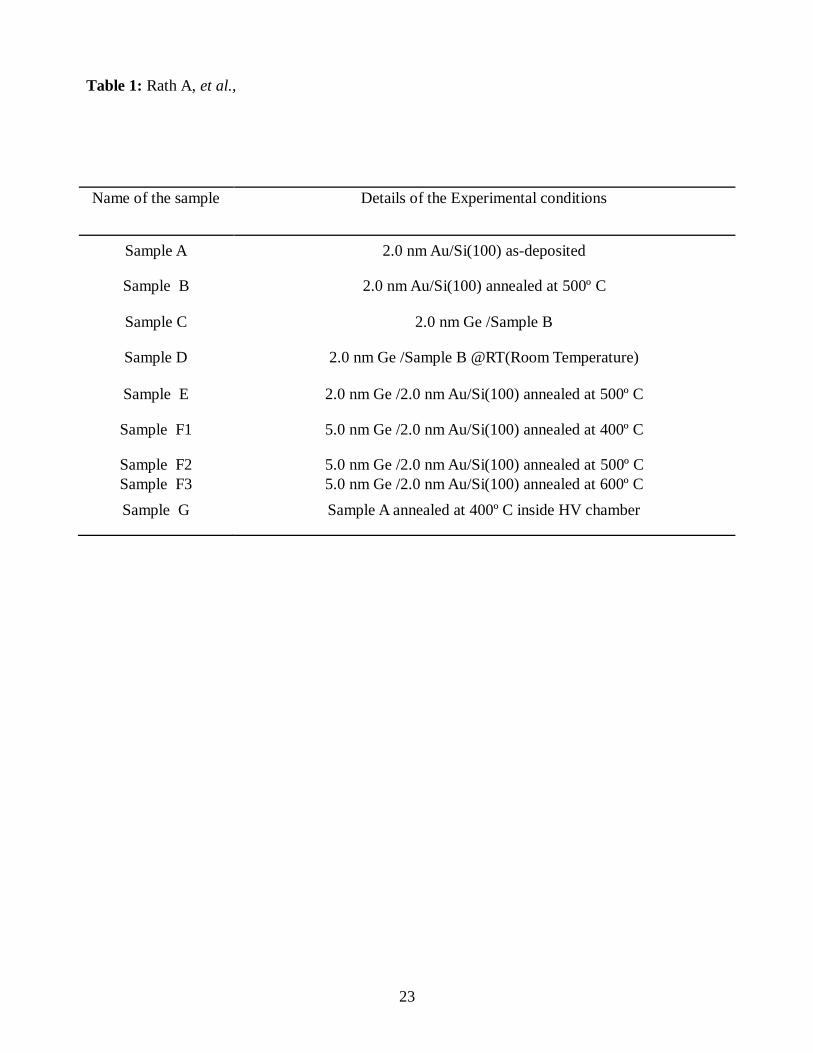
For this present study, we have prepared seven types of samples. For the first case (sample A),
a thin Au film of thickness of about 2.0 nm on n-type Si(100) of resistivity 10–20 cm, by MBE
method under ultra high vacuum conditions [34]. Si (100) substrates were loaded into the MBE
chamber and degassed at 600°C for about 12 hours inside the chamber and followed by flashing
for about 2 minutes by direct heating at a temperature of 1200°C. In this process, native oxide was
removed and a clean Si (100) surface was obtained. In-situ reflection high energy electron
diffraction (RHEED) measurements confirmed that the Si(100) surface is 2×1 reconstructed (data
not shown). On such ultra clean surfaces, 2.0 nm thick gold films were grown epitaxially by
evaporating Au from a Knudsen cell. Deposition rate was kept constant at 0.14 nm min-1
. Table 1
gives an overall view about the specimen used in this work. Thermal annealing of the as-deposited
sample (sample A) was carried out inside the UHV chamber at temperature of 500°C with a ramp
rate of 7°C min
-1(sample B). For the third case (sample C), we deposited a 2.0 nm gold on Si(100)
sample in the MBE chamber as explained above (like sample A) and about 2.0 nm Ge was further
deposited at a typical deposition rate of 0.6 ML/min (where one ML corresponds to 6.78 × 10¹⁴

5
atoms cm–2
for a Si(100) surface) at a substrate temperature of 500°C. For fourth case (sample D),
we have deposited 2.0 nm Ge on the Au patterned (after cooling the sample B to RT) surface while
the substrate is at room temperature (RT). For fifth case, 2.0 nm Au was first deposited followed by
2.0 nm Ge, while the substrate was kept at RT. After the deposition of Au and Ge at RT, the
specimen was annealed for 30 minutes at 500º C (sample E). For sixth case (sample F1, F2, F3), a
5.0 nm thick Ge film was deposited (instead of 2.0 nm) using same procedure as above on 2.0 nm
Au deposited surface( like sample A) with various substrate temperatures: 400°C (F1), 500
°C (F2)
and 600°C(F3). During the growth, chamber vacuum was 6.2 10
-10 mbar. The post-growth
characterization of the above samples were done with the field emission gun based scanning
electron microscopy (FEGSEM) measurements with 20 kV electrons using a Neon 40 cross-beam
system (M/S Carl Zeiss GmbH). Both cross-sectional and planar TEM specimens were prepared
from the above samples in which electron transparency was achieved through low energy Ar+ ion
milling. For seventh case (sample G), As-deposited MBE grown 2.0 nm Au /Si(100) (like sample
A) was in-situ annealed (up to 400°C) inside the TEM using single tilt heating holder (GATAN
628UHR, that has a tantalum furnace and can heat the specimen up to 1000°C) with the ramp rate of
7°C min
-1 . The temperature is measured by a Pt/Pt-Rh thermocouple and is accurate within a
couple of degrees. The holder has a water cooling system to avoid over heating of the sample
surroundings and the specimen chamber, while keeping only the sample at a specified temperature.
The summary of all the above samples are presented in Table 1. TEM measurements were
performed with 200 keV electrons (2010, JEOL HRTEM) and scanning TEM (STEM), high
resolution TEM measurements were done using 300 keV electrons in the Cs-corrected FEI Titan
80/300 system. The Rutherford backscattering (RBS) measurements were carried out using 2.0
MeV He+ ions.

6
3. Results and discussions
Figure 1(a) depicts a bright field TEM micrograph of as deposited 2.0 nm Au Film on
Si(100) without native oxide at the interface (sample A). Irregular and isolated gold nanostructures
of typical size/length of 29.3 ± 1.4 nm were formed. It should be noted that the error bars shown
here is the error in determining the peak value not the distribution variation. The selected area
diffraction pattern (SAD) taken on a group of nanostructures confirms the polycrystalline nature of
the gold films (figure 1(b)). A high resolution (HR) TEM taken on a single isolated nanostructure
shows the lattice spacing corresponding to elemental gold (inset figure 1(a)). The as-deposited
sample was annealed in-situ inside the UHV chamber at 500°C for 30 minutes (sample B).
Following this annealing in UHV, ex-situ TEM measurements (at room temperature) showed
rectangles/squares nanostructures aligned along set of planes {110} direction with respect to the
silicon substrate (Figure 1 (c)). This shape transformation is attributed to the strain relief mechanism
[20]. Inset of figure 1 (c) depicts the bright field HRTEM image of one of the nano island. Figure
1(d) and 1(e) shows the corresponding selected area diffraction (SAD) pattern taken on group of
rectangles/squares and cross-sectional HRTEM image of single rectangles, respectively. SAD
shows the single crystalline silicon background and some weak polycrystalline rings of gold along
with the dotted ring which corresponds to a d-spacing of about 0.226 nm which matches with the
several phases such as Au5Si2, Au5Si, Au7Si [35]. Figure 1(f) shows the SAD pattern taken at RT
from the same sample but heated upto 400°C (sample G). There was no signal of silicide formation
at 400°C. It should be noted that this annealing was carried out using in-situ TEM heating stage.
More discussion on the effect substrate temperature which plays an important role in formation of
gold-silicide nano alloy structures and helps to form Au-Ge bi-lobed structures will be discussed
later sections in this paper.

7
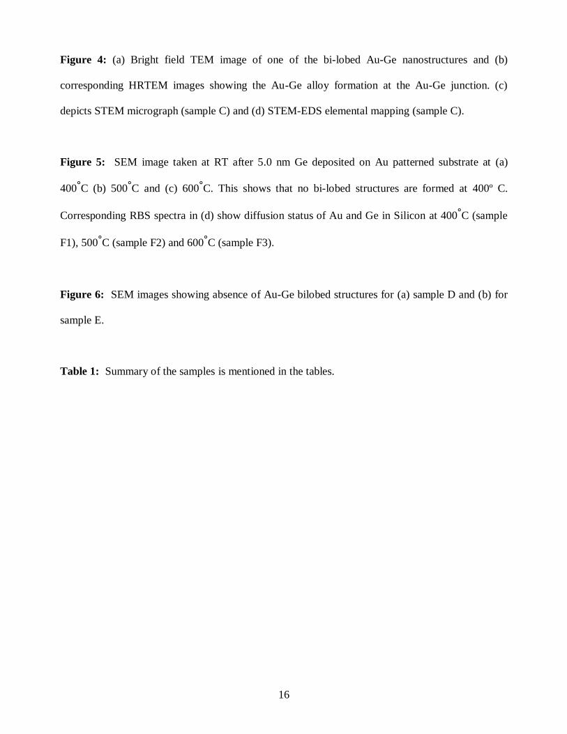
The average ratio of length along <1 1 0> to length along < 1 -1 0> direction, known as
“aspect ratio” was determined using several frames like figure 1(c). The length distribution along
<1 1 0> shows the Gaussian distribution and the average length is 48.1± 1.1 nm (figure 2(a)). The
average aspect ratio has been estimated by fitting the histograms with Gaussian distribution and the
average value is 0.998 ± 0.001 indicating that the islands are predominately compact in shape
(figure 2(b)). In our earlier work [20], we had shown that above 510°C, the average length (25.1 ±
1.6) and aspect ratio (1.12 ± 0.01) values were saturated during the in-situ thermal annealing inside
the TEM (high vacuum chamber). The percentage of particles having rectangular/square shape was
80%. But here (in UHV annealing), one can clearly see that the almost all the particles are become
squares/rectangles having decreased average aspect ratio and increased average length. When a ≈ 2
nm Ge was further deposited (sample C) using MBE system on the above rectangular/square
patterned surface at substrate temperature 500°C inside the UHV chamber, bilobed nanostructures
of Au and Ge were formed. It should be noted that AuSi nanalloys are used as seeding positions for
Au-Ge lobe-lobe structures. This means that, Au deposition and annealing and Ge deposition after
Au deposition are done in sequentially without any break in the vacuum. In figure 3(a), SEM image
shows the bi-lobed nanostructures of Au and Ge, where the bright contrast is the gold and other one
is for the Ge. As Au is higher Z material, more secondary electrons are emitted from the Au region
than from Ge region and this causes the contrast difference between gold and germanium in SEM
images. The average length and aspect ratio of the bi-lobed (including both Au and Ge) structures is
116 ± 1.8 nm and 1.12 ± 0.03 respectively. The length distribution is fitted with Gaussian
distribution and the aspect ratio is fitted with log normal distribution to estimate the average value
(figure 2(c)-(d)). In addition to the bi-lobed structures, one can see the formation of rectangular
shaped Ge nanostructures having typical size ~ 3.0 nm (figure 3(a)). In figure 3(c), SEM images
taken at 54° tilt have been shown. This shows a three dimensional nature of the Au-Ge

8
nanostructures. Figure 3(b) and 3(d) depicts high resolution XTEM of the epitaxially grown Ge
nano structures and Au-Ge bilobed structures on the silicon substrate respectively. It shows the
diffusion of gold into the silicon substrate, where as there was not appreciable diffusion of Ge. This
is further confirmed with Rutherford backscattering spectrometry (RBS) method. The RBS results
would be discussed in the following sub-section.
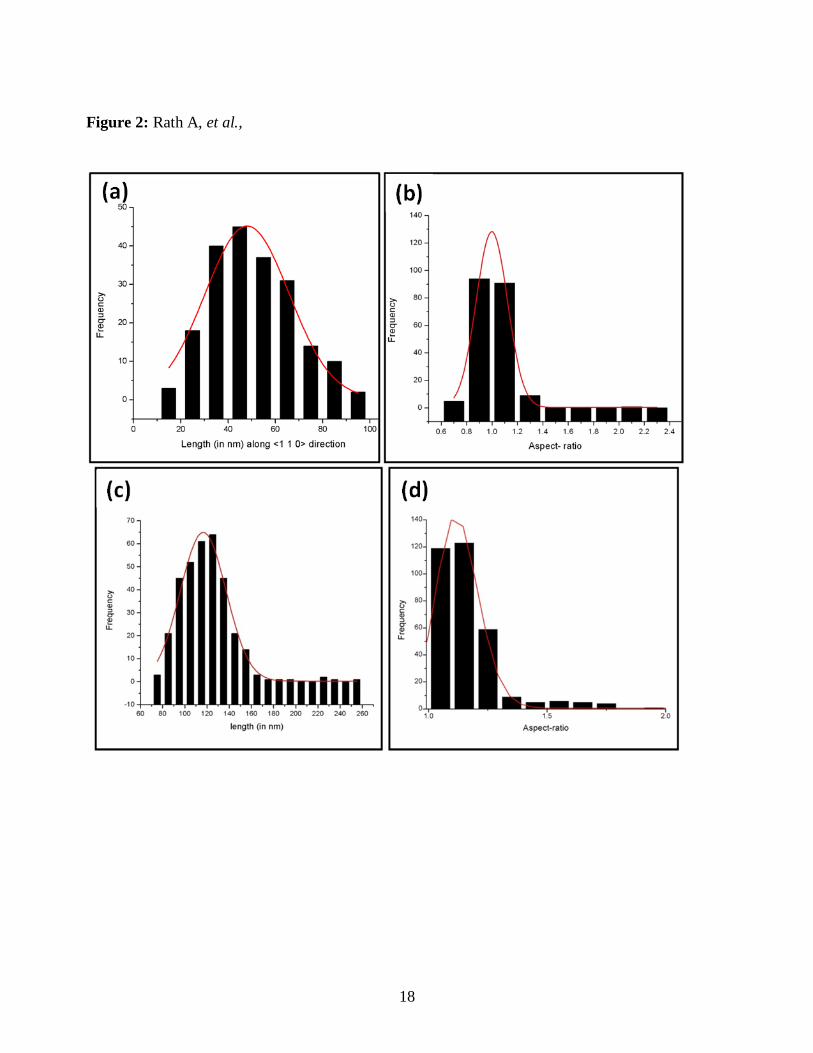
We now discuss on the detail structure of bi-lobed structures and the interface between the
Au lobe and Ge lobe. The bright field (BF) TEM image in figure 4(a) depicted one of the bilobed
structures and the corresponding HRTEM image is shown in figure 4(b). At the Au–Ge junction
(dotted circle) using high resolution images, the d-spacing has been found to be of about 0.332 nm
and 0.279 nm. These lattice spacing do not match with the Au, Ge or Si but matches quite well with
the (224) and (324) plane of tetragonal phase of Au0.6Ge0.4 [36]. According to bulk Au-Ge phase
diagram, the above composition is formed at 520°C which is comparable with our growth
temperature. Also, the lattice spacing value of 0.279 is close to (200) planes of Si0.25Ge0.75. We
need to carry our more studies to come to a conclusion on the interfacial structure (i.e. whether it is
AuGe or SiGe). It should be noted that deviations in the nano-scale phase-diagram to bulk phase
diagram are reported by Sutter et al. [27].
Figure 4 (c), depicts a STEM– HAADF image showing the large area of the specimen with
bi-lobed structures. This shows the expected Z-contrast, so that Au appears brighter than the Ge
over layer and Si substrate. To analyze the local distribution of Au in these structures, STEM–x-ray
energy dispersive spectrometry (XEDS) elemental mapping was carried out. In Figure 4(d), STEM
EDS elemental mapping shows the presence of Au and Ge in a single bi-lobed structure. Though it
is clear about the phase separation of gold (from 4(d) – Au M signal), but it is not very clear about
the possible presence of SiGe. We need to carryout high resolution cross-section STEM
measurements to obtain this information.
9
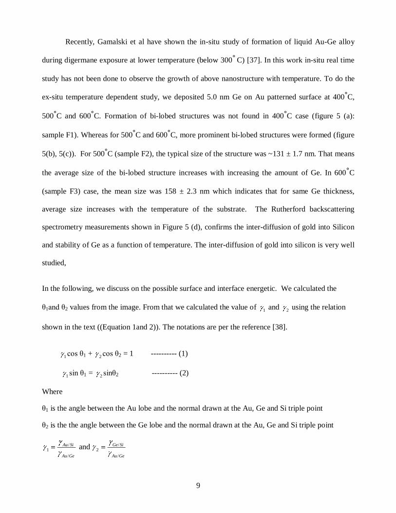
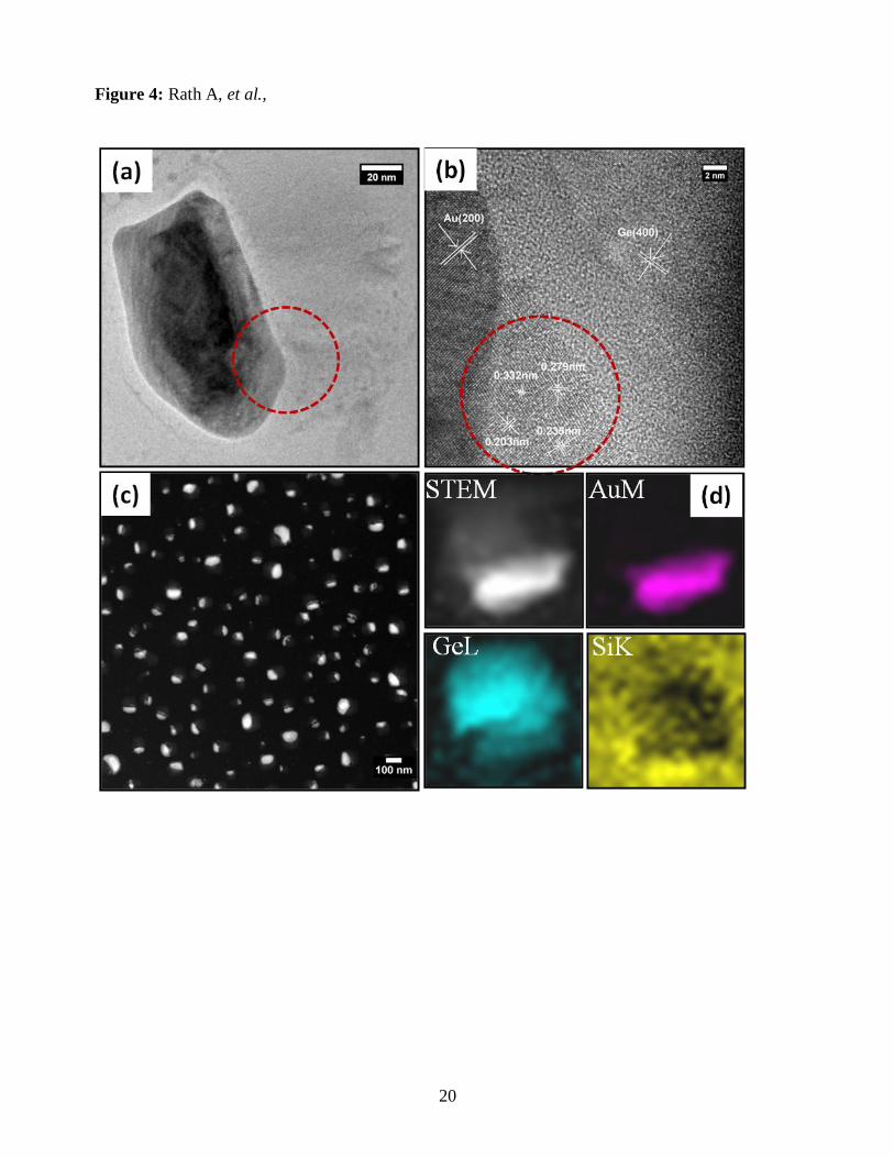
Recently, Gamalski et al have shown the in-situ study of formation of liquid Au-Ge alloy
during digermane exposure at lower temperature (below 300°
C) [37]. In this work in-situ real time
study has not been done to observe the growth of above nanostructure with temperature. To do the
ex-situ temperature dependent study, we deposited 5.0 nm Ge on Au patterned surface at 400°C,
500°C and 600
°C. Formation of bi-lobed structures was not found in 400
°C case (figure 5 (a):
sample F1). Whereas for 500°C and 600
°C, more prominent bi-lobed structures were formed (figure
5(b), 5(c)). For 500°C (sample F2), the typical size of the structure was ~131 ± 1.7 nm. That means
the average size of the bi-lobed structure increases with increasing the amount of Ge. In 600°C
(sample F3) case, the mean size was 158 ± 2.3 nm which indicates that for same Ge thickness,
average size increases with the temperature of the substrate. The Rutherford backscattering
spectrometry measurements shown in Figure 5 (d), confirms the inter-diffusion of gold into Silicon
and stability of Ge as a function of temperature. The inter-diffusion of gold into silicon is very well
studied,
In the following, we discuss on the possible surface and interface energetic. We calculated the
θ1and θ2 values from the image. From that we calculated the value of 1 and
2 using the relation
shown in the text ((Equation 1and 2)). The notations are per the reference [38].
1cos θ1 +
2cos θ2 = 1 ---------- (1)
1sin θ1 =
2sinθ2 ---------- (2)
Where
θ1 is the angle between the Au lobe and the normal drawn at the Au, Ge and Si triple point
θ2 is the the angle between the Ge lobe and the normal drawn at the Au, Ge and Si triple point
/ /1 2
/ /
and Au Si Ge Si
Au Ge Au Ge

10
(Where/Au Si
,/Ge Si
and/Au Ge
are the interfacial free energies for the Au-Si, Ge-Si and Au-Ge
interfaces).
To check whether the bi-lobed structures are equilibrium structures or not, we calculated the
1 and
2values for the bi-lobed structures and applied the formulas used by the Yuan et al [38] in
their calculation. The value of the 1 (= 1.05) and
2 (= 1.07) were well matched with the studied
done by Yuan et al [38]. So these Au-Ge bilobed structures are most likely the equilibrium
structures. We have found that by changing the Ge thickness and working temperature, the size of
these bilobed structures can be tuned. From the all above studies, it was found that the heated Au-Si
alloy structures may play a major role in formation of such bilobed structures. During the deposition
of Ge, gold silicide particles act as nucleation center for the growth of Ge. The minimum surface
and interfacial energy for the system is achieved when the Ge is nested within Au and this would be
a critical factor during the nucleation of the Ge crystals, where surface energy considerations
determine the size and shape of the critical nucleus. As the deposition continues, the smaller liquid
droplets provide a rapid diffusion path for the incoming Ge atoms, which find it energetically
favorable to join already-nucleated crystals rather than to nucleate new ones. For larger thickness of
Ge (5.0 nm), more Ge is nested within Au due to the enhancement of material availability. It
resulted in increase in size of the Au-Ge bilobed structures. One can clearly see that at constant
temperature of 500°C, the size of the Au-Ge bilobed structures was typically~ 116nm for 2nm Ge
case whereas for 5nm Ge case it was ~131 nm.
To study the effect of substrate temperature, we deposited 2.0 nm Ge on the gold patterned
substrate at room temperature (sample D). In figure 6(a), SEM image shows the formation of
rectangular gold structures and Ge over layers in between the gold structures. Formation of bi-lobed
structures was not found in this case. Also we deposited 2 nm gold and then 2 nm Ge on Si(100)
substrate and heated it upto 500°C (sample E). During annealing, one would expect the formation of

11
the regular structure following the substrate symmetry of Si(100) as seen in our previous work [20].
But here, both Au and Ge were present on the surface during annealing and as the thermal diffusion
coefficient of both the materials is different [39], we observed the formation of irregular Au-Ge
structures (figure 6(b)). Also, it has been reported that the AuxGe1-x (0.27<x<0.6) shows super
conductivity with a transition temperature up to ~ 2K [40]. There is a possibility to use the
combination of Au, AuxSi1-x, Ge, and AuxGe 1-x, structures. But, more studies are necessary to have
a control on specific combination of the above structures so that technological applications become
viable.
4. Conclusions
We have reported the formation of Au-Ge bilobed nanostructures by using molecular beam
epitaxy. The effect of substrate temperature, material deposition sequence and also the role of gold
silicide on the formation bi-lobed structures were studied in detail.
Acknowledgements
P. V. Satyam would like to thank the Department of Atomic Energy, Government of India,
for 11th Plan Project No 11-R&D-IOP-5.09-0100 and the University of Bremen, Germany, for his
sabbatical visiting program.

12
References:
[1] Freund H J 2002 Surf. Sci. 500 271
[2] Boettcher S W, Strandwitz N C, Schierhorn M, Lock N, Lonergan M C, and Stucky G D,
2007 Nat. Mater. 6 592
[3] Berbezier I, Ronda A, Portavoce A and Motta N 2003 Appl. Phys. Lett. 83 4833
[4] Eaglesham D J, Unterwald F C and Jacobson D C 1993 Phys. Rev. Lett. 70 966
[5] Fan H J, Werner P, and Zacharias M 2006 Small 2 700 and references therein.
[6] Li Y B, Bando Y and Golberg D 2004 Adv. Mater. 16 37.
[7] Goldberger, He J, Zhang R R, Lee Y F, Yan S W, Choi H Q and Yang H J 2003
Nature, 422 599
[8] Green A K and Bauer E 1981 Surf. Sci. 103 L127
[9] Meinel K and Katzer D 1992 Appl. Surf. Sci. 514 56
[10] Hiraki A and Iwami M 1974 Jpn. J. Appl. Phys. Suppl. 2 749
[11] Han J, Jeon D, and Kuk Y 1997 Surf. Sci. 376 237
[12] Baumann F H and Schroter W 1991 Phys. Rev. B 43 6510
[13] Bokhonov B and Korchagin M 2000 J. Alloys Compd. 312 238
[14] Le Lay G 1983 Sur.Sci. 132 169
[15] Bhatta U M, Dash J K, Roy A, Rath A, Satyam P V 2009 J. Phys. Condens. Matter 21
205403; Bhatta U M, Dash J K, Rath A, Satyam P V 2009 Applied Surface Science 256 567
[16] Brongersma S H et al. 1998 Phys. Rev. Letts. 80 3795–3798
[17] Mundschau M, Bauer E, Telieps W 1989 Surface science 213 381-392
[18] Kopatzki E, Giinther S, Nichtl-Peche W and Behm R J 1993 Surface Science 284 154-166
[19] Frank S, Wedler H, and Behm R J 2002 Phys Rev. B 66 155435
[20] Rath A, Dash J K, Juluri R R, Rosenauer A and Satyam P V 2011 J. Phys D: Appl Phys.

13
44 115301
[21] Hsieh Y F, Chen L J, Marshall E D and Lau S S 1987 Appl. Phys. Lett. 51 1588
[22]Thomas O, Delage S, d’Heurle F M and Scilla G 1989 Appl. Phys. Lett. 54 228
[23] Hong S Q, Comrie C M, Russell S W and Mayer J W 1991 Appl. Phys. 70 3655
[24] Rosenberg J J 1983 IEEE Trans. Electron. Devices ED-30 1602
[25] Adhikari H, Marshall A F, Goldthorpe I A, Chidsey C E D and McIntyre P C 2007 ACS
Nano 1 415
[26] Kohler R, Neumann W, Schmidbauer M, Hanke M, Grigoriev D, Schäfer P, Kirmse H,
Häusler I, and Schneider R, NanoScience and Technology,Semiconductor Nanostructures ( D.
Bimberg (ed.) chapter 5) Springer, 2008, 97-121, DOI: 10.1007/978-3-540-77899-8_5
[27] Sutter E A and Sutter P W 2010 ACS Nano 4 4943–7
[28] Neumann W, Kirmse H, Häusler I, Otto I and Hähnert I 2004 J. Alloys and
Compounds 382 2
[29] Goldfarb I, 2005 Phys. Rev.Lett. 95 025501
[30] Kim B, Tersoff J, Kodambaka S, Reuter M C and Ross F M 2008 Science 322 1070
[31] Gaudet S, Detavernier C, Kellock A J, Desjardins P and Lavoie C 2006 J. Vac. Sci. Technol. A
24(3) 474.
[32] Sutter E and Sutter P 2011 Nanotechnology 22 295605
[33] Chueh Y L et al 2010 Nano Lett. 10 393
[34] Goswami D K, Satpati B, Satyam P V and Dev B N 2003 Curr. Sci. 84 903
[35] Au7Si (JCPDS 26-0723), Au5Si (JCPDS 26-0725), Au5Si2 (JCPDS 36-0938)
[36] JCPDS 18-0551
[37] Gamalski A D, Tersoff J, Sharma R, Ducati C and Hofmann S 2010 Nano Lett. 10 2972
[38] Yuan C W, Shin S J, Liao C Y, Guzman J, Stone P R, Watanabe M, Ager III J W, Haller E E
and Chrzan D C 2008 Appl.Phys.Lett. 93 193114.

14
[39] Srivastava D and Garrison B J 1992 Phys. Rev. B 46 1472
[40] Luo H L, Hamilton D C and Merriam M F 1964 Science 145 581
15
Figure captions:
Figure 1: (a) As-deposited (sample A) showing gold nanostructures with corresponding high
resolution image of one of the islands which is showing the d-spacing of Au(111) in the inset (b)
SAD pattern showing reflection of both Si and Au, (c) bright field TEM image taken for the sample
that was annealed at 500°C in UHV chamber (sample B) with corresponding high resolution image
of one of the single islands (inset), (d) SAD pattern showing the formation gold silicide along with
the reflection Au and Si for the sample B, (e) bright field high resolution XTEM image of one of
the nanostructure (sample B) showing inter-diffusion of Au into Si. (f) Depicts a SAD pattern taken
at RT for the sample that was annealed in-situ TEM at 400°C(sample G) and then cooled to RT.
This shows no gold silicide formation at 400°C.
Figure 2: (a) Length distribution(fitted with Gaussian distribution) along <1 1 0> direction, of the
sample shown in Fig 1 (c) which shows an average length of 48.1± 1.1 nm and (b)corresponding
aspect ratio distribution and average aspect ratio is 0.99 ± 0.01 ( here the histograms are fitted with
Gaussian distribution to estimate the mean aspect ratio) (c) length distribution(fitted with Gaussian
distribution) of the sample shown in Fig 3(a) (for several frames) which shows the average length
is 116 ± 1.8 nm and (d) corresponding aspect ratio distribution and average aspect ratio is 1.12 ±
0.03 ( here the histograms are fitted with log -normal distribution to estimate the mean aspect ratio).
Figure 3: (a) SEM image taken at 0º tilt (c) 54º tilt; (b) depicts a XTEM image of epitaxially grown
Ge nano structures and (d) for Au-Ge bilobed structures (sample C).
16
Figure 4: (a) Bright field TEM image of one of the bi-lobed Au-Ge nanostructures and (b)
corresponding HRTEM images showing the Au-Ge alloy formation at the Au-Ge junction. (c)
depicts STEM micrograph (sample C) and (d) STEM-EDS elemental mapping (sample C).
Figure 5: SEM image taken at RT after 5.0 nm Ge deposited on Au patterned substrate at (a)
400°C (b) 500
°C and (c) 600
°C. This shows that no bi-lobed structures are formed at 400º C.
Corresponding RBS spectra in (d) show diffusion status of Au and Ge in Silicon at 400°C (sample
F1), 500°C (sample F2) and 600
°C (sample F3).
Figure 6: SEM images showing absence of Au-Ge bilobed structures for (a) sample D and (b) for
sample E.
Table 1: Summary of the samples is mentioned in the tables.

17
Figure 1: Rath A, et al.,
18
Figure 2: Rath A, et al.,

19
Figure 3: Rath A, et al.,
20
Figure 4: Rath A, et al.,
21
Figure 5: Rath A, et al.,

22
Figure 6: Rath A, et al.,
23
Table 1: Rath A, et al.,
Name of the sample Details of the Experimental conditions
Sample A 2.0 nm Au/Si(100) as-deposited
Sample B 2.0 nm Au/Si(100) annealed at 500º C
Sample C 2.0 nm Ge /Sample B
Sample D 2.0 nm Ge /Sample B @RT(Room Temperature)
Sample E 2.0 nm Ge /2.0 nm Au/Si(100) annealed at 500º C
Sample F1 5.0 nm Ge /2.0 nm Au/Si(100) annealed at 400º C
Sample F2 5.0 nm Ge /2.0 nm Au/Si(100) annealed at 500º C Sample F3 5.0 nm Ge /2.0 nm Au/Si(100) annealed at 600º C Sample G Sample A annealed at 400º C inside HV chamber