NANO-OPTOMECHANICAL STATIC RANDOM ACCESS MEMORY …nocweba.ntu.edu.sg/laq_mems/conference/IEEE...
4
NANO-OPTOMECHANICAL STATIC RANDOM ACCESS MEMORY (SRAM) B. Dong 1, 2 , H. Cai 2 , Y. D. Gu 2 , Z. C. Yang 3 , Y. F. Jin 3 , Y. L. Hao 3 , D. L. Kwong 2 and A. Q. Liu 1† 1 School of Electrical & Electronic Engineering, Nanyang Technological University, Singapore 639798 2 Institute of Microelectronics, A*STAR (Agency for Science, Technology and Research) Singapore 117685 3 National Key Laboratory of Science and Technology on Micro/Nano Fabrication Institute of Microelectronics, Peking University, Beijing 100871, China ABSTRACT This paper reports an on chip nano-optomechanical SRAM, which is integrated with light modulation system on a single silicon chip. In particular, a doubly-clamped silicon beam shows bistability due to the non-linear optical gradient force generated from a ring resonator. The memory states are assigned with two stable deformation positions, which can be switched by modulating the control light’s power with the integrated optical modulator. The optical SRAM has write/read time around 120 ns, which is much faster as compared with traditional MEMS memory. Meanwhile, the write and read processes can happen concurrently without interference, which further reduces the time as compared with conventional electrical enabled SRAM. INTRODUCTION The exploration of information in modern society challenge the way we store and process information. There is always a strong demand for high speed, energy efficient and compact approaches to store signals in the current high speed and high capacity data processing system. Various approaches have been investigated such as magnetic storage, opto-electro based photonic memory and mechanical memory [1, 2]. MEMS/NEMS memory has been developed for more than 20 years. Most of the memories are based on either mechanical bistability [3] or material based bistability [4]. However, MEMS memory has drawbacks such as large scale and low speed. NEMS memory based on optomechanical effects shows great potential in optical storage on silicon photonic circuits due to its high speed, small size and good integrability [5-7]. This paper reports an on chip nano-optomechanical SRAM, which is integrated with light modulation system on a single silicon chip. The memory states are stored as deformation of doubly-clamped silicon beam, while the silicon beam shows bistability which is induced by the nonlinear optical gradient force. The optical SRAM can be utilized in all optical computing, with high speed (120 ns) and low power consumption. The CMOS compatible fabrication processes also make the optical SRAM cheap and can be easily integrated with other systems. DESIGN AND THEORY The schematic of the nano-optomechanical SRAM is shown in Fig. 1(a). Both “WRITE” and “READ” light from demultiplexer are coupled into the on-chip memory array. The “WRITE” light go through the integrated intensity modulator before entering the memory array. The intensity (a) (b) (c) Figure 1: (a) Schematic of the nano-optomechanical memory, (b) layout of the optical memory and (c) spectrum illustration of the optical memory. 978-1-4799-7955-4/15/$31.00 ©2015 IEEE 49 MEMS 2015, Estoril, PORTUGAL, 18 - 22 January, 2015
-
Upload
hoangduong -
Category
Documents
-
view
219 -
download
0
Transcript of NANO-OPTOMECHANICAL STATIC RANDOM ACCESS MEMORY …nocweba.ntu.edu.sg/laq_mems/conference/IEEE...

NANO-OPTOMECHANICAL STATIC RANDOM ACCESS MEMORY (SRAM) B. Dong1, 2, H. Cai2, Y. D. Gu2, Z. C. Yang3, Y. F. Jin3, Y. L. Hao3, D. L. Kwong2 and A. Q. Liu1†
1School of Electrical & Electronic Engineering, Nanyang Technological University, Singapore 639798 2Institute of Microelectronics, A*STAR (Agency for Science, Technology and Research)
Singapore 117685 3National Key Laboratory of Science and Technology on Micro/Nano Fabrication
Institute of Microelectronics, Peking University, Beijing 100871, China
ABSTRACT This paper reports an on chip nano-optomechanical
SRAM, which is integrated with light modulation system on a single silicon chip. In particular, a doubly-clamped silicon beam shows bistability due to the non-linear optical gradient force generated from a ring resonator. The memory states are assigned with two stable deformation positions, which can be switched by modulating the control light’s power with the integrated optical modulator. The optical SRAM has write/read time around 120 ns, which is much faster as compared with traditional MEMS memory. Meanwhile, the write and read processes can happen concurrently without interference, which further reduces the time as compared with conventional electrical enabled SRAM.
INTRODUCTION The exploration of information in modern society
challenge the way we store and process information. There is always a strong demand for high speed, energy efficient and compact approaches to store signals in the current high speed and high capacity data processing system. Various approaches have been investigated such as magnetic storage, opto-electro based photonic memory and mechanical memory [1, 2]. MEMS/NEMS memory has been developed for more than 20 years. Most of the memories are based on either mechanical bistability [3] or material based bistability [4]. However, MEMS memory has drawbacks such as large scale and low speed. NEMS memory based on optomechanical effects shows great potential in optical storage on silicon photonic circuits due to its high speed, small size and good integrability [5-7].
This paper reports an on chip nano-optomechanical SRAM, which is integrated with light modulation system on a single silicon chip. The memory states are stored as deformation of doubly-clamped silicon beam, while the silicon beam shows bistability which is induced by the nonlinear optical gradient force. The optical SRAM can be utilized in all optical computing, with high speed (120 ns) and low power consumption. The CMOS compatible fabrication processes also make the optical SRAM cheap and can be easily integrated with other systems.
DESIGN AND THEORY
The schematic of the nano-optomechanical SRAM is shown in Fig. 1(a). Both “WRITE” and “READ” light from demultiplexer are coupled into the on-chip memory array. The “WRITE” light go through the integrated intensity modulator before entering the memory array. The intensity
(a)
(b)
(c)
Figure 1: (a) Schematic of the nano-optomechanical memory, (b) layout of the optical memory and (c) spectrum illustration of the optical memory.
978-1-4799-7955-4/15/$31.00 ©2015 IEEE 49 MEMS 2015, Estoril, PORTUGAL, 18 - 22 January, 2015

of “WRITE” light is modulated by the address controlled intensity modulator such that the intensity is increased when writing “1” and decrease when writing “0. Each wavelength can only interact with a single memory cell such that the deformation of a particular unit cell is modulated. Meanwhile, the “READ” light interacts with a single memory cell for memory states read out. (Fig 1(b)). The “WRITE” light and “READ” light are located in different spectra region to avoid interference. Fig. 1(c) shows the operation of the optical memory. By pumping in a pulsed high power (P1) write light, the memory can be switched to state “1” while the transmission of read light is at high power level (PH). The memory is switched to state “0” by further reducing the write light power to P0. As a result, the transmission of the read light is low (PL). Due to the bistability of the memory, the memory can maintain its state with a moderate power level (Pm) to save power consumption.
The schematic of the unit cell of the SRAM array is shown in Fig. (2). The unit cell consists of a bus waveguide, a ring resonator and a doubly-clamped silicon beam. Optical gradient force is generated by control light in the ring resonator over the side coupled silicon beam via evanescent wave. The ring resonator is 40 µm in diameter and 450 nm in width. The silicon beam is 200 nm in width and the coupling gap in-between is 200 nm.
Figure 2: Schematic of nano-optomechanical memory unit cell
The operation of memory requires two lights to realize write and read processes. A red-detuned write light is coupled from the bus waveguide into the ring resonator. Thereafter, the optical gradient force is conducted between the ring resonator and the silicon beam, which pulls the silicon beam towards the ring resonator. The signal light, known as read light, is also coupled into the ring resonator and sensed at the output port. The wavelength of the read light overlaps with the resonance wavelength of the ring resonator. When the power of the write light is increased, the optical gradient force is increased and the mechanical arc moves towards the ring resonator along x direction. The displacement Δx of the silicon beam results in the change in the effective refractive index Δneff of the ring resonator, causing a red shift of the ring resonance wavelength Δλr. The read light can be transmitted through the waveguide since its wavelength is no longer overlapped with the
resonance wavelength now. The displacement of the silicon beam can affect the transmission of the read light by altering the resonance wavelength of the ring resonator. Therefore, by pumping a red-detuned write light with different power level, the transmission of the read light can be controlled and the statuses of the doubly-clamped silicon beam, which is known as the on-state and the off-sate of the switch, can be switched.
The deformation of the doubly-clamped silicon beam is determined by two forces: optical gradient force and mechanical spring force. The mechanical spring force, increases linearly as the deformation of the silicon beam increases. The generated optical force by the single wavelength laser Wλ can be expressed as
2 2
2 ( )( )
( ) ( )e optical om
opticaleff
P g xF x
n x xγ
γ= −
Δ + (1)
where eγ is the external damping due to waveguide-ring
coupling, opticalP is the light power, effn is the effective
refractive index, omg is the optomechanical coupling
coefficient, is the total damping coefficient and (x) is the laser detuning which is defined as
1 1( ) 2 ( )( ) W
x cx
πλ λ
Δ = − (2)
where (x) is the resonance wavelength of the ring resonator, which is related to the effective refractive index and therefore the deformation of the doubly-clamped silicon beam. The write light’s wavelength detuning is therefore defined as
( )0Wδ λ λ= − (3)
where ( )0λ is the resonance wavelength of the ring
resonator at zero deformation.
Figure 3: Bi-stability of the unit cell of SRAM at various laser detuning.
50

The doubly-clamped silicon deforms in different paths at different wavelength detuning as shown in Fig. 3. When the wavelength detuning is 0.1 nm, the doubly-clamped silicon beam shows only one stable position at all time. Therefore, the doubly-clamped silicon beam shows no bistability. When the wavelength detuning is increased to 0.125 nm, there is only a very narrow region that the doubly-clamped silicon beam shows two stable positions, and the transition curve is close to a vertical line. This is the critical condition where the doubly-clamped silicon beam starts to show bistability. When the wavelength detuning is increased to 0.175 nm, the bistable region is further broadened. Therefore, besides the write light power, the wavelength is critical to control the bistability of the doubly-clamped beam.
The doubly-clamped silicon beam shows bistability when it is deformed by the optical gradient force. But such bistability is not due to the mechanical properties of the doubly-clamped silicon beam, but the non-linear properties of the optical gradient force. The bistability of the doubly-clamped silicon beam can therefore be manipulated by controlling the light wavelength and power, providing more freedom in the operation of the optomechanical memory.
FABRICATION Figure 4 shows the scanning electron microscope
(SEM) images of fabricated nano-optomechanical SRAM with CMOS compatible nano-silicon-photonics technology.
(a)
(b)
Figure 4: SEM images of the optical memory.
The waveguide structures have a width of 450 nm and a
height of 220 nm. The doubly-clamped silicon beam is designed to be 200 nm in width while the coupling gap between the ring resonator and the silicon beam is 200 nm. The waveguides and ring resonators are patterned by a two-step deep UV lithography and RIE process. The rib structure has a 70-nm silicon slab layer to support the ring resonator. After etching, a 2-µm SiO2 layer is deposited on the structure layers. A 40-nm Al2O3 is deposited and patterned, which is used as the protection film to protect the • xed structures and leave the window area opened for suspended structures. Finally, HF vapor selectively undercuts the buried oxide layer in the window area to release the movable structures.
EXPERIMENTS AND DISCUSSIONS The intensity is experimentally tested by applying
voltage across the p-i-n junction. Initially, the resonance wavelength of the ring resonator is 1587.94, which is the wavelength of “WRITE” light. By applying the voltage of the p-i-n junction, the resonance wavelength is red shifted due to the injection of the electrons. As a result, the transmission power of the “WRITE” light in reduced by 3 dB at 2.25 V and 2dB at 1.75 V. By controlling the voltage across the p-i-n junction, the intensity of the “WRITE” light can therefore be modulated.
Figure 5: Tested transmission spectra of intensity modulator.
The power of the write light is modulated among P1, Pm
and P0. The transmission spectra of the optical memory at various power of the red detuned (0.36 nm) write light is shown in Fig. 6. Initially, the power level is Pm (-8 dBm, the black line), the resonance wavelength is close to 1593 nm, which is the wavelength of the read light, the transmission of the read light is low, and the memory is at “0” state. When the power level is increased to P1 (-6 dBm, the red line), the resonance wavelength shifts to 1591.6 nm, the transmission of the read light is high and the memory is at “1” state. After the power level is decreased to Pm again (the blue line), the resonance wavelength maintains its current position with negligible blue shift, and the memory remain at “1”. When the power is further reduced to P0 (-10 dBm, the pink line), the resonance wavelength reduces to
51
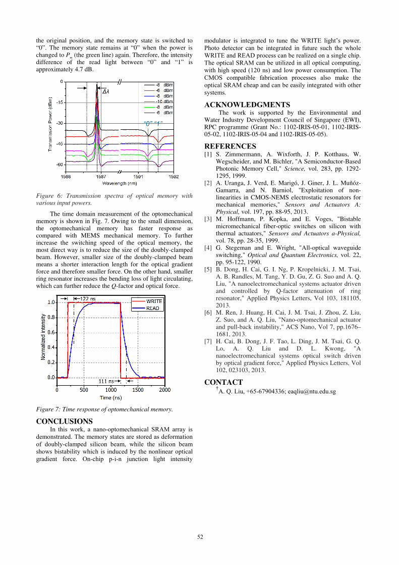
the original position, and the memory state is switched to “0”. The memory state remains at “0” when the power is changed to Pm (the green line) again. Therefore, the intensity difference of the read light between “0” and “1” is approximately 4.7 dB.
Figure 6: Transmission spectra of optical memory with various input powers.
The time domain measurement of the optomechanical memory is shown in Fig. 7. Owing to the small dimension, the optomechanical memory has faster response as compared with MEMS mechanical memory. To further increase the switching speed of the optical memory, the most direct way is to reduce the size of the doubly-clamped beam. However, smaller size of the doubly-clamped beam means a shorter interaction length for the optical gradient force and therefore smaller force. On the other hand, smaller ring resonator increases the bending loss of light circulating, which can further reduce the Q-factor and optical force.
Figure 7: Time response of optomechanical memory.
CONCLUSIONS In this work, a nano-optomechanical SRAM array is
demonstrated. The memory states are stored as deformation of doubly-clamped silicon beam, while the silicon beam shows bistability which is induced by the nonlinear optical gradient force. On-chip p-i-n junction light intensity
modulator is integrated to tune the WRITE light’s power. Photo detector can be integrated in future such the whole WRITE and READ process can be realized on a single chip. The optical SRAM can be utilized in all optical computing, with high speed (120 ns) and low power consumption. The CMOS compatible fabrication processes also make the optical SRAM cheap and can be easily integrated with other systems.
ACKNOWLEDGMENTS The work is supported by the Environmental and
Water Industry Development Council of Singapore (EWI), RPC programme (Grant No.: 1102-IRIS-05-01, 1102-IRIS-05-02, 1102-IRIS-05-04 and 1102-IRIS-05-05).
REFERENCES [1] S. Zimmermann, A. Wixforth, J. P. Kotthaus, W.
Wegscheider, and M. Bichler, "A Semiconductor-Based Photonic Memory Cell," Science, vol. 283, pp. 1292-1295, 1999.
[2] A. Uranga, J. Verd, E. Marigó, J. Giner, J. L. Muñóz-Gamarra, and N. Barniol, "Exploitation of non-linearities in CMOS-NEMS electrostatic resonators for mechanical memories," Sensors and Actuators A: Physical, vol. 197, pp. 88-95, 2013.
[3] M. Hoffmann, P. Kopka, and E. Voges, "Bistable micromechanical fiber-optic switches on silicon with thermal actuators," Sensors and Actuators a-Physical, vol. 78, pp. 28-35, 1999.
[4] G. Stegeman and E. Wright, "All-optical waveguide switching," Optical and Quantum Electronics, vol. 22, pp. 95-122, 1990.
[5] B. Dong, H. Cai, G. I. Ng, P. Kropelnicki, J. M. Tsai, A. B. Randles, M. Tang, Y. D. Gu, Z. G. Suo and A. Q. Liu, "A nanoelectromechanical systems actuator driven and controlled by Q-factor attenuation of ring resonator," Applied Physics Letters, Vol 103, 181105, 2013.
[6] M. Ren, J. Huang, H. Cai, J. M. Tsai, J. Zhou, Z. Liu, Z. Suo, and A. Q. Liu, "Nano-optomechanical actuator and pull-back instability," ACS Nano, Vol 7, pp.1676–1681, 2013.
[7] H. Cai, B. Dong, J. F. Tao, L. Ding, J. M. Tsai, G. Q. Lo, A. Q. Liu and D. L. Kwong, "A nanoelectromechanical systems optical switch driven by optical gradient force," Applied Physics Letters, Vol 102, 023103, 2013.
CONTACT †A. Q. Liu, +65-67904336; [email protected]
52