NANO LETTERS Nanoscale Electronic Inhomogeneity...
5
Nanoscale Electronic Inhomogeneity in In 2 Se 3 Nanoribbons Revealed by Microwave Impedance Microscopy Keji Lai, †,‡ Hailin Peng, †,§ Worasom Kundhikanjana, ‡ David T. Schoen, § Chong Xie, § Stefan Meister, § Yi Cui,* ,§ Michael A. Kelly, § and Zhi-Xun Shen* ,‡ Department of Applied Physics and Department of Materials Science and Engineering, Stanford UniVersity, Stanford, California 94305 Received January 21, 2009 ABSTRACT Driven by interactions due to the charge, spin, orbital, and lattice degrees of freedom, nanoscale inhomogeneity has emerged as a new theme for materials with novel properties near multiphase boundaries. As vividly demonstrated in complex metal oxides (see refs 1-5) and chalcogenides (see refs 6 and 7), these microscopic phases are of great scientific and technological importance for research in high-temperature superconductors (see refs 1 and 2), colossal magnetoresistance effect (see ref 4), phase-change memories (see refs 5 and 6), and domain switching opera- tions (see refs 7-9). Direct imaging on dielectric properties of these local phases, however, presents a big challenge for existing scanning probe techniques. Here, we report the observation of electronic inhomogeneity in indium selenide (In 2 Se 3 ) nanoribbons (see ref 10) by near- field scanning microwave impedance microscopy (see refs 11-13). Multiple phases with local resistivity spanning 6 orders of magnitude are identified as the coexistence of superlattice, simple hexagonal lattice and amorphous structures with ∼100 nm inhomogeneous length scale, consistent with high-resolution transmission electron microscope studies. The atomic-force-microscope-compatible microwave probe is able to perform a quantitative subsurface electrical study in a noninvasive manner. Finally, the phase change memory function in In 2 Se 3 nanoribbon devices can be locally recorded with big signals of opposite signs. While the conventional wisdom on solids largely results from the real-space periodic structures and k-space band theories, 14 recent advances in physics have shown clear evidence that microscopic inhomogeneity, manifested as submicrometer spatial variations of the material properties, could indeed occur under certain conditions. Utilizing various probe-sample coupling mechanisms, 15 spatial inhomogeneity has been observed as nanometer gap variations in high-Tc supercon- ductors, 1,2 coexisting electronic states in VO 2 near the metal-insulator transition, 3 ferromagnetic domains in man- ganites showing colossal magnetoresistance effect, 4 and in an ever-growing list. Probing these nonuniform phases provides not only much knowledge of the underlying interactions but also valuable information for applications of the domain structures. In particular, spatially resolved properties are of significant interest for phase change and other switching materials to be on board the nanoelectric era. 5-9 While a number of contrast mechanisms 15 (Figure S1 in Supporting Information) have been employed to visualize the electronic inhomogeneity, established scanning probe techniques do not directly access the low-frequency (f) complex permittivity ε(ω) ) ε′ + iσ/ω, where ε′ is the dielectric constant and σ the conductivity, which holds a special position to study the ground-state properties of materials. For local electrodynamic response, a near-field technique is imperative to resolve spatial variations at length scales well below the radiation wavelength. 16 For this study, the working frequency is set at ∼1 GHz, i.e., in the microwave regime, to stay below resonant excitations at optical frequencies. 17 The near-field interaction can be understood as tip-sample impedance change. And a thin surface insulating layer, equivalent to small series impedance, will not shield the capacitive coupling to subsurface features. The ac detection is very sensitive using mostly noninvasive rf excitation (<0.1 V), in contrast to electrostatic probes 15 requiring a high dc bias (>1 V) to reveal the conductivity distribution. The most common design of the near-field microwave probe is an etched metal tip, which limits the resolution to several micrometers, backed by a massive cavity or transmis- sion line resonator. 18-20 The strong contact force due to the rigid structure easily causes damage to the tip and the sample, halting the applications on practical nanodevices. Compliant cantilever probes on atomic force microscope (AFM) plat- * Correspondence and requests for materials should be addressed to Z.X.S. ([email protected]) or Y.C. ([email protected]). † These authors contributed equally to this work. ‡ Department of Applied Physics. § Department of Materials Science and Engineering. NANO LETTERS 2009 Vol. 9, No. 3 1265-1269 10.1021/nl900222j CCC: $40.75 2009 American Chemical Society Published on Web 02/12/2009
-
Upload
dinhkhuong -
Category
Documents
-
view
222 -
download
0
Transcript of NANO LETTERS Nanoscale Electronic Inhomogeneity...

Nanoscale Electronic Inhomogeneity inIn2Se3 Nanoribbons Revealed byMicrowave Impedance MicroscopyKeji Lai,†,‡ Hailin Peng,†,§ Worasom Kundhikanjana,‡ David T. Schoen,§Chong Xie,§ Stefan Meister,§ Yi Cui,*,§ Michael A. Kelly,§ and Zhi-Xun Shen*,‡
Department of Applied Physics and Department of Materials Science and Engineering,Stanford UniVersity, Stanford, California 94305
Received January 21, 2009
ABSTRACT
Driven by interactions due to the charge, spin, orbital, and lattice degrees of freedom, nanoscale inhomogeneity has emerged as a new themefor materials with novel properties near multiphase boundaries. As vividly demonstrated in complex metal oxides (see refs 1-5) and chalcogenides(see refs 6 and 7), these microscopic phases are of great scientific and technological importance for research in high-temperature superconductors(see refs 1 and 2), colossal magnetoresistance effect (see ref 4), phase-change memories (see refs 5 and 6), and domain switching opera-tions (see refs 7-9). Direct imaging on dielectric properties of these local phases, however, presents a big challenge for existing scanningprobe techniques. Here, we report the observation of electronic inhomogeneity in indium selenide (In2Se3) nanoribbons (see ref 10) by near-field scanning microwave impedance microscopy (see refs 11-13). Multiple phases with local resistivity spanning 6 orders of magnitude areidentified as the coexistence of superlattice, simple hexagonal lattice and amorphous structures with ∼100 nm inhomogeneous length scale,consistent with high-resolution transmission electron microscope studies. The atomic-force-microscope-compatible microwave probe is ableto perform a quantitative subsurface electrical study in a noninvasive manner. Finally, the phase change memory function in In2Se3 nanoribbondevices can be locally recorded with big signals of opposite signs.
While the conventional wisdom on solids largely results fromthe real-space periodic structures and k-space band theories,14
recent advances in physics have shown clear evidence thatmicroscopic inhomogeneity, manifested as submicrometerspatial variations of the material properties, could indeedoccur under certain conditions. Utilizing various probe-samplecoupling mechanisms,15 spatial inhomogeneity has beenobserved as nanometer gap variations in high-Tc supercon-ductors,1,2 coexisting electronic states in VO2 near themetal-insulator transition,3 ferromagnetic domains in man-ganites showing colossal magnetoresistance effect,4 and inan ever-growing list. Probing these nonuniform phasesprovides not only much knowledge of the underlyinginteractions but also valuable information for applicationsof the domain structures. In particular, spatially resolvedproperties are of significant interest for phase change andother switching materials to be on board the nanoelectricera.5-9
While a number of contrast mechanisms15 (Figure S1 inSupporting Information) have been employed to visualize
the electronic inhomogeneity, established scanning probetechniques do not directly access the low-frequency (f)complex permittivity ε(ω) ) ε′ + iσ/ω, where ε′ is thedielectric constant and σ the conductivity, which holds aspecial position to study the ground-state properties ofmaterials. For local electrodynamic response, a near-fieldtechnique is imperative to resolve spatial variations at lengthscales well below the radiation wavelength.16 For this study,the working frequency is set at ∼1 GHz, i.e., in themicrowave regime, to stay below resonant excitations atoptical frequencies.17 The near-field interaction can beunderstood as tip-sample impedance change. And a thinsurface insulating layer, equivalent to small series impedance,will not shield the capacitive coupling to subsurface features.The ac detection is very sensitive using mostly noninvasiverf excitation (<0.1 V), in contrast to electrostatic probes15
requiring a high dc bias (>1 V) to reveal the conductivitydistribution.
The most common design of the near-field microwaveprobe is an etched metal tip, which limits the resolution toseveral micrometers, backed by a massive cavity or transmis-sion line resonator.18-20 The strong contact force due to therigid structure easily causes damage to the tip and the sample,halting the applications on practical nanodevices. Compliantcantilever probes on atomic force microscope (AFM) plat-
* Correspondence and requests for materials should be addressed toZ.X.S. ([email protected]) or Y.C. ([email protected]).
† These authors contributed equally to this work.‡ Department of Applied Physics.§ Department of Materials Science and Engineering.
NANOLETTERS
2009Vol. 9, No. 31265-1269
10.1021/nl900222j CCC: $40.75 2009 American Chemical SocietyPublished on Web 02/12/2009

forms21 (Figure 1a) are much better in this aspect. In thiswork, the probe of our scanning microwave impedancemicroscope (MIM) is microfabricated on silicon nitridecantilevers with shielded metal traces and focused-ion beam(FIB) deposited Pt tip11-13 (Figure 1a inset). The microwaveelectronics detect the real and imaginary components of theeffective tip-sample impedance and output as MIM-R andMIM-C signals (Figure 1b), which contain the local (ε,σ)information of the material. Therefore, we believe that theMIM can afford a powerful and general-purpose tool to studynanoscale dielectric inhomogeneity in a noninvasive manner.
The material for this study is the layer-structured III-VIcompound In2Se3, a technologically important system in solarcells,22 batteries,23 and phase-change random access memory(PRAM)24,25 applications. The crystal structure, as seen inFigure 1c, shows strong covalent bonding within each layerand a weak van der Waals force between the layers. Whilebulk In2Se3 presents many complicated crystal structures,26
the nanostructures grown by the vapor-liquid-solid (VLS)method is single-crystalline in nature.27,28 The nanoribbonsamples, with a thickness t ) 20-50 nm and a width varyingfrom 100 nm to several micrometers, were transferred to SiNx
substrates and contacted by In/Au electrodes.10 Figure 1dshows the MIM image of an In2Se3 nanoribbon. While thestandard AFM signal shows a flat surface, the MIM-C imagereveals clear submicrometer spatial inhomogeneity. A col-lection of microwave images of In2Se3 samples can be foundin Figure S2 in the Supporting Information. Throughout thepaper, the color rendering is such that brighter colorrepresents larger tip-sample capacitance in MIM-C andmore loss in MIM-R.
A careful study of the microwave images was performedon a large In2Se3 nanoribbon piece contacted by four In/Auelectrodes, as seen from the scanning electron microscope(SEM) picture and AFM image in Figure 2a. Voltage pulses
were applied across these leads to induce appreciableconductivity inhomogeneity. After the pretreatment, the two-
Figure 1. (a) Schematic of the cantilever-based MIM system setup. Surface topography is simultaneously obtained by the AFM laserfeedback. The microwave electronics suppress the background of the reflected microwave signal and detect the changes during the scanning.The two mixer outputs are recorded to form MIM-C and MIM-R images. The inset SEM picture shows the Pt tip deposited by a FIB, andthe scale bar is 200 nm. (b) A circuit model of the tip-sample interaction, shown as a lumped-element load in parallel with the tip impedanceZtip. The surface layer and the substrate are both dielectrics and represented by capacitors C0 and Csub. The In2Se3 sample with finiteconductivity is described as two components CX and RX in parallel. (c) Layered crystal structure of bulk In2Se3. (d) Simultaneously takentopography and MIM-C images of an In2Se3 nanoribbon. The resistance across this device is 2 MΩ. The microwave image reveals clearelectronic inhomogeneity, while the AFM image shows essentially a flat surface.
Figure 2. (a) SEM (top) and AFM (bottom) images of a large In2Se3
nanoribbon. (b) MIM-C (left) and MIM-R (right) images of thesame ribbon, with the electrodes masked. The resistances of thethree segments (top-down) are 100, 200, and 2 MΩ, respectively.A dashed line across the ribbon is plotted and labeled by red, green,and blue dots. All scale bars in (a) and (b) are 2 µm. (c) A line cutof the MIM-C image in (b) (electrodes excluded). (d) SimulatedMIM-C (solid line) and MIM-R (dashed line) signals as a functionof the local sheet resistance. The black dashed lines roughly markthe boundaries of different regimes. The MIM-C signal increasesmonotonically with reducing sheet resistance, while the MIM-Rsignal peaks around 2 MΩ/square in the crossover region. (b), (c),and (d) are color coded such that red is used for highly conductive,green for intermediate, and blue for highly resistive areas.
1266 Nano Lett., Vol. 9, No. 3, 2009

terminal resistances (R2T)29 of all three segments increasedby 3 decades (Figure S3 in Supporting Information). Usingthe standard conductive AFM (C-AFM) mode, we alsoconfirmed that the sample surface is insulating and prohibitsdc current flow (Figure S4 in Supporting Information).
The MIM images of the same ribbon are shown inFigure 2b, with the data on the metal electrodes excludedin the analysis (Figure S5 in Supporting Information).Substantial electronic inhomogeneity is observed within thenanoribbon, which cannot be resolved by SEM, AFM, orC-AFM. Qualitatively, the near-field response is consistentwith the transport data between adjacent electrodes. For theupper two sections with R2T in the order of 108 Ω, the MIMimages display strong nonuniformity. Whereas for the bottomsection with R2T ) 2 MΩ, the bright area dominates theMIM-C image except for a weak breakage in the middle.The length scale of these inhomogeneous domains rangesfrom 100 nm to µm. The sharpest transition between differentdomains is ∼100 nm, as seen in the line cut in Figure 2c,which is equivalent to the tip diameter.
Quantitative understanding of the images requires finite-element analysis (FEA) of the tip-sample interaction,12 andthe result is shown in Figure 2c. Details of the simulation,which explicitly considers the finite thickness and width ofthe In2Se3 nanoribbons, are found in Figure S6 in theSupporting Information. For illustration purpose, the x-axisis converted to local sheet resistance RS ) 1/(σt) and y-axisto output voltage, with 1 GΩ-1 admittance (inverse imped-ance) contrast corresponding to ∼1.5 mV signal. Fordecreasing RS, the MIM-C signal stays low in the resistivelimit (RS > 108 Ω), rises monotonically in the crossoverregime (108 Ω > RS > 105 Ω), and finally saturates30 in theconductive limit (RS < 105 Ω). The MIM-R signal, on theother hand, peaks around RS ) 2 MΩ, where the loss issignificant, and vanishes at both extremes. The simulationis in excellent agreement with the data. For example, alongthe vertical line cut in parts b and c of Figure 2, the red dotsmark the highly conductive regions, which are indeed brightin MIM-C and faint in MIM-R. The blue dots label the highlyresistive areas with little contrast over the substrate in bothchannels. Two regions, bright in MIM-R but dim in MIM-C, are indicated by green dots. In particular, such intermedi-ate-σ feature traverses the entire ribbon between the bottomtwo electrodes, where R2T ∼ 2 MΩ coincides with thecrossover RS in Figure 2c. Interestingly, the highly conductiveregions are mostly found near the In/Au electrodes, whichmay indicate that the Joule heating first destroys the metallicphase away from the Ohmic contacts. Finally, the maximumcontrast signal, ∼300 mV in MIM-C and ∼100 mV in MIM-R, also agrees with the lumped-element FEA simulation.
In order to shed some light on the observed electronicinhomogeneity, control experiments were carried out onIn2Se3 nanoribbons deposited on SiNx membranes forsimultaneous transmission electron microscope (TEM) andtransport studies.10 Three distinct structural phases, as seenfrom the high-resolution TEM images and the selected-areaelectron diffraction (SAED) patterns in Figure 3a, areobserved in ribbons in the [112j0] growth direction. Cor-
respondingly, typical I-V characteristics of the three phasesare shown in Figure 3b. It has been previously reported thatpristine VLS-grown [112j0] In2Se3 nanoribbons with super-lattice structures (Figure 3a, left) exhibit metallic behaviorand room temperature R2T as low as kiloohms.10 Furtherstudies show that after applying a low voltage (<1 V) pulse,R2T can increase up to megaohms and the ribbons behavesemiconducting (Figure S7 in Supporting Information). Forthese devices, the superlattice structure is usually lost and asimple hexagonal lattice is observed (Figure 3a, middle).Finally, as a phase change material,24,25 In2Se3 can beswitched between crystalline and amorphous (Figure 3a,right) states by high voltage pulses, with R2T in the gigaohmsrange for the amorphous state. Interestingly, all three phasescould coexist in a single device after Joule heating, as seenin Figure 3c and the zoom-in view in Figure 3c. The lengthscale of this structural inhomogeneity is again around50-100 nm. We therefore assign the same color scheme (red,green, and blue) here in accordance with the local electricalimaging result in Figure 2.
Finally, we demonstrate that the MIM can provide spatiallyresolved information when In2Se3 nanodevices are phase-switched by voltage pulses. Figure 4a shows the SEM imageof a long nanoribbon contacted by 9 In/Au leads. Theresistance between adjacent fingers was around 10 kΩ beforeany treatment. For the intact segment iii below the bottom-
Figure 3. (a) High-resolution transmission electron microscopy(HRTEM) images (top) and the corresponding selected-area electrondiffraction (SAED) patterns (bottom). The structures from left toright correspond to superlattice, simple hexagonal lattice, andamorphous phases. All scale bars are 2 nm. (b) Typical I-Vcharacteristics of three different states of [112j0] In2Se3 nanoribbons.(c) Low-resolution TEM image of an In2Se3 nanoribbon device onSiNx membrane. The scale bar is 100 nm. (c) Zoom-in HRTEMimage of the selected area in (c). The scale bar is 10 nm. The blackdotted lines show the boundaries of the ribbon. The dashed whitelines roughly mark the boundaries between different domains. Thecolor scheme (red, green, and blue) is the same as that used inFigure 2.
Nano Lett., Vol. 9, No. 3, 2009 1267
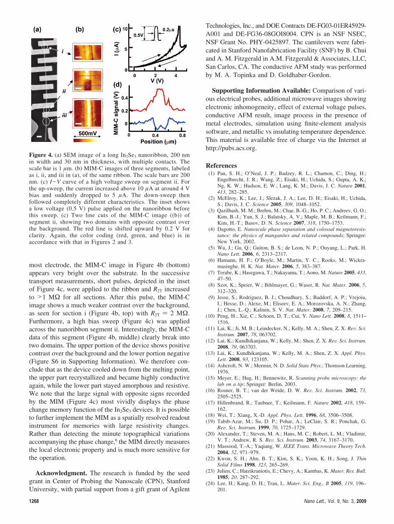
most electrode, the MIM-C image in Figure 4b (bottom)appears very bright over the substrate. In the successivetransport measurements, short pulses, depicted in the insetof Figure 4c, were applied to the ribbon and R2T increasedto >1 MΩ for all sections. After this pulse, the MIM-Cimage shows a much weaker contrast over the background,as seen for section i (Figure 4b, top) with R2T ) 2 MΩ.Furthermore, a high bias sweep (Figure 4c) was appliedacross the nanoribbon segment ii. Interestingly, the MIM-Cdata of this segment (Figure 4b, middle) clearly break intotwo domains. The upper portion of the device shows positivecontrast over the background and the lower portion negative(Figure S6 in Supporting Information). We therefore con-clude that as the device cooled down from the melting point,the upper part recrystallized and became highly conductiveagain, while the lower part stayed amorphous and resistive.We note that the large signal with opposite signs recordedby the MIM (Figure 4c) most vividly displays the phasechange memory function of the In2Se3 devices. It is possibleto further implement the MIM as a spatially resolved readoutinstrument for memories with large resistivity changes.Rather than detecting the minute topographical variationsaccompanying the phase change,6 the MIM directly measuresthe local electronic property and is much more sensitive forthe operation.
Acknowledgment. The research is funded by the seedgrant in Center of Probing the Nanoscale (CPN), StanfordUniversity, with partial support from a gift grant of Agilent
Technologies, Inc., and DOE Contracts DE-FG03-01ER45929-A001 and DE-FG36-08GOI8004. CPN is an NSF NSEC,NSF Grant No. PHY-0425897. The cantilevers were fabri-cated in Stanford Nanofabrication Facility (SNF) by B. Chuiand A. M. Fitzgerald in A.M. Fitzgerald & Associates, LLC,San Carlos, CA. The conductive AFM study was performedby M. A. Topinka and D. Goldhaber-Gordon.
Supporting Information Available: Comparison of vari-ous electrical probes, additional microwave images showingelectronic inhomogeneity, effect of external voltage pulses,conductive AFM result, image process in the presence ofmetal electrodes, simulation using finite-element analysissoftware, and metallic vs insulating temperature dependence.This material is available free of charge via the Internet athttp://pubs.acs.org.
References(1) Pan, S. H.; O’Neal, J. P.; Badzey, R. L.; Chamon, C.; Ding, H.;
Engelbrecht, J. R.; Wang, Z.; Eisaki, H.; Uchida, S.; Gupta, A. K.;Ng, K. W.; Hudson, E. W.; Lang, K. M.; Davis, J. C. Nature 2001,413, 282–285.
(2) McElroy, K.; Lee, J.; Slezak, J. A.; Lee, D. H.; Eisaki, H.; Uchida,S.; Davis, J. C. Science 2005, 309, 1048–1052.
(3) Qazilbash, M. M.; Brehm, M.; Chae, B.-G.; Ho, P. C.; Andreev, G. O.;Kim, B.-J.; Yun, S. J.; Balatsky, A. V.; Maple, M. B.; Keilmann, F.;Kim, H.-T.; Basov, D. N. Science 2007, 318, 1750–1753.
(4) Dagotto, E. Nanoscale phase separation and colossal magnetoresis-tance: the physics of manganites and related compounds; Springer:New York, 2002.
(5) Wu, J.; Gu, Q.; Guiton, B. S.; de Leon, N. P.; Ouyang, L.; Park, H.Nano Lett. 2006, 6, 2313–2317.
(6) Hamann, H. F.; O’Boyle, M.; Martin, Y. C.; Rooks, M.; Wickra-masinghe, H. K. Nat. Mater. 2006, 5, 383–387.
(7) Terabe, K.; Hasegawa, T.; Nakayama, T.; Aono, M. Nature 2005, 433,47–50.
(8) Szot, K.; Speier, W.; Bihlmayer, G.; Waser, R. Nat. Mater. 2006, 5,312–320.
(9) Jesse, S.; Rodriguez, B. J.; Choudhury, S.; Baddorf, A. P.; Vrejoiu,I.; Hesse, D.; Alexe, M.; Eliseev, E. A.; Morozovska, A. N.; Zhang,J.; Chen, L.-Q.; Kalinin, S. V. Nat. Mater. 2008, 7, 209–215.
(10) Peng, H.; Xie, C.; Schoen, D. T.; Cui, Y. Nano Lett. 2008, 8, 1511–1516.
(11) Lai, K.; Ji, M. B.; Leindecker, N.; Kelly, M. A.; Shen, Z. X. ReV. Sci.Instrum. 2007, 78, 063702.
(12) Lai, K.; Kundhikanjana, W.; Kelly, M.; Shen, Z. X. ReV. Sci. Instrum.2008, 79, 063703.
(13) Lai, K.; Kundhikanjana, W.; Kelly, M. A.; Shen, Z. X. Appl. Phys.Lett. 2008, 93, 123105.
(14) Ashcroft, N. W.; Mermin, N. D. Solid State Phys.; Thomson Learning,1976.
(15) Meyer, E.; Hug, H.; Bennewitz, R. Scanning probe microscopy: thelab on a tip; Springer: Berlin, 2003.
(16) Rosner, B. T.; van der Weide, D. W. ReV. Sci. Instrum. 2002, 73,2505–2525.
(17) Hillenbrand, R.; Taubner, T.; Keilmann, F. Nature 2002, 418, 159–162.
(18) Wei, T.; Xiang, X.-D. Appl. Phys. Lett. 1996, 68, 3506–3508.(19) Tabib-Azar, M.; Su, D. P.; Pohar, A.; LeClair, S. R.; Ponchak, G.
ReV. Sci. Instrum. 1999, 70, 1725–1729.(20) Alexander, T.; Steven, M. A.; Hans, M. C.; Robert, L. M.; Vladimir,
V. T.; Andrew, R. S. ReV. Sci. Instrum. 2003, 74, 3167–3170.(21) Massood, T.-A.; Yaqiang, W. IEEE Trans. MicrowaVe Theory Tech.
2004, 52, 971–979.(22) Kwon, S. H.; Ahn, B. T.; Kim, S. K.; Yoon, K. H.; Song, J. Thin
Solid Films 1998, 323, 265–269.(23) Julien, C.; Hatzikraniotis, E.; Chevy, A.; Kambas, K. Mater. Res. Bull.
1985, 20, 287–292.(24) Lee, H.; Kang, D. H.; Tran, L. Mater. Sci. Eng., B 2005, 119, 196–
201.
Figure 4. (a) SEM image of a long In2Se3 nanoribbon, 200 nmin width and 30 nm in thickness, with multiple contacts. Thescale bar is 1 µm. (b) MIM-C images of three segments, labeledas i, ii, and iii in (a), of the same ribbon. The scale bars are 200nm. (c) I-V curve of a high voltage sweep on segment ii. Forthe up-sweep, the current increased above 10 µA at around 4 Vbias and suddenly dropped to 5 µA. The down-sweep thenfollowed completely different characteristics. The inset showsa low voltage (0.5 V) pulse applied on the nanoribbon beforethis sweep. (c) Two line cuts of the MIM-C image ((b)) ofsegment ii, showing two domains with opposite contrast overthe background. The red line is shifted upward by 0.2 V forclarity. Again, the color coding (red, green, and blue) is inaccordance with that in Figures 2 and 3.
1268 Nano Lett., Vol. 9, No. 3, 2009

(25) Yu, B.; Ju, S. Y.; Sun, X. H.; Ng, G.; Nguyen, T. D.; Meyyappan,M.; Janes, D. B. Appl. Phys. Lett. 2007, 91, 133119.
(26) Ye, J. P.; Soeda, S.; Nakamura, Y.; Nittono, O. Jpn. J. Appl. Phys.,Part 1 1998, 37, 4264–4271.
(27) Peng, H. L.; Schoen, D. T.; Meister, S.; Zhang, X. F.; Cui, Y. J. Am.Chem. Soc. 2007, 129, 34–35.
(28) Two different growth directions, [0001] and [112j0], are found inour VLS-grown In2Se3 nanostructures. For simplicity, we onlydiscuss the results of nanoribbons with [112j0] growth direction,i.e., perpendicular to the normal direction of the layers.
(29) Only R2T is reported in the paper because the resistance of In2Se3
ribbons spans many orders of magnitude. For metallic ribbons, four-terminal measurements were also performed and it is confirmedthat the In/Au contact resistance is small (<1 kΩ) compared withthe sample resistance.
(30) Wang, Z.; Kelly, M. A.; Shen, Z.-X.; Shao, L.; Chu, W.-K.; Edwards,H. Appl. Phys. Lett. 2005, 86, 153118.
NL900222J
Nano Lett., Vol. 9, No. 3, 2009 1269