Nano Imaging Lab Services for Imaging and Analysis of ...
8
EINE INITIATIVE DER UNIVERSITÄT BASEL UND DES KANTONS AARGAU Nano Imaging Lab Services for Imaging and Analysis of Nanostructures Zinc oxide polymer
Transcript of Nano Imaging Lab Services for Imaging and Analysis of ...

EINE INITIATIVE DER UNIVERSITÄT BASELUND DES KANTONS AARGAU
Nano Imaging Lab Services for Imaging and Analysis of Nanostructures
Zinc oxide polymer

The Nano Imaging Lab
The Nano Imaging Lab (NI Lab) at Basel University’s Swiss Nanoscience Institute (SNI) offers a comprehensive service for imaging and analyzing nanostructures. The expe-rienced lab staff conducts an extensive range of microscopic analyses to internal and external clients alike. They offer everything from consulting and preparing samples to imaging.
Depending on the nature of the sample and the client’s needs, the NI Lab staff have decades of experience in investigating minute structures. Their varied range of equip-ment allows them both to precisely map and analyze surfaces, and to display inner structures down to atomic resolution.
The NI Lab trains researchers who regularly require this specialist imaging so that they can work independently with the various devices. The NI Lab also runs several courses each year for biology and nanoscience students, which have consistently been described as especially interesting.
Whether you are working in physics, material science, geology, biology, pharmaceutics, medicine or any other field, the Nano Imaging Lab will be happy to help and provide you with expert assistance whenever required.
The laboratories of the Nano Imaging Lab (at the Pharmacenter and the Physics Department of the University of Basel) suppplement each other and offer comprehensive and excellent imaging and analysis services.

Technologies in the Nano Imaging Lab
Investigating the topology of a sample
The Scanning Electron Microscope (SEM) is used to examine sample surfaces with secondary electrons (SE) and to create a topographical image. Back-scattered electrons (BSE) provide information about qualitative material composition. In the Cryo-SEM, shock-freezing can be applied to display aqueous samples without drying artifacts.
Atomic Force Microscopy (AFM) can characterize surfaces down to atomic resolution in different media including liquids. In contrast to SEM, a tip scans the surface of a sam-ple. Besides topography, it determines surface properties such as adhesion, elasticity, magnetic or electrostatic field distribution and surface conductivity.
SEM image of neuronal cultures grown on a CMOS (complementary metal-oxide-semiconductor) chip
AFM image of gold islands on a HOPG (highly oriented pyrolytic graphite) substrate
Identification and quantification of chemical composition
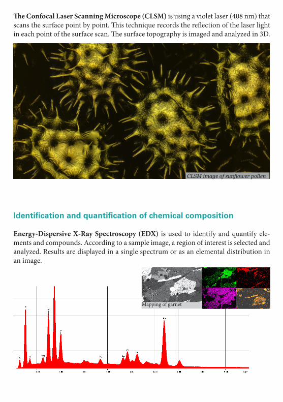
Energy-Dispersive X-Ray Spectroscopy (EDX) is used to identify and quantify ele-ments and compounds. According to a sample image, a region of interest is selected and analyzed. Results are displayed in a single spectrum or as an elemental distribution in an image.
The Confocal Laser Scanning Microscope (CLSM) is using a violet laser (408 nm) that scans the surface point by point. This technique records the reflection of the laser light in each point of the surface scan. The surface topography is imaged and analyzed in 3D.
CLSM image of sunflower pollen
Mapping of garnet

Manipulation of nano-scaled samples
Focused Ion Beam (FIB) technology is used to process nano samples. The ion beam is able to remove and cut material, so that the interior structures of an object can be analyzed. FIB allows, for example, to modify conductor paths and to measure the layer thickness. Fabrication of customized objects can also be performed.
FIB slice of carbon fiber
Investigating Nanoparticles up to atomic resolution
In Transmission Electron Microscopy (TEM) only thin and electron-transparent sam-ples can be analyzed. This provides insights into the inner life of an object. The expertise of the NI Lab is to reveal structures and functions of nanoparticles. A STEM attachment allows enhanced contrast imaging and EDX analysis.
TEM image of T4 phage
From Macroscopy to Nano Imaging
Correlative Light and Electron Microscopy (CLEM) uses different imaging technolo-gies applied to the same sample. Starting from a macroscopic image (e.g. light micros-copy), a region of interest on the sample is chosen and analyzed with a method of higher resolution (e.g. electron microscopy).
The Collaboration Process
• First contact via the homepage or admin tool (www.nanoimaging1.unibas.ch)• Discussion of the project• Preparation of sample material• Measurement with the appropriate microscopes• Documentation: Download via web interface
Costs
You find a detailed price list at: https://www.nanoscience.ch/en/services-2/nano-imaging-lab/prices/
Team of the Nano Imaging Lab
,
Markus Dürrenberger, Susanne Erpel, Daniel Mathys, Christian Schönenberger, Monica Schönenberger, and Eva Bieler

The Nano Imaging Lab is looking forward to fruitful collaborations
Nano Imaging LabSwiss Nanoscience InstituteUniversity of BaselPharmacenterKlingelbergstrasse 504056 BaselSwitzerlandTel.: +41 61 207 14 04
www.nanoimaging.unibas.ch
Nano Imaging Lab Equipment
Method Microscope• FIB/SEM/STEM FEI Helios Nanolab 650• SEM FEI Nova Nano SEM 230, Hitachi S4800 • SEM/Cryo-SEM Philips XL30 ESEM • TEM Philips CM100• AFM Bruker Dimension 3100, JPK NanoWizard®4, Nanosurf C3000• LSM Keyence VK-X200• Light microscopy Stereo microscopes
Preparation Methods
• Critical point drying• Ultra rapid freezing and high vacuum drying • Mechanical cutting and polishing• Ar plasma polishing and cutting• Plasma cleaning • Negative staining for TEM
University of Basel Petersplatz 1 P.O. Box 2148 4001 Basel Switzerland
www.unibas.ch
Educating Talentssince 1460.
Impressum
Text: Nano Imaging LabLayout: Nano Imaging Lab, C. Möller, M. WegmannDruck: Publikation Digital AG, BielMay 2019
© 2019 Swiss Nanoscience Institute, Nano Imaging LabBasel, Switzerland