
N5161A/62A/81A/82A/83A MXG Signal...
202
Agilent Technologies Agilent Technologies N5161A/62A/81A/82A/83A MXG Signal Generators Service Guide NOTICE: In August 2014, Agilent Technologies’ former Test and Measurement business became Keysight Technologies. This document is provided as a courtesy but is no longer kept current and thus will contain historical references to Agilent. For more information, go to www.keysight.com.
Transcript of N5161A/62A/81A/82A/83A MXG Signal...
Agilent Technologies
Agilent Technologies N5161A/62A/81A/82A/83A MXG Signal Generators
Service Guide
NOTICE: In August 2014, Agilent Technologies’ former Test and Measurement business became Keysight Technologies. This document is provided as a courtesy but is no longer kept current and thus will contain historical references to Agilent. For more information, go to www.keysight.com.
Service Guide
Notices© Agilent Technologies, Inc. 2006-2015No part of this manual may be reproduced in any form or by any means (including elec-tronic storage and retrieval or translation into a foreign language) without prior agree-ment and written consent from Agilent Technologies, Inc. as governed by United States and international copyright laws.
Manual Part NumberN5180-90006
EditionEdition 1, October 2015 Printed in USA
Agilent Technologies, Inc. 5301 Stevens Creek Blvd. Santa Clara, CA 95052 USA
Warranty
The material contained in this docu-ment is provided “as is,” and is sub-ject to being changed, without notice, in future editions. Further, to the max-imum extent permitted by applicable law, Agilent disclaims all warranties, either express or implied, with regard to this manual and any information contained herein, including but not limited to the implied warranties of merchantability and fitness for a par-ticular purpose. Agilent shall not be liable for errors or for incidental or consequential damages in connec-tion with the furnishing, use, or per-formance of this document or of any information contained herein. Should Agilent and the user have a separate written agreement with warranty terms covering the material in this document that conflict with these terms, the warranty terms in the sep-arate agreement shall control.
Technology Licenses The hardware and/or software described in this document are furnished under a license and may be used or copied only in accor-dance with the terms of such license.
Restricted Rights LegendU.S. Government Restricted Rights. Soft-ware and technical data rights granted to the federal government include only those rights customarily provided to end user cus-tomers. Agilent provides this customary commercial license in Software and techni-cal data pursuant to FAR 12.211 (Technical Data) and 12.212 (Computer Software) and, for the Department of Defense, DFARS 252.227-7015 (Technical Data - Commercial Items) and DFARS 227.7202-3 (Rights in Commercial Computer Software or Com-puter Software Documentation).
Safety Notices
CAUTION
A CAUTION notice denotes a haz-ard. It calls attention to an operat-ing procedure, practice, or the like that, if not correctly performed or adhered to, could result in damage to the product or loss of important data. Do not proceed beyond a CAUTION notice until the indicated conditions are fully understood and met.
WARNING
A WARNING notice denotes a hazard. It calls attention to an operating procedure, practice, or the like that, if not correctly per-formed or adhered to, could result in personal injury or death. Do not proceed beyond a WARNING notice until the indicated condi-tions are fully understood and met.
Service Guide
Contents
1. Troubleshooting
Before Troubleshooting . . . . . . . . . . . . . . . . . . . . . . . . . . . . . . . . . . . . . . . . . . . . . . . . . . . . . . . . . . . . . . . . . . . . . . . . . . . .1-1
ESD Information. . . . . . . . . . . . . . . . . . . . . . . . . . . . . . . . . . . . . . . . . . . . . . . . . . . . . . . . . . . . . . . . . . . . . . . . . . . . . .1-1
Contacting Agilent Technologies . . . . . . . . . . . . . . . . . . . . . . . . . . . . . . . . . . . . . . . . . . . . . . . . . . . . . . . . . . . . . . . . .1-2
Returning a Signal Generator for Service. . . . . . . . . . . . . . . . . . . . . . . . . . . . . . . . . . . . . . . . . . . . . . . . . . . . . . . . . . .1-2
Overall Block Description . . . . . . . . . . . . . . . . . . . . . . . . . . . . . . . . . . . . . . . . . . . . . . . . . . . . . . . . . . . . . . . . . . . . . . . . . .1-3
A1 Power Supply . . . . . . . . . . . . . . . . . . . . . . . . . . . . . . . . . . . . . . . . . . . . . . . . . . . . . . . . . . . . . . . . . . . . . . . . . . . . .1-3
A2 Vector Module (N5162A/82A Only) . . . . . . . . . . . . . . . . . . . . . . . . . . . . . . . . . . . . . . . . . . . . . . . . . . . . . . . . . . .1-3
A3 RF Assembly (N5161A/62A/81A/82A Only) . . . . . . . . . . . . . . . . . . . . . . . . . . . . . . . . . . . . . . . . . . . . . . . . . . . .1-3
A3 RF Assembly (N5183A Only) . . . . . . . . . . . . . . . . . . . . . . . . . . . . . . . . . . . . . . . . . . . . . . . . . . . . . . . . . . . . . . . .1-4
A4 Internal Memory Card (N5162A/82A Only) . . . . . . . . . . . . . . . . . . . . . . . . . . . . . . . . . . . . . . . . . . . . . . . . . . . . .1-5
A5 CPU. . . . . . . . . . . . . . . . . . . . . . . . . . . . . . . . . . . . . . . . . . . . . . . . . . . . . . . . . . . . . . . . . . . . . . . . . . . . . . . . . . . . .1-6
A6 Inverter Interface Board . . . . . . . . . . . . . . . . . . . . . . . . . . . . . . . . . . . . . . . . . . . . . . . . . . . . . . . . . . . . . . . . . . . . .1-6
A7 Micro Deck (N5183A Only) . . . . . . . . . . . . . . . . . . . . . . . . . . . . . . . . . . . . . . . . . . . . . . . . . . . . . . . . . . . . . . . . . .1-6
A8 Floating BNC Bypass (N5183A) . . . . . . . . . . . . . . . . . . . . . . . . . . . . . . . . . . . . . . . . . . . . . . . . . . . . . . . . . . . . . .1-7
A9 Interface Board (N5161A/62A) . . . . . . . . . . . . . . . . . . . . . . . . . . . . . . . . . . . . . . . . . . . . . . . . . . . . . . . . . . . . . . .1-7
Common Circuitry for the N5181A/82A/83A . . . . . . . . . . . . . . . . . . . . . . . . . . . . . . . . . . . . . . . . . . . . . . . . . . . . . . .1-7
Getting Started with Troubleshooting. . . . . . . . . . . . . . . . . . . . . . . . . . . . . . . . . . . . . . . . . . . . . . . . . . . . . . . . . . . . . . . . .1-13
Self Test Overview . . . . . . . . . . . . . . . . . . . . . . . . . . . . . . . . . . . . . . . . . . . . . . . . . . . . . . . . . . . . . . . . . . . . . . . . . . . . . . .1-15
Running Self Test . . . . . . . . . . . . . . . . . . . . . . . . . . . . . . . . . . . . . . . . . . . . . . . . . . . . . . . . . . . . . . . . . . . . . . . . . . . . . . . .1-16
Run Self Test Using the Front Panel (N518xA only) . . . . . . . . . . . . . . . . . . . . . . . . . . . . . . . . . . . . . . . . . . . . . . . . .1-16
Accessing the MXG Web-Enabled Page . . . . . . . . . . . . . . . . . . . . . . . . . . . . . . . . . . . . . . . . . . . . . . . . . . . . . . . . . .1-18
Self Tests Do Not Run or Self Tests Run Slowly . . . . . . . . . . . . . . . . . . . . . . . . . . . . . . . . . . . . . . . . . . . . . . . . . . . . . . . .1-19
Boot-up Routine . . . . . . . . . . . . . . . . . . . . . . . . . . . . . . . . . . . . . . . . . . . . . . . . . . . . . . . . . . . . . . . . . . . . . . . . . . . . . . . . .1-20
Troubleshooting Self Test 1105 . . . . . . . . . . . . . . . . . . . . . . . . . . . . . . . . . . . . . . . . . . . . . . . . . . . . . . . . . . . . . . . . . . . . .1-25
Troubleshooting Assembly Level Problems. . . . . . . . . . . . . . . . . . . . . . . . . . . . . . . . . . . . . . . . . . . . . . . . . . . . . . . . . . . .1-26
A1 Power Supply . . . . . . . . . . . . . . . . . . . . . . . . . . . . . . . . . . . . . . . . . . . . . . . . . . . . . . . . . . . . . . . . . . . . . . . . . . . .1-26
A2 Vector Module Troubleshooting (N5162A/82A Only) . . . . . . . . . . . . . . . . . . . . . . . . . . . . . . . . . . . . . . . . . . . . .1-29
A3 RF Assembly Troubleshooting . . . . . . . . . . . . . . . . . . . . . . . . . . . . . . . . . . . . . . . . . . . . . . . . . . . . . . . . . . . . . . .1-31
A4 Internal Memory Card Troubleshooting (N5162A/82A Only). . . . . . . . . . . . . . . . . . . . . . . . . . . . . . . . . . . . . . .1-32
A5 CPU Assembly Troubleshooting . . . . . . . . . . . . . . . . . . . . . . . . . . . . . . . . . . . . . . . . . . . . . . . . . . . . . . . . . . . . .1-33
A6 DC-AC Inverter Interface Board (N5181A/82A/83A) . . . . . . . . . . . . . . . . . . . . . . . . . . . . . . . . . . . . . . . . . . . . .1-34
A7 Micro Deck (N5183A) . . . . . . . . . . . . . . . . . . . . . . . . . . . . . . . . . . . . . . . . . . . . . . . . . . . . . . . . . . . . . . . . . . . . .1-36
A8 Floating BNC Bypass Troubleshooting (N5183A). . . . . . . . . . . . . . . . . . . . . . . . . . . . . . . . . . . . . . . . . . . . . . . .1-38
A9 Interface Board Troubleshooting (N5161A/62A). . . . . . . . . . . . . . . . . . . . . . . . . . . . . . . . . . . . . . . . . . . . . . . . .1-38
No Output Power or Output Power is Unleveled (N5183A) . . . . . . . . . . . . . . . . . . . . . . . . . . . . . . . . . . . . . . . . . . . . . . .1-40
Low Output Power or No Output Power < 3.2 GHz (N5183A) . . . . . . . . . . . . . . . . . . . . . . . . . . . . . . . . . . . . . . . . .1-41
Low Output Power or No Output Power >= 3.2 GHz (N5183A). . . . . . . . . . . . . . . . . . . . . . . . . . . . . . . . . . . . . . . .1-46
Checking ALC Operation < 3.2 GHz (N5183A) . . . . . . . . . . . . . . . . . . . . . . . . . . . . . . . . . . . . . . . . . . . . . . . . . . . . . . . .1-48
Amplitude Modulation Problems (N5183A) . . . . . . . . . . . . . . . . . . . . . . . . . . . . . . . . . . . . . . . . . . . . . . . . . . . . . . . . . . .1-50
Pulse Modulation Problems (N5183A). . . . . . . . . . . . . . . . . . . . . . . . . . . . . . . . . . . . . . . . . . . . . . . . . . . . . . . . . . . . . . . .1-51
LCD Display Appears to be Inoperative (Dark) . . . . . . . . . . . . . . . . . . . . . . . . . . . . . . . . . . . . . . . . . . . . . . . . . . . . . . . . .1-52
The Signal Generator Does Not Power On. . . . . . . . . . . . . . . . . . . . . . . . . . . . . . . . . . . . . . . . . . . . . . . . . . . . . . . . . . . . .1-52
All Front Panel LEDs are Not Functioning . . . . . . . . . . . . . . . . . . . . . . . . . . . . . . . . . . . . . . . . . . . . . . . . . . . . . . . . . . . .1-56
The Green Front Panel Power Switch LED or Yellow Standby LED is Not Working. . . . . . . . . . . . . . . . . . . . . . . . . . . .1-57
Front Panel Hardkeys or Softkeys are Not Functioning (N5181A/82A/83A) . . . . . . . . . . . . . . . . . . . . . . . . . . . . . . . . . .1-60
iii

Contents
The RPG Knob is Not Functioning (N5181A/82A/83A) . . . . . . . . . . . . . . . . . . . . . . . . . . . . . . . . . . . . . . . . . . . . . . . . . 1-60
Blank or Missing Pixels (N5181A/82A/83A) . . . . . . . . . . . . . . . . . . . . . . . . . . . . . . . . . . . . . . . . . . . . . . . . . . . . . . . . . 1-62
The Screen Saver is Not Functioning (N5181A/82A/83A) . . . . . . . . . . . . . . . . . . . . . . . . . . . . . . . . . . . . . . . . . . . . . . . 1-62
Boot Time Diagnostics Mode (N5161A/62A Only). . . . . . . . . . . . . . . . . . . . . . . . . . . . . . . . . . . . . . . . . . . . . . . . . . . . . 1-62
Exceptions - Auto-reboot, ERROR LED Blinking (N5161A/62A Only) . . . . . . . . . . . . . . . . . . . . . . . . . . . . . . . . 1-63
The Fans are Not Working . . . . . . . . . . . . . . . . . . . . . . . . . . . . . . . . . . . . . . . . . . . . . . . . . . . . . . . . . . . . . . . . . . . . . . . . 1-64
No LAN Activity . . . . . . . . . . . . . . . . . . . . . . . . . . . . . . . . . . . . . . . . . . . . . . . . . . . . . . . . . . . . . . . . . . . . . . . . . . . . . . . 1-64
No Front Panel USB Activity . . . . . . . . . . . . . . . . . . . . . . . . . . . . . . . . . . . . . . . . . . . . . . . . . . . . . . . . . . . . . . . . . . . . . . 1-64
No Rear-Panel USB Activity . . . . . . . . . . . . . . . . . . . . . . . . . . . . . . . . . . . . . . . . . . . . . . . . . . . . . . . . . . . . . . . . . . . . . . 1-64
No GPIB Activity . . . . . . . . . . . . . . . . . . . . . . . . . . . . . . . . . . . . . . . . . . . . . . . . . . . . . . . . . . . . . . . . . . . . . . . . . . . . . . . 1-65
Error Messages . . . . . . . . . . . . . . . . . . . . . . . . . . . . . . . . . . . . . . . . . . . . . . . . . . . . . . . . . . . . . . . . . . . . . . . . . . . . . . . . 1-65
Troubleshooting Unlocks . . . . . . . . . . . . . . . . . . . . . . . . . . . . . . . . . . . . . . . . . . . . . . . . . . . . . . . . . . . . . . . . . . . . . . . . . 1-65
508 Frac-N Loop Unlock . . . . . . . . . . . . . . . . . . . . . . . . . . . . . . . . . . . . . . . . . . . . . . . . . . . . . . . . . . . . . . . . . . . . . 1-65
512 Reference Unlocked. . . . . . . . . . . . . . . . . . . . . . . . . . . . . . . . . . . . . . . . . . . . . . . . . . . . . . . . . . . . . . . . . . . . . . 1-65
515 Reference Missing . . . . . . . . . . . . . . . . . . . . . . . . . . . . . . . . . . . . . . . . . . . . . . . . . . . . . . . . . . . . . . . . . . . . . . . 1-66
532 PCI Bridge FPGA DCM Unlocked . . . . . . . . . . . . . . . . . . . . . . . . . . . . . . . . . . . . . . . . . . . . . . . . . . . . . . . . . . 1-66
533 RF Analog FPGA DCM Unlocked . . . . . . . . . . . . . . . . . . . . . . . . . . . . . . . . . . . . . . . . . . . . . . . . . . . . . . . . . . 1-66
Troubleshooting Unlevels . . . . . . . . . . . . . . . . . . . . . . . . . . . . . . . . . . . . . . . . . . . . . . . . . . . . . . . . . . . . . . . . . . . . . . . . . 1-66
Troubleshooting the RF Path (N5161A/62A/81A/82A). . . . . . . . . . . . . . . . . . . . . . . . . . . . . . . . . . . . . . . . . . . . . . . . . . 1-68
Troubleshooting the 6 GHz Electronic Attenuator (N5161A/62A/81A/82A) . . . . . . . . . . . . . . . . . . . . . . . . . . . . . . . . . 1-68
Troubleshooting Harmonic Spurious . . . . . . . . . . . . . . . . . . . . . . . . . . . . . . . . . . . . . . . . . . . . . . . . . . . . . . . . . . . . . . . . 1-69
Troubleshooting Harmonic Spurious by Fundamental Frequency . . . . . . . . . . . . . . . . . . . . . . . . . . . . . . . . . . . . . 1-70
To Verify Harmonic Performance at the RF Output . . . . . . . . . . . . . . . . . . . . . . . . . . . . . . . . . . . . . . . . . . . . . . . . . 1-70
Troubleshooting Non-Harmonic Spurious . . . . . . . . . . . . . . . . . . . . . . . . . . . . . . . . . . . . . . . . . . . . . . . . . . . . . . . . . . . . 1-71
Troubleshooting Performance Test Problems . . . . . . . . . . . . . . . . . . . . . . . . . . . . . . . . . . . . . . . . . . . . . . . . . . . . . . . . . . 1-72
Manual Performance Test Problems . . . . . . . . . . . . . . . . . . . . . . . . . . . . . . . . . . . . . . . . . . . . . . . . . . . . . . . . . . . . . 1-72
Troubleshooting Adjustment Test Problems (N5183A Only) . . . . . . . . . . . . . . . . . . . . . . . . . . . . . . . . . . . . . . . . . 1-73
Automated Performance Test Problems . . . . . . . . . . . . . . . . . . . . . . . . . . . . . . . . . . . . . . . . . . . . . . . . . . . . . . . . . . 1-73
2. Replaceable Parts
Ordering Information . . . . . . . . . . . . . . . . . . . . . . . . . . . . . . . . . . . . . . . . . . . . . . . . . . . . . . . . . . . . . . . . . . . . . . . . . . . . . 2-1
Order Parts Fast . . . . . . . . . . . . . . . . . . . . . . . . . . . . . . . . . . . . . . . . . . . . . . . . . . . . . . . . . . . . . . . . . . . . . . . . . . . . . 2-1
Shipping a Defective Assembly Back to Agilent Technologies . . . . . . . . . . . . . . . . . . . . . . . . . . . . . . . . . . . . . . . . . . . . . 2-1
Frequency and Hardware Options . . . . . . . . . . . . . . . . . . . . . . . . . . . . . . . . . . . . . . . . . . . . . . . . . . . . . . . . . . . . . . . . . . . 2-2
Assemblies and Hardware Options. . . . . . . . . . . . . . . . . . . . . . . . . . . . . . . . . . . . . . . . . . . . . . . . . . . . . . . . . . . . . . . . . . . 2-3
Front Panel Assemblies (N5161A/62A only). . . . . . . . . . . . . . . . . . . . . . . . . . . . . . . . . . . . . . . . . . . . . . . . . . . . . . . 2-7
Front Panel Assemblies (N5181A/82A/83A only). . . . . . . . . . . . . . . . . . . . . . . . . . . . . . . . . . . . . . . . . . . . . . . . . . . 2-8
Assemblies from a Top View . . . . . . . . . . . . . . . . . . . . . . . . . . . . . . . . . . . . . . . . . . . . . . . . . . . . . . . . . . . . . . . . . . . 2-9
Assemblies from a Bottom View . . . . . . . . . . . . . . . . . . . . . . . . . . . . . . . . . . . . . . . . . . . . . . . . . . . . . . . . . . . . . . . 2-12
Cables . . . . . . . . . . . . . . . . . . . . . . . . . . . . . . . . . . . . . . . . . . . . . . . . . . . . . . . . . . . . . . . . . . . . . . . . . . . . . . . . . . . . . . . . 2-14
Cables from a Top View . . . . . . . . . . . . . . . . . . . . . . . . . . . . . . . . . . . . . . . . . . . . . . . . . . . . . . . . . . . . . . . . . . . . . . 2-16
Cables from a Bottom View . . . . . . . . . . . . . . . . . . . . . . . . . . . . . . . . . . . . . . . . . . . . . . . . . . . . . . . . . . . . . . . . . . . 2-19
Hardware . . . . . . . . . . . . . . . . . . . . . . . . . . . . . . . . . . . . . . . . . . . . . . . . . . . . . . . . . . . . . . . . . . . . . . . . . . . . . . . . . . . . . 2-21
Front Panel View . . . . . . . . . . . . . . . . . . . . . . . . . . . . . . . . . . . . . . . . . . . . . . . . . . . . . . . . . . . . . . . . . . . . . . . . . . . 2-21
Disassembled Rear Panel View . . . . . . . . . . . . . . . . . . . . . . . . . . . . . . . . . . . . . . . . . . . . . . . . . . . . . . . . . . . . . . . . 2-23
iv

Contents
Main Chassis with Inside Covers . . . . . . . . . . . . . . . . . . . . . . . . . . . . . . . . . . . . . . . . . . . . . . . . . . . . . . . . . . . . . . . .2-26
Outer Instrument Cover and Associated Parts . . . . . . . . . . . . . . . . . . . . . . . . . . . . . . . . . . . . . . . . . . . . . . . . . . . . . .2-27
Miscellaneous . . . . . . . . . . . . . . . . . . . . . . . . . . . . . . . . . . . . . . . . . . . . . . . . . . . . . . . . . . . . . . . . . . . . . . . . . . . . . . . . . . .2-29
Documentation . . . . . . . . . . . . . . . . . . . . . . . . . . . . . . . . . . . . . . . . . . . . . . . . . . . . . . . . . . . . . . . . . . . . . . . . . . . . . .2-29
Electrostatic Discharge (ESD) Protective Supplies . . . . . . . . . . . . . . . . . . . . . . . . . . . . . . . . . . . . . . . . . . . . . . . . . .2-29
Abbreviations Used in Part Descriptions . . . . . . . . . . . . . . . . . . . . . . . . . . . . . . . . . . . . . . . . . . . . . . . . . . . . . . . . . . . . . .2-30
3. Assembly Replacement
Before You Replace an Assembly . . . . . . . . . . . . . . . . . . . . . . . . . . . . . . . . . . . . . . . . . . . . . . . . . . . . . . . . . . . . . . . . . . . .3-1
After Replacing or Repairing an Assembly . . . . . . . . . . . . . . . . . . . . . . . . . . . . . . . . . . . . . . . . . . . . . . . . . . . . . . . . . . . . .3-1
Assemblies You Can Replace . . . . . . . . . . . . . . . . . . . . . . . . . . . . . . . . . . . . . . . . . . . . . . . . . . . . . . . . . . . . . . . . . . . . . . . .3-1
Outer Cover. . . . . . . . . . . . . . . . . . . . . . . . . . . . . . . . . . . . . . . . . . . . . . . . . . . . . . . . . . . . . . . . . . . . . . . . . . . . . . . . . . . . . .3-4
Tools Required . . . . . . . . . . . . . . . . . . . . . . . . . . . . . . . . . . . . . . . . . . . . . . . . . . . . . . . . . . . . . . . . . . . . . . . . . . . . . . .3-4
Removal Procedure. . . . . . . . . . . . . . . . . . . . . . . . . . . . . . . . . . . . . . . . . . . . . . . . . . . . . . . . . . . . . . . . . . . . . . . . . . . .3-4
Replacement Procedure . . . . . . . . . . . . . . . . . . . . . . . . . . . . . . . . . . . . . . . . . . . . . . . . . . . . . . . . . . . . . . . . . . . . . . . .3-4
Inner Top Cover . . . . . . . . . . . . . . . . . . . . . . . . . . . . . . . . . . . . . . . . . . . . . . . . . . . . . . . . . . . . . . . . . . . . . . . . . . . . . . . . . .3-6
Tools Required . . . . . . . . . . . . . . . . . . . . . . . . . . . . . . . . . . . . . . . . . . . . . . . . . . . . . . . . . . . . . . . . . . . . . . . . . . . . . . .3-6
Removal Procedure . . . . . . . . . . . . . . . . . . . . . . . . . . . . . . . . . . . . . . . . . . . . . . . . . . . . . . . . . . . . . . . . . . . . . . . . . . .3-6
Replacement Procedure . . . . . . . . . . . . . . . . . . . . . . . . . . . . . . . . . . . . . . . . . . . . . . . . . . . . . . . . . . . . . . . . . . . . . . . .3-6
Inner Bottom Cover . . . . . . . . . . . . . . . . . . . . . . . . . . . . . . . . . . . . . . . . . . . . . . . . . . . . . . . . . . . . . . . . . . . . . . . . . . . . . . .3-8
Tools Required . . . . . . . . . . . . . . . . . . . . . . . . . . . . . . . . . . . . . . . . . . . . . . . . . . . . . . . . . . . . . . . . . . . . . . . . . . . . . . .3-8
Removal Procedure . . . . . . . . . . . . . . . . . . . . . . . . . . . . . . . . . . . . . . . . . . . . . . . . . . . . . . . . . . . . . . . . . . . . . . . . . . .3-8
Replacement Procedure . . . . . . . . . . . . . . . . . . . . . . . . . . . . . . . . . . . . . . . . . . . . . . . . . . . . . . . . . . . . . . . . . . . . . . . .3-8
Front-Panel . . . . . . . . . . . . . . . . . . . . . . . . . . . . . . . . . . . . . . . . . . . . . . . . . . . . . . . . . . . . . . . . . . . . . . . . . . . . . . . . . . . . .3-10
Tools Required . . . . . . . . . . . . . . . . . . . . . . . . . . . . . . . . . . . . . . . . . . . . . . . . . . . . . . . . . . . . . . . . . . . . . . . . . . . . . .3-10
Removal Procedure. . . . . . . . . . . . . . . . . . . . . . . . . . . . . . . . . . . . . . . . . . . . . . . . . . . . . . . . . . . . . . . . . . . . . . . . . . .3-10
Replacement Procedure . . . . . . . . . . . . . . . . . . . . . . . . . . . . . . . . . . . . . . . . . . . . . . . . . . . . . . . . . . . . . . . . . . . . . . .3-10
USB Board . . . . . . . . . . . . . . . . . . . . . . . . . . . . . . . . . . . . . . . . . . . . . . . . . . . . . . . . . . . . . . . . . . . . . . . . . . . . . . . . . . . . .3-12
Tools Required . . . . . . . . . . . . . . . . . . . . . . . . . . . . . . . . . . . . . . . . . . . . . . . . . . . . . . . . . . . . . . . . . . . . . . . . . . . . . .3-12
Removal Procedure. . . . . . . . . . . . . . . . . . . . . . . . . . . . . . . . . . . . . . . . . . . . . . . . . . . . . . . . . . . . . . . . . . . . . . . . . . .3-12
Replacement Procedure . . . . . . . . . . . . . . . . . . . . . . . . . . . . . . . . . . . . . . . . . . . . . . . . . . . . . . . . . . . . . . . . . . . . . . .3-12
LCD Display (N5181A/82A/83A only) . . . . . . . . . . . . . . . . . . . . . . . . . . . . . . . . . . . . . . . . . . . . . . . . . . . . . . . . . . . . . . .3-14
Tools Required . . . . . . . . . . . . . . . . . . . . . . . . . . . . . . . . . . . . . . . . . . . . . . . . . . . . . . . . . . . . . . . . . . . . . . . . . . . . . .3-14
Removal Procedure. . . . . . . . . . . . . . . . . . . . . . . . . . . . . . . . . . . . . . . . . . . . . . . . . . . . . . . . . . . . . . . . . . . . . . . . . . .3-14
Replacement Procedure . . . . . . . . . . . . . . . . . . . . . . . . . . . . . . . . . . . . . . . . . . . . . . . . . . . . . . . . . . . . . . . . . . . . . . .3-14
A6 DC-AC Inverter Interface Board (N5181A/82A/83A only) . . . . . . . . . . . . . . . . . . . . . . . . . . . . . . . . . . . . . . . . . . . . .3-16
Tools Required . . . . . . . . . . . . . . . . . . . . . . . . . . . . . . . . . . . . . . . . . . . . . . . . . . . . . . . . . . . . . . . . . . . . . . . . . . . . . .3-16
Removal Procedure. . . . . . . . . . . . . . . . . . . . . . . . . . . . . . . . . . . . . . . . . . . . . . . . . . . . . . . . . . . . . . . . . . . . . . . . . . .3-16
Replacement Procedure . . . . . . . . . . . . . . . . . . . . . . . . . . . . . . . . . . . . . . . . . . . . . . . . . . . . . . . . . . . . . . . . . . . . . . .3-16
A9 Interface Board (N5161A/62A only) . . . . . . . . . . . . . . . . . . . . . . . . . . . . . . . . . . . . . . . . . . . . . . . . . . . . . . . . . . . . . .3-18
Tools Required . . . . . . . . . . . . . . . . . . . . . . . . . . . . . . . . . . . . . . . . . . . . . . . . . . . . . . . . . . . . . . . . . . . . . . . . . . . . . .3-18
Removal Procedure. . . . . . . . . . . . . . . . . . . . . . . . . . . . . . . . . . . . . . . . . . . . . . . . . . . . . . . . . . . . . . . . . . . . . . . . . . .3-18
Replacement Procedure . . . . . . . . . . . . . . . . . . . . . . . . . . . . . . . . . . . . . . . . . . . . . . . . . . . . . . . . . . . . . . . . . . . . . . .3-18
Key Pad (N5181A/82A/83A only) . . . . . . . . . . . . . . . . . . . . . . . . . . . . . . . . . . . . . . . . . . . . . . . . . . . . . . . . . . . . . . . . . . .3-20
Tools Required . . . . . . . . . . . . . . . . . . . . . . . . . . . . . . . . . . . . . . . . . . . . . . . . . . . . . . . . . . . . . . . . . . . . . . . . . . . . . .3-20
Removal Procedure. . . . . . . . . . . . . . . . . . . . . . . . . . . . . . . . . . . . . . . . . . . . . . . . . . . . . . . . . . . . . . . . . . . . . . . . . . .3-20
v

Contents
Replacement Procedure . . . . . . . . . . . . . . . . . . . . . . . . . . . . . . . . . . . . . . . . . . . . . . . . . . . . . . . . . . . . . . . . . . . . . . 3-20
Power Switch . . . . . . . . . . . . . . . . . . . . . . . . . . . . . . . . . . . . . . . . . . . . . . . . . . . . . . . . . . . . . . . . . . . . . . . . . . . . . . . . . . 3-21
Tools Required . . . . . . . . . . . . . . . . . . . . . . . . . . . . . . . . . . . . . . . . . . . . . . . . . . . . . . . . . . . . . . . . . . . . . . . . . . . . . 3-21
Removal Procedure. . . . . . . . . . . . . . . . . . . . . . . . . . . . . . . . . . . . . . . . . . . . . . . . . . . . . . . . . . . . . . . . . . . . . . . . . . 3-21
Replacement Procedure . . . . . . . . . . . . . . . . . . . . . . . . . . . . . . . . . . . . . . . . . . . . . . . . . . . . . . . . . . . . . . . . . . . . . . 3-21
Rear Panel (N5161A/81A) . . . . . . . . . . . . . . . . . . . . . . . . . . . . . . . . . . . . . . . . . . . . . . . . . . . . . . . . . . . . . . . . . . . . . . . . 3-22
Tools Required . . . . . . . . . . . . . . . . . . . . . . . . . . . . . . . . . . . . . . . . . . . . . . . . . . . . . . . . . . . . . . . . . . . . . . . . . . . . . 3-22
Removal Procedure. . . . . . . . . . . . . . . . . . . . . . . . . . . . . . . . . . . . . . . . . . . . . . . . . . . . . . . . . . . . . . . . . . . . . . . . . . 3-22
Replacement Procedure . . . . . . . . . . . . . . . . . . . . . . . . . . . . . . . . . . . . . . . . . . . . . . . . . . . . . . . . . . . . . . . . . . . . . . 3-22
Rear Panel (N5162A/82A) . . . . . . . . . . . . . . . . . . . . . . . . . . . . . . . . . . . . . . . . . . . . . . . . . . . . . . . . . . . . . . . . . . . . . . . . 3-24
Tools Required . . . . . . . . . . . . . . . . . . . . . . . . . . . . . . . . . . . . . . . . . . . . . . . . . . . . . . . . . . . . . . . . . . . . . . . . . . . . . 3-24
Removal Procedure. . . . . . . . . . . . . . . . . . . . . . . . . . . . . . . . . . . . . . . . . . . . . . . . . . . . . . . . . . . . . . . . . . . . . . . . . . 3-24
Replacement Procedure . . . . . . . . . . . . . . . . . . . . . . . . . . . . . . . . . . . . . . . . . . . . . . . . . . . . . . . . . . . . . . . . . . . . . . 3-24
Rear Panel (N5183A) . . . . . . . . . . . . . . . . . . . . . . . . . . . . . . . . . . . . . . . . . . . . . . . . . . . . . . . . . . . . . . . . . . . . . . . . . . . . 3-26
Tools Required . . . . . . . . . . . . . . . . . . . . . . . . . . . . . . . . . . . . . . . . . . . . . . . . . . . . . . . . . . . . . . . . . . . . . . . . . . . . . 3-26
Removal Procedure. . . . . . . . . . . . . . . . . . . . . . . . . . . . . . . . . . . . . . . . . . . . . . . . . . . . . . . . . . . . . . . . . . . . . . . . . . 3-26
Replacement Procedure . . . . . . . . . . . . . . . . . . . . . . . . . . . . . . . . . . . . . . . . . . . . . . . . . . . . . . . . . . . . . . . . . . . . . . 3-26
A1 Power Supply . . . . . . . . . . . . . . . . . . . . . . . . . . . . . . . . . . . . . . . . . . . . . . . . . . . . . . . . . . . . . . . . . . . . . . . . . . . . . . . 3-28
Tools Required . . . . . . . . . . . . . . . . . . . . . . . . . . . . . . . . . . . . . . . . . . . . . . . . . . . . . . . . . . . . . . . . . . . . . . . . . . . . . 3-28
Removal Procedure . . . . . . . . . . . . . . . . . . . . . . . . . . . . . . . . . . . . . . . . . . . . . . . . . . . . . . . . . . . . . . . . . . . . . . . . . 3-28
Replacement Procedure . . . . . . . . . . . . . . . . . . . . . . . . . . . . . . . . . . . . . . . . . . . . . . . . . . . . . . . . . . . . . . . . . . . . . . 3-28
A2 Vector Module (N5162A with Option 012 and N5182A Option 1EM with Option 012) . . . . . . . . . . . . . . . . . . . . . 3-30
Tools Required . . . . . . . . . . . . . . . . . . . . . . . . . . . . . . . . . . . . . . . . . . . . . . . . . . . . . . . . . . . . . . . . . . . . . . . . . . . . . 3-30
Removal Procedure. . . . . . . . . . . . . . . . . . . . . . . . . . . . . . . . . . . . . . . . . . . . . . . . . . . . . . . . . . . . . . . . . . . . . . . . . . 3-30
Replacement Procedure . . . . . . . . . . . . . . . . . . . . . . . . . . . . . . . . . . . . . . . . . . . . . . . . . . . . . . . . . . . . . . . . . . . . . . 3-30
A2 Vector Module (N5162A/82A without Option 012). . . . . . . . . . . . . . . . . . . . . . . . . . . . . . . . . . . . . . . . . . . . . . . . . . 3-32
Tools Required . . . . . . . . . . . . . . . . . . . . . . . . . . . . . . . . . . . . . . . . . . . . . . . . . . . . . . . . . . . . . . . . . . . . . . . . . . . . . 3-32
Removal Procedure. . . . . . . . . . . . . . . . . . . . . . . . . . . . . . . . . . . . . . . . . . . . . . . . . . . . . . . . . . . . . . . . . . . . . . . . . . 3-32
Replacement Procedure . . . . . . . . . . . . . . . . . . . . . . . . . . . . . . . . . . . . . . . . . . . . . . . . . . . . . . . . . . . . . . . . . . . . . . 3-32
A3 RF Assembly (N5162A, with and without Option 012, N5182A with Option 012, and N5182A Option 1EM, with and without Option 012) . . . . . . . . . . . . . . . . . . . . . . . . . . . . . . . . . . . . . . . . . . . . . . . . . . . . . . . . . . . . . . . . . . . . . . . . . . . . . 3-34
Tools Required . . . . . . . . . . . . . . . . . . . . . . . . . . . . . . . . . . . . . . . . . . . . . . . . . . . . . . . . . . . . . . . . . . . . . . . . . . . . . 3-34
Removal Procedure. . . . . . . . . . . . . . . . . . . . . . . . . . . . . . . . . . . . . . . . . . . . . . . . . . . . . . . . . . . . . . . . . . . . . . . . . . 3-34
Replacement Procedure . . . . . . . . . . . . . . . . . . . . . . . . . . . . . . . . . . . . . . . . . . . . . . . . . . . . . . . . . . . . . . . . . . . . . . 3-34
A3 RF Assembly - Standard (N5181A/82A) . . . . . . . . . . . . . . . . . . . . . . . . . . . . . . . . . . . . . . . . . . . . . . . . . . . . . . . . . . 3-38
Tools Required . . . . . . . . . . . . . . . . . . . . . . . . . . . . . . . . . . . . . . . . . . . . . . . . . . . . . . . . . . . . . . . . . . . . . . . . . . . . . 3-38
Removal Procedure. . . . . . . . . . . . . . . . . . . . . . . . . . . . . . . . . . . . . . . . . . . . . . . . . . . . . . . . . . . . . . . . . . . . . . . . . . 3-38
Replacement Procedure . . . . . . . . . . . . . . . . . . . . . . . . . . . . . . . . . . . . . . . . . . . . . . . . . . . . . . . . . . . . . . . . . . . . . . 3-38
A3 RF Assembly - N5161A and N5181A Option 1EM. . . . . . . . . . . . . . . . . . . . . . . . . . . . . . . . . . . . . . . . . . . . . . . . . . 3-42
Tools Required . . . . . . . . . . . . . . . . . . . . . . . . . . . . . . . . . . . . . . . . . . . . . . . . . . . . . . . . . . . . . . . . . . . . . . . . . . . . . 3-42
Removal Procedure. . . . . . . . . . . . . . . . . . . . . . . . . . . . . . . . . . . . . . . . . . . . . . . . . . . . . . . . . . . . . . . . . . . . . . . . . . 3-42
Replacement Procedure . . . . . . . . . . . . . . . . . . . . . . . . . . . . . . . . . . . . . . . . . . . . . . . . . . . . . . . . . . . . . . . . . . . . . . 3-42
A3 RF Assembly (N5183A only) . . . . . . . . . . . . . . . . . . . . . . . . . . . . . . . . . . . . . . . . . . . . . . . . . . . . . . . . . . . . . . . . . . . 3-46
Tools Required . . . . . . . . . . . . . . . . . . . . . . . . . . . . . . . . . . . . . . . . . . . . . . . . . . . . . . . . . . . . . . . . . . . . . . . . . . . . . 3-46
Removal Procedure. . . . . . . . . . . . . . . . . . . . . . . . . . . . . . . . . . . . . . . . . . . . . . . . . . . . . . . . . . . . . . . . . . . . . . . . . . 3-46
Replacement Procedure . . . . . . . . . . . . . . . . . . . . . . . . . . . . . . . . . . . . . . . . . . . . . . . . . . . . . . . . . . . . . . . . . . . . . . 3-46
A3BT1 Battery . . . . . . . . . . . . . . . . . . . . . . . . . . . . . . . . . . . . . . . . . . . . . . . . . . . . . . . . . . . . . . . . . . . . . . . . . . . . . . . . . 3-50
vi

Contents
Tools Required . . . . . . . . . . . . . . . . . . . . . . . . . . . . . . . . . . . . . . . . . . . . . . . . . . . . . . . . . . . . . . . . . . . . . . . . . . . . . .3-50
Removal Procedure . . . . . . . . . . . . . . . . . . . . . . . . . . . . . . . . . . . . . . . . . . . . . . . . . . . . . . . . . . . . . . . . . . . . . . . . . .3-50
Replacement Procedure . . . . . . . . . . . . . . . . . . . . . . . . . . . . . . . . . . . . . . . . . . . . . . . . . . . . . . . . . . . . . . . . . . . . . . .3-50
A4 Internal Memory Card (N5162A/82A only) . . . . . . . . . . . . . . . . . . . . . . . . . . . . . . . . . . . . . . . . . . . . . . . . . . . . . . . . .3-52
Tools Required . . . . . . . . . . . . . . . . . . . . . . . . . . . . . . . . . . . . . . . . . . . . . . . . . . . . . . . . . . . . . . . . . . . . . . . . . . . . . .3-52
Removal Procedure . . . . . . . . . . . . . . . . . . . . . . . . . . . . . . . . . . . . . . . . . . . . . . . . . . . . . . . . . . . . . . . . . . . . . . . . . .3-52
Replacement Procedure . . . . . . . . . . . . . . . . . . . . . . . . . . . . . . . . . . . . . . . . . . . . . . . . . . . . . . . . . . . . . . . . . . . . . . .3-52
A5 CPU. . . . . . . . . . . . . . . . . . . . . . . . . . . . . . . . . . . . . . . . . . . . . . . . . . . . . . . . . . . . . . . . . . . . . . . . . . . . . . . . . . . . . . . .3-54
Tools Required . . . . . . . . . . . . . . . . . . . . . . . . . . . . . . . . . . . . . . . . . . . . . . . . . . . . . . . . . . . . . . . . . . . . . . . . . . . . . .3-54
Removal Procedure . . . . . . . . . . . . . . . . . . . . . . . . . . . . . . . . . . . . . . . . . . . . . . . . . . . . . . . . . . . . . . . . . . . . . . . . . .3-54
Replacement Procedure . . . . . . . . . . . . . . . . . . . . . . . . . . . . . . . . . . . . . . . . . . . . . . . . . . . . . . . . . . . . . . . . . . . . . . .3-54
A7 Micro-Deck (N5183A only - Standard) . . . . . . . . . . . . . . . . . . . . . . . . . . . . . . . . . . . . . . . . . . . . . . . . . . . . . . . . . . . .3-56
Tools Required . . . . . . . . . . . . . . . . . . . . . . . . . . . . . . . . . . . . . . . . . . . . . . . . . . . . . . . . . . . . . . . . . . . . . . . . . . . . . .3-56
Removal Procedure. . . . . . . . . . . . . . . . . . . . . . . . . . . . . . . . . . . . . . . . . . . . . . . . . . . . . . . . . . . . . . . . . . . . . . . . . . .3-56
Replacement Procedure . . . . . . . . . . . . . . . . . . . . . . . . . . . . . . . . . . . . . . . . . . . . . . . . . . . . . . . . . . . . . . . . . . . . . . .3-56
A7 Micro-Deck (N5183A only - Option 1EM) . . . . . . . . . . . . . . . . . . . . . . . . . . . . . . . . . . . . . . . . . . . . . . . . . . . . . . . . .3-59
Tools Required . . . . . . . . . . . . . . . . . . . . . . . . . . . . . . . . . . . . . . . . . . . . . . . . . . . . . . . . . . . . . . . . . . . . . . . . . . . . . .3-59
Removal Procedure. . . . . . . . . . . . . . . . . . . . . . . . . . . . . . . . . . . . . . . . . . . . . . . . . . . . . . . . . . . . . . . . . . . . . . . . . . .3-59
Replacement Procedure . . . . . . . . . . . . . . . . . . . . . . . . . . . . . . . . . . . . . . . . . . . . . . . . . . . . . . . . . . . . . . . . . . . . . . .3-59
A8 Floating BNC Bypass (N5183A only) . . . . . . . . . . . . . . . . . . . . . . . . . . . . . . . . . . . . . . . . . . . . . . . . . . . . . . . . . . . . .3-62
Tools Required . . . . . . . . . . . . . . . . . . . . . . . . . . . . . . . . . . . . . . . . . . . . . . . . . . . . . . . . . . . . . . . . . . . . . . . . . . . . . .3-62
Removal Procedure. . . . . . . . . . . . . . . . . . . . . . . . . . . . . . . . . . . . . . . . . . . . . . . . . . . . . . . . . . . . . . . . . . . . . . . . . . .3-62
Replacement Procedure . . . . . . . . . . . . . . . . . . . . . . . . . . . . . . . . . . . . . . . . . . . . . . . . . . . . . . . . . . . . . . . . . . . . . . .3-62
RF Connector (N5183A only - Standard). . . . . . . . . . . . . . . . . . . . . . . . . . . . . . . . . . . . . . . . . . . . . . . . . . . . . . . . . . . . . .3-64
Tools Required . . . . . . . . . . . . . . . . . . . . . . . . . . . . . . . . . . . . . . . . . . . . . . . . . . . . . . . . . . . . . . . . . . . . . . . . . . . . . .3-64
Removal Procedure. . . . . . . . . . . . . . . . . . . . . . . . . . . . . . . . . . . . . . . . . . . . . . . . . . . . . . . . . . . . . . . . . . . . . . . . . . .3-64
Replacement Procedure . . . . . . . . . . . . . . . . . . . . . . . . . . . . . . . . . . . . . . . . . . . . . . . . . . . . . . . . . . . . . . . . . . . . . . .3-64
B1 thru B4 Fans . . . . . . . . . . . . . . . . . . . . . . . . . . . . . . . . . . . . . . . . . . . . . . . . . . . . . . . . . . . . . . . . . . . . . . . . . . . . . . . . .3-66
Tools Required . . . . . . . . . . . . . . . . . . . . . . . . . . . . . . . . . . . . . . . . . . . . . . . . . . . . . . . . . . . . . . . . . . . . . . . . . . . . . .3-66
Removal Procedure. . . . . . . . . . . . . . . . . . . . . . . . . . . . . . . . . . . . . . . . . . . . . . . . . . . . . . . . . . . . . . . . . . . . . . . . . . .3-66
Replacement Procedure . . . . . . . . . . . . . . . . . . . . . . . . . . . . . . . . . . . . . . . . . . . . . . . . . . . . . . . . . . . . . . . . . . . . . . .3-66
4. Post-Repair Procedures and Performance Verification
Post Repair Procedures . . . . . . . . . . . . . . . . . . . . . . . . . . . . . . . . . . . . . . . . . . . . . . . . . . . . . . . . . . . . . . . . . . . . . . . . . . . . .3-1
Assembly Installation and Removal Overview . . . . . . . . . . . . . . . . . . . . . . . . . . . . . . . . . . . . . . . . . . . . . . . . . . . . . .3-2
Service Procedure . . . . . . . . . . . . . . . . . . . . . . . . . . . . . . . . . . . . . . . . . . . . . . . . . . . . . . . . . . . . . . . . . . . . . . . . . . . . .3-3
Post-Repair Overview. . . . . . . . . . . . . . . . . . . . . . . . . . . . . . . . . . . . . . . . . . . . . . . . . . . . . . . . . . . . . . . . . . . . . . . . . .3-4
Manual Performance Tests . . . . . . . . . . . . . . . . . . . . . . . . . . . . . . . . . . . . . . . . . . . . . . . . . . . . . . . . . . . . . . . . . . . . . .3-4
Adjustments (N5183A Only) . . . . . . . . . . . . . . . . . . . . . . . . . . . . . . . . . . . . . . . . . . . . . . . . . . . . . . . . . . . . . . . . . . . .3-6
Automated Performance Verification Tests . . . . . . . . . . . . . . . . . . . . . . . . . . . . . . . . . . . . . . . . . . . . . . . . . . . . . . . . .3-6
Performance Verification . . . . . . . . . . . . . . . . . . . . . . . . . . . . . . . . . . . . . . . . . . . . . . . . . . . . . . . . . . . . . . . . . . . . . . . . . . .3-8
I/Q Calibration (N5162A/82A only). . . . . . . . . . . . . . . . . . . . . . . . . . . . . . . . . . . . . . . . . . . . . . . . . . . . . . . . . . . . . . . . . . .3-8
Running Self Test . . . . . . . . . . . . . . . . . . . . . . . . . . . . . . . . . . . . . . . . . . . . . . . . . . . . . . . . . . . . . . . . . . . . . . . . . . . . . . . . .3-8
Self Test Failure . . . . . . . . . . . . . . . . . . . . . . . . . . . . . . . . . . . . . . . . . . . . . . . . . . . . . . . . . . . . . . . . . . . . . . . . . . . . . .3-9
Relative Frequency Range and Accuracy Verification (N5161A/62A1/81A/82A Only) . . . . . . . . . . . . . . . . . . . . . . . . . .3-10
Frequency Counter Procedure (N5161A/62A/81A/82A) . . . . . . . . . . . . . . . . . . . . . . . . . . . . . . . . . . . . . . . . . . . . . .3-10
vii

Contents
Spectrum Analyzer Procedure (N5161A/62A1/81A/82A) . . . . . . . . . . . . . . . . . . . . . . . . . . . . . . . . . . . . . . . . . . . . .3-11
Leveled Output Power Verification (N5161A/62A1/81A/82A Only) . . . . . . . . . . . . . . . . . . . . . . . . . . . . . . . . . . . . . . . 3-13
N5161A1/81A Output Power Test Procedure . . . . . . . . . . . . . . . . . . . . . . . . . . . . . . . . . . . . . . . . . . . . . . . . . . . . . . 3-13
N5162A/82A Output Power Test Procedure. . . . . . . . . . . . . . . . . . . . . . . . . . . . . . . . . . . . . . . . . . . . . . . . . . . . . . . 3-15
5. Safety and Regulatory
General Safety Considerations . . . . . . . . . . . . . . . . . . . . . . . . . . . . . . . . . . . . . . . . . . . . . . . . . . . . . . . . . . . . . . . . . . . . . . 4-1
Lithium Battery Disposal . . . . . . . . . . . . . . . . . . . . . . . . . . . . . . . . . . . . . . . . . . . . . . . . . . . . . . . . . . . . . . . . . . . . . . . . . . 4-2
Assistance . . . . . . . . . . . . . . . . . . . . . . . . . . . . . . . . . . . . . . . . . . . . . . . . . . . . . . . . . . . . . . . . . . . . . . . . . . . . . . . . . . . . . . 4-2
Certification . . . . . . . . . . . . . . . . . . . . . . . . . . . . . . . . . . . . . . . . . . . . . . . . . . . . . . . . . . . . . . . . . . . . . . . . . . . . . . . . . . . . 4-2
6. Instrument History
How to Use this Chapter . . . . . . . . . . . . . . . . . . . . . . . . . . . . . . . . . . . . . . . . . . . . . . . . . . . . . . . . . . . . . . . . . . . . . . . . . . . 6-1
September 2009 . . . . . . . . . . . . . . . . . . . . . . . . . . . . . . . . . . . . . . . . . . . . . . . . . . . . . . . . . . . . . . . . . . . . . . . . . . . . . . . . . 6-1
January 2009 (N5161A/62A/81A/82A/83A only) . . . . . . . . . . . . . . . . . . . . . . . . . . . . . . . . . . . . . . . . . . . . . . . . . . . . . . . 6-1
August 2008 (N5161A/62A/81A/82A/83A only) . . . . . . . . . . . . . . . . . . . . . . . . . . . . . . . . . . . . . . . . . . . . . . . . . . . . . . . 6-1
April 2008 (N5182A/83A only) . . . . . . . . . . . . . . . . . . . . . . . . . . . . . . . . . . . . . . . . . . . . . . . . . . . . . . . . . . . . . . . . . . . . . 6-1
December 2007 . . . . . . . . . . . . . . . . . . . . . . . . . . . . . . . . . . . . . . . . . . . . . . . . . . . . . . . . . . . . . . . . . . . . . . . . . . . . . . . . . . 6-1
November 2007. . . . . . . . . . . . . . . . . . . . . . . . . . . . . . . . . . . . . . . . . . . . . . . . . . . . . . . . . . . . . . . . . . . . . . . . . . . . . . . . . . 6-1
October 2007 (N5181A/82A only) . . . . . . . . . . . . . . . . . . . . . . . . . . . . . . . . . . . . . . . . . . . . . . . . . . . . . . . . . . . . . . . . . . . 6-1
May 2007 (N5181A/82A only). . . . . . . . . . . . . . . . . . . . . . . . . . . . . . . . . . . . . . . . . . . . . . . . . . . . . . . . . . . . . . . . . . . . . . 6-1
December 2006 (N5181A/82A only) . . . . . . . . . . . . . . . . . . . . . . . . . . . . . . . . . . . . . . . . . . . . . . . . . . . . . . . . . . . . . . . . . 6-2
September 2006 (N5181A/82A only). . . . . . . . . . . . . . . . . . . . . . . . . . . . . . . . . . . . . . . . . . . . . . . . . . . . . . . . . . . . . . . . . 6-2
viii

Documentation Overview
Installation Guide • Safety Information• Receiving the Instrument• Environmental & Electrical Requirements• Basic Setup• Accessories• Operation Verification• Regulatory Information
User’s Guide • Signal Generator Overview• Setting Preferences & Enabling Options• Basic Operation• Optimizing Performance• Using Analog Modulation (Option UNT Only)• Using Pulse Modulation (Option UNU Only)• Basic Digital Operation - No BBG Option Installed• Basic Digital Operation (Option 651/652/654)• Adding Real-Time Noise to a Signal (Option 403)• Real-Time Phase Noise Impairments (Option 432)• Custom Digital Modulation (Option 431)• Multitone and Two-Tone Waveform Generator (Option 430)• Working in a Secure Environment• Troubleshooting
Programming Guide • Getting Started with Remote Operation
• Using IO Interfaces• Programming Examples• Programming the Status Register System• Creating and Downloading Files• Creating and Downloading User-Data Files
SCPI Reference • SCPI Basics• Basic Function Commands• LXI System Commands• System Commands• Analog Modulation Commands• Arb Commands• Real-Time Commands• N5161A/62A/81A/82A SCPI Command Compatibility• N5183A SCPI Command Compatibility
Service Guide • Troubleshooting• Replaceable Parts• Assembly Replacement• Post-Repair Procedures• Safety and Regulatory Information• Instrument History
Key Helpa • Key function description• Related SCPI commands
Agilent N5161A/62A/81A/82A/83A MXG Signal Generators Service Guide ix

aPress the Help hardkey, and then the key for which you wish help.
Agilent N5161A/62A/81A/82A/83A MXG Signal Generators Service Guidex

1 Troubleshooting
Before Troubleshooting
WARNING These troubleshooting instructions are for use by qualified personnel. To avoid electrical shock, do not perform any troubleshooting unless qualified.
The opening of covers or removal of parts is likely to expose dangerous voltages. Disconnect the instrument from all voltage sources before it is opened.
The following techniques related to ESD and static-safe workstations should not be used when working on circuitry with a voltage potential greater than 500 volts.
WARNING Keep fingers and all other objects away from the fans when the signal generator is plugged in.
CAUTION Powering up the MXG ATE while holding the LAN Preset hard key, causes the instrument to boot up in a diagnostic mode (indicated by the three flashing LEDs on the front panel).
You are entering the service (diagnostics) menu.
• If you are not a qualified service technician, you should press Abort now.
• The service menu can be used to recover from severe instrument failure.
• If you choose to use the service (diagnostics) menu, do not select any menu items which you do not fully understand. If you are SURE you want to use the service menu, press Continue. Otherwise press Abort.
Before removing any instrument assembly, the instrument’s static and dynamic arrays must be configured for the exchange of assemblies. The process to do the appropriate configuration is performed automatically by the MXG with the Assembly Installation and Removal Overview front panel softkeys. Refer to the Assembly Installation and Removal Overview and to the “Hardware Assembly Installation and Removal Softkeys” on page 4-2.
For the instrument to meet performance specifications and for accurate self-test results, allow a warm up period of 45 minutes within an operational temperature range of 0 to 55 °C. For more information, refer to the MXG signal generator Data Sheet.
NOTE When a procedure instructs you to preset the signal generator, press the Preset hardkey, not the User Preset hardkey.
ESD Information
Protection from Electrostatic Discharge
Electrostatic discharge (ESD) can damage or destroy electronic components. All work on electronic assemblies should be performed at a static-safe workstation using two types of static-safe workstation protection:
• conductive table-mat and wrist-strap combination
• conductive floor-mat and heel-strap combination
Both types, when used together, provide a significant level of ESD protection. Of the two, only the table-mat and wrist-strap combination provides adequate ESD protection when used alone. To ensure user safety, the static-safe accessories must provide at least 1 MΩ of isolation from ground.
Handling of Electronic Components and ESD
CAUTION Always handle printed circuit board assemblies by the edges. This will reduce the possibility of ESD damage to components and prevent contamination of exposed plating.
The possibility of unseen damage caused by ESD is present whenever components are transported, stored, or used. The risk of ESD damage can be greatly reduced by close attention to how all components are handled.
• Keep static-generating materials at least one meter away from all components.
Agilent N5161A/62A/81A/82A/83A MXG Signal Generators Service Guide 1- 1

TroubleshootingBefore Troubleshooting
• Store or transport components in static-shielding containers.
Contacting Agilent Technologies
Before contacting Agilent, read the warranty information that is shipped with your signal generator. If your signal generator is covered under a maintenance agreement, be familiar with its terms.
Assistance with test and measurements needs, and information on finding a local Agilent office is available on the Web at: http://www.agilent.com/find/assist.
If you do not have access to the internet, contact your local field engineer.
NOTE In any correspondence or telephone conversation, refer to the signal generator by its model number and full serial number. With this information the Agilent representative can determine whether your signal generator is still within its warranty period.
Be prepared to provide the following information:
• a complete description of the failure
• if the signal generator was dead on arrival (DOA) or if it functioned prior to failure
• the model number, all options, and the serial number of the signal generator
• the firmware revision date
• if the self tests have been run
Returning a Signal Generator for Service
Use the information in this section if you need to return the signal generator to Agilent Technologies.
Packaging the Signal Generator1. Use the original packaging materials or a strong shipping container that is made of double-walled, corrugated cardboard with 159 kg
(350 lb.) bursting strength. The carton must be both large enough and strong enough to accommodate the signal generator and allow at least 3 to 4 inches on all sides of the signal generator for packing material.
CAUTION Signal generator damage can result from using packaging materials other than those specified. Never use styrene pellets, of any shape, as packaging material. They do not adequately cushion the signal generator or prevent it from shifting in the carton. Styrene pellets can cause equipment damage by generating static electricity and lodging in the signal generator fan.
2. Surround the signal generator with at least 3 to 4 inches of packing material, or enough to prevent the instrument from moving in the carton. If packing foam is not available, the best alternative is SD-240 Air Cap™ from Sealed Air Corporation (Hayward, CA 94545). Air Cap looks like a pink plastic sheet covered with 1-1/4 inch air-filled bubbles. Use the Air Cap to reduce static electricity. Wrap the signal generator several times in the material to protect the signal generator and to prevent it from moving in the carton.
3. Seal the shipping container securely with strong, nylon adhesive tape.
4. Mark the shipping container “FRAGILE, HANDLE WITH CARE” to ensure careful handling.
5. Retain copies of all shipping papers.
Agilent N5161A/62A/81A/82A/83A MXG Signal Generators Service Guide 1-2
Troubleshooting Overall Block Description
Overall Block DescriptionThe objective of the overall block diagram is to provide a functional overview of the Agilent N5161A/62A//81A/82A/83A MXG Signal Generator. The major assemblies shown in the block diagram are described in this section. Familiarize yourself with this information before you start troubleshooting.
The overall block diagrams for the N5161A/81A and N5162A/82A are identical, except for the A2 Vector Module. The A2 Vector Module controls digital arbitrary circuitry operations in the N5162A/82A.
The N5183A includes an A7 Micro Deck and uses a different A3 RF assembly than that used in the N5161A/62A/81A/82A.
The following components are not shown in the overall block diagram, but are described in this section.
• A1 power Supply
• A5 CPU
• A6 DC-AC Inverter Interface Board
• A8 Floating BNC Bypass (N5183A)
• A9 Interface Board (N5161A/62A)
• Front Panel
A1 Power Supply
The main power supply is a switching supply designed with an automatic line-voltage and frequency selection. It converts line voltage (120 Vac or 240 Vac) to regulated dc voltages. The internal power line fuse is not replaceable. If the fuse opens, the power supply must be replaced. All A1 Power Supply outputs, except for the 5.1V standby supply, are over current protected and will not be damaged if a continuous short circuit occurs.
A2 Vector Module (N5162A/82A Only)
The A2 Vector Module, a self contained, fully enclosed, Baseband Generator assembly, supports digital modulation in the N5162A/82A. It receives a 500 MHz clock signal and the main RF signals from the A3 RF assembly when digital modulation is turned on. The RF signals are I/Q modulated, band-pass filtered, amplified, and returned to the amplification output stages of the A3 RF assembly.
A3 RF Assembly (N5161A/62A/81A/82A Only)
NOTE The N5161A/62A/81A/82A A3 RF assembly is not interchangeable with the N5183A A3 RF assembly.
The A3 RF assembly combines circuitry traditionally found on individual, interconnected assemblies such as the reference, synthesizer, and output assemblies.
Reference Circuitry
The reference circuitry uses a 10 MHz VCTCXO oscillator. The circuitry is designed to lock to an external reference frequency between 1 MHz and 50 MHz, with a resolution less than 0.1 Hz. Without the flexible reference option (Option 1ER) the reference will only lock to an external reference of 10 MHz.
The reference output signals are multiplied to provide the following signals:
• A 50 MHz reference signal to the synthesizer Frac-N and FM circuitry.
• A 500 MHz clock signal to the A2 Vector Module.
• A 1 GHz LO signal to the heterodyne (HET) band mixer.
Agilent N5161A/62A/81A/82A/83A MXG Signal Generators Service Guide 1-3

TroubleshootingOverall Block Description
Synthesizer Circuitry
The frequency synthesis circuitry is based on a phase-locked loop (PLL). It uses a Frac-N synthesis FPGA to control the multiplier and divider module. Frequency multipliers and dividers are used to extend the basic synthesis loop frequency range to cover 250 MHz to 6 GHz. Frequency and phase modulation are built into the synthesizer circuitry using the Frac-N FPGA.
• The VCO tunes over a range of 750 MHz to 1.5 GHz.
— From 250 MHz to 375 MHz, the VCO is divided by 4.
— From 375 MHz to 750 MHz, the VCO is divided by 2.
• The PLL operates over a range of 1.5 to 3 GHz.
• The heterodyne band provides frequencies from 100 kHz to 250 MHz and operates over a VCO range of 1.0001-1.25 GHz. The 100 kHz to 250 MHz signal is obtained by mixing the heterodyne band with the 1 GHz LO signal provided by the reference circuitry. The resultant IF signal is then amplified to provide the 100 kHz to 250 MHz RF signals.
Output Power Leveling Circuitry (Automatic Leveling Control Circuitry)
The Automatic Leveling Control (ALC) loop on the A3 RF assembly provides leveled output power. The ALC loop is a feedback control system that monitors RF power and maintains power at a user-selected level. The RF path must provide a minimum power level to the ALC loop for the ALC loop to work correctly. The minimum required power is slightly higher than the maximum-leveled power.
• In closed loop mode, ALC on, a leveled output power is obtained by comparing a detected voltage with a reference voltage. The detected voltage is generated by coupling off a portion of the RF output signal and converting it to a dc voltage using detector diodes. The reference voltage is generated using calibrated DACs. When the reference and detected levels are not the same, the ALC integrator output ramps up or down to increase or decrease the detected level. If the integrator cannot achieve a match between the detected and reference voltages, an unleveled annunciator is displayed.
• In open loop mode, ALC off, a leveled output power is obtained with a reference voltage. The reference voltage is used to control the modulation drive current. The reference voltage is determined by setting the desired power. It includes the stored calibration data used to compensate for any losses that occur after the detector.
All analog Amplitude Modulation (AM) is performed using a dedicated diode modulator in the ALC subsystem. For Pulse Modulation, ALC is only on for a short period within the pulse duration. Outside this short period of time, ALC is in a holding state waiting for the next pulse.
A3 RF Assembly (N5183A Only)
NOTE The N5183A A3 RF assembly is not interchangeable with the N5161A/62A/81A/82A A3 RF assembly.
The N5183A A3 RF assembly provides the circuitry to generate the frequency range of 100 kHz to 5 GHz and provides:
• Frequency modulation
• Amplitude modulation
• Pulse modulation
• Frequency accuracy
• 1 GHz LO signal to the heterodyne (HET) band mixer
• Switching speed
• Phase noise impairment
The A3 RF assembly also includes an ALC modulator and a pulse modulator for frequencies from 100 kHz to < 3.2 GHz.
Generating Frequencies ≤ 3.2 GHz
The A3 RF assembly generates and modulates signals at frequencies from 100 kHz to ≤ 3.2 GHz. The Mod Filter on the A7 Micro Deck switches the RF signals to the main signal path. (The attenuator on the A7 Micro Deck impacts signal performance from 100 kHz to ≤ 3.2 GHz. The high band coupler on the A7 Micro Deck impacts performance from < 2 GHz to ≤ 3.2 GHz.)
Reference Circuitry
The reference circuitry uses a 10 MHz VCTCXO oscillator. The circuitry is designed to lock to an external reference frequency from 1 MHz to 50 MHz, with a resolution of less than 0.1 Hz. Without the flexible reference option (Option 1ER), the reference will only lock to an external reference of 10 MHz.
Agilent N5161A/62A/81A/82A/83A MXG Signal Generators Service Guide 1-4
Troubleshooting Overall Block Description
The reference output signals are multiplied to provide the following signals:
• 50 MHz reference signal to the synthesizer Frac-N and FM circuitry
• 1 GHz LO signal to the heterodyne (HET) band mixer
Synthesizer Circuitry
The frequency synthesis circuitry is based on a phase-locked loop (PLL). It uses a Frac-N synthesis FPGA to control the multiplier and divider module. Frequency multipliers and dividers are used to extend the basic synthesis loop frequency range to cover 250 MHz to 6 GHz. Frequency and phase modulation are built into the synthesizer circuitry using the Frac-N FPGA.
• The VCO tunes over a range of 750 MHz to 1.5 GHz.
— From 250 MHz to 375 MHz, the VCO is divided by 4.
— From 375 MHz to 750 MHz, the VCO is divided by 2.
• The PLL operates over a range of 1.5 GHz to 3 GHz.
• The heterodyne band provides frequencies from 100 kHz to 250 MHz and operates over a VCO range of 1.0001-1.25 GHz. The 100 kHz to 250 MHz signal is obtained by mixing the heterodyne band with the 1 GHz LO signal provided by the reference circuitry. The resultant IF signal is then amplified to provide the 100 kHz to 250 MHz RF signals.
Output Power Leveling Circuitry (Automatic Leveling Control Circuitry) < 3.2 GHz
The A3 RF assembly contains the ALC modulator diode for frequencies < 3.2 GHz. ALC operation is similar to that in the N5161A/62A/81A/82A except that the ALC control circuitry and coupler detector are located on the A7 Micro Deck.
The circuitry that creates pulse waveforms is located on the A3 RF assembly as is the pulse modulator for frequencies < 3.2 GHz. The pulse modulator for frequencies > 3.2 GHz is located on the A7 Micro Deck.
Pulse Modulation
Pulse modulation drive for all frequencies is developed on the A3 RF assembly. For frequencies ≤ 3.2 GHz, the pulse modulator diode is located on the A3 RF assembly.
Amplitude Modulation
The AM drive signal is generated on the A3 RF assembly, routed to the ALC assembly on the A7 Micro Deck, and then applied to the ALC modulation diode on the A3 RF assembly.
Frequency Modulation, Phase Modulation, Phase Noise, and Switching Speed
The A3 RF assembly determines the signal generator’s FM, ΦM, Phase Noise (single sideband and residual phase noise), and switching speed performance.
A4 Internal Memory Card (N5162A/82A Only)1
The A4 Internal Memory Card supplies additional non-volatile memory. It is a USB 2.0 compliant flash card with 800 MSa; equivalent to 4 GB.
1For instruments with serial prefixes <US/MY/SG4818, the persistent memory value is 512 MB (102 MSamples).
Agilent N5161A/62A/81A/82A/83A MXG Signal Generators Service Guide 1-5

TroubleshootingOverall Block Description
A5 CPU
The A5 CPU, a Processor PCI Mezzanine Card (PPMC) CPU board, complies with the VITA32 standard for PPMCs and provides common instrument I/O interfaces. The A5 CPU controls all activities in the signal generator. It translates information entered from the front panel keys, LAN, GPIB, USB 2.0, or Auxiliary Interface (25 Pin SCSI II) into machine level instructions and communicates these instructions on the internal buses. The A5 CPU also monitors critical circuits for unleveled and unlocked conditions, and reports these problems on the LCD Display.
A6 Inverter Interface Board
The A6 DC-AC Inverter Interface Board controls the Cold Cathode Fluorescent Tube (CCFT) backlight on the LCD Display module and converts a dc voltage to an ac voltage. Varying the dc voltage on the inverter alters the backlight brightness.
A7 Micro Deck (N5183A Only)
The A7 Micro Deck provides the circuitry necessary to generate frequencies ≥ 3.2 GHz and to control the automatic level control (ALC) at all frequencies.
The N5183A A7 Micro Deck contains the following circuits:
• a 20 GHz doubler that generates frequencies ≥ 3.2 GHz to 20 GHz
• a 40 GHz doubler that generates frequencies > 20 GHz to 40 GHz (Option 532/540)
• a Mod Filter that provides ALC and pulse modulators for frequencies ≥ 3.2 GHz
• an ALC assembly that provides power level control for all frequencies
• a 100 kHz to 2 GHz low band coupler/detector
• a > 2 GHz to 20 GHz coupler/detector (Option 520) or a > 2 GHz to 44 GHz coupler/detector (Option 532/540)
• an attenuator
Basic A7 Micro Deck Operation
The A7 Micro Deck provides output power level and ALC control using the following circuitry.
• ALC board
• Low-band detector
• High-band detector
• Low-band modulator
• High-band modulator attenuator
ALC On Operation
In ALC On mode (closed loop operation), the RF output level is monitored and compared to a reference voltage. A difference between the reference and detected voltages results in a change to the ALC modulator drive, which causes a change in the output power. When the reference and detected voltages agree, the ALC modulator drive level is maintained, resulting in a constant RF output power level.
To achieve leveled output power, the CPU sets the ALC reference voltage (calibrated) based on the set power level and applies this voltage as one input to the ALC integrator. The detector voltage (low and high band detectors) is the second input to the integrator and provides the feedback necessary for the ALC assembly to maintain leveled output power. The ALC integrator circuit provides the drive to the ALC modulator circuit, which controls (increases or decreases) the amplitude of the RF signal passing through ALC modulator.
When both of the input voltages (reference and detector) are at the same DC voltage level, the integrator output is constant. When the voltages to the integrator’s inputs are not the same, the integrator output increases or decreases the modulator drive, resulting in a change in the output power.
The A7 Micro Deck contains a low band coupler/detector and a high band coupler/detector. The low band coupler/detector operates from 0 to 2 GHz. The high band coupler/detector operates from > 2 GHz to 20 GHz (Option 520) or from > 2 GHz to 44 GHz (Option 532/540).
ALC Off Operation
In ALC off mode (open loop operation), only the reference voltage is used to set the modulator drive level. Since there is no detector voltage (feedback) indicating the RF output level, the power level may drift over time and with temperature changes.
Agilent N5161A/62A/81A/82A/83A MXG Signal Generators Service Guide 1-6
Troubleshooting Overall Block Description
Power Search Mode Operation
Power search mode used with modulation is similar to ALC Off mode. Using pulse modulation as an example, the difference between ALC Off mode and power search mode is that when power search is first executed, pulse modulation is turned off, and the ALC loop is closed and leveled. The ALC loop is then opened, pulse modulation turned on, and the integrator output is maintained at the closed loop level. Since there is no feedback in open loop operation, power can drift over time and with temperature changes.
In power search auto mode, when changes are made in frequency or power, a new search is executed.
If ALC is on during pulse operation, pulse amplitude is maintained by the ALC loop. (See the N5183A Data Sheet for pulse width restrictions.)
Attenuator Option 1E1
The ALC circuit controls power across a finite power range. The Option 1E1 attenuator, added to the RF path after the coupler/detector, enables the ALC to maintain leveled power over an extend power range. The signal generator performs a separate calibration to remove losses associated with the attenuator, RF connector, and cables.
Generating Frequencies > 3.2 GHz
The A3 RF assembly provides a signal to the A7 Micro Deck’s 20 GHz doubler at a frequency range of 2.5 GHz to 5 GHz. Depending on the desired output frequencies, the 20 GHz doubler will either pass through the > 3.2 GHz to 5 GHz frequency, double the 2.5 GHz to 5 GHz frequency (for frequencies from 5 GHz to 10 GHz), or double the 5 GHz to 10 GHz frequency (for frequencies from 10 GHz to 20 GHz). Instruments with Option 532 or 540 have a 40 GHz doubler that doubles the 10 GHz to 20 GHz signals.
Pulse Modulation
Pulse modulation drive for all frequencies is developed on the A3 RF assembly. For frequencies > 3.2 GHz, the pulse modulator diode is in the Mod Filter on the A7 Micro Deck.
Amplitude Modulation
The AM drive signal is generated on the A3 RF assembly, routed to the ALC assembly on the A7 Micro Deck, and then applied to the ALC modulation diode in the Mod Filter on the A7 Micro Deck.
A8 Floating BNC Bypass (N5183A)
The A8 Floating BNC Bypass isolation circuit is a filter that minimizes interference caused when external equipment is connected to the external ALC Input BNC. The circuit isolates DC voltage and high frequency signal components that might be present between different grounding paths.
A9 Interface Board (N5161A/62A)
The A9 Interface board provides voltages for the front panel LEDs and the LAN Reset hardkey. N5161A/62A front panel operation is limited to turning the signal generator on, off and/or resetting the remote communication path.
Common Circuitry for the N5181A/82A/83A
Front Panel Hardkeys and Softkeys
Some front panel keys are referred to as hardkeys and are dedicated to specific functions. Hardkeys are used to select the most commonly used features and to control the display's contrast and intensity.
The front panel keys along the LCD display are referred to as softkeys and are used to select functions; these functions are displayed to the left of each softkey. When you press a softkey, its displayed functionality is executed. Some softkeys have lower-level menus that are displayed when you press the softkey.
The front panel hardkeys and softkeys use a row and column configuration. Pressing a key makes a connection between a row and a column; the A5 CPU interprets the data and performs the appropriate action.
Agilent N5161A/62A/81A/82A/83A MXG Signal Generators Service Guide 1-7

TroubleshootingOverall Block Description
LCD Display
An LCD Display provides information about the signal generator’s settings and condition. The LCD Display requires a power supply, lighting, and data. The lighting, supplied from a backlight located in the display, is powered by the A6 DC-AC Inverter Interface Board. The LCD Display assembly uses an integrated LCD controller, located on the A3 RF assembly. The LCD controller is connected to the Peripheral Universal Bus (PUB). The output of the display controller is connected to a low-filtered differential signaling (LVDS) transceiver chip. The LVDS chip converts the single ended 28-bit bus into four LVDS pairs and an LVDS Clock. The LVDS Clock is routed to the front panel through the W1 ribbon cable. W1 also routes the power supplies for the front panel, power switch, and the universal asynchronous receiver/transmitter (UART) data lines. The UART data lines are used to communicate with the Peripheral Interface Controller (PIC) microcontroller on the A6 DC-AC Inverter Interface Board.
Agilent N5161A/62A/81A/82A/83A MXG Signal Generators Service Guide 1-8

÷2
÷N.f
÷2 to 15
ExtDet
Limiter
÷10
Ext Ref 1MHz to 50MHz
(Rear Panel)
X5
X2
Phase/Freq Det
_
+
1GHz to RF
50MHz to FracN
RF Output
LoopIntegrator
N5161A/62A/81A/82A MXG Block Diagram
3 to 6 GHz
0.25 to 3 GHz
4.7 to 6 GHz
3 to 4.7 GHz
1.55 to 2.4 GHz
2.4 to 3 GHz
1 to 1.55 GHz
0.628 to 1 GHz
0.396 to 0.628 GHz
0.25 to 0.396 GHz
I Q
Low Band
High Band
Het Band
RF Output Section
Modulator / Filter
Reference
Synthesizer - Multiplier/DividersDivider / Filter
Frac-N
Second Doubler / Filter
Frac-N Engine PRESTO
Multi-Modulus Prescaler
ESOT
:N
Phase Det
Automatic Level Control
_
Detector/Comp
Copyright Agilent Technologies 2006-2008
Window Comparator
SYNTH_OVER_L
FM ADC
+-
VCO
FM in
AM in
+2V
+2V
÷2
÷2
375MHz
600MHz
950MHz
1500MHz
0.75 to 1.5 GHz
3.0-3.8GHz
3.8-4.8GHz
4.8-6.0GHz
x2
0.25 to 3.0 GHz
0.25 to 6.0 GHz
Power Det
350MHz 350MHz
1GHz
Int 10MHz VCTCXO
100MHz MUAT
Power Det
Power Det
Power Det
Limiter
RPP Sense
PRETUNE
DAC
FM DAC
MULT_OUTPUT
100MHZ_DET
500MHZ_DET
1GHZ_DET
ALC_MOD_I
ALC_DET ALC_LOG_DET
ALC_REF_PLUS_AMALC_LOOP_INT
SYNTH_UNDER_L
INT OSCDAC
Window Comparator REF_UNLOCKED_L
TC AdjDAC
RefDAC
AMDAC
Temp Sense
Window Comparator ALC_UNLEVELED_L
Preamp
Log Exp
L_RPP_TRIPPED_FILT
Pulse Generator
Control
EXT_REF_ALIVE_H
5, 10, 40dB 5, 10, 40dB20dB
AT1 AT2 AT3
0.75 to 1.5 GHz
DDS
FM_OUTPUT
AM_OUTPUT
DDS_OUTPUT
0o
90o
Power Det
LO_DET
QUAD
DACQUAD_LOOP
PRE_LEVEL_REF
PRE_LEVEL_DETLO_MOD_DRIVE
I/Q Modulator
Power Det
VECTOR_BRD_OUT
Pulse in
10MHzOut
50MHzFM
Clock
Mod Mux
Electronic Attenuator
Baseband Bd - RF Section
Feed Forward
1.00 to 1.25 GHz
100kHz to 250MHz
50MHz fromReference
3.0 to 6.0 GHz
0.25 to 3.0 GHz
10MHz
21 to 25MHz
FM from Mod Mux
Dither
500MHz to Vector Bd
+5V
80MHz
0 to 10MHz
0 to 10MHz
950MHz1500MHz
+3.3V
Log
Linear AM
Exp AM
250MHz
x5 _
+_
+
Window Comparator ALC_DET_HEATER_FAIL_L
DET_HEATER
DET_REF
VoltageRegulators
+15V-15V
+10V-10V+PTAT-PTAT
TC_REF
ALC Detector Temp Control
ALC Detector
Synthesizer - VCO/FracN ALC Section
Balun
1GHz from Reference
Reference FPGA
50MHzFM Clk
x2
First Doubler / Filter
1.5 to 3.0 GHz0.75 to 1.5 GHz
1.5-1.9GHz
1.9-2.4GHz
2.4-3.0GHz
Waveform DDR Memory Sequencer
Sequencer table of segments
Noise Source
ResamplerReconstruction
FiltersFilter
Resampler
DACs
LO
÷4
Rear PanelBNCs
I & Qswitch
I
Q
IQ
Baseband Board Vector Section
Pattern Trigger In
1-2
4
2 Marker Routing
4
Event 1-4
I, Q, & Markers I & Q
"Burst Pulse"
"ALC Hold"
FrontPanelBNCs

Front Panel
÷2
÷N.f
÷2 to 15
ExtDet
Limiter
÷10
Ext Ref 1MHz to 50MHz
(Rear Panel)
X5
X2
Phase/Freq Det
_
+
1GHz to RF
50MHz to FracN
Low Band
Het Band
RF Output Section
Reference
Synthesizer - Multiplier/DividersDivider / Filter
Frac-N
Second Doubler / Filter
Frac-N Engine PRESTO
Multi-Modulus Prescaler
ESOT
:N
Phase Det
Detector/Comp
Window Comparator
SYNTH_OVER_L
FM ADC
+-
VCO
AM in
÷2
÷2
375MHz
600MHz
950MHz
1500MHz
0.75 to 1.5 GHz
3.0-3.8GHz
3.8-4.8GHz
4.8-6.0GHz
x2
0.25 to 3.0 GHz
0.25 to 6.0 GHz
Power Det
350MHz 350MHz
1GHz
Int 10MHz VCTCXO
100MHz MUAT
Power Det
Power Det
Power Det
Limiter
PRETUNE
DAC
FM DAC
MULT_OUTPUT
100MHZ_DET
500MHZ_DET
1GHZ_DET
SYNTH_UNDER_L
INT OSCDAC
Window Comparator REF_UNLOCKED_L
Pulse Generator
Control
EXT_REF_ALIVE_H
0.75 to 1.5 GHz
Pulse in
10MHzOut
50MHzFM
Clock
1.00 to 1.25 GHz
100kHz to 250MHz
50MHz fromReference
0.25 to 3.0 GHz
10MHz
21 to 25MHz
FM from Mod Mux
Dither
500MHz to Vector Bd
+5V
80MHz
950MHz1500MHz
+3.3V
250MHz
Synthesizer - VCO/FracN
1GHz from Reference
Reference FPGA
50MHzFM Clk
x2
First Doubler / Filter
1.5 to 3.0 GHz0.75 to 1.5 GHz
1.5-1.9GHz
1.9-2.4GHz
2.4-3.0GHz
20 GHz Frequency Multiplier
X2
10-20
2.5-5.0 GHz Input
10-20
X2
5-8
NC 3.2-10 GHz
X2
3.2-5 GHz
3.2-10 GHz
EXT Det.
Log Amp
LEVELDAC
MOD Driver
LB MOD
ALC
AM In
LB Det
HB Det
Ext Det
J15
J13
J6
2-20 GHzor 2-44 GHz
Coupler
OutputStep
Attenuator
RF Out
ALC Pulse
Mod FilterMODF_PATH
5-8
13-20
8-13
3-5
0-20 GHz
3.2
MODF_PLS_ENB_L
MODF_AMP_ON_H
10-20 GHz
X2 Doubler
40 GHz Doubler Microcircuit
20-26
32-40
26-32
30 or 40
0-40 GHz
20-40 GHz
10-20 GHz
DBL40_AMPDBL40_BIAS
DBL40_PATH
DBL40_LPF
0-20 GHz
0-2 GHz ALC Det(E8251-60210)
Hi-bandDetector
LoopIntegrator
ALC
_ALC_MOD_I
ALC_DET ALC_LOG_DET
ALC_REF_PLUS_AMALC_LOOP_INT
TC AdjDAC
RefDAC
AMDAC
Temp Sense
Window Comparator ALC_UNLEVELED_L
Preamp
Log Exp
Feed Forward
Log
Linear AM
Exp AM
x5 _
+
VoltageRegulators
+15V-15V
+10V-10V+PTAT-PTAT
TC_REF
FM in
CPU
Power Supply
OutIn
N5183A MXG Block Diagram
Copyright Agilent Technologies 2007
J4
J7
J1
J6 J7 J3
J2
J4
J1
J3
J2
Detector Output
A3 RF Assembly
A7 Micro Deck

Troubleshooting Getting Started with Troubleshooting
Getting Started with Troubleshooting
WARNING Immediately unplug the signal generator from the ac power line if the signal generator shows any of the following symptoms:
• smoke, arcing, or unusual noise from inside the signal generator
• a circuit breaker or fuse on the main ac power line opens
If this rare symptom occurs it’s a potentially hazardous condition. Do not try to repair, instead, return the signal generator to Agilent Technologies.
CAUTION For the instrument to meet performance specifications and for accurate self-test results, allow a warm up period of 45 minutes within an operational temperature range of 0 to 55 °C. For more information, refer to the MXG signal generator Data Sheet.
This section describes the basic procedural flow of troubleshooting when servicing the N5161A, N5162A, N5181A, N5182A, or N5183A. The following table provides a troubleshooting path from a failure symptom to the isolation of the possible fault. Perform troubleshooting in the order presented in this table.
If able to run self test... Go to this section...
Run Self Test page 1-16
If unable to run self test or all self tests pass but the problem still exists, check... Go to this page...
Boot Time Diagnostic Mode (MXG ATE N5161A/62A) page 1-62
Exceptions - Auto-reboot, ERROR LED Blinking (MXG ATE N5161A/62A) page 1-63
Boot-Up Routine page 1-20
LCD Display Appears to be Inoperative (Dark) (N518xA only) page 1-52
Front Panel Appears to be Inoperative (N516xA only) page 1-38
If other conditions occur... Go to this page...
No Output Power or Output Power is Unleveled (N5183A) page 1-40
ALC Operation (N5183A) page 1-48
Amplitude Modulation Problems page 1-50
Pulse Modulation Problems page 1-51
The Instrument Does Not Power-On page 1-52
Front Panel LEDs are not Functioning page 1-56
The Green Front Panel Power Switch LED or Yellow Stand-by LED is not Working
page 1-57
Front Panel Hardkey and Softkeys are not Functioning page 1-60
The RPG Knob is Not Functioning page 1-60
Blank or Missing Pixels page 1-62
The Screen Saver is Not Functioning page 1-62
Fans Do Not Turn On page 1-64
No Lan Activity page 1-64
No Front Panel USB Activity page 1-64
No Rear Panel USB Activity page 1-64
Agilent N5161A/62A/81A/82A/83A MXG Signal Generators Service Guide 1-13

TroubleshootingGetting Started with Troubleshooting
No GPIB Activity page 1-65
Unlocked Conditions page 1-65
Unleveled Conditions page 1-66
Troubleshooting the RF Path page 1-68
Troubleshooting the 6 GHz Electronic Attenuator page 1-68
Troubleshooting Harmonic Spurious page 1-69
Troubleshooting Non-Harmonic Spurious page 1-71
Troubleshooting Performance Test Problems page 1-72
Manual Performance Test Problems page 1-72
Automated Performance Test Problems page 1-73
Troubleshooting Adjustment Test Problems (N5183A Only) page 1-73
Agilent N5161A/62A/81A/82A/83A MXG Signal Generators Service Guide 1-14

Troubleshooting Self Test Overview
Self Test OverviewThe philosophy behind the self test is, “It is better to pass a defective signal generator than to fail a good signal generator.” The self test is designed as a diagnostic tool used to check instrument hardware. The self test does not require the signal generator to be adjusted before self-tests will pass. This philosophy implies that some failures will not be detected and reported as faulty, but will pass. If the signal generator powers up, troubleshooting should always start with running the self test and resolving reported problems.
Embedded in the signal generator’s firmware is a group of self tests that should be used to evaluate the condition of the circuitry on the assemblies. Self tests check hardware performance under controlled conditions and compare test results to predetermined limits. If the results fall within the limits, the signal generator passes. If one or more test results fall outside the limits, the self test routine evaluates the failure(s) and reports the most independent failure.
1. When the signal generator is tested at the factory, the self test limits are loaded into the A5 CPU memory.2. When the self test runs, latches and DACs are set to known states.3. Multiplexers and ADCs route the dc signals from the selected test nodes to the A5 CPU assembly.4. The A5 CPU compares the detected dc level to the test limit. If the detected value is within limits, the A5 CPU reports a pass.5. If one or more detected values fall outside the limits, the most independent failure is determined and reported.
Independent failures can best be understood by using an example where there are three assemblies in a series: A1 is the first assembly, A2 the second assembly, and A3 the third assembly. A1 output is the input for A2, and A2 output is the input for A3. If A1 output is defective, A2 and A3 outputs are also defective. If A2 output is defective, A3 output is defective.
A file in the instrument contains this dependency knowledge for the signal generator to use when identifying the most independent failure. Therefore, if A1, A2, and A3 self tests all fail, the signal generator reports A1 as the most independent failure. If A1 passes, but A2 and A3 fail, self-test reports A2 as the most independent failure. If A2 passes and A3 fails, self-test reports A3 as the most independent failure. If two independent failures occur, self-test reports only one failure at a time and reports the second failure after the first reported failure is repaired. The troubleshooting procedure is based on the most independent failure and no lower level information is needed. Although not needed for troubleshooting the signal generator, the self-test overhead provides features that enable you to view lower level detailed information about the subroutines and to select specific routines to run.
These features include:
• Select/Deselect Test• Select/Deselect All• Run Highlighted Tests• Run Selected Tests• Loop Selected• View Details - When View Details is selected, the measured value, lower, and upper limits are displayed for the highlighted test.
Agilent N5161A/62A/81A/82A/83A MXG Signal Generators Service Guide 1-15
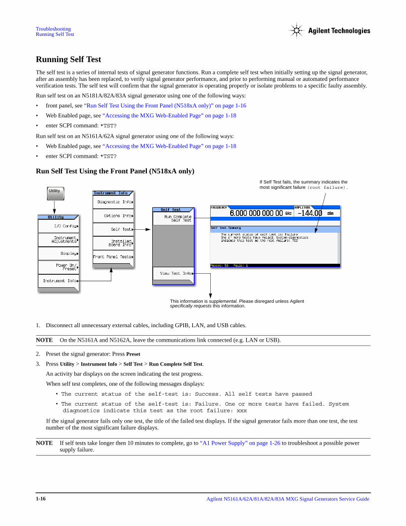
TroubleshootingRunning Self Test
Running Self Test
The self test is a series of internal tests of signal generator functions. Run a complete self test when initially setting up the signal generator, after an assembly has been replaced, to verify signal generator performance, and prior to performing manual or automated performance verification tests. The self test will confirm that the signal generator is operating properly or isolate problems to a specific faulty assembly.
Run self test on an N5181A/82A/83A signal generator using one of the following ways:
• front panel, see “Run Self Test Using the Front Panel (N518xA only)” on page 1-16
• Web Enabled page, see “Accessing the MXG Web-Enabled Page” on page 1-18
• enter SCPI command: *TST?
Run self test on an N5161A/62A signal generator using one of the following ways:
• Web Enabled page, see “Accessing the MXG Web-Enabled Page” on page 1-18
• enter SCPI command: *TST?
Run Self Test Using the Front Panel (N518xA only)
1. Disconnect all unnecessary external cables, including GPIB, LAN, and USB cables.
NOTE On the N5161A and N5162A, leave the communications link connected (e.g. LAN or USB).
2. Preset the signal generator: Press Preset
3. Press Utility > Instrument Info > Self Test > Run Complete Self Test.
An activity bar displays on the screen indicating the test progress.
When self test completes, one of the following messages displays:
• The current status of the self-test is: Success. All self tests have passed
• The current status of the self-test is: Failure. One or more tests have failed. System diagnostics indicate this test as the root failure: xxx
If the signal generator fails only one test, the title of the failed test displays. If the signal generator fails more than one test, the test number of the most significant failure displays.
NOTE If self tests take longer then 10 minutes to complete, go to “A1 Power Supply” on page 1-26 to troubleshoot a possible power supply failure.
If Self Test fails, the summary indicates the most significant failure (root failure).
This information is supplemental. Please disregard unless Agilent specifically requests this information.
Agilent N5161A/62A/81A/82A/83A MXG Signal Generators Service Guide 1-16

Troubleshooting Running Self Test
4. Locate the number and name of the failed test for your signal generator model in Table 1-1. The Resolution column in the table lists the assembly in which the failure is likely to have occurred or other troubleshooting information for that test.
5. Prior to permanently replacing any of the following assemblies:
• A2 Vector Module Assembly (N5162A/82A only)
• A7 Micro-Deck Assembly (N5183A only)
CAUTION The following process should only be completed if the suspect assembly has been confirmed to be bad/faulty. Completing the assembly replacement process accidently on a good/working CPU board could cause problems with the subsequent replacement of the A3 RF Assembly that turns out to be the actual bad/faulty board in the instrument.
Refer to “Assembly Installation and Removal Overview” on page 4-2, and complete the “Assembly Removal and Installation Procedure” on page 4-3.
Table 1-1 Self Tests
Self Test Failure Number Resolution
100 Digital Self Tests
101 & 102 Replace the A3 RF Assembly
103 Go to“A1 Power Supply” on page 1-26
104 Replace the A3 RF Assembly
200 Reference Self Tests
201 Go to“A1 Power Supply” on page 1-26
202 - 208 Replace the A3 RF Assembly
300 Synthesizer Self Tests
301 Go to“A1 Power Supply” on page 1-26
302 - 308 Replace the A3 RF Assembly
400 Output Self Tests
401 - 404 Replace the A3 RF Assembly
405 For N5161A/62A/81A/82A: Replace the A3 RF Assembly
For N5183A: Go to “Checking ALC Operation < 3.2 GHz (N5183A)” on page 1-48
406 - 412 Replace the A3 RF Assembly
500 Modulation Self Tests
501 Go to“A1 Power Supply” on page 1-26
502 - 506 Replace the A3 RF Assembly
507 For N5161A/62A/81A/82A: Replace the A3 RF Assembly
For N5183A: Go to “Amplitude Modulation Problems (N5183A)” on page 1-50
508 Pulse Mod For N5161A/62A/81A/82A: Replace the A3 RF Assembly
For N5183A: Go to “Pulse Modulation Problems (N5183A)” on page 1-51
600 Attenuator Self Tests
Agilent N5161A/62A/81A/82A/83A MXG Signal Generators Service Guide 1-17

TroubleshootingRunning Self Test
6. After permanently replacing one of the above listed assemblies ensure the “Assembly Removal and Installation Procedure” on page 4-3 has been completed.
CAUTION After replacing one of the assemblies listed above, the “Assembly Removal and Installation Procedure” on page 4-3 must be performed. If the “Assembly Removal and Installation Procedure” is not performed the instrument hardware may not function properly (e.g. instrument errors and possibly self-test failures).
Accessing the MXG Web-Enabled Page
NOTE LXI Class B Compliance Disclaimer
As of this product's firmware release in June 2008, LXI Class B Compliance Tests, using the new IEEE 1588-2008 Precision Time Protocol (PTP), were not available. This product provides the features of an LXI Class B instrument by adding LAN Triggering and Time Synchronization to its LXI Class C compliance. References to LXI Class B in the document and in the instrument menus and web pages do not insure LXI Class B compliance. This product will apply for LXI Class B Compliance when the LXI Consortium has approved its specification changes and can provide certified testing. For more information on the LXI standards, refer to http://www.lxistandard.org/home.
LXI-B is only available on instruments with serial prefixes >US/MY/SG4818.
NOTE The following example for accessing the MXG ATE instrument’s Web-Enabled uses the instrument’s predetermined default hostname that the MXG ATE ships with (e.g. a-<instrument model number>-<last 5 digits of the instrument serial number>).
The procedure that follows assumes the signal generator is running firmware A.01.20 or later.
MXG Web-Enabled SCPI command capability is not available for versions of Internet Explorer ≥7.0. (The SCPI Telnet softkey is inactive for these versions.) To use the Telnet SCPI, refer to Figure 1-3 on page 19.
601 - 603 Replace the A3 RF Assembly
700 BB Digital Self Tests
701 to 708 Replace the A2 Vector Module
800 BB Analog Baseband Self Tests
801 to 804 Replace the A2 Vector Module
900 BB RF Self Tests
901 to 905 Replace the A2 Vector Module
1100 MW ALC Self Tests
1101 -1104 Replace the A7 Micro Deck.
1105 Go to “Troubleshooting Self Test 1105” on page 1-25.
1106-1113 Replace the A7 Micro Deck.
1200 MW Multiplier Self Tests
1201 - 1205 Replace the A7 Micro Deck.
1300 MW Mod Filter Self Tests
1301 - 1304 Replace the A7 Micro Deck.
1400 MW Doubler Self Tests
1401 & 1402 Replace the A7 Micro Deck.
Table 1-1 Self Tests (Continued)
Self Test Failure Number Resolution
Agilent N5161A/62A/81A/82A/83A MXG Signal Generators Service Guide 1-18
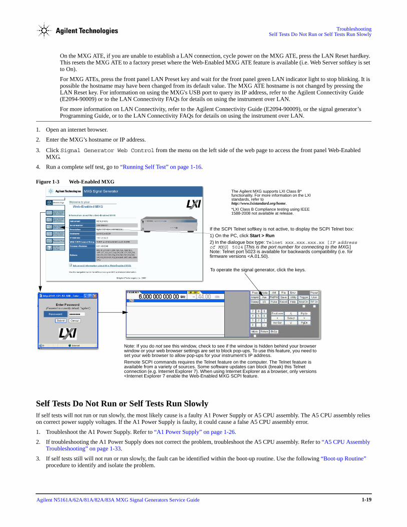
Troubleshooting Self Tests Do Not Run or Self Tests Run Slowly
On the MXG ATE, if you are unable to establish a LAN connection, cycle power on the MXG ATE, press the LAN Reset hardkey. This resets the MXG ATE to a factory preset where the Web-Enabled MXG ATE feature is available (i.e. Web Server softkey is set to On).
For MXG ATEs, press the front panel LAN Preset key and wait for the front panel green LAN indicator light to stop blinking. It is possible the hostname may have been changed from its default value. The MXG ATE hostname is not changed by pressing the LAN Reset key. For information on using the MXG's USB port to query its IP address, refer to the Agilent Connectivity Guide (E2094-90009) or to the LAN Connectivity FAQs for details on using the instrument over LAN.
For more information on LAN Connectivity, refer to the Agilent Connectivity Guide (E2094-90009), or the signal generator’s Programming Guide, or to the LAN Connectivity FAQs for details on using the instrument over LAN.
1. Open an internet browser.
2. Enter the MXG’s hostname or IP address.
3. Click Signal Generator Web Control from the menu on the left side of the web page to access the front panel Web-Enabled MXG.
4. Run a complete self test, go to “Running Self Test” on page 1-16.
Figure 1-3 Web-Enabled MXG
Self Tests Do Not Run or Self Tests Run SlowlyIf self tests will not run or run slowly, the most likely cause is a faulty A1 Power Supply or A5 CPU assembly. The A5 CPU assembly relies on correct power supply voltages. If the A1 Power Supply is faulty, it could cause a false A5 CPU assembly error.
1. Troubleshoot the A1 Power Supply. Refer to “A1 Power Supply” on page 1-26.
2. If troubleshooting the A1 Power Supply does not correct the problem, troubleshoot the A5 CPU assembly. Refer to “A5 CPU Assembly Troubleshooting” on page 1-33.
3. If self tests still will not run or run slowly, the fault can be identified within the boot-up routine. Use the following “Boot-up Routine” procedure to identify and isolate the problem.
Note: If you do not see this window, check to see if the window is hidden behind your browser window or your web browser settings are set to block pop-ups. To use this feature, you need to set your web browser to allow pop-ups for your instrument’s IP address.
Remote SCPI commands requires the Telnet feature on the computer. The Telnet feature is available from a variety of sources. Some software updates can block (break) this Telnet connection (e.g. Internet Explorer 7). When using Internet Explorer as a browser, only versions <Internet Explorer 7 enable the Web-Enabled MXG SCPI feature.
To operate the signal generator, click the keys.
The Agilent MXG supports LXI Class B* functionality. For more information on the LXI standards, refer to http://www.lxistandard.org/home.
*LXI Class B Compliance testing using IEEE 1588-2008 not available at release.
If the SCPI Telnet softkey is not active, to display the SCPI Telnet box:
1) On the PC, click Start > Run
2) In the dialogue box type: Telnet xxx.xxx.xxx.xx [IP address of MXG] 5024 [This is the port number for connecting to the MXG.] Note: Telnet port 5023 is available for backwards compatibility (i.e. for firmware versions <A.01.50).
Agilent N5161A/62A/81A/82A/83A MXG Signal Generators Service Guide 1-19

TroubleshootingBoot-up Routine
Boot-up RoutineIf you are unable to run a complete self test, monitor this boot-up routine to isolate a faulty assembly. The entire procedure must be completed prior to troubleshooting an identified faulty assembly. Complete each step, taking note of any item that does not respond as expected, then troubleshoot as described in step 18.
1. Check the yellow standby LED.
a. Connect the signal generator to a power source.
b. Turn the signal generator off.
c. Confirm that the yellow standby LED adjacent to the power button is lit.
2. Check the green LED.
a. Turn the signal generator on.
b. Confirm that the yellow standby LED is off.
c. Confirm that the green LED adjacent to the power button is lit.
3. Verify that the front panel LCD display turns on. (N5181A/82A/83A only)
4. Turn the signal generator off.
5. Remove the outer and inner instrument covers. Refer to Chapter 3, "Assembly Replacement" for instructions on removing the instrument covers.
6. Turn the signal generator on.
7. Visually inspect the fans to verify that the fans are turning.
8. Turn power off.
9. Position the signal generator with the bottom facing up.
10. Use Figure 1-4 to locate the yellow debug LEDs (TP1 through TP5).
Agilent N5161A/62A/81A/82A/83A MXG Signal Generators Service Guide 1-20
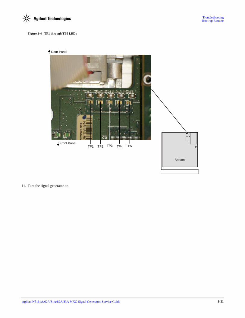
Troubleshooting Boot-up Routine
Figure 1-4 TP1 through TP5 LEDs
11. Turn the signal generator on.
TP1 TP2 TP3 TP4 TP5
Rear Panel
Front Panel
Agilent N5161A/62A/81A/82A/83A MXG Signal Generators Service Guide 1-21
TroubleshootingBoot-up Routine
12. Verify that the yellow debug LEDs complete the following start up routine.
1. All five LEDs are lit.
2. LED TP1, TP3, and TP4 are lit.
3. All five LEDs flicker.
4. All five LEDs turn off (boot-up complete).
13. Check the front panel display for start up errors.
14. Using Figure 1-5, verify that the following power supply voltage LEDs are on.
• +3.3VDF, DS1
• +5VDF, DS2
• +5.1VSBF, DS3
• +12VDF, DS4
• +32VAF, DS5
• +5VAF, DS6
• +9VAF, DS7
• +15VAF, DS8
• -7VAF, DS9
• -15VAF, DS10
Agilent N5161A/62A/81A/82A/83A MXG Signal Generators Service Guide 1-22

Troubleshooting Boot-up Routine
Figure 1-5 Power Supply LEDs
Front Panel
Rear Panel
Front Panel
Front Panel
Rear Panel
DS8
DS3DS1Rear Panel
DS2
DS4
DS9 DS7 DS6
DS10 DS5
Agilent N5161A/62A/81A/82A/83A MXG Signal Generators Service Guide 1-23

TroubleshootingBoot-up Routine
15. Using Figure 1-6, verify that the following red FPGA LEDs are off.
• Bridge FPGA and Programming PROM, DS100
• Analog Interface FPGA, DS200
• Synthesizer/Frac-N Controller FPGA, DS300
Figure 1-6 Red FPGA LEDs
16. Using Figure 1-6, verify that the following Unlock LEDs are off.
• Red USB Unlock, DS12
• Red ILB Unlock, DS13
• Yellow Reset, DS14
17. Using Figure 1-6, verify that the yellow DS11 LED is “blinking”. This LED indicates ongoing communication between the A5 CPU assembly and the A3 RF assembly.
DS100
DS300
DS200
Front Panel
Rear Panel Rear Panel
Rear Panel
Front Panel
Front Panel
DS12 DS13
DS14
DS11
Agilent N5161A/62A/81A/82A/83A MXG Signal Generators Service Guide 1-24

Troubleshooting Troubleshooting Self Test 1105
18. Troubleshoot all items that did not function as expected.
• May require firmware to be downloaded into instrument so FPGA code is correct.
CAUTION Not upgrading the firmware to the current version could cause errors during instrument boot-up.
• Only perform option Backup if CPU has been verified as the fault, else ignore error 617 Config error at this time.
• If the front panel yellow standby LED is not functioning, go to “The Green Front Panel Power Switch LED or Yellow Standby LED is Not Working” on page 1-57 to troubleshoot the error.
• If the front panel green power switch LED is not functioning, go to “The Green Front Panel Power Switch LED or Yellow Standby LED is Not Working” on page 1-57 to troubleshoot the error.
• If the front panel LCD display does not turn on, go to “LCD Display Appears to be Inoperative (Dark)” on page 1-52 to troubleshoot the error.
• If the fans do not turn on, go to “The Fans are Not Working” on page 1-64 to troubleshoot the error.
• If any of the yellow debug LEDs, TP1 through TP5, remain on, replace the A5 CPU assembly.
• If any of the power supply voltage LEDs are off, go to “A1 Power Supply” on page 1-26 to troubleshoot the error.
• If any of the FPGA LEDs are on, the signal generator has malfunctioned. Due to the design of the A3 RF and A5 CPU assemblies, the failure of one can interfere with the functionality of the other. Replace the A5 CPU assembly.
— If all FPGA LEDs turn off, then the A5 CPU was the faulty assembly.
— If the any of the FPGA LEDs remain on, the A3 RF assembly is at fault and needs to be replaced.
• If any of the Unlock LEDs are on, replace the A3 RF assembly.
• If the yellow DS11 LED is not “blinking”, the most likely assembly at fault is the A3 RF assembly. Go to “A5 CPU Assembly Troubleshooting” on page 1-33 to confirm that the A3 RF assembly is at fault.
19. After all boot-up routine errors have been successfully fixed, run a complete self test again.
Press: Utility > Instrument Info > Self Test > Run Complete Self Test.
Troubleshooting Self Test 1105A self test 1105 failure can be caused by the A3 RF assembly or the A7 Micro Deck. The following procedure will help identify the defective assembly.
1. After running a complete self test, where self test 1105 failed, press View Test Info.
2. Scroll to self test 1304.
3. Press View Details.
a. If multiple lower level 1304 self tests failed, replace the A3 RF assembly.
b. If only 1304 lower level self test 3.199 GHz Delta H/LB Detector failed, continue to step 4.
4. Disconnect W12 from the A3 RF assembly.
5. Connect the signal generator’s RF output through a 10 dB attenuator to a spectrum analyzer.
6. Set up the spectrum analyzer:
a. Press Preset.
b. Set the reference level to +30 dBm.
c. Set the CW frequency to 100 MHz.
d. Set the span to 100 MHz.
7. Set up the signal generator:
a. Press Preset.
b. Set the CW frequency to 100 MHz.
c. Press RF On/Off to On.
d. Press AMPTD > +10 dBm.
Agilent N5161A/62A/81A/82A/83A MXG Signal Generators Service Guide 1-25
TroubleshootingTroubleshooting Assembly Level Problems
e. Press AMPTD > ALC On.
8. Account for the attenuated output signal from the generator. The spectrum analyzer should be displaying a CW signal with an amplitude of > 18 dBm.
a. If the signal generators’s output level is < +18dBm, replace the A3 RF Assembly.
b. If the signal generator’s output level is > +18dBm, continue to step 9.
9. Repeat steps 6 through 8, but change the spectrum analyzer and signal generator’s frequencies to 1GHz, 2.5 GHz, and 3.199 GHz
• If the power level is good at all frequencies, replace the A7 Micro Deck.
• If the power level is not good at all frequencies, replace the A3 RF Deck.
NOTE At 3.2 GHz the signal generator’s CW signal will not be present.
Troubleshooting Assembly Level Problems
WARNING To allow the power supplies to discharge, wait 30 seconds after unplugging the instrument before removing or installing any assemblies.
CAUTION Before removing any instrument assembly, the instrument’s static and dynamic arrays must be configured for the exchange of assemblies. The process to do the appropriate configuration is performed automatically by the MXG with the Assembly Installation and Removal Overview front panel softkeys. Refer to the Assembly Installation and Removal Overview and to the “Hardware Assembly Installation and Removal Softkeys” on page 4-2.
A1 Power Supply
The A1 Power Supply is a switching supply with a switching frequency of 120 kHz. It operates from 88 RMS Vac to 269 Vac, at line frequencies of 45 Hz to approximately 400 Hz. The A1 Power Supply is designed with an automatic line-voltage and frequency selection. Except for the 5.1V standby, all power supply outputs are over-current protected and will not be damaged by a continuous short circuit.
1. Remove the outer and inner instrument covers. Refer to Chapter 3, "Assembly Replacement" for instructions on removing the instrument covers.
2. Reconnect the power cord.
3. Position the signal generator so the A3 RF assembly faces up.
4. Measure the voltage levels at A3J10.
Refer to Table 1-2 to determine the correct supply voltages for the signal generator’s power supplies. Because the power supply voltages are filtered or regulated on the A3 RF assembly, the faulty assembly could be either the A1 Power Supply or the A3 RF assembly.
5. If any voltage is incorrect, replace the A1 Power Supply.
NOTE If all A3J10 voltages are 0, the most likely cause is the internal power line fuse in the A1 Power Supply. The internal power line fuse is NOT replaceable on its own. The whole A1 Power Supply must be replaced.
6. Re-measure the voltage levels at A3J10.
7. If the voltages are still incorrect, the faulty assembly is the A3 RF assembly and not the A1 Power Supply. Replace the A3 RF assembly. If you replaced the A1 Power Supply, but the A3 RF assembly was the faulty assembly, you can return the new A1 Power Supply to Agilent.
Agilent N5161A/62A/81A/82A/83A MXG Signal Generators Service Guide 1-26

Troubleshooting Troubleshooting Assembly Level Problems
Figure 1-7 A3J10
FA
1
24
Front Panel
Rear Panel
Agilent N5161A/62A/81A/82A/83A MXG Signal Generators Service Guide 1-27

TroubleshootingTroubleshooting Assembly Level Problems
Table 1-2 A3J10 Output Connector Pin Assignment
A B C D E F
1 -15V (Aa)
aA= voltages or common ground to analog circuitry.
-15V (A) -15V (A) -15V (A) ACOM +32V (A)
2 ACOM ACOM ACOM ACOM ACOM ACOM
3 +15V (A) +15V (A) +15V (A) +15V (A) +15V (A) +15V (A)
4 ACOM ACOM ACOM ACOM ACOM ACOM
5 +5.2V (A) +5.2V (A) +5.2V (A) +5.2V (A) +5.2V (A) +5.2V (A)
6 +5.2V (A) +5.2V (A) +5.2V (A) +5.2V (A) +5.2V (A) +5.2V (A)
7 ACOM ACOM ACOM ACOM ACOM ACOM
8 ACOM ACOM ACOM ACOM ACOM ACOM
9 +9V (A) +9V (A) +9V (A) +9V (A) +9V (A) +9V (A)
10 +9V (A) +9V (A) +9V (A) +9V (A) +9V (A) +9V (A)
11 ACOM ACOM ACOM ACOM ACOM ACOM
12 ACOM ACOM ACOM ACOM ACOM ACOM
13 -7V (A) -7V (A) -7V (A) -7V (A) -7V (A) -7V (A)
14 ACOM ACOM ACOM ACOM ACOM ACOM
15 DbCOM
bD= voltages or common ground to digital circuitry,
DCOM DCOM DCOM DCOM DCOM
16 N.C +12V (D) +12V (D) +12V (D) +12V (D) +12V (D)
17 DCOM DCOM DCOM DCOM DCOM DCOM
18 +5.1V (D) +5.1V (D) +5.1V (D) +5.1V (D) +5.1V (D) +5.1V (D)
19 DCOM DCOM DCOM DCOM DCOM DCOM
20 DCOM DCOM DCOM DCOM DCOM DCOM
21 +3.35V (D) +3.35V (D) +3.35V (D) +3.35V (D) +3.35V (D) +3.35V (D)
22 +3.35V (D) +3.35V (D) +3.35V (D) +3.35V (D) +3.35V (D) +3.35V (D)
23 FAN_P FAN_P FAN_N FAN_N PS_TEMP +5.1
24 N.C OFFn TEMP_SENSE PS_FAULTn PWR_OK PS_ONn
Agilent N5161A/62A/81A/82A/83A MXG Signal Generators Service Guide 1-28
Troubleshooting Troubleshooting Assembly Level Problems
A2 Vector Module Troubleshooting (N5162A/82A Only)
The A2 Vector Module supports digital modulation in the N5162A/82A. The A2 Vector Module is a self contained, fully enclosed baseband generator assembly. There are no external test points or adjustments available. Troubleshooting the A2 Vector Module relies on the ability of the signal generator to complete the associated self tests.
1. Remove the outer and inner instrument covers. Refer to Chapter 3, "Assembly Replacement" for instructions on removing the instrument covers.
2. Reconnect the power cord.
3. Turn the signal generator on.
4. Using Figure 1-8, verify DS1 through DS6 on the A2 Vector Module run through the following initializing boot-up routine:
• DS1, DS2, DS3 and DS4 should blink briefly and then turn off.
• DS2 should blink continuously.
• DS5 should turn on and stay on until boot-up has completed, then it should blink continuously.
• DS6 LED should initially be off, then turn on and stay on as the assembly initialization is completed; DS5 begins blinking.
— If any LED does not act as expected, either the A2 Vector Module or the A5 CPU assembly is faulty. Use the following table to determine which assembly you need to troubleshoot or replace.
Table 1-3
LED Meaning Troubleshooting Indication
DS2 Heartbeat LED - driven by Interface FPGA from A5 CPU PCI Clock.
If the LED is not flashing the Interface FPGA is mis-configured. The A2 Vector Module may be faulty. Go to “A5 CPU Assembly Troubleshooting” on page 1-33 to confirm the A2 Vector Module is faulty.
DS3 Reset LED - driven by the Interface FPGA from power on reset circuit.
On = Failure. The A2 Vector Module may be faulty. Go to “A5 CPU Assembly Troubleshooting” on page 1-33 to confirm the A2 Vector Module is faulty.
DS4 Interface/Debug LED - driven by the Interface FPGA. On = Failure. The A2 Vector Module may be faulty. Go to “A5 CPU Assembly Troubleshooting” on page 1-33 to confirm the A2 Vector Module is faulty.
DS5 125 MHz Clock LED - driven by ARB FPGA from the 125 MHz DAC clock.
If the LED is not flashing or flashing at the wrong rate (2 Hz), replace the A2 Vector Module.
DS6 Firmware LED - driven by ARB FPGA/Firmware. Turns on at the end of boot-up.
If the LED does not turn on but the signal generator completed the boot-up routine, replace the A2 Vector Module.
Agilent N5161A/62A/81A/82A/83A MXG Signal Generators Service Guide 1-29

TroubleshootingTroubleshooting Assembly Level Problems
Figure 1-8 LED DS1 through DS6
5. Run a complete self test.
Press: Utility > Instrument Info > Self Test > Run Complete Self Test
• If any self test fails, refer to step 4 of “Running Self Test”.
DS2DS1 DS3 DS4
DS5
DS6
Front Panel
Rear Panel
Agilent N5161A/62A/81A/82A/83A MXG Signal Generators Service Guide 1-30

Troubleshooting Troubleshooting Assembly Level Problems
A3 RF Assembly Troubleshooting
The self test routine is specifically designed to troubleshoot the A3 RF assembly. Troubleshooting the A3 RF assembly relies on the ability of the signal generator to complete the associated self test.
1. Run a complete self test or A3 RF assembly specific self tests.
Press: Utility > Instrument Info > Self Test > Run Complete Self Test
• If any self test fails, refer to step 4 of “Running Self Test”.
2. If a complete self test cannot be run, monitor and troubleshoot the “Boot-up Routine” on page 1-20.
Agilent N5161A/62A/81A/82A/83A MXG Signal Generators Service Guide 1-31

TroubleshootingTroubleshooting Assembly Level Problems
A4 Internal Memory Card Troubleshooting (N5162A/82A Only)
NOTE Except in the signal generator’s ability to store and recall large quantities/sizes of files, the A4 Internal Memory Card alone will not affect the functionality of the signal generator.
The A4 Internal Memory Card contains a minimum of 800 MSamples (4 GB)1 of non-volatile user memory. User waveform lists and settings are maintained in the A4 Internal Memory Card.
When the signal generator is turned on, the A4 Internal Memory Card will run a mini-system check routine. During the mini-system check, LED D2 will blink, followed by three 2 Hz bursts. At the completion of the mini system check LED D2 will continue to blink slowly while in an idle state and will blink fast when the A4 Internal Memory Card is accessed, in response to the data transfer.
• If during the mini-system check, the signal generator reports system memory error “-310 System error: Expected memory media not found. Internal User storage”:
1. Verify the front panel USB port operates properly. Refer to “No Front Panel USB Activity” on page 1-64.
— If the front panel USB functions properly, replace the A4 Internal Memory Card.
— If the front panel USB does not function properly, replace the A3 RF assembly.
2. Attempt to access the A4 Internal Memory Card to recall or save a user file.
— If you cannot access the A4 Internal Memory Card, replace it.
3. Refer to Figure 1-9. Verify LED D2 is blinking when data is being transferred.
— If LED D2 is not blinking when data is being transferred, replace the A4 Internal Memory Card.
Figure 1-9 LED D2
1For serial numbers <MY4818xxxx, US4818xxxx, and SG4818xxxx, the persistent memory value = 512 MB (102 MSamples).
D2
Agilent N5161A/62A/81A/82A/83A MXG Signal Generators Service Guide 1-32

Troubleshooting Troubleshooting Assembly Level Problems
A5 CPU Assembly Troubleshooting
At power-on, the A5 CPU and the installed firmware run a series of initializing boot-up procedures and instrument operational checks. The operational checks are completed if all power supply voltages are present, the A5 CPU is working correctly and the main FPGA’s initialization has finished. If any part of the boot-up procedure fails, an error message will be displayed.
An A5 CPU failure symptom will change according to the type of failure that has occurred. A complete A5 CPU failure may still allow the signal generator to power up and all power supplies to be verified. Complete the following procedure to isolate the faulty assembly.
1. Monitor the “Boot-up Routine” on page 1-20.
• If any failures occur troubleshoot them.
2. If all power supplies are functional, attempt to communicate with the signal generator by:
• front panel
• LAN or USB. Refer to the Agilent Signal Generators Programming Guide, part number N5180-90005, for instructions on connecting through LAN and USB.
3. If minimal or no communication/functionality occurs, replace the A5 CPU.
4. If you can communicate, re-install the signal generator’s firmware. Go to www.agilent.com/find/upgradeassistant for information on re-installing the firmware.
NOTE Agilent recommends always loading the most recent version of firmware before replacing any assembly.
5. If any of the following occurs:
• No command response is received.
• “Request Timed Out” response is received.
• Firmware cannot be re-loaded and/or does not correct the symptom.
On the N5161A/62A:
CAUTION Read all of the following steps before beginning the procedure. Not following the procedure, can result in instrument errors and misdiagnosis of the faulty/bad part.
a. Put the instrument into diagnostics mode:
Power up the instrument while holding the LAN Reset hardkey.
The three front panel LEDs begin flashing simultaneously.
b. Press the LAN Reset hardkey once.
The ERROR LED should be flashing, but the LAN and 1588 LEDs should be dark/off.
The instrument is now in the “Recover from failed firmware update” mode. Refer to Table 1-9, “Diagnostics Mode (N5161A/62A),” on page 63.
If the ERROR LED is not flashing, and the LAN and 1588 LEDs are not dark/off then continue to press the LAN Reset hardkey until the correct pattern is being displayed.
CAUTION Cycling power on the instrument prior to selecting the correct pattern of LEDs could leave the instrument in an undesired diagnostic service mode.
If the power is accidently cycled on the instrument prior to having the correct LED pattern displayed (i.e. as described in this step) then repeat steps a and b.
c. Verify the instrument is connected to the LAN.
d. Load the most recent version of firmware.
If the instrument boots up without errors, proceed to step 7. If the firmware still cannot be loaded, proceed to step 6.
Agilent N5161A/62A/81A/82A/83A MXG Signal Generators Service Guide 1-33

TroubleshootingTroubleshooting Assembly Level Problems
On the N5181A/82A/83A:
a. Put the instrument into diagnostics mode:
Power up the instrument while holding the Preset hardkey.
The diagnostic service menu is displayed.
b. Press Continue > Next Page > Next Page > Bootup in no hardware mode [ ] (Verify an “x” is displayed in the “[ ]” (example: [x]))
The instrument is now in the “Bootup in no hardware mode”.
c. Verify the instrument is connected to the LAN.
d. Re-load the most recent version of firmware.
If the instrument boots up without errors, proceed to step 7. If the firmware still cannot be loaded, proceed to step 6.
6. If reloading the firmware does not correct the symptom, replace the A3 RF assembly.
7. After replacing the A3 RF assembly in a model N5183A instrument, go to Chapter 4, "Post-Repair Procedures and Performance Verification".
A6 DC-AC Inverter Interface Board (N5181A/82A/83A)
The A6 DC-AC Inverter Interface Board controls the Cold Cathode Fluorescent Tube (CCFT) backlight on the LCD Display module and converts a dc voltage to an ac voltage. Varying the dc voltage on the inverter will alter the backlight brightness. To determine if the A6 DC-AC Inverter Interface Board is the faulty assembly, complete the following procedure.
1. Turn the signal generator off.
2. Remove the front panel. Refer to Chapter 3, "Assembly Replacement".
3. Position the signal generator with the A3 RF assembly facing up.
4. Re-connect the W1 ribbon cable to the A3 RF assembly.
5. Use Figure 1-24 on page 57 to locate line switch S1. Press line switch S1 to turn the signal generator on.
6. Verify that the PIC processor is on:
• LED DS1, refer to Figure 1-10, should blink at a rate of 2 Hz. When DS1 is blinking the PIC processor has initialized and is operational.
Figure 1-10 LED DS1 and A6J5-1
DS1 A6J5-1
A6J1-3 A6J1-4
Agilent N5161A/62A/81A/82A/83A MXG Signal Generators Service Guide 1-34

Troubleshooting Troubleshooting Assembly Level Problems
7. Refer to Figure 1-10. Use a voltmeter with a small probe to measure A6J5-1; it should be ∼12V.
• If A6J5-1 is ∼12V:
— Measure the connections in Table 1-4.
— If the voltages are not present, replace the A6 DC-AC Inverter Interface Board.
— If the voltages are present, replace the LCD Display assembly.
• If A6J5-1 is not ∼12V, measure A6J1-3 or A6J1-4.
— If J1-3 or J1-4 is ∼12V, replace the A6 DC-AC Inverter Interface and LCD assemblies.
— If J1-3 or J1-4 is not ∼12V, go to step 8.
8. Refer to Figure 1-11. Using the voltmeter measure A3J6-3.
• If A3J6-3 is ∼12V replace the W1 ribbon cable.
• If A3J6-3 is not ∼12V go to step 9.
Figure 1-11 A3J6-3 and A3J10-B16
Table 1-4
Connector Voltage
J5-3 +11V
J5-4 (pwm_pic) >+1.3V
A3J6-3
A3J10-B16
Front Panel
Rear Panel
Rear Panel
Front Panel
Agilent N5161A/62A/81A/82A/83A MXG Signal Generators Service Guide 1-35

TroubleshootingTroubleshooting Assembly Level Problems
9. Refer to Figure 1-11. Using the voltmeter, measure A3J10-B16.
• If A3J10-B16 is ∼12V, perform the following steps:
a. Replace the A3 RF assembly.
b. Go to Chapter 4, "Post-Repair Procedures and Performance Verification".
• If A3J10-B16 is not ∼12V, replace the A1 Power Supply.
A7 Micro Deck (N5183A)• LEDs on page 1-36
• Power Supplies on page 1-37
LEDs
This procedure uses the LEDs on the A7 Micro Deck (Figure 1-12) for troubleshooting.
Figure 1-12Micro Deck LEDs
1. Remove the external cover and the top inside cover. Refer to Chapter 3, "Assembly Replacement" for instructions on removing the instrument covers.
2. Turn the signal generator on.
3. Observe the LEDs shown in Figure 1-12.
• DS1 (green) LED normal operation: blinks twice, then pauses and repeats.
a. If normal operation is not present, check LED DS7.
b. If DS7 is on, check DS7 as described below.
• DS2 to DS5 (amber) LEDs have no significance in troubleshooting the instrument.
• DS6 (red) LED is normally off. If DS6 is on, it indicates FPGA code is missing.
— Reload the firmware.
• DS7 (red) LED is normally off. When DS7 is on, it indicates a missing PCI clock.
a. Check J1-F24 (see Figure 1-13 on page 37 for test point locations) for a sine wave (>3 Vp–p at ∼32 MHz, period ∼31 ns).
b. If the signal is < 3 Vp–p:
1. Replace the A3 RF assembly.
2. Go to Chapter 4, "Post-Repair Procedures and Performance Verification".
DS7
DS2DS3DS4DS5DS1
DS6
Agilent N5161A/62A/81A/82A/83A MXG Signal Generators Service Guide 1-36

Troubleshooting Troubleshooting Assembly Level Problems
c. If the signal is > 3 Vp–p:
1. Replace the A7 Micro Deck.
2. Go to Chapter 4, "Post-Repair Procedures and Performance Verification".
Power Supplies
The A3 RF assembly provides the voltages shown in Table 1-5 to the corresponding pins on the ALC J1 connector on the A7 Micro Deck.
1. Measure the voltages on the A7 Micro Deck ALC J1 connector pins shown in Table 1-5.
NOTE There is no “J1” label on this side of the circuit board.
Figure 1-13 ALC J1 connector pins
Table 1-5 A7 Micro Deck Voltages
Voltage ALC Connector/Pin
–15V ± 5% (analog bus) J1-C1
–7V ± 5% (analog bus) J1-C1/D1/E1/F1
+15V ± 5% (analog bus) J1-C2/C3
+5V ± 5% (analog bus) J1-D2/E2/D3
+9.5V ± 5% (analog bus) J1-F2/F3
+5V ± 5% (digital bus) J1-C5
+3.3V ± 5% (digital bus) J1-D5/E5/F5/D6/E6/F6
+12V ± 5% (digital bus) J1-C6/C7/D7/E7/F7
A B C D E F
24
1
Agilent N5161A/62A/81A/82A/83A MXG Signal Generators Service Guide 1-37

TroubleshootingTroubleshooting Assembly Level Problems
2. If the voltages are present on all of the ALC J1 pins as shown in Table 1-5 on page 37:
a. Replace the A7 Micro Deck.
b. Go to Chapter 4, "Post-Repair Procedures and Performance Verification".
3. If any of the A7 Micro Deck power supply voltages are missing, remove the A7 Micro Deck and measure the corresponding voltages on the A3 RF assembly connector.
• If voltages are not present on the A3 RF assembly connector:
a. measure the power supply voltages using Table 1-8 on page 55.
b. Go to step 8 of The Signal Generator Does Not Power On on page 1-54.
• If the voltages are present:
a. Replace the A7 Micro Deck.
b. Go to Chapter 4, "Post-Repair Procedures and Performance Verification".
A8 Floating BNC Bypass Troubleshooting (N5183A)
The intent of the A8 Floating BNC Bypass assembly is to isolate ALC circuitry ground, chassis ground, and external equipment ground from each other. Diodes are used to shunt DC current and capacitors to remove interference components to ground.
1. If the external ALC appears unstable or noisy, use a digital multimeter to verify the bypass board is functioning properly. Using the ohm setting on your digital multimeter, test the bypass board. There should be a minimum resistance, typically ~100 ohms, between the outside barrel of the BNC and the chassis ground.
• If the resistance is ~100 ohms the A8 assembly is good.
• If the resistance is not ~100 ohms, replace the A8 assembly.
A9 Interface Board Troubleshooting (N5161A/62A)
The A9 provides voltages for the front panel LEDs and the LAN Reset hardkey. To determine if the A9 Interface Board is the faulty assembly, complete the following procedure.
1. With the signal generator turned off, verify the yellow front panel standby LED is on.
• If the yellow standby LED is not on, go to “The Green Front Panel Power Switch LED or Yellow Standby LED is Not Working” on page 1-57, to troubleshoot it.
2. With the signal generator turned on, verify the green front panel LED is on
• If the green LED is not on, go to “The Green Front Panel Power Switch LED or Yellow Standby LED is Not Working” on page 1-57, to troubleshoot it.
3. Turn the signal generator off.
4. Remove the front panel. Refer to Chapter 3, "Assembly Replacement".
5. Position the signal generator with the A3 RF assembly facing up.
6. Re-connect the W1 ribbon cable to the A3 RF assembly.
7. Use Figure 1-24 on page 57 to locate line switch S1. Press line switch S1 to turn the signal generator on.
8. Refer to Figure 1-14. Use a voltmeter with a small probe to measure A9J2-4; it should be ∼12V.
• If A9J2-4 is ∼12V:
— Measure the connections in Table 1-6.
Table 1-6
Connector Voltage
J2-8 +3.3V
J2-12 +3.3V
J2-34 +5.0V
Agilent N5161A/62A/81A/82A/83A MXG Signal Generators Service Guide 1-38

Troubleshooting Troubleshooting Assembly Level Problems
— If the voltages are not present, replace the A9 Interface Board.
— If the voltages are present, proceed to step 9.
• If A9J2-4 is not ∼12V, measure A9J2-3.
— If J2-3 is ∼12V, replace the A9 Interface Board.
— If J2-3 is not ∼12V, go to step 9.
Figure 1-14 A9 Interface Board (A9J2-3 and A9J2-4 Test Points)
9. Refer to Figure 1-15. Using the voltmeter measure A3J6-4.
• If A3J6-4 is ∼12V replace the W1 ribbon cable.
• If A3J6-4 is not ∼12V go to step 10.
A9J2-3
A9J2-4
A9J2-34
Agilent N5161A/62A/81A/82A/83A MXG Signal Generators Service Guide 1-39

TroubleshootingNo Output Power or Output Power is Unleveled (N5183A)
Figure 1-15 A3J6-3 and A3J10-B16
10. Refer to Figure 1-15. Using the voltmeter, measure A3J10-B16.
• If A3J10-B16 is ∼12V, perform the following steps:
a. Replace the A3 RF assembly.
b. Go to Chapter 4, "Post-Repair Procedures and Performance Verification".
• If A3J10-B16 is not ∼12V, replace the A1 Power Supply.
No Output Power or Output Power is Unleveled (N5183A)1. Connect the signal generator’s RF output through a 10 dB attenuator to a spectrum analyzer.
2. Set up the spectrum analyzer:
a. Press Preset.
b. Set the reference level to +25 dBm.
c. Set the start frequency to 50 kHz.
d. Set the stop frequency to the signal generator’s maximum frequency.
e. Set trace to Max Hold.
3. Set up the signal generator:
a. Press Preset.
b. Press SWEEP > Sweep Type List Step to Step.
c. Press Configure Step Sweep.
• Press Freq Start > 100 > kHz.
• Press Freq Stop > <maximum_signal_generator_frequency> > GHz.
• Press # Points > 501 > Enter.
• Press More > Step Dwell > 2 > msec.
A3J6-4
A3J10-B16
Front Panel
Rear Panel
Rear Panel
Front Panel
Agilent N5161A/62A/81A/82A/83A MXG Signal Generators Service Guide 1-40

Troubleshooting No Output Power or Output Power is Unleveled (N5183A)
• Press Return > Return > Sweep > Freq Off On to On.
d. Press RF On/Off to On.
e. Press AMPTD > ALC Off On to Off.
f. Press AMPTD > <maximum settable power> > dBm.
4. Let the signal generator sweep until the spectrum analyzer displays a sufficient number of points to provide a good representation of power performance across the range of frequencies in the sweep.
5. Using the marker feature on the spectrum analyzer, measure the lowest power level displayed for sweep points between 100 kHz and the maximum signal generator frequency, and record the lowest power reading.
6. Press AMPTD > ALC Off On to On
7. Let the signal generator sweep until the spectrum analyzer displays a sufficient number of points to provide a good representation of power performance across the range of frequencies in the sweep.
8. Using the marker feature on the spectrum analyzer, measure the lowest power level displayed for sweep points between 100 kHz and the maximum signal generator frequency, and record the lowest power reading.
9. Compare the measured values from step 5 and step 8 with the values listed for maximum output power in the N5183A Data Sheet.
• If the measured power with the ALC off is less than the specified power shown in the N5183A Data Sheet, go to “Low Output Power or No Output Power < 3.2 GHz (N5183A)” on page 1-41 or “Low Output Power or No Output Power >= 3.2 GHz (N5183A)” on page 1-46.
• If the measured power with the ALC off is greater than or equal to the specified power shown in the N5183A Data Sheet, but is less than the specified power shown in the N5183A Data Sheet when the ALC is on, perform the following steps:
a. Replace the A7 Micro Deck.
b. Go to Chapter 4, "Post-Repair Procedures and Performance Verification".
Low Output Power or No Output Power < 3.2 GHz (N5183A)1. Connect the signal generator’s RF output through a 10 dB attenuator to a spectrum analyzer.
2. Set up the spectrum analyzer:
a. Press Preset.
b. Set the reference level to +25 dBm.
c. Set the start frequency to 50 kHz.
d. Set the stop frequency to 3.2 GHz.
e. Set Trace to Max Hold.
3. Set up the signal generator:
a. Press Preset.
b. Press SWEEP > Sweep Type List Step to Step.
c. Press Configure Step Sweep.
• Press Freq Start > 100 > kHz.
• Press Freq Stop > 3.1999 > GHz.
• Press # Points > 501 > Enter.
• Press More > Step Dwell > 2 > msec.
• Press Return > Return > Sweep > Freq Off On to On.
d. Press RF On/Off to On.
e. Press AMPTD > ALC Off On to Off.
f. Press AMPTD > <maximum settable power> > dBm.
4. Let the signal generator sweep until the spectrum analyzer displays a sufficient number of points to provide a good representation of power performance across the range of frequencies in the sweep.
5. Using the marker feature on the spectrum analyzer, measure the lowest power level displayed for sweep points between 100 kHz and 3.1999 GHz, and record the lowest power reading.
Agilent N5161A/62A/81A/82A/83A MXG Signal Generators Service Guide 1-41
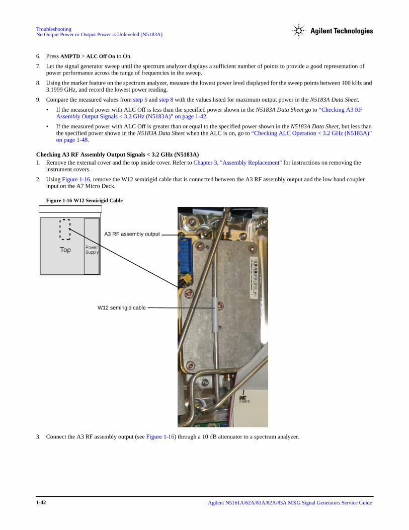
TroubleshootingNo Output Power or Output Power is Unleveled (N5183A)
6. Press AMPTD > ALC Off On to On.
7. Let the signal generator sweep until the spectrum analyzer displays a sufficient number of points to provide a good representation of power performance across the range of frequencies in the sweep.
8. Using the marker feature on the spectrum analyzer, measure the lowest power level displayed for the sweep points between 100 kHz and 3.1999 GHz, and record the lowest power reading.
9. Compare the measured values from step 5 and step 8 with the values listed for maximum output power in the N5183A Data Sheet.
• If the measured power with ALC Off is less than the specified power shown in the N5183A Data Sheet go to “Checking A3 RF Assembly Output Signals < 3.2 GHz (N5183A)” on page 1-42.
• If the measured power with ALC Off is greater than or equal to the specified power shown in the N5183A Data Sheet, but less than the specified power shown in the N5183A Data Sheet when the ALC is on, go to “Checking ALC Operation < 3.2 GHz (N5183A)” on page 1-48.
Checking A3 RF Assembly Output Signals < 3.2 GHz (N5183A)1. Remove the external cover and the top inside cover. Refer to Chapter 3, "Assembly Replacement" for instructions on removing the
instrument covers.
2. Using Figure 1-16, remove the W12 semirigid cable that is connected between the A3 RF assembly output and the low band coupler input on the A7 Micro Deck.
Figure 1-16 W12 Semirigid Cable
3. Connect the A3 RF assembly output (see Figure 1-16) through a 10 dB attenuator to a spectrum analyzer.
W12 semirigid cable
A3 RF assembly output
Agilent N5161A/62A/81A/82A/83A MXG Signal Generators Service Guide 1-42

Troubleshooting No Output Power or Output Power is Unleveled (N5183A)
4. Set up the spectrum analyzer:
a. Press Preset.
b. Set the reference level to +25 dBm (or maximum available power).
c. Set the start frequency to 50 kHz.
d. Set the stop frequency to 3.2 GHz.
e. Set Trace to Max Hold.
5. Set up the signal generator:
a. Press Preset.
b. Press SWEEP > Sweep Type List Step to Step.
c. Press Configure Step Sweep.
• Press Freq Start > 100 > kHz.
• Press Freq Stop > 3.1999 > GHz.
• Press # Points > 501 > Enter.
• Press More > Step Dwell > 2 > msec.
• Press Return > Return > Sweep > Freq Off On to On.
d. Press RF On/Off to On.
e. Press AMPTD > ALC Off On to Off.
f. Press AMPTD > <maximum settable power> > dBm.
6. Let the signal generator sweep until the spectrum analyzer displays a sufficient number of points to provide a good representation of the power performance across the range of frequencies in the sweep.
7. Using the marker feature on the spectrum analyzer, measure the lowest power level displayed for sweep points between 100 kHz and 3.1999 GHz, and record the lowest power reading.
• If the measured power is < 23 dBm:
a. Replace the A3 RF assembly.
b. Go to Chapter 4, "Post-Repair Procedures and Performance Verification".
• If the measured power is ≥ 23 dBm and Option 1EM (RF output on the rear panel) is installed:
a. Replace the A7 Micro Deck.
b. Go to Chapter 4, "Post-Repair Procedures and Performance Verification".
• If the measured power is ≥ 23 dBm and the signal generator has the standard RF output (front panel output), continue to “Checking Attenuator Output Signals < 3.2 GHz (N5183A)” on page 1-44.
Agilent N5161A/62A/81A/82A/83A MXG Signal Generators Service Guide 1-43
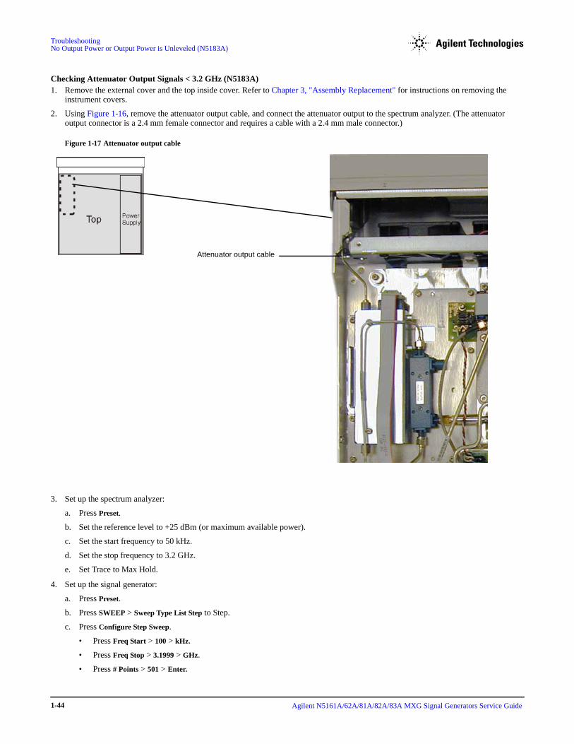
TroubleshootingNo Output Power or Output Power is Unleveled (N5183A)
Checking Attenuator Output Signals < 3.2 GHz (N5183A)1. Remove the external cover and the top inside cover. Refer to Chapter 3, "Assembly Replacement" for instructions on removing the
instrument covers.
2. Using Figure 1-16, remove the attenuator output cable, and connect the attenuator output to the spectrum analyzer. (The attenuator output connector is a 2.4 mm female connector and requires a cable with a 2.4 mm male connector.)
Figure 1-17 Attenuator output cable
3. Set up the spectrum analyzer:
a. Press Preset.
b. Set the reference level to +25 dBm (or maximum available power).
c. Set the start frequency to 50 kHz.
d. Set the stop frequency to 3.2 GHz.
e. Set Trace to Max Hold.
4. Set up the signal generator:
a. Press Preset.
b. Press SWEEP > Sweep Type List Step to Step.
c. Press Configure Step Sweep.
• Press Freq Start > 100 > kHz.
• Press Freq Stop > 3.1999 > GHz.
• Press # Points > 501 > Enter.
Attenuator output cable
Agilent N5161A/62A/81A/82A/83A MXG Signal Generators Service Guide 1-44

Troubleshooting No Output Power or Output Power is Unleveled (N5183A)
• Press More > Step Dwell > 2 > msec.
• Press Return > Return > Sweep > Freq Off On to On.
d. Press RF On/Off to On.
e. Press AMPTD > ALC Off On to Off.
f. Press AMPTD > <maximum settable power> > dBm.
5. Let the signal generator sweep until the spectrum analyzer displays a sufficient number of points to provide a good representation of the power performance across the range of frequencies in the sweep.
6. Using the marker feature on the spectrum analyzer, measure the lowest power level displayed for sweep points between 100 kHz and 3.1999 GHz, and record the lowest power reading.
7. Using the spectrum analyzer, measure the lowest power level at the attenuator output.
• If the lowest power level is less than the specified power shown in the maximum output power section of the N5183A Data Sheet:
a. Replace the A7 Micro Deck.
b. Go to Chapter 4, "Post-Repair Procedures and Performance Verification".
• If the lowest power level is greater than the specified power level shown in the maximum output power section of the N5183A Data Sheet:
a. Reconnect the cable to the attenuator.
b. Disconnect the cable from the RF output connector.
c. Check the loss through the cable.
d. If the cable is bad, replace the cable.
e. If the cable is good, reconnect the cable to the RF output connector.
f. Measure the loss through the RF output connector.
g. If the RF connector is bad, replace the connector.
h. If any parts are replaced, go to Chapter 4, "Post-Repair Procedures and Performance Verification".
Agilent N5161A/62A/81A/82A/83A MXG Signal Generators Service Guide 1-45

TroubleshootingNo Output Power or Output Power is Unleveled (N5183A)
Low Output Power or No Output Power >= 3.2 GHz (N5183A)1. Remove the external cover and the top inside cover. Refer to Chapter 3, "Assembly Replacement" for instructions on removing the
instrument covers.
2. Using Figure 1-18, remove the W13 semirigid cable between the A3 RF output assembly and the 20 GHz doubler input located on the A7 Micro Deck.
Figure 1-18 W13 Semirigid Cable
3. Connect the A3 RF assembly output (see Figure 1-18) through a 10 dB attenuator to a spectrum analyzer.
4. Set up the spectrum analyzer:
a. Press Preset.
b. Set the reference level to +10 dBm.
c. Set the start frequency to 2.3 GHz.
d. Set the stop frequency to 5.3 GHz.
e. Set Trace to Max Hold.
5. Set up the signal generator:
a. Press Preset.
b. Press SWEEP > Sweep Type List Step to Step.
c. Press Configure Step Sweep.
• Press Freq Start > 2.8 > GHz.
• Press Freq Stop > 10.4 > GHz.
• Press # Points > 501 > Enter.
• Press More > Step Dwell > 2 > msec.
• Press Return > Return > Sweep > Freq Off On to On.
d. Press RF On/Off to On.
e. Press AMPTD > <maximum settable power> > dBm.
f. Press AMPTD > ALC Off On to Off.
W13 semirigid cable
A3 RF assembly output
Agilent N5161A/62A/81A/82A/83A MXG Signal Generators Service Guide 1-46

Troubleshooting No Output Power or Output Power is Unleveled (N5183A)
6. Let the signal generator sweep until the spectrum analyzer displays a sufficient number of points to provide a good representation of the power performance across the range of frequencies in the sweep.
7. Using the marker feature on the spectrum analyzer, measure the lowest power level displayed for sweep points between 2.5 GHz and 5 GHz.
• If the measured power is < –5 dBm (for example, –6 dBm):
a. Replace the A3 RF assembly.
b. Go to Chapter 4, "Post-Repair Procedures and Performance Verification".
• If the measured power is ≥ –5 dBm (for example, –4 dBm), and the signal generator has Option 1EM (RF output on rear panel):
a. Replace the A7 Micro Deck.
b. Go to Chapter 4, "Post-Repair Procedures and Performance Verification".
• If the measured power is ≥ –5 dBm (for example, –4 dBm), and the signal generator has standard RF output (front output):
a. Turn off the signal generator and reinstall the W13 cable between the A3 RF assembly output and the 20 GHz doubler input.
b. Continue to Checking Attenuator Output Signals >= 3.2 GHz (N5183A).
Checking Attenuator Output Signals >= 3.2 GHz (N5183A)1. Remove the external cover and the top inside cover. Refer to Chapter 3, "Assembly Replacement" for instructions on removing the
instrument covers.
2. Using Figure 1-17 on page 44, remove the attenuator output cable and connect the attenuator output to the spectrum analyzer. (The attenuator output connector is a 2.4 mm female connector and requires a cable with a 2.4 mm male connector.)
3. Set up the spectrum analyzer:
a. Press Preset.
b. Set the reference level to +10 dBm.
c. Set the start frequency to 3.1GHz.
d. Set the stop frequency to the maximum source frequency.
e. Set Trace to Max Hold.
4. Set up the signal generator:
a. Press Preset.
b. Press SWEEP > Sweep Type List Step to Step.
c. Press Configure Step Sweep.
• Press Freq Start > 3.1 > GHz.
• Press Freq Stop > <maximum source frequency> > GHz.
• Press # Points > 501 > Enter.
• Press More > Step Dwell > 2 > msec.
• Press Return > Return > Sweep > Freq Off On to On.
d. Press RF On/Off to On.
5. Turn on the signal generator and set it as follows:
a. Press AMPTD > <maximum settable power> > dBm.
b. Press AMPTD > ALC Off On to Off.
Agilent N5161A/62A/81A/82A/83A MXG Signal Generators Service Guide 1-47
TroubleshootingChecking ALC Operation < 3.2 GHz (N5183A)
6. Using the spectrum analyzer, measure the lowest power level at the attenuator output.
• If the lowest power level is less than the specified power shown in the maximum output power section of the N5183A Data Sheet:
a. Replace the A7 Micro Deck.
b. Go to Chapter 4, "Post-Repair Procedures and Performance Verification".
• If the lowest power level is greater than the specified power level shown in the maximum output power section of the N5183A Data Sheet:
a. Reconnect the cable to the attenuator.
b. Disconnect the cable from the RF output connector.
c. Check the loss through the cable.
d. If the cable loss is >1dB, replace the cable.
e. If the cable is good, reconnect the cable to the RF output connector.
f. Measure the loss through the RF output connector.
g. If the RF connector loss is >2dB, replace the connector.
7. If any of the parts are replaced, go to Chapter 4, "Post-Repair Procedures and Performance Verification".
Checking ALC Operation < 3.2 GHz (N5183A)In this procedure you are looking for a pattern in the voltage change when you change the amplitude. For each change in amplitude, you should measure a change of approximately one volt, relative to the previous and subsequent voltage values. The Example Voltages column in Table 1-7 on page 1-49 demonstrates this change while also showing that it is not always exactly one volt.
1. Remove the external cover and the top inside cover. Refer to Chapter 3, "Assembly Replacement" for instructions on removing the instrument covers.
2. Set up the signal generator:
a. Press Preset.
b. Press FREQ > 2 > GHz.
c. Press RF On/Off to On.
d. Press AMPTD > ALC Off On to Off.
e. Press Atten/ALC Control > Atten Hold Off On to On.
f. Press Set Atten > 0 > dB.
g. Press AMPTD > 10 > dBm.
3. Using Figure 1-19, remove the W14 modulator drive cable from ALC LOB MOD (J15).
4. Measure the center pin voltage on the J15 connector using an oscilloscope.
Agilent N5161A/62A/81A/82A/83A MXG Signal Generators Service Guide 1-48
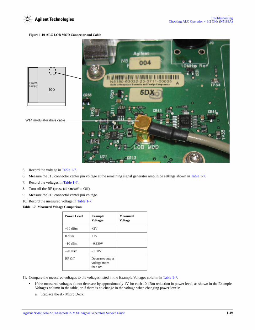
Troubleshooting Checking ALC Operation < 3.2 GHz (N5183A)
Figure 1-19 ALC LOB MOD Connector and Cable
5. Record the voltage in Table 1-7.
6. Measure the J15 connector center pin voltage at the remaining signal generator amplitude settings shown in Table 1-7.
7. Record the voltages in Table 1-7.
8. Turn off the RF (press RF On/Off to Off).
9. Measure the J15 connector center pin voltage.
10. Record the measured voltage in Table 1-7.
11. Compare the measured voltages to the voltages listed in the Example Voltages column in Table 1-7.
• If the measured voltages do not decrease by approximately 1V for each 10 dBm reduction in power level, as shown in the Example Voltages column in the table, or if there is no change in the voltage when changing power levels:
a. Replace the A7 Micro Deck.
Table 1-7 Measured Voltage Comparison
Power Level Example Voltages
Measured Voltage
+10 dBm +2V
0 dBm +1V
–10 dBm –0.130V
–20 dBm –1.30V
RF Off Decreases output voltage more than 8V
W14 modulator drive cable
Agilent N5161A/62A/81A/82A/83A MXG Signal Generators Service Guide 1-49

TroubleshootingAmplitude Modulation Problems (N5183A)
b. Go to Chapter 4, "Post-Repair Procedures and Performance Verification".
• If the measured voltages decrease by approximately 1V for each 10 dBm reduction in power level, as shown in the Example Voltages column in the table, verify the continuity of the W14 modulator drive cable (see Figure 1-19 on page 49) to the A3 RF assembly.
— If the cable is bad, replace the cable.
— If the cable is good, replace the RF assembly.
12. Go to Chapter 4, "Post-Repair Procedures and Performance Verification".
Amplitude Modulation Problems (N5183A)1. Remove the external cover and the top inside cover. Refer to Chapter 3, "Assembly Replacement" for instructions on removing the
instrument covers.
2. Set up the signal generator:
a. Press Preset.
b. Press FREQ > 5 > GHz.
c. Press RF On/Off to On.
d. Press AMPTD > 0 > dBm.
e. Press AM > AM Off On to On.
f. Press AM Type LIN EXP to EXP.
g. Press AM Depth > 40 > dB.
h. Press AM Rate > 400 > Hz.
Figure 1-20 ALC J1-E3
3. Using an oscilloscope, measure ALC J1-E3 (Figure 1-20).
NOTE There is no “J1” label on this side of the circuit board.
You should see a sine wave with an amplitude > 2.5 Vp–p and a period of 2.5 ms.
J1-E3
Agilent N5161A/62A/81A/82A/83A MXG Signal Generators Service Guide 1-50
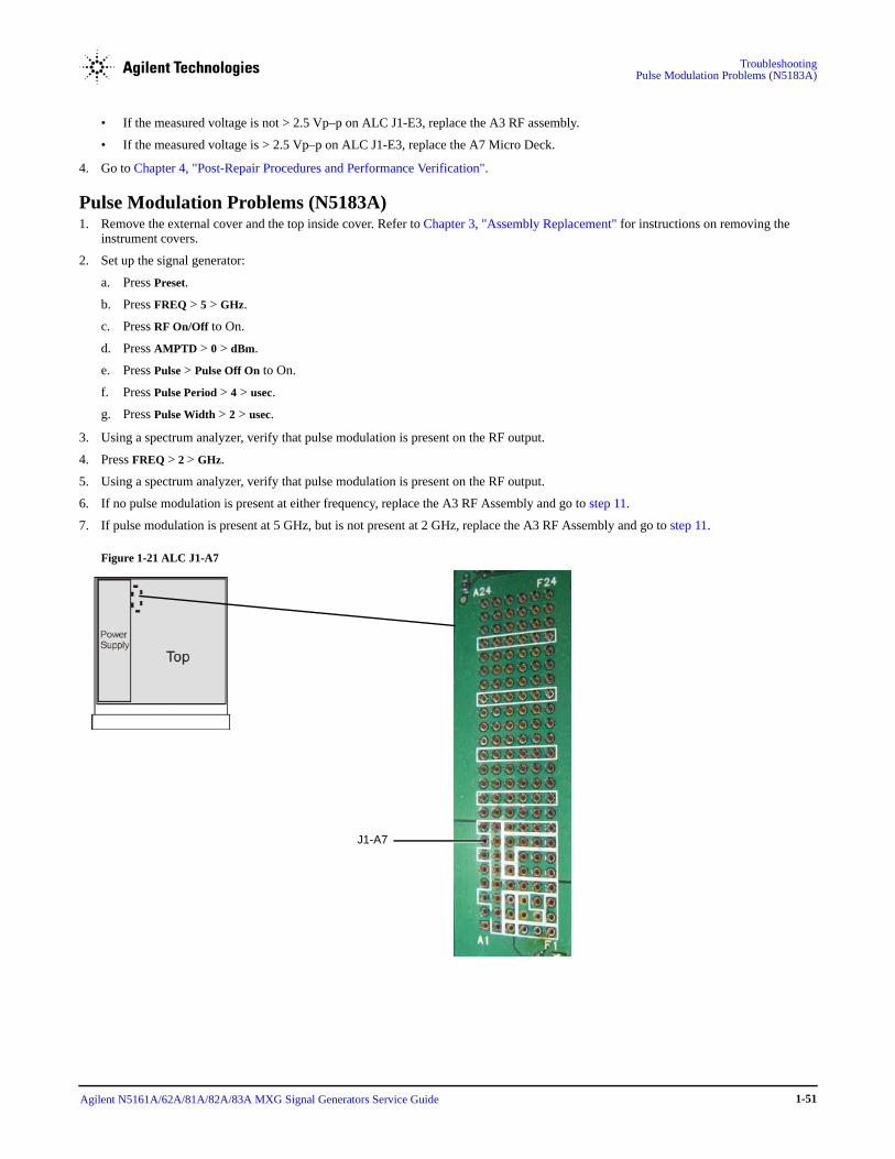
Troubleshooting Pulse Modulation Problems (N5183A)
• If the measured voltage is not > 2.5 Vp–p on ALC J1-E3, replace the A3 RF assembly.
• If the measured voltage is > 2.5 Vp–p on ALC J1-E3, replace the A7 Micro Deck.
4. Go to Chapter 4, "Post-Repair Procedures and Performance Verification".
Pulse Modulation Problems (N5183A)1. Remove the external cover and the top inside cover. Refer to Chapter 3, "Assembly Replacement" for instructions on removing the
instrument covers.
2. Set up the signal generator:
a. Press Preset.
b. Press FREQ > 5 > GHz.
c. Press RF On/Off to On.
d. Press AMPTD > 0 > dBm.
e. Press Pulse > Pulse Off On to On.
f. Press Pulse Period > 4 > usec.
g. Press Pulse Width > 2 > usec.
3. Using a spectrum analyzer, verify that pulse modulation is present on the RF output.
4. Press FREQ > 2 > GHz.
5. Using a spectrum analyzer, verify that pulse modulation is present on the RF output.
6. If no pulse modulation is present at either frequency, replace the A3 RF Assembly and go to step 11.
7. If pulse modulation is present at 5 GHz, but is not present at 2 GHz, replace the A3 RF Assembly and go to step 11.
Figure 1-21 ALC J1-A7
J1-A7
Agilent N5161A/62A/81A/82A/83A MXG Signal Generators Service Guide 1-51

TroubleshootingLCD Display Appears to be Inoperative (Dark)
8. If no pulse modulation is present at 5 GHz, but pulse modulation is present at 2 GHz, use an oscilloscope to measure ALC J1-A7. (Refer to Figure 1-21.)
NOTE There is no “J1” label on this side of the circuit board.
With Pulse on, a square wave should be present at J1-A7 with an amplitude > 3.2 Vp–p and a period of 4 μs.
9. If no pulse modulation is present on ALC J1-A7, replace the A7 Micro Deck.
10. If pulse modulation is present on ALC J1-A7 and occurs at < 3.2 GHz, but not at > 3.2 GHz, replace the A7 Micro Deck.
11. If any of the assemblies are replaced, go to Chapter 4, "Post-Repair Procedures and Performance Verification".
LCD Display Appears to be Inoperative (Dark)1. Verify that the display brightness and contrast are set properly.
• The display brightness can be adjusted from 0 (low brightness) to 100 (high brightness), using the RPG knob, arrow keys, or the numeric keypad.
• The display contrast can be adjusted from 35 (low contrast) to 55 (high contrast), using the RPG knob, arrow keys or the numeric keypad.
When both the display brightness and contrast are set to their minimums, the display may be too dark to see the softkeys. Try to adjust the brightness and contrast values. Press the following keys: Utility > the third softkey > the first softkey, and then turn the RPG knob to the right to increase the brightness. Then press: Utility > the third softkey > the second softkey and turn the RPG knob to the right to increase the contrast.
2. With the signal generator turned off, verify the yellow front panel standby LED is on.
• If the yellow standby LED is not on, go to “The Green Front Panel Power Switch LED or Yellow Standby LED is Not Working” on page 1-57, to troubleshoot it.
3. With the signal generator turned on, verify the green front panel LED is on
• If the green LED is not on, go to “The Green Front Panel Power Switch LED or Yellow Standby LED is Not Working” on page 1-57, to troubleshoot it.
4. Verify that the screen saver is not on.
• Press any front panel key to turn the screen saver off.
5. Verify, by listening, that the fans are on.
• If the fans are not on, go to “The Fans are Not Working” on page 1-64, to troubleshoot them.
6. Verify that the LEDs for the Mod On/Off and RF On/Off keys turn on and off when pressed.
7. If steps 1 through 6 do not fix the LCD Display issue, the most likely cause is a faulty A6 DC-AC Inverter Interface Board. Refer to “A6 DC-AC Inverter Interface Board (N5181A/82A/83A)” on page 1-34 to troubleshoot it.
The Signal Generator Does Not Power On1. Verify that the power cord and line voltages are correct. Refer to the N5161A, N5162A, N5181A, N5182A or N5183A Data Sheet.
2. With the signal generator turned off, verify that the yellow front panel standby LED is on.
• If the yellow standby LED is not on, go to “The Green Front Panel Power Switch LED or Yellow Standby LED is Not Working” on page 1-57, to troubleshoot it.
3. Remove the outer and inner instrument covers. Refer to Chapter 3, "Assembly Replacement" for instructions on removing the instrument covers.
4. Position the signal generator with the A3 RF assembly facing up.
5. Re-connect the power cord.
Agilent N5161A/62A/81A/82A/83A MXG Signal Generators Service Guide 1-52
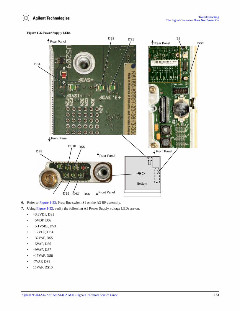
Troubleshooting The Signal Generator Does Not Power On
Figure 1-22 Power Supply LEDs
6. Refer to Figure 1-22. Press line switch S1 on the A3 RF assembly.
7. Using Figure 1-22, verify the following A1 Power Supply voltage LEDs are on.
• +3.3VDF, DS1
• +5VDF, DS2
• +5.1VSBF, DS3
• +12VDF, DS4
• +32VAF, DS5
• +5VAF, DS6
• +9VAF, DS7
• +15VAF, DS8
• -7VAF, DS9
• 15VAF, DS10
Front Panel
Rear Panel
Front Panel
Front Panel
Rear Panel
DS8
DS3DS1
Rear PanelDS2
DS4
DS9 DS7 DS6
DS10 DS5
S1
Agilent N5161A/62A/81A/82A/83A MXG Signal Generators Service Guide 1-53

TroubleshootingThe Signal Generator Does Not Power On
8. Using Table 1-8, if one or more power supply LEDs are not on or if the signal generator does not appear to have powered up correctly, use a voltmeter with a small probe to measure the power supply voltages on connector A3J10 (Figure 1-23).
• If any voltages are outside the listed values, the fault is likely with the A1 Power Supply. Replace the A1 Power Supply.
Figure 1-23 A3J10
FA
1
24
Front Panel
Rear Panel
Agilent N5161A/62A/81A/82A/83A MXG Signal Generators Service Guide 1-54
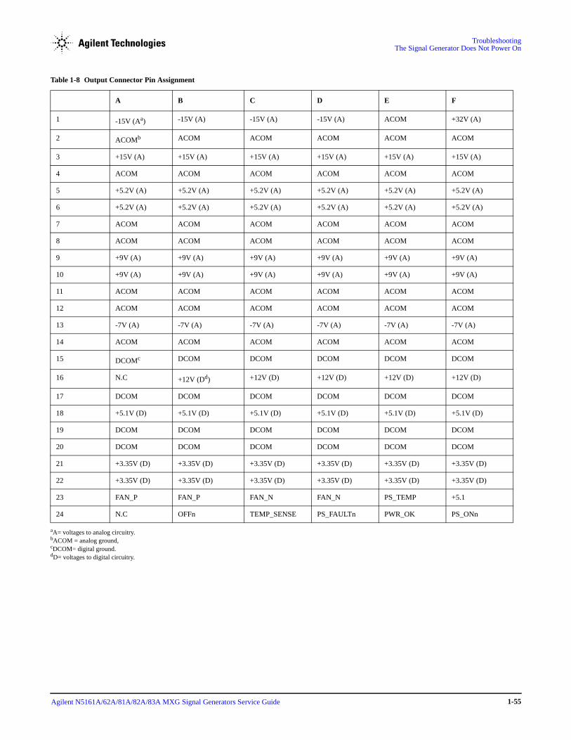
Troubleshooting The Signal Generator Does Not Power On
Table 1-8 Output Connector Pin Assignment
A B C D E F
1 -15V (Aa)
aA= voltages to analog circuitry.
-15V (A) -15V (A) -15V (A) ACOM +32V (A)
2 ACOMb
bACOM = analog ground,
ACOM ACOM ACOM ACOM ACOM
3 +15V (A) +15V (A) +15V (A) +15V (A) +15V (A) +15V (A)
4 ACOM ACOM ACOM ACOM ACOM ACOM
5 +5.2V (A) +5.2V (A) +5.2V (A) +5.2V (A) +5.2V (A) +5.2V (A)
6 +5.2V (A) +5.2V (A) +5.2V (A) +5.2V (A) +5.2V (A) +5.2V (A)
7 ACOM ACOM ACOM ACOM ACOM ACOM
8 ACOM ACOM ACOM ACOM ACOM ACOM
9 +9V (A) +9V (A) +9V (A) +9V (A) +9V (A) +9V (A)
10 +9V (A) +9V (A) +9V (A) +9V (A) +9V (A) +9V (A)
11 ACOM ACOM ACOM ACOM ACOM ACOM
12 ACOM ACOM ACOM ACOM ACOM ACOM
13 -7V (A) -7V (A) -7V (A) -7V (A) -7V (A) -7V (A)
14 ACOM ACOM ACOM ACOM ACOM ACOM
15 DCOMc
cDCOM= digital ground.
DCOM DCOM DCOM DCOM DCOM
16 N.C +12V (Dd)
dD= voltages to digital circuitry.
+12V (D) +12V (D) +12V (D) +12V (D)
17 DCOM DCOM DCOM DCOM DCOM DCOM
18 +5.1V (D) +5.1V (D) +5.1V (D) +5.1V (D) +5.1V (D) +5.1V (D)
19 DCOM DCOM DCOM DCOM DCOM DCOM
20 DCOM DCOM DCOM DCOM DCOM DCOM
21 +3.35V (D) +3.35V (D) +3.35V (D) +3.35V (D) +3.35V (D) +3.35V (D)
22 +3.35V (D) +3.35V (D) +3.35V (D) +3.35V (D) +3.35V (D) +3.35V (D)
23 FAN_P FAN_P FAN_N FAN_N PS_TEMP +5.1
24 N.C OFFn TEMP_SENSE PS_FAULTn PWR_OK PS_ONn
Agilent N5161A/62A/81A/82A/83A MXG Signal Generators Service Guide 1-55

TroubleshootingAll Front Panel LEDs are Not Functioning
9. If DS3 is the only LED on, the A1 Power Supply may be in “global over current shut down mode”. This is caused by one or more of the power supplies overloading the A1 Power Supply. In this mode all power supplies, except for the standby 5.1V output supply, will turn off.
If this occurs, isolate the defective assembly by removing one of the following cables or assemblies at a time and running through the procedure listed below,
• W1 at J6 front panel
• A5 CPU
• A2 Vector Module
NOTE The signal generator will not operate if the A1 Power Supply and the A3 RF assembly are separated.
a. Turn the signal generator on.
b. If the condition still exists, turn the signal generator off.
c. Re-install the first assembly you removed and remove the next assembly in the list.
d. Turn the signal generator on.
e. If the condition still exists, continue this process until all assemblies have been tested.
If changing the assemblies does not correct the condition, the fault could be in either the A1 Power Supply or the A3 RF assembly. One or both of these assemblies will need to be replaced to isolate the faulty assembly.
1. Replace the A1 Power Supply.
2. If replacing the A1 Power Supply1 does not correct the condition, replace the A3 RF assembly.
3. If you replaced the A3 RF assembly in an N5183A model instrument, go to Chapter 4, "Post-Repair Procedures and Performance Verification".
All Front Panel LEDs are Not FunctioningVerify front panel LED functionality by performing the LED Blink test. The RF, MOD, and More LEDs on the front panel should blink.
Softkey Location: Utility > Instrument Info > Front Panel Tests
• If none of the LEDs blink, replace the A6 DC-AC Inverter Interface Board.
• If some of the LEDs blink, replace the Key Pad assembly.
1If you replaced the A1 Power Supply, but the A3 RF assembly was the faulty assembly, the new A1 Power Supply can be returned to Agilent.
Agilent N5161A/62A/81A/82A/83A MXG Signal Generators Service Guide 1-56
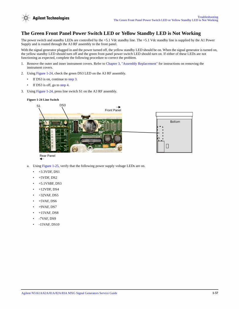
Troubleshooting The Green Front Panel Power Switch LED or Yellow Standby LED is Not Working
The Green Front Panel Power Switch LED or Yellow Standby LED is Not WorkingThe power switch and standby LEDs are controlled by the +5.1 Vdc standby line. The +5.1 Vdc standby line is supplied by the A1 Power Supply and is routed through the A3 RF assembly to the front panel.
With the signal generator plugged in and the power turned off, the yellow standby LED should be on. When the signal generator is turned on, the yellow standby LED should turn off and the green front panel power switch LED should turn on. If either of these LEDs are not functioning as expected, complete the following procedure to correct the problem.
1. Remove the outer and inner instrument covers. Refer to Chapter 3, "Assembly Replacement" for instructions on removing the instrument covers.
2. Using Figure 1-24, check the green DS3 LED on the A3 RF assembly.
• If DS3 is on, continue to step 3.
• If DS3 is off, go to step 4.
3. Using Figure 1-24, press line switch S1 on the A3 RF assembly.
Figure 1-24 Line Switch
a. Using Figure 1-25, verify that the following power supply voltage LEDs are on.
• +3.3VDF, DS1
• +5VDF, DS2
• +5.1VSBF, DS3
• +12VDF, DS4
• +32VAF, DS5
• +5VAF, DS6
• +9VAF, DS7
• +15VAF, DS8
• -7VAF, DS9
• -15VAF, DS10
DS3S1Front Panel
Rear Panel
Agilent N5161A/62A/81A/82A/83A MXG Signal Generators Service Guide 1-57
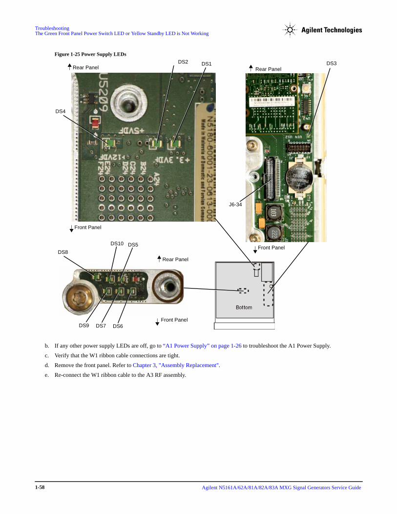
TroubleshootingThe Green Front Panel Power Switch LED or Yellow Standby LED is Not Working
Figure 1-25 Power Supply LEDs
b. If any other power supply LEDs are off, go to “A1 Power Supply” on page 1-26 to troubleshoot the A1 Power Supply.
c. Verify that the W1 ribbon cable connections are tight.
d. Remove the front panel. Refer to Chapter 3, "Assembly Replacement".
e. Re-connect the W1 ribbon cable to the A3 RF assembly.
Front Panel
Rear Panel
Front Panel
Front Panel
Rear Panel
DS8
DS3DS1Rear Panel
DS2
DS4
DS9 DS7 DS6
DS10 DS5
J6-34
Agilent N5161A/62A/81A/82A/83A MXG Signal Generators Service Guide 1-58

Troubleshooting The Green Front Panel Power Switch LED or Yellow Standby LED is Not Working
f. See Figure 1-26. Use a voltmeter with a small probe to measure the output voltage +5.1V on the A6 DC-AC Inverter Interface assembly at J1-34.
• If the voltage is within limits, the fault is likely with the A6 DC-AC Inverter Interface Board. Refer to “A6 DC-AC Inverter Interface Board (N5181A/82A/83A)” on page 1-34 to troubleshoot.
• If the voltage is not within limits, measure J6-34 on the A3 RF assembly. Refer to Figure 1-25.
— If the voltage is within limits, replace W1.
— If the voltage is not within limits, go to step 4.
Figure 1-26 +5.1V on A6 at J1-34
4. See Figure 1-27. Use a voltmeter with a small probe to measure the output voltage +5.1SB on the A3 RF assembly at J10-F23.
Figure 1-27 +5.1SB at J10-F23
• If the voltage is not within limits, the fault is likely with the A1 Power Supply. Replace the A1 Power Supply.
• If the voltage is within limits:
J1-34
A3J10-F23
Agilent N5161A/62A/81A/82A/83A MXG Signal Generators Service Guide 1-59

TroubleshootingFront Panel Hardkeys or Softkeys are Not Functioning (N5181A/82A/83A)
a. Replace the A3 RF assembly.
b. For N5183A instruments, go to Chapter 4, "Post-Repair Procedures and Performance Verification".
Front Panel Hardkeys or Softkeys are Not Functioning (N5181A/82A/83A)Verify individual key functionality by performing the Front Panel Key Test. Pressing each key should darken the location on the front panel associated with that key.
Press: Utility > Instrument Info > Front Panel Tests > Key Test
• If intermittent operation occurs, replace the Key Pad assembly.
• If more than 50% of the keys do not cause the corresponding test area to change color, replace the A6 DC-AC Inverter Interface Board.
The RPG Knob is Not Functioning (N5181A/82A/83A)Verify the RPG functionality by performing the front panel RPG test.
Press: Utility > Instrument Info > Front Panel Tests > RPG Test
• Turning the RPG knob to the right should cause positive incremental changes; expected range +10.
• Turning the RPG knob to the left should cause negative incremental changes; expected range −10.
Figure 1-28 A6 DC-AC Inverter Interface Board
A6J1-11 and A6J1-12A6J2-25
A6J2-28
A6J1-3 and A6J1-4
Agilent N5161A/62A/81A/82A/83A MXG Signal Generators Service Guide 1-60

Troubleshooting The RPG Knob is Not Functioning (N5181A/82A/83A)
Figure 1-29 A3J6 and A3J10
If the RPG test fails, complete the following procedure to determine the faulty assembly/part:
1. Remove the front panel. Refer to Chapter 3, "Assembly Replacement".
2. Refer to Figure 1-28. Verify that A6J2-25 has a voltage of +3 Vdc:
• If A6J2-25 has a voltage of +3 Vdc, go to step 10.
• If A6J2-25 does not have a voltage of +3 Vdc, go to step 3.
3. Refer to Figure 1-28. Measure A6J1-11 and A6J1-12; they should have a voltage of +3 Vdc.
• If A6J1-11 and A6J1-12 have a voltage of +3 Vdc, replace the A6 DC-AC Inverter Interface Board.
• If A6J1-11 and A6J1-12 do not have a voltage of +3 Vdc, go to step 4.
4. Refer to Figure 1-29. Measure A3J6-11 and A3J6-12; they should have a voltage of +3 Vdc.
• If A3J6-11 and A3J6-12 have a voltage of +3 Vdc, replace the W1 ribbon cable.
• If A3J6-11 and A3J6-12 do not have a voltage of +3 Vdc, go to step 5.
5. Refer to Figure 1-29. Measure A3J10-A21 and A3J10-A22; they should have a voltage of +3 Vdc.
• If A3J10-A21 and A3J10-A22 have a voltage of +3 Vdc:
a. Replace the A3 RF assembly.
b. After replacing the A3 RF assembly in a model N5183A instrument, go to Chapter 4, "Post-Repair Procedures and Performance Verification".
• If A3J10-A21 and A3J10-A22 do not have a voltage of +3 Vdc, go to “A1 Power Supply” on page 1-26 to troubleshoot the A1 Power Supply.
6. Refer to Figure 1-28. Measure A6J2-28; it should have a voltage of +5 Vdc.
• If A6J2-28 has a voltage of +5 Vdc, go to step 10.
• If A6J2-28 does not have a voltage of +5 Vdc, go to step 7.
A3J611 and A3J6-12
A3J10-A21 and A3J10-A22
Front Panel
Rear Panel
Rear Panel
Front Panel
A3J6-3 and A3J6-4
A3J10-B16
Agilent N5161A/62A/81A/82A/83A MXG Signal Generators Service Guide 1-61

TroubleshootingBlank or Missing Pixels (N5181A/82A/83A)
7. Refer to Figure 1-28. Measure A6J1-3 and A6J1-4; they should have a voltage of +12 Vdc.
• If A6J1-3 and A6J1-4 have a voltage of +12 Vdc, replace the A6 AC-DC Inverter Interface Board.
• If A6J1-3 and A6J1-4 do not have a voltage of +12 Vdc, go to step 8.
8. Refer to Figure 1-29. Measure A3J6-3 and A3J6-4; they should have a voltage of +12 Vdc.
• If A3J6-3 and A3J6-4 have a voltage of +12 Vdc, replace the W1 ribbon cable.
• If A3J6-3 and A3J6-4 do not have a voltage of +12 Vdc, go to step 9.
9. Refer to Figure 1-29. Measure A3J10-B16; it should have a voltage of +12 Vdc.
• If A3J10-B16 has a voltage of +12 Vdc:
a. Replace the A3 RF assembly.
b. For N5183A instruments, go to Chapter 4, "Post-Repair Procedures and Performance Verification".
• If A3J10-B16 does not have a voltage of +3 Vdc, go to “A1 Power Supply” on page 1-26 to troubleshoot the A1 Power Supply.
10. Refer to Figure 1-28. Using an oscilloscope, turn the RPG knob and measure A6J2-26 and A6J2-30. There should be a 4V square pulse. If there is no 4V square pulse, replace the Keypad assembly.
Blank or Missing Pixels (N5181A/82A/83A)Verify functionality by performing the front panel LCD Pixel tests.
Press: Utility > Instrument Info > Front Panel Tests > Pixel Screen Tests
• If the same area of the display is blank during each pixel test, replace the LCD Display.
• If an area of the display is only blank during some of the tests, replace the A6 DC-AC Inverter Interface board.
The Screen Saver is Not Functioning (N5181A/82A/83A)The screen saver delay can be set from 1 to 12 hours. The PIC Controller controls the screen saver by turning the LCD backlight on or off.
1. Verify the signal generator is turned on.
2. Set the delay time to 1 hour. Press: Utility > Display > Screen Saver Delay, then turn the RPG knob.
3. Allow the screen saver delay time to elapse.
4. Check to see if the display has gone dark.
5. If the display has not gone dark, replace the A6 DC-AC Inverter Interface assembly.
6. Set the delay time to 1 hour.
7. Allow the screen saver delay time to elapse.
8. Check to see if the display has gone dark.
9. If the display still has not gone dark, replace the A5 CPU assembly.
Boot Time Diagnostics Mode (N5161A/62A Only)
CAUTION This section should only be used by qualified service personnel.
This procedure serves as a full test of the front panel on an MXG ATE, as the LEDs and LAN Reset key must be functioning properly in order for the instrument to proceed to the next mode.
To run the boot time diagnostics mode:
1. Turn the instrument off.
2. Press and hold the LAN Reset hardkey then press and release the power switch, until the 3 front panel LEDs start blinking. They will blink for approximately 10 seconds.
Agilent N5161A/62A/81A/82A/83A MXG Signal Generators Service Guide 1-62

Troubleshooting Boot Time Diagnostics Mode (N5161A/62A Only)
3. Release the LAN Reset hardkey. When the LEDs stop blinking, the instrument has entered the diagnostic mode.
• If the LAN Reset key is pressed again within the 5 seconds, the next blink pattern will be shown and the 5 second wait starts over.
• If the LAN Reset key is not pressed again within 5 seconds, the currently displayed diagnostic mode will be executed (and the instrument will finish booting).
The LEDs blink in certain patterns as indicated in the following table.
NOTE The LED blink patterns are cyclic. With the exception of the first pattern, one of them must be chosen to finish booting.
The first pattern is the recommended diagnostic mode.
Exceptions - Auto-reboot, ERROR LED Blinking (N5161A/62A Only)
Auto-reboot is enabled using the SCPI command :DIAGnostic:FMWR:VAR |1|ON|0|OFF|.
1. When an exception occurs, the MXG ATE instrument will automatically reboot.
2. The exception is reported in an error message upon the next bootup.
3. This exception is logged to file location "/sys/exceptionLog.txt" and renamed "/sys/exceptionLogOld.txt" once it has been reported.
4. If another exception occurs during the next bootup, and there was an exception reported during the previous bootup, the instrument will stop and blink the ERROR LED.
If auto-reboot is disabled and an exception occurs, the instrument will stop and blink the ERROR LED.
Via LAN or USB, use the Web-Enabled MXG to check the Error Queue. Refer to “Accessing the MXG Web-Enabled Page” on page 1-18 and to “Running Self Test” on page 1-16.
5. Clear the Error Queue and cycle power on the instrument. Refer to the User’s Guide.
6. If another exception occurs during the next bootup, press the front panel’s LAN Reset hardkey.
7. If another exception occurs during the next bootup, refer to “A5 CPU Assembly Troubleshooting” on page 1-33.
Table 1-9 Diagnostics Mode (N5161A/62A)
LAN 1588 ERROR Diagnostic Mode
- - - Force Volume Verification. This diagnostic mode verifies the internal hardware connections.
- - B Recover from failed firmware update (No Hardware Mode, Ignore User Preset, and Don't Load Selftest and Calibration Modules) (try first).
- B - Recover from failed firmware update and Preset Persistent values (try second).
- B B Backup License Data.
B - - Restore License Data.
Table Legend
- LED is continuously Off.
BLED is continuously blinking.
Agilent N5161A/62A/81A/82A/83A MXG Signal Generators Service Guide 1-63

TroubleshootingThe Fans are Not Working
The Fans are Not WorkingThe four fans are connected directly to the A1 Power Supply. The fan motors are AC motors, with a DC to AC inverter built into the motor hub. The control, voltage, and filtering for the fans are integrated into the A1 Power Supply. The fan control voltage is a nominal 12 Vdc. The control range can vary from a minimum of 8 volts up to a maximum of 13.8 volts. Using internal sensors, the control circuit sets the fan voltage to adjust the fan speed to protect the A1 Power Supply and the signal generator. The A1 Power Supply will function at full output load, up to 25° C, without raising the minimum fan voltage. The A1 Power Supply may begin to raise the fan voltage at 25° C and will reach maximum voltage at no lower than 45° C ambient.
• If a single fan is inoperative, the most likely cause is a faulty fan.
1. Unplug the inoperative fan and one working fan.
2. Plug the inoperative fan into the working fan’s connector on the A1 Power Supply.
— If the inoperative fan works, the connector on the A1 Power Supply is faulty. Replace the A1 Power Supply.
— If the inoperative fan does not work, plug the good fan into the inoperative fan’s connector on the A1 Power Supply. If the good fan works, the inoperative fan is faulty. Replace the fan.
• If two or more fans are inoperative, the most likely assembly at fault is the A1 Power Supply. The four fans are connected in parallel, so if the A1 Power Supply voltage is faulty for one fan, then by design, the voltage will be faulty for all four fans. Replace the A1 Power Supply.
No LAN ActivityThe signal generator supports 100-Base T-LAN. When the signal generator is connected to an active LAN, one of the green DS1 LEDs, viewable through the rear panel, will be on and the other green DS1 LED will blink.
• If either of the DS1 LEDs do not respond to an active LAN connection, replace the A5 CPU assembly.
No Front Panel USB ActivityThe front panel Type-A USB connector supports data transfers.
NOTE Not all USB memory sticks are compatible with the Type-A USB connector on this signal generator. Go to www.agilent.com/find/mxg for a list of USB storage devices that work with this signal generator.
1. Connect a compatible USB memory stick to the signal generator. The signal generator should detect the USB memory stick immediately.
2. If a compatible memory stick does not work, but the rear panel USB and all other instrument functions operate correctly, replace the USB Board.
3. If replacing the USB Board does not correct the problem, replace the A5 CPU assembly.
No Rear-Panel USB Activity
NOTE Not all Mini-B USB cables provide enough connector length to ensure proper contact between the cable and the Mini-B 5 USB connector on the MXG.
The rear-panel type Mini-B 5 pin USB connector is used for remotely controlling the signal generator using SCPI commands.
1. Connect a USB cable between a controller PC that has been configured to communicate through a USB cable and the signal generator. The PC should detect the signal generator almost immediately.
2. If the signal generator is not detected:
a. Verify the rear-panel Mini-B USB cable is inserted deeply enough to make proper contact.
b. If the rear-panel Mini-B USB cable is inserted deeply enough to make proper contact, replace the A5 CPU assembly.
Agilent N5161A/62A/81A/82A/83A MXG Signal Generators Service Guide 1-64

Troubleshooting No GPIB Activity
No GPIB ActivityThe signal generator supports a general purpose interface bus (GPIB). The GPIB enables communication with compatible devices such as external controllers.
1. Replace the GPIB cable with a known working cable.
2. Send a SCPI command to the signal generator.
3. Verify the signal generator responds to the SCPI command.
4. If the signal generator does not respond to the SCPI command, replace the A5 CPU assembly.
Error Messages For more information on Error Messages go to the error messages list on the documentation CD, N5180-90007, or online at http://cp.literature.agilent.com/litweb/pdf/N5180-90020.pdf.
Troubleshooting UnlocksThe phase lock loop refers to the frequency generating circuit used to maintain the phase relationship between the frequency generation loop and a reference frequency. By maintaining the phase relationship, the frequency accuracy of the signal generator is guaranteed.
To maintain accuracy, the phase lock loop compares the phase of a signal from the reference assembly to the phase of the frequency loop signal. If the two signals are out of phase, the phase comparator circuit adjusts the frequency loop signal until the signals are in phase. If the phase comparator circuit cannot adjust the phase of the frequency loop signal, the phase comparator rails and generates an unlocked message. The unlock message will be displayed on the front panel.
Troubleshoot multiple loop unlock messages in the following order:
1. “508 Frac-N Loop Unlock” on page 1-65
2. “512 Reference Unlocked” on page 1-65
3. “515 Reference Missing” on page 1-66
4. “532 PCI Bridge FPGA DCM Unlocked” on page 1-66
5. “533 RF Analog FPGA DCM Unlocked” on page 1-66
508 Frac-N Loop Unlock
A 508 Frac-N Loop Unlock message indicates a problem with the Voltage Control Oscillator's (VCO) phase-locked loop on the A3 RF assembly.
• If the signal generator is connected to an external reference:
1. Check the reference’s frequency, power, and physical connection.
2. Make sure the external reference frequency, specified in the instrument setup, is correct.
3. If the external reference signal and connection is good, replace the A3 RF Assembly.
• If the signal generator is not connected to an external reference:
1. Replace the A3 RF assembly.
2. For N5183A instruments, go to Chapter 4, "Post-Repair Procedures and Performance Verification".
512 Reference Unlocked
A 512 Reference Unlocked message indicates a problem with the external reference settings or connections.
• If the signal generator is connected to an external reference:
1. Check the reference’s frequency, power, and physical connection.
2. Make sure the external reference frequency, specified in the instrument setup, is correct.
3. If the external reference signal and connection is good, replace the A3 RF Assembly.
Agilent N5161A/62A/81A/82A/83A MXG Signal Generators Service Guide 1-65

TroubleshootingTroubleshooting Unlevels
• If the signal generator is not connected to an external reference:
1. Replace the A3 RF assembly.
2. For N5183A instruments, go to Chapter 4, "Post-Repair Procedures and Performance Verification".
515 Reference Missing
A 515 Reference Missing message indicates the Reference circuit’s 10 MHz reference signal is bad or missing. The signal generator’s reference is unlocked.
• If the signal generator is connected to an external reference:
1. Check the reference’s frequency, power, and physical connection.
2. Make sure the external reference frequency, specified in the instrument setup, is correct.
3. If the external reference signal and connection is good, replace the A3 RF Assembly.
• If the signal generator is not connected to an external reference:
1. Replace the A3 RF assembly.
2. For N5183A instruments, go to Chapter 4, "Post-Repair Procedures and Performance Verification".
532 PCI Bridge FPGA DCM Unlocked
A 532 PCI Bridge FPGA DCM Unlocked message indicates that the PCI Bridge FPGA clocks are not working correctly.
• If this message appears:
1. Replace the A3 RF assembly.
2. For N5183A instruments, go to Chapter 4, "Post-Repair Procedures and Performance Verification".
533 RF Analog FPGA DCM Unlocked
A 533 RF Analog FPGA DCM Unlocked message indicates the FPGA clocks are not working correctly.
• If this message appears:
1. Replace the A3 RF assembly.
2. For N5183A instruments, go to Chapter 4, "Post-Repair Procedures and Performance Verification".
Troubleshooting UnlevelsAn Automatic Leveling Control (ALC) loop on the A3 RF assembly provides leveled output power. The ALC loop is a feedback control system that monitors RF power and maintains power at the user-selected level. The RF path must provide a minimum power level to the ALC loop for the ALC loop to work correctly. The minimum required power is slightly higher than the instrument maximum power level.
A leveled output power is obtained by comparing a detected voltage with a reference voltage. The detected voltage is generated by coupling off a portion of the RF output signal and converting it to a dc voltage using detector diodes. The reference voltage is generated using calibrated DAC’s. When the reference and detected levels are not the same, the ALC integrator output ramps up or down, to increase or decrease the detected level. If the integrator cannot achieve a match between the detected and reference voltages an unleveled annunciator is displayed.
1. Run a complete self test.
Press: Utility > Instrument Info > Self Test > Run Complete Self Test.
2. Troubleshoot any unlocks.
Refer to “Troubleshooting Unlocks” on page 1-65.
3. Measure the output power at the RF connector.
4. Check the measured output power level against the values in Table 1-10 or Table 1-12.
NOTE The output power values shown in these tables might not apply to your specific signal generator configuration. Refer to the current data sheet for the latest power level data.
Agilent N5161A/62A/81A/82A/83A MXG Signal Generators Service Guide 1-66

Troubleshooting Troubleshooting Unlevels
• If the signal generator is an N5181A and it does not meet the listed power level in Table 1-10, proceed to “Troubleshooting the RF Path (N5161A/62A/81A/82A)” on page 1-68.
• If the signal generator is an N5162A/82A and does not achieve the maximum power levels listed in Table 1-10, perform the following procedure:
Press
1. Mode > Dual Arb > Arb Off/On - until Off is highlighted
2. Press Mode > Real Time I/Q Baseband AWGN > Real-time AWGN Off/On - until Off is highlighted
Table 1-10N5181A/82A Output Power
Frequencies Output Power (All Instruments with serial prefixes <4740 and without Option 099 or Option 01K.)
Output Power (All Instruments with serial prefixes >4740 or all instruments with Option 01K.)
100 kHz to <250 kHz N/A +4 dBm
≥250 kHz to 2.5 GHz +13 dBm +13 dBm
>2.5 GHz to 3.0 GHz +10 dBm +10 dBm
>3.0 GHz to 4.5 GHz +13 dBm +13 dBm
>4.5 GHz to 5.8 GHz +10 dBm +10 dBm
>5.8 GHz to 6 GHz +7 dBm +7 dBm
Table 1-11 N5161A/62A/81A/62A/82A Output Powera
aAll instruments with serial number > xx4818xxx and all instruments with serial number < xx4818xx with Option 099.
Frequencies Output Power
100 kHz to 50 MHz +13 dBm
>50 MHz to 3 GHz +13 dBm
>3.0 GHz to 5.0 GHz +13 dBm
>5.0 GHz +11 dBm
Table 1-12N5183A Output Power
Frequencies Output Power N5183A with Opt 520
Output Power N5183A with Opt 520 and Opt 1EA
Output Power N5183A with Opt 532 and Opt 540
Output Power N5183A with Opt 532, Opt 540, and Opt 1EA
100 kHz to 250 kHz +11 dBm +14 dBm +11 dBm +14 dBm
>250 kHz to 3.2 GHz +11 dBm +15 dBm +7 dBm +15 dBm
>3.2 GHz to 20 GHz +11 dBm +18 dBm N/A N/A
>3.2 GHz to 17 GHz N/A N/A +7 dBm +15 dBm
>17 GHz to 31.8 GHz N/A N/A +7 dBm +13 dBm
>31.8 GHz to 40 GHz N/A N/A +7 dBm +12 dBm
Agilent N5161A/62A/81A/82A/83A MXG Signal Generators Service Guide 1-67
TroubleshootingTroubleshooting the RF Path (N5161A/62A/81A/82A)
3. Using Table 1-10, re-check the maximum power levels.
— If the signal generator meets its maximum power levels, proceed to “Troubleshooting the RF Path (N5161A/62A/81A/82A)” on page 1-68.
— If the signal generator does not achieve the maximum power levels:
a. Replace the A2 Vector Module assembly.
b. Proceed to “Troubleshooting the RF Path (N5161A/62A/81A/82A)” on page 1-68.
• If the signal generator is an N5183A and it does not meet one or more of the listed power levels in Table 1-12, perform the troubleshooting procedure for the frequency range in which the low power occurred:
— “No Output Power or Output Power is Unleveled (N5183A)” on page 1-40
— “Low Output Power or No Output Power < 3.2 GHz (N5183A)” on page 1-41
— “Low Output Power or No Output Power >= 3.2 GHz (N5183A)” on page 1-46
Troubleshooting the RF Path (N5161A/62A/81A/82A)The ALC loop circuitry is part of the A3 RF assembly. It is likely an unleveled or under power condition is the result of a problem with the A3 RF assembly.
• For an N5161A/81A signal generator, replace the A3 RF assembly.
• For an N5162A/82A signal generator,
1. Verify that the A2 Vector Module is not contributing to the unleveled or under power condition. Refer to “A2 Vector Module Troubleshooting (N5162A/82A Only)” on page 1-29.
2. If the A2 Vector Module is not contributing to the condition, replace the A3 RF assembly.
Troubleshooting the 6 GHz Electronic Attenuator (N5161A/62A/81A/82A)The 6 GHz electronic attenuator is built into the A3 RF assembly. It has an attenuation range of 130 dB, in 5 dB steps. The attenuator is used to rough tune the power level, while the ALC loop is used to fine-tune the power level. (The ALC fine tunes the power level within each 5 dB step.) Due to the interactive design of the attenuator and the ALC loop, there is no precise setting that will predict when the attenuator will be switched in. The firmware, along with the selected frequency, the current ALC setting, modulation, and the requested attenuation all work together to determine the optimum instrument performance and when an attenuation step is switched in.
Aside from an A1 Power Supply failure, any suspected improper functionality of the attenuator requires the replacement of the A3 RF assembly.
The best way to troubleshoot the 6 GHz Electronic Attenuator is to run self test “601 Attenuator Voltages”. If this self-test cannot be run, perform the following steps:
1. Refer to Figure 1-30. Use a voltmeter with a small probe to measure the output voltage +5.1V at J10-F23 and +/-15V at J10-A1 and J10-A3 on the A3 RF assembly.
Agilent N5161A/62A/81A/82A/83A MXG Signal Generators Service Guide 1-68

Troubleshooting Troubleshooting Harmonic Spurious
Figure 1-30 +5.1V and +/-15V
• If the voltages are within limits, the A1 Power Supply is not at fault. Replace the A3 RF assembly.
• If any voltages are incorrect, the faulty assembly could be either the A1 Power Supply or the A3 RF assembly.
a. Replace the A1 Power Supply1.
b. Repeat step 1.
c. If the voltages are still incorrect replace the A3 RF assembly.
Troubleshooting Harmonic SpuriousHarmonics are multiples of the fundamental output frequency produced by a signal generator. Specifically, the second harmonic is two times the output frequency and its amplitude is measured relative to the fundamental (carrier) output frequency amplitude; the power lever of a harmonic is expressed as -xx dBc.
• If the frequency of a harmonic falls beyond the frequency range of the signal generator, that particular harmonic is not specified or measured.
• If the frequency of a harmonic falls within the frequency range of the signal generator, the harmonic’s power level is obtained with the following procedure:
1. Set the signal generator and spectrum analyzer to the same harmonic frequency.
2. Set the signal generator to a specific power level. Its output peak power level is measured on the spectrum analyzer; this peak power level is the reference level used for the harmonic measurement.
3. Set the signal generator to the fundamental frequency. The power level of the fundamental frequency is measured by using Peak Search and Marker Delta.
This measurement obtains the power level of the harmonic and is expressed as a dBc value; it is the difference between the fundamental peak power level and the harmonic frequency power level.
1If you replaced the A1 Power Supply, but the A3 RF assembly was the faulty assembly, you can return the new A1 Power Supply to Agilent.
F23
A3 A1
Agilent N5161A/62A/81A/82A/83A MXG Signal Generators Service Guide 1-69
TroubleshootingTroubleshooting Harmonic Spurious
Troubleshooting Harmonic Spurious by Fundamental Frequency
All mixing products and by-products are generated on the A3 RF assembly. Harmonic spurious problems will most likely be associated with the A3 RF assembly.
• Spurious harmonic levels beyond the published specifications of the N5181A/82A require the replacement of the A3 RF assembly.
To Verify Harmonic Performance at the RF Output1. Signal Generator Settings
a. Set the frequency of the signal generator to the harmonic frequency being measured. For example, when planning to measure the second harmonic of a 1 GHz signal, set the frequency of the signal generator to 2 GHz.
b. Set the power level of the signal generator to +4 dBm (+7.5 dBm for Option UNB).
2. Spectrum Analyzer Settings
a. Connect a spectrum analyzer to the RF Output connector of the signal generator.
b. Set the frequency of the spectrum analyzer to the harmonic frequency being measured. To continue with our example, set the frequency of the spectrum analyzer to 2 GHz.
c. On the spectrum analyzer, press the Peak Search and Marker Delta keys. The marker should indicate approximately 0 dBm.
3. Signal Generator Settings
a. Set the signal generator to the fundamental frequency of the harmonic being measured. In this example, because the measured harmonic was at 2 GHz, the signal generator should be set to 1 GHz.
4. Spectrum Analyzer Settings
a. On the spectrum analyzer, read the power level (and record it for future reference, in case further troubleshooting is necessary). The marker should indicate a power level in dBc; this is the power level of the harmonic being measured.
b. Compare the power level of the marker against the specified harmonic performance level for your signal generator.
Agilent N5161A/62A/81A/82A/83A MXG Signal Generators Service Guide 1-70

Troubleshooting Troubleshooting Non-Harmonic Spurious
Troubleshooting Non-Harmonic SpuriousNon-harmonic spurious responses are unwanted signals that are not related to the fundamental output frequency but are produced by the internal frequency synthesis section of the signal generator. There are many different groupings a spur can fall into. The grouping determines what assembly is most likely generating the spur.
Spur types for this signal generator are noted in Table 1-13. To troubleshoot spurs:
1. Identify the grouping based on failing a specified performance test.
2. Check for loose or broken cables and castings.
3. Replace the assembly.
Table 1-13
Type of Spur Options Description Replace
Reference Spurs All These spurs are generated by the 10 MHz frequency reference on the A3 RF assembly.
A3 RF assemblya
aAfter replacing the A3 RF assembly in a model N5183A instrument, go to Chapter 4, "Post-Repair Procedures and Performance Verification".
Mixing Spurs All These spurs are generated by the mixing products of the RF and IF signals on the A3 RF assembly. The signal generator is tuned to a frequency in the Heterodyne band (≤250 MHz) to measure these spurs.
A3 RF assemblya
Power Supply Spurs All These spurs are generated by the power supply switching at a 120 kHz rate.
A1 Power Supply
LO Feedthru Spurs All These spurs are generated by the LO signal passing through the mixer in the Heterodyne band.
A3 RF assemblya
RF Feedthru Spurs All These spurs are generated by the RF signal passing through the mixer in the Heterodyne band.
A3 RF assemblya
Agilent N5161A/62A/81A/82A/83A MXG Signal Generators Service Guide 1-71
TroubleshootingTroubleshooting Performance Test Problems
Troubleshooting Performance Test ProblemsThis section describes the available Agilent MXG signal generator performance tests. These performance tests verify that the signal generator meets specifications.
IMPORTANT All test equipment configurations, cables and adapters must be properly torqued. Exceeding recommended torque values can cause damage to a cable or adapter, and may cause inaccurate test results.
Manual Performance Test Problems
When a manual performance test fails or self tests, performed as part of the manual performance test, fails, use this table to locate the most likely faulty assembly or action to perform. The tests are listed in the order they should be performed.
Performance test that is failing... Action to perform...
I/Q Calibration (N5162A/82A only) • Replace the A2 Vector Module assembly.
Self-Tests • Go to “Running Self Test” on page 1-16.
Relative Frequency Range and Accuracy Verification • Replace the A3 RF assemblya.
aAfter replacing the A3 RF assembly in a model N5183A instrument, go to Chapter 4, "Post-Repair Procedures and Performance Verification".
Leveled Output Power Verification • For the N5161A/81A signal generator, replace the A3 RF assembly.
• For the N5162A/82A signal generator, ensure that digital modulation is turned off by pressing the following keys:
1. Mode > Dual Arb > Arb Off/On - until Off is highlighted
2. Mode > Real Time I/Q Baseband AWGN > Real-time AWGN Off/On - until Off is highlighted
3. Re-run the Leveled Output Power Verification test.
— If the signal generator passes the Leveled Output Power Verification test, replace the A2 Vector Module.
— If the signal generator does not pass the Leveled Output Power Verification test, replace the A3 RF assembly.
• For the N5183A signal generator, go to “No Output Power or Output Power is Unleveled (N5183A)” on page 1-40.
Phase Noise (N5183A only) • Replace the A3 RF assemblya.
Agilent N5161A/62A/81A/82A/83A MXG Signal Generators Service Guide 1-72

Troubleshooting Troubleshooting Performance Test Problems
Troubleshooting Adjustment Test Problems (N5183A Only)
The table below shows the assemblies to replace to correct specific adjustment failures. Before you replace an assembly because of an adjustment failure, perform the following procedure:
1. Confirm that all self tests passed.
2. Confirm that all required test equipment is in good operating condition and is correctly connected.
3. Repeat the adjustment.
• If the adjustment still fails, replace the first assembly listed in the table for the adjustment that is failing.
4. Repeat the adjustment.
• If the adjustment still fails, replace the second assembly listed in the table for the adjustment that is failing.
5. Go to Chapter 4, "Post-Repair Procedures and Performance Verification".
Automated Performance Test Problems
If the self-tests pass, but an automated performance test fails, use this table to locate the assembly that is most likely to have failed. To avoid unnecessary reconfiguration of test equipment, run the performance tests in the order in which they are listed in the table. Always use the latest revision of the service software.
Adjustment that is failing... Assembly to replace
Microwave multiplier prelevel calibration A7 Micro Deck
AM calibration 1. A3 RF Assembly
2. A7 Micro Deck
Limited absolute power calibration A7 Micro Deck
ALC mod driver calibration (fails in the low frequency band) A3 RF Assembly
ALC mod driver calibration (fails in the high frequency band) A7 Micro Deck
Performance Test that is Failing... Action to Perform... (N5161A/81A/62A/82A)
Action to Perform... (N5183A)
Digital Modulation Power Level Accuracy Relative to (N5162A/82A only)
Replace the A3 RF assembly N/A
Power Level Accuracy Replace the A3 RF assembly If a failure occurs at ≥ 3.2 GHz, replace the A7
Micro Decka. If failure occurs at < 3.2 GHz, replace the A3
RF assemblya.
Harmonic Spurious Replace the A3 RF assembly Replace the A3 RF assemblya.
Sub-Harmonic Spurious Replace the A3 RF assembly Replace the A3 RF assemblya.
Non-Harmonic Spurious Replace the A3 RF assembly Replace the A3 RF assemblya.
WCDMA Adjacent Channel Power (N5162A/82A only)
1. Rerun the test at a power level of −7 dBm.
2. Reduce the power level by 1 dB and repeat test.
3. Repeat the test three more times, reducing the power level by 1 dB each time.
• If the ACP performance improves, replace the A3 RF assembly.
• If the ACP performance remains consistent or degrades, replace the A2 Vector Module.
N/A
FM Deviation Accuracy Replace the A3 RF assembly Replace the A3 RF assemblya.
Agilent N5161A/62A/81A/82A/83A MXG Signal Generators Service Guide 1-73
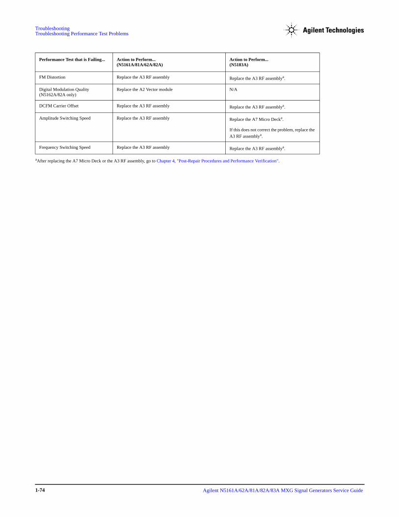
TroubleshootingTroubleshooting Performance Test Problems
FM Distortion Replace the A3 RF assembly Replace the A3 RF assemblya.
Digital Modulation Quality (N5162A/82A only)
Replace the A2 Vector module N/A
DCFM Carrier Offset Replace the A3 RF assembly Replace the A3 RF assemblya.
Amplitude Switching Speed Replace the A3 RF assembly Replace the A7 Micro Decka. If this does not correct the problem, replace the
A3 RF assemblya.
Frequency Switching Speed Replace the A3 RF assembly Replace the A3 RF assemblya.
aAfter replacing the A7 Micro Deck or the A3 RF assembly, go to Chapter 4, "Post-Repair Procedures and Performance Verification".
Performance Test that is Failing... Action to Perform... (N5161A/81A/62A/82A)
Action to Perform... (N5183A)
Agilent N5161A/62A/81A/82A/83A MXG Signal Generators Service Guide 1-74

2 Replaceable Parts
Ordering InformationTo order a part, do the following:
1. Determine the part number.
2. Determine the quantity required.
3. Mail this information to the nearest Agilent Technologies office or, in the U.S., call the hot-line number listed in the following section.
To order a part not listed in the replaceable parts lists, mail the following information to the nearest Agilent Technologies office.
1. the instrument model number
2. the serial number and options, if any (see rear panel)
3. a description of the part
4. a description of the part’s function
5. the quantity required
Order Parts Fast
When you have gathered the information required to place an order, go to the Agilent Technologies Technical Support website: http://www.agilent.com/find/techsupport
Shipping a Defective Assembly Back to Agilent Technologies1. When you receive the rebuilt/exchange assembly, be careful not to damage the box and shipping hardware in which it was shipped. You
will use that box and shipping hardware to return the defective assembly. The box you receive should contain the following:
• the rebuilt assembly
• an exchange assembly failure report
• a return address label
2. Complete the failure report.
3. Place the failure report and the defective assembly in the box. Be sure to remove the enclosed return address label.
4. Seal the box with tape.
If you are inside the United States, stick the pre-printed return address label over the label that is already on the box and return the box to Agilent Technologies. (Agilent Technologies pays postage on boxes mailed within the United States.)
If you are outside the United States, do not use the return address label; instead, address the box to the nearest Agilent Technologies sales and service office.
Agilent N5161A/62A/81A/82A/83A MXG Signal Generators Service Guide 2-1
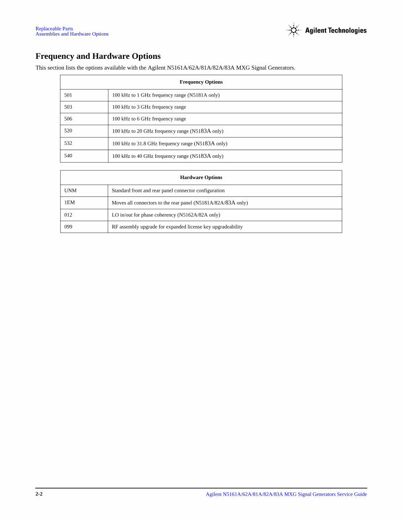
Replaceable Parts Assemblies and Hardware Options
Frequency and Hardware OptionsThis section lists the options available with the Agilent N5161A/62A/81A/82A/83A MXG Signal Generators.
Frequency Options
501 100 kHz to 1 GHz frequency range (N5181A only)
503 100 kHz to 3 GHz frequency range
506 100 kHz to 6 GHz frequency range
520 100 kHz to 20 GHz frequency range (N5183A only)
532 100 kHz to 31.8 GHz frequency range (N5183A only)
540 100 kHz to 40 GHz frequency range (N5183A only)
Hardware Options
UNM Standard front and rear panel connector configuration
1EM Moves all connectors to the rear panel (N5181A/82A/83A only)
012 LO in/out for phase coherency (N5162A/82A only)
099 RF assembly upgrade for expanded license key upgradeability
Agilent N5161A/62A/81A/82A/83A MXG Signal Generators Service Guide2-2
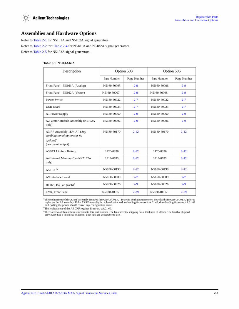
Replaceable Parts Assemblies and Hardware Options
Assemblies and Hardware OptionsRefer to Table 2-1 for N5161A and N5162A signal generators.
Refer to Table 2-2 thru Table 2-4 for N5181A and N5182A signal generators.
Refer to Table 2-5 for N5183A signal generators.
Table 2-1 N5161A/62A
Description Option 503 Option 506
Part Number Page Number Part Number Page Number
Front Panel - N5161A (Analog) N5160-60005 2-9 N5160-60006 2-9
Front Panel - N5162A (Vector) N5160-60007 2-9 N5160-60008 2-9
Power Switch N5180-60022 2-7 N5180-60022 2-7
USB Board N5180-60023 2-7 N5180-60023 2-7
A1 Power Supply N5180-60060 2-9 N5180-60060 2-9
A2 Vector Module Assembly (N5162A only)
N5180-69006 2-9 N5180-69006 2-9
A3 RF Assembly 1EM All (Any combination of options or no options)a (rear panel output)
aThe replacement of the A3 RF assembly requires firmware ≥A.01.42. To avoid configuration errors, download firmware ≥A.01.42 prior to replacing the A3 assembly. If the A3 RF assembly is replaced prior to downloading firmware ≥ A.01.42, downloading firmware ≥A.01.42 and cycling the power should correct any configuration errors.
N5180-69170 2-12 N5180-69170 2-12
A3BT1 Lithium Battery 1420-0356 2-12 1420-0356 2-12
A4 Internal Memory Card (N5162A only)
1819-0693 2-12 1819-0693 2-12
A5 CPUb
bThe replacement of the A5 CPU requires firmware ≥A.01.60.
N5180-60190 2-12 N5180-60190 2-12
A9 Interface Board N5160-60009 2-7 N5160-60009 2-7
B1 thru B4 Fan (each)c
cThere are two different fans structured to this part number. The fan currently shipping has a thickness of 20mm. The fan that shipped previously had a thickness of 25mm. Both fans are acceptable to use.
N5180-60026 2-9 N5180-60026 2-9
CVR, Front Panel N5180-40012 2-29 N5180-40012 2-29
Agilent N5161A/62A/81A/82A/83A MXG Signal Generators Service Guide 2-3
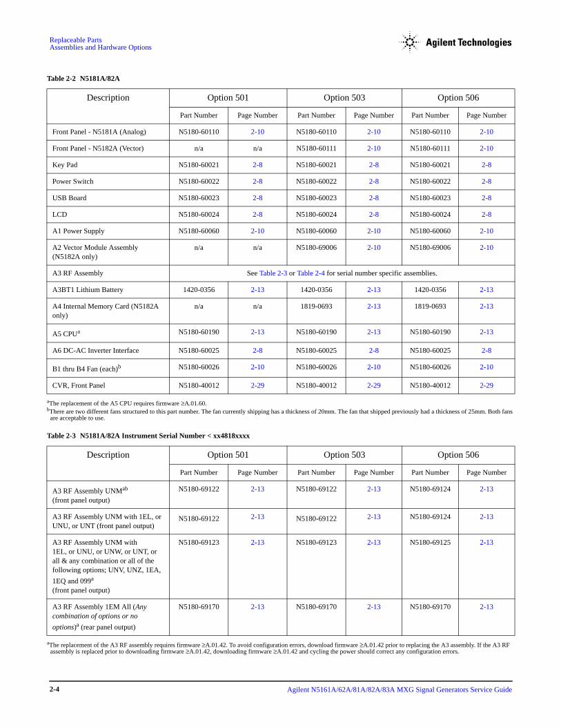
Replaceable Parts Assemblies and Hardware Options
Table 2-2 N5181A/82A
Description Option 501 Option 503 Option 506
Part Number Page Number Part Number Page Number Part Number Page Number
Front Panel - N5181A (Analog) N5180-60110 2-10 N5180-60110 2-10 N5180-60110 2-10
Front Panel - N5182A (Vector) n/a n/a N5180-60111 2-10 N5180-60111 2-10
Key Pad N5180-60021 2-8 N5180-60021 2-8 N5180-60021 2-8
Power Switch N5180-60022 2-8 N5180-60022 2-8 N5180-60022 2-8
USB Board N5180-60023 2-8 N5180-60023 2-8 N5180-60023 2-8
LCD N5180-60024 2-8 N5180-60024 2-8 N5180-60024 2-8
A1 Power Supply N5180-60060 2-10 N5180-60060 2-10 N5180-60060 2-10
A2 Vector Module Assembly (N5182A only)
n/a n/a N5180-69006 2-10 N5180-69006 2-10
A3 RF Assembly See Table 2-3 or Table 2-4 for serial number specific assemblies.
A3BT1 Lithium Battery 1420-0356 2-13 1420-0356 2-13 1420-0356 2-13
A4 Internal Memory Card (N5182A only)
n/a n/a 1819-0693 2-13 1819-0693 2-13
A5 CPUa
aThe replacement of the A5 CPU requires firmware ≥A.01.60.
N5180-60190 2-13 N5180-60190 2-13 N5180-60190 2-13
A6 DC-AC Inverter Interface N5180-60025 2-8 N5180-60025 2-8 N5180-60025 2-8
B1 thru B4 Fan (each)b
bThere are two different fans structured to this part number. The fan currently shipping has a thickness of 20mm. The fan that shipped previously had a thickness of 25mm. Both fans are acceptable to use.
N5180-60026 2-10 N5180-60026 2-10 N5180-60026 2-10
CVR, Front Panel N5180-40012 2-29 N5180-40012 2-29 N5180-40012 2-29
Table 2-3 N5181A/82A Instrument Serial Number < xx4818xxxx
Description Option 501 Option 503 Option 506
Part Number Page Number Part Number Page Number Part Number Page Number
A3 RF Assembly UNMab (front panel output)
aThe replacement of the A3 RF assembly requires firmware ≥A.01.42. To avoid configuration errors, download firmware ≥A.01.42 prior to replacing the A3 assembly. If the A3 RF assembly is replaced prior to downloading firmware ≥A.01.42, downloading firmware ≥A.01.42 and cycling the power should correct any configuration errors.
N5180-69122 2-13 N5180-69122 2-13 N5180-69124 2-13
A3 RF Assembly UNM with 1EL, or UNU, or UNT (front panel output)
N5180-69122 2-13 N5180-69122 2-13 N5180-69124 2-13
A3 RF Assembly UNM with 1EL, or UNU, or UNW, or UNT, or all & any combination or all of the following options; UNV, UNZ, 1EA,
1EQ and 099a (front panel output)
N5180-69123 2-13 N5180-69123 2-13 N5180-69125 2-13
A3 RF Assembly 1EM All (Any combination of options or no options)a (rear panel output)
N5180-69170 2-13 N5180-69170 2-13 N5180-69170 2-13
Agilent N5161A/62A/81A/82A/83A MXG Signal Generators Service Guide2-4

Replaceable Parts Assemblies and Hardware Options
bThe replacement of the A5 CPU requires firmware ≥A.01.60.
Table 2-4 N5181A/82A Instrument Serial Number > xx4818xxxx
Description Option 501 Option 503 Option 506
Part Number Page Number Part Number Page Number Part Number Page Number
A3 RF Assembly UNMa (front panel output)
N5180-69166 2-13 N5180-69166 2-13 N5180-69168 2-13
A3 RF Assembly UNM with 1EL, or UNU, or UNT (front panel output)
N5180-69166 2-13 N5180-69166 2-13 N5180-69168 2-13
A3 RF Assembly UNM with 1EL, or UNU, or UNW, or UNT, or all & any combination or all of the following options; UNV, UNZ, 1EA,
1EQ and 099a (front panel output)
N5180-69167 2-13 N5180-69167 2-13 N5180-69169 2-13
A3 RF Assembly 1EM All (Any combination of options or no options)a (rear panel output)
N5180-69170 2-13 N5180-69170 2-13 N5180-69170 2-13
aThe replacement of the A3 RF assembly requires firmware ≥A.01.42. To avoid configuration errors, download firmware ≥A.01.42 prior to replacing the A3 assembly. If the A3 RF assembly is replaced prior to downloading firmware ≥A.01.42, downloading firmware ≥A.01.42 and cycling the power should correct any configuration errors.
Table 2-5 N5183A
Description Option 520 Option 532 Option 540
Part Number Page Number Part Number Page Number Part Number Page Number
Front Panel N5180-60112 2-10 N5180-60112 2-10 N5180-60112 2-10
Key Pad N5180-60021 2-8 N5180-60021 2-8 N5180-60021 2-8
Power Switch N5180-60022 2-8 N5180-60022 2-8 N5180-60022 2-8
USB Board N5180-60023 2-8 N5180-60023 2-8 N5180-60023 2-8
LCD N5180-60024 2-8 N5180-60024 2-8 N5180-60024 2-8
A1 Power Supply N5180-60060 2-10 N5180-60060 2-10 N5180-60060 2-10
A3 RF Assembly N5180-69077 2-13 N5180-69077 2-13 N5180-69077 2-13
A3BT1 Lithium Battery 1420-0356 2-13 1420-0356 2-13 1420-0356 2-13
A5 CPUa N5180-60190 2-13 N5180-60190 2-13 N5180-60190 2-13
A6 DC-AC Inverter Interface N5180-60025 2-8 N5180-60025 2-8 N5180-60025 2-8
A7 Micro-Deck - Option UNM (front panel output)
N5180-69041 2-11 N5180-69043 2-11 N5180-69043 2-11
A7 Micro-Deck - Option 1EM (rear panel output) 3.5mm RF Connector
N5180-69042 2-11 n/a n/a n/a n/a
A7 Micro-Deck - Option 1EM (rear panel output) 2.4mm RF Connector
n/a n/a N5180-69044 2-11 N5180-69044 2-11
A7 Micro-Deck - Option 1EM (rear panel output) Type N RF Connector
N5180-69121 2-11 n/a n/a n/a n/a
Agilent N5161A/62A/81A/82A/83A MXG Signal Generators Service Guide 2-5

Replaceable Parts Assemblies and Hardware Options
A8 BNC Bypass Board E8251-63665 2-11 E8251-60061 2-11 E8251-60061 2-11
B1 thru B4 Fan (each)b N5180-60026 2-11 N5180-60026 2-11 N5180-60026 2-11
CVR, Front Panel N5180-40012 2-29 N5180-40012 2-29 N5180-40012 2-29
RF Output Connector (2.4mm) n/a n/a n/a n/a 5063-1700 n/a
RF Output Connector (Type N) 08559-60002 n/a 08559-60002 n/a n/a n/a
RF Output Connector (3.5mm) 08673-60040 n/a 08673-60040 n/a n/a n/a
aThe replacement of the A5 CPU requires firmware ≥A.01.60.bThere are two different fans structured to this part number. The fan currently shipping has a thickness of 20mm. The fan that shipped previously had a thickness of 25mm. Both fans
are acceptable to use.
Table 2-5 N5183A
Agilent N5161A/62A/81A/82A/83A MXG Signal Generators Service Guide2-6

Replaceable Parts Assemblies and Hardware Options
Front Panel Assemblies (N5161A/62A only)
Figure 2-1 Front Panel Assemblies
USB Board Power SwitchA9 Interface Board
Agilent N5161A/62A/81A/82A/83A MXG Signal Generators Service Guide 2-7

Replaceable Parts Assemblies and Hardware Options
Front Panel Assemblies (N5181A/82A/83A only)
Figure 2-2 Front Panel Assemblies
Key Pad
USB Board
Power Switch
A6 DC-AC Inverter Interface
LCD
Agilent N5161A/62A/81A/82A/83A MXG Signal Generators Service Guide2-8

Replaceable Parts Assemblies and Hardware Options
Assemblies from a Top View
Figure 2-3 N5161A and N5162A (Option 012 Shown)
A1 A2 (N5162A only)
B1 B2 B3 B4Front Panel
Agilent N5161A/62A/81A/82A/83A MXG Signal Generators Service Guide 2-9

Replaceable Parts Assemblies and Hardware Options
Figure 2-4 N5181A/82A
A1 A2 (N5182A only)
B1 B2 B3 B4Front Panel
Agilent N5161A/62A/81A/82A/83A MXG Signal Generators Service Guide2-10
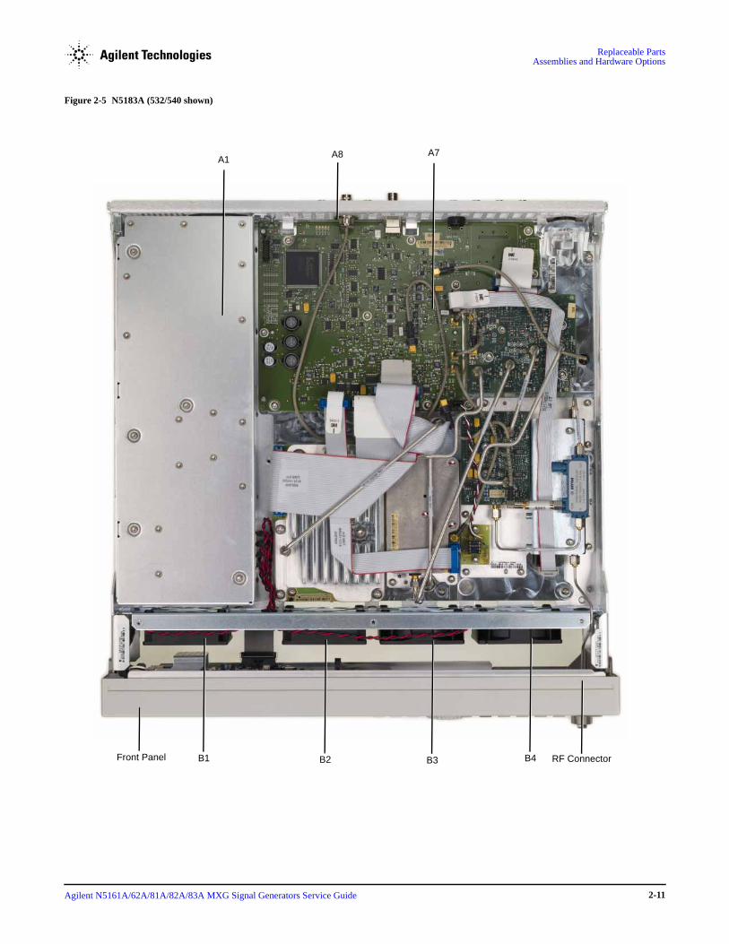
Replaceable Parts Assemblies and Hardware Options
Figure 2-5 N5183A (532/540 shown)
A1
B1 B2 B3 B4Front Panel
A7A8
RF Connector
Agilent N5161A/62A/81A/82A/83A MXG Signal Generators Service Guide 2-11
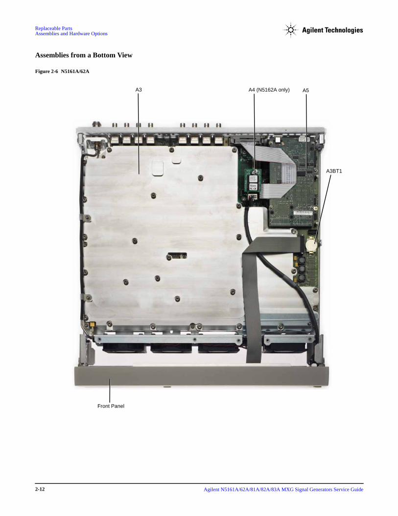
Replaceable Parts Assemblies and Hardware Options
Assemblies from a Bottom View
Figure 2-6 N5161A/62A
A3 A5
A3BT1
A4 (N5162A only)
Front Panel
Agilent N5161A/62A/81A/82A/83A MXG Signal Generators Service Guide2-12

Replaceable Parts Assemblies and Hardware Options
Figure 2-7 N5181A/82A/83A
A3 A5
A3BT1
A4 (N5182A only)
Agilent N5161A/62A/81A/82A/83A MXG Signal Generators Service Guide 2-13

Replaceable Parts Assemblies and Hardware Options
CablesThis section lists part numbers for the cables in your signal generator.
Table 2-6
Reference Designator
Input Output Part Number Page Number
B1W1a Wire Cable, B1 Fan A1 Power Supply (part of B1) 2-16 & 2-17
B2W1a Wire Cable, B2 Fan A1 Power Supply (part of B2) 2-16 & 2-17
B3W1a Wire Cable, B3 Fan A1 Power Supply (part of B3) 2-16 & 2-17
B4W1a Wire Cable, B4 Fan A1 Power Supply (part of B4) 2-16 & 2-17
W1 Ribbon Cable, Front Panel A3 RF Assembly 8121-1398 2-19 & 2-20
W2 Front Panel (USB) A3 RF Assembly 8121-1396 2-19 & 2-20
W3(N5182A only)
Front Panel (I Input) A2J15 8121-0642 2-16 & 2-17
W4(N5182A only)
Front Panel (Q Input) A2J16 8121-0642 2-16 & 2-17
W5(N5182A only)
Semi-Rigid Cable, A3 RF Assembly A2 Vector Modulation N5180-20016 2-17
W6(N5182A only)
Semi-Rigid Cable, A3 RF Assembly A2 Vector Modulation N5180-20025 2-17
W7(N5162A/82A
only)
Semi-Rigid Cable, A3 RF Assembly A2 Vector Modulation N5180-20026 2-16 & 2-17
W8 Ribbon Cable, A3 RF Assembly (GPIB) A5 CPU 8121-1397 2-19 & 2-20
W9(N5183A only)
Semi-Rigid Cable, 2.4mm RF Connector Mechanical Attenuator N5180-20046 2-18
W10(N5183A only)
Semi-Rigid Cable, 3.5mm RF Connector Mechanical Attenuator N5180-20057 2-18
W11(N5183A only)
Semi-Rigid Cable, Type-N RF Connector Mechanical Attenuator N5180-20088 2-18
W12(N5183A only)
Semi-Rigid Cable, A3 RF Assembly A7 Micro Desk Low Band Coupler N5180-20040 2-18
W13(N5183A only)
Semi-Rigid Cable, A3 RF Assembly A7 Micro Deck 20 GHz Doubler N5180-20039 2-18
W14(N5183A only)
A7J15 A3 RF Assembly 8121-1578 2-18
W15(N5183A only)
A7J14 Rear Panel (ALC Input) 8121-0859 2-18
W16(N5162A/82A
Option 012 only)
Semi-Rigid Cable, LO In Rear Panel N5180-20140 2-16
Agilent N5161A/62A/81A/82A/83A MXG Signal Generators Service Guide2-14
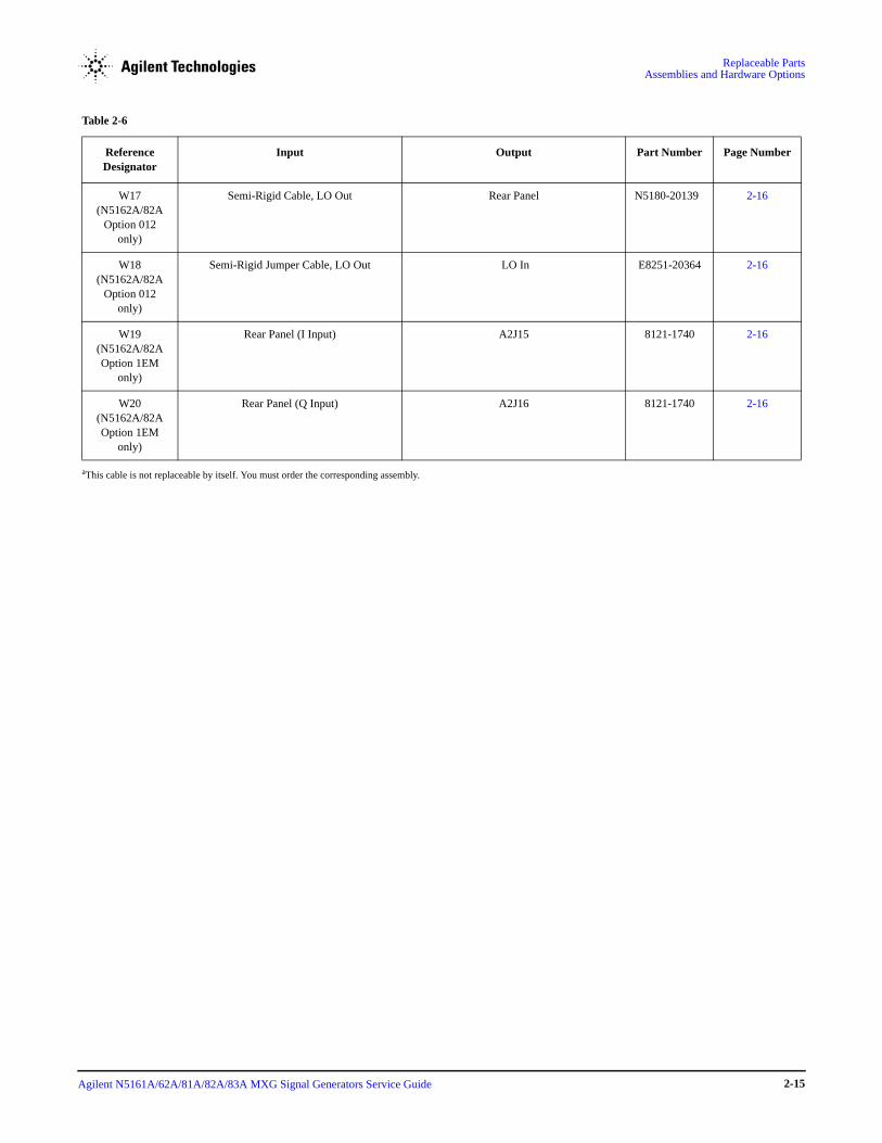
Replaceable Parts Assemblies and Hardware Options
W17(N5162A/82A
Option 012 only)
Semi-Rigid Cable, LO Out Rear Panel N5180-20139 2-16
W18(N5162A/82A
Option 012 only)
Semi-Rigid Jumper Cable, LO Out LO In E8251-20364 2-16
W19 (N5162A/82A Option 1EM
only)
Rear Panel (I Input) A2J15 8121-1740 2-16
W20 (N5162A/82A Option 1EM
only)
Rear Panel (Q Input) A2J16 8121-1740 2-16
aThis cable is not replaceable by itself. You must order the corresponding assembly.
Table 2-6
Reference Designator
Input Output Part Number Page Number
Agilent N5161A/62A/81A/82A/83A MXG Signal Generators Service Guide 2-15

Replaceable Parts Assemblies and Hardware Options
Cables from a Top View
Figure 2-8 N5162A with Option 012 and N5182A with Options 1EM and 012
W18W17 W7W16
B1W1 B2W1 B3W1 B4W1
W20 W19
Agilent N5161A/62A/81A/82A/83A MXG Signal Generators Service Guide2-16

Replaceable Parts Assemblies and Hardware Options
Figure 2-9 N5181A/82A
W5 W6 W7W4 W3
B1W1 B2W1 B3W1 B4W1
Agilent N5161A/62A/81A/82A/83A MXG Signal Generators Service Guide 2-17

Replaceable Parts Assemblies and Hardware Options
Figure 2-10N5183A
W15 W14
2.4mm - W93.5mm - W10Type-N - W11
W13 W12
Agilent N5161A/62A/81A/82A/83A MXG Signal Generators Service Guide2-18

Replaceable Parts Assemblies and Hardware Options
Cables from a Bottom View
Figure 2-11N5161A/62A
W8
W1 W2
Agilent N5161A/62A/81A/82A/83A MXG Signal Generators Service Guide 2-19

Replaceable Parts Assemblies and Hardware Options
Figure 2-12N5181A/82A/83A
W8
W1 W2
Agilent N5161A/62A/81A/82A/83A MXG Signal Generators Service Guide2-20

Replaceable Parts Assemblies and Hardware Options
Hardware This section lists part numbers for hardware and other instrument parts in your signal generator.
• “Front Panel View” on page 2-21
• “Disassembled Rear Panel View” on page 2-23
• “Main Chassis with Inside Covers” on page 2-26
• “Outer Instrument Cover and Associated Parts” on page 2-27
Front Panel ViewTable 2-7 Front Panel View
Item No. Description Qty Part Number
1 Small Overlay 1 N/A
2 Nameplate 1 N/A
3 RPG Knob 1 W1312-40017
4 Large Keypad Overlay 1 N/A
5 Washer-Wavy .490ID (N5182A only) 2 2190-0102
6 Nut-Hex 15/32-32 (N5182A only) 2 2950-0035
7 Front Panel Overlay (N5161A/62A only) 1 N/A
Agilent N5161A/62A/81A/82A/83A MXG Signal Generators Service Guide 2-21

Replaceable Parts Assemblies and Hardware Options
Figure 2-13N5161A/62A Front Panel View
Figure 2-14N5181A/83A Front Panel View
Figure 2-15N5182A Front Panel View
7
13 4
2
1 3 4
5 6
2
Agilent N5161A/62A/81A/82A/83A MXG Signal Generators Service Guide2-22

Replaceable Parts Assemblies and Hardware Options
Disassembled Rear Panel ViewTable 2-8 Disassembled Rear Panel View
Item No. Description Qty Part Number
1 Rear Panel - N5161A/81A Rear Panel - N5162A/82A Rear Panel - N5183A
111
N5180-00002N5180-00017N5180-00006
2 Screw-Machine M3.0 8 -PN-TX N5161A/81A N5162A/82A N5183A
41010
0515-0372
3 Screw-Machine 4-40 (N5162A/82A only) 4 2200-0139
4 Washer Lock .505ID (BNC connectors on rear-panel) N5161A/81A N5162A/82A N5183A
8159
2190-0068
5 Nut-Hex 1/2-28 (BNC connectors on rear-panel board) N5161A/81A N5162A/82A N5183A
8159
2950-0054
6 Rear-Panel Hole Plug 1 6960-0517
7 Rear-Panel BNC Hole Plug (N5183A only) 1 N/A
Agilent N5161A/62A/81A/82A/83A MXG Signal Generators Service Guide 2-23
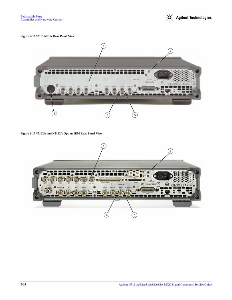
Replaceable Parts Assemblies and Hardware Options
Figure 2-16N5161A/81A Rear Panel View
Figure 2-17N5162A and N5182A Option 1EM Rear Panel View
1
2
46 5
1
2
4 5
Agilent N5161A/62A/81A/82A/83A MXG Signal Generators Service Guide2-24
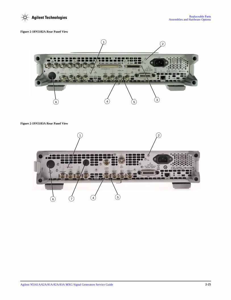
Replaceable Parts Assemblies and Hardware Options
Figure 2-18N5182A Rear Panel View
Figure 2-19N5183A Rear Panel View
12
46 53
1 2
4657
Agilent N5161A/62A/81A/82A/83A MXG Signal Generators Service Guide 2-25
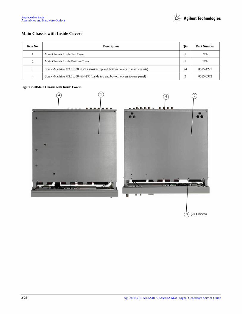
Replaceable Parts Assemblies and Hardware Options
Main Chassis with Inside Covers
Figure 2-20Main Chassis with Inside Covers
Table 2-9 Main Chassis with Inside Covers
Item No. Description Qty Part Number
1 Main Chassis Inside Top Cover 1 N/A
2 Main Chassis Inside Bottom Cover 1 N/A
3 Screw-Machine M3.0 x 08 FL-TX (inside top and bottom covers to main chassis) 24 0515-1227
4 Screw-Machine M3.0 x 08 -PN-TX (inside top and bottom covers to rear panel) 2 0515-0372
1 244
3 (24 Places)
Agilent N5161A/62A/81A/82A/83A MXG Signal Generators Service Guide2-26

Replaceable Parts Assemblies and Hardware Options
Outer Instrument Cover and Associated PartsTable 2-10Outer Instrument Cover and Associated Parts
Item No. Description Qty Part Number
1 Assy-Strap Handle - includes the following parts: 1 E4400-60026
Strap Assembly 1
Ground Spring 2
Handle Retainer 2
End Cap 2
Screw-Machine M5 x 18 FL-TX 2
2 Hole Plug (not shown in photo) 2 W1312-40024
3 Screw-Machine M5 x 0.8 12mm-lg (not shown in photo) 2 0515-0708
4 Rear Feet Screws (not shown in photo) 4 0515-1619
5 Rear-Panel Feet 4 5041-9611
6 Feet-Bottom 1 5041-9167
7 Tilt Stand 1 1460-1345
8 Set of 4 Bottom Feet with Tilt Stands (not shown in photo) 1 5000-0913
9 Outside Instrument Cover 1 W1312-00018
10 Hole Plug, Bottom Feet (not shown in photo) 1 W1312-40032
11 Front Panel Cover 1 N5180-40012
Agilent N5161A/62A/81A/82A/83A MXG Signal Generators Service Guide 2-27

Replaceable Parts Assemblies and Hardware Options
Figure 2-21Outer Instrument Cover and Associated Parts
1
5(4 Places)
6(4 Places)
9
7 (2 Places)
Agilent N5161A/62A/81A/82A/83A MXG Signal Generators Service Guide2-28

Replaceable Parts Assemblies and Hardware Options
Figure 2-22 Front Panel Cover
MiscellaneousThis section lists part numbers for miscellaneous items that can be used with your signal generator.
Documentation
NOTE The N516xA/8xA MXG documentation can also be found on the web at http://www.agilent.com/find/mxg.
Electrostatic Discharge (ESD) Protective Supplies
Table 2-11Documentation
Description Part Number
Documentation Set N5180-90001
CD-ROM Documentation N5180-90007
Installation Guide N5180-90002
User’s Guide N5180-90003
SCPI Command Reference N5180-90004
Programming Guide N5180-90005
Service Guide N5180-90006
Specifications/Data Sheet (N5161A/81A) 5989-5311EN
Specifications/Data Sheet (N5162A/82A) 5989-5261EN
Specifications/Data Sheet (N5183A) 5989-7572EN
Table 2-12Electrostatic Discharge (ESD) Protective Supplies
Description Part Number
ESD connector end cap front-panel RF output 1401-0247
ESD connector end cap-GPIB 1252-5007
2 X 4 Ft. Antistatic Table Mat with 15 FT. Ground Wire 9300-0797
5 Ft. Grounding Cord (for wrist strap) 9300-0980
Adjustable Antistatic Wrist Strap 9300-1367
11
Agilent N5161A/62A/81A/82A/83A MXG Signal Generators Service Guide 2-29
Replaceable Parts Assemblies and Hardware Options
Abbreviations Used in Part DescriptionsThis section defines the reference designators, abbreviations, and option numbers that are used in the part descriptions throughout this chapter.
Reference Designator
Definition
A assembly
AT attenuator
B fan
DS lamp
J electrical connector; jack
W cable; transmission path; wire
Abbreviation Definition
BN buttonhead (screws)
CPU central processing unit
conical washer (screws)
EXT external
FL flathead (screws)
Ft feet
Hex hexagonal
GPIB general purpose interface bus
HX hexagonal recess (screws)
I in-phase
LF low frequency
M meters or metric hardware
PC patch lock (screws) or printed circuit
PN panhead (screws)
Q quadrature
Qty quantity
RF radio frequency
RPP reverse power protection
SMA subminiature type-A
TX TORX recess (screws)
Agilent N5161A/62A/81A/82A/83A MXG Signal Generators Service Guide2-30

3 Assembly Replacement
Before You Replace an Assembly
CAUTION Many of the assemblies in this instrument are very susceptible to damage from electrostatic discharge (ESD). Perform service procedures only at a static-safe workstation and wear a grounding strap.
You must upgrade your firmware, to at least A.01.10, before replacing any assembly. Go to www.agilent.com/find/upgradeassistant for information on upgrading you firmware.
To avoid internal calibration failures and potential post-repair errors, before removing any instrument assembly, the instrument’s static and dynamic arrays must be configured for the exchange of assemblies. The process to do the appropriate configuration is performed automatically by the MXG with the Assembly Installation and Removal Overview front panel softkeys. Refer to the Assembly Installation and Removal Overview and to the ”Hardware Assembly Installation and Removal Softkeys” on page 4-2.
Be sure to review the warning and caution statements described in Chapter 5, "Safety and Regulatory," on page 5-1, prior to replacing an assembly in your signal generator.
After Replacing or Repairing an AssemblyAfter you have replaced or repaired an assembly, certain performance tests may have to be performed. Refer to Chapter 4, "Post-Repair Procedures and Performance Verification," on page 4-1, for the list of performance tests required for each assembly.
Assemblies You Can Replace• ”Outer Cover” on page 3-4
• ”Inner Top Cover” on page 3-6
• ”Inner Bottom Cover” on page 3-8
• ”Front-Panel” on page 3-10
• ”USB Board” on page 3-12
• ”LCD Display (N5181A/82A/83A only)” on page 3-14
• ”A6 DC-AC Inverter Interface Board (N5181A/82A/83A only)” on page 3-16
• “A9 Interface Board (N5161A/62A only)” on page 18
• ”Key Pad (N5181A/82A/83A only)” on page 3-20
• ”Power Switch” on page 3-21
• ”Rear Panel (N5161A/81A)” on page 3-22
• ”Rear Panel (N5162A/82A)” on page 3-24
• ”Rear Panel (N5183A)” on page 3-26
• ”A1 Power Supply” on page 3-28
• “A2 Vector Module (N5162A with Option 012 and N5182A Option 1EM with Option 012)” on page 30
• ”A2 Vector Module (N5162A/82A without Option 012)” on page 3-32
• “A3 RF Assembly (N5162A, with and without Option 012, N5182A with Option 012, and N5182A Option 1EM, with and without Option 012)” on page 34
• ”A3 RF Assembly - Standard (N5181A/82A)” on page 3-38
• ”A3 RF Assembly - N5161A and N5181A Option 1EM” on page 3-42
• ”A3 RF Assembly (N5183A only)” on page 3-46
• ”A3BT1 Battery” on page 3-50
• ”A4 Internal Memory Card (N5162A/82A only)” on page 3-52
• ”A5 CPU” on page 3-54
Agilent N5161A/62A/81A/82A/83A MXG Signal Generators Service Guide 3-1

Assembly ReplacementAssemblies You Can Replace
• ”A7 Micro-Deck (N5183A only - Standard)” on page 3-56
• ”A7 Micro-Deck (N5183A only - Option 1EM)” on page 3-59
• ”A8 Floating BNC Bypass (N5183A only)” on page 3-62
• ”RF Connector (N5183A only - Standard)” on page 3-64
• ”B1 thru B4 Fans” on page 3-66
Agilent N5161A/62A/81A/82A/83A MXG Signal Generators Service Guide 3-2
Assembly Replacement Assemblies You Can Replace
This page intentionally left blank.
Agilent N5161A/62A/81A/82A/83A MXG Signal Generators Service Guide 3-3

Assembly ReplacementOuter Cover
Outer Cover
Tools Required • T-20 driver
Removal Procedure
Refer to Figure 3-1 for this procedure.
1. Disconnect the power cord.
2. Using the T-20 driver, loosen the two screws (1) and remove the strap handle (2).
3. Using the T-20 driver, remove the two hole plugs (not shown in photo) from the opposite side of the instrument.
4. Using the T-20 driver, remove the center screws from the four rear-panel feet (3).
5. Remove the four bottom feet (4) from the cover by lifting the tab and sliding the foot toward the tab.
6. Place the signal generator on its side.
7. Place one hand on the front panel, use the other hand to lift the rear of the signal generator and slide the outer cover (5) off to remove it from the frame.
CAUTION The RF connector can be easily damaged. Use extreme caution to not damage the RF connector when lifting the rear of the signal generator.
Replacement Procedure 1. Reverse the order of the removal procedures.
CAUTION When sliding the outer cover back on the signal generator keep fingers away from the back of the front panel. They can get pinched.
2. Torque all screws to 21 in–lbs.
Agilent N5161A/62A/81A/82A/83A MXG Signal Generators Service Guide 3-4

Assembly Replacement Outer Cover
Figure 3-1 Outer Cover Removal
1 2
3
(2 Places)
(4 Places)
4(4 Places)
5
Agilent N5161A/62A/81A/82A/83A MXG Signal Generators Service Guide 3-5
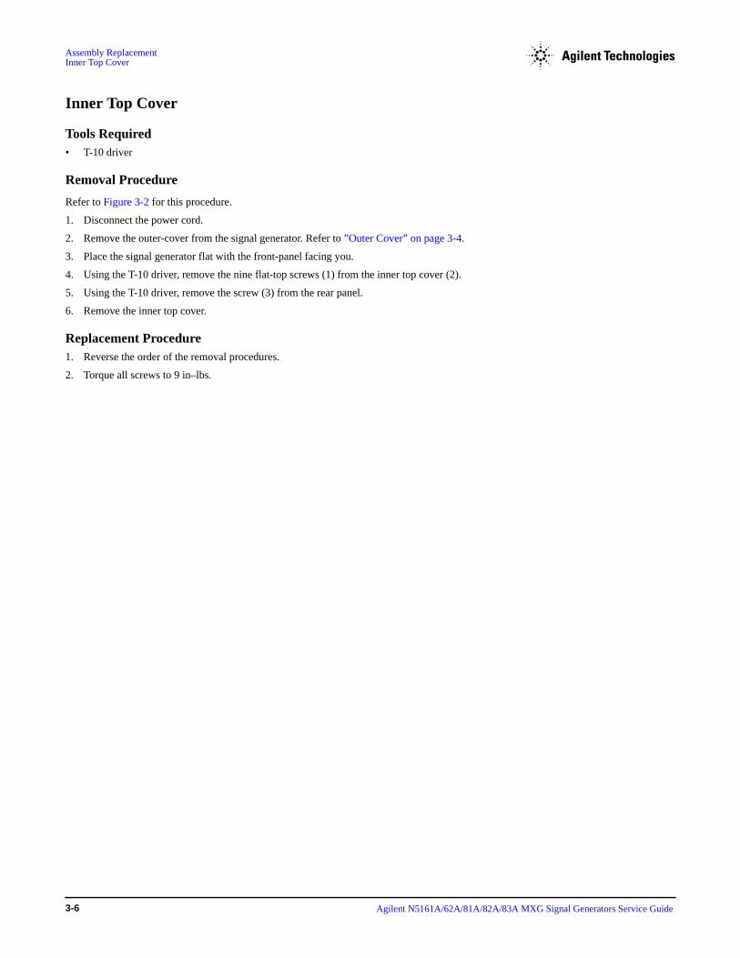
Assembly ReplacementInner Top Cover
Inner Top Cover
Tools Required • T-10 driver
Removal Procedure
Refer to Figure 3-2 for this procedure.
1. Disconnect the power cord.
2. Remove the outer-cover from the signal generator. Refer to ”Outer Cover” on page 3-4.
3. Place the signal generator flat with the front-panel facing you.
4. Using the T-10 driver, remove the nine flat-top screws (1) from the inner top cover (2).
5. Using the T-10 driver, remove the screw (3) from the rear panel.
6. Remove the inner top cover.
Replacement Procedure 1. Reverse the order of the removal procedures.
2. Torque all screws to 9 in–lbs.
Agilent N5161A/62A/81A/82A/83A MXG Signal Generators Service Guide 3-6
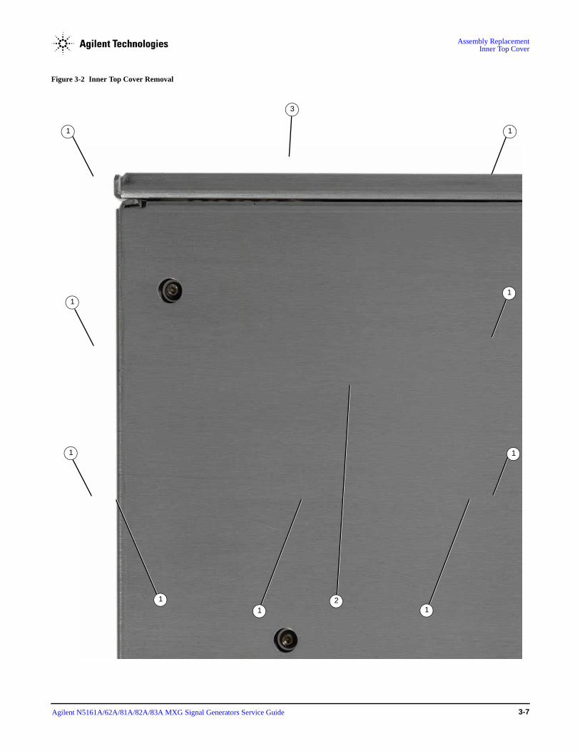
Assembly Replacement Inner Top Cover
Figure 3-2 Inner Top Cover Removal
3
211
1
1
1
1
1
1
1
Agilent N5161A/62A/81A/82A/83A MXG Signal Generators Service Guide 3-7

Assembly ReplacementInner Bottom Cover
Inner Bottom Cover
Tools Required • T-10 driver
Removal Procedure
Refer to Figure 3-3 for this procedure.
1. Disconnect the power cord.
2. Remove the outer-cover from the signal generator. Refer to ”Outer Cover” on page 3-4.
3. Place the signal generator flat with the front-panel facing you.
4. Using the T-10 driver, remove the eleven flat-top screws (1) from the inner bottom cover (2).
5. Using the T-10 driver, remove the screw (3) from the rear panel.
6. Remove the inner bottom cover.
Replacement Procedure 1. Reverse the order of the removal procedures.
2. Torque all screws to 9 in–lbs.
Agilent N5161A/62A/81A/82A/83A MXG Signal Generators Service Guide 3-8
Assembly Replacement Inner Bottom Cover
Figure 3-3 Inner Bottom Cover
3
2
1 1
11
1 1
111
Agilent N5161A/62A/81A/82A/83A MXG Signal Generators Service Guide 3-9

Assembly ReplacementFront-Panel
Front-Panel
Tools Required • T-20 driver
• needle-nose pliers
Removal Procedure
Refer to Figure 3-4 for this procedure.
1. Disconnect the power cord.
2. Remove the covers from the signal generator. Refer to ”Outer Cover” on page 3-4, ”Inner Top Cover” on page 3-6, and ”Inner Bottom Cover” on page 3-8.
3. With the signal generator on its side, disconnect W1 and W2 from the A3 RF assembly by squeezing the cable connector and pulling the cable away from the signal generator.
4. Release W2 from the cable clips.
5. For N5182A instruments, place the signal generator flat with the A2 Vector Module facing you and use the needle-nose pliers to disconnect the following cables,
• W3 (I Input) from A2J15
• W4 (Q Input) from A2J16
6. Remove the chassis grommet before pulling W3 and W4 thru the chassis (N5182A only).
7. With the signal generator upside down and flat, use the T-20 driver to remove the four screws (1) from the sides of the chassis
CAUTION Before removing the front-panel from the signal generator, lift and support the front frame of the signal generator.
8. Slide the front-panel over the RF output connector (N5181A/82A/83A standard models only).
9. Remove the front-panel.
Replacement Procedure 1. Reverse the order of the removal procedure.
2. Torque all screws to 21 in–lbs.
3. Perform the post-repair performance tests that pertain to this replacement procedure, see Chapter 4, Post-Repair Procedures and Performance Verification.
Agilent N5161A/62A/81A/82A/83A MXG Signal Generators Service Guide 3-10

Assembly Replacement Front-Panel
Figure 3-4 Front-Panel
W1
1
W3/A2J15
W2
1
2 places2 places
W4/A2J16(N5182A only) (N5182A only)
chassisgrommet
Agilent N5161A/62A/81A/82A/83A MXG Signal Generators Service Guide 3-11
Assembly ReplacementUSB Board
USB Board
Tools Required • T-10 driver
Removal Procedure
Refer to Figure 3-5 for this procedure.
1. Disconnect the power cord.
2. Remove the covers from the signal generator. Refer to ”Outer Cover” on page 3-4, ”Inner Top Cover” on page 3-6, and ”Inner Bottom Cover” on page 3-8.
3. Remove the front-panel from the signal generator. Refer to ”Front-Panel” on page 3-10.
4. Using the T-10 driver, remove the screw (1) securing the USB board to the front-panel.
5. Remove USB board
Replacement Procedure 1. Reverse the order of the removal procedure.
2. Torque screw to 9 in–lbs.
3. Perform the post-repair performance tests that pertain to this replacement procedure, see Chapter 4, Post-Repair Procedures and Performance Verification.
Agilent N5161A/62A/81A/82A/83A MXG Signal Generators Service Guide 3-12

Assembly Replacement USB Board
Figure 3-5 USB Board
1
Agilent N5161A/62A/81A/82A/83A MXG Signal Generators Service Guide 3-13

Assembly ReplacementLCD Display (N5181A/82A/83A only)
LCD Display (N5181A/82A/83A only)
Tools Required • T-10 driver
Removal Procedure
Refer to Figure 3-6 for this procedure.
1. Disconnect the power cord.
2. Remove the covers from the signal generator. Refer to ”Outer Cover” on page 3-4, ”Inner Top Cover” on page 3-6, and ”Inner Bottom Cover” on page 3-8.
3. Remove the front-panel from the signal generator. Refer to ”Front-Panel” on page 3-10.
4. Remove the A6 DC-AC Inverter Interface Board from the signal generator. Refer to ”A6 DC-AC Inverter Interface Board (N5181A/82A/83A only)” on page 3-16.
5. Using the T-10 driver, remove the six screws (1) that secure the sub-panel (2) to the front-panel.
6. Remove the sub-panel.
7. Remove the LCD Display.
Replacement Procedure 1. Reverse the order of the removal procedure.
2. Torque all screws to 9 in–lbs.
3. Perform the post-repair performance tests that pertain to this replacement procedure, see Chapter 4, Post-Repair Procedures and Performance Verification.
Agilent N5161A/62A/81A/82A/83A MXG Signal Generators Service Guide 3-14

Assembly Replacement LCD Display (N5181A/82A/83A only)
Figure 3-6 LCD Display
1 1 1 1
11
2
LCD Display
Agilent N5161A/62A/81A/82A/83A MXG Signal Generators Service Guide 3-15
Assembly ReplacementA6 DC-AC Inverter Interface Board (N5181A/82A/83A only)
A6 DC-AC Inverter Interface Board (N5181A/82A/83A only)
Tools Required • T-10 driver
Removal Procedure
Refer to Figure 3-7 for this procedure.
1. Disconnect the power cord.
2. Remove the covers from the signal generator. Refer to ”Outer Cover” on page 3-4, ”Inner Top Cover” on page 3-6, and ”Inner Bottom Cover” on page 3-8.
3. Remove the front-panel from the signal generator. Refer to ”Front-Panel” on page 3-10.
4. Using the T-10 driver, remove the four screws (1) that secure the inverter shield (2) to the A6 DC-AC Inverter Interface Board (3).
5. Disconnect the W1 ribbon cable (not shown in Figure 3-7) from the A6 DC-AC Inverter Interface board (3).
6. Disconnect the Power Switch cable (4) from the A6 DC-AC Inverter Interface Board (3).
7. Disconnect the LCD 2 wire cable (5) from the A6 DC-AC Inverter Interface Board (3).
8. Disconnect the ribbon cable (6) from the A6 DC-AC Inverter Interface Board (3).
9. Disconnect the LCD flat flex cable (7) from the A6 DC-AC Inverter Interface Board (3).
10. Using the T-10 driver, remove the three screws (8) that secure the A6 DC-AC Inverter Interface Board (3) to the front-panel sub-panel (9).
11. Remove the A6 DC-AC Inverter Interface Board.
Replacement Procedure 1. Reverse the order of the removal procedure.
2. Torque all screws to 9 in–lbs.
3. Perform the post-repair performance tests that pertain to this replacement procedure, see Chapter 4, Post-Repair Procedures and Performance Verification.
Agilent N5161A/62A/81A/82A/83A MXG Signal Generators Service Guide 3-16

Assembly Replacement A6 DC-AC Inverter Interface Board (N5181A/82A/83A only)
Figure 3-7 A6 DC-AC Inverter Interface Board
1 1
11
2
3
4
5
3
6
7
8
8 89
Agilent N5161A/62A/81A/82A/83A MXG Signal Generators Service Guide 3-17
Assembly ReplacementA9 Interface Board (N5161A/62A only)
A9 Interface Board (N5161A/62A only)
Tools Required • T-10 driver
Removal Procedure
Refer to Figure 3-8 for this procedure.
1. Disconnect the power cord.
2. Remove the covers from the signal generator. Refer to ”Outer Cover” on page 3-4, ”Inner Top Cover” on page 3-6, and ”Inner Bottom Cover” on page 3-8.
3. Remove the front-panel from the signal generator. Refer to ”Front-Panel” on page 3-10.
4. Disconnect the W1 ribbon cable from the A9 Interface board (3).
5. Using the T-10 driver, remove the six screws (1) that secure the subpanel (2) to the front panel (3).
6. Disconnect the Power Switch cable (4) from the A9 Interface Board (3).
7. Using the T-10 driver, remove the seven screws (5) that secure the A9 Interface Board (3) to the front-panel sub-panel (6).
8. Remove the A9 Interface Board.
Replacement Procedure 1. Reverse the order of the removal procedure.
2. Torque all screws to 9 in–lbs.
3. Perform the post-repair performance tests that pertain to this replacement procedure, see Chapter 4, Post-Repair Procedures and Performance Verification.
Agilent N5161A/62A/81A/82A/83A MXG Signal Generators Service Guide 3-18

Assembly Replacement A9 Interface Board (N5161A/62A only)
Figure 3-8 A9 Interface Board
1 1
1
1
2
5
4
3
5
5 5
1 1
6
5
5
5
W1
Agilent N5161A/62A/81A/82A/83A MXG Signal Generators Service Guide 3-19
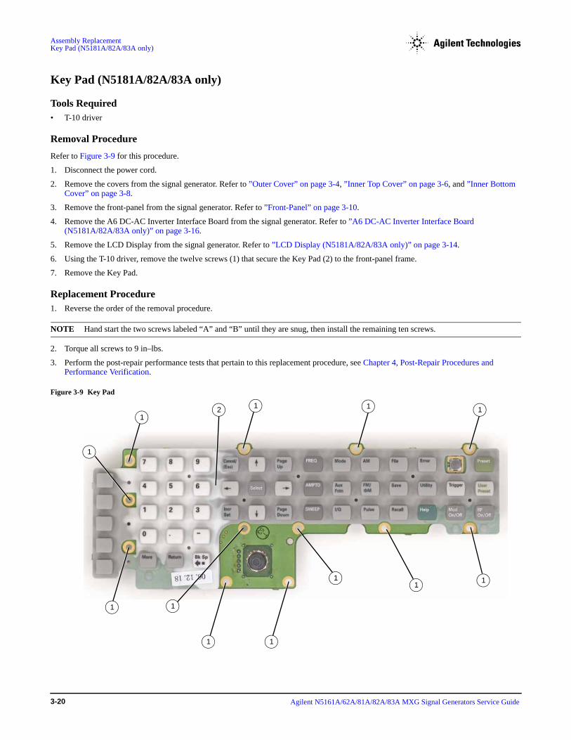
Assembly ReplacementKey Pad (N5181A/82A/83A only)
Key Pad (N5181A/82A/83A only)
Tools Required • T-10 driver
Removal Procedure
Refer to Figure 3-9 for this procedure.
1. Disconnect the power cord.
2. Remove the covers from the signal generator. Refer to ”Outer Cover” on page 3-4, ”Inner Top Cover” on page 3-6, and ”Inner Bottom Cover” on page 3-8.
3. Remove the front-panel from the signal generator. Refer to ”Front-Panel” on page 3-10.
4. Remove the A6 DC-AC Inverter Interface Board from the signal generator. Refer to ”A6 DC-AC Inverter Interface Board (N5181A/82A/83A only)” on page 3-16.
5. Remove the LCD Display from the signal generator. Refer to ”LCD Display (N5181A/82A/83A only)” on page 3-14.
6. Using the T-10 driver, remove the twelve screws (1) that secure the Key Pad (2) to the front-panel frame.
7. Remove the Key Pad.
Replacement Procedure 1. Reverse the order of the removal procedure.
NOTE Hand start the two screws labeled “A” and “B” until they are snug, then install the remaining ten screws.
2. Torque all screws to 9 in–lbs.
3. Perform the post-repair performance tests that pertain to this replacement procedure, see Chapter 4, Post-Repair Procedures and Performance Verification.
Figure 3-9 Key Pad
1
1
1 1
11
1
11
11
1
2
Agilent N5161A/62A/81A/82A/83A MXG Signal Generators Service Guide 3-20
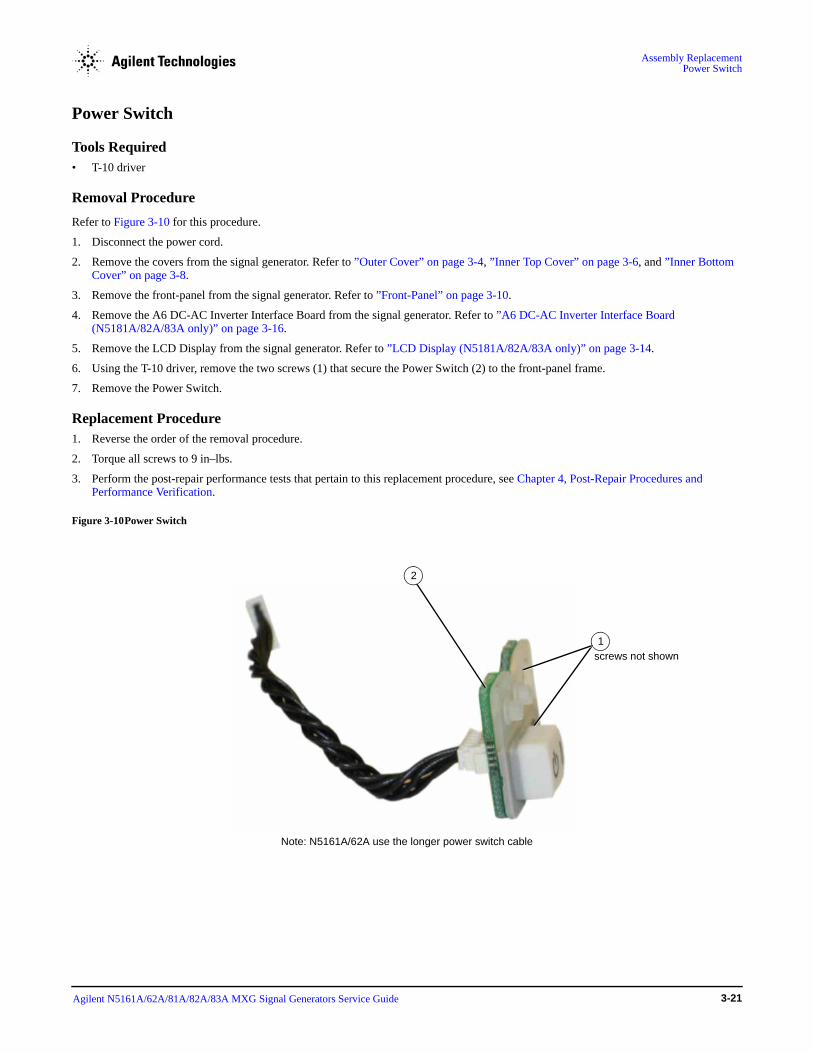
Assembly Replacement Power Switch
Power Switch
Tools Required • T-10 driver
Removal Procedure
Refer to Figure 3-10 for this procedure.
1. Disconnect the power cord.
2. Remove the covers from the signal generator. Refer to ”Outer Cover” on page 3-4, ”Inner Top Cover” on page 3-6, and ”Inner Bottom Cover” on page 3-8.
3. Remove the front-panel from the signal generator. Refer to ”Front-Panel” on page 3-10.
4. Remove the A6 DC-AC Inverter Interface Board from the signal generator. Refer to ”A6 DC-AC Inverter Interface Board (N5181A/82A/83A only)” on page 3-16.
5. Remove the LCD Display from the signal generator. Refer to ”LCD Display (N5181A/82A/83A only)” on page 3-14.
6. Using the T-10 driver, remove the two screws (1) that secure the Power Switch (2) to the front-panel frame.
7. Remove the Power Switch.
Replacement Procedure 1. Reverse the order of the removal procedure.
2. Torque all screws to 9 in–lbs.
3. Perform the post-repair performance tests that pertain to this replacement procedure, see Chapter 4, Post-Repair Procedures and Performance Verification.
Figure 3-10Power Switch
1
2
screws not shown
Note: N5161A/62A use the longer power switch cable
Agilent N5161A/62A/81A/82A/83A MXG Signal Generators Service Guide 3-21

Assembly ReplacementRear Panel (N5161A/81A)
Rear Panel (N5161A/81A)
Tools Required • T-10 driver
• 5/8” hex-nut driver
Removal Procedure
Refer to Figure 3-11 for this procedure.
1. Disconnect the power cord.
2. Remove the covers from the signal generator. Refer to ”Outer Cover” on page 3-4, ”Inner Top Cover” on page 3-6, and ”Inner Bottom Cover” on page 3-8.
3. Place the signal generator flat with the rear panel facing you.
4. Using the 5/8” hex-nut driver, remove the nuts and washers (1) securing the A3 RF assembly BNC’s to the rear panel.
5. Using the T-10 driver, remove the four screws (2) securing the rear panel to the signal generators chassis.
6. Pull the rear panel away from the signal generator’s chassis.
Replacement Procedure 1. Reverse the order of the removal procedure.
2. Torque all screws to 9 in–lbs.
3. Torque all BNC connectors to 8 in–lbs.
4. Perform the post-repair performance tests that pertain to this replacement procedure, see Chapter 4, Post-Repair Procedures and Performance Verification.
Agilent N5161A/62A/81A/82A/83A MXG Signal Generators Service Guide 3-22

Assembly Replacement Rear Panel (N5161A/81A)
Figure 3-11N5161A/81A Disassembled Rear Panel View
2
1
Agilent N5161A/62A/81A/82A/83A MXG Signal Generators Service Guide 3-23
Assembly ReplacementRear Panel (N5162A/82A)
Rear Panel (N5162A/82A)
Tools Required • T-10 driver
• 5/8” hex-nut driver
• 5/16” open-ended wrench
• 1/4” hex-nut driver
• small Phillips screwdriver
Removal Procedure
Refer to Figure 3-12 for this procedure.
1. Disconnect the power cord.
2. Remove the covers from the signal generator. Refer to ”Outer Cover” on page 3-4, ”Inner Top Cover” on page 3-6, and ”Inner Bottom Cover” on page 3-8.
3. Place the signal generator flat with the rear panel facing you.
4. If Option 012 is installed, use the 5/16” open-ended wrench disconnect W16 and W17 from the rear panel.
5. Using the 5/8” hex-nut driver, remove the fifteen nuts and washers (1) securing the A2 Vector Module and A3 RF assembly BNC’s to the rear panel.
6. For N5162A and N5182A Option 1EM, use the 1/4” hex-nut driver to remove the two nuts and washers (2) securing the I and Q cables to the rear panel.
7. Using the T-10 driver, remove the ten screws (3) securing the rear panel to the signal generators chassis.
8. Using a small Phillips screwdriver, remove the four Phillips screws (4) securing the A2 Vector Module connectors to the rear panel.
9. Pull the rear panel away from the signal generator’s chassis.
Replacement Procedure 1. Reverse the order of the removal procedure.
2. Torque all screws to 9 in–lbs.
3. Torque all BNC connectors to 8 in–lbs.
4. Perform the post-repair performance tests that pertain to this replacement procedure, see Chapter 4, Post-Repair Procedures and Performance Verification.
Agilent N5161A/62A/81A/82A/83A MXG Signal Generators Service Guide 3-24

Assembly Replacement Rear Panel (N5162A/82A)
Figure 3-12N5162A/82A Disassembled Rear Panel View
1
4
3
W16W17
2
Agilent N5161A/62A/81A/82A/83A MXG Signal Generators Service Guide 3-25
Assembly ReplacementRear Panel (N5183A)
Rear Panel (N5183A)
Tools Required • T-10 driver
• 5/8” hex-nut driver
Removal Procedure
Refer to Figure 3-13 for this procedure.
1. Disconnect the power cord.
2. Remove the covers from the signal generator. Refer to ”Outer Cover” on page 3-4, ”Inner Top Cover” on page 3-6, and ”Inner Bottom Cover” on page 3-8.
3. Place the signal generator flat with the rear panel facing you.
4. Disconnect W15 from A7J14.
5. Using the 5/8” hex-nut driver, remove the nine nuts and washers (1) securing the A3 RF assembly and A7 Micro Deck BNC’s to the rear panel.
6. Using the T-10 driver, remove the nine screws (2) securing the rear panel to the signal generators chassis.
7. Pull the rear panel away from the signal generator’s chassis.
Replacement Procedure 1. Reverse the order of the removal procedure.
2. Torque all screws to 9 in–lbs.
3. Torque all BNC connectors to 8 in–lbs.
4. Perform the post-repair performance tests that pertain to this replacement procedure, see Chapter 4, Post-Repair Procedures and Performance Verification.
Agilent N5161A/62A/81A/82A/83A MXG Signal Generators Service Guide 3-26

Assembly Replacement Rear Panel (N5183A)
Figure 3-13N5183A Rear Panel
1
2
grounding screw
Agilent N5161A/62A/81A/82A/83A MXG Signal Generators Service Guide 3-27
Assembly ReplacementA1 Power Supply
A1 Power Supply
Tools Required • T-10 driver
Removal Procedure
Refer to Figure 3-14 for this procedure.
1. Disconnect the power cord.
2. Remove the covers from the signal generator. Refer to ”Outer Cover” on page 3-4, and ”Inner Top Cover” on page 3-6.
3. Remove the rear panel from the signal generator. Refer to “Rear Panel (N5161A/81A)” on page 22, ”Rear Panel (N5162A/82A)” on page 3-24, or ”Rear Panel (N5183A)” on page 3-26.
NOTE The rear panel must be removed so the power connector on the A1 Power Supply can be disconnected from the A3 RF assembly without damaging the connector pins.
4. Place the signal generator flat and upright with the front-panel facing you.
5. Using the T-10 driver, press the connector latch to disconnect B1W1 thru B4W1 from the A1 Power Supply.
6. Using the T-10 driver, remove the five screws (1) that secure the A1 Power Supply to the chassis.
7. Remove the A1 Power Supply.
Replacement Procedure 1. Reverse the order of the removal procedure.
2. Torque all screws to 9 in–lbs.
3. Perform the post-repair performance tests that pertain to this replacement procedure, see Chapter 4, Post-Repair Procedures and Performance Verification.
Agilent N5161A/62A/81A/82A/83A MXG Signal Generators Service Guide 3-28
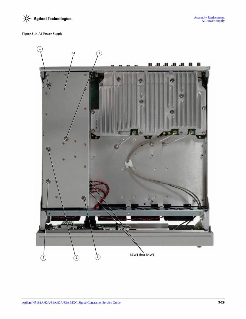
Assembly Replacement A1 Power Supply
Figure 3-14 A1 Power Supply
A1 11
1 1 1B1W1 thru B4W1
Agilent N5161A/62A/81A/82A/83A MXG Signal Generators Service Guide 3-29

Assembly ReplacementA2 Vector Module (N5162A with Option 012 and N5182A Option 1EM with Option 012)
A2 Vector Module (N5162A with Option 012 and N5182A Option 1EM with Option 012)
Tools Required • T-10 driver
• 5/16” open-ended wrench
• needle-nose pliers
Removal Procedure
Refer to Figure 3-16 for this procedure.
1. Go to ”Assembly Installation and Removal Overview” on page 4-2, and complete the ”Assembly Removal and Installation Procedure” on page 4-3.
2. Disconnect the power cord.
3. Remove the covers from the signal generator. Refer to ”Outer Cover” on page 3-4, ”Inner Top Cover” on page 3-6, and ”Inner Bottom Cover” on page 3-8.
4. Remove the rear panel from the signal generator. Refer to ”Rear Panel (N5162A/82A)” on page 3-24.
NOTE The rear panel must be removed to allow the pin connector on the A2 Vector Module to be disconnected from the A3 RF assembly without damaging the connector pins.
5. Place the signal generator flat with the A2 Vector Module facing up and the rear panel facing you.
6. Using the 5/16” open-ended wrench, disconnect W5, W16, W17, and W7.
7. Use the needle-nose pliers to disconnect the following cables,
• W19 (I Input) from A3J15
• W20 (Q Input) from A3J16.
8. Using the T-10 driver, remove the five screws (1) that connect the A2 Vector Module to the chassis.
9. Place your thumbs under the BNC connectors and push up on the A2 Vector Module to release it from the pin connector.
10. Remove the A2 Vector Module.
Replacement Procedure 1. Reverse the order of the removal procedure.
2. Torque all T-10 screws to 9 in–lbs.
3. Torque all BNC connectors to 8 in–lbs.
4. Perform the post-repair performance tests that pertain to this replacement procedure, see Chapter 4, Post-Repair Procedures and Performance Verification.
Agilent N5161A/62A/81A/82A/83A MXG Signal Generators Service Guide 3-30
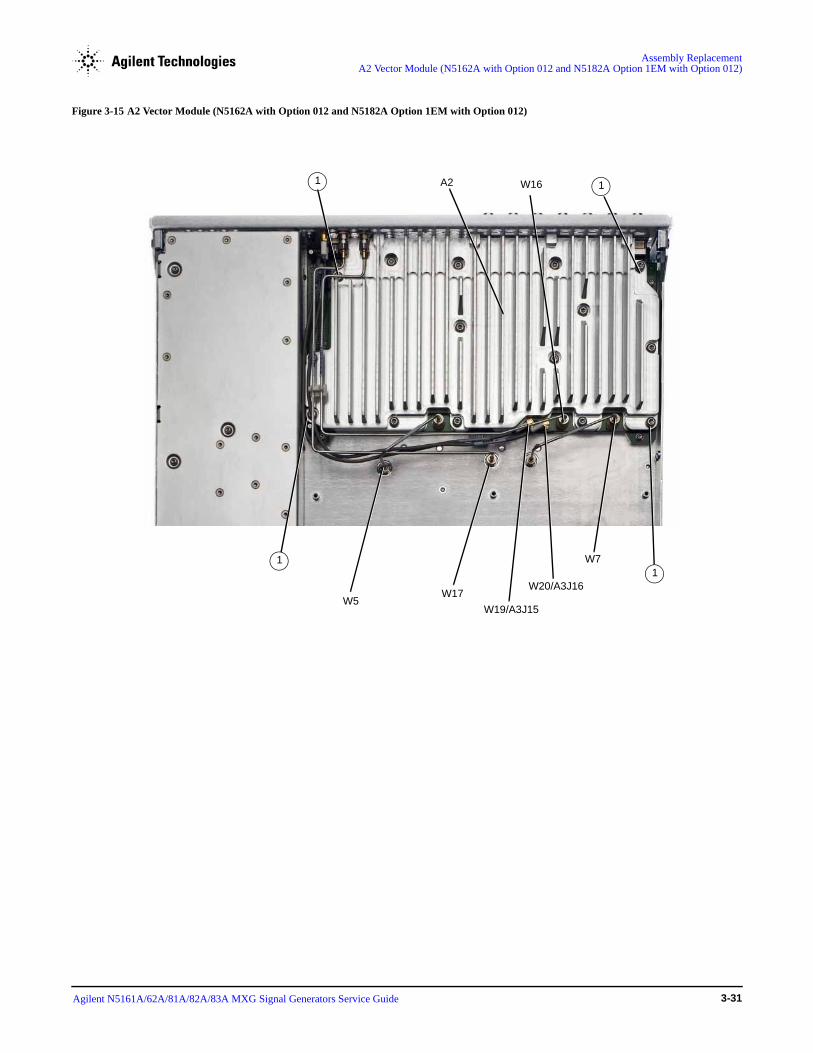
Assembly Replacement A2 Vector Module (N5162A with Option 012 and N5182A Option 1EM with Option 012)
Figure 3-15 A2 Vector Module (N5162A with Option 012 and N5182A Option 1EM with Option 012)
A21 1
11
W5W17
W19/A3J15
W7
W20/A3J16
W16
Agilent N5161A/62A/81A/82A/83A MXG Signal Generators Service Guide 3-31

Assembly ReplacementA2 Vector Module (N5162A/82A without Option 012)
A2 Vector Module (N5162A/82A without Option 012)
Tools Required • T-10 driver
• 5/16” open-ended wrench
• needle-nose pliers
Removal Procedure
Refer to Figure 3-16 for this procedure.
1. Go to ”Assembly Installation and Removal Overview” on page 4-2, and complete the ”Assembly Removal and Installation Procedure” on page 4-3.
2. Disconnect the power cord.
3. Remove the covers from the signal generator. Refer to ”Outer Cover” on page 3-4, ”Inner Top Cover” on page 3-6, and ”Inner Bottom Cover” on page 3-8.
4. Remove the rear panel from the signal generator. Refer to ”Rear Panel (N5162A/82A)” on page 3-24.
NOTE The rear panel must be removed to allow the pin connector on the A2 Vector Module to be disconnected from the A3 RF assembly without damaging the connector pins.
5. Place the signal generator flat with the A2 Vector Module facing up and the rear panel facing you.
6. Using the 5/16” open-ended wrench, disconnect W5, W6, and W7.
7. Use the needle-nose pliers to disconnect the following cables according to the signal generator you have.
• N5162A: W19 (I Input) from A3J15 and W20 (Q Input) from A3J16. (shown in Figure 3-15)
• N5182A: W3 (I Input) from A3J15 and W4 (Q Input) from A3J16.
8. Using the T-10 driver, remove the five screws (1) that connect the A2 Vector Module to the chassis.
9. Place your thumbs under the BNC connectors and push up on the A2 Vector Module to release it from the pin connector.
10. Remove the A2 Vector Module.
Replacement Procedure 1. Reverse the order of the removal procedure.
2. Torque all T-10 screws to 9 in–lbs.
3. Torque all BNC connectors to 8 in–lbs.
4. Perform the post-repair performance tests that pertain to this replacement procedure, see Chapter 4, Post-Repair Procedures and Performance Verification.
Agilent N5161A/62A/81A/82A/83A MXG Signal Generators Service Guide 3-32
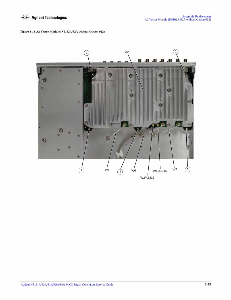
Assembly Replacement A2 Vector Module (N5162A/82A without Option 012)
Figure 3-16 A2 Vector Module (N5162A/82A without Option 012)
A21 1
1 11W5 W6
W3/A3J15
W7W4/A3J16
Agilent N5161A/62A/81A/82A/83A MXG Signal Generators Service Guide 3-33
Assembly ReplacementA3 RF Assembly (N5162A, with and without Option 012, N5182A with Option 012, and N5182A Option 1EM, with and without Option 012)
A3 RF Assembly (N5162A, with and without Option 012, N5182A with Option 012, and N5182A Option 1EM, with and without Option 012)
WARNING Do not disconnect the RF connector cable from the A3 RF assembly or the RF connector itself. Removing the cable will result in instrument failure.
Tools Required • T-10 driver
• 5/16” open-ended wrench
• common screwdriver
Removal Procedure
Refer to Figure 3-17, Figure 3-18 and Figure 3-19 for this procedure.
NOTE Pry slots have been provided on both sides of the A3 RF assembly to aid in removing the board.
1. Go to ”Assembly Installation and Removal Overview” on page 4-2, and complete the ”Assembly Removal and Installation Procedure” on page 4-3.
2. Disconnect the power cord.
3. Remove the covers from the signal generator. Refer to ”Outer Cover” on page 3-4, ”Inner Top Cover” on page 3-6, and ”Inner Bottom Cover” on page 3-8.
4. Place the signal generator flat with the A2 Vector Module facing up and the rear panel facing you.
5. Using the 5/16” open-ended wrench, disconnect the following cables according to the instrument you have.
Instruments without Option 012: W5, W6, and W7.
Instruments with Option 012: W5, W17, and W7.
6. Place the signal generator flat with the A3 RF assembly facing up.
7. Remove the following assemblies, in the order listed
a. ”A4 Internal Memory Card (N5162A/82A only)” (see page 3-52)
b. ”A5 CPU” (see page 3-54)
c. ”Rear Panel (N5162A/82A)” on page 3-24
d. ”Front-Panel” (see page 3-10)
8. Using the T-10 driver, remove the 10 screws (1) that connect the A3 RF assembly to the chassis.
9. Place the tip of a medium common screwdriver into one of the three pry slots on the A3 RF assembly and twist the screwdriver to release the board from the connector pins, see Figure 3-24.
10. Repeat step 9 with the other two pry slots.
11. Remove the A3 RF assembly.
Replacement Procedure 1. Reverse the order of the removal procedure.
2. Torque all screws to 21 in–lbs.
3. Torque all BNC connectors to 8 in–lbs.
4. Perform the post-repair service procedure and performance tests that pertain to this replacement procedure, see Chapter 4, Post-Repair Procedures and Performance Verification.
Agilent N5161A/62A/81A/82A/83A MXG Signal Generators Service Guide 3-34

Assembly Replacement A3 RF Assembly (N5162A, with and without Option 012, N5182A with Option 012, and N5182A Option 1EM,
with and without Option 012)
Figure 3-17 A3 RF Assembly - N5162A and N5182A Option 1EM
W5 W17W7
W5 W6 W7
Instruments without Option 012
Instruments without Option 012
Agilent N5161A/62A/81A/82A/83A MXG Signal Generators Service Guide 3-35

Assembly ReplacementA3 RF Assembly (N5162A, with and without Option 012, N5182A with Option 012, and N5182A Option 1EM, with and without Option 012)
Figure 3-18 A3 RF Assembly - N5162A and N5182A Option 1EM (2 of 3)
111
under ribboncable
11
1
1 11
1
A32
Agilent N5161A/62A/81A/82A/83A MXG Signal Generators Service Guide 3-36
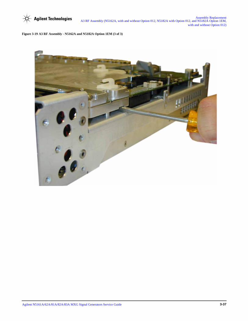
Assembly Replacement A3 RF Assembly (N5162A, with and without Option 012, N5182A with Option 012, and N5182A Option 1EM,
with and without Option 012)
Figure 3-19 A3 RF Assembly - N5162A and N5182A Option 1EM (3 of 3)
Agilent N5161A/62A/81A/82A/83A MXG Signal Generators Service Guide 3-37

Assembly ReplacementA3 RF Assembly - Standard (N5181A/82A)
A3 RF Assembly - Standard (N5181A/82A)
WARNING Do not disconnect the RF connector cable from the A3 RF assembly or the RF connector itself. Removing the cable will result in instrument failure.
Tools Required • T-10 driver
• 5/16” open-ended wrench
• common screwdriver
Removal Procedure
Refer to Figure 3-20, Figure 3-21 and Figure 3-22 for this procedure.
NOTE The RF Connector bracket will need to be disconnected from the chassis before the A3 RF assembly can be removed.
NOTE Pry slots have been provided on both sides of the A3 RF assembly to aid in removing the board.
1. Go to ”Assembly Installation and Removal Overview” on page 4-2, and complete the ”Assembly Removal and Installation Procedure” on page 4-3.
2. Disconnect the power cord.
3. Remove the covers from the signal generator. Refer to ”Outer Cover” on page 3-4, ”Inner Top Cover” on page 3-6, and ”Inner Bottom Cover” on page 3-8.
4. Place the signal generator flat with the A2 Vector Module facing up and the rear panel facing you (N5182A only).
5. Using the 5/16” open-ended wrench, remove the following cables W5, W6, and W7.
6. Place the signal generator flat with the A3 RF assembly facing up.
7. Remove the following assemblies, in the order listed
a. ”A4 Internal Memory Card (N5162A/82A only)” (see page 3-52)
b. ”A5 CPU” (see page 3-54)
c. ”Rear Panel (N5161A/81A)” (see page 3-22), or ”Rear Panel (N5162A/82A)” (see page 3-24)
d. ”Front-Panel” (see page 3-10)
8. Using the T-10 driver, remove the 10 screws (1) that connect the A3 RF assembly to the chassis.
9. Using the T-10 driver to remove the three screws (2) that connect the RF connector bracket to the chassis.
CAUTION The RF Connector can be easily damaged. Use extreme caution when disconnecting the RF connector bracket from the instrument chassis.
10. Place the tip of a medium common screwdriver into one of the three pry slots on the A3 RF assembly and twist the screwdriver to release the board from the connector pins, see Figure 3-22.
11. Repeat step 10 with the other two pry slots.
12. Remove the A3 RF assembly.
Replacement Procedure 1. Reverse the order of the removal procedure.
2. Torque all screws to 21 in–lbs.
3. Torque all BNC connectors to 8 in–lbs.
4. Perform the post-repair service procedure and performance tests that pertain to this replacement procedure, see Chapter 4, Post-Repair Procedures and Performance Verification.
Agilent N5161A/62A/81A/82A/83A MXG Signal Generators Service Guide 3-38

Assembly Replacement A3 RF Assembly - Standard (N5181A/82A)
Figure 3-20 A3 RF Assembly - Standard (N5181A/82A) (1 of 3)
W5W6
W7
(N5182A only)
(N5182A only)(N5182A only)
Agilent N5161A/62A/81A/82A/83A MXG Signal Generators Service Guide 3-39

Assembly ReplacementA3 RF Assembly - Standard (N5181A/82A)
Figure 3-21 A3 RF Assembly - Standard (N5181A/82A) (2 of 3)
1 11
under ribboncable
1 1
1
1 11 1A3
2
Agilent N5161A/62A/81A/82A/83A MXG Signal Generators Service Guide 3-40

Assembly Replacement A3 RF Assembly - Standard (N5181A/82A)
Figure 3-22 A3 RF Assembly - Standard (N5181A/82A) (3 of 3)
Agilent N5161A/62A/81A/82A/83A MXG Signal Generators Service Guide 3-41

Assembly ReplacementA3 RF Assembly - N5161A and N5181A Option 1EM
A3 RF Assembly - N5161A and N5181A Option 1EM
WARNING Do not disconnect the RF connector cable from the A3 RF assembly or the RF connector itself. Removing the cable will result in instrument failure.
Tools Required • T-10 driver
• 5/16” open-ended wrench
• common screwdriver
Removal Procedure
Refer to Figure 3-23 and Figure 3-24 for this procedure.
NOTE Pry slots have been provided on both sides of the A3 RF assembly to aid in removing the board.
1. Go to ”Assembly Installation and Removal Overview” on page 4-2, and complete the ”Assembly Removal and Installation Procedure” on page 4-3.
2. Disconnect the power cord.
3. Remove the covers from the signal generator. Refer to ”Outer Cover” on page 3-4, ”Inner Top Cover” on page 3-6, and ”Inner Bottom Cover” on page 3-8.
4. Place the signal generator flat with the A3 RF assembly facing up.
5. Remove the following assemblies, in the order listed
a. ”A5 CPU” (see page 3-54)
b. ”Rear Panel (N5161A/81A)” (see page 3-22)
c. ”Front-Panel” (see page 3-10)
6. Using the T-10 driver, remove the 10 screws (1) that connect the A3 RF assembly to the chassis.
7. Place the tip of a medium common screwdriver into one of the three pry slots on the A3 RF assembly and twist the screwdriver to release the board from the connector pins, see Figure 3-24.
8. Repeat step 7 with the other two pry slots.
9. Remove the A3 RF assembly.
Replacement Procedure 1. Reverse the order of the removal procedure.
2. Torque all screws to 21 in–lbs.
3. Torque all BNC connectors to 8 in–lbs.
4. Perform the post-repair service procedure and performance tests that pertain to this replacement procedure, see Chapter 4, Post-Repair Procedures and Performance Verification.
Agilent N5161A/62A/81A/82A/83A MXG Signal Generators Service Guide 3-42

Assembly Replacement A3 RF Assembly - N5161A and N5181A Option 1EM
Figure 3-23 A3 RF Assembly - 1EM (1 of 2)
1
11
1
1
A3
1 11
under ribboncable
11
Agilent N5161A/62A/81A/82A/83A MXG Signal Generators Service Guide 3-43

Assembly ReplacementA3 RF Assembly - N5161A and N5181A Option 1EM
Figure 3-24 A3 RF Assembly - 1EM (2 of 2)
Agilent N5161A/62A/81A/82A/83A MXG Signal Generators Service Guide 3-44

Assembly Replacement A3 RF Assembly - N5161A and N5181A Option 1EM
This page intentionally left blank.
Agilent N5161A/62A/81A/82A/83A MXG Signal Generators Service Guide 3-45
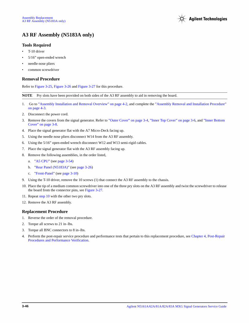
Assembly ReplacementA3 RF Assembly (N5183A only)
A3 RF Assembly (N5183A only)
Tools Required • T-10 driver
• 5/16” open-ended wrench
• needle-nose pliers
• common screwdriver
Removal Procedure
Refer to Figure 3-25, Figure 3-26 and Figure 3-27 for this procedure.
NOTE Pry slots have been provided on both sides of the A3 RF assembly to aid in removing the board.
1. Go to ”Assembly Installation and Removal Overview” on page 4-2, and complete the ”Assembly Removal and Installation Procedure” on page 4-3.
2. Disconnect the power cord.
3. Remove the covers from the signal generator. Refer to ”Outer Cover” on page 3-4, ”Inner Top Cover” on page 3-6, and ”Inner Bottom Cover” on page 3-8.
4. Place the signal generator flat with the A7 Micro-Deck facing up.
5. Using the needle nose pliers disconnect W14 from the A3 RF assembly.
6. Using the 5/16” open-ended wrench disconnect W12 and W13 semi-rigid cables.
7. Place the signal generator flat with the A3 RF assembly facing up.
8. Remove the following assemblies, in the order listed,
a. ”A5 CPU” (see page 3-54)
b. ”Rear Panel (N5183A)” (see page 3-26)
c. ”Front-Panel” (see page 3-10)
9. Using the T-10 driver, remove the 10 screws (1) that connect the A3 RF assembly to the chassis.
10. Place the tip of a medium common screwdriver into one of the three pry slots on the A3 RF assembly and twist the screwdriver to release the board from the connector pins, see Figure 3-27.
11. Repeat step 10 with the other two pry slots.
12. Remove the A3 RF assembly.
Replacement Procedure 1. Reverse the order of the removal procedure.
2. Torque all screws to 21 in–lbs.
3. Torque all BNC connectors to 8 in–lbs.
4. Perform the post-repair service procedure and performance tests that pertain to this replacement procedure, see Chapter 4, Post-Repair Procedures and Performance Verification.
Agilent N5161A/62A/81A/82A/83A MXG Signal Generators Service Guide 3-46
Assembly Replacement A3 RF Assembly (N5183A only)
Figure 3-25A3 RF Assembly (N5183A only) (1 of 3)
W14
W13 W12
Agilent N5161A/62A/81A/82A/83A MXG Signal Generators Service Guide 3-47

Assembly ReplacementA3 RF Assembly (N5183A only)
Figure 3-26 A3 RF Assembly (N5183A only) (2 of 3)
1 111 1
1
1 11 1A3
under ribboncable
Agilent N5161A/62A/81A/82A/83A MXG Signal Generators Service Guide 3-48

Assembly Replacement A3 RF Assembly (N5183A only)
Figure 3-27 A3 RF Assembly - (N5183A only) (3 of 3)
Agilent N5161A/62A/81A/82A/83A MXG Signal Generators Service Guide 3-49
Assembly ReplacementA3BT1 Battery
A3BT1 Battery
WARNING This battery contains lithium. Do not incinerate or puncture this battery. Do not install this battery backwards. To dispose of the battery in a safe manner. Refer to ”Lithium Battery Disposal” on page 5-2.
NOTE The battery is part of the power off circuitry. Removing the battery will not cause any stored data to be lost.
Tools Required • T-10 driver
• small common screw driver
Removal Procedure
Refer to Figure 3-28 for this procedure.
1. Disconnect the power cord.
2. Remove the covers from the signal generator. Refer to ”Outer Cover” on page 3-4 and ”Inner Bottom Cover” on page 3-8.
3. Place the signal generator flat with the A3 RF assembly facing up and the front-panel towards you.
4. Using the flat-head screw driver, remove the A3BT1 by leveraging the battery out of its socket.
Replacement Procedure 1. Reverse the remaining steps of the removal procedure.
NOTE To install the battery, the positive side is aligned with the positive sign on the A3 RF assembly’s battery clip.
2. Perform the post-repair performance tests that pertain to this replacement procedure, see Chapter 4, Post-Repair Procedures and Performance Verification.
Agilent N5161A/62A/81A/82A/83A MXG Signal Generators Service Guide 3-50

Assembly Replacement A3BT1 Battery
Figure 3-28 A3BT1 Battery
A3BT1
Agilent N5161A/62A/81A/82A/83A MXG Signal Generators Service Guide 3-51

Assembly ReplacementA4 Internal Memory Card (N5162A/82A only)
A4 Internal Memory Card (N5162A/82A only)
Tools Required • T-10 driver
Removal Procedure
Refer to Figure 3-29 for this procedure.
1. Disconnect the power cord.
2. Remove the covers from the signal generator. Refer to ”Outer Cover” on page 3-4 and ”Inner Bottom Cover” on page 3-8.
3. Place the signal generator flat and upside down with the rear panel facing you.
4. Using the T-10 driver, remove the screw (1) that attaches the A4 Internal Memory Card to the A3 RF assembly.
5. Remove the A4 Internal Memory Card by gently rocking it side to side to release the pin.
Replacement Procedure 1. Reverse the order of the removal procedure.
CAUTION The A4 Internal Memory Card pin can be re-installed incorrectly. To insure proper installation carefully align the connector on the A4 Internal Memory Card with the connector on the A3 RF assembly.
2. Torque all screws to 9 in–lbs.
3. Perform the post-repair performance tests that pertain to this replacement procedure, see Chapter 4, Post-Repair Procedures and Performance Verification.
Agilent N5161A/62A/81A/82A/83A MXG Signal Generators Service Guide 3-52

Assembly Replacement A4 Internal Memory Card (N5162A/82A only)
Figure 3-29 A4 Internal Memory Card
A41
Agilent N5161A/62A/81A/82A/83A MXG Signal Generators Service Guide 3-53

Assembly ReplacementA5 CPU
A5 CPU
Tools Required • T-8 driver
Removal Procedure
Refer to Figure 3-30 for this procedure.
CAUTION There are three pin connectors attaching the A5 CPU to the A3 RF assembly. They are located on the short end of the A5 CPU board, closest to the front-panel. Use caution when removing the A5 CPU board.
1. Go to ”Assembly Installation and Removal Overview” on page 4-2, and complete the ”Assembly Removal and Installation Procedure” on page 4-3.
2. Disconnect the power cord.
3. Remove the covers from the signal generator. Refer to ”Outer Cover” on page 3-4 and ”Inner Bottom Cover” on page 3-8.
4. Place the signal generator flat and upside down with the front-panel facing you.
5. Using the T-8 driver, remove the four screws (1) that attach the A5 CPU to the A3 RF assembly.
6. Remove the A5 CPU.
7. Disconnect W9.
Replacement Procedure 1. Reverse the order of the removal procedure.
2. Torque all screws to 9 in–lbs.
3. Perform the post-repair service procedure and performance tests that pertain to this replacement procedure, see Chapter 4, Post-Repair Procedures and Performance Verification.
Agilent N5161A/62A/81A/82A/83A MXG Signal Generators Service Guide 3-54

Assembly Replacement A5 CPU
Figure 3-30 A5 CPU
W9
1
1
11
A5
Agilent N5161A/62A/81A/82A/83A MXG Signal Generators Service Guide 3-55
Assembly ReplacementA7 Micro-Deck (N5183A only - Standard)
A7 Micro-Deck (N5183A only - Standard)
Tools Required • T-10 driver
• 5/16” open-ended wrench
Removal Procedure
Refer to Figure 3-31 for this procedure.
1. Go to ”Assembly Installation and Removal Overview” on page 4-2, and complete the ”Assembly Removal and Installation Procedure” on page 4-3.
2. Disconnect the power cord.
3. Remove the covers from the signal generator. Refer to ”Outer Cover” on page 3-4, ”Inner Top Cover” on page 3-6, and ”Inner Bottom Cover” on page 3-8.
4. Remove the rear panel from the signal generator. Refer to ”Rear Panel (N5183A)” on page 3-26.
NOTE The rear panel must be removed to allow the pin connector on the A7 Micro Deck to be disconnected from the A3 RF assembly without damaging the connector pins.
5. Using a 5/16” open-ended wrench, disconnect one end of the following cables, see Figure 3-31 to determine which end to disconnect.
W12 semi-rigid cable from the A3 RF assembly.
W13 semi-rigid cable from the A3 RF assembly.
6. Using a 5/16” open-ended wrench, disconnect the following semi-rigid cable according to the signal generator you have.
520 with a 3.5mm RF connector: W10 from the mechanical attenuator (1).
520 with a Type-N RF connector: W11 from the mechanical attenuator (1).
532/540: W9 from the mechanical attenuator (1).
7. Disconnect W14 from A7J15.
8. Disconnect W15 from A7J14.
9. Using the T-10 driver, remove the eight screws (2) that secure the A7 Micro Deck to the chassis.
10. Remove the A7 Micro Deck.
Replacement Procedure
Refer to Figure 3-32 for this procedure.
1. Using the T-10 driver, remove the five screws (3) that secure the replacement A7 Micro Deck to the shipping chassis.
2. Carefully slide the replacement A7 Micro Deck out of the shipping chassis.
3. Reverse the order of the removal procedure.
4. Torque all screws to 9 in–lbs.
5. Perform the post-repair performance tests that pertain to this replacement procedure, see Chapter 4, Post-Repair Procedures and Performance Verification.
6. Slide the old A7 Micro Deck into the shipping chassis.
7. Secure it to the shipping chassis by installing the five screws removed in step 1.
NOTE If you lose any screws there are five extra screws located on one end of the shipping chassis.
8. Torque all screws to 9 in–lbs.
9. Return the A7 Micro Deck to Agilent Technologies. See ”Shipping a Defective Assembly Back to Agilent Technologies” on page 2-1.
Agilent N5161A/62A/81A/82A/83A MXG Signal Generators Service Guide 3-56
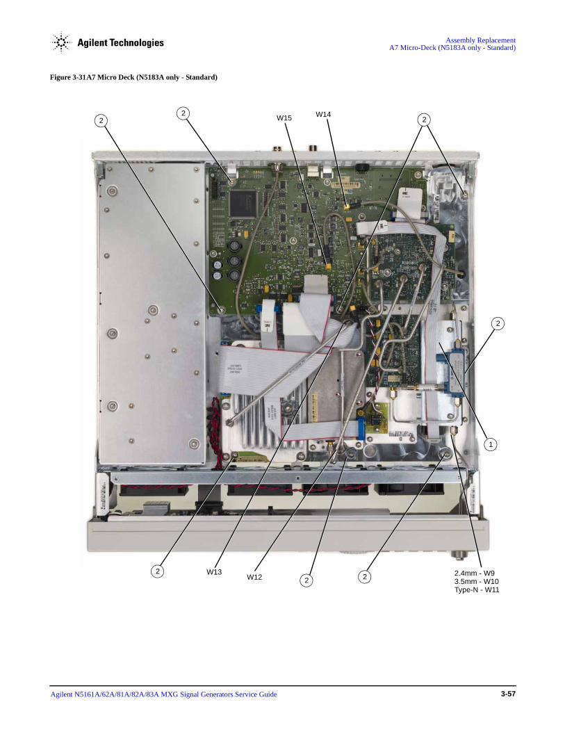
Assembly Replacement A7 Micro-Deck (N5183A only - Standard)
Figure 3-31A7 Micro Deck (N5183A only - Standard)
W15 W14
2.4mm - W93.5mm - W10Type-N - W11
W13W12
1
22 2
2
2
2 2
Agilent N5161A/62A/81A/82A/83A MXG Signal Generators Service Guide 3-57

Assembly ReplacementA7 Micro-Deck (N5183A only - Standard)
Figure 3-32A7 Micro Deck Replacement
33
33
3
Extra screws
Agilent N5161A/62A/81A/82A/83A MXG Signal Generators Service Guide 3-58

Assembly Replacement A7 Micro-Deck (N5183A only - Option 1EM)
A7 Micro-Deck (N5183A only - Option 1EM)
Tools Required • T-10 driver
• 5/16” open-ended wrench
Removal Procedure
Refer to Figure 3-33 for this procedure.
1. Go to ”Assembly Installation and Removal Overview” on page 4-2, and complete the ”Assembly Removal and Installation Procedure” on page 4-3.
2. Disconnect the power cord.
3. Remove the covers from the signal generator. Refer to ”Outer Cover” on page 3-4, ”Inner Top Cover” on page 3-6, and ”Inner Bottom Cover” on page 3-8.
4. Remove the rear panel from the signal generator. Refer to ”Rear Panel (N5183A)” on page 3-26.
NOTE The rear panel must be removed to allow the pin connector on the A7 Micro Deck to be disconnected from the A3 RF assembly without damaging the connector pins.
5. Using a 5/16” open-ended wrench, disconnect one end of the following cables, see Figure 3-33 to determine which end to disconnect.
W12 semi-rigid cable from the A3 RF assembly.
W13 semi-rigid cable from the A3 RF assembly.
6. Disconnect W14 from A7J15.
7. Disconnect W15 from A7J14.
8. Using the T-10 driver, remove the eight screws (1) that secure the A7 Micro Deck to the chassis.
9. Remove the A7 Micro Deck.
Replacement Procedure
Refer to Figure 3-34 for this procedure.
1. Using the T-10 driver, remove the five screws (3) that secure the replacement A7 Micro Deck to its packaging.
2. Carefully slide the replacement A7 Micro Deck out of its packaging.
3. Reverse the order of the removal procedure.
4. Torque all screws to 9 in–lbs.
5. Perform the post-repair performance tests that pertain to this replacement procedure, see Chapter 4, Post-Repair Procedures and Performance Verification.
Agilent N5161A/62A/81A/82A/83A MXG Signal Generators Service Guide 3-59
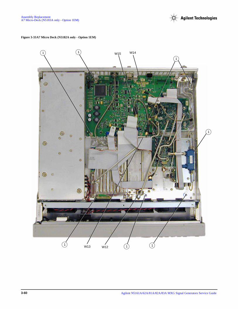
Assembly ReplacementA7 Micro-Deck (N5183A only - Option 1EM)
Figure 3-33A7 Micro Deck (N5182A only - Option 1EM)
W15 W14
W13 W12
1
1
1
1 1
1
1
Agilent N5161A/62A/81A/82A/83A MXG Signal Generators Service Guide 3-60

Assembly Replacement A7 Micro-Deck (N5183A only - Option 1EM)
Figure 3-34A7 Micro Deck Replacement
33
33
3
Extra screws
Agilent N5161A/62A/81A/82A/83A MXG Signal Generators Service Guide 3-61

Assembly ReplacementA8 Floating BNC Bypass (N5183A only)
A8 Floating BNC Bypass (N5183A only)
Tools Required • 5/8” hex-nut driver
• needle-nose pliers
Removal Procedure
Refer to Figure 3-35 for this procedure.
1. Disconnect the power cord.
2. Remove the inner cover and outer top cover from the signal generator. Refer to ”Outer Cover” on page 3-4, ”Inner Top Cover” on page 3-6.
3. Disconnect W15 from A7J14.
4. Using the 5/8” hex-nut driver, remove the nut and washer securing the A8 Floating BNC Bypass to the rear panel.
5. Remove the A8 Floating BNC Bypass.
Replacement Procedure 1. Reverse the order of the removal procedure.
2. Torque all screws to 9 in–lbs.
3. Perform the post-repair performance tests that pertain to this replacement procedure, see Chapter 4, Post-Repair Procedures and Performance Verification.
Agilent N5161A/62A/81A/82A/83A MXG Signal Generators Service Guide 3-62
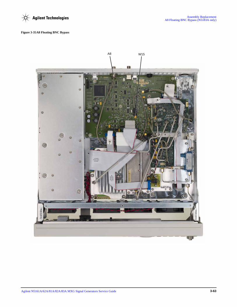
Assembly Replacement A8 Floating BNC Bypass (N5183A only)
Figure 3-35A8 Floating BNC Bypass
W15A8
Agilent N5161A/62A/81A/82A/83A MXG Signal Generators Service Guide 3-63

Assembly ReplacementRF Connector (N5183A only - Standard)
RF Connector (N5183A only - Standard)
Tools Required • 5/16” open-ended wrench
Removal Procedure
Refer to Figure 3-36 for this procedure.
1. Disconnect the power cord.
2. Remove the covers from the signal generator. Refer to ”Outer Cover” on page 3-4, ”Inner Top Cover” on page 3-6, and ”Inner Bottom Cover” on page 3-8.
3. Remove the front-panel from the signal generator. Refer to ”Front-Panel” on page 3-10.
4. Using a 5/16” open-ended wrench, disconnect the following semi-rigid cable according to the signal generator you have.
520 with a 3.5mm RF connector: W10 from the RF connector (1).
520 with a Type-N RF connector: W11 from the RF connector (1).
532/540: W9 from the RF Connector (1).
5. Remove the RF Connector.
Replacement Procedure 1. Reverse the order of the removal procedure.
2. Torque screw to 9 in–lbs.
3. Torque the new RF connector to 75 in–lbs.
4. Perform the post-repair performance tests that pertain to this replacement procedure, see Chapter 4, Post-Repair Procedures and Performance Verification.
Agilent N5161A/62A/81A/82A/83A MXG Signal Generators Service Guide 3-64
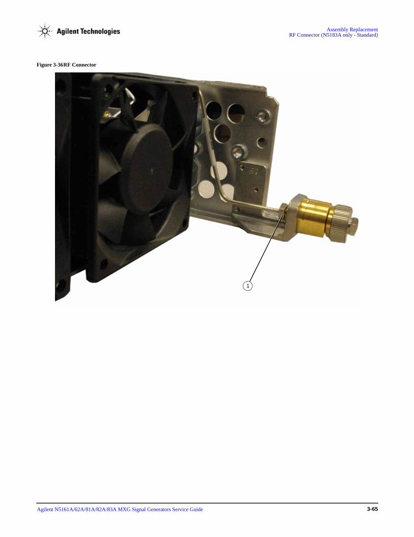
Assembly Replacement RF Connector (N5183A only - Standard)
Figure 3-36RF Connector
1
Agilent N5161A/62A/81A/82A/83A MXG Signal Generators Service Guide 3-65

Assembly ReplacementB1 thru B4 Fans
B1 thru B4 Fans
Tools Required • T-10 driver
• T-20 driver
• needle-nose pliers
Removal Procedure
Refer to Figure 3-37 and Figure 3-38 for this procedure.
1. Disconnect the power cord.
2. Remove the covers from the signal generator. Refer to ”Outer Cover” on page 3-4, ”Inner Top Cover” on page 3-6, and ”Inner Bottom Cover” on page 3-8.
NOTE If you are replacing the B1 Fan, remove the A1 Power Supply. Refer to ”A1 Power Supply” on page 3-28.
3. Place the signal generator flat with the A2 Vector Module facing up and the front-panel facing you.
4. Using the T-10 driver, press the connector latch to disconnect the fan cable (1) from the A2 Power Supply.
5. Use the T-20 driver to push the rivet (2) out until you can remove it with your fingers.
6. Remove the fan, releasing the fan cable from the cable clips.
Replacement Procedure 1. Reverse the order of the removal procedure.
NOTE To re-install the rivets, use the needle-nose pliers to depress the rivet tip before inserting it into the chassis hole.
2. Perform the post-repair performance tests that pertain to this replacement procedure, see Chapter 4, Post-Repair Procedures and Performance Verification.
Agilent N5161A/62A/81A/82A/83A MXG Signal Generators Service Guide 3-66
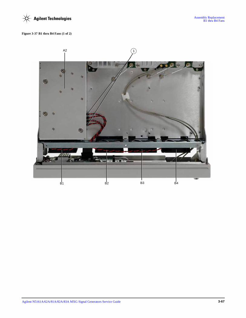
Assembly Replacement B1 thru B4 Fans
Figure 3-37 B1 thru B4 Fans (1 of 2)
A2
B1 B2 B3 B4
1
Agilent N5161A/62A/81A/82A/83A MXG Signal Generators Service Guide 3-67
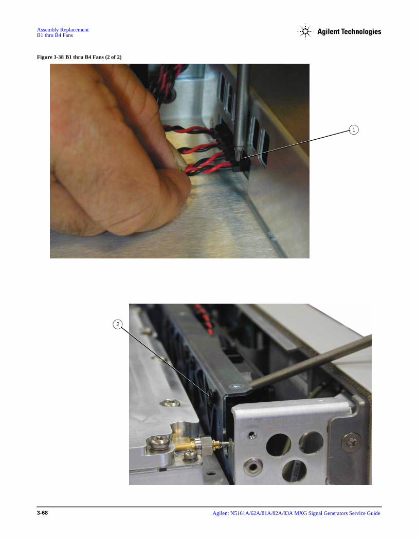
Assembly ReplacementB1 thru B4 Fans
Figure 3-38 B1 thru B4 Fans (2 of 2)
1
2
Agilent N5161A/62A/81A/82A/83A MXG Signal Generators Service Guide 3-68

4 Post-Repair Procedures and Performance Verification
Post Repair Procedures
CAUTION After changing an assembly, but before performance verification, Agilent recommends that the most recent firmware is loaded into the instrument.
To avoid internal calibration failures and potential post-repair errors, before removing any instrument assembly, the instrument’s static and dynamic arrays must be configured for the exchange of assemblies. The process to do the appropriate configuration is performed automatically by the MXG with the Assembly Installation and Removal Overview front panel softkeys. Refer to the Assembly Installation and Removal Overview and to the “Hardware Assembly Installation and Removal Softkeys” on page 4-2.
For the instrument to meet performance specifications and for accurate self-test results, allow a warm up period of 45 minutes within an operational temperature range of 0 to 55 °C. For more information, refer to the MXG signal generator Data Sheet.
The ability to ensure proper hardware compatibility when an assembly is replaced in the MXG, is based on the capability of the product to save and reconfigure its arrays. To ensure that existing and new hardware is appropriately configured correctly, the static and dynamic arrays associated with the different assemblies must be modified as needed.
The process to do the appropriate configuration is performed automatically by the MXG with the Assembly Installation and Removal Overview front panel softkeys.
The corresponding assembly removal softkey is pressed once prior to a specific assembly being permanently removed for replacement from the instrument. Once the removed assembly has been permanently replaced the corresponding installation softkey is pressed, completing the hardware and installation.
Agilent Technologies N5161A/62A/81A/82A/83A MXG Signal Generators Service Guide 4- 1

Post-Repair Procedures and Performance VerificationPost Repair Procedures
Assembly Installation and Removal Overview
Figure 4-1 Hardware Assembly Installation and Removal Softkeys
Utility > More 2 of 2 > ServiceFor details on each key, use key help. Refer to the User’s Guide.
Note:
Each Remove Assembly softkey (CPU/RF/BBG/MW) when enabled will display a message in the lower left quadrant of display indicating assembly prepared for removal or removal has been aborted.
Each Install Assembly softkey, when enabled will display a message in the lower left quadrant of display indicating assembly prepared for installation or installation has been aborted.
N5162A/82A only
N5183A only
Whether a softkey is available
depends on the model of MXG.
Note: When pressed, a Confirm Removal menu (similar to the one shown here for the CPU assembly) is opened for the RF, BBG, and MW assemblies too.
Whether a softkey is available
depends on the model of MXG.
N5162A/82A only
N5183A only
Note: When pressed, a Confirm Install menu (similar to the one shown here for the CPU assembly) is opened for the RF, BBG, and MW assemblies too.
Agilent Technologies N5161A/62A/81A/82A/83A MXG Signal Generators Service Guide 4-2

Post-Repair Procedures and Performance Verification Post Repair Procedures
Assembly Removal and Installation Procedure
NOTE This section is meant to be a high level overview of the process for replacing an assembly.
1. Faulty/bad board assembly is identified by using the troubleshooting information in Chapter 1.
2. Before removing the bad assembly, use the Remove Assembly service menu to transfer the assembly’s array information, by pressing the corresponding softkey: Prepare <CPU/RF/BBG> Assembly For Removal. (Refer to Assembly Installation and Removal Overview.)
CAUTION Do not proceed with assembly replacement until step 2 has been completed. Failure to perform this step can result in the hardware not functioning optimally, resulting in instrument errors and possibly self-test failures.
3. Replace the faulty/bad assembly.
4. Press the corresponding Install Assembly menu softkey: Finalize <CPU/RF/BBG> Assembly Installation. (Refer to Assembly Installation and Removal Overview.)
CAUTION Do not proceed with Assembly replacement until step 4 has been completed. Failure to perform this step can result in the hardware not functioning optimally, resulting in instrument errors and possibly self-test failures.
Service Procedure
CAUTION After replacing an assembly, it is critical to do a backup or restore in the instrument—as indicated in the tables below—to return the instrument to full configuration capability. Refer to Table 4-1 and Table 4-2 on page 3.
After replacing an assembly, check the following tables to see if you should run the service procedure. If your instrument has firmware version A.01.04, you must upgrade to A.01.10 or later prior to replacing any assembly. If you do not upgrade to A.01.10 or later your license key data will not be available and all license key enabled options will not work.
• If you did not upgrade your firmware to A.01.10 prior to replacing an assembly refer to Table 4-1.
• If you did upgrade your firmware to A.01.10 or later, refer to Table 4-2.
Table 4-1 Assembly Replaced with A.01.04 firmware installed – Backup
Condition Procedure
Upgrading from A.01.04 to A.01.10 or later.
With Error:
“617 Configuration Error: Instrument licenses have not been copied to backup storage. Use the service procedure to copy license keys to backup storage”
1. Turn the signal generator off.
2. Press and hold Preset, turn the signal generator on, continue to hold Preset for 10 seconds.
3. Press: Continue > Next Page > Backup License Data > Done
4. Cycle the power on the signal generator.
Cannot upgrade to A.01.10 or later due to a hardware failure.
1. Replace the A5 CPU. Refer to Chapter 3, “Assembly Replacement.”
2. Upgrade firmware.
All other conditions not mentioned above Not supported. Upgrade to A.01.10 or later.
Table 4-2 Assembly Replaced with A.01.10 or later firmware installed – Restore/Backup
Condition Procedure
Installed new A5 CPU assembly.
With Error:
“617 Configuration Error: The instrument has no frequency range option installed. Use the service procedure to recover instrument licenses from the backup.”
1. Turn the signal generator off.
2. Press and hold Preset, turn the signal generator on, continue to hold Preset for 10 seconds.
3. Press: Continue > Next Page > Restore License Data from Backup > Done
4. Cycle the power on the signal generator.
NOTE If this procedure fails, the signal generator may be limited to 1 GHz and all options could be missing. Contact an Agilent Technologies service support person for assistance.
Agilent Technologies N5161A/62A/81A/82A/83A MXG Signal Generators Service Guide 4-3

Post-Repair Procedures and Performance VerificationPost Repair Procedures
Post-Repair Overview
N5161A/62A/81A/82A
Replacement assemblies are fully calibrated and do not require any adjustments. The factory completes a performance test on each replacement assembly, so a comprehensive performance test is not required by the customer upon receipt and installation of an assembly. A manual performance test is recommended to check basic operation.
N5183A
Because of the interdependency between assemblies, replacement assemblies are partly calibrated and require limited adjustments to optimize performance. Once adjustments are completed, the N5183A requires full performance testing.
Manual Performance Tests
To ensure the signal generator is meeting all published specifications, Table 4-3 lists the recommended manual performance verification tests to be performed after a specific assembly has been repaired or replaced.
Installed new A3 RF assembly.
With Error:
“617 Configuration Error: Instrument licenses have not been copied to the backup storage. Use the service procedure to copy license keys to backup storage.”
1. Turn the signal generator off.
2. Press and hold Preset, turn the signal generator on, continue to hold Preset for 10 seconds.
3. Press: Continue > Next Page > Backup License Data > Done
4. Cycle the power on the signal generator.
NOTE If this procedure fails, the signal generator may be limited to 1 GHz and all options could be missing. Contact an Agilent Technologies service support person for assistance.
A3 RF assembly backup license keys and instrument serial number do not match.
With Error:
“617 Configuration Error: The backup memory contains license keys for serial number <serial number>. Use the service procedure to overwrite the backup memory.”
1. Turn the signal generator off.
2. Press and hold Preset, turn the signal generator on, continue to hold Preset for 10 seconds.
3. Press: Continue > Next Page > Backup License Data > Done
4. Cycle the power on the signal generator.
NOTE If this procedure fails, the signal generator may be limited to 1 GHz and all options could be missing. Contact an Agilent Technologies service support person for assistance.
Installed an A3 RF assembly that was previously used in another instrument.
With Error:
“617 Configuration Error: The backup memory contains license keys for serial number <serial number>. Use the service procedure to overwrite the backup memory.
• If this is a temporary change, ignore the message.
• If this is a permanent change run the service procedure.
1. Turn the signal generator off.
2. Press and hold Preset, turn the signal generator on, continue to hold Preset for 10 seconds.
3. Press: Continue > Next Page > Backup License Data > Done
4. Cycle the power on the signal generator.
NOTE If this procedure fails, the signal generator may be limited to 1 GHz and all options could be missing. Contact an Agilent Technologies service support person for assistance.
Installed an A5 CPU assembly that was previously used in another instrument.
• If this is a temporary change, ignore the message.
• If this is meant to be a permanent change, Agilent does not support it. A new A5 CPU must be installed.
Table 4-2 Assembly Replaced with A.01.10 or later firmware installed – Restore/Backup (Continued)
Condition Procedure
Agilent Technologies N5161A/62A/81A/82A/83A MXG Signal Generators Service Guide 4-4
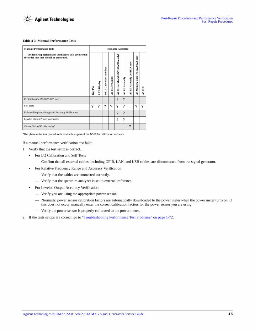
Post-Repair Procedures and Performance Verification Post Repair Procedures
If a manual performance verification test fails:
1. Verify that the test setup is correct.
• For I/Q Calibration and Self Tests
— Confirm that all external cables, including GPIB, LAN, and USB cables, are disconnected from the signal generator.
• For Relative Frequency Range and Accuracy Verification
— Verify that the cables are connected correctly.
— Verify that the spectrum analyzer is set to external reference.
• For Leveled Output Accuracy Verification
— Verify you are using the appropriate power sensor.
— Normally, power sensor calibration factors are automatically downloaded to the power meter when the power meter turns on. If this does not occur, manually enter the correct calibration factors for the power sensor you are using.
— Verify the power sensor is properly calibrated to the power meter.
2. If the tests setups are correct, go to “Troubleshooting Performance Test Problems” on page 1-72.
Table 4-3 Manual Performance Tests
Manuals Performance Tests The following performance verification tests are listed in the order that they should be performed.
Replaced Assembly
Key
Pad
LC
D D
isp
lay
DC
-AC
Inv
erte
r In
terf
ace
A1
Pow
er S
up
ply
A2
Vec
tor
Mod
ule
(N
5162
A/8
2A o
nly
)
A3
RF
Ass
embl
y
A3
RF
Ass
embl
y (N
5183
A o
nly
)
A4
Mem
ory
Ch
ip (
N51
62A
/82A
onl
y)
A5
CP
U
I/Q Calibration (N5162A/82A only) ? ?Self Tests ? ? ? ? ? ? ? ?Relative Frequency Range and Accuracy Verification ? ?Leveled Output Power Verification ? ?
0Phase Noise (N5183A only)a
aThe phase noise test procedure is available as part of the N5183A calibration software.
?
Agilent Technologies N5161A/62A/81A/82A/83A MXG Signal Generators Service Guide 4-5
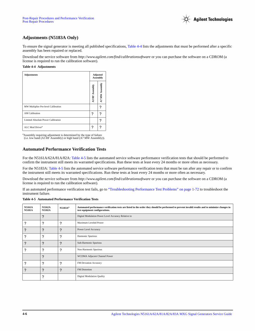
Post-Repair Procedures and Performance VerificationPost Repair Procedures
Adjustments (N5183A Only)
To ensure the signal generator is meeting all published specifications, Table 4-4 lists the adjustments that must be performed after a specific assembly has been repaired or replaced.
Download the service software from http://www.agilent.com/find/calibrationsoftware or you can purchase the software on a CDROM (a license is required to run the calibration software).
Automated Performance Verification Tests
For the N5161A/62A/81A/82A: Table 4-5 lists the automated service software performance verification tests that should be performed to confirm the instrument still meets its warranted specifications. Run these tests at least every 24 months or more often as necessary.
For the N5183A: Table 4-5 lists the automated service software performance verification tests that must be ran after any repair or to confirm the instrument still meets its warranted specifications. Run these tests at least every 24 months or more often as necessary.
Download the service software from http://www.agilent.com/find/calibrationsoftware or you can purchase the software on a CDROM (a license is required to run the calibration software).
If an automated performance verification test fails, go to “Troubleshooting Performance Test Problems” on page 1-72 to troubleshoot the instrument failure.
Table 4-4 Adjustments
Adjustments
Adjusted Assembly
A3
RF
Ass
embl
y
A7
MW
Ass
embl
y
MW Multiplier Pre-level Calibration ?AM Calibration ? ?Limited Absolute Power Calibration ?
ALC Mod Drivera
aAssembly requiring adjustment is determined by the type of failure (i.e. low band (A3 RF Assembly) or high band (A7 MW Assembly)).
? ?
Table 4-5 Automated Performance Verification Tests
N5161A N5181A
N5162A N5182A
N5183Aa Automated performance verification tests are listed in the order they should be performed to prevent invalid results and to minimize changes in test equipment configurations.
? Digital Modulation Power Level Accuracy Relative to
? ? ? Maximum Leveled Power
? ? ? Power Level Accuracy
? ? ? Harmonic Spurious
? ? ? Sub-Harmonic Spurious
? ? ? Non-Harmonic Spurious
? WCDMA Adjacent Channel Power
? ? ? FM Deviation Accuracy
? ? ? FM Distortion
? Digital Modulation Quality
Agilent Technologies N5161A/62A/81A/82A/83A MXG Signal Generators Service Guide 4-6
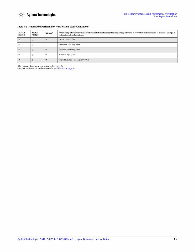
Post-Repair Procedures and Performance Verification Post Repair Procedures
? ? ? DCFM Carrier Offset
? ? Amplitude Switching Speed
? ? ? Frequency Switching Speed
? ? ? Timebase Aging Rate
? ? ? Internal Rise Fall Time (Option UNW)
aThe manual phase noise test is required as part of acomplete performance verification (refer to Table 4-3 on page 5).
Table 4-5 Automated Performance Verification Tests (Continued)
N5161A N5181A
N5162A N5182A
N5183Aa Automated performance verification tests are listed in the order they should be performed to prevent invalid results and to minimize changes in test equipment configurations.
Agilent Technologies N5161A/62A/81A/82A/83A MXG Signal Generators Service Guide 4-7

Post-Repair Procedures and Performance VerificationPerformance Verification
Performance VerificationThe procedures in this chapter verify the signal generators electrical performance.
• “I/Q Calibration (N5162A/82A only)” on page 4-8
• “Running Self Test” on page 4-8
• “Relative Frequency Range and Accuracy Verification (N5161A/62A1/81A/82A Only)” on page 4-10
• “Leveled Output Power Verification (N5161A/62A1/81A/82A Only)” on page 4-13
I/Q Calibration (N5162A/82A only)When you perform an I/Q calibration, that calibration data takes precedence over the factory-supplied calibration data. The calibration routines improves performance that may degrade over time or due to temperature changes.
Running Self Test
The self test is a series of internal tests of signal generator functions. Run the complete self tests when initially setting up a signal generator, after an assembly repair, or to verify signal generator performance. Also run self test prior to performing manual or automated Performance Verification tests. The self test will confirm the signal generator is operating properly or isolate problems to a specific faulty assembly.
Press I/Q > I/Q Calibration > Calibration Type Full
It takes about 5 minutes to run the self test.
This information is supplemental. Please disregard unless Agilent specifically requests this information.
Agilent Technologies N5161A/62A/81A/82A/83A MXG Signal Generators Service Guide 4-8

Post-Repair Procedures and Performance Verification Running Self Test
Use the following procedure to run the self test:
1. Disconnect all unnecessary1 external cables, including GPIB, LAN, and USB cables.
2. Preset the signal generator: Press Preset > Utility > Instrument Info > Self Test.
The following message appears:
• The current status of the self-test is: Incomplete. Not all tests have been run.
3. Press Run Complete Self Test.
An activity bar displays on the screen indicating the test progress.
When self-test completes, one of the following messages displays:
• The current status of the self-test is: Passed
• The current status of the self-test is: Failure. One or more tests have failed. System diagnostics indicate this test as the root failure: xxx
If the signal generator fails only one test, the title of the failed test displays. If the signal generator fails more than one test, the test number of the most significant failure displays.
Self Test Failure
1. Confirm that all unnecessary1 external cables, including GPIB, LAN, and USB cables, are disconnected from the signal generator and repeat the self-test.
2. If the self test continues to fail, the signal generator requires service. If you are unable to service the signal generator, send it to an Agilent service center for repair. Include a detailed description of the failed test(s) and any displayed error messages.
See “Viewing Test Results” on page 4-9 for information about viewing detailed self test results.
See “Returning a Signal Generator for Service” on page 1-2 for return instructions.
Viewing Test Results
If a self test fails the summary display indicates the probable cause.
To view the failed self test
1. Press: Utility > Instrument Info > Self Test > View Test Info
2. Use the arrow keys to highlight the desired test and press View Details.
NOTE This information is supplemental. Please disregard unless Agilent specifically requests the information.
1The N5161A/62A require a LAN or USB connection to access the Self Test softkeys via the Web-Enabled MXG. Refer to “Accessing the MXG Web-Enabled Page” on page 1-18.
Agilent Technologies N5161A/62A/81A/82A/83A MXG Signal Generators Service Guide 4-9

Post-Repair Procedures and Performance VerificationRelative Frequency Range and Accuracy Verification (N5161A/62A1/81A/82A Only)
Relative Frequency Range and Accuracy Verification (N5161A1/62A1/81A/82A Only)The frequency range is tested by determining the frequency accuracy relative to the timebase at the frequency limits of the signal generator. This test can be performed with either a frequency counter or a spectrum analyzer.
• “Frequency Counter Procedure (N5161A/62A/81A/82A)” on page 4-10 or
• “Spectrum Analyzer Procedure (N5161A/62A1/81A/82A)” on page 4-11
Frequency Counter Procedure (N5161A/62A/81A/82A)
Test Setup
1. Connect the equipment as shown.
2. Preset the signal generator: Press Preset.
3. Turn modulation off: Press the Mod On/Off so that the MOD On/Off LED turns off.
4. Set the amplitude: Press Amplitude and enter 0 dBm.
5. Turn RF on: Press RF On/Off so that the RF On/Off LED lights.
6. Verify that the frequency counter is locked to the 10 MHz external reference frequency (±1 Hz).
7. For maximum accuracy, set the gate time on the frequency counter to >5 seconds. (Press Gate & ExtArm twice and use the arrow keys to set the value.)
8. Set the frequency: Press Frequency and set the signal generator to the first frequency listed in Table 4-7.
9. Confirm that the measured frequency is within the limits listed.
10. Repeat step 8 and step 9 for all of the frequencies in the table that are within the frequency range of your signal generator.
NOTE For frequencies <200 MHz, use Channel 3 on the frequency counter (press Freq Ratio until CH3: displays).
1The N5161A/62A performs the identical internal tests as in the MXG via a LAN connection to a Web Server. The front panel displays all hardkeys, softkeys and test results as depicted in the illustration. For information on Web-Enabled Control refer to “Accessing the MXG Web-Enabled Page” on page 1-18 and to the Programming Guide.
Table 4-6 Recommended Equipment for Checking N5161A/62A/81A/82A Frequency Range and Accuracy
Test Equipment Recommended Model
Frequency Counter Agilent 53131A/32A Universal Counter
Agilent Technologies N5161A/62A/81A/82A/83A MXG Signal Generators Service Guide 4-10
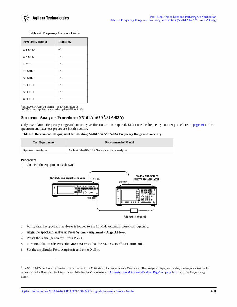
Post-Repair Procedures and Performance Verification Relative Frequency Range and Accuracy Verification (N5161A/62A1/81A/82A Only)
Spectrum Analyzer Procedure (N5161A1/62A1/81A/82A)
Only one relative frequency range and accuracy verification test is required. Either use the frequency counter procedure on page 10 or the spectrum analyzer test procedure in this section.
Procedure1. Connect the equipment as shown.
2. Verify that the spectrum analyzer is locked to the 10 MHz external reference frequency.
3. Align the spectrum analyzer: Press System > Alignment > Align All Now.
4. Preset the signal generator: Press Preset.
5. Turn modulation off: Press the Mod On/Off so that the MOD On/Off LED turns off.
6. Set the amplitude: Press Amplitude and enter 0 dBm.
Table 4-7 Frequency Accuracy Limits
Frequency (MHz) Limit (Hz)
0.1 MHza
aN5181A/82A with s/n prefix: < xx4740, measure at 0.25MHz (except instruments with options 099 or 01K).
±1
0.5 MHz ±1
1 MHz ±1
10 MHz ±1
50 MHz ±1
100 MHz ±1
500 MHz ±1
800 MHz ±1
1The N5161A/62A performs the identical internal tests as in the MXG via a LAN connection to a Web Server. The front panel displays all hardkeys, softkeys and test results
as depicted in the illustration. For information on Web-Enabled Control refer to “Accessing the MXG Web-Enabled Page” on page 1-18 and to the Programming
Guide.
Table 4-8 Recommended Equipment for Checking N5161A/62A/81A/82A Frequency Range and Accuracy
Test Equipment Recommended Model
Spectrum Analyzer Agilent E4440A PSA Series spectrum analyzer
Agilent Technologies N5161A/62A/81A/82A/83A MXG Signal Generators Service Guide 4-11
Post-Repair Procedures and Performance VerificationRelative Frequency Range and Accuracy Verification (N5161A/62A1/81A/82A Only)
7. Turn RF on: Press RF On/Off so that the RF On/Off LED lights.
8. Set the frequency: Press Frequency and set the signal generator to the first frequency listed in Table 4-9.
9. Confirm that the measured frequency is within the limits listed in Table 4-9.
10. Repeat step 8 and step 9 for all of the frequencies in the table that are within the frequency range of your signal generator.
Table 4-9 Frequency Accuracy Limits
Frequency (MHz) Limit (Hz)
0.1 MHza
aN5181A/82A with s/n prefix: < xx4740, measure at 0.25MHz (except instruments with options 099 or 01K).
±1
0.5 MHz ±1
1 MHz ±1
10 MHz ±1
50 MHz ±1
100 MHz ±1
500 MHz ±1
800 MHz ±1
1000 MHz ±1
2000 MHz ±1
3100 MHz ±1
4000 MHz ±1
5000 MHz ±1
6000 MHz ±1
Agilent Technologies N5161A/62A/81A/82A/83A MXG Signal Generators Service Guide 4-12

Post-Repair Procedures and Performance Verification Leveled Output Power Verification (N5161A/62A1/81A/82A Only)
Leveled Output Power Verification (N5161A1/62A1/81A/82A Only)This test verifies that the output power from the signal generator is within defined limits. The following table lists the preferred equipment for this test.
• “N5161A1/81A Output Power Test Procedure” on page 4-13
• “N5162A/82A Output Power Test Procedure” on page 4-15
N5161A1/81A Output Power Test Procedure1. Zero and calibrate the power sensor to the power meter:
2. Connect the equipment as shown:
3. Preset the signal generator: Press Preset.
4. Turn RF on: Press RF On/Off so that the RF On/Off LED lights.
5. Turn modulation off: Press Mod On/Off so that the Mod On/Off LED turns off.
6. Set the frequency: Press Frequency and enter the first frequency value listed in Table 4-10.
1The N5161A/62A performs the identical internal tests as in the MXG via a LAN connection to a Web Server. The front panel displays all hardkeys, softkeys and test results
as depicted in the illustration. For information on Web-Enabled Control refer to “Accessing the MXG Web-Enabled Page” on page 1-18 and to the Programming
Guide.
Test Equipment Recommended Model
Power Meter Agilent E4418B or E4419A/B E-Series power meter
Power Sensor, Input: Type-N (m)
Agilent E9304A
Table 4-10Leveled Output Power Limits
Frequency Limits (dB)
125 MHz < 0.6dB
275 MHz < 0.6dB
338 MHz < 0.6dB
425 MHz < 0.6dB
Agilent Technologies N5161A/62A/81A/82A/83A MXG Signal Generators Service Guide 4-13
Post-Repair Procedures and Performance VerificationLeveled Output Power Verification (N5161A/62A1/81A/82A Only)
7. Set the amplitude to 131 dBm:
Press Amplitude > 13 > dBm.
8. Configure the power meter for the measurement.
a. Press the Frequency Cal Fac button on the power meter.
b. Select a power meter channel (if applicable).
c. Use the arrow keys to enter the frequency at which to measure the power.
9. Measure the output power level.
10. Repeat steps 6 through 9 to measure power at each of the 15 frequencies listed in Table 4-10.
11. Confirm that the measured power levels are within the limits listed in the table.
NOTE The limit range is due to power meter uncertainty.
538 MHz < 0.6dB
675 MHz < 0.6dB
850 MHz < 0.6dB
1075 MHz < 0.6dB
1350 MHz < 0.6dB
1700 MHz < 0.6dB
2150 MHz < 0.6dB
2700 MHz < 0.6dB
3400 MHz < 0.7dB
4300 MHz < 0.8dB
5400 MHz < 0.8dB
1For serial numbers <MY4818xxxx, US4818xxxx, and SG4818xxxx, the amplitude = 7 dBm.
Table 4-10Leveled Output Power Limits (Continued)
Frequency Limits (dB)
Agilent Technologies N5161A/62A/81A/82A/83A MXG Signal Generators Service Guide 4-14

Post-Repair Procedures and Performance Verification Leveled Output Power Verification (N5161A/62A1/81A/82A Only)
N5162A1/82A Output Power Test Procedure1. Zero and calibrate the power sensor to the power meter:
2. Connect the equipment as shown below:
3. Preset the signal generator: Press Preset.
4. Select the factory-supplied waveform SINE_TEST_WFM:
a. Press Mode > Dual ARB > Select Waveform.
b. Highlight the SINE_TEST_WFM waveform.
c. Press Select Waveform.
5. Turn the arbitrary waveform player on: Press the ARB softkey to highlight On.
6. Turn RF on: Press RF On/Off so that the RF On/Off LED lights.
7. Verify modulation is off:
Press Mod On/Off so that the Mod On/Off LED turns off.
8. Set the signal generator frequency to the first value listed in Table 4-11:
Press Frequency > 338 > MHz.
1The N5161A/62A performs the identical internal tests as in the MXG via a LAN connection to a Web Server. The front panel displays all hardkeys, softkeys and test results
as depicted in the illustration. For information on Web-Enabled Control refer to “Accessing the MXG Web-Enabled Page” on page 1-18 and to the Programming
Guide.
Table 4-11Leveled Output Power Relative to
Frequency (MHz)
Limit Δ(dB)
338 0.25dB
425 0.25dB
538 0.25dB
675 0.25dB
850 0.25dB
1075 0.25dB
1350 0.25dB
1700 0.25dB
Agilent Technologies N5161A/62A/81A/82A/83A MXG Signal Generators Service Guide 4-15

Post-Repair Procedures and Performance VerificationLeveled Output Power Verification (N5161A/62A1/81A/82A Only)
9. Set the amplitude to 131 dBm:
Press Amplitude > 13 > dBm.
10. Configure the power meter as follows:
a. On the power meter, press the Frequency Cal Fac button.
b. If applicable, select a power meter channel.
c. Use the arrow keys to enter the frequency at which to measure the power.
11. Measure the output power level and write down the value.
12. Turn modulation on.
Press Mod On/Off so that the Mod On/Off LED turns on.
13. Measure the output level and write down the value.
14. Compare the values from step 11 and step 13. The Δ should be equal to or less than the test limit in Table 4-11.
15. Repeat steps 8 through 14 for the remaining frequencies in the table, confirm that the delta power level at each point is within limits.
2150 0.25dB
3400 0.25dB
5400 0.25dB
1For serial numbers <MY4818xxxx, US4818xxxx, and SG4818xxxx, the amplitude = 7 dBm.
Table 4-11Leveled Output Power Relative to (Continued)
Frequency (MHz)
Limit Δ(dB)
Agilent Technologies N5161A/62A/81A/82A/83A MXG Signal Generators Service Guide 4-16

5 Safety and Regulatory
This chapter provides information on the following:
• “General Safety Considerations” on page 5-1
• “Lithium Battery Disposal” on page 5-2
• “Assistance” on page 5-2
• “Certification” on page 5-2
The following safety notes are used throughout this manual. Familiarize yourself with each of the notes and its meaning before operating this instrument.
WARNING Warning denotes a hazard. It calls attention to a condition or situation that could result in personal injury or loss of life. Do not proceed beyond a warning until you fully understand the indicated conditions or situations.
CAUTION Caution calls attention to a condition or situation that could result in damage to or destruction of the signal generator, or in the loss of a user’s settings or data. Do not proceed beyond a caution until you fully understand the indicated conditions..
General Safety ConsiderationsThe following safety notes apply specifically to signal generators. These notes also appear in other chapters of this service guide as required.
WARNING These servicing instructions are for use by qualified personal only. To avoid electrical shock, do not perform any servicing unless you are qualified to do so.
WARNING The opening of covers or removal of parts is likely to expose dangerous voltages. Disconnect the product from all voltage sources before starting to open.
WARNING The detachable power cord is the instrument disconnecting device. It disconnects the main circuits from the main supply before other parts of the instrument. The front panel switch is only a standby switch and is not a LINE switch (disconnecting device).
WARNING The power cord is connected to internal capacitors that may remain live for 5 seconds after disconnecting the plug from its power supply.
WARNING This is a Safety Class 1 Product (provided with a protective earthing ground incorporated in the power cord). The mains plug shall only be inserted in a socket outlet provided with a protective earth contact. Any interruption of the protective conductor inside or outside of the product is likely to make the product dangerous. Intentional interruption is prohibited.
WARNING Replace battery only with the same or equivalent type recommended. Discard used batteries according to manufacturer’s instructions.
WARNING If this product is not used as specified, the protection provided by the equipment could be impaired. This product must be used in a normal condition (in which all means for protection are intact) only.
CAUTION Many of the assemblies in this instrument are very susceptible to damage from electrostatic discharge (ESD). Perform service procedures only at a static-safe workstation and wear a grounding strap.
Agilent N5161A/62A/81A/82A/83A MXG Signal Generators Service Guide 5- 1

Safety and RegulatoryLithium Battery Disposal
Lithium Battery DisposalWhen the battery on the A14 CPU is exhausted and/or ready for disposal, dispose of it according to your country’s requirements. You can return the battery to your nearest Agilent Technologies Sales and Service office for disposal, if required.
Figure 5-1
AssistanceProduct maintenance agreements and other customer assistance agreements are available for Agilent Technologies products. For any assistance, contact your nearest Agilent Technologies sales and service office.
CertificationAgilent Technologies Company certifies that this product met its published specifications at the time of shipment from the factory. Agilent Technologies further certifies that its calibration measurements are traceable to the United States National Institute of Standards and Technology, to the extent allowed by the Institute’s calibration facility, and to the calibration facilities of other International Standards Organization members.
Agilent N5161A/62A/81A/82A/83A MXG Signal Generators Service Guide
5-2

6 Instrument History
How to Use this ChapterThis chapter documents changes that have been made to the N518xA signal generators. If your signal generator is an early version these changes may affect it.
September 2009 Initial release of Option R2C. For more information on Option R2C, refer to www.agilent.com.
• Firmware release A.01.60
• Added internal channel flatness correction to N5162A and N5182A.
• Enabled the use of “SOCK” in SCPI commands that use “SOCKETS”.
January 2009 (N5161A/62A/81A/82A/83A only)Initial release of Agilent Upgrade License (AUS). For more information on AUS, refer to www.agilent.com.
• Firmware release A.01.50
August 2008 (N5161A/62A/81A/82A/83A only)• Firmware release A.01.44
April 2008 (N5182A/83A only)• New 4 GB A4 Internal Memory Card
December 2007Initial release of the N5183A MXG Microwave Analog Signal Generator.
• Serial prefix US/MY/SG4742
• Firmware release A.01.32
• A1 Power Supply updated to 400 Hz capability.
• N5183A specific A3 RF Assembly, part number N5180-60077.
November 2007• Firmware release A.01.31
• Implemented rear panel pulse output polarity selection when pulse is off.
• Added user flatness correction when using an external power meter/sensor.
• Improved error checking and error messages
October 2007 (N5181A/82A only)• Serial prefix US/MY/SG4740
• Firmware release A.01.24
• Performance specified to 100 kHz.
• Release of Option UNW High Performance Pulse Modulation.
• Disabled DAC over range protection to provide higher dynamic range when using Runtime Scaling.
• A3 RF Assembly part number N5180-60099
May 2007 (N5181A/82A only)• Serial prefix US/MY/SG4707
Agilent N5161A/62A/81A/82A/83A MXG Signal Generators Service Guide 6- 1

Instrument History
• Firmware release A.01.20
• 43x Options introduced.
• Five Pack licensing available.
• Release of upgradeable internal BBG maximum sample rate.
• Softkeys for “Int Phase Polarity” and “Burst Envelope” added.
• A3 RF Assembly part number N5180-60076
December 2006 (N5181A/82A only)• Firmware release A.01.10
• Compatibility languages for Agilent, Aeroflex, IFR, and Rhonde&Schwartz signal generators released.
• Option and license file backup locations on the A3 RF Assembly and the A5 CPU implemented.
• A3 RF Assembly part number N5180-60065
September 2006 (N5181A/82A only)Initial release of the N5181A/82A MXG Signal Generators.
• Serial prefix US/MY/SG4624
• Firmware release A.01.04
• A3 RF Assembly part number N5180-60001
Agilent N5161A/62A/81A/82A/83A MXG Signal Generators Service Guide 6-2

Index
Numerics6 GHz electronic attenuator, troubleshooting, 1-68
AA2 Vector Module (N5182A 1EM with Option 012), 3-30A3 RF Assembly - N5182A Option 1EM (with and without Option 012), 3-34A3 RF Assembly - N5182A with Option 012, 3-34adjustments (n5183a only), 3-6Agilent Technologies, contacting, 1-2Agilent Technologies, returning signal generator to, 1-2antistatic materials, 2-29assemblies list, 2-3assembly replacement
A1 Power Supply, 3-28A2 Vector Module (N5162A with Option 012), 3-30A2 Vector Module (N5162A/82A without Option 012), 3-32A3 RF Assembly - N5161A and N5181A Option 1EM, 3-42A3 RF Assembly - N5162A(with and without Option 012), 3-34A3 RF Assembly - Standard (N5181A/82A), 3-38A3 RF Assembly (N5183A), 3-46A3BT1 Battery, 3-50A4 Internal Memory Card, 3-52A5 CPU, 3-54A6 DC-AC Inverter Interface Board, 3-16, 3-18, 3-56, 3-59A7 Micro-Deck, 3-56, 3-59A8 Floating BNC Bypass, 3-62A9 Interface Board, 3-18B1 thru B4 Fan, 3-66Front-Panel, 3-10Inner Bottom Cover, 3-8Inner Top Cover, 3-6Key Pad, 3-20LCD Display, 3-14Outer Cover, 3-4Power Switch, 3-21Rear Panel (N5181A), 3-22Rear Panel (N5182A), 3-24Rear Panel (N5183A), 3-26USB Board, 3-12, 3-64
automated performance tests, 3-6
Bbattery, replacement, 3-50before you replace an assembly, 3-1
Ccables, 2-14CPU, replacement, 3-54
Ddc-ac inverter interface board, replacement, 3-16, 3-18, 3-56, 3-59disclaimer
LXI-B, 1-18Display, 3-14
Eelectrostatic discharge supplies, 2-29
Ffailure
self-test, 3-9
fan, replacement, 3-66floating BNC bypass, replacement, 3-62frequency accuracy check, 3-10frequency range and accuracy check, 3-10front-panel, replacement, 3-10
Hhardware, 2-21hardware list, 2-3
II/Q calibration (n5183a only), 3-8inner bottom cover, replacement, 3-8inner top cover, replacement, 3-6Install Assembly softkey, 3-2instrument history, 6-1interface board, replacement, 3-18internal memory card, replacement, 3-52
Kkey pad, replacement, 3-20
Llcd display, replacement, 3-14lists
assemblies and hardware options, 2-3cables, 2-14hardware, 2-21replaceable assemblies, 3-1
lithium batterydisposal, 4-2replacement, 3-50
LXI-Bdisclaimer, 1-18
Mmanual performance tests, 3-4micro-deck, replacement, 3-56, 3-59MXG ATE
web-enabled, accessing, 1-18
Ooptions, descriptions, 2-2outer cover, replacement, 3-4output power, checking, 3-13
Pperformance tests
automated, 3-6manual, 3-4
performance tests, required after repair, 3-1performance tests, troubleshooting, 1-72post-repair overview, 3-4post-repair procedures, 3-1power
checking, 3-13power supply, replacement, 3-28power switch, replacement, 3-21
Rrear panel (N5181A), replacement, 3-22
I- 1

rear panel (N5182A), replacement, 3-24rear panel (N5183A), replacement, 3-26Remove Assembly softkey, 3-2repair
performance tests required, 3-1replaceable parts
assemblies, 3-1cables, 2-14hardware, 2-21ordering information, 2-1
rf assembly, replacement, 3-34, 3-38, 3-42, 3-46RF path, troubleshooting, 1-66, 1-68
Ssafety, general considerations, 4-1self-test failure, 3-9self-tests, 3-8
overview, 1-15running, 1-16
signal generator, returning to Agilent Technologies, 1-2
Ttroubleshooting, 1-1troubleshooting output power, 3-13troubleshooting, 6 GHz electronic attenuator, 1-68
Uunlevels, troubleshooting, 1-66, 1-68unlocks, troubleshooting, 1-65USB board, replacement, 3-12, 3-64Utility softkey, 3-2
Vvector module, replacement, 3-30, 3-32
I- 2


![AKT4U - 82a[1]](https://static.fdocuments.net/doc/165x107/55295c2a550346522e8b4741/akt4u-82a1.jpg)


![Agilent Technologies N5161A/62A/81A/82A/83A MXG Signal ...literature.cdn.keysight.com/litweb/pdf/N5180-90004.pdf · Contents vi Agilent N5161A/62A/81A/82A/83A SCPI Command Reference:MARKer[0,1,2,3,4,5,6,7,8,9,10,11,12,13,14,15,16,17,18,19]:FREQuency](https://static.fdocuments.net/doc/165x107/60175464f4f7d147d01bdb0d/agilent-technologies-n5161a62a81a82a83a-mxg-signal-contents-vi-agilent-n5161a62a81a82a83a.jpg)


