N+1 and Oring Power Rail Controller with Enable (Rev. B) · PDF fileC A GND GATE Voltage...
27
C A GND GATE Voltage Source C BYP BYP RSET RSVD R SET Common Voltage Rail EN Enable R2 R1 TPS2419 www.ti.com SLVS998B – FEBRUARY 2010 – REVISED SEPTEMBER 2011 N+1 and ORing Power Rail Controller with Enable Check for Samples: TPS2419 1FEATURES • Control External FET for N+1 and ORing DESCRIPTION • Controls Buses From 3 V to 16.5 V The TPS2419 controller, in conjunction with an • External Enable external N-channel MOSFET, provides the reverse current protection of an ORing diode with the • N-Channel MOSFETControl efficiency of a MOSFET. The TPS2419 can be used • Rapid Device Turnoff Protects Bus Integrity to combine multiple power supplies to a common bus • Programmable Turn-Off Threshold in an N+1 configuration, or to combine redundant input power buses. • Soft Turn on Reduces Bus Transients • Industrial Temperature Range: –40°C to 85°C Applications for the TPS2419 include a wide range of systems including servers and telecom. These • 8-Pin TSSOP and SOIC Packages applications often have either N+1 redundant power supplies, redundant power buses, or both. Redundant APPLICATIONS power sources must have the equivalent of a diode • N+1 Power Supplies OR to prevent reverse current during faults and hotplug. • Server Blades • Telecom Systems Accurate voltage sensing and a programmable turn-off threshold allows operation to be tailored for a • High Availability Power Modules wide range of implementations and bus characteristics. The TPS2419 brings out an enable pin which allows the system to force the MOSFET off under light-load, high noise conditions. Table 1. Family Features ' 2410 ' 2411 ' 2412 ' 2413 ' 2419 Enable input √ √ √ Linear gate control √ √ ON/OFF gate √ √ √ control Turnoff √ √ comparator filtering Voltage monitoring √ √ MOSFET fault √ √ monitoring Status pin √ √ Independent √ √ √ √ Supply Pin Figure 1. Typical Application 1 Please be aware that an important notice concerning availability, standard warranty, and use in critical applications of Texas Instruments semiconductor products and disclaimers thereto appears at the end of this data sheet. PRODUCTION DATA information is current as of publication date. Copyright © 2010–2011, Texas Instruments Incorporated Products conform to specifications per the terms of the Texas Instruments standard warranty. Production processing does not necessarily include testing of all parameters.
Transcript of N+1 and Oring Power Rail Controller with Enable (Rev. B) · PDF fileC A GND GATE Voltage...

CA
GN
DG
AT
E
Volta
ge
Sourc
e
CB
YP
BY
PR
SE
T
RS
VD
RS
ET
Com
mon
Volta
ge
Rail
EN
EnableR
2R
1
TPS2419
www.ti.com SLVS998B –FEBRUARY 2010–REVISED SEPTEMBER 2011
N+1 and ORing Power Rail Controller with EnableCheck for Samples: TPS2419
1FEATURES• Control External FET for N+1 and ORing DESCRIPTION• Controls Buses From 3 V to 16.5 V The TPS2419 controller, in conjunction with an• External Enable external N-channel MOSFET, provides the reverse
current protection of an ORing diode with the• N-Channel MOSFETControlefficiency of a MOSFET. The TPS2419 can be used• Rapid Device Turnoff Protects Bus Integrity to combine multiple power supplies to a common bus
• Programmable Turn-Off Threshold in an N+1 configuration, or to combine redundantinput power buses.• Soft Turn on Reduces Bus Transients
• Industrial Temperature Range: –40°C to 85°C Applications for the TPS2419 include a wide range ofsystems including servers and telecom. These• 8-Pin TSSOP and SOIC Packagesapplications often have either N+1 redundant powersupplies, redundant power buses, or both. RedundantAPPLICATIONSpower sources must have the equivalent of a diode
• N+1 Power Supplies OR to prevent reverse current during faults andhotplug.• Server Blades
• Telecom Systems Accurate voltage sensing and a programmableturn-off threshold allows operation to be tailored for a• High Availability Power Moduleswide range of implementations and buscharacteristics. The TPS2419 brings out an enablepin which allows the system to force the MOSFET offunder light-load, high noise conditions.
Table 1. Family Features
'2410 '2411 '2412 '2413 '2419
Enable input √ √ √
Linear gate control √ √
ON/OFF gate √ √ √control
Turnoff √ √comparatorfiltering
Voltage monitoring √ √
MOSFET fault √ √monitoring
Status pin √ √
Independent √ √ √ √Supply Pin
Figure 1. Typical Application
1
Please be aware that an important notice concerning availability, standard warranty, and use in critical applications of TexasInstruments semiconductor products and disclaimers thereto appears at the end of this data sheet.
PRODUCTION DATA information is current as of publication date. Copyright © 2010–2011, Texas Instruments IncorporatedProducts conform to specifications per the terms of the TexasInstruments standard warranty. Production processing does notnecessarily include testing of all parameters.

TPS2419
SLVS998B –FEBRUARY 2010–REVISED SEPTEMBER 2011 www.ti.com
This integrated circuit can be damaged by ESD. Texas Instruments recommends that all integrated circuits be handled withappropriate precautions. Failure to observe proper handling and installation procedures can cause damage.
ESD damage can range from subtle performance degradation to complete device failure. Precision integrated circuits may be moresusceptible to damage because very small parametric changes could cause the device not to meet its published specifications.
PRODUCT INFORMATION (1)
MOSFET GATEDEVICE TEMPERATURE PACKAGE (1) MARKINGCONTROL
PW (TSSOP-8) 2419TPS2419 –40°C to 85°C ON/OFF
D (SO-8) 2419D
(1) For package and ordering information, see the Package Option Addendum at the end of thisdocument, or see the TI Web site at www.ti.com.
ABSOLUTE MAXIMUM RATINGS (1)
over recommended operating junction temperature range, voltages are referenced to GND (unless otherwise noted)
VALUE UNIT
A, C voltage –0.3 to 18 V
A above C voltage 7.5 V
C above A voltage 18 V
GATE, BYP voltage (2) –0.3 to 30 V
BYP to A voltage –0.3 to 13 V
GATE above BYP voltage 0.3 V
RSET (2) voltage –0.3 to 7 V
EN –0.3 to 5.5 V
GATE short to A or C or GND Indefinite
Human body model 2 kVESD
Charged device model 500 V
TJ Maximum junction temperature Internally limited °C
(1) Stresses beyond those listed under absolute maximum ratings may cause permanent damage to the device. These are stress ratingsonly and functional operation of the device at these or any other conditions beyond those indicated under recommended operatingconditions is not implied. Exposure to absolute-maximum-rated conditions for extended periods may affect device reliability.
(2) Voltage should not be applied to these pins.
DISSIPATION RATINGSPOWER RATING
PACKAGE θJA – Low k °C/W θJA – High k °C/W High kTA = 85°C (mW)
PW (TSSOP) 258 159 250
D (SO) 176 97.5 410
2 Copyright © 2010–2011, Texas Instruments Incorporated
Product Folder Link(s): TPS2419

TPS2419
www.ti.com SLVS998B –FEBRUARY 2010–REVISED SEPTEMBER 2011
RECOMMENDED OPERATING CONDITIONSvoltages are referenced to GND (unless otherwise noted)
MIN NOM MAX UNIT
A, C Input voltage range (1) 0 16.5 V
A to C Operational voltage 5 V
EN Input voltage range 0 5 V
R(RSET) Resistance range (2) 1.5 ∞ kΩC(BYP) Capacitance Range (2) 800 2200 10k pF
TJ Operating junction temperature –40 125 °C
(1) V(C) must exceed 2.5 V for normal operation and 3 V to meet gate drive specification(2) Voltage should not be applied to these pins.
ELECTRICAL CHARACTERISTICS (1)
Common conditions (unless otherwise noted) are: [3 V ≤ ( V(A), V(C) ) ≤ 18 V ] , C(BYP) = 2200 pF, R(RSET) = open, EN = 2 V,GATE = open, –40°C ≤ TJ ≤ 125°C, positive currents into pins, typical values are at 25°C, all voltages with respect to GND.
PARAMETER TEST CONDITIONS MIN TYP MAX UNIT
A, C
V(C) rising 2.25 2.5Supply UVLO V
Hysteresis 0.25
| I(A) |, Gate in active region 0.66 1A current mA
| I(A) |, Gate saturated high 0.1
Worst case, gate in active region, V(AC) ≤ 0.1 V 4.25 6C current mA
Gate saturated high, V(AC) ≤ 0.1 V 1.2
EN
Threshold voltage V(EN) rising 1.25 1.3 1.35 V
Hysteresis 29 mV
V(AC) = 0.1 V, V(EN)↑ : 1.1 V → 1.4 V, measure 0.65 1period to V(GATE) = 0.25 VResponse time μs
V(AC) = 0.1 V, V(EN)↓: 1.4 V → 1.1 V, measure 0.3 0.6period to V(GATE) = V(ON) - 0.25 V
Leakage current (source or sink) V(EN) = 0.5 V 1 μA
TURN ON
Forward turn-on voltage - VON V(A-C) 58 65 71 mV
TURN OFF
Gate sinks > 10 mA at V(GATE-A) = 2 V
V(A-C) falling, R(RSET) = open 1 3 5Turn-off threshold voltage mV
V(A-C) falling, R(RSET) = 28.7 kΩ -17 -13.25 -10
V(A-C) falling, R(RSET) = 3.24 kΩ -170 -142 -114
V(A) = 12 V, V(A-C): 20 mV → –20 mV,Turn-off delay 70 nsV(GATE-A) begins to decrease
V(A) = 12 V, C(GATE-GND) = 0.01 μF, V(A-C):Turn-off time 20 mV → –20 mV, measure the period to 130 ns
V(GATE) = V(A)
(1) Parameters with only typical values are provided for reference only, and do not constitute part of TI's published device specifications forpurposes of TI's product warranty.
Copyright © 2010–2011, Texas Instruments Incorporated 3
Product Folder Link(s): TPS2419

+
-
+
-
A
GATE
Charge Pump
and Bias Supply
VDD
Bias and
ControlVDD
HVUV
en
HVUV
Thermal Shutdown
(135ºC)
VBIAS
0.5V
RSET
10VA
BYP
C
GND
3mV
en
RSVD
en
TURNOFF
COMP.
TURNONCOMP.
VDD
1.3V
EN
S
R
Q
Q
en
MULTISTAGEPULLDOWN
C
+-
+ -
+-
VON
TPS2419
SLVS998B –FEBRUARY 2010–REVISED SEPTEMBER 2011 www.ti.com
ELECTRICAL CHARACTERISTICS(1) (continued)Common conditions (unless otherwise noted) are: [3 V ≤ ( V(A), V(C) ) ≤ 18 V ] , C(BYP) = 2200 pF, R(RSET) = open, EN = 2 V,GATE = open, –40°C ≤ TJ ≤ 125°C, positive currents into pins, typical values are at 25°C, all voltages with respect to GND.
PARAMETER TEST CONDITIONS MIN TYP MAX UNIT
GATE
V(C) = 3 V, V(A-C) = 200 mV 6 7 8Gate positive drive voltage, V(GATE-A) V
5 V ≤ VC ≤ 18 V, V(A-C) = 200 mV 9 10.2 11.5
Gate source current V(A-C) = 200 mV, V(GATE-A) = 4 V 250 290 350 μA
V(A-C) = –0.1 V
V(GATE) = 8 V 1.75 2.35 ATurn-off pulsed current, I(GATE)
V(GATE) = 5 V 1.25 1.75
Period 7.5 12.5 μs
V(A-C) = –0.1 V, 3 V ≤ VC ≤ 18 V,Sustain turn-off current, I(GATE) 15 19.5 mA2 V ≤ V(GATE) ≤ 18 V
MISCELLANEOUS
Thermal shutdown temperature Temperature rising, TJ 135 °CThermal hysteresis 10 °C
FUNCTIONAL BLOCK DIAGRAM
4 Copyright © 2010–2011, Texas Instruments Incorporated
Product Folder Link(s): TPS2419

A
GND
RSVD
BYP
C
GATE
1
4
8RSET
EN
5
TPS2419
www.ti.com SLVS998B –FEBRUARY 2010–REVISED SEPTEMBER 2011
PW and D PACKAGE(TOP VIEW)
TERMINAL FUNCTIONSTERMINAL
I/O DESCRIPTIONNAME NO.
Connect a resistor to ground to program the turn-off threshold. Leaving RSET open results in a slightlyRSET 1 I positive V(A-C) turn-off threshold.
EN 2 I Pull EN above 1.3 V to permit normal ORing operation. A low on EN holds GATE low.
RSVD 3 PWR This pin must be connected to GND.
GND 4 PWR Device ground.
GATE 5 O Connect to the gate of the external MOSFET. Controls the MOSFET to emulate a low forward-voltage diode.
Voltage sense input that connects to the simulated diode cathode, and also serves as the bias supply for theC 6 I gate drive charge pump and internal controls. Connect to the MOSFET drain in the typical configuration.
Voltage sense input that connects to the simulated diode anode, and also serves as the reference for theA 7 I charge-pump bias supply on BYP. Connect to the MOSFET source in the typical configuration.
BYP 8 I/O Connect a capacitor from BYP to A to filter the gate drive supply voltage.
Copyright © 2010–2011, Texas Instruments Incorporated 5
Product Folder Link(s): TPS2419

-470.02R(RSET)
V - 0.00314(OFF)
æ öç ÷=ç ÷è ø
TPS2419
SLVS998B –FEBRUARY 2010–REVISED SEPTEMBER 2011 www.ti.com
DETAILED DESCRIPTION
The following descriptions refer to the pinout and the functional block diagram.
A, C: The A pin serves as the simulated diode anode and the C as the cathode. GATE is driven high when V(A-C)exceeds 65 mV. A strong GATE pull-down is applied when V(A-C) is less than the programmable turn-off threshold(see RSET). These two thresholds serve as a hysteretic GATE control with the ON/OFF state preserved until thenext (opposite) threshold cross.
The internal charge pump output, which provides bias power to the comparators and voltage to drive GATE, isreferenced to A. Some charge pump current appears on A.
C is both the cathode voltage sense and the bias supply for the gate-drive charge pump and other internalcircuits. This pin must be connected a source that is 3 V or greater when the external MOSFET is to be turnedon.
A 0.01-μF minimum bypass capacitor to GND is recommended for both A and C inputs. A and C connections tothe bypass capacitor and the controlled MOSFET should be short and low impedance.
The inputs are protected from excess differential voltage by a clamp diode and series resistance. If C falls belowA by more than about 0.7 V, a small current flows out of C. Configurations which permit C to be more than 6 Vlower than A should be avoided.
BYP: BYP is the internal charge pump output, and the positive supply voltage for internal comparator circuits andGATE driver. A capacitor must be connected from BYP to A. While the capacitor value is not critical, a 2200-pFceramic is recommended. Traces to this part must be kept short and low impedance to provide adequate filtering.Shorting this pin to a voltage below A damages the TPS2419.
EN: A voltage greater than 1.3 V on EN permits the TPS2419 to operate in its normal ORing mode. A voltagebelow the lower threshold forces GATE to remain low, however EN going high will not automatically turn GATEON. EN going low when GATE is high engages the sustain current pulldown. EN should not be driven higherthan its recommended maximum voltage.
GATE: Gate controls the external N channel MOSFET gate. GATE is driven positive with respect to A by a driveroperating from the voltage on BYP. A time-limited high current discharge source pulls GATE to GND when theturn-off comparator is activated. The high-current discharge is followed by a sustaining pull-down. The turn-offcircuits are disabled by the thermal shutdown, leaving a resistive pull-down to keep the gate from floating. Thegate connection should be kept low impedance to maximize turn-off current.
GND: This is the input supply reference. GND should have a low impedance connection to the ground plane. Itcarries several Amperes of rapid-rising discharge current when the external MOSFET is turned off, and alsocarries significant charge pump currents.
RSET: A resistor connected from this pin to GND sets the V(A-C) turn-off comparator threshold. The threshold isslightly positive when the RSET pin is left open. Current drawn by the resistor programs the turn-off voltage toincreasing negative values. The TPS2419 must have a negative threshold programmed to avoid an unstablecondition at light load. The expression for R(RSET) in terms of the turn-off voltage ( V(OFF)= V(A) - V(C)) follows.
(1)
The units of the numerator are (V × V/A). V(OFF) is positive for V(A) greater than V(C), V(OFF) is less than 3 mV, andR(RSET) is in ohms.
RSVD: Connect to ground.
6 Copyright © 2010–2011, Texas Instruments Incorporated
Product Folder Link(s): TPS2419

0.5
1.5
2.0
2.5
3.0
0 2 4 6 8 10I (
GA
TE
)−
A
V − V(GATE - GND)
1.0
0.0
T = 125 CJo
T = 85 CJo
T = 25 CJo
T = -40 CJo
R = Open(RSET)
1.5
2.5
3.5
4.5
5.0
−40 −20 0 20 40 60 80 100 120
V(A
C)
−m
V
T − Junction TJ emperature − Co
4.0
3.0
2.0
1.0
T = 125 CJo
T = 25 CJo
T = -40 CJo
10
20
40
50
60
2 4 6 8 10 12 14 16 18
De
lay
−s
m
V − VDD
30
0
T = -40 CJo
T = 125 CJo
T = 25 CJo
0.5
1.0
2.0
2.5
3.0
2 4 6 8 10 12 14 16 18
I (V
DD
)−
mA
V − VC
1.5
0.0
TPS2419
www.ti.com SLVS998B –FEBRUARY 2010–REVISED SEPTEMBER 2011
TYPICAL CHARACTERISTICSTURNOFF THRESHOLD PULSED GATE SINKING CURRENT
vs vsTEMPERATURE GATE VOLTAGE
Figure 2. Figure 3.
TURNON DELAY I(C)vs vs
V(C) V(C)(POWER APPLIED UNTIL GATE IS ACTIVE) (GATE SATURATED HIGH)
Figure 4. Figure 5.
Copyright © 2010–2011, Texas Instruments Incorporated 7
Product Folder Link(s): TPS2419

1.25
1.26
1.27
1.28
1.29
1.3
1.31
1.32
-40 -20 0 20 40 60 80 100 120T - Junction Temperature - °CJ
EN Hysteresis ~ 29 mV
EN Rising
EN Falling
EN
- T
hre
sh
old
- V
64.5
64.6
64.7
64.8
64.9
65
65.1
65.2
65.3
65.4
65.5
-40 -20 0 20 40 60 80 100 120
T - Temperature - °CJ
V-
mV
ON
Time 1ms/DIV
GATE drives 10 nF to GND
V = 12 V, R = 61.9 WC SET WVA-C
Turn offThreshold
VGATE
Turn onThreshold
10 V
/DIV
20 m
v/D
IV
TPS2419
SLVS998B –FEBRUARY 2010–REVISED SEPTEMBER 2011 www.ti.com
TYPICAL CHARACTERISTICS (continued)TURN ON VOLTAGE ENABLETHRESHOLD
vs vsTEMPERATURE TEMPERATURE
Figure 6. Figure 7.
EXAMPLE TURNON AND TURNOFF
Figure 8.
8 Copyright © 2010–2011, Texas Instruments Incorporated
Product Folder Link(s): TPS2419

Time 100ns/DIV
GATE drives 10 nF to GND
V = 12 V, R = 61.9 WC SET W
VA-C
VGATE
V = VGATE A
Turn offThreshold
135 ns
IGATE
10
V/D
IV1
A/D
IV2
0 m
v/D
IV
TPS2419
www.ti.com SLVS998B –FEBRUARY 2010–REVISED SEPTEMBER 2011
TYPICAL CHARACTERISTICS (continued)EXAMPLE TURNOFF
Figure 9.
Copyright © 2010–2011, Texas Instruments Incorporated 9
Product Folder Link(s): TPS2419

V(AC)
V(G
AT
E)
VO
NGateON
GateOFF
3m
V
ProgrammableFast Turn-off
Threshold Range
TPS2419
SLVS998B –FEBRUARY 2010–REVISED SEPTEMBER 2011 www.ti.com
APPLICATION INFORMATION
OVERVIEW
The TPS2419 is designed to allow an output ORing in N+1 power supply applications (see Figure 11), and aninput-power bus ORing in redundant source applications (see Figure 12). The TPS2419 and external MOSFETemulate a discrete diode to perform this unidirectional power combining function. The advantage to thisemulation is lower forward voltage drop and higher efficiency.
The TPS2419 turns the MOSFET on and off like a comparator with hysteresis as shown in Figure 10. GATE isdriven high when V(A-C) exceeds 65 mV, and driven low if V(A-C) falls below the RSET programmed turn-offthreshold. Operation of the TPS2419 is demonstrated in Figure 8 where an ac-coupled square wave is appliedfrom A to C. Figure 8 shows the condition where the MOSFET gate is initially at GND, and V(A-C) is less than 65mV. When the turn-on threshold is exceeded, the TPS2419 turns on the MOSFET gate, and charges it to V(BYP).The gate stays high even though V(A-C) is less than the turn-on threshold. The TPS2419 pulls the gate to GNDwhen V(A-C) falls below the turn-off threshold.
System designs should account for the inherent delay between a TPS2419 circuit becoming forward biased, andthe MOSFET actually turning ON. The delay is the result of the MOSFET gate capacitance charge from groundto its threshold voltage by the 290 μA gate current. If there are no additional sources holding a common ORedrail voltage up, the MOSFET internal diode will conduct and maintain voltage on the ORed output. The ORedinput supply will experience a momentary large current draw as the MOSFET turns on, shorting the internal diodeand charging the bus capacitance.
Figure 10. TPS2419 Operation
The operation of the TPS2419 is summarized in Table 2.
Table 2. Operation as a Function of V(AC)
V(A-C) ≤ Turnoff Threshold (1) Turnoff Threshold (1) ≤ V(A-C) ≤ 65 mV V(A-C) > 65 mV
Depends on previous state (1)TPS2419 Gate pulled to GND GATE pulled high (ON)(Hysteresis region)
(1) Turnoff threshold is established by the value of RSET.
N+1 POWER SUPPLY – TYPICAL CONNECTION
The N+1 power supply configuration shown in Figure 11 is used where multiple power supplies are paralleled foreither higher capacity, redundancy or both. If it takes N supplies to power the load, adding an extra identical unitin parallel permits the load to continue operation in the event that any one of the N supplies fails. The suppliesare ORed together, rather than directly connected to the bus, to isolate the converter output from the bus when itis plugged-in or fails short. Thus, the TPS2419 with an external MOSFET emulates the function of the ORingdiode.
ORed supplies are usually designed to share power by various means, although the desired operation couldimplement an active and standby concept. Sharing approaches include both passive, or voltage droop, andactive methods. Not all of the output ORing devices may be ON depending on the sharing control method, busloading, distribution resistances, and tolerances.
10 Copyright © 2010–2011, Texas Instruments Incorporated
Product Folder Link(s): TPS2419
Co
mm
on
Bu
s
Concept
EN
A C
GN
DG
AT
E
Po
we
rC
on
ve
rsio
nB
lock
InputVoltage
PowerBus
Implementation
CB
YP
BY
P
DC/DC
Converter
DC/DC
Converter
RS
VD
EN
A C
GN
DG
AT
E
LOAD
Implementation
BY
P
A C
GN
DG
AT
EBU
S1
BU
S2
BackplanePower Buses
CB
YP
CB
YP
BY
P
Plug-In Unit
Common
Buses
Concept
HotswapDC/DC
Converter
EN
TPS2419
www.ti.com SLVS998B –FEBRUARY 2010–REVISED SEPTEMBER 2011
Figure 11. N+1 Power Supply Example
INPUT ORing – TYPICAL CONNECTION
Figure 12 shows how redundant buses may be ORed to a common point to achieve higher reliability. It ispossible to have both MOSFETs ON at once if the bus voltages are matched, or the combination of toleranceand regulation causes both TPS2419 circuits to see a forward voltage. The ORing MOSFET will disconnect thelower-voltage bus, protecting the remaining bus from potential overload by a fault.
Figure 12. Example ORing of Input Power Buses
Copyright © 2010–2011, Texas Instruments Incorporated 11
Product Folder Link(s): TPS2419

-470.02R(RSET)
V - 0.00314(OFF)
æ öç ÷=ç ÷è ø
TPS2419
SLVS998B –FEBRUARY 2010–REVISED SEPTEMBER 2011 www.ti.com
SYSTEM DESIGN AND NOISE ISSUES
In noisy system environments, the low impedance of a MOSFET coupled with a default positive turn off thresholdvoltage might result in unwanted ON/OFF GATE cycling. Ideally the best way to approach the problem is with aclean layout and noise free system design. Since design constraints limit the ability to improve this, the followingsuggestions can be employed with the TPS2419.• Set the turn off threshold negative using the RSET pin. This is required to operate at light load, but does
permit reverse current.• If current monitoring is used in the system, take advantage of the shunt resistor and connect the A and C pins
across the shunt and FET. This increases the sense resistance, reducing noise sensitivity by increasing thesignal levels while reducing the permitted reverse current.
• Disable the device using EN under light load conditions.
RECOMMENDED OPERATING RANGE
The maximum recommended bus voltage is lower than the absolute maximum voltage ratings on A and C, solelyto provide some margin for transients on the bus. The TPS2419 will operate properly up to the absolutemaximum voltage ratings on A and C.
Most power systems experience transient voltages above or below the normal operating level. Short transients,or voltage spikes, may be clamped by the ORing MOSFET to an output capacitor and/or voltage rail dependingon the system design. Protection may be required on the input or output if the system design does not inherentlylimit transient voltages between the TPS2419 absolute maximum ratings (positive or negative).
Protection for positive transients that would exceed the absolute maximum limits may be accomplished with aTVS diode (transient voltage suppressor) clamp to ground, or a diode clamp to a safe voltage rail. If a TVS isrequired, it must protect to the absolute maximum ratings at the worst case clamping current. Protection fornegative transients that would drive pins (e.g. C) below the absolute maximum limits may be accomplished with adiode clamp to ground. Limit transient current in or out of the TPS2419 to less than 50 mA. Transients can alsobe controlled by bus capacitance or composite snubber/clamps such as a zener-blocked large capacitor with adischarge resistor in parallel.
MOSFET SELECTION AND R(RSET)
MOSFET selection criteria include voltage rating, voltage drop, power dissipation, size, and cost. The voltagerating consists of both the ability to withstand the rail voltage with expected transients, and the gate breakdownvoltage. The MOSFET gate rating should exceed be the maximum of the controlled rail voltage or 11.5 V.
While rDS(on) is often chosen with the power dissipation, voltage drop, size and cost in mind, there are severalother factors to be concerned with in ORing applications. When using a TPS2419 with RSET programmed to anegative voltage, the permitted static reverse current is equal to the turn-off threshold divided by the MOSFET'srDS(on). While this current may actually be desirable in some systems, the amount may be controlled by selectionof rDS(on) and RSET. The practical range of rDS(on) for a single MOSFET runs from the low milliohms to 40 mΩ fora single MOSFET.
MOSFETs may be paralleled for lower voltage drop (power loss) at high current. Current sharing depends on theresistance match including both the rDS(on), connection resistance, and thermal coupling.
The TPS2419 may only be operated without an RSET programming resistor if the loading provides a V(A-C)greater than 3 mV. A negative turnoff threshold reduces sensitivity to false tripping due to noise on the bus, butpermits larger static reverse current. Installing a resistor from RSET to ground creates a negative shift in theturn-off threshold per Equation 2.
(2)
12 Copyright © 2010–2011, Texas Instruments Incorporated
Product Folder Link(s): TPS2419

I(TURN_OFF) = - 1 A
V(THRESHOLD)
rDS(on)
-10 mV10 mW
I(TURN_OFF) =
I(TURN_OFF) =
EN
A C
GN
DG
AT
E
VIN
22
00
pF
BY
P
VOUTRG
AT
E2
RG
AT
E1
61
.9kW
RSET
0.4
7m
F
0.4
7m
F
M1, M2CSD16401
“1”
0.47mF
TPS2419
www.ti.com SLVS998B –FEBRUARY 2010–REVISED SEPTEMBER 2011
To obtain a -10 mV turnoff ( V(A) is less than V(C) by 10 mV ), R(RSET) = (–470.02/ ( –0.01–0.00314) ) ≈ 35.7 kΩ. Ifa 10 mΩ rDS(on) MOSFET was used, the reverse turnoff current would be calculated as follows.
(3)
The sign indicates that the current is reverse, or flows from the MOSFET drain to source ( C to A ).
The turn-off speed of a MOSFET is influenced by the effective gate-source and gate-drain capacitance CISS).Since these capacitances vary a great deal between different vendor parts and technologies, they should beconsidered when selecting a MOSFET where the fastest turn-off is desired.
GATE DRIVE, CHARGE PUMP AND C(BYP)
Gate drive of 290 μA typical is generated by an internal charge pump and current limiter. Make sure to use lowimpedance traces and good bypass on A and C to avoid having the large charge pump currents interfere withvoltage sensing. The GATE drive voltage is referenced to V(A) as GATE will only be driven high when V(A) > V(C).The capacitor on BYP (bypass) must be used in order to form a quiet supply for the internal high-speedcomparator.
Gate Drive Resistance and Output Transients
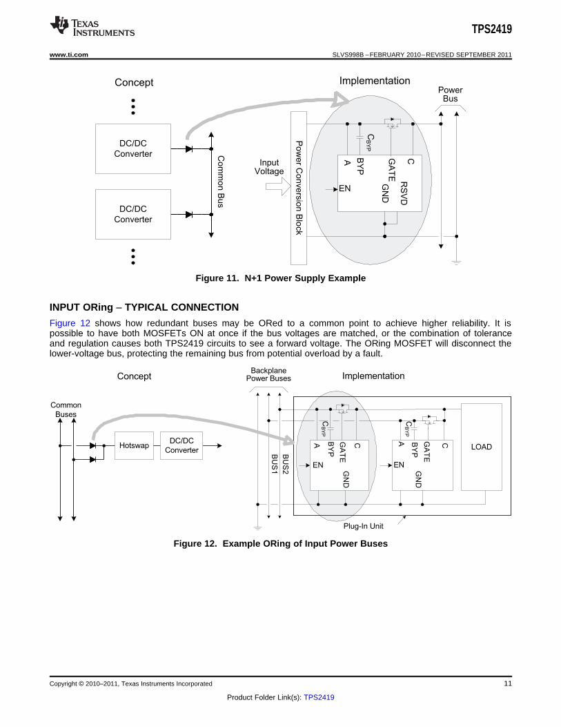
The strong gate (pulsed) pull-down current can turn the ORing MOSFET(s) off in the 100 - 200 ns time frame.While this serves to rapidly stop the reverse current buildup, it has a side effect of inducing a voltage transient onthe input bus, the output bus, and ground. One transient source is the GATE turn-off current itself, which excitesparasitic L-C tank circuits. A second transient source is the energy stored in power bus inductance driving avoltage surge and ringing as reverse MOSFET current is interrupted. Both of these effects can be reduced bylimiting the GATE discharge current with a series resistor in the 10 Ω to 200 Ω range. This both reduces the peakdischarge current, and slows the MOSFET turnoff, reducing the di/dt. A careful tradeoff of peak reverse currentand the effects of the voltage transient may be required.
An example of turnoff speed with and without GATE resistance is illustrated by the circuit of Figure 13. Figure 14and Figure 15 show GATE, the MOSFET gate, and VC-ac for similar turnoff transients and gate resistors of 0 Ωand 51 Ω. A substancial reduction in noise is shown for a difference of 90ns in actual current termination. Thesetechniques may be used in conjunction with clamping and snubbing techniques discussed in RECOMMENDEDOPERATING RANGE. Figure 13 also demonstrates the filtering discussed in the next section.
Figure 13. Circuit for Gate Resistor Waveforms
Copyright © 2010–2011, Texas Instruments Incorporated 13
Product Folder Link(s): TPS2419
Time 50ns/DIV
Turn onThreshold
Configuration: 2 x ( CSD16401,
TI with 0 gate resistors)WVC Output
MOSFETstops conducting
VGATE_2419
VGATE_MOSFET
10 V
/DIV
100 m
v/D
IVA
C_C
ou
ple
d10 V
/DIV
Time 50ns/DIV
Configuration: 2 x ( CSD16401,
TI with 51 in gate)WVC Output
MOSFETstops conducting
VGATE_2419
VGATE_MOSFET
10
V/D
IV
10
0 m
v/D
IVA
C_
Co
up
led
10
V/D
IV
TPS2419
SLVS998B –FEBRUARY 2010–REVISED SEPTEMBER 2011 www.ti.com
Figure 14. Gate Turnoff Waveforms with RGATE = 0Ω
Figure 15. Gate Turnoff Waveforms with RGATE = 51Ω
14 Copyright © 2010–2011, Texas Instruments Incorporated
Product Folder Link(s): TPS2419

0.47mF0.47mF
0.47mF
TO “C”
FROM “GATE”
Z = 600W,0.1W, 2A
TO “A”
CASE 1
0.47mF 0.47mF
0.47mF
TO “C”
FROM “GATE”
TO “A”
CASE 2
1W
TPS2419
www.ti.com SLVS998B –FEBRUARY 2010–REVISED SEPTEMBER 2011
Input Filtering
Voltage transients, converter switching noise and ripple, and ringing due to current interruptions can potentiallycause undesired on-off cycling, especially at very light loads. This includes voltage gradients (especially at MHzfrequencies) across the ground plane effecting the apparent V(A) and V(C). The effects of these unwanted signalscan be reduced by providing input filtering as shown in Figure 16 and Figure 13. There are two potentialproblems that the filter might have to help with, 1) internally generated switching noise, and 2) fast ringingtransients caused by nearby power system events. Case 2 (in Figure 16) filtering is better at suppressing internalswitching noise and Case 1 is better for large bus transients in the megahertz range. The "Z" element in CASE 1is a high-impedance ferrite bead with low resistance to limit the dc voltage error. The L-C filter limits the apparentV(A) voltage swings during high-speed transients. The L-C in series with A also causes a phase delay in sensedsteady-state switching noise, creating an apparent additional V(AC).
The filter capacitors should be located close to the TPS2419's GND pin and be connected to GND by a solidplane. The A-C capacitor should be located directly across the TPS2419 pins. These values were empiricallychosen in a particular test setup and may have to be tuned for different systems.
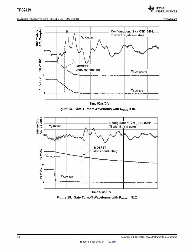
The waveform of Figure 17 shows turnon in the presence of 135 mVpp ripple by the circuit of Figure 13. TheORing circuit was loaded with 10 kΩ parallel to 0.1 µF, and had only a -4.5 mV turnoff threshold. This condition isoften difficult to turn on into due to the V(A-C) difference that occurs when the MOSFET diode peak charges theoutput. The output voltage was monitored with the oscilloscope probe ac-coupled, causing visual artifacts due tothe probe settling time. The increase in output ripple is evident as the dynamic impedance of the MOSFET diodeis shorted by the channel resistance.
Selection of the A and C sense points can also play a role in limiting unwanted turnoff events. Sensing voltagesat bus bypass capacitors may benefit operation by limiting the apparent switching and transient noise.
The TPS2419 uses C as both a voltage sense and power pin. Placing resistance in this lead will cause areduction in V(C) due to IxR voltage drop, changing the apparent turnon and turnoff thresholds.
Figure 16. Input Filtering Configurations
Copyright © 2010–2011, Texas Instruments Incorporated 15
Product Folder Link(s): TPS2419
Time 10 s/DIVm
V = 12 V,
Load = 10 k || 0.1 FC
W mVA-C
Note slight (-) offsetin differential probe
VGATE
V OutputC
135mVPP
10V
100 m
v/D
IVA
C_C
ou
ple
d200 m
V/D
IV
15V
TPS2419
SLVS998B –FEBRUARY 2010–REVISED SEPTEMBER 2011 www.ti.com
Figure 17. Turnon with Noisy Power Rail
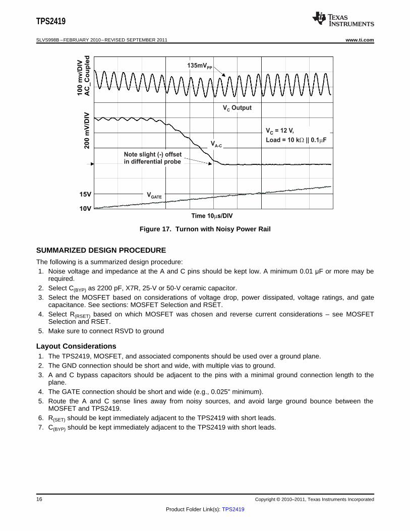
SUMMARIZED DESIGN PROCEDURE
The following is a summarized design procedure:1. Noise voltage and impedance at the A and C pins should be kept low. A minimum 0.01 μF or more may be
required.2. Select C(BYP) as 2200 pF, X7R, 25-V or 50-V ceramic capacitor.3. Select the MOSFET based on considerations of voltage drop, power dissipated, voltage ratings, and gate
capacitance. See sections: MOSFET Selection and RSET.4. Select R(RSET) based on which MOSFET was chosen and reverse current considerations – see MOSFET
Selection and RSET.5. Make sure to connect RSVD to ground
Layout Considerations1. The TPS2419, MOSFET, and associated components should be used over a ground plane.2. The GND connection should be short and wide, with multiple vias to ground.3. A and C bypass capacitors should be adjacent to the pins with a minimal ground connection length to the
plane.4. The GATE connection should be short and wide (e.g., 0.025" minimum).5. Route the A and C sense lines away from noisy sources, and avoid large ground bounce between the
MOSFET and TPS2419.6. R(SET) should be kept immediately adjacent to the TPS2419 with short leads.7. C(BYP) should be kept immediately adjacent to the TPS2419 with short leads.
16 Copyright © 2010–2011, Texas Instruments Incorporated
Product Folder Link(s): TPS2419
TPS2419
www.ti.com SLVS998B –FEBRUARY 2010–REVISED SEPTEMBER 2011
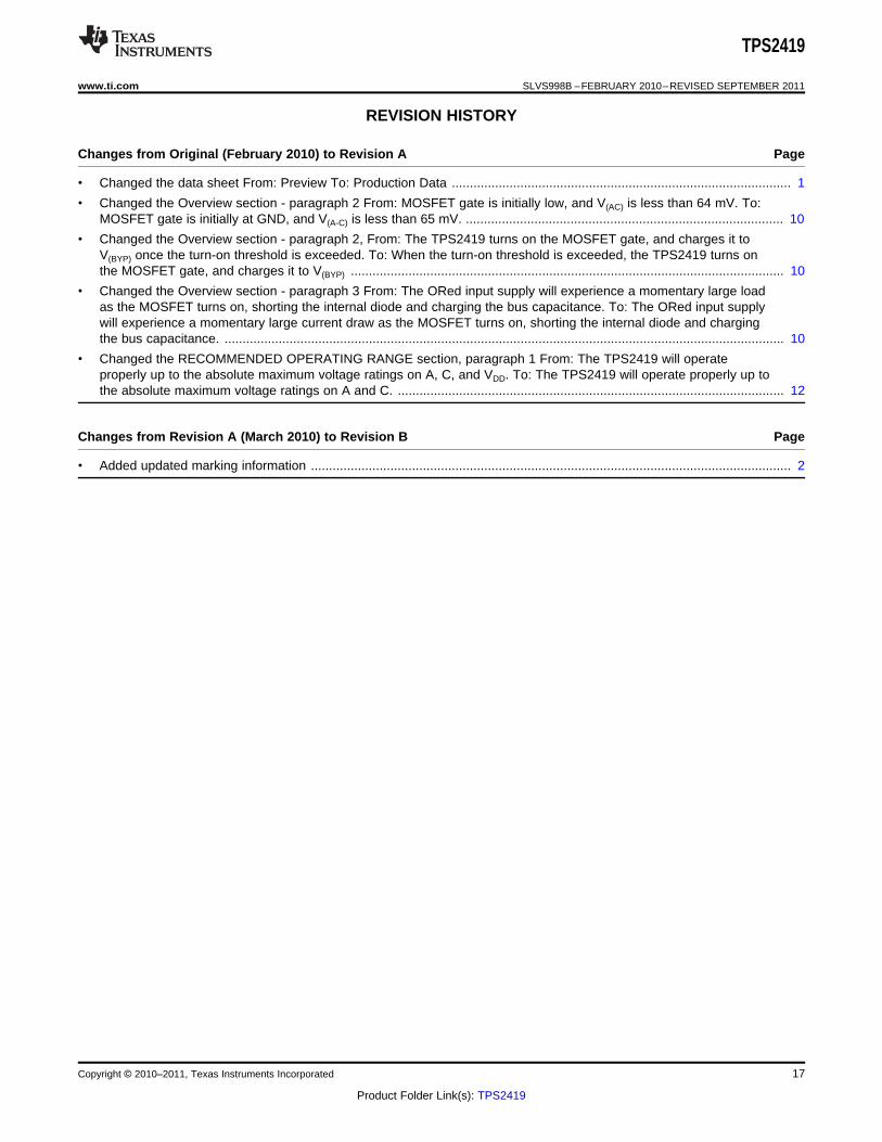
REVISION HISTORY
Changes from Original (February 2010) to Revision A Page
• Changed the data sheet From: Preview To: Production Data .............................................................................................. 1
• Changed the Overview section - paragraph 2 From: MOSFET gate is initially low, and V(AC) is less than 64 mV. To:MOSFET gate is initially at GND, and V(A-C) is less than 65 mV. ........................................................................................ 10
• Changed the Overview section - paragraph 2, From: The TPS2419 turns on the MOSFET gate, and charges it toV(BYP) once the turn-on threshold is exceeded. To: When the turn-on threshold is exceeded, the TPS2419 turns onthe MOSFET gate, and charges it to V(BYP) ........................................................................................................................ 10
• Changed the Overview section - paragraph 3 From: The ORed input supply will experience a momentary large loadas the MOSFET turns on, shorting the internal diode and charging the bus capacitance. To: The ORed input supplywill experience a momentary large current draw as the MOSFET turns on, shorting the internal diode and chargingthe bus capacitance. ........................................................................................................................................................... 10
• Changed the RECOMMENDED OPERATING RANGE section, paragraph 1 From: The TPS2419 will operateproperly up to the absolute maximum voltage ratings on A, C, and VDD. To: The TPS2419 will operate properly up tothe absolute maximum voltage ratings on A and C. ........................................................................................................... 12
Changes from Revision A (March 2010) to Revision B Page
• Added updated marking information ..................................................................................................................................... 2
Copyright © 2010–2011, Texas Instruments Incorporated 17
Product Folder Link(s): TPS2419
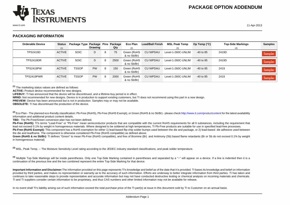
PACKAGE OPTION ADDENDUM
www.ti.com 11-Apr-2013
Addendum-Page 1
PACKAGING INFORMATION
Orderable Device Status(1)
Package Type PackageDrawing
Pins PackageQty
Eco Plan(2)
Lead/Ball Finish MSL Peak Temp(3)
Op Temp (°C) Top-Side Markings(4)
Samples
TPS2419D ACTIVE SOIC D 8 75 Green (RoHS& no Sb/Br)
CU NIPDAU Level-1-260C-UNLIM -40 to 85 2419D
TPS2419DR ACTIVE SOIC D 8 2500 Green (RoHS& no Sb/Br)
CU NIPDAU Level-1-260C-UNLIM -40 to 85 2419D
TPS2419PW ACTIVE TSSOP PW 8 150 Green (RoHS& no Sb/Br)
CU NIPDAU Level-1-260C-UNLIM -40 to 85 2419
TPS2419PWR ACTIVE TSSOP PW 8 2000 Green (RoHS& no Sb/Br)
CU NIPDAU Level-1-260C-UNLIM -40 to 85 2419
(1) The marketing status values are defined as follows:ACTIVE: Product device recommended for new designs.LIFEBUY: TI has announced that the device will be discontinued, and a lifetime-buy period is in effect.NRND: Not recommended for new designs. Device is in production to support existing customers, but TI does not recommend using this part in a new design.PREVIEW: Device has been announced but is not in production. Samples may or may not be available.OBSOLETE: TI has discontinued the production of the device.
(2) Eco Plan - The planned eco-friendly classification: Pb-Free (RoHS), Pb-Free (RoHS Exempt), or Green (RoHS & no Sb/Br) - please check http://www.ti.com/productcontent for the latest availabilityinformation and additional product content details.TBD: The Pb-Free/Green conversion plan has not been defined.Pb-Free (RoHS): TI's terms "Lead-Free" or "Pb-Free" mean semiconductor products that are compatible with the current RoHS requirements for all 6 substances, including the requirement thatlead not exceed 0.1% by weight in homogeneous materials. Where designed to be soldered at high temperatures, TI Pb-Free products are suitable for use in specified lead-free processes.Pb-Free (RoHS Exempt): This component has a RoHS exemption for either 1) lead-based flip-chip solder bumps used between the die and package, or 2) lead-based die adhesive used betweenthe die and leadframe. The component is otherwise considered Pb-Free (RoHS compatible) as defined above.Green (RoHS & no Sb/Br): TI defines "Green" to mean Pb-Free (RoHS compatible), and free of Bromine (Br) and Antimony (Sb) based flame retardants (Br or Sb do not exceed 0.1% by weightin homogeneous material)
(3) MSL, Peak Temp. -- The Moisture Sensitivity Level rating according to the JEDEC industry standard classifications, and peak solder temperature.
(4) Multiple Top-Side Markings will be inside parentheses. Only one Top-Side Marking contained in parentheses and separated by a "~" will appear on a device. If a line is indented then it is acontinuation of the previous line and the two combined represent the entire Top-Side Marking for that device.
Important Information and Disclaimer:The information provided on this page represents TI's knowledge and belief as of the date that it is provided. TI bases its knowledge and belief on informationprovided by third parties, and makes no representation or warranty as to the accuracy of such information. Efforts are underway to better integrate information from third parties. TI has taken andcontinues to take reasonable steps to provide representative and accurate information but may not have conducted destructive testing or chemical analysis on incoming materials and chemicals.TI and TI suppliers consider certain information to be proprietary, and thus CAS numbers and other limited information may not be available for release.
In no event shall TI's liability arising out of such information exceed the total purchase price of the TI part(s) at issue in this document sold by TI to Customer on an annual basis.
PACKAGE OPTION ADDENDUM
www.ti.com 11-Apr-2013
Addendum-Page 2
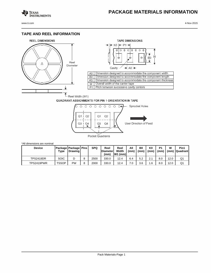
TAPE AND REEL INFORMATION
*All dimensions are nominal
Device PackageType
PackageDrawing
Pins SPQ ReelDiameter
(mm)
ReelWidth
W1 (mm)
A0(mm)
B0(mm)
K0(mm)
P1(mm)
W(mm)
Pin1Quadrant
TPS2419DR SOIC D 8 2500 330.0 12.4 6.4 5.2 2.1 8.0 12.0 Q1
TPS2419PWR TSSOP PW 8 2000 330.0 12.4 7.0 3.6 1.6 8.0 12.0 Q1
PACKAGE MATERIALS INFORMATION
www.ti.com 4-Nov-2015
Pack Materials-Page 1

*All dimensions are nominal
Device Package Type Package Drawing Pins SPQ Length (mm) Width (mm) Height (mm)
TPS2419DR SOIC D 8 2500 340.5 338.1 20.6
TPS2419PWR TSSOP PW 8 2000 367.0 367.0 35.0
PACKAGE MATERIALS INFORMATION
www.ti.com 4-Nov-2015
Pack Materials-Page 2
www.ti.com
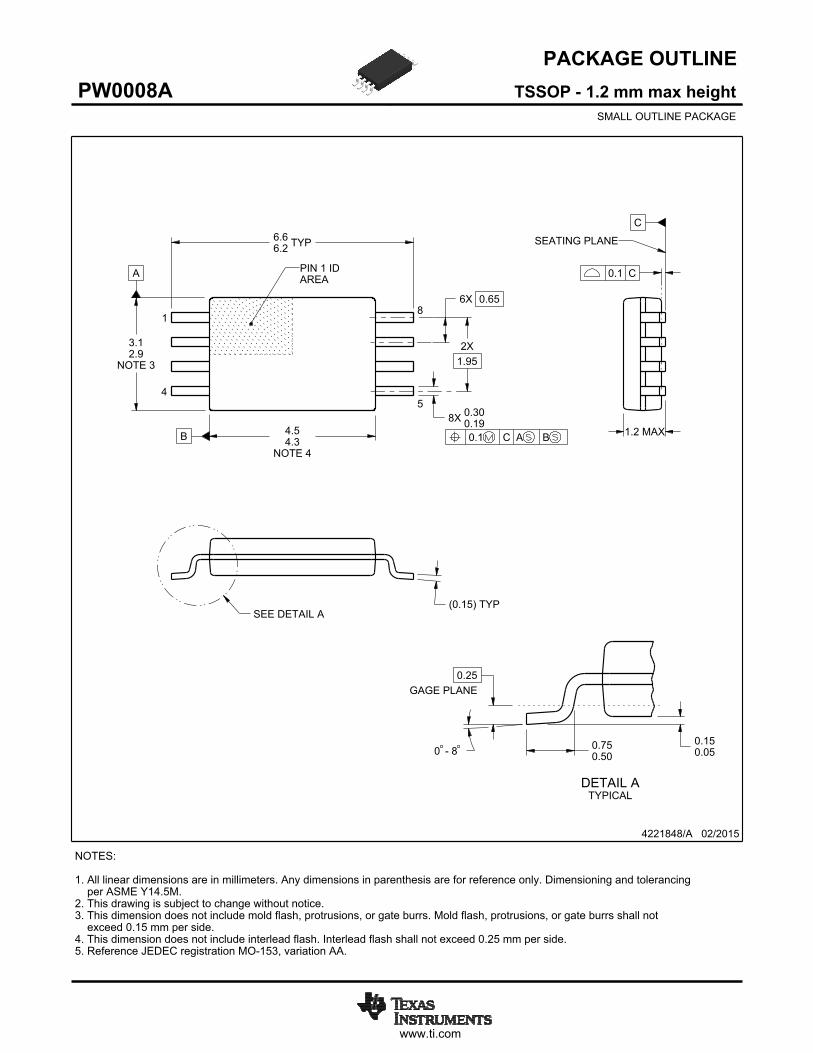
PACKAGE OUTLINE
C
TYP6.66.2
1.2 MAX
6X 0.65
8X 0.300.19
2X1.95
0.150.05
(0.15) TYP
0 - 8
0.25GAGE PLANE
0.750.50
A
NOTE 3
3.12.9
BNOTE 4
4.54.3
4221848/A 02/2015
TSSOP - 1.2 mm max heightPW0008ASMALL OUTLINE PACKAGE
NOTES: 1. All linear dimensions are in millimeters. Any dimensions in parenthesis are for reference only. Dimensioning and tolerancing per ASME Y14.5M. 2. This drawing is subject to change without notice. 3. This dimension does not include mold flash, protrusions, or gate burrs. Mold flash, protrusions, or gate burrs shall not exceed 0.15 mm per side. 4. This dimension does not include interlead flash. Interlead flash shall not exceed 0.25 mm per side.5. Reference JEDEC registration MO-153, variation AA.
18
0.1 C A B
54
PIN 1 IDAREA
SEATING PLANE
0.1 C
SEE DETAIL A
DETAIL ATYPICAL
SCALE 2.800

www.ti.com
EXAMPLE BOARD LAYOUT
(5.8)
0.05 MAXALL AROUND
0.05 MINALL AROUND
8X (1.5)8X (0.45)
6X (0.65)
(R )TYP
0.05
4221848/A 02/2015
TSSOP - 1.2 mm max heightPW0008ASMALL OUTLINE PACKAGE
SYMM
SYMM
LAND PATTERN EXAMPLESCALE:10X
1
45
8
NOTES: (continued) 6. Publication IPC-7351 may have alternate designs. 7. Solder mask tolerances between and around signal pads can vary based on board fabrication site.
METALSOLDER MASKOPENING
NON SOLDER MASKDEFINED
SOLDER MASK DETAILSNOT TO SCALE
SOLDER MASKOPENING
METAL UNDERSOLDER MASK
SOLDER MASKDEFINED

www.ti.com
EXAMPLE STENCIL DESIGN
(5.8)
6X (0.65)
8X (0.45)8X (1.5)
(R ) TYP0.05
4221848/A 02/2015
TSSOP - 1.2 mm max heightPW0008ASMALL OUTLINE PACKAGE
NOTES: (continued) 8. Laser cutting apertures with trapezoidal walls and rounded corners may offer better paste release. IPC-7525 may have alternate design recommendations. 9. Board assembly site may have different recommendations for stencil design.
SYMM
SYMM
1
45
8
SOLDER PASTE EXAMPLEBASED ON 0.125 mm THICK STENCIL
SCALE:10X


IMPORTANT NOTICE
Texas Instruments Incorporated and its subsidiaries (TI) reserve the right to make corrections, enhancements, improvements and otherchanges to its semiconductor products and services per JESD46, latest issue, and to discontinue any product or service per JESD48, latestissue. Buyers should obtain the latest relevant information before placing orders and should verify that such information is current andcomplete. All semiconductor products (also referred to herein as “components”) are sold subject to TI’s terms and conditions of salesupplied at the time of order acknowledgment.TI warrants performance of its components to the specifications applicable at the time of sale, in accordance with the warranty in TI’s termsand conditions of sale of semiconductor products. Testing and other quality control techniques are used to the extent TI deems necessaryto support this warranty. Except where mandated by applicable law, testing of all parameters of each component is not necessarilyperformed.TI assumes no liability for applications assistance or the design of Buyers’ products. Buyers are responsible for their products andapplications using TI components. To minimize the risks associated with Buyers’ products and applications, Buyers should provideadequate design and operating safeguards.TI does not warrant or represent that any license, either express or implied, is granted under any patent right, copyright, mask work right, orother intellectual property right relating to any combination, machine, or process in which TI components or services are used. Informationpublished by TI regarding third-party products or services does not constitute a license to use such products or services or a warranty orendorsement thereof. Use of such information may require a license from a third party under the patents or other intellectual property of thethird party, or a license from TI under the patents or other intellectual property of TI.Reproduction of significant portions of TI information in TI data books or data sheets is permissible only if reproduction is without alterationand is accompanied by all associated warranties, conditions, limitations, and notices. TI is not responsible or liable for such altereddocumentation. Information of third parties may be subject to additional restrictions.Resale of TI components or services with statements different from or beyond the parameters stated by TI for that component or servicevoids all express and any implied warranties for the associated TI component or service and is an unfair and deceptive business practice.TI is not responsible or liable for any such statements.Buyer acknowledges and agrees that it is solely responsible for compliance with all legal, regulatory and safety-related requirementsconcerning its products, and any use of TI components in its applications, notwithstanding any applications-related information or supportthat may be provided by TI. Buyer represents and agrees that it has all the necessary expertise to create and implement safeguards whichanticipate dangerous consequences of failures, monitor failures and their consequences, lessen the likelihood of failures that might causeharm and take appropriate remedial actions. Buyer will fully indemnify TI and its representatives against any damages arising out of the useof any TI components in safety-critical applications.In some cases, TI components may be promoted specifically to facilitate safety-related applications. With such components, TI’s goal is tohelp enable customers to design and create their own end-product solutions that meet applicable functional safety standards andrequirements. Nonetheless, such components are subject to these terms.No TI components are authorized for use in FDA Class III (or similar life-critical medical equipment) unless authorized officers of the partieshave executed a special agreement specifically governing such use.Only those TI components which TI has specifically designated as military grade or “enhanced plastic” are designed and intended for use inmilitary/aerospace applications or environments. Buyer acknowledges and agrees that any military or aerospace use of TI componentswhich have not been so designated is solely at the Buyer's risk, and that Buyer is solely responsible for compliance with all legal andregulatory requirements in connection with such use.TI has specifically designated certain components as meeting ISO/TS16949 requirements, mainly for automotive use. In any case of use ofnon-designated products, TI will not be responsible for any failure to meet ISO/TS16949.
Products ApplicationsAudio www.ti.com/audio Automotive and Transportation www.ti.com/automotiveAmplifiers amplifier.ti.com Communications and Telecom www.ti.com/communicationsData Converters dataconverter.ti.com Computers and Peripherals www.ti.com/computersDLP® Products www.dlp.com Consumer Electronics www.ti.com/consumer-appsDSP dsp.ti.com Energy and Lighting www.ti.com/energyClocks and Timers www.ti.com/clocks Industrial www.ti.com/industrialInterface interface.ti.com Medical www.ti.com/medicalLogic logic.ti.com Security www.ti.com/securityPower Mgmt power.ti.com Space, Avionics and Defense www.ti.com/space-avionics-defenseMicrocontrollers microcontroller.ti.com Video and Imaging www.ti.com/videoRFID www.ti-rfid.comOMAP Applications Processors www.ti.com/omap TI E2E Community e2e.ti.comWireless Connectivity www.ti.com/wirelessconnectivity
Mailing Address: Texas Instruments, Post Office Box 655303, Dallas, Texas 75265Copyright © 2015, Texas Instruments Incorporated