
Multiscale Modeling and Control of RF Diode Sputter ... · Multiscale Modeling and Control of RF...
12
Multiscale Modeling and Control of RF Diode Sputter Deposition for GMR Thin Films S. Ghosal, R. L. Kosut, J. L. Ebert, and L. L. Porter II Abstract − Radio frequency (RF) diode sputtering is widely used for depositing Giant Magneto-Resistive (GMR) thin films for multilayers, spin valves, and spin-dependent tunneling (SDT) devices used in data storage, computer memory, etc. However, the thin films thus produced often show unacceptably high variation in GMR properties from wafer to wafer. This paper describes a modeling and control effort that was undertaken for improving run-to-run repeatability. A multiscale input-output model was developed for the primary physical phenomena in the deposition process − gas flow, plasma discharge, sputtering, and atom transport. The model predicts the deposition rate, the energy distribution of sputtered atoms, and their sensitivity to deposition conditions such as power, working gas type, pressure, gas temperature, and electrode spacing. Simulations with this model were used to determine the process parameters to which the wafer properties have the maximum sensitivity. Experiments were performed to determine the relative importance of these parameters. Based on the results, a controller was designed to regulate the time-integrated target bias voltage. Implementation of the controller reduced wafer-to-wafer variation of GMR properties by over 50%. Additionally, application of control to SDT wafers led to improvement and optimization of the process. I. INTRODUCTION Giant Magneto-Resistive (GMR) multilayer wafer processing consists of depositing a stack of as many as sixteen ultra-thin layers of metals in a specific order, including three conducting layers of copper-silver-gold (CuAgAu, 16.5 Å), six layers of ferromagnetic cobalt-iron (CoFe, 15 Å), four layers of nickel-cobalt-iron (NiCoFe, 20 Å and 40 Å). GMR devices exhibit large (“giant”) changes in electrical resistance with small changes in applied magnetic fields [1]. They find increasing use in sensors, hard disk drive read heads, and Magnetic Random Access Memory (MRAM) [1], [2]. However, sputter-deposited GMR films often show great variability of GMR properties wafer-to-wafer even within a single lot. One common method for depositing GMR thin films is RF diode sputtering where a plasma is used to ionize gas This work was supported by the Applied Computation and Mathematics Program at Defence Advanced Research Projects Agency (DARPA). Dr. A. Tsao was the program manager. The authors are with SC Solutions, Inc., Sunnyvale, CA 94085. Corresponding author: S. Ghosal, phone: 408 617 4520, fax: 408 617 4521, e-mail: [email protected]. atoms in the processing chamber which are then driven to the target by an electric field. These high energy atoms knock out, or sputter, neutral atoms from the target, many of which then drift to the wafer below after multiple collisions with the gas atoms. The development and computational implementation of physical models for RF diode sputtering, which have been calibrated and refined using appropriate experimental results, can reduce the time consuming and costly trial-and- error approach used to design, operate, and control deposition systems used for the reliable fabrication of high- quality thin films. To meet these objectives, a multiscale model of sputter deposition of thin metal films was developed that includes the primary physical phenomena − gas flow within the sputter chamber, plasma discharge, sputtering from the target, and transport of the sputtered atom to the wafer surface. The resulting multiscale input- output model is capable of predicting the thin-film deposition rate, the energy and direction distribution of the sputtered metal atoms, both upon emission at the target and just prior to deposition at the substrate, and their sensitivity to deposition conditions such as power, working gas type, pressure, gas temperature, and electrode spacing. Target Target Target Target Tray Tray Poppet value Tray cut-away Chamber inner wall Dark shield Susceptor electrode Substrate Counter weight Exhaust V rf RF-power Figure 1: Schematic of the RF diode sputter chamber. A. The RF Diode Deposition Process A schematic diagram of an RF diode sputter chamber is shown in Figure 1. The chamber depicted in this figure
Transcript of Multiscale Modeling and Control of RF Diode Sputter ... · Multiscale Modeling and Control of RF...
Multiscale Modeling and Control of RF Diode Sputter Deposition for GMR Thin Films
S. Ghosal, R. L. Kosut, J. L. Ebert, and L. L. Porter II
Abstract − Radio frequency (RF) diode sputtering is widely used for depositing Giant Magneto-Resistive (GMR) thin films for multilayers, spin valves, and spin-dependent tunneling (SDT) devices used in data storage, computer memory, etc. However, the thin films thus produced often show unacceptably high variation in GMR properties from wafer to wafer. This paper describes a modeling and control effort that was undertaken for improving run-to-run repeatability. A multiscale input-output model was developed for the primary physical phenomena in the deposition process − gas flow, plasma discharge, sputtering, and atom transport. The model predicts the deposition rate, the energy distribution of sputtered atoms, and their sensitivity to deposition conditions such as power, working gas type, pressure, gas temperature, and electrode spacing. Simulations with this model were used to determine the process parameters to which the wafer properties have the maximum sensitivity. Experiments were performed to determine the relative importance of these parameters. Based on the results, a controller was designed to regulate the time-integrated target bias voltage. Implementation of the controller reduced wafer-to-wafer variation of GMR properties by over 50%. Additionally, application of control to SDT wafers led to improvement and optimization of the process.
I. INTRODUCTION Giant Magneto-Resistive (GMR) multilayer wafer processing consists of depositing a stack of as many as sixteen ultra-thin layers of metals in a specific order, including three conducting layers of copper-silver-gold (CuAgAu, 16.5 Å), six layers of ferromagnetic cobalt-iron (CoFe, 15 Å), four layers of nickel-cobalt-iron (NiCoFe, 20 Å and 40 Å). GMR devices exhibit large (“giant”) changes in electrical resistance with small changes in applied magnetic fields [1]. They find increasing use in sensors, hard disk drive read heads, and Magnetic Random Access Memory (MRAM) [1], [2]. However, sputter-deposited GMR films often show great variability of GMR properties wafer-to-wafer even within a single lot.
One common method for depositing GMR thin films is RF diode sputtering where a plasma is used to ionize gas
This work was supported by the Applied Computation and Mathematics Program at Defence Advanced Research Projects Agency (DARPA). Dr. A. Tsao was the program manager. The authors are with SC Solutions, Inc., Sunnyvale, CA 94085. Corresponding author: S. Ghosal, phone: 408 617 4520, fax: 408 617 4521, e-mail: [email protected].
atoms in the processing chamber which are then driven to the target by an electric field. These high energy atoms knock out, or sputter, neutral atoms from the target, many of which then drift to the wafer below after multiple collisions with the gas atoms.
The development and computational implementation of physical models for RF diode sputtering, which have been calibrated and refined using appropriate experimental results, can reduce the time consuming and costly trial-and-error approach used to design, operate, and control deposition systems used for the reliable fabrication of high-quality thin films. To meet these objectives, a multiscale model of sputter deposition of thin metal films was developed that includes the primary physical phenomena − gas flow within the sputter chamber, plasma discharge, sputtering from the target, and transport of the sputtered atom to the wafer surface. The resulting multiscale input-output model is capable of predicting the thin-film deposition rate, the energy and direction distribution of the sputtered metal atoms, both upon emission at the target and just prior to deposition at the substrate, and their sensitivity to deposition conditions such as power, working gas type, pressure, gas temperature, and electrode spacing.
Target
Target
Target
Target
Tray
TrayPoppetvalue
Tray cut-away
Chamber inner wall
Dark shield
Susceptor electrode
Substrate Counter weight
Exhaust
Vrf
RF-power
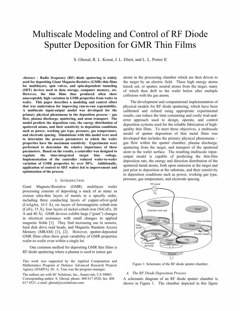
Figure 1: Schematic of the RF diode sputter chamber.
A. The RF Diode Deposition Process A schematic diagram of an RF diode sputter chamber is shown in Figure 1. The chamber depicted in this figure
represents the essential elements of a Perkins Elmer 2400 sputtering system. Copper was chosen for this study because it is commonly used as the conducting layer in several giant magnetoresistive applications [1], [2]. The copper target for sputtering was mounted at the top of the chamber while the wafer on which the thin film is deposited is mounted at the bottom of the chamber. Although four targets are present in the chamber during processing, only the target directly above the substrate is active during the deposition of a layer. Argon gas at low pressure (20−50 mTorr) flows continuously through the chamber. An RF plasma discharge is generated and maintained between the target electrode and the wafer (substrate) electrode by means of a power supply and RF matching network. Argon ions formed in the plasma bombard the copper target and result in copper atom ejection, which propagate through the argon and are deposited on the wafer substrate.
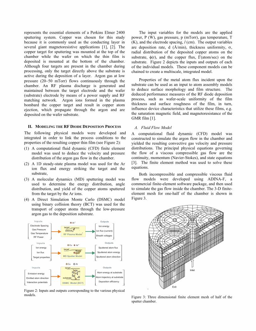
II. MODELING THE RF DIODE DEPOSITION PROCESS The following physical models were developed and integrated in order to link the process conditions to the properties of the resulting copper thin film (see Figure 2): (1) A computational fluid dynamic (CFD) finite element
model was used to deduce the velocity and pressure distribution of the argon gas flow in the chamber.
(2) A 1D steady-state plasma model was used for the Ar ion flux and energy striking the target and the substrate,
(3) A molecular dynamics (MD) sputtering model was used to determine the energy distribution, angle distribution, and yield of the copper atoms sputtered from the target by the Ar ions.
(4) A Direct Simulation Monte Carlo (DSMC) model using binary collision theory (BCT) was used for the transport of copper atoms through the low-pressure argon gas to the deposition substrate.
Ar+
plasmatarget
RF Plasma Model1
Outputs
Ion energy
Sheath voltages
Ion flux (current)Gas Pressure
Gas Temperature
RF Power
Electrode Spacing
I nputs
targetgas
substrate
DSMC Model (BCT)
OutputsInputs
Atom energy at substrate
Interaction potentials
Emission energy
Emitted atom direction Atom trajectory at substrate
Deposition efficiency
Cu Ar
target
MD Sputter Model
Outputs
Sputtered atom energyIon flux
I nputs
Ion energy
Sputtered atom direction
Sputtered atom flux
Target properties
Ar+Cu
Figure 2: Inputs and outputs corresponding to the various physical models.
The input variables for the models are the applied power, P (W), gas pressure, p (mTorr), gas temperature, T (K), and the electrode spacing, l (cm). The output variables are deposition rate, d (Å/min), thickness uniformity, σ, radial distribution of the deposited copper atoms on the substrate, φ(r), and the copper flux, Γ(atom/sec) on the substrate. Figure 2 depicts the inputs and outputs of each of the individual models. These component models can be chained to create a multiscale, integrated model.
Properties of the metal atom flux incident upon the substrate can be used as an input to atom assembly models to deduce surface morphology and film structure. The deduced performance measures of the RF diode deposition process, such as wafer-scale uniformity of the film thickness and surface roughness of the film, in turn, influence device characteristics that utilize these films, e.g. the saturation magnetic field, and magnetoresistance of the GMR film [1].
A. Fluid Flow Model A computational fluid dynamic (CFD) model was constructed to simulate the argon flow in the chamber and yielded the resulting convective gas velocity and pressure distributions. The principal physical equations governing the flow of a viscous compressible gas flow are the continuity, momentum (Navier-Stokes), and state equations [3]. The finite element method was used to solve these equations.
Both incompressible and compressible viscous fluid flow models were developed using ADINA-F, a commercial finite-element software package, and then used to simulate the gas flow inside the chamber. The 3-D finite-element mesh for one-half of the chamber is shown in Figure 3.
. Exit
Inlet
#1#2
#3
Figure 3: Three dimensional finite element mesh of half of the sputter chamber.
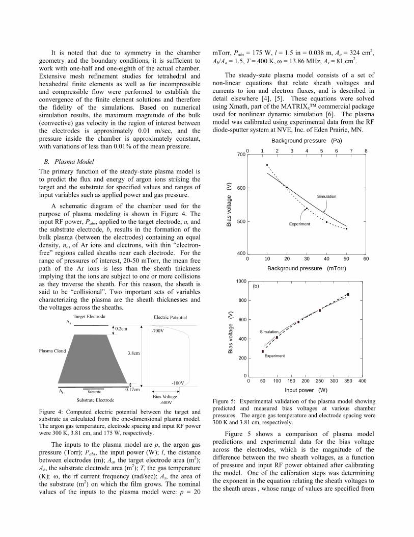
It is noted that due to symmetry in the chamber geometry and the boundary conditions, it is sufficient to work with one-half and one-eighth of the actual chamber. Extensive mesh refinement studies for tetrahedral and hexahedral finite elements as well as for incompressible and compressible flow were performed to establish the convergence of the finite element solutions and therefore the fidelity of the simulations. Based on numerical simulation results, the maximum magnitude of the bulk (convective) gas velocity in the region of interest between the electrodes is approximately 0.01 m/sec, and the pressure inside the chamber is approximately constant, with variations of less than 0.01% of the mean pressure.
B. Plasma Model The primary function of the steady-state plasma model is to predict the flux and energy of argon ions striking the target and the substrate for specified values and ranges of input variables such as applied power and gas pressure.
A schematic diagram of the chamber used for the purpose of plasma modeling is shown in Figure 4. The input RF power, Pabs, applied to the target electrode, a, and the substrate electrode, b, results in the formation of the bulk plasma (between the electrodes) containing an equal density, no, of Ar ions and electrons, with thin “electron-free” regions called sheaths near each electrode. For the range of pressures of interest, 20-50 mTorr, the mean free path of the Ar ions is less than the sheath thickness implying that the ions are subject to one or more collisions as they traverse the sheath. For this reason, the sheath is said to be “collisional”. Two important sets of variables characterizing the plasma are the sheath thicknesses and the voltages across the sheaths.
Figure 4: Computed electric potential between the target and substrate as calculated from the one-dimensional plasma model. The argon gas temperature, electrode spacing and input RF power were 300 K, 3.81 cm, and 175 W, respectively.
The inputs to the plasma model are p, the argon gas pressure (Torr); Pabs, the input power (W); l, the distance between electrodes (m); Aa, the target electrode area (m2); Ab, the substrate electrode area (m2); T, the gas temperature (K); ω, the rf current frequency (rad/sec); As, the area of the substrate (m2) on which the film grows. The nominal values of the inputs to the plasma model were: p = 20
mTorr, Pabs = 175 W, l = 1.5 in = 0.038 m, Aa = 324 cm2, Ab/Aa = 1.5, T = 400 K, ω = 13.86 MHz, As = 81 cm2.
The steady-state plasma model consists of a set of non-linear equations that relate sheath voltages and currents to ion and electron fluxes, and is described in detail elsewhere [4], [5]. These equations were solved using Xmath, part of the MATRIXx™ commercial package used for nonlinear dynamic simulation [6]. The plasma model was calibrated using experimental data from the RF diode-sputter system at NVE, Inc. of Eden Prairie, MN.
Background pressure (mTorr)
Background pressure (Pa)
0 10 3020 40 50 60
0 1 2 3 4 5 6 7 8
400
500
600
700
Bia
s vo
ltage
(V
)
Simulation
Experiment
Input power (W)
0 50 150100 200 250 300 350 4000
200
400
600
800
1000
Bias
vol
tage
(V
)
(b)
Experiment
Simulation
Figure 5: Experimental validation of the plasma model showing predicted and measured bias voltages at various chamber pressures. The argon gas temperature and electrode spacing were 300 K and 3.81 cm, respectively.
Figure 5 shows a comparison of plasma model predictions and experimental data for the bias voltage across the electrodes, which is the magnitude of the difference between the two sheath voltages, as a function of pressure and input RF power obtained after calibrating the model. One of the calibration steps was determining the exponent in the equation relating the sheath voltages to the sheath areas , whose range of values are specified from
theory [5]. Other model simulation results showed that increasing the input power significantly increases the ion current density (or ion flux) and ion energy. Additionally, it was seen that increasing the pressure slightly increases the ion current density (or ion flux) while significantly decreasing the ion energy. Several other useful plasma model simulation results are documented in [5].
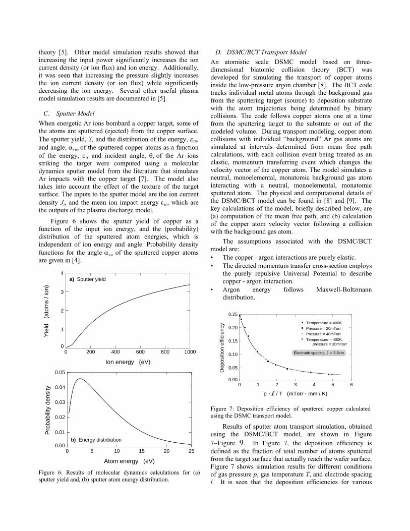
C. Sputter Model When energetic Ar ions bombard a copper target, some of the atoms are sputtered (ejected) from the copper surface. The sputter yield, Y, and the distribution of the energy, εcu, and angle, αcu, of the sputtered copper atoms as a function of the energy, εi, and incident angle, θ, of the Ar ions striking the target were computed using a molecular dynamics sputter model from the literature that simulates Ar impacts with the copper target [7]. The model also takes into account the effect of the texture of the target surface. The inputs to the sputter model are the ion current density Ji, and the mean ion impact energy εic, which are the outputs of the plasma discharge model.
Figure 6 shows the sputter yield of copper as a function of the input ion energy, and the (probability) distribution of the sputtered atom energies, which is independent of ion energy and angle. Probability density functions for the angle αcu of the sputtered copper atoms are given in [4].
Atom energy (eV)
0
b) Energy distribution0.00
0.01
0.02
0.03
0.04
0.05
Pro
babi
lity
dens
ity
5 1510 20 25
Ion energy (eV)
0
a) Sputter yield
0
1
2
3
4
Yie
ld
(ato
ms
/ ion
)
200 600400 800 1000
Figure 6: Results of molecular dynamics calculations for (a) sputter yield and, (b) sputter atom energy distribution.
D. DSMC/BCT Transport Model An atomistic scale DSMC model based on three-dimensional biatomic collision theory (BCT) was developed for simulating the transport of copper atoms inside the low-pressure argon chamber [8]. The BCT code tracks individual metal atoms through the background gas from the sputtering target (source) to deposition substrate with the atom trajectories being determined by binary collisions. The code follows copper atoms one at a time from the sputtering target to the substrate or out of the modeled volume. During transport modeling, copper atom collisions with individual “background” Ar gas atoms are simulated at intervals determined from mean free path calculations, with each collision event being treated as an elastic, momentum transferring event which changes the velocity vector of the copper atom. The model simulates a neutral, monoelemental, monatomic background gas atom interacting with a neutral, monoelemental, monatomic sputtered atom. The physical and computational details of the DSMC/BCT model can be found in [8] and [9]. The key calculations of the model, briefly described below, are (a) computation of the mean free path, and (b) calculation of the copper atom velocity vector following a collision with the background gas atom.
The assumptions associated with the DSMC/BCT model are: • The copper - argon interactions are purely elastic. • The directed momentum transfer cross-section employs
the purely repulsive Universal Potential to describe copper - argon interaction.
• Argon energy follows Maxwell-Boltzmann distribution.
p . / T (mTorr . mm / K)
0 1 32 4 5 60.00
0.05
0.10
0.15
0.20
0.25
Dep
ositi
on e
ffici
ency
Temperature = 400KPressure = 20mTorrPressure = 40mTorrTemperature = 400K, pressure = 20mTorr
Electrode spacing = 3.8cm
Figure 7: Deposition efficiency of sputtered copper calculated using the DSMC transport model.
Results of sputter atom transport simulation, obtained using the DSMC/BCT model, are shown in Figure 7−Figure 9. In Figure 7, the deposition efficiency is defined as the fraction of total number of atoms sputtered from the target surface that actually reach the wafer surface. Figure 7 shows simulation results for different conditions of gas pressure p, gas temperature T, and electrode spacing l. It is seen that the deposition efficiencies for various
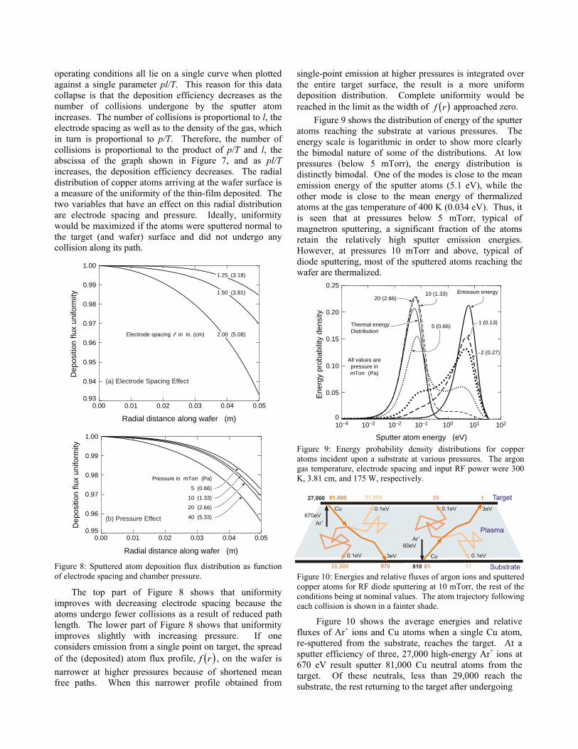
operating conditions all lie on a single curve when plotted against a single parameter pl/T. This reason for this data collapse is that the deposition efficiency decreases as the number of collisions undergone by the sputter atom increases. The number of collisions is proportional to l, the electrode spacing as well as to the density of the gas, which in turn is proportional to p/T. Therefore, the number of collisions is proportional to the product of p/T and l, the abscissa of the graph shown in Figure 7, and as pl/T increases, the deposition efficiency decreases. The radial distribution of copper atoms arriving at the wafer surface is a measure of the uniformity of the thin-film deposited. The two variables that have an effect on this radial distribution are electrode spacing and pressure. Ideally, uniformity would be maximized if the atoms were sputtered normal to the target (and wafer) surface and did not undergo any collision along its path.
Radial distance along wafer (m)
0.000.95
0.96
0.97
0.98
0.99
5 (0.66)
Pressure in mTorr (Pa)
10 (1.33)
20 (2.66)
40 (5.33)
1.00
Dep
ositi
on fl
ux u
nifo
rmity
0.01 0.030.02 0.04 0.05
Radial distance along wafer (m)
0.000.93
0.96
0.97
0.98
0.94
0.95
0.99
1.00
Dep
ositi
on fl
ux u
nifo
rmity
0.01 0.030.02 0.04 0.05
Electrode spacing in in. (cm)
1.25 (3.18)
1.50 (3.81)
2.00 (5.08)
(a) Electrode Spacing Effect
(b) Pressure Effect
Figure 8: Sputtered atom deposition flux distribution as function of electrode spacing and chamber pressure.
The top part of Figure 8 shows that uniformity improves with decreasing electrode spacing because the atoms undergo fewer collisions as a result of reduced path length. The lower part of Figure 8 shows that uniformity improves slightly with increasing pressure. If one considers emission from a single point on target, the spread of the (deposited) atom flux profile, ( )rf , on the wafer is narrower at higher pressures because of shortened mean free paths. When this narrower profile obtained from
single-point emission at higher pressures is integrated over the entire target surface, the result is a more uniform deposition distribution. Complete uniformity would be reached in the limit as the width of ( )rf approached zero.
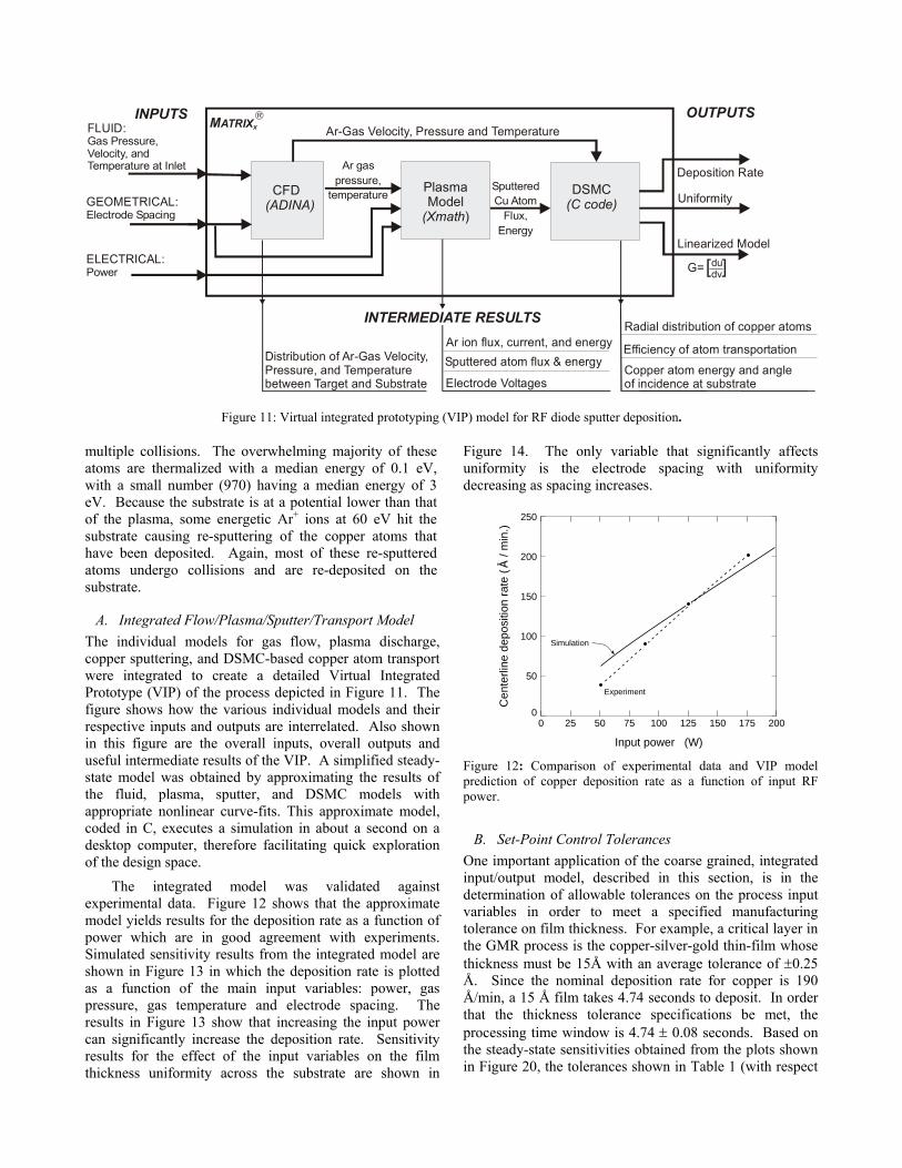
Figure 9 shows the distribution of energy of the sputter atoms reaching the substrate at various pressures. The energy scale is logarithmic in order to show more clearly the bimodal nature of some of the distributions. At low pressures (below 5 mTorr), the energy distribution is distinctly bimodal. One of the modes is close to the mean emission energy of the sputter atoms (5.1 eV), while the other mode is close to the mean energy of thermalized atoms at the gas temperature of 400 K (0.034 eV). Thus, it is seen that at pressures below 5 mTorr, typical of magnetron sputtering, a significant fraction of the atoms retain the relatively high sputter emission energies. However, at pressures 10 mTorr and above, typical of diode sputtering, most of the sputtered atoms reaching the wafer are thermalized.
Sputter atom energy (eV)
Emission energy
1 (0.13)
2 (0.27)
5 (0.66)
10 (1.33)20 (2.66)
Thermal energyDistribution
All values arepressure inmTorr (Pa)
0
0.05
0.10
0.15
0.20
0.25
Ene
rgy
prob
abili
ty d
ensi
ty
10–4 10–3 10–2 10–1 100 101 102
Figure 9: Energy probability density distributions for copper atoms incident upon a substrate at various pressures. The argon gas temperature, electrode spacing and input RF power were 300 K, 3.81 cm, and 175 W, respectively.
Ar+
Cu
Cu0.1eV 3eV
0.1eV
Ar+
0.1eV 3eV
0.1eV
Target
Substrate
670eV
60eV
Plasma
51810 8128,000 970
27,000 81,000 51,000 29 1
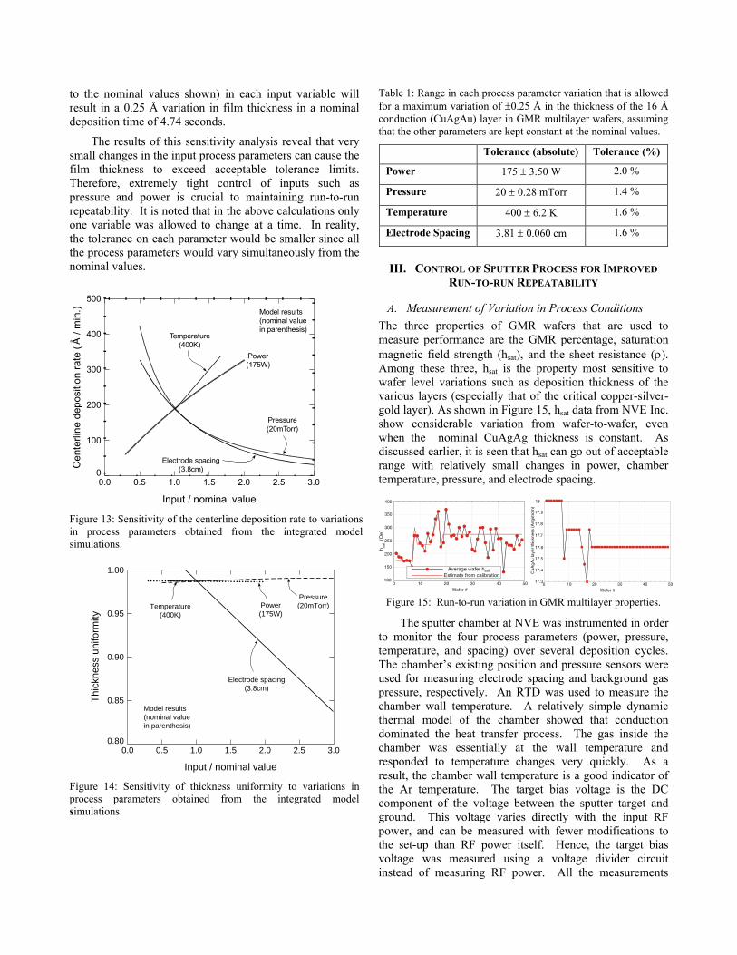
Figure 10: Energies and relative fluxes of argon ions and sputtered copper atoms for RF diode sputtering at 10 mTorr, the rest of the conditions being at nominal values. The atom trajectory following each collision is shown in a fainter shade.
Figure 10 shows the average energies and relative fluxes of Ar+ ions and Cu atoms when a single Cu atom, re-sputtered from the substrate, reaches the target. At a sputter efficiency of three, 27,000 high-energy Ar+ ions at 670 eV result sputter 81,000 Cu neutral atoms from the target. Of these neutrals, less than 29,000 reach the substrate, the rest returning to the target after undergoing
PlasmaModel
(Xmath)
CFD(ADINA)
DSMC(C code)
INTERMEDIATE RESULTS
FLUID:Gas Pressure,Velocity, and Temperature at Inlet
GEOMETRICAL:SpacingElectrode
ELECTRICAL:Power
Ar-Gas Velocity, Pressure and Temperature
Distribution of Ar-Gas Velocity, Pressure, and Temperaturebetween Target and Substrate
Ar ion flux, current, and energySputtered atom flux & energy
Electrode Voltages
Linearized Model
Radial distribution of copper atoms
Ar gaspressure,
temperatureSputteredCu Atom
Flux,Energy
Efficiency of atom transportationCopper atom energy and angleof incidence at substrate
Uniformity
Deposition Rate
G= dudv
INPUTS OUTPUTSMATRIXX
®
Figure 11: Virtual integrated prototyping (VIP) model for RF diode sputter deposition.
multiple collisions. The overwhelming majority of these atoms are thermalized with a median energy of 0.1 eV, with a small number (970) having a median energy of 3 eV. Because the substrate is at a potential lower than that of the plasma, some energetic Ar+ ions at 60 eV hit the substrate causing re-sputtering of the copper atoms that have been deposited. Again, most of these re-sputtered atoms undergo collisions and are re-deposited on the substrate.
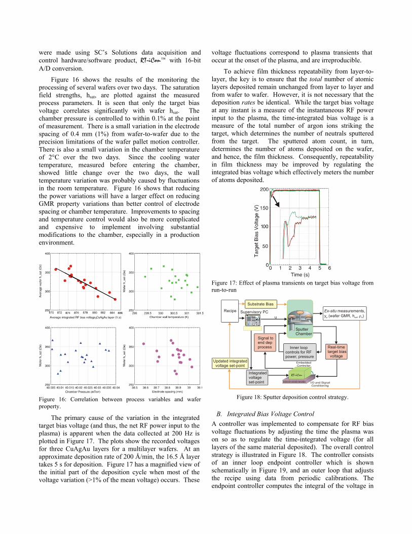
A. Integrated Flow/Plasma/Sputter/Transport Model The individual models for gas flow, plasma discharge, copper sputtering, and DSMC-based copper atom transport were integrated to create a detailed Virtual Integrated Prototype (VIP) of the process depicted in Figure 11. The figure shows how the various individual models and their respective inputs and outputs are interrelated. Also shown in this figure are the overall inputs, overall outputs and useful intermediate results of the VIP. A simplified steady-state model was obtained by approximating the results of the fluid, plasma, sputter, and DSMC models with appropriate nonlinear curve-fits. This approximate model, coded in C, executes a simulation in about a second on a desktop computer, therefore facilitating quick exploration of the design space.
The integrated model was validated against experimental data. Figure 12 shows that the approximate model yields results for the deposition rate as a function of power which are in good agreement with experiments. Simulated sensitivity results from the integrated model are shown in Figure 13 in which the deposition rate is plotted as a function of the main input variables: power, gas pressure, gas temperature and electrode spacing. The results in Figure 13 show that increasing the input power can significantly increase the deposition rate. Sensitivity results for the effect of the input variables on the film thickness uniformity across the substrate are shown in
Figure 14. The only variable that significantly affects uniformity is the electrode spacing with uniformity decreasing as spacing increases.
Input power (W)
0 25 50 75 100 125 150 175 2000
50
100
150
200
250C
ente
rline
dep
ositi
on r
ate
(
/ min
.)
Simulation
Experiment
Figure 12: Comparison of experimental data and VIP model prediction of copper deposition rate as a function of input RF power.
B. Set-Point Control Tolerances One important application of the coarse grained, integrated input/output model, described in this section, is in the determination of allowable tolerances on the process input variables in order to meet a specified manufacturing tolerance on film thickness. For example, a critical layer in the GMR process is the copper-silver-gold thin-film whose thickness must be 15Å with an average tolerance of ±0.25 Å. Since the nominal deposition rate for copper is 190 Å/min, a 15 Å film takes 4.74 seconds to deposit. In order that the thickness tolerance specifications be met, the processing time window is 4.74 ± 0.08 seconds. Based on the steady-state sensitivities obtained from the plots shown in Figure 20, the tolerances shown in Table 1 (with respect
to the nominal values shown) in each input variable will result in a 0.25 Å variation in film thickness in a nominal deposition time of 4.74 seconds.
The results of this sensitivity analysis reveal that very small changes in the input process parameters can cause the film thickness to exceed acceptable tolerance limits. Therefore, extremely tight control of inputs such as pressure and power is crucial to maintaining run-to-run repeatability. It is noted that in the above calculations only one variable was allowed to change at a time. In reality, the tolerance on each parameter would be smaller since all the process parameters would vary simultaneously from the nominal values.
Input / nominal value
0.0
Electrode spacing (3.8cm)
Temperature (400K)
Power (175W)
Model results (nominal value in parenthesis)
Pressure (20mTorr)
0.5 1.0 1.5 2.0 2.5 3.00
100
200
300
400
500
Cen
terli
ne d
epos
ition
rate
(
/ min
.)
Figure 13: Sensitivity of the centerline deposition rate to variations in process parameters obtained from the integrated model simulations.
Input / nominal value
0.00.80
0.85
0.90
0.95
1.00
Thi
ckne
ss u
nifo
rmity
Electrode spacing(3.8cm)
Temperature(400K)
Power(175W)
Model results(nominal valuein parenthesis)
Pressure(20mTorr)
0.5 1.0 1.5 2.0 2.5 3.0
Figure 14: Sensitivity of thickness uniformity to variations in process parameters obtained from the integrated model simulations.
Table 1: Range in each process parameter variation that is allowed for a maximum variation of ±0.25 Å in the thickness of the 16 Å conduction (CuAgAu) layer in GMR multilayer wafers, assuming that the other parameters are kept constant at the nominal values.
Tolerance (absolute) Tolerance (%)
Power 175 ± 3.50 W 2.0 %
Pressure 20 ± 0.28 mTorr 1.4 %
Temperature 400 ± 6.2 K 1.6 %
Electrode Spacing 3.81 ± 0.060 cm 1.6 %
III. CONTROL OF SPUTTER PROCESS FOR IMPROVED RUN-TO-RUN REPEATABILITY
A. Measurement of Variation in Process Conditions The three properties of GMR wafers that are used to measure performance are the GMR percentage, saturation magnetic field strength (hsat), and the sheet resistance (ρ). Among these three, hsat is the property most sensitive to wafer level variations such as deposition thickness of the various layers (especially that of the critical copper-silver-gold layer). As shown in Figure 15, hsat data from NVE Inc. show considerable variation from wafer-to-wafer, even when the nominal CuAgAg thickness is constant. As discussed earlier, it is seen that hsat can go out of acceptable range with relatively small changes in power, chamber temperature, pressure, and electrode spacing.
Average wafer hEstimate from calibration
sat
h
(Oe)
sat
Figure 15: Run-to-run variation in GMR multilayer properties.
The sputter chamber at NVE was instrumented in order to monitor the four process parameters (power, pressure, temperature, and spacing) over several deposition cycles. The chamber’s existing position and pressure sensors were used for measuring electrode spacing and background gas pressure, respectively. An RTD was used to measure the chamber wall temperature. A relatively simple dynamic thermal model of the chamber showed that conduction dominated the heat transfer process. The gas inside the chamber was essentially at the wall temperature and responded to temperature changes very quickly. As a result, the chamber wall temperature is a good indicator of the Ar temperature. The target bias voltage is the DC component of the voltage between the sputter target and ground. This voltage varies directly with the input RF power, and can be measured with fewer modifications to the set-up than RF power itself. Hence, the target bias voltage was measured using a voltage divider circuit instead of measuring RF power. All the measurements
were made using SC’s Solutions data acquisition and control hardware/software product, RT-iCon™ with 16-bit A/D conversion.
Figure 16 shows the results of the monitoring the processing of several wafers over two days. The saturation field strengths, hsat, are plotted against the measured process parameters. It is seen that only the target bias voltage correlates significantly with wafer hsat. The chamber pressure is controlled to within 0.1% at the point of measurement. There is a small variation in the electrode spacing of 0.4 mm (1%) from wafer-to-wafer due to the precision limitations of the wafer pallet motion controller. There is also a small variation in the chamber temperature of 2°C over the two days. Since the cooling water temperature, measured before entering the chamber, showed little change over the two days, the wall temperature variation was probably caused by fluctuations in the room temperature. Figure 16 shows that reducing the power variations will have a larger effect on reducing GMR property variations than better control of electrode spacing or chamber temperature. Improvements to spacing and temperature control would also be more complicated and expensive to implement involving substantial modifications to the chamber, especially in a production environment.
,
Figure 16: Correlation between process variables and wafer property.
The primary cause of the variation in the integrated target bias voltage (and thus, the net RF power input to the plasma) is apparent when the data collected at 200 Hz is plotted in Figure 17. The plots show the recorded voltages for three CuAgAu layers for a multilayer wafers. At an approximate deposition rate of 200 Å/min, the 16.5 Å layer takes 5 s for deposition. Figure 17 has a magnified view of the initial part of the deposition cycle when most of the voltage variation (>1% of the mean voltage) occurs. These
voltage fluctuations correspond to plasma transients that occur at the onset of the plasma, and are irreproducible.
To achieve film thickness repeatability from layer-to-layer, the key is to ensure that the total number of atomic layers deposited remain unchanged from layer to layer and from wafer to wafer. However, it is not necessary that the deposition rates be identical. While the target bias voltage at any instant is a measure of the instantaneous RF power input to the plasma, the time-integrated bias voltage is a measure of the total number of argon ions striking the target, which determines the number of neutrals sputtered from the target. The sputtered atom count, in turn, determines the number of atoms deposited on the wafer, and hence, the film thickness. Consequently, repeatability in film thickness may be improved by regulating the integrated bias voltage which effectively meters the number of atoms deposited.
Figure 17: Effect of plasma transients on target bias voltage from run-to-run
Supervisory PC
SputterChamber
Signal toend depprocess
Integratedvoltageset-point
Real-timetarget bias voltage
u
Inner loop for RF
power, pressurecontrols
Substrate BiasRecipe
Updated integrated voltage set-point
Ex-situ measurements,y (wafer GMR, h ,p sat ρs)
Figure 18: Sputter deposition control strategy.
B. Integrated Bias Voltage Control A controller was implemented to compensate for RF bias voltage fluctuations by adjusting the time the plasma was on so as to regulate the time-integrated voltage (for all layers of the same material deposited). The overall control strategy is illustrated in Figure 18. The controller consists of an inner loop endpoint controller which is shown schematically in Figure 19, and an outer loop that adjusts the recipe using data from periodic calibrations. The endpoint controller computes the integral of the voltage in
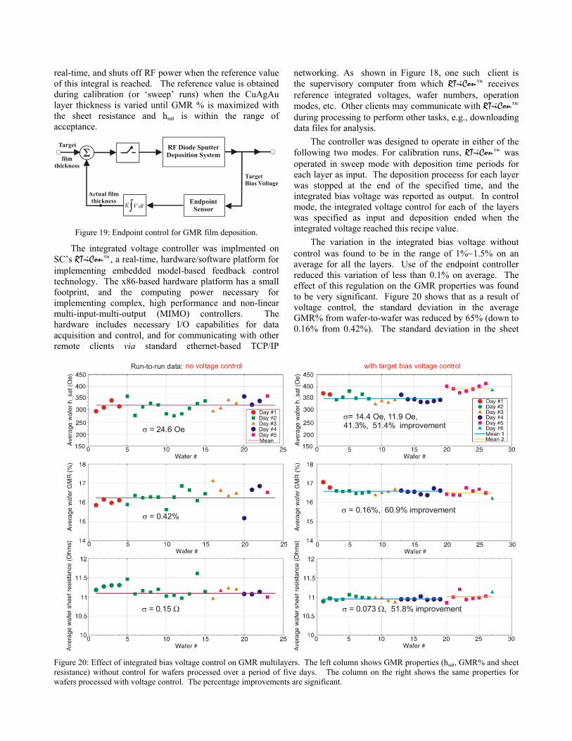
real-time, and shuts off RF power when the reference value of this integral is reached. The reference value is obtained during calibration (or ‘sweep’ runs) when the CuAgAu layer thickness is varied until GMR % is maximized with the sheet resistance and hsat is within the range of acceptance.
TargetBias Voltage
RF Diode SputterDeposition System
Actual filmthickness Endpoint
Sensor
Target
V dtK
Figure 19: Endpoint control for GMR film deposition.
The integrated voltage controller was implmented on SC’s RT-iCon™, a real-time, hardware/software platform for implementing embedded model-based feedback control technology. The x86-based hardware platform has a small footprint, and the computing power necessary for implementing complex, high performance and non-linear multi-input-multi-output (MIMO) controllers. The hardware includes necessary I/O capabilities for data acquisition and control, and for communicating with other remote clients via standard ethernet-based TCP/IP
networking. As shown in Figure 18, one such client is the supervisory computer from which RT-iCon™ receives reference integrated voltages, wafer numbers, operation modes, etc. Other clients may communicate with RT-iCon™ during processing to perform other tasks, e.g., downloading data files for analysis.
The controller was designed to operate in either of the following two modes. For calibration runs, RT-iCon™ was operated in sweep mode with deposition time periods for each layer as input. The deposition proceess for each layer was stopped at the end of the specified time, and the integrated bias voltage was reported as output. In control mode, the integrated voltage control for each of the layers was specified as input and deposition ended when the integrated voltage reached this recipe value.
The variation in the integrated bias voltage without control was found to be in the range of 1%−1.5% on an average for all the layers. Use of the endpoint controller reduced this variation of less than 0.1% on average. The effect of this regulation on the GMR properties was found to be very significant. Figure 20 shows that as a result of voltage control, the standard deviation in the average GMR% from wafer-to-wafer was reduced by 65% (down to 0.16% from 0.42%). The standard deviation in the sheet
with target bias voltage control
σ Ω= 0.073 , 51.8% improvement
σ = 0.16%, 60.9% improvement
σ= 14.4 Oe, %, 51.4% improvement
11.9 Oe,41.3
Run-to-run data: no voltage control
σ = 24.6 Oe
σ = 0.42%
σ Ω= 0.15
Figure 20: Effect of integrated bias voltage control on GMR multilayers. The left column shows GMR properties (hsat, GMR% and sheet resistance) without control for wafers processed over a period of five days. The column on the right shows the same properties for wafers processed with voltage control. The percentage improvements are significant.
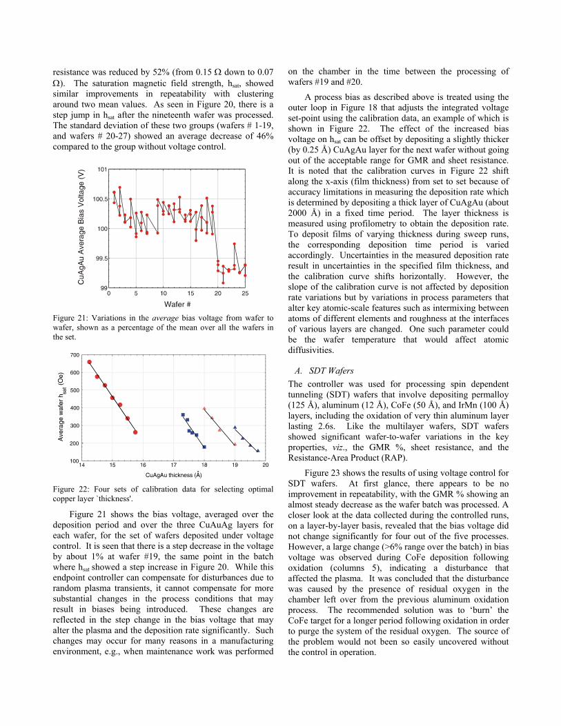
resistance was reduced by 52% (from 0.15 Ω down to 0.07 Ω). The saturation magnetic field strength, hsat, showed similar improvements in repeatability with clustering around two mean values. As seen in Figure 20, there is a step jump in hsat after the nineteenth wafer was processed. The standard deviation of these two groups (wafers # 1-19, and wafers # 20-27) showed an average decrease of 46% compared to the group without voltage control.
Figure 21: Variations in the average bias voltage from wafer to wafer, shown as a percentage of the mean over all the wafers in the set.
Figure 22: Four sets of calibration data for selecting optimal copper layer `thickness'.
Figure 21 shows the bias voltage, averaged over the deposition period and over the three CuAuAg layers for each wafer, for the set of wafers deposited under voltage control. It is seen that there is a step decrease in the voltage by about 1% at wafer #19, the same point in the batch where hsat showed a step increase in Figure 20. While this endpoint controller can compensate for disturbances due to random plasma transients, it cannot compensate for more substantial changes in the process conditions that may result in biases being introduced. These changes are reflected in the step change in the bias voltage that may alter the plasma and the deposition rate significantly. Such changes may occur for many reasons in a manufacturing environment, e.g., when maintenance work was performed
on the chamber in the time between the processing of wafers #19 and #20.
A process bias as described above is treated using the outer loop in Figure 18 that adjusts the integrated voltage set-point using the calibration data, an example of which is shown in Figure 22. The effect of the increased bias voltage on hsat can be offset by depositing a slightly thicker (by 0.25 Å) CuAgAu layer for the next wafer without going out of the acceptable range for GMR and sheet resistance. It is noted that the calibration curves in Figure 22 shift along the x-axis (film thickness) from set to set because of accuracy limitations in measuring the deposition rate which is determined by depositing a thick layer of CuAgAu (about 2000 Å) in a fixed time period. The layer thickness is measured using profilometry to obtain the deposition rate. To deposit films of varying thickness during sweep runs, the corresponding deposition time period is varied accordingly. Uncertainties in the measured deposition rate result in uncertainties in the specified film thickness, and the calibration curve shifts horizontally. However, the slope of the calibration curve is not affected by deposition rate variations but by variations in process parameters that alter key atomic-scale features such as intermixing between atoms of different elements and roughness at the interfaces of various layers are changed. One such parameter could be the wafer temperature that would affect atomic diffusivities.
A. SDT Wafers The controller was used for processing spin dependent tunneling (SDT) wafers that involve depositing permalloy (125 Å), aluminum (12 Å), CoFe (50 Å), and IrMn (100 Å) layers, including the oxidation of very thin aluminum layer lasting 2.6s. Like the multilayer wafers, SDT wafers showed significant wafer-to-wafer variations in the key properties, viz., the GMR %, sheet resistance, and the Resistance-Area Product (RAP).
Figure 23 shows the results of using voltage control for SDT wafers. At first glance, there appears to be no improvement in repeatability, with the GMR % showing an almost steady decrease as the wafer batch was processed. A closer look at the data collected during the controlled runs, on a layer-by-layer basis, revealed that the bias voltage did not change significantly for four out of the five processes. However, a large change (>6% range over the batch) in bias voltage was observed during CoFe deposition following oxidation (columns 5), indicating a disturbance that affected the plasma. It was concluded that the disturbance was caused by the presence of residual oxygen in the chamber left over from the previous aluminum oxidation process. The recommended solution was to ‘burn’ the CoFe target for a longer period following oxidation in order to purge the system of the residual oxygen. The source of the problem would not been so easily uncovered without the control in operation.
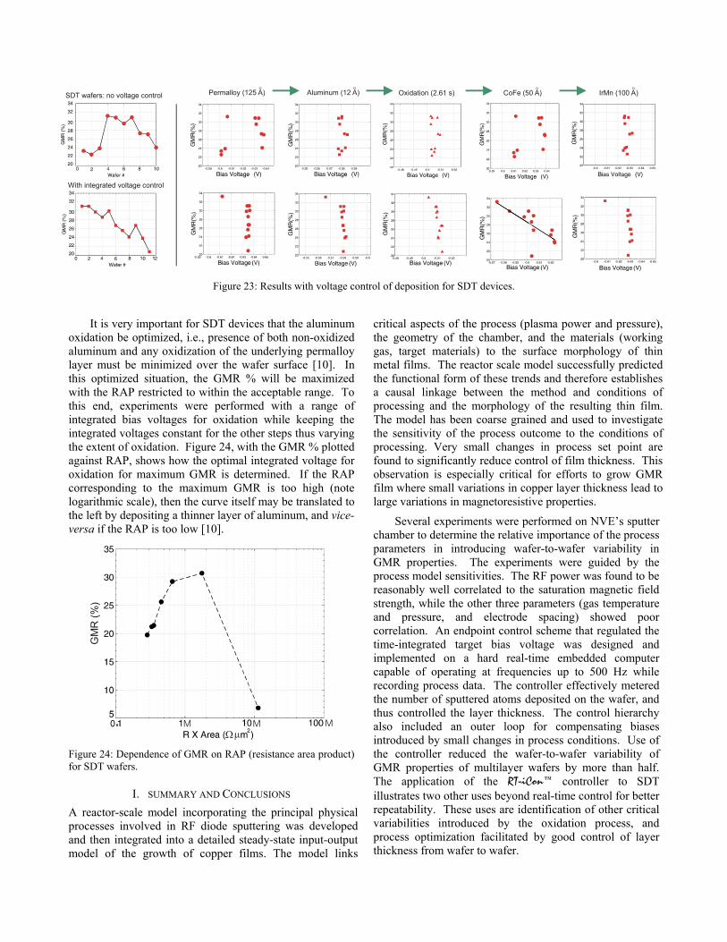
Permalloy (125 A) Aluminum (12 A) Oxidation (2.61 s) CoFe (50 A) IrMn (100 A)O OOO
SDT wafers: no voltage control
With integrated voltage control
Figure 23: Results with voltage control of deposition for SDT devices.
It is very important for SDT devices that the aluminum
oxidation be optimized, i.e., presence of both non-oxidized aluminum and any oxidization of the underlying permalloy layer must be minimized over the wafer surface [10]. In this optimized situation, the GMR % will be maximized with the RAP restricted to within the acceptable range. To this end, experiments were performed with a range of integrated bias voltages for oxidation while keeping the integrated voltages constant for the other steps thus varying the extent of oxidation. Figure 24, with the GMR % plotted against RAP, shows how the optimal integrated voltage for oxidation for maximum GMR is determined. If the RAP corresponding to the maximum GMR is too high (note logarithmic scale), then the curve itself may be translated to the left by depositing a thinner layer of aluminum, and vice-versa if the RAP is too low [10].
Ω µ
GM
R (%
)
M. M M
Figure 24: Dependence of GMR on RAP (resistance area product) for SDT wafers.
I. SUMMARY AND CONCLUSIONS A reactor-scale model incorporating the principal physical processes involved in RF diode sputtering was developed and then integrated into a detailed steady-state input-output model of the growth of copper films. The model links
critical aspects of the process (plasma power and pressure), the geometry of the chamber, and the materials (working gas, target materials) to the surface morphology of thin metal films. The reactor scale model successfully predicted the functional form of these trends and therefore establishes a causal linkage between the method and conditions of processing and the morphology of the resulting thin film. The model has been coarse grained and used to investigate the sensitivity of the process outcome to the conditions of processing. Very small changes in process set point are found to significantly reduce control of film thickness. This observation is especially critical for efforts to grow GMR film where small variations in copper layer thickness lead to large variations in magnetoresistive properties.
Several experiments were performed on NVE’s sputter chamber to determine the relative importance of the process parameters in introducing wafer-to-wafer variability in GMR properties. The experiments were guided by the process model sensitivities. The RF power was found to be reasonably well correlated to the saturation magnetic field strength, while the other three parameters (gas temperature and pressure, and electrode spacing) showed poor correlation. An endpoint control scheme that regulated the time-integrated target bias voltage was designed and implemented on a hard real-time embedded computer capable of operating at frequencies up to 500 Hz while recording process data. The controller effectively metered the number of sputtered atoms deposited on the wafer, and thus controlled the layer thickness. The control hierarchy also included an outer loop for compensating biases introduced by small changes in process conditions. Use of the controller reduced the wafer-to-wafer variability of GMR properties of multilayer wafers by more than half. The application of the RT-iCon™ controller to SDT illustrates two other uses beyond real-time control for better repeatability. These uses are identification of other critical variabilities introduced by the oxidation process, and process optimization facilitated by good control of layer thickness from wafer to wafer.
ACKNOWLEDGEMENT The authors would like to thank Professor H. Wadley and Dr. W. Zou at the University of Virginia, Charlottesville, for their valuable help with modeling. They greatly appreciate the help of D. Brownell and Dr. D. Wang of NVE, Inc., Eden Prairie, MN where the experimental work was performed. They are grateful for the active interest and support of Dr. A. Tsao and Dr. S. Wolf at DARPA.
REFERENCES [1] Levy, P. M., Giant Magneto-Resistance in Magnetic Layers,
Solid-State Physics, Advances in Research and Application, Volume 47, Academic Press, San Diego, 1994.
[2] Daughton, J. M. and Y. J. Chen, GMR Materials for Low Field Applications, IEEE Transactions on Magnetics, Vol. 29, No.6, November 1993.
[3] Schlichting, H., Boundary-Layer Theory, 7th ed. McGraw-Hill, New York, 1979.
[4] S. Desa, S. Ghosal, R. L. Kosut, J. L. Ebert, T. E. Abrahamson, A. Kozak, D. W. Zou, X. Zhou, J. F. Groves, and H. N. G. Wadley, ‘Reactor-Scale Models for RF-Diode Sputtering of Metal Thin Films’, Journal of Vacuum Science & Technology A, Vol. 17, No.4, pp. 1926-1933, 1999.
[5] Lieberman, M. A., and A. L. Lichtenberg, Principles of Plasma Discharges and Materials Processing, John Wiley and Sons, New York, 1994.
[6] National Instruments, Inc., Matrixx Product Family Users Manuals, Austin, TX, 2004.
[7] Urbassek, H. M., Molecular-dynamics simulation of sputtering, Nuclear Instruments and Methods in Physics Research B 122, pages 427-441, 1997.
[8] Groves, J. F., Directed Vapor Deposition, Ph. D. Dissertation, University of Virginia, 1998.
[9] Bird, G. A., Molecular Gas Dynamics and the Direct Simulation of Gas Flows, Clarendon Press, New York, 1994.
[10] Song, J. Nowak, and M. Covington, ‘Proper Oxidation for Spin Dependent Tunneling Junctions’, 44th Annual Conference of Magnetism and Magnetic Materials, November 1999, San Jose.