Multimoded RF Systems for Future Linear...
131
Multimoded RF Systems for Future Linear Colliders Sami G. Tantawi
Transcript of Multimoded RF Systems for Future Linear...

Multimoded RF Systems for Future Linear Colliders
Sami G. Tantawi

AcknowledgmentThis work is a result of a continuous effort by many researches and engineers over many years.
In particular, The efforts of C. Nantista, N. Kroll, R. Miller, P. Wilson, V. Dolgashev, K. Fant, C. Pearson, R. Ruth, were instrumental to the results achieved to date.
Jose Chan: A persistence efforts during the manufacturing and testing of components
David Schultz Denis Atkinson, C. Adolphsen D. Burke and the NLC group
J. Nelson, K. Jobe, M. Ross, J. Frisch, T. Smith, D. McCormick, and the NLCTA operations team were a must for the successful conclusion of this project.
D. Cassel, J. DeLamare, M. Nguyen, M. Laruss and the modulator team
K. Ratcliffe and the Vacuum Assembly Team.
We wish to Thank all operators that took shifts 24 hours a day for several months

Outline
• Dualmode resonant delay line pulse compression system for the Next Linear Collider (NLC)
1. Introduction2. Components: design and cold tests3. Dualmode Delay Lines: Design and
Experimental results4. High power experimental results

RF Accelerator Structures needs a short, high power, rf
pulse. For example the current NLC design requires a flat-top
396 ns rf pulse with a power level of about 95 MW/m at 11.424 GHz, and
a repetition rate of 120 Hz to feed each accelerator structure.
One need to transfer the CW wall plug power to rf pulses with high
power and low duty factor. Hence
1. A storage system is needed.
2. A Switch or a switching mechanism is needed to control the charging and
discharging of the system.
3. A device to generate the RF power

Storage Systems:1. Capacitors; i.e. Modulators.
Switches include pulse forming networks, thyrotrons, IGBTs, and grided guns on microwave tubes.
2. Kinetic energy of an electron beam ; i.e. two beam accelerator, Switches include RF beam kickers
3. In the accelerator structure; i.e. super conducting accelerators.
4. In rf transmission lines and cavities; i.e. rf pulse compression systems. Switches includes rf phase manipulation between rf sources, andsolid state switches.

In general most of rf systems, suggested for a linear collider, contains elements from several of the above storage system.
To compare these system one has to consider: 1- Philosophy of the design
• Modularity: one may choose to have a unit that contains one rf source, and compact pulse compression system such as SLED-II• Flexibility in the operating rf frequency: one may choose Two beam systems•…..
2- Efficiency3- Cost

The choice of the system is greatly affected by the available technology of the components.
If one has
1- A really inexpensive efficient rf source
2- A a very efficient and inexpensive modulator system using a very fast switch (such as grided gun on the rf source)
One might use several thousands of these devices to power the main Linac of a collider
However, neither the inexpensive rf source nor the very fastmodulator exist, only ideas at the moment.

The need for RF Pulse compression
1- It is usually easier to build rf sources with low power and long pulse width. 2- Rf sources are expensive, one should get as much energy from them as possible, i.e., the longest possible pulse. One should not let an expensive rf source in an idle mode most of the time.
Hence, rf pulse compression is needed to match the long pulse low power of available rf sources such as klystrons to the high power short pulse needed for the accelerator structure.

• Pulse Compression should be used with as high of a compression ratio as possible until
a) The cost of the compression system starts to exceed that of the klystrons and modulator
b) Or, the available pulse width of the klystrons is exhausted
• The cost of the main linac is directly proportional to the efficiency of the pulse compression system.

RF Pulse compression for RF Linacs and Colliders
• Resonance Delay Lines (SLED-II)• Binary Pulse Compression (BPC)• Delay Line Distribution System (DLDS)
• Two-Stage systems, any combination of two or more of the above systems

klystrons
Single or Multi-Moded Delay Lines
Short Circuit
Coupling Irises
Accelerator Structures
3 dB 90 Degree Hybrid
Sled-II Pulse compression system
klystrons
Single or Multi-Moded Delay Lines
Short Circuit
Coupling Irises (can be actively switched)
Circulator
Accelerator Structures
Sled-II pulse compression system with a circulator and active switches

Single-Moded Delay Lines
3 dB 90 Degree Hybrid
Accelerator Structure
Two banks of power sources each has an nk/2 klystrons
a) Single-moded Binary Pulse Compression
3 dB 90 Degree Hybrid
Accelerator Structure
Two banks of power sources each has an nk/2 klystrons
Single or Multi-Moded Delay Lines
Circulator
Short Circuit
b) Binary pulse compression can have several improvements including the use of a circulator and several modes to reduce the delay line length.

Delay Lines
Accelerator StructuresBank of nk of klystrons
A set of hybrids that switches the combined rf to different outputs
Not all the output need to be used. The unused outputs are terminated by an rf load
a) A Unit of a Single-Moded DLDS
Multi-Moded Delay Lines. The total number of these lines is np
A mode launcher which takes nm inputs and produces nm modes into a single waveguide delay line
b) A Unit of a Multi-Moded DLDS
Single-Moded Delay Lines
Accelerator Structures
A combinerA High Power Microwave Switch
c) A Unit of an Active DLDS

The challenges facing most of these pulse compression system are
1- Compactness, how to produce a storage system which is relatively compact
2- Efficiency, for the resonant delay lines, efficiency could be boosted by an rf switch.
3- Most of these systems could have a more compact topology if one have, a nonreciprocal RF device (circulator), or a switch.

Compactness
•A waveguide near cutoff, hence, a low group velocity. One can use a higher order mode to reduce the losses. A bad idea, dispersion will destroy the pulse shape at a group velocity less than 4.
•Loaded waveguide (slow wave structure). A bad idea because of dispersion and losses.
•Multimoded Waveguide, the only good idea with no draw backs. We are using highly overmoded waveguide systems no mater what, using an extra mode, or two, or four, .. Is a bonus.

0.5
0.6
0.7
0.8
0.9
1
1.1
1.2
4 6 8 10 12 14 16
Single Moded DLDSMulti-Moded DLDS (number of modes=3)Active DLDSMulti-Moded BPC (A high power circulator and 3 modes)Multi-Moded SLED II (A high power circulator and 3 modes) Active SLED II (One time Switching [7])Multi-Moded DLDS (n
k=4, number of modes =3)
Single-Moded DLDS (nk=4)
Rel
ativ
e C
ost
Compression Ratio
nk=8

0
20
40
60
80
100
0 200 400 600 800 1000 1200 1400
Ele
ctric
Fie
ld (M
V/m
)
Pulse Width [ns]
Electric Field breakdown strength in a 16% Group velocity copper waveguide at 11.424 GHz
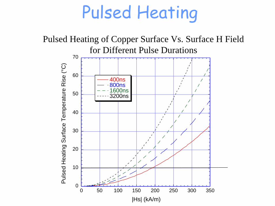
Pulsed Heating
0
10
20
30
40
50
60
70
0 50 100 150 200 250 300 350
400ns800ns1600ns3200ns
Pul
sed
Hea
ting
Sur
face
Tem
pera
ture
Ris
e (°
C)
|Hs| (kA/m)
Pulsed Heating of Copper Surface Vs. Surface H Field for Different Pulse Durations

Dualmode Resonant Delay lines ~30m
RF Input to the 4 50 MW klystrons
Single mode waveguide input to the pulse compression system; 100 MW/Line for 1.6 µs
Dual mode waveguide carrying 200 MW
Compressed output > 600 MW 400 ns.
Output Load Tree
NLC experimental rfpulse compression
system

Dualmode CombinerTwo fundamental
mode inputs
TE10/TE20
TE01/TE11
Dualmode directional coupler
Pumpout
Super Hybrid
TE01 to delay Lines
TE01/TE11 to loads
The Head of the pulse compression system

Dual-Mode Combiner
@ 600 MW |Esmax| = ~45.7 MV/m
|Hsmax| = ~218 kA/m
@ 600 MW |Esmax| = ~31.5 MV/m
|Hsmax| = ~73.9 kA/m
TE10
TE20

Dual-Mode Combiner/Splitter
@ 600 MW |Esmax| = ~45.7 MV/m
|Hsmax| = ~218 kA/m
@ 600 MW |Esmax| = ~31.5 MV/m
|Hsmax| = ~73.9 kA/m

139.8 mm
40.64 mm
36.45 mm
30.58 mm
WC160
Section#1
Section#2
Section#3
Width taper to match our standard overmoded waveguide
36.63 mm

TE01
TE20
TE10
TE11

TE01
TE20
TE10
TE11
Simulated electric fields (HFSS)of the multi-moded circular to rectangular taper
139.8 mm
Taper Geometry (Operating Frequency=11.424 GHz)
40.64 mm
36.45 mm 36.63 mm
Dual-Moded Rectangular Circular Converter/Tapers

TE01
TE20
TE10
TE11
DualmodeRectangular-to-Circular
Taper

Instrumental components for cold testing of multimode components:
1. TE11 Mode launcher2. TE01 Mode launcher3. Width taper4. Height taper5. Small waveguide sections with different lengths at all
waveguide cross sections
We followed a strict methodology of designing these instruments. They had to be simulated with at least three different codes and have a performance that is much better than any component that we have. Of course we can only do that because there is no restrictions on field levels.

Cold Test Components/Calibration Standards
Width Taper, Height Tapers and Jog Mode Converter
TE01 Mode Converter, TE11 Mode Converter, and Size Taper
Multimoded Matched Load

11.324 11.357 11.391 11.424 11.457 11.491 11.5240.9
0.91
0.92
0.93
0.94
0.95
0.96
0.97
0.98
0.99
1
before modificationafter modification
Frequency [GHz]
S12
Measured S12 between the Rectangular TE02 mode and the circular TE01mode. These measurements include the response of mode transducers
necessary to launch the modes at both ends of the taper.

0.9
0.92
0.94
0.96
0.98
1
11.324 11.374 11.424 11.474 11.524
S12
Frequency (GHz)
Measured S12 between the rectangular TE01 mode and the circular TE11 mode. These measurements include the response of mode transducers necessary to launch the modes at
both ends of the taper.

To instrumental width taper-To instrumental height taper-To Network analyzer
To instrumental width taper-To instrumental height taper-To Network analyzer
TE01 Mode launcher
From Network Analyzer
Cold Test Setup for the Splitter and Circular-to-Rectangular Taper
TE20 Mode
3
2
1

170
175
180
185
190
11.3 11.35 11.4 11.45 11.5 11.55
Phase diiference between S21
and S31
Phas
e (d
egre
es)
Frequency (GHz)
-4
-3.8
-3.6
-3.4
-3.2
-3
11.274 11.324 11.374 11.424 11.474 11.524 11.574
S21
S31
Mag
nitu
ed (d
B)
Frequency (GHz)
Cold Test Results of:Splitter-Circular to rectangular taper-Wraparound mode converter-instrumental height taper-instrumental width taper. Total losses at 11.424 GHz =1.3%

Jog Converter and Mode Mixer
1.442”TE10 TE10
orthogonal 50/50 mixesTE20
TE20

Magic H Hybrid
0.900”
2.3821”
1.4788”
@ 600 MW, 1.435” height: |Esmax| = ~45.6 MV/m
|Hsmax| = ~168 kA/m
C. Nantista ‘02

TE10
straight through
TE02
To the pulse compressor
@ 516 MW,
|Esmax| = ~45.8 MV/m
|Hsmax| = ~156 kA/m To/From Pulse
Compressors
Jog-ConverterCombiner/Splitter
Planer 3-dB Hybrid

Jog mode mixer
Combiner/Splitter
Planer 3-dB Hybrid
Planer Super-Hybrid
Port 1
Port 4
Port 3
Port 2
Circular to Rectangular Tapers
Jog-mode converter
Mitered Bends

-0.5
-0.4
-0.3
-0.2
-0.1
0
11.404 11.414 11.424 11.434 11.444
ports 2&3 shortedport 2 openports 2&3 openTE
11 T
rans
mis
sion
(dB
)
Frequency (GHz)
Circular TE11 mode transmission and reflection between port 1 and port 4 (S41) for different
conditions at port 2 and port 3.
Port 1
Port 4Port 3
Port 2
-60
-50
-40
-30
-20
-10
0
11.324 11.374 11.424 11.474 11.524
ports 2&3 shortedport 2 openports 2&3 open
TE11
Ref
lect
ion
(dB
)
Frequency (GHz)

-60
-50
-40
-30
-20
-10
0
11.404 11.414 11.424 11.434 11.444
initialspacer added to input
TE01
Ref
lect
ion
(dB)
Frequency (GHz)
Port 1
Port 4Port 3
Port 2
Reflection measurements (S11) for the circular TE01 mode from port 1 while shorting both port 2 and port 3 and matching port 4.

Port 1
Port 4Port 3
Port 2
-0.5
-0.45
-0.4
-0.35
-0.3
-0.25
-0.2
-0.15
-0.1
11.404 11.414 11.424 11.434 11.444
TE01
Tra
nsm
issi
on (d
B)
Frequency (GHz)
Circular TE01 mode transmission between port 1 and port 4 (S41) while shorting both port 2 and port 3.

1.442”
@ 600 MW |Esmax| = ~37.8 MV/m
|Hsmax| = ~83.8 kA/m
Bend Converter Design

Dual-Mode Splitter
TE01 or TE11
TE10
TE01
TE20bend converter
Dualmode Splitter: For either incident mode the power is evenly divided between the two output ports, which launch the TE01.

Load Tree: The input power, carried by the TE01 mode, is split 4 ways to be absorbed at the loads

WC160
|S11| < -57 dB @ 11.424 GHz
Four Way Splitter DesignWR90

-7
-6.5
-6
-5.5
11.324 11.374 11.424 11.474 11.524
Power Divider
Port 1Port 2
Port 3Port 4
dB
Frequency (GHz)

-35
-30
-25
-20
-15
-10
11.324 11.374 11.424 11.474 11.524
Circular Port
dB
Frequency (GHz)

High Power Load Design

Rectangular waveguide for coupling the TE01 mode
Ridge waveguide for coupling the TE11 mode
Circular Waveguide
•The waveguide sizes are chosen to match wavelengths between the circular waveguide modes and side waveguide fundamental mode
•The coupling hole pattern represents a Hamming window
Dual-moded Directional Coupler

End taper for TE11 coupler

End taper for the TE01 coupler

Directional Coupler Cold Test

-125
-120
-115
-110
-105
-100
-95
-90
-85
11.174 11.299 11.424 11.549 11.674
Coupling between the TE01
mode and the TE11
coupler arm
dB
Frequency (GHz)
Since the coupling coefficient for the desired mode is -47 dB, Isolation between coupler arm and the unwanted mode is better than -45 dB.

Measured directivity for the TE01 Arm

Pumpout design: the set of holes are designed to cancel any coupling orself-coupling for the TE01 and the TE11

Vacuum Pumpout Cold Test
0
0.05
0.1
0.15
0.2
0.25
0.3
11.35 11.4 11.45 11.5
WC159 Vacuum Pumpout Match
TE11TE01
Am
plitu
de o
f S11
Frequency (GHz)
0.86
0.88
0.9
0.92
0.94
0.96
0.98
1
11.35 11.4 11.45 11.5
WC159 Vacuum Pumpout Transmission
TE11TE01
Frequency (GHz)
Am
plitu
de o
f S21

TE01
TE02
TE02
TE01
Dual Moded Delay line occupy only half the length of a single moded delay line

Dual-Moded Delay LineDual-moding the delay lines cuts their required length approximately in half.
21
21
2 gg
gg
vvvvTL+
=
input taper
17.08 cm delay line ~29 m long
end taper
TE01
TE02
TE02
TE01
mode converter / tuning short

R=4.1275cm
vacuum feed-through plunger
TE01(TE02)
⎟⎟⎟⎟⎟⎟⎟
⎠
⎞
⎜⎜⎜⎜⎜⎜⎜
⎝
⎛
−−−
−−−
=
θθθ
θθθ
θθθ
φφ
φφ
cos2
sin2
sin2
sin2cos
2cos
2sin
2cos
2cos
jj
jj
ee
ee
S
Reflective TE01/TE02 Mode Converter
TE02(TE01)
S =

⎟⎟⎟⎟⎟⎟⎟
⎠
⎞
⎜⎜⎜⎜⎜⎜⎜
⎝
⎛
−−−
−−−
=
θθθ
θθθ
θθθ
φφ
φφ
cos2
sin2
sin2
sin2cos
2cos
2sin
2cos
2cos
jj
jj
ee
ee
S
1.932” 3.25”
1.045”
Field Pattern within the device. Peak field at 300 MW (one device per transmission line) is 26.6 MV/m. This field is in the middle of the small guide.
TE01
TE02
TE02
TE01

End mode converter simulations
TE01 TE02 End taper and mode converter

-0.1
-0.08
-0.06
-0.04
-0.02
0
11.324 11.374 11.424 11.474 11.524
TE01 Transmitted TE02 Transmission
dB
Frequency [GHz]
End Taper (before the TE01-TE02 Mode converter)

Input taper design

-1
-0.8
-0.6
-0.4
-0.2
0
11.3 11.35 11.4 11.45 11.5 11.55
TE01 Transmitted TE02 Reflection
dB
Frequency [GHz]
Input Taper for a Dual-Moded System

0
0.2
0.4
0.6
0.8
1
1.2
-200 -100 0 100 200 300 400 500
Reflected PulseInput Pulse
Mag
nitu
de
Time [ns]
Measured Delay through 75 feet of WC475 waveguide terminated with a flat plate. The round trip delay time is 154 ns
0
0.2
0.4
0.6
0.8
1
1.2
-200 -100 0 100 200 300 400 500
InputPulse Mag
Mag
nitu
de
Time [ns]
Measured delay through 75 feet of WC475 waveguide terminated with a TE01-TE02 Mode converter. The round trip delay time is 320 ns

Multimoded Taper Cold Test

0
0.2
0.4
0.6
0.8
1
11.3 11.35 11.4 11.45 11.5 11.55
, p p p p
Dat
a M
ag
Freq GHz
S11 M
agnitude
-0.2
0
0.2
0.4
0.6
0.8
1
1.2
-300 -200 -100 0 100 200 300
Output pulse (delayed by 15 ns 4 round trips)Input pulse
Pul
se M
agTime(ns)
Pulse Am
plitude
Measured frequency response and constructed time response of the dual-moded taper assembly.

Measured Response of the dual-mode SLED-II Pulse compression system at a compression ratio of 4. Delay line length is ~35 feet. Output pulse width is 150 ns.
0
0.5
1
1.5
2
2.5
3
3.5
4
0 125 250 375 500 625 750 875
Compressed Pulse Input
Rel
ativ
e Po
wer
Time (ns)

Delay Line Cold Tests

Delay Line Cold Tests
-1.5
-1
-0.5
0
0.5
1
1.5
2
-1000 -500 0 500 1000
sled9
Pulse MagInput
-1.5
-1
-0.5
0
0.5
1
1.5
2
-1000 -500 0 500 1000
p1sled2
Pulse MagInputtop line bottom line
Small mid-time-bin steps seen (mode impurity).

0
0.01
0.02
0.03
0.04
0.05
0.06
0
30
60
90
120
210
240
270
300
330
Bottom LineTop Line
Ref
lect
ion
0
0.01
0.02
0.03
0.04
0.05
0.06
-12 -8 -4 0 4 8 12
Bottom LineTop Line
1st R
ound
Trip
Ref
lect
ion
Am
plitu
de (n
o iri
s)
Mode Converter Cup Position (mm)
TE01 mode contamination
bottom line: ~-34 dB
top line: ~-26 dB
Amplitude oscillation due to interference with slight wrap-around mode launcher mismatch (~-48 dB).
Spurious reflection after first round trip (irises removed)

Amp. ∆φ/∆L ∆Lcup error TE01
TE02+δTE01TE02+δTE01
TE01
2β01
TE02
const. 2β01
line/taper error
(β01+β02)
TE01+δTE02
TE02+δTE01
TE01
TE02+δTE01+δTE01(β01+β02)(β02+β01)
TE02
const.
The wavelengths for these phase oscillations are 14.2 mm and 16.1 mm, respectively.
Measurements show a phase cycle over ~ 16 mm, indicating mode contamination predominantly from the delay lines and tapers.
Slight amplitude oscillations reveal a very small fixed mismatch in wrap-around mode launcher.
Non-periodic amplitude change can be attributed to longer range beating between a small cup error contamination and that from the lines/tapers (60.3 mm).

Problem Fixed by:
•Permutations of tapers
•Adjusting iris distance
•Choosing good resonant position for tuning plunger (3 within range of motion).
0
0.5
1
1.5
2
2.5
3
3.5
-1000 -500 0 500 1000
Pulse MagInput
Pow
er G
ain
Time (ns)
Top Line
0
0.5
1
1.5
2
2.5
3
3.5
-1000 -500 0 500 1000
Pulse MagInput
Pow
er G
ain
Time (ns)
Bottom Line

System test (1)
Input
output
0
0.5
1
1.5
2
2.5
3
-1000 -500 0 500 1000
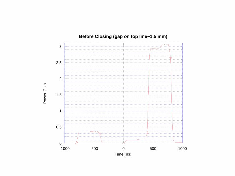
Before Closing (gap on top line~1.5 mm)
Pow
er G
ain
Time (ns)

0
0.2
0.4
0.6
0.8
1
1.2
1.4
-1000 -500 0 500 1000
Signal Amplitudes at the Launcher
Pulse MagPulse Mag
Pul
se M
ag
Time (ns)

0
0.4
0.8
1.2
1.6
2
2.4
2.8
3.2
-1000 -500 0 500 1000
Total System Response
Pow
er G
ain
Time (ns)

88
88.2
88.4
88.6
88.8
89
450 500 550 600 650 700 750 800 850
Phase of output pulse
Pha
se (D
egre
es)
Time (ns)

0
0.4
0.8
1.2
1.6
2
2.4
2.8
3.2
-1000 -500 0 500 1000
Measurments Throgh The TE01 Arm of the Directional Coupler
Pow
er G
ain
Time (ns)

0
0.005
0.01
0.015
0.02
-1000 -500 0 500 1000 1500 2000
Reflected PowerInput
Ref
lect
ed P
ower
Time (ns)

0
0.0005
0.001
0.0015
0.002
0.0025
-1000 -500 0 500 1000
Power Seen at the TE11 Arm
Pow
er
Time (ns)

0
0.4
0.8
1.2
1.6
2
2.4
2.8
3.2
-1000 -500 0 500 1000
Comparison between the signal seen at the TE11 Arm with the signal at the TE01 Arm
103 x Measured Power at the TE11 ArmMeasured Power at the TE01 Arm
Pow
er
Time (ns)

Input
output
System test (2)

0
0.5
1
1.5
2
2.5
3
-1 -0.5 0 0.5 1
before removing the spacer
Pulse MagPulse MagInput
Pul
se M
ag
Time
System Cold Tests
-90
-88
-86
-84
-82
-80
-78
-76
11.404 11.414 11.424 11.434 11.444
dB
Freq GHz
-7
-6
-5
-4
-3
-2
-1
0
11.404 11.414 11.424 11.434 11.444
leftcomb_nospacer-53-95avg
Dat
a M
ag
Freq GHz
spacer in
spacer removed
resonance between combiner and SLED head

16 steps 2 klystrons

High Power Experiments

8-Pack Phase 1

After pulse breakdown(Loads)

Upper Delay Line end pump

Upper Delay Line Input Pump

0
5 107
1 108
1.5 108
2 108
2.5 108
3 108
3.5 108
4 108
0 5 10-7 1 10-6 1.5 10-6 2 10-6
400MWpoint100ns
Channel 1Channel 2
Cha
nnel
1
Time

0
5 107
1 108
1.5 108
2 108
2.5 108
3 108
3.5 108
4 108
0 5 10-7 1 10-6 1.5 10-6 2 10-6
383MW216ns
BC
B
A

Zero Power

421 MW 360 ns

Dualmode Resonant Delay lines ~30m
RF Input to the 4 50 MW klystrons
Single mode waveguide input to the pulse compression system; 100 MW/Line for 1.6 µs
Dual mode waveguide carrying 200 MW
Compressed output > 600 MW 400 ns.
Output Load Tree
NLC experimental rfpulse compression
system

System Modifications
• Replaced a pumpout• Replaced the whole line of WR90• Cooled down the WR90 with fans• Hard wired the klystrons driver together

Dualmode Resonant Delay lines ~30m
RF Input to the 4 50 MW klystrons
Single mode waveguide input to the pulse compression system; 100 MW/Line for 1.6 µs
Dual mode waveguide carrying 200 MW
Compressed output > 600 MW 400 ns.
Output Load Tree
NLC experimental rfpulse compression
system


436 MW 360 ns

0
100
200
300
400
500
600
0 0.5 1 1.5 2
InputOutput
Pow
er (M
W)
Time(µs)
Dualmoded SLED-II Performance December 4, 2003 11 amTE
01-Input TE
01-Output

0
100
200
300
400
500
600
0 0.5 1 1.5 2
InputOutput
Pow
er (M
W)
Dualmoded SLED-II Performance December 6, 2003 1:00 am
TE01
-Input TE01
-Output
Time(µs)

0
100
200
300
400
500
600
0 0.5 1 1.5 2
Input
OutputPo
wer
(MW
)
Dualmoded SLED-II ProcessingTE
01-Input TE
01-Output
Time(µs)

0
100
200
300
400
500
600
0 0.5 1 1.5 2
Pow
er (M
W)
T im e (µs)
Input
O utput

0
2
4
6
8
10
250 300 350 400 450 500 550
Error=100 x (Detector M easurem ent-Calorim etric M easurem ent)/ Detector M easurem ent
Erro
r (%
)
Power (M W )---Detector

Klystron 1
Klystron 4
Klystron 3
Klystron 2
φ
φ
φ
TWT1
TWT2
119 MHzPLL to 11.424 GHz
Timing Switch
Voltage-controlled Switch
Bi-phase Modulator
IQ-Modulator
AFG 1
AFG 1
Computer Data AcquisitionFrom High Power rf measurements
Low-Level RF Architecture


Multimoded SLED-II output with feedback
0
100
200
300
400
500
600
0 0.5 1 1.5 2
InputOutput
Pow
er (M
W)
Time (µs)Sami Tantawi (1/27/2004)

0
37
74
111
148
185
-0.5 0 0.5 1 1.5 2 2.5 3
txt_output
B

176
178
180
182
184
1.7 1.75 1.8 1.85 1.9 1.95 2 2.05 2.1
txt_output
B

500
505
510
515
520
525
530
1.4 1.5 1.6 1.7 1.8 1.9
InputOutput
Pow
er (M
W)
Time (µs)Sami Tantawi (1/27/2004)

60 Hz
Full Run One Minute Power Data
~455.7 hrs. on total w/ ~272 trips*~98.75 hrs. @ 60 Hz w/ ~ 116 trips
~357 hrs. @ 30 Hz w/ ~ 156 trips
30 Hz
Two 26 hrs. gaps w/ no trips.
trip diode signals recorded
*“trips” here includes accidental and deliberate human induced interruption of operation.

SLED Breakdown Event

Unclear event

Klystron Breakdown event

Dualmode Resonant Delay lines ~30m
RF Input to the 4 50 MW klystrons
Single mode waveguide input to the pulse compression system; 100 MW/Line for 1.6 µs
Dual mode waveguide carrying 200 MW
Compressed output > 600 MW 400 ns.
Output Load Tree
NLC experimental rfpulse compression
system

SLED-II0.03 / hr at 30 Hz
(< 0.08 / hr required)
Klystron Tear (137)
SLED OutPower (MW)
WG and Tuning (76)
0 50 100 150 200 250 3000
100
200
300
400
500
600
Analysis Corrected for SLED Mistuning and Human Interference
60 Hz30 Hz
Hours of High Power Operation

Diode Trip Analysis (Since 2/11)Out of 211 trips in 365.65 hrs (30Hz equivalent)
• 29 -SLED or Combiner • 1 - Klystron 5• 15 - Klystrons 5&6• 18 - Klystron 6• 72 - Klystron 7• 28 - Klystrons 7&8• 38 - Klystron 8• 1 – Loads• 7 - ?
+ dig. Vac. faults

8-Pack Phase 2a 8-Pack Phase 2b

Power Distribution6 dB directional coupler
4.8 dB directional coupler 3 dB
directional coupler
hybrids
structures

Mode Stripper
TE01 power(to NLCTA)
TE11 power(to load tree)
1
2 3

Mode Stripper Cold Test
-50
-40
-30
-20
-10
0
11.325 11.35 11.375 11.4 11.425 11.45 11.475 11.5 11.525
S11(TE01)S11(TE11)S22S33
Port
Mat
ches
(dB
)
Frequency (GHz)
-60
-50
-40
-30
-20
-10
0
11.325 11.35 11.375 11.4 11.425 11.45 11.475 11.5 11.525
S31(TE11)S21(TE01)
Por
t Iso
latio
ns (d
B)
Frequency (GHz)
-1
-0.8
-0.6
-0.4
-0.2
0
11.325 11.35 11.375 11.4 11.425 11.45 11.475 11.5 11.525
S21(TE11)S31(TE01)
Port
Cou
plin
gs (d
B)
Frequency (GHz)

-50
-40
-30
-20
-10
0
11.325 11.35 11.375 11.4 11.425 11.45 11.475 11.5 11.525
S11S22S33S44
Port
Mat
ches
(dB
)
Frequency (GHz)
-50
-40
-30
-20
-10
0
11.325 11.35 11.375 11.4 11.425 11.45 11.475 11.5 11.525
S41S32
Port
Isol
atio
ns (d
B)
Frequency (GHz)
-5
-4
-3
-2
-1
0
11.325 11.35 11.375 11.4 11.425 11.45 11.475 11.5 11.525
S21
S31
Por
t Cou
plin
gs (d
B)
Frequency (GHz)
3 dB Directional Coupler Cold Test

Vg/c 100ns Delay Length (cm) Losses/100ns (%)t 0.119911 359.484 2.78738
Dg Di
p
0.5 1 1.5 2 2.5 3
11.4
11.41
11.42
11.43
11.44
11.45
Dg=6.725”T=0.1”Di=3”P=8.500”
Freq
uenc
y
Phase

Vg/c 100ns Delay Length (cm) Losses/100ns (%)0.13649 409.156 2.35132t
Dg Di
p
0.5 1 1.5 2 2.5 3
11.4
11.41
11.42
11.43
11.44
11.45Dg=6.725”T=0.1”Di=3”P=11.5035”
Freq
uenc
y
Phase

The cell is not matched enough. We can match two cell or structure of several cells by placing the cells at right distance from each to other. But to get more smooth passbandis better to match each cell by iris.
GHz
11.374 11.384 11.394 11.404 11.414 11.424 11.434 11.444 11.454 11.464 11.474A
mpl
0.0
0.1
0.2
0.3
0.4
0.5
0.6
0.7
0.8
0.9
1.0
ReflectedTransmitted
Passband of single cell
Geometry of cell with matching irises.

Total length of SLED-II can be not more then 5m

Port 2 (rf)
Port 1 (rf)
Port A (Bias)
Garnet Material
Wrap-around Mode converter
Coaxial TE01and TE02 mode
propagate in this coaxial structure
Port 3 (rf)
Port 2 (rf)
Port 1 (rf)
Port A (Bias)
Garnet Material
Wrap-around Mode converter
Coaxial TE01and TE02 mode
propagate in this coaxial structure
Port 3 (rf)
Port B (Bias)
Port 1 (rf) Port 2 (rf)
Port A (Bias)
Garnet Material
Wrap-around Mode
converter
Coaxial TE01 mode propagate in this coaxial
structure
Port B (Bias)
Port 1 (rf) Port 2 (rf)
Port A (Bias)
Garnet Material
Wrap-around Mode
converter
Coaxial TE01 mode propagate in this coaxial
structurePort 1 (rf) Port 2 (rf)
Port A (Bias)
Garnet Material
Wrap-around Mode
converter
Coaxial TE01 mode propagate in this coaxial
structure
Wrap-Around Mode Converter for Tap-off, and extraction, tested to 470 MW
rg
ri
ro
Garnet Material
r
x
y
z
φ
Biasing magnetic field
rg
ri
ro
Garnet Material
r
x
y
z
φ
Biasing magnetic field

Conclusion:• We have introduce a fully dual mode rf system
• We have shown design and experimental data for over moded components that propagates two modes at the same time. These component perform all possible function found in single moded rf systems
• At the operating frequency of 11.424 GHz, the peak electric field is ~49 MV/m (400 ns) and the peak Magnetic field is ~0.17 MA/m (400 ns). This was demonstrated to be low enough for a reliable high power operation of the system.

Conclusion:• We have introduce a fully dual mode rf system
• We have shown design and experimental data for over moded components that propagates two modes at the same time. These component perform all possible function found in single moded rf systems
• At the operating frequency of 11.424 GHz, the peak electric field is ~49 MV/m (400 ns) and the peak Magnetic field is ~0.17 MA/m (400 ns). This should be low enough for a reliable high power operation of the system (remain to be seen)
• We have invented several new measurement techniques and instrumental components needed for characterizing dual moded rf systems.