Multi-mode Qi/AirFuel inductive wireless power receiver ... · November 2017 DocID030801 Rev 2 1/62...
62
November 2017 DocID030801 Rev 2 1/62 This is information on a product in full production. www.st.com STWLC33 Multi-mode Qi/AirFuel inductive wireless power receiver for 15 W applications with transmitter functions Datasheet - production data Features Up to 15 W output power in Rx mode Supporting Tx mode Qi 1.2 and AirFuel inductive wireless standard communication protocols Integrated high efficiency synchronous rectifier Low drop regulator with output current and input voltage regulation loops Total system efficiency up to 80% 32-bit, 32 MHz ARM Cortex microcontroller with 32 kB FW memory, 8 kB RAM 4 kB NVM for configuration 32 MHz PWM timer 10-bit 8-channel A/D converter I 2 C interface Configurable GPIOs Precise voltage and current measurements for FOD function Thermal protection Flip Chip 52 bumps (3.97x2.67 mm) Applications Phones, PDAs Power banks Navigation systems Wearable devices Medical and healthcare instrumentation Description The STWLC33 is an integrated wireless power receiver solution suitable for portable applications up to 15 W. The STWLC33 is able to operate with Qi 1.2 or AirFuel inductive communication protocol. It can be switched to transmitter mode to provide power to another receiver. Thanks to the integrated low impedance synchronous rectifier and low drop-out linear regulator, the STWLC33 achieves high efficiency, low power dissipation. I 2 C interface allows many parameters to be customized in the device and this configuration can be stored in the embedded NVM. The Flip Chip (3.97x2.67 mm) is suitable for very compact applications. Table 1: Device summary Order code Package Packing STWLC33JR Flip Chip (3.97x2.67 mm) Tape and reel
-
Upload
nguyenkhanh -
Category
Documents
-
view
214 -
download
0
Transcript of Multi-mode Qi/AirFuel inductive wireless power receiver ... · November 2017 DocID030801 Rev 2 1/62...

November 2017 DocID030801 Rev 2 1/62
This is information on a product in full production. www.st.com
STWLC33
Multi-mode Qi/AirFuel inductive wireless power receiver for 15 W applications with transmitter functions
Datasheet - production data
Features Up to 15 W output power in Rx mode
Supporting Tx mode
Qi 1.2 and AirFuel inductive wireless standard communication protocols
Integrated high efficiency synchronous rectifier
Low drop regulator with output current and input voltage regulation loops
Total system efficiency up to 80%
32-bit, 32 MHz ARM Cortex microcontroller with 32 kB FW memory, 8 kB RAM
4 kB NVM for configuration
32 MHz PWM timer
10-bit 8-channel A/D converter
I2C interface
Configurable GPIOs
Precise voltage and current measurements for FOD function
Thermal protection
Flip Chip 52 bumps (3.97x2.67 mm)
Applications Phones, PDAs
Power banks
Navigation systems
Wearable devices
Medical and healthcare instrumentation
Description The STWLC33 is an integrated wireless power receiver solution suitable for portable applications up to 15 W. The STWLC33 is able to operate with Qi 1.2 or AirFuel inductive communication protocol. It can be switched to transmitter mode to provide power to another receiver. Thanks to the integrated low impedance synchronous rectifier and low drop-out linear regulator, the STWLC33 achieves high efficiency, low power dissipation. I2C interface allows many parameters to be customized in the device and this configuration can be stored in the embedded NVM.
The Flip Chip (3.97x2.67 mm) is suitable for very compact applications.
Table 1: Device summary
Order code Package Packing
STWLC33JR Flip Chip (3.97x2.67 mm) Tape and reel
Contents STWLC33
2/62 DocID030801 Rev 2
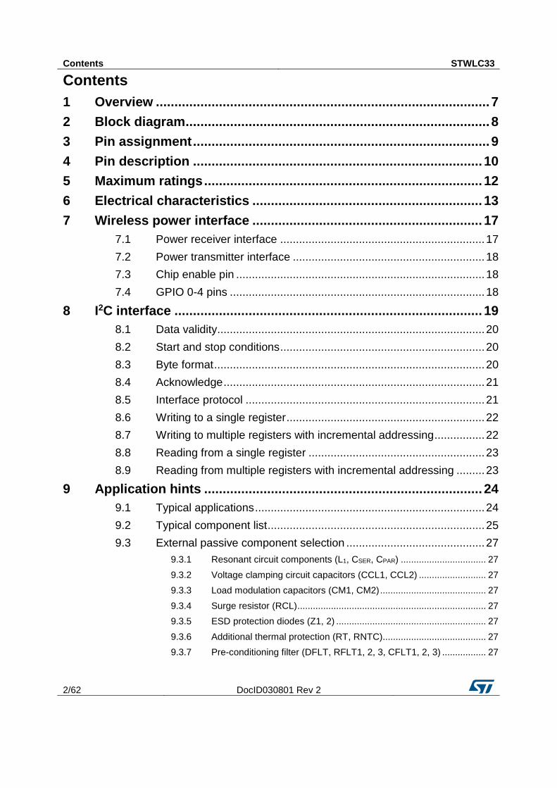
Contents
1 Overview .......................................................................................... 7
2 Block diagram .................................................................................. 8
3 Pin assignment ................................................................................ 9
4 Pin description .............................................................................. 10
5 Maximum ratings ........................................................................... 12
6 Electrical characteristics .............................................................. 13
7 Wireless power interface .............................................................. 17
7.1 Power receiver interface ................................................................. 17
7.2 Power transmitter interface ............................................................. 18
7.3 Chip enable pin ............................................................................... 18
7.4 GPIO 0-4 pins ................................................................................. 18
8 I2C interface ................................................................................... 19
8.1 Data validity..................................................................................... 20
8.2 Start and stop conditions ................................................................. 20
8.3 Byte format ...................................................................................... 20
8.4 Acknowledge ................................................................................... 21
8.5 Interface protocol ............................................................................ 21
8.6 Writing to a single register ............................................................... 22
8.7 Writing to multiple registers with incremental addressing ................ 22
8.8 Reading from a single register ........................................................ 23
8.9 Reading from multiple registers with incremental addressing ......... 23
9 Application hints ........................................................................... 24
9.1 Typical applications ......................................................................... 24
9.2 Typical component list ..................................................................... 25
9.3 External passive component selection ............................................ 27
9.3.1 Resonant circuit components (L1, CSER, CPAR) ................................. 27
9.3.2 Voltage clamping circuit capacitors (CCL1, CCL2) .......................... 27
9.3.3 Load modulation capacitors (CM1, CM2) ......................................... 27
9.3.4 Surge resistor (RCL) ......................................................................... 27
9.3.5 ESD protection diodes (Z1, 2) .......................................................... 27
9.3.6 Additional thermal protection (RT, RNTC)........................................ 27
9.3.7 Pre-conditioning filter (DFLT, RFLT1, 2, 3, CFLT1, 2, 3) ................. 27

STWLC33 Contents
DocID030801 Rev 2 3/62
10 PCB routing strategy and component placement ....................... 28
11 Examples of system integration ................................................... 29
11.1 Standalone application (Rx mode only) ........................................... 29
11.2 Small pin count (TRx mode capable) .............................................. 29
11.3 Maximum features (TRx mode capable) ......................................... 30
12 NVM configuration update procedure .......................................... 31
12.1 Read NVM sector procedure ........................................................... 31
12.2 Write NVM sector procedure ........................................................... 31
13 Procedure to load executable binary ........................................... 32
14 I2C register map description ......................................................... 33
14.1 Overview ......................................................................................... 33
15 NVM map description .................................................................... 52
16 Package information ..................................................................... 58
16.1 Flip Chip 52 bumps (3.97x2.67 mm) package information .............. 58
17 Reference ....................................................................................... 60
18 Revision history ............................................................................ 61

List of tables STWLC33
4/62 DocID030801 Rev 2
List of tables
Table 1: Device summary ........................................................................................................................... 1 Table 2: Pin description ............................................................................................................................ 10 Table 3: Absolute maximum ratings ......................................................................................................... 12 Table 4: Thermal data ............................................................................................................................... 12 Table 5: STWLC33 electrical characteristics ............................................................................................ 13 Table 6: Typical component list for Rx operation only .............................................................................. 25 Table 7: Typical component list for TRx operation ................................................................................... 26 Table 8: Packet structure to load executable binary ................................................................................. 32 Table 9: Register overview ....................................................................................................................... 33 Table 10: Chip_ID register ........................................................................................................................ 34 Table 11: Chip_Rev register ..................................................................................................................... 36 Table 12: FW_Major_Rev register ............................................................................................................ 36 Table 13: FW_Minor_Rev register ............................................................................................................ 37 Table 14: Status_Rx register .................................................................................................................... 37 Table 15: INT_Rx register ......................................................................................................................... 37 Table 16: INT_Enable_Rx register ........................................................................................................... 38 Table 17: INT_Clear_Rx register .............................................................................................................. 38 Table 18: EPT register .............................................................................................................................. 38 Table 19: VOUT_Set register ................................................................................................................... 39 Table 20: IOUT_L register ........................................................................................................................ 39 Table 21: IOUT_H register ........................................................................................................................ 39 Table 22: Die_Temp_L register ................................................................................................................ 39 Table 23: Die_Temp_H register ................................................................................................................ 39 Table 24: ILim_Set register ....................................................................................................................... 40 Table 25: Sys_Op_Mode register ............................................................................................................. 40 Table 26: Com register ............................................................................................................................. 40 Table 27: FWSwitchKey register .............................................................................................................. 41 Table 28: Qi_Data_Send register ............................................................................................................. 41 Table 29: RXID register ............................................................................................................................ 41 Table 30: OVP_Set register ...................................................................................................................... 42 Table 31: VRECT_L register ..................................................................................................................... 42 Table 32: VRECT_H register .................................................................................................................... 42 Table 33: VOUT_L register ....................................................................................................................... 42 Table 34: VOUT_H register ...................................................................................................................... 42 Table 35: PMA_ADV_L register ................................................................................................................ 43 Table 36: PMA_ADV_H register ............................................................................................................... 43 Table 37: Op_Freq_L register ................................................................................................................... 43 Table 38: Op_Freq_H register .................................................................................................................. 43 Table 39: Ping_Freq_L register ................................................................................................................ 43 Table 40: Ping_Freq_H register ................................................................................................................ 44 Table 41: PRMC_ID_L register ................................................................................................................. 44 Table 42: PRMC_ID_H register ................................................................................................................ 44 Table 43: Qi_Data_Send_Control register ............................................................................................... 44 Table 44: NVM_Control register ............................................................................................................... 45 Table 45: NVM_Manipulation register ...................................................................................................... 45 Table 46: Qi_Data_Rcvd_Status register ................................................................................................. 45 Table 47: Qi_Data_Rcvd_Length register ................................................................................................ 45 Table 48: Qi_Data_Rcvd_Format register ................................................................................................ 46 Table 49: Qi_Data_Rcvd register ............................................................................................................. 46 Table 50: Qi_Power_Transfer_Contract register ...................................................................................... 46 Table 51: Max_Freq_Tx_L register ........................................................................................................... 46 Table 52: Max_Freq_Tx_H register .......................................................................................................... 47 Table 53: Min_Freq_Tx_L register ............................................................................................................ 47

STWLC33 List of tables
DocID030801 Rev 2 5/62
Table 54: Min_Freq_Tx_H register ........................................................................................................... 47 Table 55: Ping_Freq_Tx_L register .......................................................................................................... 47 Table 56: Ping_Freq_Tx_H register .......................................................................................................... 47 Table 57: ASK_High_Thr_Tx register ....................................................................................................... 48 Table 58: ASK_Low_Thr_Tx register ........................................................................................................ 48 Table 59: RxPower_Rcvd_Value_Tx register ........................................................................................... 48 Table 60: EPT_Reason_Tx register ......................................................................................................... 48 Table 61: Status_Tx register ..................................................................................................................... 49 Table 62: INT_Tx register ......................................................................................................................... 49 Table 63: INT_Enable_Tx register ............................................................................................................ 49 Table 64: VRECT_Tx_L register ............................................................................................................... 50 Table 65: VRECT_Tx_H register .............................................................................................................. 50 Table 66: IIN_Tx_L register ...................................................................................................................... 50 Table 67: IIN_Tx_H register ...................................................................................................................... 50 Table 68: INT_Clear_Tx register .............................................................................................................. 50 Table 69: NVM organization ..................................................................................................................... 52 Table 70: Sector 0: Qi LP profile configuration ......................................................................................... 52 Table 71: Sector 1: Qi MP profile configuration ........................................................................................ 53 Table 72: Sector 2: Qi general configuration ............................................................................................ 54 Table 73: Sector 3: Qi identification .......................................................................................................... 54 Table 74: Sector 4: PMA LP profile configuration ..................................................................................... 55 Table 75: Sector 6: PMA general configuration ........................................................................................ 56 Table 76: Sector 7: PMA identification ...................................................................................................... 56 Table 77: Sector 8: Platform configuration ............................................................................................... 57 Table 78: Flip Chip (3.97x2.67 mm) package mechanical data ............................................................... 59 Table 79: Document revision history ........................................................................................................ 61

List of figures STWLC33
6/62 DocID030801 Rev 2
List of figures
Figure 1: STWLC33 block diagram ............................................................................................................. 8 Figure 2: Pinout top view ............................................................................................................................ 9 Figure 3: Init flowchart............................................................................................................................... 17 Figure 4: I2C timing reference ................................................................................................................... 19 Figure 5: Data validity on the I2C bus ....................................................................................................... 20 Figure 6: Start and stop condition on the I2C bus .................................................................................... 20 Figure 7: Bit transfer ................................................................................................................................. 21 Figure 8: Acknowledge on the I2C bus ..................................................................................................... 21 Figure 9: Interface protocol ....................................................................................................................... 22 Figure 10: Writing to a single register ....................................................................................................... 22 Figure 11: Writing to multiple registers ..................................................................................................... 22 Figure 12: Reading from a single register................................................................................................. 23 Figure 13: Reading from multiple registers ............................................................................................... 23 Figure 14: STWLC33 schematic diagram for Rx operation only .............................................................. 24 Figure 15: STWLC33 schematic diagram for TRx operation .................................................................... 25 Figure 16: System integration example 1 ................................................................................................. 29 Figure 17: System integration example 2 ................................................................................................. 30 Figure 18: System integration example 3 ................................................................................................. 30 Figure 19: Flip Chip (3.97x2.67 mm) package outline .............................................................................. 58 Figure 20: Flip Chip (3.97x2.67 mm) recommended footprint .................................................................. 59

STWLC33 Overview
DocID030801 Rev 2 7/62
1 Overview
The STWLC33 is first of all a wireless power receiver providing regulated voltage to the output. The power receiver firmware is placed in ROM and is able to operate fully autonomously. Optionally, the device can be controlled and configured over I2C interface. The device contains several output pins, for example to drive signal LEDs or to indicate the status to the host processor. The STWLC33 contains also hardware blocks to support transmitter mode functions. The transmitter firmware is not placed inside, but has to be loaded over I2C into internal RAM. In this manner, the device can serve as a wireless power transmitter with limited functions. The same coil can be used (with limitations coming from the different coil parameters) or an external switch can be used to connect Tx mode coil.

Block diagram STWLC33
8/62 DocID030801 Rev 2
2 Block diagram Figure 1: STWLC33 block diagram

STWLC33 Pin assignment
DocID030801 Rev 2 9/62
3 Pin assignment Figure 2: Pinout top view
Pin description STWLC33
10/62 DocID030801 Rev 2
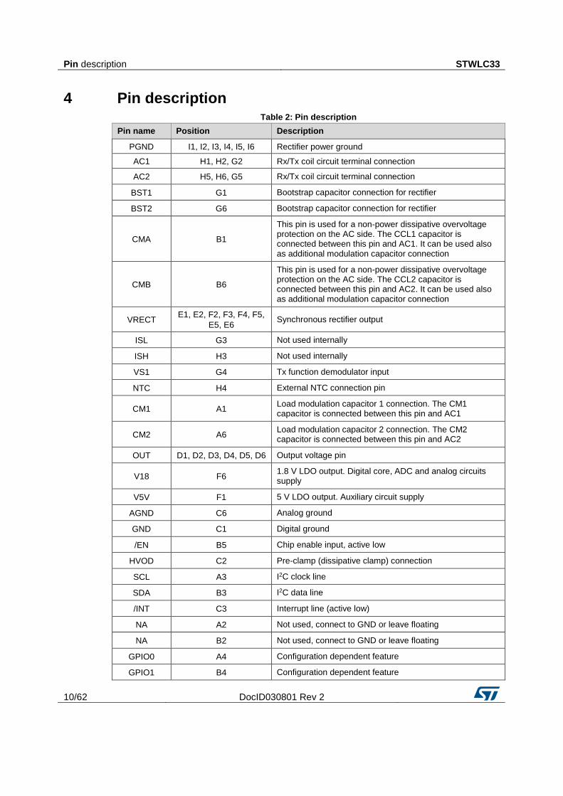
4 Pin description Table 2: Pin description
Pin name Position Description
PGND I1, I2, I3, I4, I5, I6 Rectifier power ground
AC1 H1, H2, G2 Rx/Tx coil circuit terminal connection
AC2 H5, H6, G5 Rx/Tx coil circuit terminal connection
BST1 G1 Bootstrap capacitor connection for rectifier
BST2 G6 Bootstrap capacitor connection for rectifier
CMA B1
This pin is used for a non-power dissipative overvoltage protection on the AC side. The CCL1 capacitor is connected between this pin and AC1. It can be used also as additional modulation capacitor connection
CMB B6
This pin is used for a non-power dissipative overvoltage protection on the AC side. The CCL2 capacitor is connected between this pin and AC2. It can be used also as additional modulation capacitor connection
VRECT E1, E2, F2, F3, F4, F5,
E5, E6 Synchronous rectifier output
ISL G3 Not used internally
ISH H3 Not used internally
VS1 G4 Tx function demodulator input
NTC H4 External NTC connection pin
CM1 A1 Load modulation capacitor 1 connection. The CM1 capacitor is connected between this pin and AC1
CM2 A6 Load modulation capacitor 2 connection. The CM2 capacitor is connected between this pin and AC2
OUT D1, D2, D3, D4, D5, D6 Output voltage pin
V18 F6 1.8 V LDO output. Digital core, ADC and analog circuits supply
V5V F1 5 V LDO output. Auxiliary circuit supply
AGND C6 Analog ground
GND C1 Digital ground
/EN B5 Chip enable input, active low
HVOD C2 Pre-clamp (dissipative clamp) connection
SCL A3 I2C clock line
SDA B3 I2C data line
/INT C3 Interrupt line (active low)
NA A2 Not used, connect to GND or leave floating
NA B2 Not used, connect to GND or leave floating
GPIO0 A4 Configuration dependent feature
GPIO1 B4 Configuration dependent feature
STWLC33 Pin description
DocID030801 Rev 2 11/62
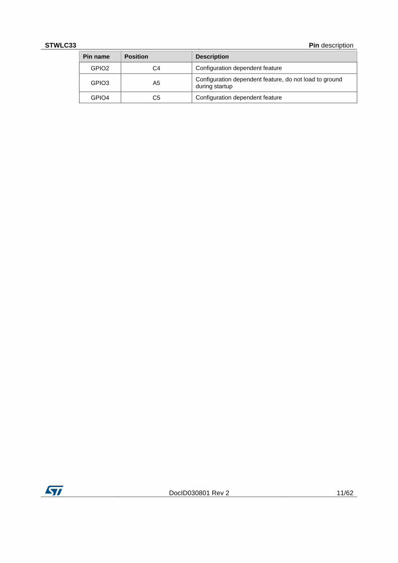
Pin name Position Description
GPIO2 C4 Configuration dependent feature
GPIO3 A5 Configuration dependent feature, do not load to ground during startup
GPIO4 C5 Configuration dependent feature
Maximum ratings STWLC33
12/62 DocID030801 Rev 2
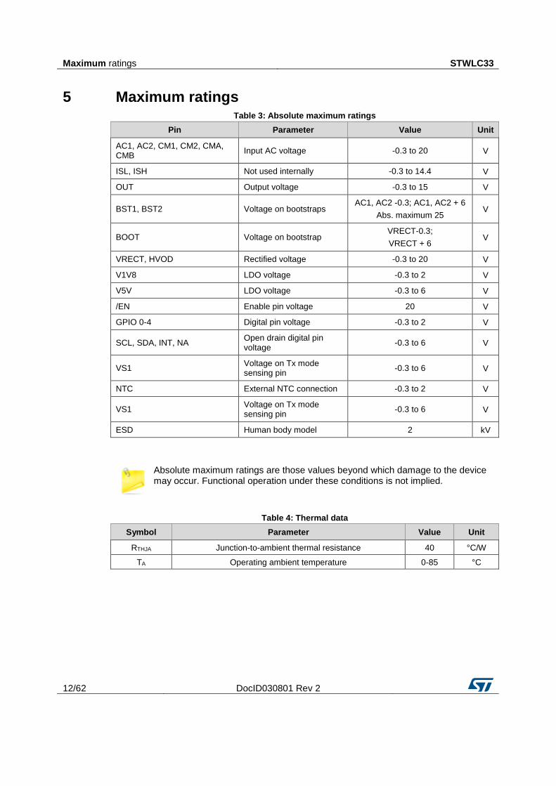
5 Maximum ratings Table 3: Absolute maximum ratings
Pin Parameter Value Unit
AC1, AC2, CM1, CM2, CMA, CMB
Input AC voltage -0.3 to 20 V
ISL, ISH Not used internally -0.3 to 14.4 V
OUT Output voltage -0.3 to 15 V
BST1, BST2 Voltage on bootstraps AC1, AC2 -0.3; AC1, AC2 + 6
Abs. maximum 25 V
BOOT Voltage on bootstrap VRECT-0.3;
VRECT + 6 V
VRECT, HVOD Rectified voltage -0.3 to 20 V
V1V8 LDO voltage -0.3 to 2 V
V5V LDO voltage -0.3 to 6 V
/EN Enable pin voltage 20 V
GPIO 0-4 Digital pin voltage -0.3 to 2 V
SCL, SDA, INT, NA Open drain digital pin voltage
-0.3 to 6 V
VS1 Voltage on Tx mode sensing pin
-0.3 to 6 V
NTC External NTC connection -0.3 to 2 V
VS1 Voltage on Tx mode sensing pin
-0.3 to 6 V
ESD Human body model 2 kV
Absolute maximum ratings are those values beyond which damage to the device may occur. Functional operation under these conditions is not implied.
Table 4: Thermal data
Symbol Parameter Value Unit
RTHJA Junction-to-ambient thermal resistance 40 °C/W
TA Operating ambient temperature 0-85 °C
STWLC33 Electrical characteristics
DocID030801 Rev 2 13/62
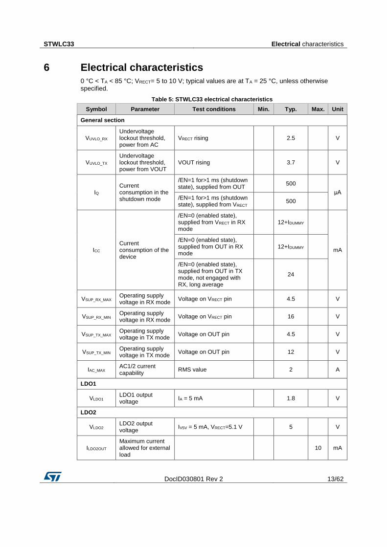
6 Electrical characteristics
0 °C < TA < 85 °C; VRECT= 5 to 10 V; typical values are at TA = 25 °C, unless otherwise specified.
Table 5: STWLC33 electrical characteristics
Symbol Parameter Test conditions Min. Typ. Max. Unit
General section
VUVLO_RX Undervoltage lockout threshold, power from AC
VRECT rising
2.5
V
VUVLO_TX Undervoltage lockout threshold, power from VOUT
VOUT rising
3.7
V
IQ Current consumption in the shutdown mode
/EN=1 for>1 ms (shutdown state), supplied from OUT
500
μA /EN=1 for>1 ms (shutdown state), supplied from VRECT
500
ICC Current consumption of the device
/EN=0 (enabled state), supplied from VRECT in RX mode
12+IDUMMY
mA
/EN=0 (enabled state), supplied from OUT in RX mode
12+IDUMMY
/EN=0 (enabled state), supplied from OUT in TX mode, not engaged with RX, long average
24
VSUP_RX_MAX Operating supply voltage in RX mode
Voltage on VRECT pin
4.5
V
VSUP_RX_MIN Operating supply voltage in RX mode
Voltage on VRECT pin
16
V
VSUP_TX_MAX Operating supply voltage in TX mode
Voltage on OUT pin
4.5
V
VSUP_TX_MIN Operating supply voltage in TX mode
Voltage on OUT pin
12
V
IAC_MAX AC1/2 current capability
RMS value
2
A
LDO1
VLDO1 LDO1 output voltage
IA = 5 mA
1.8
V
LDO2
VLDO2 LDO2 output voltage
IV5V = 5 mA, VRECT=5.1 V
5
V
ILDO2OUT Maximum current allowed for external load
10 mA

Electrical characteristics STWLC33
14/62 DocID030801 Rev 2
Symbol Parameter Test conditions Min. Typ. Max. Unit
Synchronous rectifier
Efficiency Target rectifier efficiency
IRECT=1 A, VRECT=5.2 V, fRECT=100 kHz to 250 kHz
97
% IRECT=1 A, VRECT=9.2 V, fRECT=100 kHz to 250 kHz
97
fRECTIFIER Rectifier frequency range
50
500 kHz
Inverter driver
fINV Inverter frequency range
100-300
kHz
AC clamp
VCLAMP AC clamp threshold
15
V
VCLAMP_HYST AC clamp hysteresis
0.5
V
ICLAMP AC clamp max. current
1.0
A
Pre-clamp (HVOD pin)
VHVOD VRECT voltage threshold
13.5
V
VHVOD_HYST VR voltage active clamp hysteresis
0.7
V
Load modulation
RDSONCM1,2 Load modulation MOS RDS(on)
VRECT = 5 V
1
Ω
ICMOD_MAX MOD1/2 current capability
RMS value
0.5
A
Dummy load
IDUMMY
Dummy load current
VRECT = 5 to 12 V
32
mA
Dummy load IOUT threshold
Enabled at IOUT < threshold
200
mA
Thermal protection
tSHDN Thermal shutdown
150
°C
tSHDN_HYST Thermal shutdown hysteresis
20
°C
Current sensor
IRANGE_VLD Sensing current range
RX mode 0
1600 mA
TX mode 1000
0
VOUT_VLD_TOL Overall block tolerance
1
%
IEOC End of charging current threshold
VOUT = 3.5 to 12.5 V
150
mA

STWLC33 Electrical characteristics
DocID030801 Rev 2 15/62
Symbol Parameter Test conditions Min. Typ. Max. Unit
Power LDO
VOUT Output voltage range
VOUT_SET=00h
3.5
V
VOUT_SET=5Ah
12.5
VOUT_STEP Programmable step size
VOUT_SET LSB size
0.1
V
VDROP LDO drop voltage IOUT=1 A
70
mV
VRECT_RANGE Typical input voltage range
VOUT = 5 V
5.1 – 8 V
VOUT = 9 V
9.1 – 12
LINEREG Line regulation IOUT = 0.1 A, VOUT = 5 V,
VRECT 5.1 V↔15 V 3 10 mV
LOADREG Load regulation VRECT=5.1 V, VOUT=5 V,
IOUT 1 mA↔1 A 30 70 mV
OVPVOUT Overvoltage protection threshold
VOUT+25%
V
IOVERCURR LDO overcurrent protection
Security HW protection
1700
mA
Current limitation loop
ILIM Input current limitation threshold
ILIM_SET=0Fh
1600 mA
ILIM_SET=00h
100
ILIM_STEP Programmable step size
ILIM_SET LSB size
100
mA
ILIM_TOL ILIM threshold tolerance
ILIM_SET=0Fh
5
%
ILIM_SET=01h
10
%
Digital interface (GPIO pins, EN, I2C, INT)
VIL Low level input voltage
0.55 V
VIH High level input voltage
1.14
V
VOH GPIOx high level output voltage
Output high, source=3 mA 1.25
V
IOH GPIOx pin current capability
Output high 3
mA
VOL Low level output voltage
Output low, sink = 3 mA
360
mV
Microcontroller
Architecture ARM Cortex
32
bit
RAM RAM size
8
kB
NVM Memory size for configuration
4
kbit
Clock generator

Electrical characteristics STWLC33
16/62 DocID030801 Rev 2
Symbol Parameter Test conditions Min. Typ. Max. Unit
fOSC Clock generator and PWM timer frequency
VSUP = VUVLO to 15 V
32
MHz
fOSC_TOL Tolerance of the clock generator frequency
T = 0 °C to 85 °C -4
+4 %

STWLC33 Wireless power interface
DocID030801 Rev 2 17/62
7 Wireless power interface
7.1 Power receiver interface
Power receiver is the default mode of operation.
Following protocols are supported:
Qi 1.2 including FOD extensions – up to 15 W (1.5 A @ 10 V)
Qi backward compatible basic power profile – up to 5 W (1.0 A @ 5 V)
PMA SR1 (AirFuel inductive) – up to 5 W (0.9 A @ 5.6 V)
The STWLC33 selects automatically between Qi mode and PMA mode based on Tx frequency measurement and PMA advertising detection. See figure below.
Figure 3: Init flowchart
In case of Qi mode the STWLC33 goes autonomously through Ping, identification, negotiation and calibration phase to power transfer phase. During power transfer phase, the STWLC33 sends periodically RxPower and control error packets. If overvoltage, overcurrent or overtemperature event happens, the STWLC33 sends automatically end power transfer packet.
During power transfer phase, the device can be commanded over I2C to send end power transfer packet (with any response value) or any custom packet (proprietary packets or e.g. charge status packet). The custom packet can be sent in any of three modes: without expecting a reply, expecting pattern response from Tx or expecting data packet response from Tx. If the response is received the content is captured and is available in I2C registers.
In case of PMA mode, the STWLC33 goes autonomously through Ping and identification phase to power transfer phase. If PMA advertising message is received the content is captured in I2C registers. If overvoltage, overcurrent or overtemperature event happens, the STWLC33 sends automatically end-of-charge signal.
In every operating mode the output voltage can be reconfigured over I2C on the fly or stored in NVM as the new default value.
Important notes:
Changing the output voltage must respect the overall system design (coil selection, transmitter types etc.)
Load must avoid fast transients
Minimum operating load is 150 mA (to ensure interoperability with all Tx)

Wireless power interface STWLC33
18/62 DocID030801 Rev 2
Starting load should not exceed 2.5 W, ramping to full power is recommended
7.2 Power transmitter interface
Power transmitter functions are available only after loading the STWLC33 TxMode RAM binary. See Section 13: "Procedure to load executable binary" for instructions.
The implemented protocol is based on Qi.
The maximum power delivered to the Rx is strongly influenced by coil selection. Using common thin Rx coils in Tx mode limits the delivered power to approximately 3 W (on Rx output).
7.3 Chip enable pin
Chip enable pin can block the operation of the device by putting the device in reset state. After releasing the reset, the STWLC33 starts always in Rx mode.
7.4 GPIO 0-4 pins
GPIO functions can be assigned in NVM. GPIO3 pin needs special care because it has connected an internal pull-up and must not be tied low during the device startup.

STWLC33 I2C interface
DocID030801 Rev 2 19/62
8 I2C interface
The STWLC33 can operate fully independently on I2C interface but when it is embedded into an application I2C can provide a flexibility to get the device status, executing custom commands or reconfiguring the default values. In parallel to I²C bus there is also the interrupt pin to indicate events.
The I²C bus™ is configured as a slave serial interface compatible with the I²C register, built with a data line (SDA) and a clock line (SCL):
SCL: input clock
SDA: input/output bidirectional data transfer line
The STWLC33 device works as a slave and supports the following data transfer mode: standard mode (100 kbit/s) and fast mode (400 kbit/s) as defined in the I2C_busTM specification version developed by Philips semiconductor.
The STWLC33 device supports 7-bit addressing, plus one bit dedicated to write (0) or read (1) mode. The master initiates data transfer by generating a start condition. The start condition is when a high to low transition occurs on SDA line while SCL is high. The master then generates the SCL pulses and transmits the 7-bit address for the device IDD plus 1 bit for read/write.
The device with a matching address only generates acknowledge by pulling the SDA line low during the entire period of the 9th SCL cycle. The SDA data are shifted MSB first. The master device sends 8 bits on SDA corresponding to the register address followed by acknowledge and 8-bit data field corresponding to the register content followed or not by another acknowledge. To signal the end of the data transfer, the master generates a STOP condition by pulling the SDA line from low to high while the SCL line is high. This releases the bus and stops the communication link with the addressed slave device.
Figure 4: I2C timing reference

I2C interface STWLC33
20/62 DocID030801 Rev 2
8.1 Data validity
As shown in Figure 5: "Data validity on the I2C bus", the data on the SDA line must be stable during the high period of the clock. The HIGH and LOW state of the data line can only change when the clock signal on the SCL line is LOW.
Figure 5: Data validity on the I2C bus
8.2 Start and stop conditions
Both DATA and CLOCK lines remain HIGH when the bus is not busy. As shown in figure below, a start condition is a HIGH to LOW transition of the SDA line while SCL is HIGH. The stop condition is a LOW to HIGH transition of the SDA line while SCL is HIGH. A STOP condition must be sent before each START condition.
Figure 6: Start and stop condition on the I2C bus
8.3 Byte format
Every byte transferred to the SDA line must contain 8 bits. Each byte must be followed by an acknowledge bit. The MSB is transferred first. One data bit is transferred during each clock pulse. The data on the SDA line must remain stable during the HIGH period of the clock pulse. Any change in the SDA line at this time is meant as a control signal.

STWLC33 I2C interface
DocID030801 Rev 2 21/62
Figure 7: Bit transfer
8.4 Acknowledge
The master (µC) puts a resistive HIGH level on the SDA line during the acknowledge clock pulse (see Figure 8: "Acknowledge on the I2C bus"). The peripheral (STWLC33), which acknowledges, has to pull down (LOW) the SDA line during the acknowledge clock pulse, so that the SDA line is stable LOW during this clock pulse. The peripheral, which has been addressed, has to generate an acknowledge pulse after the reception of each byte, otherwise the SDA line remains at the HIGH level during the 9th clock pulse duration. In this case, the master transmitter can generate the STOP information in order to abort the transfer. The STWLC33 does not generate acknowledge if the power supply is below the undervoltage lockout threshold.
Figure 8: Acknowledge on the I2C bus
8.5 Interface protocol
The interface protocol is composed of (see figure below):
A start condition (START)
A device address + R/W bit (read =1 / write =0)
A register H address byte
A register L address byte
A sequence of data n* (1 byte + acknowledge)
A stop condition (STOP)
The register address byte determines the first register in which the read or write operation takes place. When the read or write operation is finished, the register address is automatically incremented.

I2C interface STWLC33
22/62 DocID030801 Rev 2
Figure 9: Interface protocol
8.6 Writing to a single register
Writing to a single register starts with a START bit followed by the 7-bit device address of STWLC33. The 8th bit is the R/W bit, which is 0 in this case. R/W = 1 means a reading operation. Then the master waits for the STWLC33 acknowledge. Then the 8-bit address of register is sent to STWLC33. It is also followed by an acknowledge pulse. The last transmitted byte is the data that is going to be written to the register. It is again followed by an acknowledge pulse from the STWLC33. The master then generates a STOP bit and the communication is over. See Figure 10: "Writing to a single register" below.
Figure 10: Writing to a single register
8.7 Writing to multiple registers with incremental addressing
The STWLC33 supports writing to multiple registers with incremental addressing. When data is written to register, the address register is automatically incremented, so the next data can be sent without sending the device address and the register address again. See Figure 11: "Writing to multiple registers".
Figure 11: Writing to multiple registers

STWLC33 I2C interface
DocID030801 Rev 2 23/62
8.8 Reading from a single register
The reading operation starts with a START bit followed by 7-bit device address of the STWLC33. The 8th bit is the R/W bit, which is 0 in this case. The STWLC33 confirms to receive the address + R/W bit by an acknowledge pulse. The address of the register, which should be read, is sent afterward and confirmed again by an acknowledge pulse of the STWLC33 again. The master generates a START bit again and sends the device address followed by the R/W bit, which is 1 now. The STWLC33 confirms to receive the address + R/W bit by an acknowledge pulse and starts to send the data to the master. No acknowledge pulse from the master is required after receiving the data. Then the master generates a STOP bit to terminate the communication.
Figure 12: Reading from a single register
8.9 Reading from multiple registers with incremental addressing
Reading from multiple registers starts in the same way like reading from a single register. As soon as the first register is read, the register address is automatically incremented. If the master generates an acknowledge pulse after receiving the data from the first register, then the reading of the next register can start immediately without sending the device address and the register address again. The last acknowledge pulse before the STOP bit is not required. See Figure 13: "Reading from multiple registers".
Figure 13: Reading from multiple registers
Application hints STWLC33
24/62 DocID030801 Rev 2
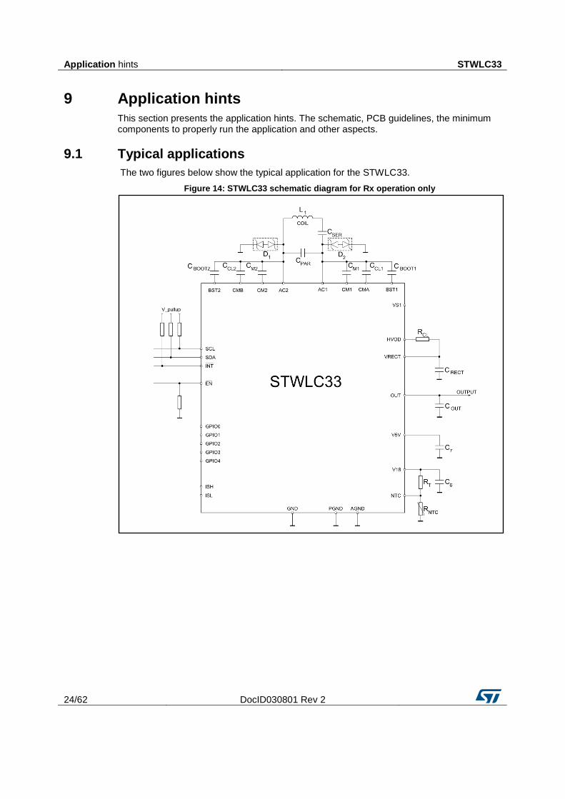
9 Application hints
This section presents the application hints. The schematic, PCB guidelines, the minimum components to properly run the application and other aspects.
9.1 Typical applications
The two figures below show the typical application for the STWLC33.
Figure 14: STWLC33 schematic diagram for Rx operation only
STWLC33 Application hints
DocID030801 Rev 2 25/62
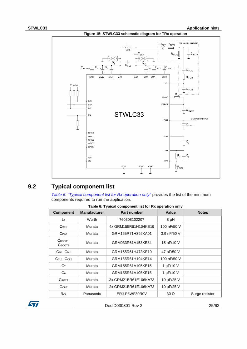
Figure 15: STWLC33 schematic diagram for TRx operation
9.2 Typical component list
Table 6: "Typical component list for Rx operation only" provides the list of the minimum components required to run the application.
Table 6: Typical component list for Rx operation only
Component Manufacturer Part number Value Notes
L1 Wurth 760308102207 8 µH
CSER Murata 4x GRM155R61H104KE19 100 nF/50 V
CPAR Murata GRM155R71H392KA01 3.9 nF/50 V
CBOOT1, CBOOT2
Murata GRM033R61A153KE84 15 nF/10 V
CM1, CM2 Murata GRM155R61H473KE19 47 nF/50 V
CCL1, CCL2 Murata GRM155R61H104KE14 100 nF/50 V
C7 Murata GRM155R61A105KE15 1 µF/10 V
C6 Murata GRM155R61A105KE15 1 µF/10 V
CRECT Murata 3x GRM21BR61E106KA73 10 µF/25 V
COUT Murata 2x GRM21BR61E106KA73 10 µF/25 V
RCL Panasonic ERJ-P6WF30R0V 30 Ω Surge resistor

Application hints STWLC33
26/62 DocID030801 Rev 2
Component Manufacturer Part number Value Notes
D1,2 NXP PESD12VV1BL
ESD protection diodes
RT
30 kΩ Optional
RNTC
100 kΩ Optional
All the above components refer to a typical application. Operation of the device is not limited to the choice of these external components.
Table 7: Typical component list for TRx operation
Component Manufacturer Part number Value Notes
L1 Wurth 760308102207 8 µH
CSER Murata 4x GRM155R61H104KE19 100 nF/50 V
CPAR Murata GRM155R71H392KA01 3.9 nF/50 V
CBOOT1, CBOOT2
Murata GRM033R61A153KE84 15 nF/10 V
CM1, CM2 Murata GRM155R61H473KE19 47 nF/50 V
CCL1, CCL2 Murata GRM155R61H104KE14 100 nF/50 V
C7 Murata GRM155R61A105KE15 1µF/10V
C6 Murata GRM155R61A105KE15 1 µF/10 V
CRECT Murata 3x GRM21BR61E106KA73 10 µF/25 V
COUT Murata 2x GRM21BR61E106KA73 10 µF/25 V
RCL Panasonic ERJ-P6WF30R0V 30 Ω Surge resistor
D1,2 NXP PESD12VV1BL
ESD protection diodes
DFLT ST BAT48
Schottky diode
RFLT1
10 kΩ/1%
RFLT2
68 kΩ/1%
RFLT3
620 Ω/1%
CFLT1 Murata GRM155R71H152KA01 1.5 nF/50 V
CFLT2 Murata GRM155R71H223KA12 22 nF/50 V
CFLT3 Murata GRM155R71H682KA88 6.8 nF/50 V
RT
30 kΩ Optional
RNTC
100 kΩ Optional
All the above components refer to a typical application. Operation of the device is not limited to the choice of these external components.

STWLC33 Application hints
DocID030801 Rev 2 27/62
9.3 External passive component selection
9.3.1 Resonant circuit components (L1, CSER, CPAR)
Rx coil should be selected with respect to the requested transferred power. The inductance of the L 1 coil and capacitance of CSER and CPAR capacitors define the resonant frequency of the LC circuit. This frequency should fit the requests given by the wireless power transfer standards.
9.3.2 Voltage clamping circuit capacitors (CCL1, CCL2)
The X5R type is suitable for this purpose. The value of the caps should move the resonant frequency of the circuit enough in overvoltage conditions to ensure the VRECT voltage decreases fast.
9.3.3 Load modulation capacitors (CM1, CM2)
The X5R type is suitable for this purpose.
9.3.4 Surge resistor (RCL)
The surge resistor (pulse withstanding resistor) is recommended to protect the device from voltage peaks coming from coil. It needs to dissipate VRECT voltage peaks above HVOD protection threshold. A 0.5 W capable component is recommended.
9.3.5 ESD protection diodes (Z1, 2)
Using ESD diodes is recommended to protect the power input pins from fast voltage peaks coming from the coil. Diodes should have a high clamping threshold so not to open during normal operations (with respect to the selected VOUT plus the regulation headroom and positive modulation pulses).
9.3.6 Additional thermal protection (RT, RNTC)
This is an optional thermal protection that can sense the temperature directly at the desired spot, for example near the coil. The voltage threshold is configurable in NVM. The factory default value is 0, this means that the protection is off and NTC pin can be left unconnected. To enable the protection, non-zero value needs to be set in NVM. See NVM map and NVM update procedure.
9.3.7 Pre-conditioning filter (DFLT, RFLT1, 2, 3, CFLT1, 2, 3)
The filter is needed in Tx mode only for ASK demodulation. The purpose of the filter is to suppress the carrier frequency and provide envelope voltage to the VS1 pin. The voltage has to be within an operating range of VS1 pin 0 – 1.5 V and should also correspond with ASK threshold I2C register setting.

PCB routing strategy and component placement STWLC33
28/62 DocID030801 Rev 2
10 PCB routing strategy and component placement
Rules to be followed:
1. Auxiliary LDO capacitors C6 and C7 should be placed as close as possible to the STWLC33. Tracks connection should be short and placed to top layer. Capacitor ground can be connected directly into GND plane.
2. CRECT and COUT capacitors should be placed close to the STWLC33 with higher priority than RCL resistor or Tx mode filter.
3. Power tracks (AC1, AC2, VRECT and VOUT) should be routed wide enough with respect to high current that flows through.
4. AC1 and AC2 tracks should be routed close together to minimize the loop area.

STWLC33 Examples of system integration
DocID030801 Rev 2 29/62
11 Examples of system integration
11.1 Standalone application (Rx mode only)
This example shows the integration where only output power line is connected into the system. In this example, the STWLC33 operates fully autonomously. Tx mode is not available because it requires I2C connection.
Figure 16: System integration example 1
11.2 Small pin count (TRx mode capable)
This example shows how minimal integration can help to achieve a lot of functions.

Examples of system integration STWLC33
30/62 DocID030801 Rev 2
Figure 17: System integration example 2
11.3 Maximum features (TRx mode capable)
This example gives the chance of disabling the STWLC33 by host application processor. It also simplifies read power transfer status and low power / medium power status just by GPIO pin levels.
Figure 18: System integration example 3

STWLC33 NVM configuration update procedure
DocID030801 Rev 2 31/62
12 NVM configuration update procedure
NVM is organized into 16 sectors by 32 bytes. The read and write operations are defined for the whole sector, so it is not possible to read or write just a part of the sector.
To update a single byte in the sector: read the whole sector, update the byte and write back the whole sector.
For the NVM map the relevant section.
The device is power supplied either from wireless power or by providing 5 V to OUT pin.
It is important to note that: some reserved sectors contain factory calibration values. Modification to these values may result in unrecoverable loss of functionality.
12.1 Read NVM sector procedure
1. Write into register 8Fh (NVM_Control) a value that consists of NVM_R ORed with NVM_sector number.
2. Await for till NVM_R bit is cleared or 250 μs. 3. Read the data from registers 90h to AFh.
12.2 Write NVM sector procedure
1. Check if, in register 8Fh (NVM_Control), NVM_R and NVM_W bits are zero or simply await for 250 μs.
2. Prepare the data into registers 90h to AFh (or update the data after previous read). 3. Write into register 8Fh (NVM_Control) a value that consists of NVM_W ORed with
NVM_sector number.

Procedure to load executable binary STWLC33
32/62 DocID030801 Rev 2
13 Procedure to load executable binary
Loading the executable binary file into RAM over I²C interface consists of several steps.
1. Applying a power supply 2. Activation of the loader 3. Loading the binary data into RAM 4. Running the code from RAM
Power supply 5 V has to be provided to OUT pin.
First, write the password 0x5A to the FWSwitchKey register at address 0x4F.
Await for 250 µs or more and write data 0x40 to the com register at address 0x4E.
Await for 250 µs or more and write data 0x00 to address 0x00. It is a dummy write that activates the loader. This dummy write is not acknowledged by the STWLC33.
Await for 250 µs or more and then start to load the binary executable content.
It is recommended to send the binary executable data to packets of 128 bytes. However, shorter packets can be used (down to 4 bytes), but they increase the loading time.
The binary file size must be always a multiple of 4 bytes. Trailing zero can be added.
Table 8: "Packet structure to load executable binary" shows the packet structure for loading the binary.
Table 8: Packet structure to load executable binary
Byte index Byte/data Note
1 0xC2 Device address + R/W bit
2 Address of the first byte of the packet MSB Number of bytes already sent MSB
3 Address of the first byte of the packet MSB Number of bytes already sent LSB
4 First byte of the packet
5 Second byte of the packet
…
Packet size +2 (n-1)th byte of the packet
Packet size +3 nth byte of the packet
Await for 250 µs or more and write data 0x01 to address 0x00. This command terminates the binary file transfer.
Await for 250 µs or more and write data 0x5A to the FWSwitchKey register at address 0x4F.
Await for 250 µs or more and write data 0x40 to the Com register at address 0x4E.
Before starting the binary file loading process, the host has to check that the STWLC33 is not in power transfer with a wireless power transmitter.
STWLC33 I2C register map description
DocID030801 Rev 2 33/62
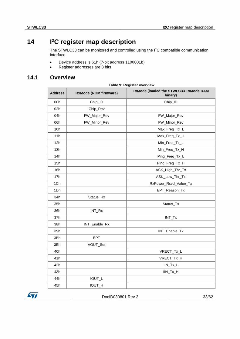
14 I2C register map description
The STWLC33 can be monitored and controlled using the I2C compatible communication interface.
Device address is 61h (7-bit address 1100001b)
Register addresses are 8 bits
14.1 Overview
Table 9: Register overview
Address RxMode (ROM firmware) TxMode (loaded the STWLC33 TxMode RAM
binary)
00h Chip_ID Chip_ID
02h Chip_Rev
04h FW_Major_Rev FW_Major_Rev
06h FW_Minor_Rev FW_Minor_Rev
10h
Max_Freq_Tx_L
11h
Max_Freq_Tx_H
12h
Min_Freq_Tx_L
13h
Min_Freq_Tx_H
14h
Ping_Freq_Tx_L
15h
Ping_Freq_Tx_H
16h
ASK_High_Thr_Tx
17h
ASK_Low_Thr_Tx
1Ch
RxPower_Rcvd_Value_Tx
1Dh
EPT_Reason_Tx
34h Status_Rx
35h
Status_Tx
36h INT_Rx
37h
INT_Tx
38h INT_Enable_Rx
39h
INT_Enable_Tx
3Bh EPT
3Eh VOUT_Set
40h
VRECT_Tx_L
41h
VRECT_Tx_H
42h
IIN_Tx_L
43h
IIN_Tx_H
44h IOUT_L
45h IOUT_H
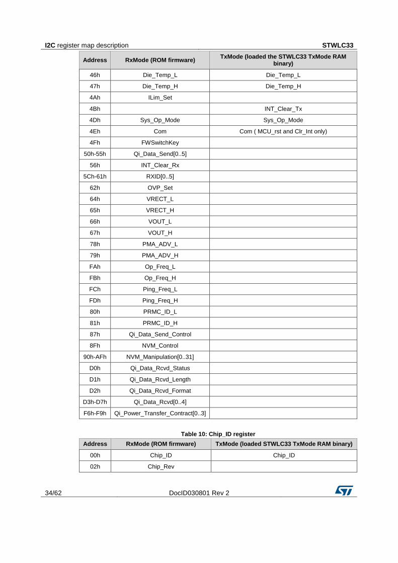
I2C register map description STWLC33
34/62 DocID030801 Rev 2
Address RxMode (ROM firmware) TxMode (loaded the STWLC33 TxMode RAM
binary)
46h Die_Temp_L Die_Temp_L
47h Die_Temp_H Die_Temp_H
4Ah ILim_Set
4Bh
INT_Clear_Tx
4Dh Sys_Op_Mode Sys_Op_Mode
4Eh Com Com ( MCU_rst and Clr_Int only)
4Fh FWSwitchKey
50h-55h Qi_Data_Send[0..5]
56h INT_Clear_Rx
5Ch-61h RXID[0..5]
62h OVP_Set
64h VRECT_L
65h VRECT_H
66h VOUT_L
67h VOUT_H
78h PMA_ADV_L
79h PMA_ADV_H
FAh Op_Freq_L
FBh Op_Freq_H
FCh Ping_Freq_L
FDh Ping_Freq_H
80h PRMC_ID_L
81h PRMC_ID_H
87h Qi_Data_Send_Control
8Fh NVM_Control
90h-AFh NVM_Manipulation[0..31]
D0h Qi_Data_Rcvd_Status
D1h Qi_Data_Rcvd_Length
D2h Qi_Data_Rcvd_Format
D3h-D7h Qi_Data_Rcvd[0..4]
F6h-F9h Qi_Power_Transfer_Contract[0..3]
Table 10: Chip_ID register
Address RxMode (ROM firmware) TxMode (loaded STWLC33 TxMode RAM binary)
00h Chip_ID Chip_ID
02h Chip_Rev

STWLC33 I2C register map description
DocID030801 Rev 2 35/62
Address RxMode (ROM firmware) TxMode (loaded STWLC33 TxMode RAM binary)
04h FW_Major_Rev FW_Major_Rev
06h FW_Minor_Rev FW_Minor_Rev
10h
Max_Freq_Tx_L
11h
Max_Freq_Tx_H
12h
Min_Freq_Tx_L
13h
Min_Freq_Tx_H
14h
Ping_Freq_Tx_L
15h
Ping_Freq_Tx_H
16h
ASK_High_Thr_Tx
17h
ASK_Low_Thr_Tx
1Ch
RxPower_Rcvd_Value_Tx
1Dh
EPT_Reason_Tx
34h Status_Rx
35h
Status_Tx
36h INT_Rx
37h
INT_Tx
38h INT_Enable_Rx
39h
INT_Enable_Tx
3Bh EPT
3Eh VOUT_Set
40h
VRECT_Tx_L
41h
VRECT_Tx_H
42h
IIN_Tx_L
43h
IIN_Tx_H
44h IOUT_L
45h IOUT_H
46h Die_Temp_L Die_Temp_L
47h Die_Temp_H Die_Temp_H
4Ah ILim_Set
4Bh
INT_Clear_Tx
4Dh Sys_Op_Mode Sys_Op_Mode
4Eh Com Com (only MCU_rst and Clr_Int)
4Fh FWSwitchKey
50h-55h Qi_Data_Send[0..5]
56h INT_Clear_Rx
5Ch-61h RXID[0..5]
62h OVP_Set

I2C register map description STWLC33
36/62 DocID030801 Rev 2
Address RxMode (ROM firmware) TxMode (loaded STWLC33 TxMode RAM binary)
64h VRECT_L
65h VRECT_H
66h VOUT_L
67h VOUT_H
78h PMA_ADV_L
79h PMA_ADV_H
FAh Op_Freq_L
FBh Op_Freq_H
FCh Ping_Freq_L
FDh Ping_Freq_H
80h PRMC_ID_L
81h PRMC_ID_H
87h Qi_Data_Send_Control
8Fh NVM_Control
90h-AFh NVM_Manipulation[0..31]
D0h Qi_Data_Rcvd_Status
D1h Qi_Data_Rcvd_Length
D2h Qi_Data_Rcvd_Format
D3h-D7h Qi_Data_Rcvd[0..4]
F6h-F9h Qi_Power_Transfer_Contract[0..3]
Chip_ID: chip unique ID byte
Table 11: Chip_Rev register
Bit 7 Bit 6 Bit 5 Bit 4 Bit 3 Bit 2 Bit 1 Bit 0
Addr = 02h Chip_Rev
POR = 01h 0 0 0 0 0 0 0 1
Comments Read-only Read-only
Chip_Rev: chip revision number
Table 12: FW_Major_Rev register
Bit 7 Bit 6 Bit 5 Bit 4 Bit 3 Bit 2 Bit 1 Bit 0
Addr = 04h FW_Major_Rev
POR = 00h 0 0 0 0 0 0 0 0
Comments Read-only
FW_Major_Rev: ROM / RAM memory firmware major revision number (check Sys_Op_Mode register to determine ROM/RAM)

STWLC33 I2C register map description
DocID030801 Rev 2 37/62
Table 13: FW_Minor_Rev register
Bit 7 Bit 6 Bit 5 Bit 4 Bit 3 Bit 2 Bit 1 Bit 0
Addr = 06h FW_Minor_Rev
POR = 00h 0 0 0 0 0 0 0 0
Comments Read-only
FW_Minor_Rev: ROM / RAM memory firmware minor revision number (check Sys_Op_Mode register to determine ROM/RAM)
Table 14: Status_Rx register
Bit 7 Bit 6 Bit 5 Bit 4 Bit 3 Bit 2 Bit 1 Bit 0
Addr = 34h Vout Vrect AC_Mis TX_Rcvd Reserved RX_OTP RX_OVP RX_OCP
POR = 20h 0 0 1 0 0 0 0 0
Comments R R R R R R R R
Vout: power output status; 0 = VOUT is below UVLO; 1 = VOUT is above UVLO
Vrect: VRECT status; 0 = VRECT is below UVLO; 1 = VRECT is above UVLO
AC_Mis: coil AC signal presence status; 0 = AC signal present in Rx mode; 1 = AC signal not present or Tx mode
TX_Rcvd: Tx data received (Rx mode only); 0 = no data received; 1 = data received
RX_OTP: Rx mode over temperature protection status; 0 = normal conditions; 1 = overtemperature
RX_OVP: Rx mode overvoltage protection status; 0 = normal conditions; 1 = overvoltage
RX_OCP: Rx mode overcurrent protection status; 0 = normal conditions; 1 = overcurrent
Table 15: INT_Rx register
Bit 7 Bit 6 Bit 5 Bit 4 Bit 3 Bit 2 Bit 1 Bit 0
Addr = 36h Vout Vrect AC_Mis TX_Rcvd Reserved RX_OTP RX_OVP RX_OCP
POR = 00h 0 0 0 0 0 0 0 0
Comments R R R R R R R R
Vout: 1 indicates pending interrupt (sensitive to any status change)
Vrect: 1 indicates pending interrupt (sensitive to any status change)
AC_Mis: 1 indicates pending interrupt (sensitive to any status change)
TX_Rcvd: 1 indicates pending interrupt
RX_OTP: 1 indicates pending interrupt
RX_OVP: 1 indicates pending interrupt
RX_OCP: 1 indicates pending interrupt

I2C register map description STWLC33
38/62 DocID030801 Rev 2
Table 16: INT_Enable_Rx register
Bit 7 Bit 6 Bit 5 Bit 4 Bit 3 Bit 2 Bit 1 Bit 0
Addr = 38h Vout Vrect AC_Mis TX_Rcvd Reserved RX_OTP RX_OVP RX_OCP
POR = 20h 0 0 1 0 0 0 0 0
Comments RW RW RW RW R RW RW
Vout: 0 INT pin output disabled; 1 = INT pin output enabled
Vrect: 0 INT pin output disabled; 1 = INT pin output enabled
AC_Mis: 0 INT pin output disabled; 1 = INT pin output enabled
TX_Rcvd: 0 INT pin output disabled; 1 = INT pin output enabled
RX_OTP: 0 INT pin output disabled; 1 = INT pin output enabled
RX_OVP: 0 INT pin output disabled; 1 = INT pin output enabled
RX_OCP: 0 INT pin output disabled; 1 = INT pin output enabled
Note: POR values are the default values after the STWLC33 powers up. Wireless standard detection value is automatically overwritten by NVM pre-configured value for the related wireless standard.
Table 17: INT_Clear_Rx register
Bit 7 Bit 6 Bit 5 Bit 4 Bit 3 Bit 2 Bit 1 Bit 0
Addr = 56h Vout Vrect AC_Mis TX_Rcvd Reserved RX_OTP RX_OVP RX_OCP
POR = 00h 0 0 0 0 0 0 0 0
Comments RW/Clear RW/Clear RW/Clear RW/Clear R RW/Clear RW/Clear RW/Clear
Vout: writes 1 to enable clearing of the corresponding bit in INT_Rx register; auto-cleared from Com registers, Clr_Int bit
Vrect: writes 1 to enable clearing of the corresponding bit in INT_Rx register; auto-cleared from Com registers, Clr_Int bit
AC_Mis: writes 1 to enable clearing of the corresponding bit in INT_Rx register; auto-cleared from Com registers, Clr_Int bit
TX_Rcvd: writes 1 to enable clearing of the corresponding bit in INT_Rx register; auto-cleared from Com registers, Clr_Int bit
RX_OTP: writes 1 to enable clearing of the corresponding bit in INT_Rx register; auto-cleared from Com registers, Clr_Int bit
RX_OVP: writes 1 to enable clearing of the corresponding bit in INT_Rx register; auto-cleared from Com registers, Clr_Int bit
RX_OCP: writes 1 to enable clearing of the corresponding bit in INT_Rx register; auto-cleared from Com registers, Clr_Int bit
Table 18: EPT register
Bit 7 Bit 6 Bit 5 Bit 4 Bit 3 Bit 2 Bit 1 Bit 0
Addr = 3Bh EPT/EOC/EOP_Reason
POR = FFh 1 1 1 1 1 1 1 1
Comments Read-Write

STWLC33 I2C register map description
DocID030801 Rev 2 39/62
EPT/EOC/EOP_Reason: Qi or PMA end power transfer packet/message to be sent, codes according to wireless power protocol specifications. The power transfer termination must be confirmed by writing into COM register.
Table 19: VOUT_Set register
Bit 7 Bit 6 Bit 5 Bit 4 Bit 3 Bit 2 Bit 1 Bit 0
Addr = 3Eh VOUT_Set
POR = 00h 0 0 0 0 0 0 0 0
Comments Read-Write
VOUT_Set: power LDO output voltage setting; voltage [V] = VOUT_set * 0.1 V + 3.5 V (range 3.5 V – 12.5 V)
Note: wireless standard detection value is automatically overwritten by NVM pre-configured value for the related wireless standard.
Table 20: IOUT_L register
Bit 7 Bit 6 Bit 5 Bit 4 Bit 3 Bit 2 Bit 1 Bit 0
Addr = 44h IOUT[7:0]
POR = 00h 0 0 0 0 0 0 0 0
Comments Read-only
IOUT[7:0]: measured IOUT value (Rx mode only) lower bits
Table 21: IOUT_H register
Bit 7 Bit 6 Bit 5 Bit 4 Bit 3 Bit 2 Bit 1 Bit 0
Addr = 45h IOUT[15:8]
POR = 00h 0 0 0 0 0 0 0 0
Comments Read-only
IOUT[9:8]: measured IOUT value (Rx mode only) upper bits. Current = IOUT[15:0] * 1 mA
Table 22: Die_Temp_L register
Bit 7 Bit 6 Bit 5 Bit 4 Bit 3 Bit 2 Bit 1 Bit 0
Addr = 46h Die_Temp[7:0]
POR = 00h 0 0 0 0 0 0 0 0
Comments Read-only
Die_Temp[7:0]: AD converter value lower bits
Table 23: Die_Temp_H register
Bit 7 Bit 6 Bit 5 Bit 4 Bit 3 Bit 2 Bit 1 Bit 0
Addr = 47h Reserved Die_Temp[9:8]
POR = 00h 0 0 0 0 0 0 0 0
Comments Read-only
I2C register map description STWLC33
40/62 DocID030801 Rev 2
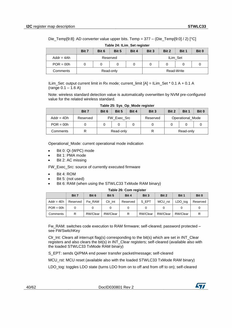
Die_Temp[9:8]: AD converter value upper bits. Temp = 377 – (Die_Temp[9:0] / 2) [°C]
Table 24: ILim_Set register
Bit 7 Bit 6 Bit 5 Bit 4 Bit 3 Bit 2 Bit 1 Bit 0
Addr = 4Ah Reserved ILim_Set
POR = 00h 0 0 0 0 0 0 0 0
Comments Read-only Read-Write
ILim_Set: output current limit in Rx mode; current_limit [A] = ILim_Set * 0.1 A + 0.1 A (range 0.1 – 1.6 A)
Note: wireless standard detection value is automatically overwritten by NVM pre-configured value for the related wireless standard.
Table 25: Sys_Op_Mode register
Bit 7 Bit 6 Bit 5 Bit 4 Bit 3 Bit 2 Bit 1 Bit 0
Addr = 4Dh Reserved FW_Exec_Src Reserved Operational_Mode
POR = 00h 0 0 0 0 0 0 0 0
Comments R Read-only R Read-only
Operational_Mode: current operational mode indication
Bit 0: Qi (WPC) mode
Bit 1: PMA mode
Bit 2: AC missing
FW_Exec_Src: source of currently executed firmware
Bit 4: ROM
Bit 5: (not used)
Bit 6: RAM (when using the STWLC33 TxMode RAM binary)
Table 26: Com register
Bit 7 Bit 6 Bit 5 Bit 4 Bit 3 Bit 2 Bit 1 Bit 0
Addr = 4Eh Reserved Fw_RAM Clr_Int Reserved S_EPT MCU_rst LDO_tog Reserved
POR = 00h 0 0 0 0 0 0 0 0
Comments R RW/Clear RW/Clear R RW/Clear RW/Clear RW/Clear R
Fw_RAM: switches code execution to RAM firmware; self-cleared; password protected – see FWSwitchKey
Clr_Int: Clears all interrupt flag(s) corresponding to the bit(s) which are set in INT_Clear registers and also clears the bit(s) in INT_Clear registers; self-cleared (available also with the loaded STWLC33 TxMode RAM binary)
S_EPT: sends Qi/PMA end power transfer packet/message; self-cleared
MCU_rst: MCU reset (available also with the loaded STWLC33 TxMode RAM binary)
LDO_tog: toggles LDO state (turns LDO from on to off and from off to on); self-cleared

STWLC33 I2C register map description
DocID030801 Rev 2 41/62
Table 27: FWSwitchKey register
Bit 7 Bit 6 Bit 5 Bit 4 Bit 3 Bit 2 Bit 1 Bit 0
Addr = 4Fh FWSwitchKey
POR = 00h 0 0 0 0 0 0 0 0
Comments Read-Write
FWSwitchKey: password protection; write value 5Ah before attempting to switch to RAM firmware execution (Com[6])
Table 28: Qi_Data_Send register
Bit 7 Bit 6 Bit 5 Bit 4 Bit 3 Bit 2 Bit 1 Bit 0
Addr = 50h Header
51h Data[0]
52h Data[1]
53h Data[2]
54h Data[3]
55h Data[4]
Comments Read-Write
The set of registers sends Qi packets (up to 5 byte long).
Header: Qi (WPC) packet header, see WPC specification [2] for valid headers. Packet length is derived from header value.
To send the packet, see Qi_Data_Send_Control register.
Table 29: RXID register
Bit 7 Bit 6 Bit 5 Bit 4 Bit 3 Bit 2 Bit 1 Bit 0
Addr = 5Ch RXID[0]
5Dh RXID[1]
5Eh RXID[2]
5Fh RXID[3]
60h RXID[4]
61h RXID[5]
Comments Read-only
RXID: based on operation mode – PMA or Qi (WPC) receiver ID (chip unique data stored in NVM). Data are valid after detecting the wireless standard.
Referring to Qi specification [2], to define the identification packet. RXID[0] corresponds to byte B3 and RXID[3] to B6. RXID[4] and [RXID5] have no meaning for Qi.
Referring to PMA specification [3], RXID[0] corresponds to MSByte and RXID[5] to LSByte.

I2C register map description STWLC33
42/62 DocID030801 Rev 2
Table 30: OVP_Set register
Bit 7 Bit 6 Bit 5 Bit 4 Bit 3 Bit 2 Bit 1 Bit 0
Addr = 62h Reserved Clamp_Voltage
POR = 00h 0 0 0 0 0 0 0 0
Comments Read-only Read-Write
Clamp_Voltage: clamping voltage setup (for OVP interrupt and for CL1/2 capacitive clamps)
000: 17 V
001: 20 V
010: 15 V
011: 13 V
100–111: 11 V
Note: wireless standard detection value is automatically overwritten by NVM pre-configured value for the related wireless standard.
Table 31: VRECT_L register
Bit 7 Bit 6 Bit 5 Bit 4 Bit 3 Bit 2 Bit 1 Bit 0
Addr = 64h VRECT[7:0]
POR = 00h 0 0 0 0 0 0 0 0
Comments Read-only
VRECT[7:0]: VRECT measured value lower bits
Table 32: VRECT_H register
Bit 7 Bit 6 Bit 5 Bit 4 Bit 3 Bit 2 Bit 1 Bit 0
Addr = 65h VRECT[15:8]
POR = 00h 0 0 0 0 0 0 0 0
Comments Read-only
VRECT[15:8]: VRECT measured value upper bits. Voltage = VRECT[15:0] * 1 mV
Table 33: VOUT_L register
Bit 7 Bit 6 Bit 5 Bit 4 Bit 3 Bit 2 Bit 1 Bit 0
Addr = 66h VOUT[7:0]
POR = 00h 0 0 0 0 0 0 0 0
Comments Read-only
VOUT[7:0]: VOUT measured value lower bits
Table 34: VOUT_H register
Bit 7 Bit 6 Bit 5 Bit 4 Bit 3 Bit 2 Bit 1 Bit 0
Addr = 67h ADC_VOUT[15:8]
POR = 00h 0 0 0 0 0 0 0 0
Comments Read-only

STWLC33 I2C register map description
DocID030801 Rev 2 43/62
VOUT[15:8]: VOUT measured value upper bits. Voltage = VOUT[15:0] * 1 mV
Table 35: PMA_ADV_L register
Bit 7 Bit 6 Bit 5 Bit 4 Bit 3 Bit 2 Bit 1 Bit 0
Addr = 78h PMA_ADV_MSG[3:0] PMA_ADV_CS
POR = 00h 0 0 0 0 0 0 0 0
Comments Read-only Read-only
PMA_ADV_CS: PMA advertisement Checksum
PMA_ADV_MSG[3:0]: PMA advertisement message, lower bits
Table 36: PMA_ADV_H register
Bit 7 Bit 6 Bit 5 Bit 4 Bit 3 Bit 2 Bit 1 Bit 0
Addr = 79h Reserved PMA_ADV_MSG[7:4]
POR = 00h 0 0 0 0 0 0 0 0
Comments Read-only Read-only
PMA_ADV_MSG[7:4]: PMA advertisement message, upper bits
Table 37: Op_Freq_L register
Bit 7 Bit 6 Bit 5 Bit 4 Bit 3 Bit 2 Bit 1 Bit 0
Addr = FAh Op_Freq[7:0]
POR = 00h 0 0 0 0 0 0 0 0
Comments Read-only
Op_Freq[7:0]: measured frequency, lower byte
Table 38: Op_Freq_H register
Bit 7 Bit 6 Bit 5 Bit 4 Bit 3 Bit 2 Bit 1 Bit 0
Addr = FBh Reserved Op_Freq[11:8]
POR = 00h 0 0 0 0 0 0 0 0
Comments Read-only Read-only
Op_Freq[11:8]: measured frequency, upper byte. Frequency = Op_Freq[11:0]*1 kHz
Table 39: Ping_Freq_L register
Bit 7 Bit 6 Bit 5 Bit 4 Bit 3 Bit 2 Bit 1 Bit 0
Addr = FCh Ping_Freq[7:0]
POR = 00h 0 0 0 0 0 0 0 0
Comments Read-only
Ping_Freq[7:0]: measured ping frequency, lower byte

I2C register map description STWLC33
44/62 DocID030801 Rev 2
Table 40: Ping_Freq_H register
Bit 7 Bit 6 Bit 5 Bit 4 Bit 3 Bit 2 Bit 1 Bit 0
Addr = FDh Reserved Ping_Freq[11:8]
POR = 00h 0 0 0 0 0 0 0 0
Comments Read-only Read-only
Ping_Freq[11:8]: measured ping frequency, upper byte. Frequency = Ping_Freq[11:0]*1 kHz
Table 41: PRMC_ID_L register
Bit 7 Bit 6 Bit 5 Bit 4 Bit 3 Bit 2 Bit 1 Bit 0
Addr = 80h PRMC_ID[7:0]
POR = 00h 0 0 0 0 0 0 0 0
Comments Read-only
PRMC_ID[7:0]: IC vendor Qi (WPC) PRMC ID for Rx mode, lower byte
Table 42: PRMC_ID_H register
Bit 7 Bit 6 Bit 5 Bit 4 Bit 3 Bit 2 Bit 1 Bit 0
Addr = 81h PRMC_ID[15:8]
POR = 00h 0 0 0 0 0 0 0 0
Comments Read-only
PRMC_ID[15:8]: IC vendor Qi (WPC) PRMC ID for Rx mode, upper byte
Referring to Qi specification [2], to define the identification packet. PRMC_ID_H refers to byte B1, PRMC_ID_L to B2.
Note: wireless standard detection value is automatically overwritten by NVM pre-configured value for the related wireless standard.
Table 43: Qi_Data_Send_Control register
Bit 7 Bit 6 Bit 5 Bit 4 Bit 3 Bit 2 Bit 1 Bit 0
Addr = 87h Priority Reserved Reserved Reserved Reserved Rcv_Dat Rcv_Pat Send
POR = 00h 0 0 0 0 0 0 0 0
Comments RW R R R R RW RW RW/Clear
Send: schedules sending the packet
Rcv_Pat: if set the STWLC33 enables FSK demodulator to receive pattern response from the transmitter after sending the packet
Rcv_Dat: if set the STWLC33 enables FSK demodulator to receive data response from the transmitter after sending the packet
Priority: if set the STWLC33 sends the packet immediately even if it causes violation of Qi timing specification for control error or received power packets. Use this feature carefully.
STWLC33 I2C register map description
DocID030801 Rev 2 45/62
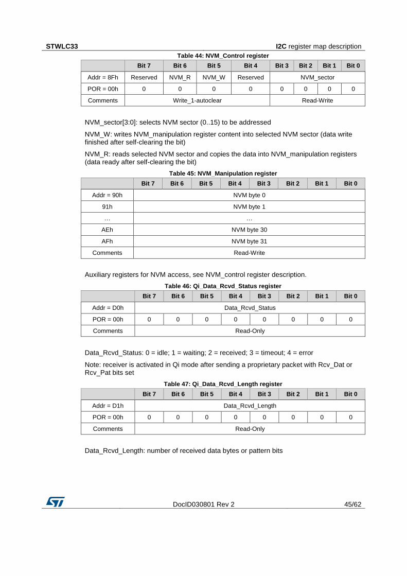
Table 44: NVM_Control register
Bit 7 Bit 6 Bit 5 Bit 4 Bit 3 Bit 2 Bit 1 Bit 0
Addr = 8Fh Reserved NVM_R NVM_W Reserved NVM_sector
POR = 00h 0 0 0 0 0 0 0 0
Comments Write_1-autoclear Read-Write
NVM_sector[3:0]: selects NVM sector (0..15) to be addressed
NVM_W: writes NVM_manipulation register content into selected NVM sector (data write finished after self-clearing the bit)
NVM_R: reads selected NVM sector and copies the data into NVM_manipulation registers (data ready after self-clearing the bit)
Table 45: NVM_Manipulation register
Bit 7 Bit 6 Bit 5 Bit 4 Bit 3 Bit 2 Bit 1 Bit 0
Addr = 90h NVM byte 0
91h NVM byte 1
… …
AEh NVM byte 30
AFh NVM byte 31
Comments Read-Write
Auxiliary registers for NVM access, see NVM_control register description.
Table 46: Qi_Data_Rcvd_Status register
Bit 7 Bit 6 Bit 5 Bit 4 Bit 3 Bit 2 Bit 1 Bit 0
Addr = D0h Data_Rcvd_Status
POR = 00h 0 0 0 0 0 0 0 0
Comments Read-Only
Data_Rcvd_Status: 0 = idle; 1 = waiting; 2 = received; 3 = timeout; 4 = error
Note: receiver is activated in Qi mode after sending a proprietary packet with Rcv_Dat or Rcv_Pat bits set
Table 47: Qi_Data_Rcvd_Length register
Bit 7 Bit 6 Bit 5 Bit 4 Bit 3 Bit 2 Bit 1 Bit 0
Addr = D1h Data_Rcvd_Length
POR = 00h 0 0 0 0 0 0 0 0
Comments Read-Only
Data_Rcvd_Length: number of received data bytes or pattern bits

I2C register map description STWLC33
46/62 DocID030801 Rev 2
Table 48: Qi_Data_Rcvd_Format register
Bit 7 Bit 6 Bit 5 Bit 4 Bit 3 Bit 2 Bit 1 Bit 0
Addr = D2h Data_Rcvd_Format
POR = 00h 0 0 0 0 0 0 0 0
Comments Read-only
Data_Rcvd_Format: 1 = pattern; 2 = data
Table 49: Qi_Data_Rcvd register
Bit 7 Bit 6 Bit 5 Bit 4 Bit 3 Bit 2 Bit 1 Bit 0
Addr = D3h Data[0] or pattern
D4h Data[1]
D5h Data[2]
D6h Data[3]
D7h Data[4]
Comments Read-only
Pattern: FFh for ACK, 00h for NAK and 55h for ND. Note that the response may not contain all bits, e.g. FEh or 7Fh should be also recognized as ACK
Data: all received data including checksum byte
Table 50: Qi_Power_Transfer_Contract register
Bit 7 Bit 6 Bit 5 Bit 4 Bit 3 Bit 2 Bit 1 Bit 0
Addr = F6h Guaranteed power
F7h Maximum power
F8h RxPwr format
F9h FSK configuration
Comments Read-only
These registers contain the values of valid power transfer contract. Registers are updated after successful (acknowledged) Qi negotiation phase.
Table 51: Max_Freq_Tx_L register
Bit 7 Bit 6 Bit 5 Bit 4 Bit 3 Bit 2 Bit 1 Bit 0
Addr = 10h Max_Freq_Tx[7:0]
POR = 9Ch 1 0 0 1 1 1 0 0
Comments Read-Write
Max_Freq_Tx[7:0]: maximal operation frequency in Tx mode, lower byte
Note: available with the loaded STWLC33 TxMode RAM binary only.

STWLC33 I2C register map description
DocID030801 Rev 2 47/62
Table 52: Max_Freq_Tx_H register
Bit 7 Bit 6 Bit 5 Bit 4 Bit 3 Bit 2 Bit 1 Bit 0
Addr = 11h Max_Freq_Tx[15:8]
POR = 00h 0 0 0 0 0 0 0 0
Comments Read-Write
Max_Freq_Tx[15:8]: maximal operation frequency in Tx mode, upper byte. Frequency f = 32 MHz / Max_Freq_Tx[15:0]. Default value 205 kHz
Note: available with the loaded STWLC33 TxMode RAM binary only.
Table 53: Min_Freq_Tx_L register
Bit 7 Bit 6 Bit 5 Bit 4 Bit 3 Bit 2 Bit 1 Bit 0
Addr = 12h Min_Freq_Tx[7:0]
POR = 22h 0 0 1 0 0 0 1 0
Comments Read-Write
Min_Freq_Tx[7:0]: minimal operation frequency in Tx mode, lower byte
Note: available with the loaded STWLC33 TxMode RAM binary only.
Table 54: Min_Freq_Tx_H register
Bit 7 Bit 6 Bit 5 Bit 4 Bit 3 Bit 2 Bit 1 Bit 0
Addr = 13h Min_Freq_Tx[15:8]
POR = 01h 0 0 0 0 0 0 0 1
Comments Read-Write
Min_Freq_Tx[15:8]: minimal operation frequency in Tx mode, upper byte. Frequency f = 32 MHz / Min_Freq_Tx[15:0]. Default value 110 kHz
Note: available with the loaded STWLC33 TxMode RAM binary only.
Table 55: Ping_Freq_Tx_L register
Bit 7 Bit 6 Bit 5 Bit 4 Bit 3 Bit 2 Bit 1 Bit 0
Addr = 14h Ping_Freq_Tx[7:0]
POR = C8h 1 1 0 0 1 0 0 0
Comments Read-Write
Ping_Freq_Tx[7:0]: Tx ping frequency, lower byte
Note: available with the loaded STWLC33 TxMode RAM binary only
Table 56: Ping_Freq_Tx_H register
Bit 7 Bit 6 Bit 5 Bit 4 Bit 3 Bit 2 Bit 1 Bit 0
Addr = 15h Ping_Freq_Tx[15:8]
POR = 00h 0 0 0 0 0 0 0 0
Comments Read-Write

I2C register map description STWLC33
48/62 DocID030801 Rev 2
Ping_Freq_Tx[15:8]: Tx ping frequency, upper byte. Frequency f = 32 MHz / Ping_Freq_Tx[15:0]. Default value 160 kHz
Note: available with the loaded STWLC33 TxMode RAM binary only.
Table 57: ASK_High_Thr_Tx register
Bit 7 Bit 6 Bit 5 Bit 4 Bit 3 Bit 2 Bit 1 Bit 0
Addr = 16h ASK_High_Thr_Tx[7:0]
POR = 28h 0 0 1 0 1 0 0 0
Comments Read-write
ASK_High_Thr_Tx[7:0]: ASK demodulator relative threshold – positive polarity
Note: available with the loaded STWLC33 TxMode RAM binary only.
Table 58: ASK_Low_Thr_Tx register
Bit 7 Bit 6 Bit 5 Bit 4 Bit 3 Bit 2 Bit 1 Bit 0
Addr = 17h ASK_Low_Thr_Tx[7:0]
POR = 28h 0 0 1 0 1 0 0 0
Comments Read-write
ASK_Low_Thr_Tx[7:0]: ASK demodulator relative threshold – negative polarity
Note: available with the loaded STWLC33 TxMode RAM binary only.
Table 59: RxPower_Rcvd_Value_Tx register
Bit 7 Bit 6 Bit 5 Bit 4 Bit 3 Bit 2 Bit 1 Bit 0
Addr = 1Ch RxPower_Rcvd_Value_Tx[7:0]
POR = 00h 0 0 0 0 0 0 0 0
Comments Read-only
RxPower_Rcvd_Value_Tx[7:0]: last value received in RxPower packet from the receiver
Note: available with the loaded STWLC33 TxMode RAM binary only
Table 60: EPT_Reason_Tx register
Bit 7 Bit 6 Bit 5 Bit 4 Bit 3 Bit 2 Bit 1 Bit 0
Addr = 1Dh EPT_Reason_Tx[7:0]
POR = 00h 0 0 0 0 0 0 0 0
Comments Read-only
EPT_Reason_Tx[7:0]: last reason of end power transfer:
00h: EPT not happened yet
01h: control error packet timeout (1800 ms)
02h: received power packet timeout (24000 ms)
03h: packet order not comply with Qi spec
04h: Tx overtemperature
05h: Tx overcurrent
06h: FOD error

STWLC33 I2C register map description
DocID030801 Rev 2 49/62
10h – 1Bh: received end power transfer packet with value 00h – 0Bh
1Ch: received end power transfer packet with invalid value
Note: available with the loaded STWLC33 TxMode RAM binary only, see Section 13: "Procedure to load executable binary".
Table 61: Status_Tx register
Bit 7 Bit 6 Bit 5 Bit 4 Bit 3 Bit 2 Bit 1 Bit 0
Addr = 35h Reserved TX_OCP TX_OTP Reserved TX_CON Reserved
POR = 00h 0 0 0 0 0 0 0 0
Comments R R R R R Read-only
TX_OCP: Tx mode overcurrent; 0 = normal condition; 1 = overcurrent (power transfer is automatically terminated)
TX_OTP: Tx mode temperature status; 0 = normal condition; 1 = overtemperature (power transfer is automatically terminated)
TX_CON: Tx mode power transfer status; 0 = not in power transfer; 1 = in power transfer
Note: available with the loaded STWLC33 TxMode RAM binary only
Table 62: INT_Tx register
Bit 7 Bit 6 Bit 5 Bit 4 Bit 3 Bit 2 Bit 1 Bit 0
Addr = 37h Reserved TX_OCP TX_OTP Reserved TX_CON Reserved
POR = 00h 0 0 0 0 0 0 0 0
Comments R R R R R Read-only
TX_OCP: 1 = indicates pending interrupt; (interrupt triggered on setting of TX_OCP bit in Status_Tx register)
TX_OTP: 1 = indicates pending interrupt; (interrupt triggered on setting of TX_OTP bit in Status_Tx register)
TX_CON: 1 = indicates pending interrupt; (interrupt triggered on any change of TX_CON bit in Status_Tx register)
Note: available with the loaded STWLC33 TxMode RAM binary only.
Table 63: INT_Enable_Tx register
Bit 7 Bit 6 Bit 5 Bit 4 Bit 3 Bit 2 Bit 1 Bit 0
Addr = 39h Reserved TX_OCP TX_OTP Reserved TX_CON Reserved
POR = 00h 0 0 0 0 0 0 0 0
Comments RW RW RW RW RW Read-Write
TX_OCP: 0 = INT pin output disabled; 1 = INT pin output enabled
TX_OTP: 0 = INT pin output disabled; 1 = INT pin output enabled
TX_CON: 0 = INT pin output disabled; 1 = INT pin output enabled
Note: available with the loaded STWLC33 TxMode RAM binary only.

I2C register map description STWLC33
50/62 DocID030801 Rev 2
Table 64: VRECT_Tx_L register
Bit 7 Bit 6 Bit 5 Bit 4 Bit 3 Bit 2 Bit 1 Bit 0
Addr = 40h VRECT_Tx[7:0]
POR = 00h 0 0 0 0 0 0 0 0
Comments Read-only
VRECT_Tx[7:0]: measured VRECT voltage lower bits
Note: available with the loaded STWLC33 TxMode RAM binary only.
Table 65: VRECT_Tx_H register
Bit 7 Bit 6 Bit 5 Bit 4 Bit 3 Bit 2 Bit 1 Bit 0
Addr = 41h VRECT_Tx[15:8]
POR = 00h 0 0 0 0 0 0 0 0
Comments Read-only
VRECT_Tx[15:8]: measured VRECT voltage upper bits, voltage = VRECT_Tx[15:0] * 1 mV
Note: available with the loaded STWLC33 TxMode RAM binary only.
Table 66: IIN_Tx_L register
Bit 7 Bit 6 Bit 5 Bit 4 Bit 3 Bit 2 Bit 1 Bit 0
Addr = 42h IIN_Tx[7:0]
POR = 00h 0 0 0 0 0 0 0 0
Comments Read-only
IIN_Tx[7:0]: measured IIN (OUT pin current) lower bits
Note: available with the loaded STWLC33 TxMode RAM binary only.
Table 67: IIN_Tx_H register
Bit 7 Bit 6 Bit 5 Bit 4 Bit 3 Bit 2 Bit 1 Bit 0
Addr = 43h IIN_Tx[15:8]
POR = 00h 0 0 0 0 0 0 0 0
Comments Read-only
IIN_Tx[15:8]: measured IIN (OUT pin current) upper bits, current = IIN_Tx[15:0] * 1 mA
Note: available with the loaded STWLC33 TxMode RAM binary only.
Table 68: INT_Clear_Tx register
Bit 7 Bit 6 Bit 5 Bit 4 Bit 3 Bit 2 Bit 1 Bit 0
Addr = 4Bh Reserved TX_OCP TX_OTP Reserved TX_CON Reserved
POR = 00h 0 0 0 0 0 0 0 0
Comments RW RW/Clear RW/Clear RW RW/Clear Read-Write

STWLC33 I2C register map description
DocID030801 Rev 2 51/62
TX_OCP: writes 1 to enable clearing of the corresponding bit in INT_Tx register; auto-cleared from Com registers, Clr_Int bit
TX_OTP: writes 1 to enable clearing of the corresponding bit in INT_Tx register; auto-cleared from Com registers, Clr_Int bit
TX_CON: writes 1 to enable clearing of the corresponding bit in INT_Tx register; auto-cleared from Com registers, Clr_Int bit
Note: available with the loaded STWLC33 TxMode RAM binary only, see Section 13: "Procedure to load executable binary".
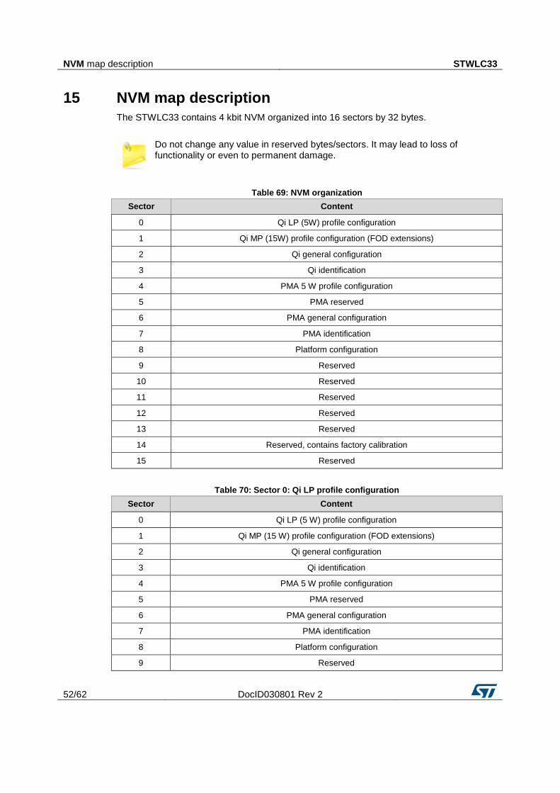
NVM map description STWLC33
52/62 DocID030801 Rev 2
15 NVM map description
The STWLC33 contains 4 kbit NVM organized into 16 sectors by 32 bytes.
Do not change any value in reserved bytes/sectors. It may lead to loss of functionality or even to permanent damage.
Table 69: NVM organization
Sector Content
0 Qi LP (5W) profile configuration
1 Qi MP (15W) profile configuration (FOD extensions)
2 Qi general configuration
3 Qi identification
4 PMA 5 W profile configuration
5 PMA reserved
6 PMA general configuration
7 PMA identification
8 Platform configuration
9 Reserved
10 Reserved
11 Reserved
12 Reserved
13 Reserved
14 Reserved, contains factory calibration
15 Reserved
Table 70: Sector 0: Qi LP profile configuration
Sector Content
0 Qi LP (5 W) profile configuration
1 Qi MP (15 W) profile configuration (FOD extensions)
2 Qi general configuration
3 Qi identification
4 PMA 5 W profile configuration
5 PMA reserved
6 PMA general configuration
7 PMA identification
8 Platform configuration
9 Reserved

STWLC33 NVM map description
DocID030801 Rev 2 53/62
Sector Content
10 Reserved
11 Reserved
12 Reserved
13 Reserved
14 Reserved, contains factory calibration
15 Reserved
This sector defines the power receiver variables in case Qi wireless standard is detected and Qi negotiation phase has not finished yet or new guaranteed power has not negotiated.
Table 71: Sector 1: Qi MP profile configuration
Bit 7 Bit 6 Bit 5 Bit 4 Bit 3 Bit 2 Bit 1 Bit 0 Default
Byte 0 Reserved 4B
Byte 1 Reserved 3D
Byte 2 Reserved 25
Byte 3 Reserved 66
Byte 4 Reserved 14
Byte 5 Reserved A2
Byte 6 Reserved 0F
Byte 7 Reserved Reserved 0D
Byte 8 VOUT voltage; VOUT = value * 0.1 V + 3.5 V 41
Byte 9
Reserved Input current limit; Ilim = value * 0.1 A + 0.1 A 2F
Byte 10 Reserved 89
Byte 11 Reserved Reserved 07
Byte 12
Reserved
Reserved 26
Byte 13 Reserved 00
Byte 14 Reserved 00
Byte 15 Reserved 3C
Byte 16 FOD_A correction LSB 72
Byte 17 FOD_A correction MSB 02
Byte 18 FOD_B correction;
RxPwr_corrected (16-bit value) = RxPwr * 128 / FOD_B + FOD_A 85
Byte 19 Reserved 02
Byte 20 Reserved 14
Byte 21 Reserved 00
Byte 22 External NTC threshold; threshold = value * 1.46 mV; 0 = disabled 00
Byte 23 Reserved 02
Byte 24 Reserved 04
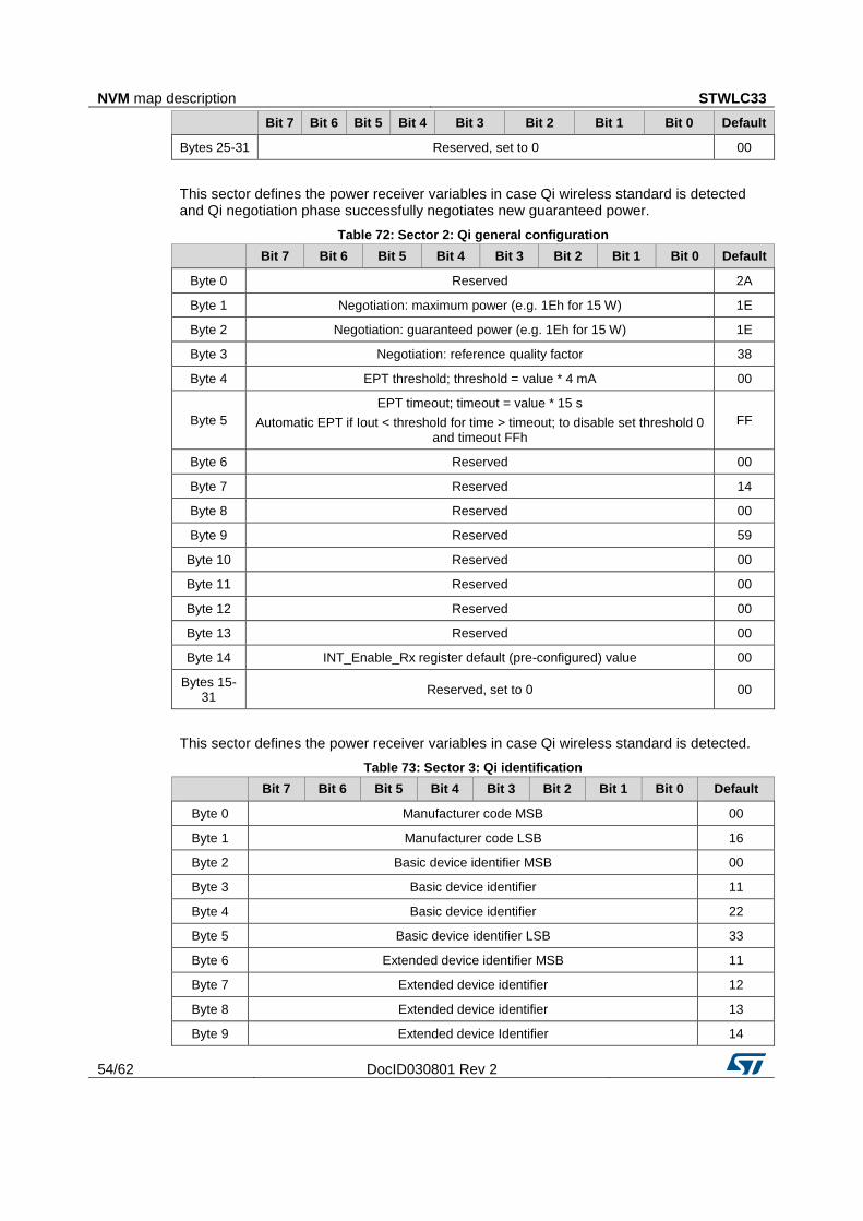
NVM map description STWLC33
54/62 DocID030801 Rev 2
Bit 7 Bit 6 Bit 5 Bit 4 Bit 3 Bit 2 Bit 1 Bit 0 Default
Bytes 25-31 Reserved, set to 0 00
This sector defines the power receiver variables in case Qi wireless standard is detected and Qi negotiation phase successfully negotiates new guaranteed power.
Table 72: Sector 2: Qi general configuration
Bit 7 Bit 6 Bit 5 Bit 4 Bit 3 Bit 2 Bit 1 Bit 0 Default
Byte 0 Reserved 2A
Byte 1 Negotiation: maximum power (e.g. 1Eh for 15 W) 1E
Byte 2 Negotiation: guaranteed power (e.g. 1Eh for 15 W) 1E
Byte 3 Negotiation: reference quality factor 38
Byte 4 EPT threshold; threshold = value * 4 mA 00
Byte 5
EPT timeout; timeout = value * 15 s
Automatic EPT if Iout < threshold for time > timeout; to disable set threshold 0 and timeout FFh
FF
Byte 6 Reserved 00
Byte 7 Reserved 14
Byte 8 Reserved 00
Byte 9 Reserved 59
Byte 10 Reserved 00
Byte 11 Reserved 00
Byte 12 Reserved 00
Byte 13 Reserved 00
Byte 14 INT_Enable_Rx register default (pre-configured) value 00
Bytes 15-31
Reserved, set to 0 00
This sector defines the power receiver variables in case Qi wireless standard is detected.
Table 73: Sector 3: Qi identification
Bit 7 Bit 6 Bit 5 Bit 4 Bit 3 Bit 2 Bit 1 Bit 0 Default
Byte 0 Manufacturer code MSB 00
Byte 1 Manufacturer code LSB 16
Byte 2 Basic device identifier MSB 00
Byte 3 Basic device identifier 11
Byte 4 Basic device identifier 22
Byte 5 Basic device identifier LSB 33
Byte 6 Extended device identifier MSB 11
Byte 7 Extended device identifier 12
Byte 8 Extended device identifier 13
Byte 9 Extended device Identifier 14
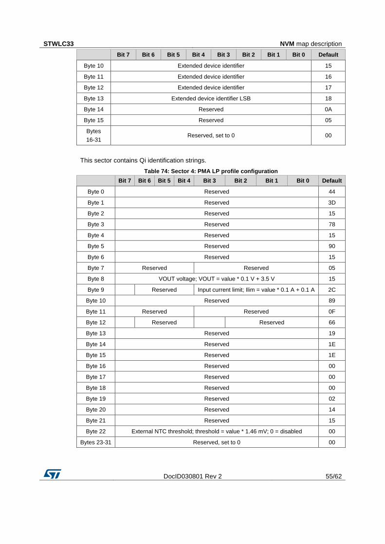
STWLC33 NVM map description
DocID030801 Rev 2 55/62
Bit 7 Bit 6 Bit 5 Bit 4 Bit 3 Bit 2 Bit 1 Bit 0 Default
Byte 10 Extended device identifier 15
Byte 11 Extended device identifier 16
Byte 12 Extended device identifier 17
Byte 13 Extended device identifier LSB 18
Byte 14 Reserved 0A
Byte 15 Reserved 05
Bytes
16-31 Reserved, set to 0 00
This sector contains Qi identification strings.
Table 74: Sector 4: PMA LP profile configuration
Bit 7 Bit 6 Bit 5 Bit 4 Bit 3 Bit 2 Bit 1 Bit 0 Default
Byte 0 Reserved 44
Byte 1 Reserved 3D
Byte 2 Reserved 15
Byte 3 Reserved 78
Byte 4 Reserved 15
Byte 5 Reserved 90
Byte 6 Reserved 15
Byte 7 Reserved Reserved 05
Byte 8 VOUT voltage; VOUT = value * 0.1 V + 3.5 V 15
Byte 9
Reserved Input current limit; Ilim = value * 0.1 A + 0.1 A 2C
Byte 10 Reserved 89
Byte 11 Reserved Reserved 0F
Byte 12
Reserved
Reserved 66
Byte 13 Reserved 19
Byte 14 Reserved 1E
Byte 15 Reserved 1E
Byte 16 Reserved 00
Byte 17 Reserved 00
Byte 18 Reserved 00
Byte 19 Reserved 02
Byte 20 Reserved 14
Byte 21 Reserved 15
Byte 22 External NTC threshold; threshold = value * 1.46 mV; 0 = disabled 00
Bytes 23-31 Reserved, set to 0 00

NVM map description STWLC33
56/62 DocID030801 Rev 2
This sector defines the power receiver variables if PMA wireless standard is detected.
Table 75: Sector 6: PMA general configuration
Bit 7 Bit 6 Bit 5 Bit 4 Bit 3 Bit 2 Bit 1 Bit 0 Default
Byte 0 Reserved Reserved 38
Byte 1 Reserved 03
Byte 2 Reserved 00
Byte 3 Reserved 00
Byte 4 Reserved 00
Byte 5 EOC threshold; threshold = value * 4 mA 25
Byte 6
EOC timeout; timeout = value * 15 s
Automatic EOC if Iout < threshold for time > timeout; to disable set threshold 0 and timeout FFh
8C
Byte 7 Reserved 07
Byte 8 Reserved 03
Byte 9 Reserved 56
Byte 10 Reserved 00
Byte 11 Reserved 00
Byte 12 Reserved 00
Byte 13 Reserved 00
Byte 14 INT_Enable_Rx register default (pre-configured) value 00
Byte 15 Reserved 00
Bytes 16-31
Reserved, set to 0 00
This sector defines the power receiver variables if PMA wireless standard is detected.
Table 76: Sector 7: PMA identification
Bit 7 Bit 6 Bit 5 Bit 4 Bit 3 Bit 2 Bit 1 Bit 0 Default
Byte 0 Preamble byte (00h) 00
Byte 1 Message ID (AAh) AA
Byte 2 Certification version 10
Byte 3 PMA ID LSB 00
Byte 4 PMA ID 00
Byte 5 PMA ID 00
Byte 6 PMA ID 25
Byte 7 PMA ID 50
Byte 8 PMA ID MSB 02
Byte 9 PMA ID CRC LSB 63
Byte 10 PMA ID CRC MSB 25

STWLC33 NVM map description
DocID030801 Rev 2 57/62
Bit 7 Bit 6 Bit 5 Bit 4 Bit 3 Bit 2 Bit 1 Bit 0 Default
Bytes
11-31 Reserved, set to 0 00
This sector contains PMA identification data.
Table 77: Sector 8: Platform configuration
Bit 7 Bit 6 Bit 5 Bit 4 Bit 3 Bit 2 Bit 1 Bit 0 Default
Byte 0 FOD_C (LSB) 9A
Byte 1 FOD_C (MSB) 01
Byte 2 GPIO2 function selection 01
Byte 3 GPIO1 function selection 00
Byte 4 GPIO0 function selection 03
Byte 5 GPIO3 function selection 00
Byte 6 GPIO4 function selection 00
Bytes
7-31 Reserved, set to 0 00
FOD_C: 16-bit value that represents a model value for RxCoil losses (“equivalent Rx coil resistance”). Value is in Ohms multiplied by 1024.
GPIO0 function selection: 0 = no function assigned, pin remains in HiZ state; 1 = power good push-pull output signal (H = in power transfer); 2 = power good push-pull output signal inverted (L=in power transfer); 3 = Qi medium power negotiated push-pull output (H = MP, L = LP); 4 = Qi medium power negotiated push-pull output inverted (H = LP, L = MP).
GPIO1 function selection: 0 = no function assigned, pin remains in HiZ state; 1 = power good open-drain output signal (L=in power transfer, open=not in power transfer); 2 = Qi medium power negotiated open-drain output signal (L=MP, open=LP).
GPIO2 function selection: 0 = no function assigned, pin remains in HiZ state; 1 = power good push-pull output signal (H=in power transfer); 2 = power good push-pull output signal inverted (L=in power transfer); 3 = Qi medium power negotiated push-pull output (H = MP, L = LP); 4 = Qi medium power negotiated push-pull output inverted (H = LP, L = MP).
GPIO3 function selection: 0 = no function assigned, pin remains in HiZ state with internal weak pull-up. (Do not tie low during the device startup).
GPIO4 function selection: 0 = no function assigned, pin remains in HiZ state; 1 = power good open-drain output signal (L = in power transfer, open = not in power transfer); 2 = Qi medium power negotiated open-drain output signal (L = MP, open = LP).

Package information STWLC33
58/62 DocID030801 Rev 2
16 Package information
In order to meet environmental requirements, ST offers these devices in different grades of ECOPACK® packages, depending on their level of environmental compliance. ECOPACK® specifications, grade definitions and product status are available at: www.st.com. ECOPACK® is an ST trademark.
16.1 Flip Chip 52 bumps (3.97x2.67 mm) package information
Figure 19: Flip Chip (3.97x2.67 mm) package outline

STWLC33 Package information
DocID030801 Rev 2 59/62
Table 78: Flip Chip (3.97x2.67 mm) package mechanical data
Dim. mm
Min. Typ. Max.
A 0.545 0.600 0.655
A1 0.170 0.200 0.230
A2 0.350 0.375 0.400
b 0.230 0.260 0.290
D 3.910 3.940 3.970
D1
3.20
E 2.610 2.640 2.670
E1
2.00
e
0.40
SE
0.20
fD
0.370
fE
0.320
$
0.025
ccc
0.060
The terminal A1 on the bump side is identified by a distinguishing feature (for instance by a circular "clear area", typically 0.1 mm diameter) and/or a missing bump. The terminal A1 on the backside of the product is identified by a distinguishing feature (for instance by a circular "clear area", typically between 0.1 and 0.5 mm diameter, depending on the die size).
Figure 20: Flip Chip (3.97x2.67 mm) recommended footprint

Reference STWLC33
60/62 DocID030801 Rev 2
17 Reference
1. I2C bus specification and user manual; rev. 6 2. Qi wireless power transfer system; power class 0 specification; version 1.2.2 3. PMA inductive wireless power transfer receiver specification - system release 1
STWLC33 Revision history
DocID030801 Rev 2 61/62
18 Revision history Table 79: Document revision history
Date Revision Changes
25-Sep-2017 1 Initial release
13-Nov-2017 2 Updated features in cover page and Section 16.1: "Flip Chip 52 bumps (3.97x2.67 mm) package information".

STWLC33
62/62 DocID030801 Rev 2
IMPORTANT NOTICE – PLEASE READ CAREFULLY
STMicroelectronics NV and its subsidiaries (“ST”) reserve the right to make changes, corrections, enhancements, modifications , and improvements to ST products and/or to this document at any time without notice. Purchasers should obtain the latest relevant information on ST products before placing orders. ST products are sold pursuant to ST’s terms and conditions of sale in place at the time of order acknowledgement.
Purchasers are solely responsible for the choice, selection, and use of ST products and ST assumes no liability for application assistance or the design of Purchasers’ products.
No license, express or implied, to any intellectual property right is granted by ST herein.
Resale of ST products with provisions different from the information set forth herein shall void any warranty granted by ST for such product.
ST and the ST logo are trademarks of ST. All other product or service names are the property of their respective owners.
Information in this document supersedes and replaces information previously supplied in any prior versions of this document.
© 2017 STMicroelectronics – All rights reserved


![Investigation of living cells using JPK’s QI™ mode · tems QI™ mode is fully ... investigation of living cells with complementary tech-niques. ... [14]; here we used the contact](https://static.fdocuments.net/doc/165x107/5b76ffe57f8b9a4c438c2d20/investigation-of-living-cells-using-jpks-qi-mode-tems-qi-mode-is-fully.jpg)