Multi-level Signaling in High- density, High-speed ... · Multi-level Signaling in High-density,...
21
DesignCon 2008 Multi-level Signaling in High- density, High-speed Electrical Links Dong G. Kam, IBM T. J. Watson Research Center [email protected] Troy J. Beukema, IBM T. J. Watson Research Center Young H. Kwark, IBM T. J. Watson Research Center Lei Shan, IBM T. J. Watson Research Center Xiaoxiong Gu, IBM T. J. Watson Research Center Petar K. Pepeljugoski, IBM T. J. Watson Research Center Mark B. Ritter, IBM T. J. Watson Research Center
Transcript of Multi-level Signaling in High- density, High-speed ... · Multi-level Signaling in High-density,...

DesignCon 2008
Multi-level Signaling in High-density, High-speed Electrical Links Dong G. Kam, IBM T. J. Watson Research Center [email protected] Troy J. Beukema, IBM T. J. Watson Research Center Young H. Kwark, IBM T. J. Watson Research Center Lei Shan, IBM T. J. Watson Research Center Xiaoxiong Gu, IBM T. J. Watson Research Center Petar K. Pepeljugoski, IBM T. J. Watson Research Center Mark B. Ritter, IBM T. J. Watson Research Center
Abstract We present an analysis comparing multi-level signaling to standard NRZ signaling for module-to-module on-board electrical interconnects. To study on-board electrical performance, duobinary and PAM4 I/O models were created and compared to NRZ signaling in behavioral link-level simulations. A great variety of high-density, high-speed on-board module-to-module electrical links were analyzed, and specific interconnect channels were validated experimentally with programmable equalization transceiver chips communicating through a set of fabricated test structures. Link performance was measured with on-chip eye monitoring circuits and an oscilloscope. Simulation results show that NRZ signaling with FFE and DFE equalization offers the best electrical performance. Author(s) Biography Dong G. Kam received the B.S. degree in physics, the M.S. and Ph.D. degrees in electrical engineering from Korea Advanced Institute of Science and Technology, Daejeon, Korea, in 2000, 2002 and 2006, respectively. In 2007, he joined IBM T. J. Watson Research Center, Yorktown Heights, NY, where he works on high-speed I/O subsystem design, and electromagnetic modeling and characterization of high-speed interconnects and microelectronic packages. Troy J. Beukema received the B.S.E.E. and M.S.E.E. degrees from Michigan Technological University in 1984 and 1988, respectively. In 1996, he joined IBM T. J. Watson Research Center, where he is presently a Research Staff Member concentrating in the areas of radio architecture and modulation for 60 GHz wireless systems, and system designs for adaptive equalization of 6-12 Gb/s wireline serial I/O links. Young H. Kwark received his BSEE from the Massachusetts Institute of Technology and his MSEE/PhD from Stanford University. His work experience as a Research Staff Member at the IBM T. J. Watson Research Center includes circuit design for optical links and wireless applications. He is currently involved in package characterization for high performance computing platforms. Dr. Kwark received DesignCon Paper Awards in 2005 and 2006. Lei Shan received his B.S. in mechanical engineering from Zhejiang University in 1986 and the M.S. degree in electrical engineering and Ph.D. degree in mechanical engineering from Georgia Institute of Technology in 2000. In 2001, he joined IBM T.J. Watson Research Center as a Research Staff Member, where he works on high speed electronics/optoelectronics packaging designs.

Xiaoxiong Gu received the B.S. degree from Tsinghua University, Beijing, China, in 2000, the M.S. degree from the University of Missouri, Rolla, in 2002, and the Ph.D. degree from the University of Washington, Seattle, in 2006, all in electrical engineering. He is currently a Research Staff Member with the IBM T. J. Watson Research Center. His research interests include characterization of high-speed interconnect and microelectronic packaging, signal integrity and computational electromagnetics. Petar K. Pepeljugoski joined IBM Research as a Research Staff Member in 1994 after receiving his Ph.D. from U.C. Berkeley. His research work included design, modeling, prototyping, and characterization of MMF LAN links and parallel interconnects. He was involved in the development of several Ethernet (IEEE 802.3z, IEEE 802.3ae, IEEE 802.3aq) standards, as well as the development of the specification of the OM3 fiber, and subsequently recognized for his contributions. Dr. Pepeljugoski is an author or coauthor of more than 50 journal or conference articles and is a Senior Member of IEEE. Mark B. Ritter received a B.S. degree in physics from Montana State University in 1981 and M.S., M.Phil. and Ph.D. degrees in applied physics from Yale University in 1987. His work at IBM has focused on high-speed I/O circuit and package design, with work including Fibre Channel, 10 Gb/s Ethernet, and 40 Gb/s analog front end circuits as well as interconnect structures for high-speed data transmission. Dr. Ritter presently manages a group focusing on high-speed I/O subsystems, including electromagnetic characterization, link modeling, and subsystem analysis with an eye to optimizing I/O link performance metrics, whether electrical or optical. Dr. Ritter was the recipient of the 1982 American Physical Society Apker Award.
1. Introduction
Off-chip bandwidth requirements continue to grow to meet the needs of multi-core processor architectures. Electrical I/O research has focused on improving transceiver circuits to sustain the growth of data rates overcoming the limitations of the given integrated circuit technology. Although this approach has worked well in the past, the nature of link design is changing. Deep sub-micron CMOS I/O circuits can function at higher speeds than the channel bandwidth will support [1]. Passive performance improvement has been achieved through package advances incorporating the use of low-loss materials, innovative via-hole techniques, and new connector technologies. Active solutions strive to increase the link throughput by using signal processing. Pre-emphasis can be used to flatten the steep roll-off of channel’s insertion loss, and adaptive equalization seeks to remove inter-symbol interference (ISI). Alternative multi-level signaling schemes have also received much attention of late because they reduce channel bandwidth requirements at the cost of signal-to-noise ratio (SNR). Historically, they were widely used for communication over bandwidth limited channels. For example, Gigabit Ethernet uses pulse-amplitude modulation with five signal levels (PAM5) for communication over copper twisted pairs in a local area network (LAN). Recently, high-speed link designs have considered using a variety of multi-level signaling schemes [2, 3]. For instance, in the development of specifications such as the Optical Internetworking Forum (OIF)’s Common Electrical Interface at 25 Gb/s (CEI-25), duobinary and PAM4 have been discussed as alternatives to non-return-to-zero (NRZ) modulation [4]. The authors have been investigating the limits of electrical interconnect performance of future advanced packaging technologies. Although high-speed electrical links have been demonstrated previously [5, 6], our aim is to investigate very high-density, high-speed electrical buses utilizing a dense signal pitch which maximizes escape bandwidth with adequate signal integrity. A number of high-performance links have been analyzed from a holistic standpoint, considering I/O circuits and equalization, and including all levels of electrical packaging for module-to-module on-board applications. In this context, we wish to choose the modulation scheme which will optimize bus bandwidth. In this paper, we present simulations with a proprietary link modeling tool that allowed us to explore the effect of equalization and modulation formats at different data rates on link bit-error ratio (BER) and eye opening. Our link models have been validated with active, high-speed differential bus measurements utilizing a 16-channel link chip with programmable equalization and a per-channel data rate of up to 11 Gb/s. This chip is a product-level version of the prototype described in [7]. Using these models verified at 11 Gb/s, we extrapolate signaling performance to 25 Gb/s in order to explore the best signaling scheme to maximize data rates.
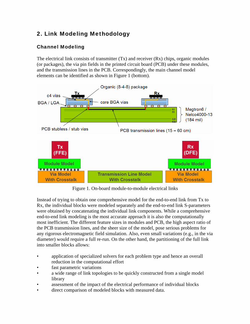
2. Link Modeling Methodology
Channel Modeling The electrical link consists of transmitter (Tx) and receiver (Rx) chips, organic modules (or packages), the via pin fields in the printed circuit board (PCB) under these modules, and the transmission lines in the PCB. Correspondingly, the main channel model elements can be identified as shown in Figure 1 (bottom).
Figure 1. On-board module-to-module electrical links
Instead of trying to obtain one comprehensive model for the end-to-end link from Tx to Rx, the individual blocks were modeled separately and the end-to-end link S-parameters were obtained by concatenating the individual link components. While a comprehensive end-to-end link modeling is the most accurate approach it is also the computationally most inefficient. The different feature sizes in modules and PCB, the high aspect ratio of the PCB transmission lines, and the sheer size of the model, pose serious problems for any rigorous electromagnetic field simulation. Also, even small variations (e.g., in the via diameter) would require a full re-run. On the other hand, the partitioning of the full link into smaller blocks allows: • application of specialized solvers for each problem type and hence an overall
reduction in the computational effort • fast parametric variations • a wide range of link topologies to be quickly constructed from a single model
library • assessment of the impact of the electrical performance of individual blocks • direct comparison of modeled blocks with measured data.

Full-wave simulations of the package elements including near and far-end crosstalk were concatenated to create 32-port S-parameter models of the entire signal path. Recessed-probe launch [8] measurements of the frequency-dependent dielectric loss of transmission line test coupons were used to refine transmission line models. Passive channel measurements to 50 GHz were taken with a 4-port vector network analyzer (VNA) to verify the S-parameter models. Unpopulated ball grid array (BGA) soldered modules allowed end-to-end passive channel measurements including all link elements except the chip wiring and controlled collapse chip connection (C4) balls on the transceiver chip (Figure 2).
Figure 2. End-to-end passive link measurement

These measurements agreed with corresponding channel models within ±1.5 dB at frequencies up to 10 GHz, and within ±2 dB up to 20 GHz as shown in the graph below. Much of the residual discrepancy was due to coupling to adjacent transmission lines which could not be terminated in the measurement as they were too numerous.
0.5
1.0
1.5
2.0
2.5
3.0
3.5
4.0
4.5
5.0
5.5
6.0
6.5
7.0
7.5
8.0
8.5
9.0
9.5
0.0
10
.0
-18
-16
-14
-12
-10
-8
-6
-4
-2
-20
0
freq, GHz
dB(M
egtr
on6_
4to1
_lon
g_S
9_B
B4P
_2..S
(1,2
))dB
(Meg
tron
6_4t
o1_l
ong_
S9_
BB
4P_2
..S(3
,4))
dB(S
(11,
27))
dB(S
(12,
28))
Figure 3. Single-ended insertion loss of differential wire pair on Hitachi Megtron6 low-
loss, half-stub cards: simulation (blue/red) vs. measurement (magenta/cyan) Full Link (including Tx and Rx) Modeling The models for link components such as transmission lines, vias, and modules, were collected to form a link component library (Figure 4) from which representative channels could be constructed. A representative next generation system architecture was used to estimate connectivity requirements for net lengths, number and length of through vias, and other interconnect electrical parameters. End-to-end S-parameter models of various interconnect channels were then formed through concatenation of relevant models from the component library. The performance of each channel was analyzed in the time domain through an internal IBM behavioral level link simulation tool. This tool models channel through and crosstalk response as well as random and deterministic jitter added by user-specified driver and receiver equalization architectures, and provides an estimate of BER given the data rate. The behavioral simulation is based on a linear time-invariant channel assumption, enabling fast convolution algorithms to be employed which result in simulation speed on the order of 1 Mb/minute. Traditional SPICE-based transient

simulation methods are orders of magnitude slower than this and cannot accurately capture low probability events and CDR dynamics without prohibitively long simulation times. Our behavioral link tool also provides eye diagrams and bathtub curves for link quality analysis. A scripting interface allows parameter studies and the exploration/classification of different link scenarios.
Figure 4. End-to-end link modeling methodology
For signaling comparison analysis, duobinary and PAM4 I/O models were created and included in behavioral link-level simulations. Duobinary takes advantage of the inherent roll-off of the backplane channel to help shape the data waveform. Duobinary data can be generated by sending NRZ data through a delay and sum filter, which has a Z-transform of 1+z-1. A low-pass filter is a reasonable approximation of this response. Since the typical response of a channel also resembles a low-pass filter, if we provide some additional filtering we can generate the required response from the cascade of the filter and the channel [2]. In our link modeling, the additional filtering was provided by a Tx feed-forward equalizer (FFE). The required response was generated from the cascade of the 4-tap FFE and the channel as shown in Figure 5-(a). Optimal tap coefficients were determined by minimum mean square error (MMSE) optimization routine, carried out in the time domain. The minimization constraints were error at the edge crossing and error at the data sample point. A frequency domain approach to optimization is also possible [9]. For duobinary signaling, it is necessary to reconvert the data stream to a binary sequence before a valid BER analysis can be done. A duobinary decoder was implemented by an Rx decision-feedback equalizer (DFE) which compensates for the partial response. Since the time dispersion added by FFE and channel continues for a long time, a DFE with more than three taps is generally required for optimal decoding (e.g. 5-tap DFE in Figure 5-(b)). PAM4 and NRZ I/O models were also created as shown in Figure 5-(c) and Figure 5-(d), respectively.

(a) Duobinary (b) Duobinary-to-binary data conversion
(c) PAM4 (d) NRZ
Figure 5. Eye diagrams of multi-level signaling based on generated I/O models
Full Link Model Validation End-to-end active link measurements with a 90-nm CMOS programmable 3-tap FFE, 5-tap DFE link chip with up to 16 full duplex channels operating up to 11 Gb/s were used to validate our link modeling. The link chips were mounted on organic modules which were in turn mounted on PCB test vehicles with soldered BGA or land grid array (LGA) connections, as shown in Figure 6. A wide variety of module-to-module link topologies and lengths were included in these test vehicles, which themselves were fabricated with a selection of advanced PCB fabrication materials and technologies. A digital interface to the link chips allowed automated control of link FFE equalization. The DFE tap coefficients were continuously updated by on-chip adaptation logic. Software control allowed exploration of different equalization and modulation approaches including no equalization, FFE or DFE only, FFE and DFE, and with proper programming even duobinary signaling. Link performance was measured with on-chip eye monitoring circuits. These measurements, which could also introduce controlled amounts of crosstalk, compared favorably with link simulations at 11 Gb/s for different channels and

equalization schemes (Figure 7). The eye opening was measured approximately at the confidence level of 10-3, and it was compared with eye simulation at the same BER.
Figure 6. Active link measurement with two LGA socketed modules
0
10
20
30
40
50
60
70
80
90
100
A0
A1
A2
A3
B0
B2
B3
A0
A1
A2
A3
B0
B2
B3
A0
A1
A2
A3
B0
B2
B3
A0
A1
A2
A3
B0
B2
B3
A0
A1
A2
A3
B0
B2
B3
A0
A1
A2
A3
B0
B2
B3
A0
A1
A2
A3
B0
B2
B3
A0
A1
A2
A3
B0
B2
B3
no EQ FFE only DFE only FFE+DFE no EQ FFE only DFE only FFE+DFE
45 cm 60 cm
Nor
mal
ized
Ver
tical
Eye
Ope
ning
[%]
Active measurementLink-level simulation
Figure 7. Active link model-hardware correlation

In order to see if we can match the appearance of the eye diagrams generated using our link models, the S-parameters of a link connecting the output of the Tx to a digital sampling oscilloscope (DSO) used on a different card for module screening were measured with the setup shown in Figure 8. This link consists of several segments: organic chip substrate, high speed pogo pin test socket, PCB (via array, transmission line, SMP launch), SMP to SMA adapter jumper, and SMA cable to the input of the DSO. Using the BGA clamp and after machining [8] an SMA to microwave probe adapter, the entire link was reconstructed using the actual SMP jumper and SMA cables as were used for the eye diagram measurements.
Figure 8. Reconstructed link used in the eye diagram measurements (upper left);
milling SMA to Probe Adapter (upper right); BGA Clamp over a dummy module with probe (lower left);
closeup of probe on C4 array (lower center); closeup of probe on SMA adapter (lower right)
An eye diagram was generated using these measured S-parameters and our link models including core parameters and FFE tap coefficients used for the duobinary measurements. Although this comparison is incomplete in that the impulse response of the DSO sampler should be considered as well, the two eye diagrams in Figure 9 show satisfactory correlation.
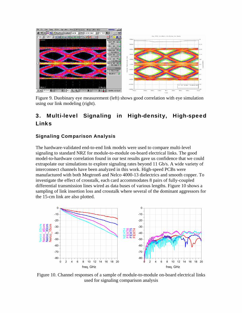
Figure 9. Duobinary eye measurement (left) shows good correlation with eye simulation using our link modeling (right). 3. Multi-level Signaling in High-density, High-speed Links
Signaling Comparison Analysis The hardware-validated end-to-end link models were used to compare multi-level signaling to standard NRZ for module-to-module on-board electrical links. The good model-to-hardware correlation found in our test results gave us confidence that we could extrapolate our simulations to explore signaling rates beyond 11 Gb/s. A wide variety of interconnect channels have been analyzed in this work. High-speed PCBs were manufactured with both Megtron6 and Nelco 4000-13 dielectrics and smooth copper. To investigate the effect of crosstalk, each card accommodates 8 pairs of fully-coupled differential transmission lines wired as data buses of various lengths. Figure 10 shows a sampling of link insertion loss and crosstalk where several of the dominant aggressors for the 15-cm link are also plotted.
2 4 6 8 10 12 14 16 180 20
-70
-60
-50
-40
-30
-20
-10
-80
0
freq, GHz
Ne
lco
_1
5cm
Ne
lco
_3
0cm
Ne
lco
_4
5cm
Ne
lco
_6
0cm
2 4 6 8 10 12 14 16 180 20
-70
-60
-50
-40
-30
-20
-10
-80
0
freq, GHz
FE
XT
4F
EX
T5
FE
XT
6N
EX
T4
Figure 10. Channel responses of a sample of module-to-module on-board electrical links
used for signaling comparison analysis

0
20
40
60
80
100
120
140
160
180
200
15G 20G 25G 15G 20G 25G 15G 20G 25G 15G 20G 25G 15G 20G 25G 15G 20G 25G 15G 20G 25G 15G 20G 25G
15cm 30cm 45cm 60cm 15cm 30cm 45cm 60cm
5-tap DFE 10-tap DFE
4-tap FFE
Vert
ical
Eye
Ope
ning
[mV]
NRZDUOPAM4
0
5
10
15
20
25
30
35
40
45
50
15G 20G 25G 15G 20G 25G 15G 20G 25G 15G 20G 25G 15G 20G 25G 15G 20G 25G 15G 20G 25G 15G 20G 25G
15cm 30cm 45cm 60cm 15cm 30cm 45cm 60cm
5-tap DFE 10-tap DFE
4-tap FFE
Hor
izon
tal E
ye O
peni
ng [p
s]
NRZDUOPAM4
Figure 11. Link performance comparison among signaling schemes
for module-to-module on-board electrical links

These channel models were analyzed with the link simulation tool. The I/O core models were scaled to 2x frequency to estimate performance at higher data rate than the core was designed to operate at. Duobinary and PAM4 were compared with NRZ for different DFE settings and data rate (Figure 11). A 4-tap symbol-spaced FFE with 1 pre-cursor and 2 post-cursors was assumed for all three signaling options, the launch was 800-mVpp differential, and the bit stream consisted of a 215-1 pseudo random bit sequence (PRBS). Both vertical eye opening and horizontal eye opening at the BER of 10-15 were used as a figure of merit. Overall, NRZ signaling with FFE and DFE equalization gives link performance superior to duobinary or PAM4 signaling. Representative eye diagrams and bathtub curves of each signaling method are shown in Figure 12.
Figure 12. Representative simulated eye diagrams and bathtub curves of signaling comparison analysis
NRZ
15-cm link w/ 5-tap DFE @ 25 Gb/s 45-cm link w/ 5-tap DFE @ 25 Gb/s
Duobinary
PAM4

Signaling Analysis on CEI-25 Standards The CEI standards group for 100 Gb/s Ethernet transceivers is focusing on physical layer (signaling) formats suitable for four-wide, 25 Gb/s electrical connections from switches to 100 Gb/s Ethernet optical transceivers. In this venue there were claims that duobinary and PAM4 signaling, respectively, provide better signal integrity than NRZ signaling. In this work, we employ our hardware-validated link modeling approach to study the achievable performance of duobinary, PAM4, and NRZ using a common FFE/DFE equalization system architecture. Although the data presented here does not necessarily represent the optimum achievable system performance for each signaling method, we believe the results present a fair relative performance assessment of each line signaling approach within a consistent equalization/modeling framework. The resulting data is useful to determine if one signaling format has a clear advantage over the others for application in a range of proposed 25 Gb/s test channels. Our modeling methodology was used to estimate the performance of various modulation formats over the reference channels [10, 11] provided by CEI-25 working group. In Figure 13, insertion loss and crosstalk responses are displayed. The parameters utilized in the simulations are listed below, which were assigned per the motions of the working group: • 215-1 PRBS data pattern • BER = 10-15 • Launch amplitude (victim/aggressor) = 800 mVpp • Tx DCD (duty-cycle distortion) = 0.035 UIpp (unit interval) • Rx reference frequency offset = 200 ppm • Random noise = 1.46 mVrms • Tx RJ (random jitter) = 0.15 UIpp @ 10-12 BER • Rx RJ = 0.15 UIpp @ 10-12 BER
2 4 6 8 10 12 14 16 180 20
-70
-60
-50
-40
-30
-20
-10
-80
0
freq, GHz
AL
U1
AL
U2
AL
U3
Mo
lex1
Mo
lex2
Mo
lex3
2 4 6 8 10 12 14 16 180 20
-70
-60
-50
-40
-30
-20
-10
-80
0
freq, GHz
ALU
_xta
lkM
olex
_xta
lk
Figure 13. Insertion loss and crosstalk responses of several reference channels for CEI-25

0
10
20
30
40
50
60
70
80
90
100
15G 20G 25G 15G 20G 25G 15G 20G 25G 15G 20G 25G 15G 20G 25G 15G 20G 25G
ALU1 ALU2 ALU3 ALU1 ALU2 ALU3
5-tap DFE 10-tap DFE
4-tap T-spaced FFE
Vert
ical
Eye
Ope
ning
[mV]
NRZDuobinaryPAM4
0
5
10
15
20
25
30
35
40
15G 20G 25G 15G 20G 25G 15G 20G 25G 15G 20G 25G 15G 20G 25G 15G 20G 25G
ALU1 ALU2 ALU3 ALU1 ALU2 ALU3
5-tap DFE 10-tap DFE
4-tap T-spaced FFE
Hor
izon
tal E
ye O
peni
ng [p
s]
NRZDuobinaryPAM4
Figure 14. Link performance comparison among signaling schemes for CEI-25 links [10]

0
10
20
30
40
50
15G 20G 25G 15G 20G 25G 15G 20G 25G 15G 20G 25G 15G 20G 25G 15G 20G 25G
Molex1 Molex2 Molex3 Molex1 Molex2 Molex3
5-tap DFE 10-tap DFE
4-tap T-spaced FFE
Vert
ical
Eye
Ope
ning
[mV]
NRZDuobinaryPAM4
0
5
10
15
20
25
15G 20G 25G 15G 20G 25G 15G 20G 25G 15G 20G 25G 15G 20G 25G 15G 20G 25G
Molex1 Molex2 Molex3 Molex1 Molex2 Molex3
5-tap DFE 10-tap DFE
4-tap T-spaced FFE
Hor
izon
tal E
ye O
peni
ng [p
s]
NRZDuobinaryPAM4
Figure 15. Link performance comparison among signaling schemes for CEI-25 links [11]

Although RJ was optimistically reduced for PAM4 by a factor of 2 (assuming the phase noise could drop at half the baud rate), PAM4 did not perform as well as NRZ. Duobinary signaling did not have any inherent advantage over NRZ either, as shown in Figure 14 and Figure 15. The data also shows a severe drop in performance for all signaling formats as the data-rate increases to the range of 20 to 25 Gb/s, indicating that the channels must be improved and/or the I/O equalization system design enhanced beyond the base-line FFE/DFE to achieve reliable operation in the range of 20 to 25 Gb/s. Conventional Wisdom of Multi-level Signaling Revisited A PAM4 transceiver divides a signal into four levels, which can be seen as three stacked eye patterns for every cycle. These are encoded as 00, 01, 10 and 11, allowing two bits to be encoded for every symbol time. As a result, the symbol rate with PAM4 is half that of NRZ, so the signal suffers less attenuation. The multi-level nature of PAM4 reduces the level spacing by a factor of 3 (9.5 dB). The common rationale is that if the slope of channel loss versus frequency is steep enough, the improvement in SNR due to baud rate reduction may be greater than 9.5 dB, justifying use of PAM4 [12]. For the channels studied, our simulations show that the lower channel bandwidth requirement does not result in a better SNR. For the 60-cm link in Figure 9, insertion loss at 12.5 GHz Nyquist frequency for NRZ is 12.4 dB higher than at 6.25 GHz Nyquist frequency for PAM4. Furthermore, the insertion loss difference at 12.5 GHz and 6.25 GHz is much bigger than 9.5 dB in every CEI-25 link (Figure 13). Yet, we could find no case where PAM4 showed an advantage over NRZ. This does not correlate with the conventional wisdom! In [7, 13], Bulzacchelli et al. explained this dilemma by focusing on the effect of DFE on insertion loss. DFE feedback is used to cancel ISI due to post-cursors in channel impulse response. To observe effect of DFE, they compared discrete Fourier transforms of the sampled channel response before and after eliminating post cursors. They found that elimination of these post-cursors flattens the frequency response; therefore, the conventional argument for using PAM4 in high-loss channels breaks down when DFE is applied to channel equalization. The 9.5 dB SNR penalty is actually just a rule of thumb. Four-level signaling is 3 times more sensitive to un-compensated ISI and crosstalk than NRZ since the peak signal to error threshold ratio is 3 times higher in PAM4 than NRZ. PAM4 systems therefore can require significantly more complicated DFE and/or crosstalk cancellation to be viable in challenging channels. Further, since the error threshold is 3 times smaller in PAM4 for a given transmit launch level, higher transmit launch level may be necessary to compensate for loss in receiver sensitivity, which is disadvantageous in low-voltage deep sub-micron CMOS technology. In [14], Liu and Caroselli indicated that crosstalk cancellation was necessary to achieve the necessary performance under the channel model and crosstalk assumptions made in the paper. However, crosstalk cancellation will be very difficult to realize in practical systems. The architecture of crosstalk cancellation is similar to that of DFE: noise at the sampling point is correlated against the aggressor’s source stream and

subtracted off in a linear summer at the sampling point. Many practical problems arise though, including causality/delay issues with FEXT channels and inter-core routing of high-speed lines in order to be able to design canceling receivers. The issue is made even worse for complex channels, typical in high-end computers, which often experience crosstalk from a number of sources, not necessarily near-neighbor I/O or even from the same bus! From our measurements and simulations we conclude that duobinary and PAM4 signaling do not perform as well as NRZ with FFE and DFE equalization for channels representative of those we anticipate in various high-speed, high-density computer and switch boards and backplanes. The tested links have significant loss and enough crosstalk that duobinary or PAM4 signaling produces closed eyes in many cases where NRZ was still able to provide some operating margin. Although it may be possible to improve performance of each line signaling approach by employing highly complex equalization system designs, practical considerations in the design of the I/O including power, area, and voltage limitations favor the relatively simple NRZ based system architecture in absence of a clear performance advantage of alternate signaling approaches. 4. Conclusions
In this paper, we introduced a link modeling methodology and hardware-validated end-to-end link models. Based on this, we presented a comprehensive analysis comparing multi-level signaling to standard NRZ signaling for a variety of high-density, high-speed electrical links. Simulation results show that NRZ signaling with FFE and DFE equalization offers the best link performance.

Acknowledgment
The authors would like to thank their colleagues Renato Rimolo, and Boping Wu for their help with measurement, and John Bulzacchelli and David Stauffer for their insightful discussions. This work was supported in part by DARPA, under the IBM contract number HR0011-06-C-0074. References
[1] D. G. Kam, J. Yu, H. Choi, K. Bae, C. Lee, and J. Kim, “Packaging a 40-Gb/s serial link using a wire-bonded plastic ball grid array,” IEEE Design & Test of Computers, vol. 23, no. 3, May-June 2006, pp. 212-219. [2] J. H. Sinsky, M. Duelk, and A. Adamiecki, “High-speed electrical backplane transmission using duobinary signaling,” IEEE Trans. Microwave Theory and Techniques, vol. 53, no. 1, Jan. 2005, pp. 152-160. [3] J. T. Stonick, G.-Y. Wei, J. L. Sonntag, and D. K. Weinlader, “An adaptive PAM-4 5-Gb/s backplane transceiver in 0.25-um CMOS,” IEEE Journal of Solid-State Circuits, vol. 38, no. 3, Mar. 2003, pp. 436-443. [4] D. G. Kam, D. R. Stauffer, T. J. Beukema, and M. B. Ritter, “Performance comparison of CEI-25 signaling options and sensitivity analysis,” OIF Physical Link Layer (PLL) working group presentation, Nov. 2007. [5] S. Rylov, S. Reynolds, D. Storaska, B. Floyd, M. Kapur, T. Zwick, S. Gowda, and M. Sorna, “10+ Gb/s 90-nm CMOS serial link demo in CBGA package,” IEEE Journal of Solid-State Circuits, vol. 40, no. 9, Sep. 2005, pp. 1987-1991. [6] L. Shan, Y. Kwark, P. Pepeljugoski, M. Meghelli, T. Beukema, C. Baks, J. Trewhella, M. Ritter, “Design, analysis and experimental verification of an equalized 10Gbps link,” DesignCon 2006. [7] J. F. Bulzacchelli, M. Meghelli, S. V. Rylov, W. Rhee, A. V. Rylyakov, H. A. Ainspan, B. D. Parker, M. P. Beakes, A. Chung, T. J. Beukema, P. K. Pepeljugoski, L. Shan, Y. H. Kwark, S. Gowda, and D. J. Friedman, “A 10-Gb/s 5-tap DFE/4-tap FFE transceiver in 90-nm CMOS technology,” IEEE Journal of Solid-State Circuits, vol. 41, no. 12, Dec. 2006, pp. 2885-2900. [8] Y. Kwark, C. Schuster, L. Shan, C. Baks, and J. Trewhella, “The recessed probe launch – a new signal launch for high frequency characterization of board level packaging”, DesignCon 2005.

[9] J. H. Sinsky, A. Adamiecki, and M. Duelk, “10-Gb/s electrical backplane transmission using duobinary signaling,” IEEE MTT-S Int. Microwave Symp. Dig., 2004, pp. 109-112. [10] H. Preisach, “Proposals for CEI25 channels based on lower-k dielectric materials for backplanes and daughterboards,” OIF Physical Link Layer (PLL) working group presentation, Apr. 2007. [11] G. Oganessyan, “Reference channels and additional considerations for backplane implementation of CEI-25G,” OIF Physical Link Layer (PLL) working group presentation, Apr. 2007. [12] H. Johnson, “Multi-level signaling,” DesignCon 2000. [13] J. Bulzacchelli, T. Beukema, and D. R. Stauffer, “PAM-4 versus NRZ signaling: basic theory,” OIF Physical Link Layer (PLL) working group presentation, May 2004. [14] C. Y. Liu and J. Caroselli, “Comparison of signaling and equalization schemes in high speed SerDes (10-25 Gb/s),” DesignCon 2007.