Signal Processing Examples With C64x Digital Signal Processing ...
Upload
nguyenthuanCategory
view
224download
0
Department of Computer Science and Engineering
CHALMERS UNIVERSITY OF TECHNOLOGY
UNIVERSITY OF GOTHENBURG
Göteborg, Sweden, November 2009
Multi-cores for Signal Processing Using Instruction Set Simulation to explore performance of LTE (Long Term Evolution) applications
Master of Science Thesis in the Program “Networks and Distributed Systems”
MUHAMMAD ISMAIL AHMED

The Author grants to Chalmers University of Technology and University of Gothenburg
the non-exclusive right to publish the Work electronically and in a non-commercial
purpose make it accessible on the Internet.
The Author warrants that he/she is the author to the Work, and warrants that the Work
does not contain text, pictures or other material that violates copyright law.
The Author shall, when transferring the rights of the Work to a third party (for example a
publisher or a company), acknowledge the third party about this agreement. If the Author
has signed a copyright agreement with a third party regarding the Work, the Author
warrants hereby that he/she has obtained any necessary permission from this third party to
let Chalmers University of Technology and University of Gothenburg store the Work
electronically and make it accessible on the Internet.
Multi-cores for Signal Processing
Using instruction level simulation to explore performance of LTE applications
MUHAMMAD ISMAIL AHMED
© MUHAMMAD ISMAIL AHMED, November 2009.
Examiner: Per Stenström, Professor Computer Engineering, CHALMERS
Industry Supervisors:
1) Peter Brauer, Baseband Research, Ericsson AB
2) David Engdal, Baseband Research, Ericsson AB
Department of Computer Science and Engineering
Chalmers University of Technology
SE-412 96 Göteborg
Sweden
Telephone + 46 (0)31-772 1000
Cover: 14 core Simics model of the Texas Instrument® DSK6455 DSP board, page 23
Department of Computer Science and Engineering
Göteborg, Sweden November 2009

Table of Contents
Table of Figures .................................................................................................................... 5 Abbreviations ....................................................................................................................... 6 Acknowledgements .............................................................................................................. 7 Abstract ................................................................................................................................. 8 1 Introduction ....................................................................................................................... 9
1.1 Background ................................................................................................................. 9 1.2 Problem ....................................................................................................................... 9
1.3 Solution ....................................................................................................................... 9 1.4 Results ........................................................................................................................ 9
1.5 Outline ...................................................................................................................... 10 2 Intro to LTE ..................................................................................................................... 11
2.1 Background ............................................................................................................... 11 2.2 Standardization ......................................................................................................... 11 2.3 Architecture and Technicalities ................................................................................ 12
3 Overview of Multi-cores ................................................................................................. 13 3.1 Background ............................................................................................................... 13
3.2 Multi-cores and signal processing (LTE application) .............................................. 13 3.3 Why Texas Instrument
®? .......................................................................................... 13
3.4 Texas Instruments ..................................................................................................... 14 3.4.1 TMS320C6455 .................................................................................................. 14
3.4.2 C64x+ CPU core ................................................................................................ 14
3.4.3 TMS320TCI6487 .............................................................................................. 15
3.4.4 TCI6487 Case study .......................................................................................... 15
3.5 TILERA .................................................................................................................... 16
3.6 Freescale semiconductor........................................................................................... 16 4 Instruction Set Simulation ............................................................................................... 18
4.1 Background ............................................................................................................... 18
4.1.1 Why Instruction set Simulators? ....................................................................... 18
4.1.2 Timing Accurate simulators .............................................................................. 18
4.1.3 Instruction set simulators (ISS) ......................................................................... 18
4.2 Introduction to Simics .............................................................................................. 19
4.2.1 VSD (Virtualized software development) ......................................................... 19
4.3 Simics - software development concepts.................................................................. 20
4.3.1 Simulation limits ............................................................................................... 20
4.3.2 Simics debugging capabilities ........................................................................... 20
5 Modeling in Simics .......................................................................................................... 22 5.1 Simics Modeling Process ......................................................................................... 22
5.2 Simics Timing concepts ........................................................................................... 22
5.2.1 Timing Model .................................................................................................... 22
5.3 Simics System Modeling Breakdown ...................................................................... 23 5.3.1 Device modeling ................................................................................................ 23
5.3.2 Memory system modeling ................................................................................. 23
5.3.3 Processor Modeling ........................................................................................... 24
5.4 Modeling of 14 Core DSK6455 DSP Board ............................................................ 24
5.4.1 Components ....................................................................................................... 25
5.4.2 Configurations and Scripts ................................................................................ 25
5.4.3 System Setup ..................................................................................................... 25
5.4.4 Path to 14 core Model- Technical details .......................................................... 26
6 Application Case Study ................................................................................................... 28 6.1 LTE Uplink Processing ............................................................................................ 28
6.1.1 LTE Uplink resource grid .................................................................................. 28
6.1.2 Data Flow .......................................................................................................... 28
6.2 LTE application - functional division for 4 core model ........................................... 29
6.2.1 Antenna Data Generation .................................................................................. 29
6.2.2 Channel Estimation ........................................................................................... 30
6.2.3 Antenna Combine .............................................................................................. 30
6.2.4 Scale and Demap ............................................................................................... 30
6.3 LTE application – functional division for 14 Core model........................................ 30 6.3.1 Parallelization process ....................................................................................... 30
6.3.2 Putting it all together ......................................................................................... 31
6.3.3 Future Applicability of this method .................................................................. 31
7 Experimental Results ....................................................................................................... 33 7.1 Statistics for the LTE Application ............................................................................ 33
7.1.1 Experimental Setup ........................................................................................... 33
7.1.2 Results ............................................................................................................... 33
7.1.3 Discussion .......................................................................................................... 35
8 Conclusion ....................................................................................................................... 37 9 Future Work ..................................................................................................................... 38 10 References ..................................................................................................................... 39

Table of Figures
Figure 1: Trends in voice and data traffic Source: [2] .............................................. 11 Figure 2: LTE standardization process ..................................................................................... 11 Figure 3: Projected broadband growth 2007-2014 Source: [2] .................................... 12 Figure 4: Power dissipation w.r.t. clock rate ............................................................................ 13
Figure 5: TMS320C6455 DSP block diagram ......................................................................... 14 Figure 6: C64x+ CPU Core, block diagram ............................................................................. 16 Figure 7: Traditional vs. Virtualized software development .................................................... 20 Figure 8: Simics model of the newly created 14 core DSK6455 DSP board ........................... 24 Figure 9: Simics model, hierarchal build up ............................................................................ 25
Figure 10: 4 cores Simics model of DSK6455 ......................................................................... 26
Figure 11: LTE uplink physical resource grid ......................................................................... 28
Figure 12: LTE uplink processing ............................................................................................ 29 Figure 13: LTE uplink processing, functional division ............................................................ 30 Figure 14: LTE uplink slot ....................................................................................................... 31 Figure 15: LTE uplink processing 14 core model .................................................................... 32
Figure 16: Antenna Combine, parallel vs. serial execution ..................................................... 34 Figure 17: Scale and Demap, parallel vs. serial execution ....................................................... 34
Figure 18: Complete application execution time, 4 vs. 14 cores ............................................. 35 Figure 20: User shared uplink slot ........................................................................................... 38

Abbreviations
4G Fourth Generation
DSP Digital Signal Processor
HDTV High-definition television
HSPA High Speed Packet Access
IP Internet Protocol
ISS Instruction Set Simulation
LTE Long Term Evolution
MIMO Multiple Input Multiple Output
OFDM Orthogonal Frequency Division Multiplexing
PAPR Peak to Average Power Ratio
QAM Quadrature Amplitude Modulation
RAM Random Access Memory
ROM Read Only Memory
SAE System Architecture Evolution
SC-FDMA Single Carrier Frequency Division Multiple Access
SOC System on Chip
TI Texas Instruments
VSD Virtualized Software Development

Acknowledgements
First of all, I feel obliged to thank GOD almighty for providing me with adequate capacity
and strength to carry out this thesis work.
After that I am heartily gratified to my supervisor, Per Stenström, who had confidence in me
to start this project. The freedom and space he has given me and the way he guided me
throughout this thesis work assisted me immensely in understanding and developing my own
understanding of the subject. I thank him for his detailed comments which helped me to focus
and put everything together in the end.
Besides Per, I am particularly thankful to my industry supervisors, Peter Brauer and David
Engdal who actually initiated this project. Their guidance and help was with me all the time
during this project. I would especially like to thank Peter for his help relating to programming
issues and David for his value able inputs.
Last but not the least, I would like to express my gratitude to my parents, family members and
friends, particularly Waqas, for supporting me throughout this period.

Abstract
Increasing multimedia demands and mobile broadband has forced the cellular operators to
adapt radio technologies that meet requirements of next generation (mobile TV, real time
audio/video etc.). LTE (Long Term Evolution) is the radio technology that already meets most
of 4G (Fourth generation) requirements. But to exploit higher data rates offered by LTE,
powerful processing engines are required at mobile base stations. Multi-cores due to low
power consumption and high performance are considered a natural choice however novelty of
multi-cores combined with evolving LTE application software has forced the developers to
use Instruction Set Simulators, which allows testing the application software on hardware that
does not exist or is in short supply. Simics is one such simulation technology with special
multi-core development tools, capable of simulating dozens of cores at adequate levels of
speed and accuracy. An existing single core Simics model of the target hardware is modified
and a 14 core hardware model is created, to accommodate the parallelized (14 part) LTE
application. Simics helped in constructing the target multi-core hardware with relative ease,
which consequently enabled the development of application software for it.

1 Introduction
1.1 Background The ever increasing multimedia demands and the advent of mobile broadband has put the
cellular operators under pressure to increase capacity and speed of their mobile phone
networks, 4G is here. 4G demands an all IP packet switched network with data rates of at least
100 Mbps for downlink and high quality services for next generation multimedia (real time
audio/video, high speed data, HDTV video content, mobile TV, etc) [1]. LTE (Long Term
Evolution) is the radio technology and current state of the art [3] that meets most of these
requirements. With high peak rates and low latency, LTE is ideal solution for mobile
broadband which contributes 80% of the broadband market. Broadband subscriptions are
projected to reach 3.4 billion in 2014 [2] and in this regard LTE is the front runner to make it
a reality.
1.2 Problem However to harness higher data rates offered by Long Term Evolution and to accommodate
its complexity (features like MIMO technology, flexible bandwidth, complex modulations
schemes, etc) powerful, novel and flexible processing engines are required at base stations.
Just increasing the clock rate is no more a solution because of high power consumption.
Therefore at this point in time, multi-cores operating at lower clock rates seem to be the only
solution meeting primary goals of the cellular base stations, that is, less power consumption
and high throughput. Now such high bandwidth management in real time demands hardware
that perfectly couples the Long Term Evolution application. In the wake of evolution and
changing requirements of the application it is almost impossible to select or build the target
hardware before the application is ready. At the same time relative novelty of multi-cores
makes it even more challenging. Under such circumstances when target hardware does not
physically exist, Virtualized Software Development (VSD) is the solution.
1.3 Solution Simics [6] is chosen as the development tool since it’s a full system simulator and is capable
of virtualized co-development of software and hardware. Simics is an instruction level
simulator and it can simulate multiple cores and chips at sufficient levels of accuracy and
speed. It offers tools and support to manipulate simulation data statically as well as
dynamically, e.g. Python control functions may be used for profiling purposes [4] to extract
information out of the simulated system at run time. As a performance measure, the
information could be number of executed cycles for a particular section of code. It also
supports reverse execution which is extremely helpful for debugging purposes and critical for
fast application development along with hardware. Using Simics, I have created a multi-core
(14 core) Simics model of TI’s [5] DSK6455 single core (C64x+) DSP board and ported the
LTE application software on it. The given LTE application has four main parts so first of all I
created a 4 core model and assigned one part to each of its cores to make it a standalone DSP
solution. As a next step, I identified the parts of application that can be done in parallel and
divided the application into 14 parts. Now I created a 14 core model of DSK6455 board and
ported the 14 part application on it.
1.4 Results The focus of this study is to comprehend the potential of Virtualized System Development
(Instruction Set Simulation) for multi-core DSPs. The creation of a 4 core target hardware that
does not exist and running the complete four stage LTE application on it was the first major

step highlighting the worth of Virtualized Software development. The second important
insight was how the software application has influenced the design of the target hardware.
Initial plan was to make 16 core hardware but the construction of the application dictated that
a 14 core model will utilize the resources optimally. Similarly it can not be ruled out that
based on hardware limitations, for overall system enhancement, changes in the application
software can also be suggested. So according to requirements VSD leverages modification in
both hardware and software on the fly and consequently can identify major design flaws
which otherwise could cost much more if found later on in the development cycle. Also multi-
core programming, in case of general purpose multi-cores is very difficult however
experiments reveal (14 core model reduces the latency more than 3 fold as compared to 4 core
model) that LTE signal processing application is inherently parallel in nature therefore it can
greatly benefit from multi-core architectures and dramatic increase in throughput (number of
users) may be achieved with lesser hardware and minimal power consumption.
1.5 Outline In the rest of the report first of all I will briefly explain LTE application requirements and its
streaming behavior. Third part gives an overview of multi-cores and currently available
commercial multi-core DSPs. Fourth part explains concept of Instruction set simulation and
Simics as a Virtualized Software Development tool. Fifth chapter give details of Simics
model building process and focuses on areas related to this thesis work, it also explains
modeling procedure of 14 core DSK6455 DSP model. Sixth part explains how functional
parallelism was identified in the application and how it was parallelized and possibility of
using the same method in the future for lets say 100 cores DSP model. In seventh part
experimental results are discussed. Eighth part concludes the whole thesis and the last part is
about future work.
2 Intro to LTE
2.1 Background
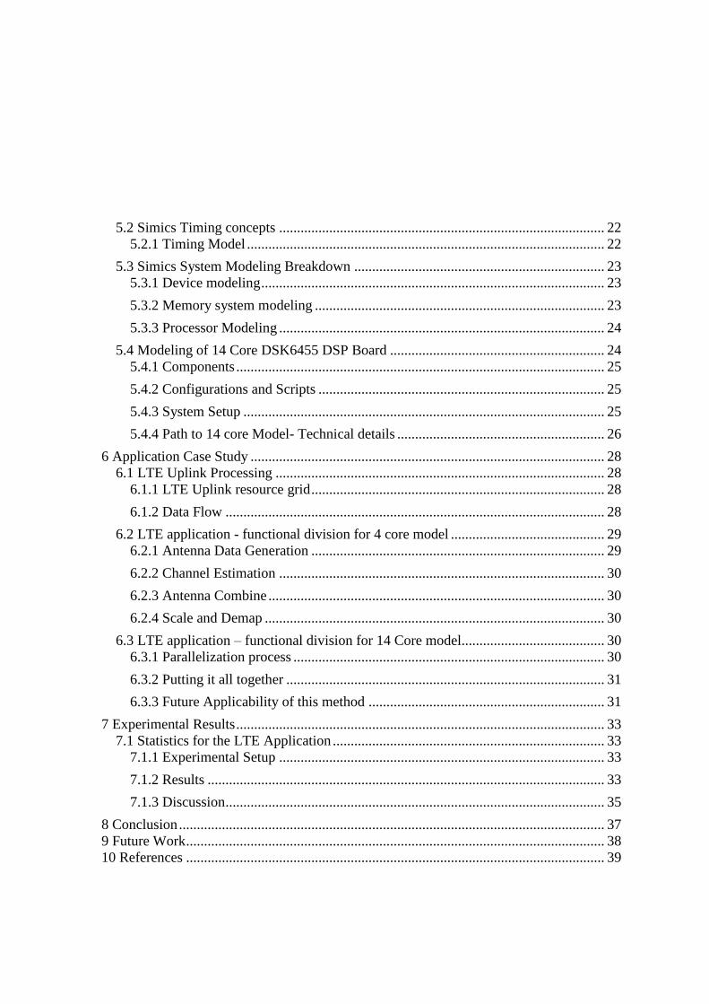
LTE is considered to be the first step towards 4G. 4G actually defines a standard set of
requirements to meet future demands of mobile phone networks. Primarily these requirements
are set in response to current trends in the cellular industry. For example packet data traffic
has surpassed voice traffic since summer of 2007 (see Figure 1) and since last two years there
is exponential growth in data traffic as compared to voice traffic. This was mainly due to the
introduction of HSPA which improved the end user experience. It increased the downlink
speed up to 14 Mbps and uplink speed up to 5.4 Mbps and this increased bandwidth enabled
the users to surf the web efficiently as well as in a limited way to enjoy real time contents like
online audio and video and other multimedia services.
The other major indicator reflecting the increased demand of packet data is mobile broadband.
Broadband subscriptions are projected to reach 3.4 billion in 2014 and 80% of it will be
mobile broadband (see Figure
3). Anticipating these trends,
4G working group put forth
objectives for new generation
(4G) of mobile networks. The
requirements related to
bandwidth included high
network capacity, spectral
efficiency, data rate of 100
Mbps for a moving client and
1 Gbps for a static one and
lower latency. LTE even in its
current form happen to meet
most of these requirements
and even surpass a few as well.
2.2 Standardization
The first step towards LTE standardization was taken in Toronto, Canada in 2004 at 3GPP
RAN Evolution workshop. The basic idea was to develop a framework for the progress of
3GPP radio network technology that could facilitate cheap cost per bit, adaptation of new and
existing frequency bands, a simple architecture that could allow seamless integration with
existing standards and which could enable mobile terminals to consume less power.
Figure 2: LTE standardization process
Figure 1: Trends in voice and data traffic Source: [2]

Current version of LTE represents improvements in Universal Mobile Telecommunications
System (UMTS) which will be introduced in 3rd Generation Partnership Project (3GPP)
Release 8 [7].
The original LTE requirements envisioned by 3GPP included
100 Mbps downlink and 50 Mbps uplink
Reduce the Radio Access Network (RAN) time to less than 10 milliseconds (roundtrip
time for complete LTE frame).
Improved spectral efficiency as compared to HSPA release 6
Also LTE should be able to
incorporate IP connectivity
with improved broadcasting
and flexible bandwidth
allocation schemes.
It should also support
internetworking with existing
3G and networks not
compliant with 3GPP
standard.
The specification work for
LTE completed in March
2009 (see Figure 2) and it is
ensured that implementation
based on 2009 specifications will meet backward compatibility.
2.3 Architecture and Technicalities
In the network world there was a constant effort to develop a common standard protocol
which could serve as middleware for various existing network protocols. The introduction and
success of internet has made packet based IP protocol as the universal standard. Realizing this
3GPP in 2004 proposed IP as the protocol for next generation of its networks. This
recommendation of a new architecture is a part of the 3GPP System Architecture Evolution
(SAE). LTE-SAE is designed to incorporate and support huge market share of IP-based
services.
LTE uses OFDM (Orthogonal frequency division multiplexing) for both uplink and downlink.
OFDM is chosen as the radio technology because it meets the LTE requirements for spectrum
flexibility and wide carriers for peak data rates. However the standard version of OFDM has
high Peak to Average Power Ratio (PAPR). Which means that in order to manage PAPR in
the mobile terminal, you have to use expensive power amplifiers that would increase cost of
the terminal and also would drains its battery faster. Therefore uplink uses a pre-coded
version of OFDM called SC-FDMA which addresses these issues.
To achieve peak data rates and extended coverage that meets the future broadband
requirements another enhancement that LTE borrows from HSPA is advanced antenna
solutions. There are different variants of it based on the arising situation. For example
extended coverage is supported using beam forming and peak data rates are achieved using
MIMO technology that employs multiple input and output antennas.
Figure 3: Projected broadband growth 2007-2014 Source: [2]

3 Overview of Multi-cores
3.1 Background In recent past, for almost a decade, the most popular approach to gain computational
performance was to increase the clock rate or to devise new strategies for exploiting ILP
(instruction level parallelism). As a result every new enhancement to get more ILP made the
architecture more complex, consuming much more power. Both these approaches have
exhausted because of diminishing returns and issues of high power consumption and
dissipation.
Now the fact that clock rate can not be increased beyond a certain limit due to power
dissipation (see Figure 4), the only way forward, one may imagine at this point in time, is to
increase the number of cores and hope that software, which is predominantly sequential in
nature, will be parallelized to
take advantage of this
increased performance,
offered by these multiple
cores on chip.
Parallelism promises same or
higher performance at lower
clock rates (as work can be
done in parallel). Lower clock
rate means lesser power
consumption.
3.2 Multi-cores and
signal processing (LTE
application)
Fortunately, most of the
signal-processing applications
are parallel in nature (signal
processing applications are
extensively SIMD (Single
Instruction Multiple Data)
because it deals most of the time with matrix and vector data which may be processed
independently), this factor also tempts to yearn for parallelism at coarse grained (thread) level
rather than instruction level. Therefore signal processing applications can immensely benefit
from multi-core architectures.
It is argued that the design of multi-cores for such applications should be simpler (due to
predictable execution loops there will be less complicated issues of cache coherence, dynamic
prediction and synchronization etc) as compared to general purpose multi-cores and this fact
is verified during this thesis work as well. For example in the process of parallelizing the LTE
application code to make it run on 14 cores, I was able to identify parts of the application, that
could be done in parallel, by simply inspecting the code.
3.3 Why Texas Instrument®?
The selection of TI® as the DSP vendor for this thesis work is done after performing various
case studies on existing multi-core DSPs commercially available in the market. There are lots
Figure 4: Power dissipation w.r.t. clock rate

of factors contributing to the worth of a multi-core DSP however we selected and focused our
attention on areas that are potentially critical for the existence of any DSP solution in the
foreseeable future. These include scalability, software model, development support, multi-
threading and power consumption.
After much consideration, TI’s solution is selected primarily because it’s famous
TMS320C64x+™ DSP core is available for experimentation in virtual form. Virtutech® [6]
has developed its virtual model in Simics™ [6]. This model has good signal processing
capabilities and is available to academia for experimentation. This virtualized model has
opened a whole new range of possibilities for software developers. Simics will be explained,
in detail, in the following chapters.
The major DSPs studied are Freescale™ semiconductor MSC8156, TILERA® TILEPro64
and Texas Instruments®
TMS320C6455. I will now briefly discuss architecture of TI’s DSPs
in terms of their future scalability and will also touch upon Freescale® and TILERA® DSPs.
Some of the salient features of these DSPs may be found in Table1.
3.4 Texas Instruments This thesis work is based on Texas Instruments® TMS320C6455 DSP. The actual case study
was done for TI’s latest commercial DSP, TMS320TCI6487. However these devices are very
similar. The most important factor is that both these DSPs use the famous TMS320C64x+™
CPU core for which Virtutech® has developed the virtualized processor. Also both these
DSPs have same mix of peripherals and on chip memories. The main difference is that
TCI6487 has three C64x+™ DSP cores (c6455 has one), a faster DDR2 memory and new
antenna support. Nonetheless for the purpose of this thesis work, architecturally both these
DSPs are the same.
First I will briefly explain the architecture of TMS320C6455 DSP and C64x+™ CPU core,
after that will discuss the findings about TMS320TCI6487 DSP.
3.4.1 TMS320C6455
This DSP is based on advanced VelociTI™, very-long-instruction-word (VLIW) architecture
developed by TI®, targeting video, telecom and Wireless infrastructures. It has performance
of 9600 MIPS (million instructions per second) operating at a clock rate of 1.2 GHz and 90nm
process technology is used in fabrication. Power dissipation is 3.3W and performance per
Watt is 2.9 MIPS/mW.
TMS320C6455 device has
2Mbyte L2 memory and 32
Kbyte level1 program
(L1P) and data (L1D)
memories (see Figure 5).
L1D is two way set
associative cache where is
L1P is direct mapped. L2
memory may be used as 4-
way set associative cache
or configured as SRAM.
3.4.2 C64x+ CPU core
C64x+ CPU comprises of
eight functional units, two
register files and two data
paths (see Figure 6). Since Figure 5: TMS320C6455 DSP block diagram

signal processing applications are math intensive therefore C64x+ incorporates special
instruction set enhancements for multiplication and arithmetic logic
operations like 32bit multiply, complex multiplication and parallel add and subtract.
3.4.3 TMS320TCI6487
TCI6487 is one of TI’s latest commercial DSP specifically targeting wireless infrastructure
applications. Therefore I have looked at its multi-core architecture critically.
3.4.4 TCI6487 Case study
Operating System There is no sophisticated operating system present (like Linux® kernel 2.6) which may
leverage multiple concurrent task management (using scheduling techniques like priority
scheduling, time sliced scheduling etc). However it supports DSP/BIOS, a RTOS (Real Time
Operating System) but this RTOS has limitations e.g. it supports only priority scheduling
based on software interrupts and tasks, which means that some low priority tasks might starve
and there could be “priority inversion” issues. The advantage of an RTOS is that DSP/BIOS
allows direct access to manipulate hardware resources (which is not possible to that extent in
Linux since it maintains strict separation between user application and physical resources, so
if a user space program accesses a device an expensive context switch to kernel mode is
required) e.g. hardware interrupts which gives more fine grained control to reduce system
latency. To address these issues related to both GPOS(General purpose OS) and RTOS a third
party supplier Virtual Logix® has tried to come up with a hybrid solution, namely VLX (a
virtualizer), enabling a Linux based development environment to run alongside TI’s
DSP/BIOS.
Architecture and Scalability
Coherency There is no cache coherence protocol implementation (snoopy, directory based etc) between
on chip caches and memory, among the three cores. However for a multi-core solution to
work correctly, shared memory transactions (reads, writes) should meet serializability and
sequential consistency conditions. TCI6487 uses the semaphores module to meet these
conditions[16]. Not only it manages resource sharing but also helps in keeping cache
coherency between the three cores. A multi-core shared memory semaphore implementation
(for cache coherency) requires two main ingredients, one, hardware should support atomic
read-modify-write operations (e.g. test and set, test test and set etc) and, two, these operations
should be non interruptible (similar to single processor implementation to maintain sequential
consistency). But this two fold semaphore solution comes at a price, e.g. a resource (e.g.
SRIO®) can not be shared between two cores at the same time, one has to wait for the
resource until it receives the signal from the other (core) to go ahead.
Architecture scalability Literally three C64x+ cores are placed side by side on one chip. One reason could be that
multi-cores in embedded industry are still at an early stage. But in the wake of dozens, if not
hundreds, of cores on chip in the near future, an operating system similar to Linux is dearly
required which could support multithreading, manage load balancing, load sharing and switch
off idle chips etc. However currently according to TI [13], they have intentionally kept it
generic so that third parties could come up with innovative ideas and solutions.

Expensive (in terms of CPU cycle consumption) semaphore signaling means there will be
issues related to synchronization and latency because of resources blocking. Also I think this
approach is not scalable from futuristic point of view as well, even by adding a few more
cores, the complexity of its architecture will greatly increase. However current DSP solutions
has cores in single digit and there are no critical issues of load balancing or scheduling. This
is partly due to extensive SIMD nature of signal processing applications.
With a weakness in multi-cores, TI is focusing more on functional integration, that is,
defining TCI6487 scalability in terms of number of chips that can be connected together
seamlessly using for example SRIO daisy chain network which uses hardware packet
forwarding to advance data to a specific DSP in the daisy chain, however message passing is
always expensive and a serious performance bottleneck. Based on requirements they have
proposed a so called system-on-chip architecture if there is no task dependency among chips
and each DSP is doing the same functions and other architecture called customized
architecture if role of each DSP is
different from each other.
3.5 TILERA TILERA’s TILEPro64™
processor targets the embedded
market. It has an impressive 64
processor cores connected to each
other through its iMesh™
network. Each processor has L1
and L2 cache and a non blocking
connection to the iMesh™. It
incorporates its trade mark
dynamic distributed cache
(employs concept of
“neighborhood caching”, so in
case of miss a processor may
consult remote processor’s sub-
cache) which claims to be twice
as fast compared to other multi-
cores. Also each processor tile can run independent operating system or multiple tiles may be
combined together to form SMP Linux like OS. Each processor support 32bit VLIW
architecture and is capable of handling up to 3 instructions per cycle.
3.6 Freescale semiconductor The latest Freescale DSPs aimed at wireless base stations is MSC8156, it has 6 cores
(StarCore SC3850) operating at 1GHz, a built in Multi Accelerator Platform Engine for
Baseband (MAPLE-B) and various other features to optimize it for 3G-LTE, 3GPP, TD-
SCDMA etc. It’s an enhanced version of previous chip combo of MSC8144/MSBA8100 that
Freescale® launched in the middle of 2008. MSC8144 is a quad core (SC3400) DSP chip that
works with MSBA8100 chip which is a baseband accelerator. It has 32 Kbyte L1 instruction
and data cache available on each core. Also it includes 512 Kbyte L2 cache which may be
used for both instruction and data along with 1056 Kbyte shared M3.
Figure 6: C64x+ CPU Core, block diagram

Table 1: DSP comparisons
Vendor DSP
# of Cores
/
Frequency
Power
CMO
S
Tech.
Languag
e support
System
Simulator
Freescale® MSC8156 6 / 1GHz 10 W 45 nm
C, C++
compiler
yes
TI® TMS320T
CI6487 3 / 1GHz 6 W 65 nm
C, C++
compiler N/A
TILERA® 64 / 866
MHz 23 W 65 nm
C, C++
compiler yes
Vendor DSP Throughput Development
tool
Operating
System
Support
Freescale® MSC8156
48000
MMACS
CodeWarrior
v10 SmartDSP
TI® TMS320T
CI6487
24,800
MMACS
(16-bit)
Code Composer
Studio DSP/BIOS
TILERA® TILEPro64
Max. of 443
billion
operations
per second
MDE
SMP Linux
with 2.6
kernel

4 Instruction Set Simulation
4.1 Background Simulations are used to recreate an environment for the real system in enough detail, so that
the desired effects can be observed [8]. Simulators therefore eliminate the need of actual
hardware unavailability or shortage, which is most of the time a major bottleneck for software
developers.
4.1.1 Why Instruction set Simulators?
When one talks about simulators the next obvious question is do you need an accurate
simulation or exact numbers? Or you need fast simulation speed for functional verification of
your software application? Before answering these questions lets see how simulators actually
work.
There are two broad categories of simulators
1) Timing/cycle accurate simulators
2) Instruction set simulators
4.1.2 Timing Accurate simulators
Timing accurate simulators works in cycle (timing) accuracy and provides very high visibility
into processor and applications. In this mode, in order to model detailed operations like bit
reset and register access etc. a lot of computation power is required therefore this mode is
very slow and running of only core algorithms in this mode are recommended.
4.1.3 Instruction set simulators (ISS)
Instruction set simulators simulates the target processor at instruction set level. These
simulators are detailed enough to run the executable programs written for the intended target
machine.
Advantages The biggest advantage of instruction set simulators is that they can be used to execute
applications for computers that, for various reasons, do not exist. Another major advantage is
that they can be used to view the internal state of the system which in case of real hardware is
not possible. Also with the introduction of multi-cores and multiprocessors, heisenbugs have
started to occur more frequently, instruction set simulators help in this regard as well. You
will always get the same output no matter how many times you re-execute the program in a
multi-core or multiprocessor. Therefore complete control of the system to track changes at
instruction level can provide comprehensive insight about the behavior of the applications
which may be used to address issues spanning all areas of multi-cores(mainly three), that is,
compiler, architecture and application.
Aim of ISS (Instruction set simulators) Instruction set simulator is used to check functional correctness of the application and bring
the code to life. Since they are not intended to get actual real data/values therefore a lot of
tricks and workarounds are done to simulate the actual behavior of the system. These
shortcuts lower the simulation workload enormously that’s why they are very fast as
compared to cycle accurate simulators. Even these are capable of simulating multiprocessors
systems at satisfactory speed and accuracy.
One such simulator is Simics, which is a System-level Instruction Set Simulator.

4.2 Introduction to Simics Simics is a virtualized software development platform developed by Virtutech
® [6]. It
provides the hardware and software developers with the virtual version of their target
hardware and is capable of running from a single CPU with local memories to a complex
system on chip (SOC) at good speeds. At the same time debugging and testing is simplified
with the help of check points, determinism and reverse execution.
4.2.1 VSD (Virtualized software development)
Background Moore’s law still holds, now in form of multi-cores, therefore with increase of the transistors
complexity of the electronics systems is increasing every day. Also if we take the example of
mobile phones, now a day the other factor increasing the complexity of the system is that
devices communicate with their environment frequently. For example a mobile phone device
through Bluetooth™ and Wi-Fi™ interacts with its surroundings.
These two trends have in turn made the software increasingly complex. Now considering
these obstacles if the target hardware is in short supply or it does not exist then it’s a
nightmare for software developers. One option is to test software on something that some
what at least approximates the production hardware. In the wake of an evolving application
and the hardware that does not exist both these approaches are un-reliable thus not practical.
Solution VSD (Virtualized Software Development) Simics jumps in here with its so called VSD solution (see Figure 7) that combines the speed
and accuracy of software development to the desktop PC. Virtualized software development is
a way of developing software with out the need of actual target hardware, on which the
software will eventually run. VSD allows the software developers to use target hardware on
their own workstations.
Since VSD allows running the exact same binary that would run on physical hardware
therefore it eliminates the need to use stubbed software or API abstraction layers for two
different environments e.g. production environment and test lab environment.
To accomplish above mentioned goals VSD takes care of following four areas
1. Provides an instruction set simulator for the microprocessors in the target hardware
2. Provides device models (simulating the behavior of devices) in the target hardware
that the software might interact with
3. Takes care of interaction, if any, among multiple simulated targets or outside
world(e.g. networks, firewall etc)
4. Allows the software developer to use all the tools that he might use with actual
physical target
Electronic design automation (EDA) industry also provides simulation tools for software
development which are very accurate as well but they take enormous time to execute the
software. VSD is valuable in this regard as well since it gives real time simulation speed.

Figure 7: Traditional vs. Virtualized software development
4.3 Simics - software development concepts
Simics is a system level instruction set simulator which means that
Simics can model the target system at instruction level (executing them one by one)
and
Simics interface for application binaries to the virtual hardware model is so accurate
that it can execute the same binaries that run on real hardware.
This essentially means that Simics is capable of running and debugging almost any kind of
software, firmware, hardware drivers and operating systems.
4.3.1 Simulation limits
However one should take care of a few things while developing software in Simics. The
model of time in Simics is pretty trivial; it assumes that all the instructions take same amount
of time to execute. There might be some issues in multiprocessor environments where certain
assumptions are made about delayed inputs or outputs, however this is not an issue majority
of the times. Also the model of the target hardware should be detailed enough so that while
running, software should not detect any difference between real and virtual hardware.
4.3.2 Simics debugging capabilities
For any software application, speedy development and quick time to market is directly
proportional to the debugging capabilities of its development environment.
Simulation time and debugging One of the biggest advantages of full system simulation is that time in the simulation is
completely independent of the real world time. This gives a number of advantages for
example
One can pause and view the state of system at any point which is almost impossible in
real hardware
State of the system can be saved into disk (checkpoint) and may be restored later
No heisenbugs, complete determinism
Reverse execution, very handy to find elusive bugs
Debugging The most powerful tools for debugging in Simics include
1. Breakpoint support

2. Scriptable debug and symbol information handling
Breakpoints Breakpoint in Simics can be set on code as well as data e.g. they can be set on memory
accesses, time, instruction types, device accesses and output on the console.
Symbolic Debugging The breakpoints set at bits and bytes level are not always meaningful and required. Debugger
should enable the user to think at higher level as well i.e. in terms of functions, processes and
named variables.
Simics implements this using certain classes namely context, symtable and process trackers.
These concepts are critical in order to simulate multi-cores in Simics.
Context A context object symbolizes a virtual address space which is assigned to a processor in multi-
core simulation. If the context is selected for a processor, this address space is visible to the
code running on the processor. Similarly virtual breakpoints can be assigned to a virtual
address space. In a multi-core environment, context objects are very useful for debugging and
measurements e.g. during simulation if you want to inspect code running on a certain
processor, you can select that processor using “pselect” and set breakpoint in its context. So it
allows you to maintain separate debugging symbols and breakpoints for separate processors in
the target machine.
However context object does not in any way effect correctness of simulation, they are just
used to understand the software.
Symtable Symtable objects are used to store information about symbols and debugging for a certain
virtual address space. Symtables are associated with context objects and are used by Simics to
switch between code addresses, variable names and memory locations.
Symbolic Breakpoints In this thesis work symbolic breakpoints along with haps are extensively used to extract
profiling data from simulation and thereby used for performance measurements.
Following statement tells how to read symbolic information from a binary file.
new-symtable st0 file = my_file
Here symbolic information is read from binary file “my_file” and stored in a new symtable
named “st0”.

5 Modeling in Simics
This section starts with a brief description of the modeling process in Simics. After that it
explains how different components of system are modeled in Simics. Finally it elaborates how
to setup different machine configurations using scripts and how starting from a single core
DSK6455 board I created its 14 core model.
5.1 Simics Modeling Process
For developing a virtual system in Simics, there is a generic out line
Create list of devices, processors etc that constitute the system
Decide level of abstraction according to requirements
Reuse if device models already exist, use the device modeling language(DML) to
create the remaining devices
Test the newly created system with the intended software and iteratively compensate
and improve the model to desired levels
The key in development is to get the working prototype early no matter how trivial it is and
iteratively enhance its functionality.
5.2 Simics Timing concepts Simics simulates the behavior of the system and does not implement actual physical
phenomena. Simics simulation model does not model the actual details of how bits or bytes
are transferred across interconnect, instead it can be considered as one possible
implementation of the target architecture. For example, in a real physical system, a processor
requests bus access in order to write to a memory location but in Simics reads and writes are
directly routed to target memories without involving any buses. To make the virtual target
work like the physical one, Simics employs certain proprietary tricks and techniques.
5.2.1 Timing Model
One of the major differences that can exist between real hardware and Simics simulation
model is timing. This difference could be due to number of reasons e.g. incomplete
documentation, desire to increase simulation speed etc. The most significant timing difference
between real and Simics model is observed in instruction execution timings. For example in
real hardware instruction timing depends upon memory access latencies, bus contention etc
whereas in Simics, by default, each instruction takes exactly one cycle to finish. However in
order to simulate actual behavior, it is possible to build timing accurate models and connect
them to Simics.
In Simics, completion of one simulation instruction is also called execution of one step.
Instruction Execution Timings
In-order mode In default mode, Simics executes one instruction in one cycle. It does not model actual
execution timing in any way. So in this case number of cycles equals the number of
instructions.
Stalling mode If the goal of simulation is to perform detailed studies, e.g. involving timing of memory
access operations, then Simics functionality of in-order model may be enhanced by adding so

called timing models. This is usually done using memory hierarchy interface (see section
5.3.2). In this mode of simulation, instructions no longer finish atomically but rather stall for a
specified number of cycle events before a step event is executed.
5.3 Simics System Modeling Breakdown
Simics divides the system into three broad categories and models them differently
1. Device modeling
2. Memory system modeling
3. Processor modeling
5.3.1 Device modeling
Device modeling in Simics is implemented using a technique called transaction level
modeling (TLM) which uses Virtutech’s device modeling language(DML) [13]. When a
device is presented with a request it computes the results and replies. As explained above, it
does not bother about bits and bytes, making implementation convenient as well as efficient.
5.3.2 Memory system modeling
Simics has developed a very efficient technique to handle the memory system and processor
bus interface. This technique is instrumental in Simics success of ensuring a very fast
simulation. Processor address space is modeled as a memory map and the target memories
and devices in the system are assigned to that memory space (see Figure 8). So reads and
writes are routed directly to the recipient devices with out involving any buses or bridges.
If system timing requirements are not affected by impact of cache hierarchies and bus access
latencies, then this method often allows the virtual system to perform better, in terms of
speed, than the original system. Please see section 5.2 for timing details.
Memory Spaces Memory accesses in Simics are handled by the generic memory-space class. An object of
class memory-space implements necessary functions for memory accesses and has attributes
specifying how memory mappings are setup for a processor. The most important attribute in
memory-space class is the map attribute which provides a list of mapped objects in a given
memory-space. Those could include devices, RAM, ROM or even other memory-spaces.
The following example from DSK6455 Simics model explains the concept of memory-spaces
and their usage.
For example first statement below creates a memory space object called “phys_mem” and the
2nd
statement maps a RAM object (namely iram) into this memory space object.
self.o.phys_mem = pre_obj('phys_mem', 'memory-space')
self.o.phys_mem.map = [0x00000000, self.o.iram, 0, 0, 0x1000000]
In the following statements, a CPU object is created and this memory-space (phys_mem) is
assigned to it. So now the CPU object (namely cpu) can access this memory (iram) at address
0x00000000.
self.o.cpu = pre_obj('cpu', 'tms320c64plus' + classname_suffix_cpu)
self.o.cpu.physical_memory = self.o.phys_mem

Memory transactions In Simics, both devices and CPUs can initiate memory transactions. ACPU can get the
physical address (from virtual address) after it is translated by MMU whereas device
transaction does not require any translation. The physical address is actually mapped to a
device or memory (RAM, ROM etc) by memory-space and an access to the physical address
is automatically sent to the right target by the memory-space class.
For observing or modifying memory transactions, memory-space class has a special memory
hierarchy interface. This interface in fact consists of timing_model interface (gives access to
transaction before execution) and snoop_memory interface (provides transaction access after
it has been executed)
Figure 8: Simics model of the newly created 14 core DSK6455 DSP board
5.3.3 Processor Modeling
In Simics processor modeling is not done using DML because then simulation of processor
alone would consume all the processing power of the host machine. The processor models are
developed and shipped by Virtutech® and are highly optimized, enabling Simics to simulate
billions of instructions per second.
5.4 Modeling of 14 Core DSK6455 DSP Board This section explains how different elements of Simics are put together to create a working
virtual model of a target physical system. At the same time DSK6455 model is related to
these details where possible.
Simics model is designed in bottom-up fashion, first of all devices are created which are
combined to form components. Finally a complete system is constructed in Simics, using
configuration scripts (see Figure 9).

5.4.1 Components
Any standalone piece of hardware that can be connected or removed from the system is
represented by a component in Simics. A component is basically a collection of devices which
are connected together though different interfaces. Components have various types of
standard connectors in order to connect to interfaces like Ethernet and buses. Components
hide complexity of the system and give an easy to understand overview of the system from
outside. It is implemented by a component module which is placed in the workspace
directory.
Components are written in “python™”. DSK6455 component is named
“dsk6455_components.py”.
5.4.2 Configurations and Scripts
Most convenient way of starting Simics is through configurations using scripts.
Configurations actually define different components and objects and tell how they are
interconnected. So scripts can be considered at a higher level of abstraction, above
components.
Figure 9: Simics model, hierarchal build up
5.4.3 System Setup
To setup machines and systems in Simics, a configuration consists of many scripts. However
for each configuration there should be at least three kind of scripts.
<machine>-common.simics
This script actually defines the complete
simulated machine. This script file uses
“–system.include” to define hardware and “-setup.include” to define the software of
the system. However since DSK6455 is an embedded system and there is no operating
system present therefore our configuration does not have any “-setup.include” script
file. So “-common.simics” script incorporates this functionality as well.
In our configuration “-common.simics” script is named “himalaya-selftest.Simics”.
<architecture-variant>-system.include
This script defines the hardware of the system.
In our case this script is called “himalaya-system.include”.
<machine>-setup.include
Figure 10: Simics model, hierarchal build up

It defines the software for the system. In our case this script is part of the
common.simics script.
5.4.4 Path to 14 core Model- Technical details
Initially the aim of this work was to create a 16 core model however the LTE application
dictated that a 14 core model will be the optimal one (will be explained in section 5). Since no
new devices were required in order to scale the model from single core to 14 cores therefore I
conveniently skipped to the last part of Simics model development process. I used the existing
devices and modified the Simics model at component level.
4 Core Model The given LTE application consists of 4 major parts therefore the obvious first step, towards a
14 core DSK6455 DSP, was to first create a 4 core model. This model not only provides a
standalone DSP solution, running all parts of LTE application on a single board, but also
serves as a guideline for creating the 14 core model. The process of creating 4 core and 14
core model in Simics is exactly the same. So in Simics one may create as many cores as one
likes, as long as the software can handle it.
The given single core Simics
model consisted of a single
component (dsk6455) which
represents a Texas Instruments
DSK6455 board. This board has
one (C64x+) CPU core. I
modified this piece of hardware
(represented by dsk6455
component class in Simics) and
added 3 more CPU objects in it.
For each CPU a separate
memory-space object is created
and all the devices on board are
mapped into it. Please see section
5.3.2 for an example.
All the CPUs in the new 4 core DSK6455 model share the same address space on board (see
Figure 10). All I/O devices and memories are shared among all CPUs. However for smooth
functioning of this multi-core model, synchronization and mutual exclusion is maintained
through the application software. For mutual exclusion semaphores are used which make sure
that different CPUs do not step on each other’s feet. The application programs assigned to
each CPU core are loaded into a pre-allocated area in the internal on chip memory (namely
iram). This particular memory section is local to every CPU core and no other processor can
access it. The rest of the iram is shared and is available to every CPU, so it may be called as
the working area for all (4 or 14) cores on board. Here with the help of synchronization
primitives, output from one CPU core may be used by the other one as input. For example
“Antenna_Combine” part of the LTE application uses the result from “Channel_Estimates”
part as input operating in the same shared memory.
Figure 11: 4 cores Simics model of DSK6455

14 core model The construction of the 14 core model in Simics is the same story as 4 core model. Here I
created 14 CPU objects instead of 4, as in previous case and repeated all the steps mentioned
in section 5.4.4 (see Figure 8).
Therefore creation of a multi-core model in Simics is relatively trivial; the real challenge is to
build a complete working software hardware package that optimally utilizes the full potential
of all cores. For that matter comprehensive understanding of the given software application is
required.

6 Application Case Study
This section starts with a brief introduction to LTE uplink processing. It then explains 4 part
functional division of the LTE uplink processing application. Next it explains how 4 part
application is further divided into 14 functionally independent parts that can be processed
autonomously. In the last part, issues and avenues related to future scalability of this model
e.g. increasing the number of cores, limitations and bottle necks are discussed.
6.1 LTE Uplink Processing For both uplink and downlink LTE uses OFDM as the radio technology. However to
compensate for high peak to average power ratio (PAPR) of OFDM, uplink uses a special pre-
coded version of it, called SC-FDMA. In order to understand LTE uplink processing first
hand knowledge of the uplink physical layer is required.
6.1.1 LTE Uplink resource grid
In the time domain, one uplink slot
is 0.5ms in length and contains 7
OFDM symbols (see Figure 11).
In frequency domain, subcarrier
spacing is 15 kHz. 12 subcarriers
combine to make a resource block
(see Figure 11). Each resource
block has 84 resource elements.
One resource element may contain
different number of bits based on
the modulation scheme. For
example for 64QAM each resource
element will contain 6 bits.
Similarly for 16 QAM modulation
scheme one resource element will
contain 4 bits. Bit rate or bandwidth
for a certain user is directly
proportional to the modulation
scheme used for the resource
elements, the higher the modulation
scheme the more the bandwidth.
6.1.2 Data Flow
Figure 12 shows simplified block
diagram for LTE uplink processing
application. Every 70 microseconds
antennas generate data and a new symbol (1200 complex data) arrives. As described earlier, 7
consecutive symbols are grouped together to form one uplink slot. Data is processed one slot
at a time. Since new data is coming all the time therefore LTE application is required to
process an uplink slot before a new one has arrived or in other words, LTE application has to
finish processing(one uplink slot per user) within 0.5 milliseconds barrier (7 symbols × 70µs
≈ 0.5 ms).
Figure 12: LTE uplink physical resource grid

Out of seven symbols in a slot, fourth symbol is called the reference symbol. This symbol is
used to calculate channel estimates. Channel estimates are required to process the remaining
symbols (6) in the corresponding uplink time slot. This step is identified as “Antenna
Combine” and its output is user symbols which are used in next stage. Finally in the end,
based on the modulation scheme and constellations, values are normalized and demapped to
generate 8 bit soft values.
Figure 13: LTE uplink processing
6.2 LTE application - functional division for 4 core model LTE uplink processing may be divided into 4 major stages (see Figure 13). Therefore based
on this functional division, the given LTE application software has four main parts namely
1. Antenna data Generation (stage 1)
2. Channel estimation (stage 2)
3. Antenna Combine (stage 3)
4. Scale and Demap (stage 4)
Please note these are not the standard names; they simply identify and give understanding of
each stage
6.2.1 Antenna Data Generation
In a real setup, this part will not be required since physical antennas will serve this purpose.
However as we are working in a simulated environment therefore we need a data source that
is generating antenna data all the time (see Figure 13).
It is assumed that there are two antenna data sources. This part of application basically
generates dummy antenna data and fills the data buffers allocated for incoming data symbols.
One OFDM symbol is generated in every iteration of this program. According to LTE
specifications, a physical antenna generates a new symbol every 70µseconds therefore in this
simulated setting, calibrations are done with the help of special loops such that a new symbol

is generated every 70 microseconds. Since each time slot consists of 7 symbols therefore the
buffer values are overwritten after every “0.5 milliseconds (70µs × 7 ≈ 0.5ms).
6.2.2 Channel Estimation
This part of the application waits for the reference symbol (4th) in every slot. Once the
reference symbol is available from both the antennas, it starts to calculate the channel
estimates.
When finished it writes the estimates in the shared memory and stops processing until
reference symbol for the next uplink slot is available. At the same time it triggers next part of
the application to go ahead, see
stage 2 in Figure 13
6.2.3 Antenna Combine
In this stage of uplink
processing data symbols are
available even when channel
estimation is being done but it
has to wait for the results from
2nd
stage in order to process
them. Once channel estimates
are available it processes the
symbols one by one and
generates user symbols which
are used in the next stage to get
soft values. When finished it
triggers the final stage.
6.2.4 Scale and Demap
This is the final stage in uplink processing. It waits for the user symbols from the “Antenna
Combine” stage and converts them to soft 8 bit values which are understandable by
computers.
6.3 LTE application – functional division for 14 Core model The functional division of LTE application into 4 parts was pretty straight forward. Next step
was to further divide the application into parts that may be processed independently, so that
the processing power of the envisioned 16 core DSK6455 DSP, which eventually reduced to
14 cores (see Figure 15), is fully utilized.
6.3.1 Parallelization process
For the sake of parallelizing, I deliberated on last three stages of LTE uplink processing (since
first stage in this model is just meant for simulating antenna behavior).
Parallelism in “Channel Estimate” stage This part of the application basically processes the 4
th symbol or the reference symbol (see
Figure 13) in the uplink slot. A good look at the code reveals that, at macro level, there are no
functionally independent sections. Mainly there are loop carried dependencies therefore to
extract functionally independent parts of this code sophisticated code optimization techniques
like loop unfolding [9], software pipelining [10], DO-ACROSS parallelism [11] and
Sensitivity analysis) [12] may be used.
Figure 14: LTE uplink processing, functional division

Parallelism in “Antenna Combine” stage Antenna combine stage processes the
remaining 6 symbols in the uplink
slot (excluding the reference
symbol). Each of these symbols is
processed independently of each
other, one by one. Since there is no
functional dependence among these
symbols therefore every symbol may
be processed independently of each
other. So instead of processing each symbol one by one, all of them may be processed in
parallel at once. This functional division can straight away reduce the processing time for this
part of the application by a factor of 6. That is exactly what I have done (see Figure 14).
Parallelism in “Scale and Demap” stage This is the final part of the application and its functionality is pretty similar to the previous
“Antenna Combine” stage. It also processes 6 symbols in the corresponding uplink slot, one
by one, generating soft values for each of them. Since there are no dependencies among these
symbols therefore these symbols can be processed in parallel and latency for this stage can be
reduced 6 times as well (see Figure 14).
6.3.2 Putting it all together
After the functional division of last two stages of the LTE application into 6 parts each, now
we have identified 14 functionally independent parts of that application that may be processed
in parallel. So if we use the originally planned 16 core model of DSK6455 DSP, 2 cores of the
chip will be literally sitting idle doing nothing therefore a decision was made to use a 14 core
model instead of 16 cores.
6.3.3 Future Applicability of this method
The method used in dividing this application into 14 independent parts may be extended by
having detailed studies of the actual complete version of the LTE application and by looking
at LTE physical layer specifications in depth.
Using this 14 core application model, one straight forward enhancement could be to a 28 core
hardware model. By introducing a secondary antenna data source on chip, operating at
frequencies other than the previous sources to avoid interference, to feed the newly added 14
cores, if dynamic load sharing can be done, this form of parallelism can reduce hardware and
power costs.
Figure 15: LTE uplink slot

Figure 16: LTE uplink processing 14 core model

7 Experimental Results
The main aim of this thesis work is to study and comprehend the potential of Virtualized
System Development and to use Instructions Set Simulation for creating hardware that does
not exist and then test an application on it that is still evolving. Also LTE application used for
this thesis work does not represent the actual work load therefore it is meaningless to look for
numbers as they can not be compared with actual existing commercial DSPs in real working
environment. Also Instruction Set Simulators make use of certain tricks to simulate the actual
behavior of the physical target hardware therefore it can not be relied upon for precise
calculations.
However in this thesis work, two multi-core models are discussed, 4 cores and 14 cores. The
four core model was built to port all parts (4) of the LTE application on a single board to
make it a stand alone DSP solution. Therefore it is used as a reference point in relation to
further enhancement towards the 14 cores model.
In the rest of this section I will briefly explain the experimental setup used for the
calculations and results related to different parts of the LTE application and over all
performance enhancements from 4 cores to 14 cores model.
7.1 Statistics for the LTE Application
7.1.1 Experimental Setup
CPU Frequency = 1000 MHz
For all the calculations, the codes are compiled in the “Code Composer Studio” at
optimization level zero (0) except “Antenna Generation” part where optimization level 2 is
used.
Antenna Data generation setup Since we need to simulate antenna data to generate a symbol every 70µs therefore operating
at 1000 MHz, every 70000 intervals a new symbol is generated (Simics assumes a perfect
memory model and executes an instruction every new cycle therefore cycle rate =step rate
here).
7.1.2 Results
This part gives details about statistical numbers (number of cycles consumed) in a particular
section of code. Since 0.5millisecond is the time barrier to complete the uplink processing for
one time slot therefore I have chosen it as the reference point for all calculations. Firstly time
for every individual stage of application is calculated then a comparison is made, for complete
application time, between 4 and 14 cores to see if it meets the 0.5millisecond barrier.
Time is calculated in terms of number of cycles (as CPU frequency is 1000MHz therefore
1000 cycles equal one microsecond).
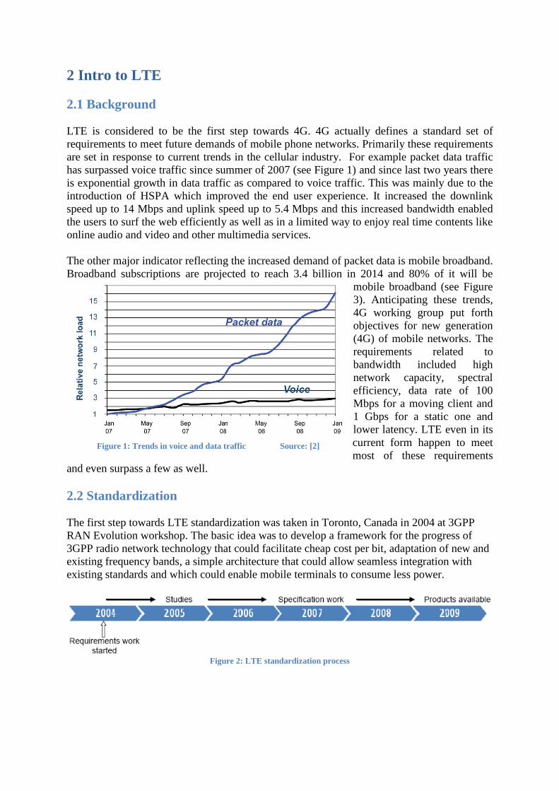
Individual stages Table 2 summarizes the speedup for different stages in the application. Stages “Antenna
Combine” and “Scale and Demap” are divided into 6 parts each whereas “Channel Estimate”
stage remains unchanged.
Table 2: Speedup comparison between Parallel and Sequential execution
Mode of execution
Application Stage
Sequential (Single-core)
Parallel (6 cores)
Cycles
consumed
Time
consumed
(milliseconds)
Cycles
consumed
Time
Consumed
(milliseconds)
Channel Estimate
110227 0.110 n/a n/a
Antenna Combine
916135 0.916 152598 0.152
Scale and Demap
292781 0.292 49223 0.049
Figure 17: Antenna Combine, parallel vs. serial execution
Figure 18: Scale and Demap, parallel vs. serial execution

Complete application time After antenna data is generated, Table 3 shows total time consumed to process one uplink slot
(time consumed by all 3 parts of the application, starting from Channel_Estimate through
Antenna_Combine till Scale_Demap).
Uplink processing for the very first time slot consumes 1.38 milliseconds, after that when data
is in pipeline, processing for one uplink slot, on the average, takes 0.902 milliseconds.
Table 3: Execution time for complete application, 4 vs. 14 cores
Execution Time
Cycles
consumed
Time consumed
(milliseconds)
4 Cores
901970 0.902
14 Cores
410942 0.410
Figure 19: Complete application execution time, 4 vs. 14 cores
7.1.3 Discussion
From hypothetical point of view and for the sake of comparison, in case of 4 core model the
results reveal that if the data is processed in a sequential manner, this implementation of the
application processes one uplink slot in 0.902 milliseconds which breaks the 0.5 milliseconds
barrier. Parallelizing the second and third stage of the application straight away gives an
improvement by a factor of 6 in those stages however 14 cores model completes the

processing in 0.410 milliseconds which meets the time limit but does not reflect a linear
speed up in relation to the amount of hardware added (10 new cores) or the speed up in the 3rd
and 4th
stage (under ideal conditions time consumed for all three stages should be around
0.311milliseconds).
This is because new data from antenna source (stage 1 is the bottleneck) is not available for
processing while the later stages (3 and 4) have finished their processing of previous uplink
slot. Actually antenna source is generating the data every 70 microseconds and measurements
reveal that “Antenna Combine” (3rd
stage) has to wait for the antenna data, on the average, for
33microseconds even when the channel estimates are available. This is almost one half of the
time to generate one uplink symbol. This time may be used to serve another antenna source.

8 Conclusion
Foremost conclusion of this thesis work is that “Virtualized System Development”,
employing “Instruction Set Simulation” technique, accelerates the application development
time because target hardware is available even before it physically exists. This allows the
software development team to begin process of experimentation and development right away
and an early start in development eventually exposes the design flaws in both hardware and
software much earlier in the development cycle of the actual physical product. One example is
how the architecture of LTE application influenced to reduce the originally planned 16 cores
model to 14 cores.
Also VSD enables the development team to focus on their actual goals i.e. a developer
consumes almost 60% of the time in debugging and finding errors in code and these matters
have been even complicated with the introduction of “hiesenbugs” in case of multi-cores.
Now because of deterministic reproducible execution and excellent debugging capabilities,
VSD can reduce this time many folds allowing the developer to spend more time on
development rather than debugging.
Simics as a simulation tool is pretty fast and accurate capable of scaling to hundreds of
multiprocessors and multi-cores (using technologies like JIT, page sharing and multi-
threading). With very good debugging and testing capabilities (deterministic execution, inject
faults seamlessly using scripts, reverse execution, ability to save system state and replay it)
which are critical for multi-core software development in the wake of heisenbugs.
The interaction with the LTE application reveals that there is lot of parallelism available in it
which is evident from the results obtained from the 14 core model. Over all system latency is
reduced almost three fold as compared to 4 core model. The same is true for all signal
processing applications. In essence, using virtualized system development, detailed studies of
the LTE application promises to reveal number of avenues leading to a rapid cost effective
multi-core solution that spans dozens of cores.

9 Future Work
The success of a “multi-core solution” lies in its ability to divide and do work in parallel. The
14 core model, created during this study, actually represents one way of dividing the uplink
processing into 14 parts. Therefore to further increase the throughput (number of users) one
way is to reduce the latency by further dividing the LTE uplink processing into independent
parts, let’s say 30, and subsequently develop a 30 cores model for it. This requires advanced
and in depth studies focusing on all layers (e.g. PHY, MAC, RLC etc) of the LTE protocol. In
this case, a reduction in latency would mean that more users can share, thus be
accommodated, in a given time slot (since every user needs to be scheduled only after every
0.5 milliseconds).
Figure 20: User shared uplink slot
Another important aspect is that in LTE a lot of intelligent decision making is delegated to the
base station. For example unlike HSPA, in LTE data rate of the terminal (user) is controlled
by NodeB (base station). Also LTE schedules the users based on channel conditions (shared
channel assignment and data rate). Therefore if two users are sharing a channel in time and
frequency domain, one with high data requirements (real time video content) and the other
one with minimal services (just updating it’s live status) then for optimal resource utilization
future base stations would require intelligent Linux® like operating systems, capable of
efficiently utilizing the available resources (using task sharing and load management) by
temporarily taking resources from one user and allocating them to the demanding one.
Now to explore all these possibilities, involving the software and hardware that does not exist,
virtualized software development (Instruction Set Simulation) seems to be the only solution.

10 References
[1] Young Kyun, Kim; Prasad, Ramjee (2006). 4G Roadmap and Emerging
Communication Technologies. Artech House 2006. pp. 12–13. ISBN 1-58053-
931-9
[2] LTE–an introduction,
www.ericsson.com/technology/whitepapers/lte_overview.pdf date visited 26th
November 2009
[3] LTE (Long Term Evolution), first 4G wireless communication systems
[4] Faroughi, N. 2005. Profiling of parallel processing programs on shared memory
multiprocessors using Simics. SIGARCH Comput. Archit. News 33, 5 (Dec.
2005), 51-56
[5] www.ti.com, date visited 15th
March 2009
[6] http://www.virtutech.com, date visited 25th
March 2009
[7] http://en.wikipedia.org/wiki/3GPP_Long_Term_Evolution
[8] http://www.xsim.com/bib/index1.d/Index.html#Overview , date visited 20th
October 2009
[9] S. Ha and H. Kim. Ku-loop scheme: An efficient loop unfolding scheme for
multithreaded computation. Journal of Information Science and Engineering,
14(1):223–236, 1998.
[10] B. R. Rau and C. D. Glaeser. Some scheduling techniques and an easily
schedulable horizontal architecture for high performance scientific computing.
In MICRO 14: Proceedings of the 14th annual workshop on Microprogramming,
pages 183–198, Piscataway, NJ, USA, 1981. IEEE Press.
[11] R. Cytron. Doacross: Beyond vectorization for multiprocessors. In Int’l Conf.
Parallel Processing (ICPP), pages 836–845, 1986.
[12] Rus, S., Pennings, M., and Rauchwerger, L. 2007. Sensitivity analysis for
automatic parallelization on multi-cores. In Proceedings of the 21st Annual
international Conference on Supercomputing (Seattle, Washington, June 17 -
21, 2007).
[13] http://focus.ti.com/lit/an/sprab24/sprab24.pdf, Page 4, date visited 4th
November 2009
[14] “Modeling your system in Simics” v.4
[15] http://www.mobileshop.com/blog/mobile-phone-news/he-shoots-he-scores-new-
software-to-revolutionise-football-coverage-on-mobile-phones/ , date visited 3rd
November 2009
[16] http://focus.ti.com/lit/an/sprab24/sprab24.pdf, Page 4 , date visited 15th
November 2009


![ECE-V-DIGITAL SIGNAL PROCESSING [10EC52] …vtusolution.in/.../digital-signal-processing-10ec52.pdfDigital vtusolution.in Signal Processing 10EC52 TEXT BOOK: 1. DIGITAL SIGNAL PROCESSING](https://static.fdocuments.net/doc/165x107/5afe42bb7f8b9a256b8ccd2e/ece-v-digital-signal-processing-10ec52-signal-processing-10ec52-text-book.jpg)