Mr. SQUID User's Guide - STAR Cryoelectronics · Mr. SQUID User’s Guide . STAR Cryoelectronics,...
103
Mr. SQUID ® User's Guide Version 6.6 STAR Cryoelectronics, LLC 25 Bisbee Court, Suite A Santa Fe, NM 87508 U. S. A.
Transcript of Mr. SQUID User's Guide - STAR Cryoelectronics · Mr. SQUID User’s Guide . STAR Cryoelectronics,...
Mr. SQUID® User's Guide
Version 6.6
STAR Cryoelectronics, LLC 25 Bisbee Court, Suite A
Santa Fe, NM 87508 U. S. A.

ii
iii
Mr. SQUID® User's Guide
Manual written by Randy W. Simon, Michael J. Burns, Mark S. Colclough,
Greg Zaharchuk, and Robin Cantor
Advanced Experiments written by Michael J. Burns (Exp. 1-5) and
Greg Zaharchuk (Exp. 6)
Mr. SQUID® is a registered trademark of STAR Cryoelectronics, LLC
Copyright © 1996 – 2012
STAR Cryoelectronics, LLC
Mr. SQUID User’s Guide
STAR Cryoelectronics, LLC iv
TABLE OF CONTENTS Technical Support .......................................................................................................................... vi
Warranty ....................................................................................................................................... vii
Safety Precautions ......................................................................................................................... vii
1 Introduction ..................................................................................................................... 1
2 The Mr. SQUID® System ............................................................................................... 5
2.1 System Components........................................................................................................ 5
2.2 Additional Equipment Required ..................................................................................... 5
3 Getting Started with Mr. SQUID® (New Users) ............................................................. 6
3.1 Setting Up the Mr. SQUID® System............................................................................... 6
3.2 Cooling the Mr. SQUID® Probe ..................................................................................... 8
3.3 Varying the Current Offset ............................................................................................. 9
3.4 Varying the Amplitude of the Sweep Output ................................................................. 9
3.5 Calculating the Current and Voltage............................................................................... 9
3.6 Observing V-Ι Characteristics using Mr. SQUID® ....................................................... 10
3.7 Observing V-Φ Characteristics using Mr. SQUID® ..................................................... 15
3.8 Additional SQUID Measurements ................................................................................ 18
3.9 Summary of Basic Experiments.................................................................................... 20
4 Getting Started with Mr. SQUID® (Advanced Users) .................................................. 22
4.1 Electronics Box Front Panel ......................................................................................... 22
4.2 Electronics Box Rear Panel .......................................................................................... 24
4.3 Observing V-Ι Characteristics using Mr. SQUID® (Advanced Users) ......................... 25
4.4 Observing V-Φ Characteristics using Mr. SQUID® (Advanced Users) ....................... 27
5 An Introduction to Superconductivity and SQUIDs ..................................................... 29
5.1 A Capsule History of Superconductivity ...................................................................... 29
5.2 Superconductivity: A Quantum Mechanical Phenomenon .......................................... 29
5.3 The Superconducting State ........................................................................................... 29
5.4 The Quantum of Flux .................................................................................................... 30
5.5 Superconducting Rings ................................................................................................. 31
5.6 Josephson Junctions ...................................................................................................... 32
5.7 The DC SQUID............................................................................................................. 33
5.8 Details of DC SQUID Operation .................................................................................. 34
Mr. SQUID User’s Guide
STAR Cryoelectronics, LLC v
5.9 SQUID Parameters........................................................................................................ 39
5.10 SQUID Operation ......................................................................................................... 41
5.11 Practical SQUID Magnetometers ................................................................................. 42
5.12 SQUID Applications ..................................................................................................... 44
5.13 A Brief History of SQUIDs .......................................................................................... 45
5.14 The SQUID in Mr. SQUID® ......................................................................................... 46
6 Troubleshooting and Getting Help ............................................................................... 49
6.1 Problems in V-I Mode ................................................................................................... 50
6.2 Problems in V-Φ Mode (Assuming Everything Works in V-I Mode) .......................... 51
6.3 Magnetic Flux Trapping in SQUIDs............................................................................. 51
6.4 Degaussing the Magnetic Shield ................................................................................... 52
6.5 RF Interference ............................................................................................................. 53
6.6 Customer Service .......................................................................................................... 55
7 Advanced Experiments ................................................................................................. 56
7.1 Resistance vs. Temperature of the YBCO SQUID ....................................................... 57
7.2 Building an Analog Flux-Locked Loop ........................................................................ 64
7.3 Using a Flux-Locked Loop as a Sensitive Voltmeter ................................................... 68
7.4 The AC Josephson Effect: Microwave-Induced (Shapiro) Steps at 77K and Determining h/e. ........................................................................................................... 72
7.5 Inductive Measurement of the Superconducting Transition Temperature of an HTS Film ............................................................................................................................... 78
7.6 SQUID Properties in Pumped Liquid Nitrogen ............................................................ 85
8 About STAR Cryoelectronics ....................................................................................... 89
9 Technical Specifications ............................................................................................... 90
9.1 Electronics..................................................................................................................... 90
9.2 Probe ............................................................................................................................. 90
9.3 Magnetic Shield ............................................................................................................ 90
9.4 RF Filter Module........................................................................................................... 91
9.5 Cable ............................................................................................................................. 91
9.6 Dewar ............................................................................................................................ 91
9.7 Rear Panel I/O Specifications ....................................................................................... 91
10 References ..................................................................................................................... 93
Mr. SQUID User’s Guide
STAR Cryoelectronics, LLC vi
Revision Record
Date Revision Description
July 17, 2000 6.1 STAR Cryoelectronics Release
January 11, 2002 6.1.1 Updated contact information
April 26, 2002 6.2 Updated specifications
May 10, 2002 6.2.1 Updated specifications
August 8, 2003 6.2.2 Updated specifications
September 8, 2007 6.3 Updated Sec. 3, Sec. 5, SQUID specs.
August 17, 2009 6.4 Revised for EB-03 electronics
August 13, 2011 6.5 Added rear panel I/O specifications
Copyright © 2000 – 2011 by STAR Cryoelectronics, LLC, Santa Fe, NM 87508
All rights reserved. No part of this manual may be reproduced, stored in a retrieval system, or transmitted in any form or by any means, electronic, mechanical, photocopying, recording, or otherwise, without prior written permission of STAR Cryoelectronics.
STAR Cryoelectronics reserves the right to change the functions, features, or specifications of its products at any time, without notice.
TECHNICAL SUPPORT
If you have any questions or comments about this product or other products from STAR Cryoelectronics, please contact:
STAR Cryoelectronics
25 Bisbee Court, Suite A Santa Fe, NM 87508
U. S. A.
http://www.starcryo.com/
Technical Support:
Tel.: (505) 424-6454 FAX: (505) 424-8225 Email: [email protected]
Mr. SQUID User’s Guide
STAR Cryoelectronics, LLC vii
WARRANTY
STAR Cryoelectronics Limited Warranty STAR Cryoelectronics warrants this product for a period of twelve (12) months from date of original shipment to the customer. Any part found to be defective in material or workmanship during the warranty period will be repaired or replaced without charge to the owner. Prior to returning the instrument for repair, authorization must be obtained from STAR Cryoelectronics or an authorized STAR Cryoelectronics service agent. All repairs will be warranted for only the unexpired portion of the original warranty, plus the time between receipt of the instrument at STAR Cryoelectronics and its return to the owner.
This warranty is limited to STAR Cryoelectronics products that are purchased directly from STAR Cryoelectronics, its OEM suppliers, or its authorized sales representatives. It does not apply to damage caused by accident, misuse, fire, flood or acts of God, or from failure to properly install, operate, or maintain the product in accordance with the printed instructions provided.
This warranty is in lieu of any other warranties, expressed or implied, including merchantability or fitness for purpose, which are expressly excluded. The owner agrees that STAR Cryoelectronics’ liability with respect to this product shall be as set forth in this warranty, and incidental or consequential damages are expressly excluded.
SAFETY PRECAUTIONS
Do remove product covers or panels except for modifications as specified in this manual.
Do not operate without all covers and panels in place.
Do not attempt to repair, adjust, or modify the instrument, except for modifications as specified in this manual. This could cause nullification of any warranty. For service, return the instrument to STAR Cryoelectronics or any authorized representative.
Do not operate this instrument in a volatile environment, such as in the presence of any flammable gases or fumes.
The liquid nitrogen dewar provided with Mr. SQUID® is accompanied by instructions from the dewar manufacturer. The user is responsible for the observance of the manufacturer’s directions, warnings and restrictions.
Mr. SQUID User’s Guide
STAR Cryoelectronics, LLC viii
Congratulations! You have just purchased the world's first high-temperature superconductive electronic system product: Mr. SQUID®, originally developed by Conductus and now offered exclusively by STAR Cryoelectronics. Contained in the cryogenic probe is a thin-film integrated circuit chip incorporating a high-temperature superconducting quantum interference device (SQUID). This affordable instrument will allow you to observe several of the unique features of superconductivity without the complications of liquid helium cooling and without specialized equipment or facilities. In addition, Mr. SQUID® will allow you to learn about the operation of SQUIDs by following a series of experiments that can be readily performed in undergraduate laboratories.
Mr. SQUID® is a First
• Mr. SQUID® is the first electronic instrument on the market that incorporates high-temperature superconductor (HTS) thin film devices.
• Mr. SQUID® is the first commercial use of liquid nitrogen cooled SQUID technology.
• Mr. SQUID® is the first instrument for the demonstration of the quantum effects of superconductors designed for undergraduate laboratories.
About This Manual Mr. SQUID® is designed to assist in the education of young scientists in training. Every effort has been made to make this manual as readable and accurate as possible. All of the experiments were performed multiple times before their manual sections were written. Considerable effort has been made to make this product and manual as valuable and easy to use as possible. Just as in performing cutting edge research, however, difficulties performing the experiments in this manual can arise and the apparatus may become uncooperative. We encourage you to contact us if you encounter problems that appear to be insurmountable, or to make suggestions or to point out errors so that we may improve this product and this manual. The best way to contact us is by email at [email protected]. Other means of contacting us about this product are described in the troubleshooting section of this manual.

Mr. SQUID User’s Guide
STAR Cryoelectronics, LLC 1
1 INTRODUCTION
What is Mr. SQUID®? Mr. SQUID® is a DC Superconducting QUantum Interference Device (SQUID) magnetometer incorporating a high-temperature superconductor (HTS) thin-film SQUID chip, two feedback coils to modulate the SQUID and to couple an external signal to the SQUID, a cryogenic probe with a removable magnetic shield, an electronic control box containing all the circuits needed to operate the SQUID, and a cable to connect the probe to the electronics box. The probe is designed to be immersed in a liquid nitrogen bath in the included dewar flask. The user must supply the liquid nitrogen. The only additional equipment required for basic operation of Mr. SQUID® is an oscilloscope to display the output signals from the control box.
What's Inside the Probe? At the heart of Mr. SQUID® is a small integrated circuit chip whose main components are a DC SQUID and two feedback coils. The SQUID is made of yttrium barium copper oxide (Y1Ba2Cu3O7, sometimes called YBCO or “1–2–3” after the ratio of the metals in the compound) that is fashioned into a ring containing two active devices called Josephson junctions. The devices and structures on the chip are created using the same photolithographic steps that are used in the integrated circuits (IC’s) that dominate today’s conventional electronic devices.
What does Mr. SQUID® do? Mr. SQUID® is an HTS DC SQUID magnetometer and can therefore be used to detect small magnetic signals if they are properly coupled to the SQUID. Mr. SQUID® does not have the sensitivity of high-performance laboratory SQUIDs, however, and cannot be used to detect truly minute signals such as those generated by the human brain or heart. On the other hand, Mr. SQUID® is designed to demonstrate all the principles behind SQUID applications. In this User's Guide, we describe a number of experiments – some simple, others more complicated – that allow you to explore the operation and the uses of SQUIDs.
The Basic Functions The Mr. SQUID® control box contains the necessary amplifiers, current drivers, and switches to allow you to observe and investigate two basic phenomena of SQUIDs and Josephson junctions without any additional experimental apparatus apart from an output device (e.g., an oscilloscope) and a supply of liquid nitrogen.
1) Voltage-current characteristics: The Mr. SQUID® control box will allow you to observe the voltage-current (V-I) characteristics of the SQUID (which consists of two Josephson junctions connected electrically in parallel). Without liquid nitrogen cooling, the V-I characteristic of the SQUID is a straight line, because the junctions behave like ordinary resistors. Once the junctions are cooled, the non-linear shape you will see on the oscilloscope screen indicates the presence of a resistanceless current flowing through the Josephson junctions. The details of the shape are described later in this User's Guide. In this mode, Mr. SQUID® allows you to observe directly the DC Josephson effect, the basis of many circuit applications of superconductivity.
2) Voltage-flux characteristics: The Mr. SQUID® control box also will allow you to observe the voltage-flux (V-Φ) characteristics of the SQUID. As we will explain in detail later, applying an external magnetic field to a DC SQUID causes the voltage across the
Mr. SQUID User’s Guide
STAR Cryoelectronics, LLC 2
SQUID to change periodically as the field is varied. The periodicity of the voltage modulation is governed by a fundamental quantity known as the quantum of magnetic flux or “fluxon”. Briefly, the voltage undergoes a complete cycle of modulation each time a quantum of flux passes through the superconducting loop that comprises the SQUID. Since magnetic flux is the product of magnetic field times area, the magnetic field period of these voltage oscillations is determined by the geometry of the SQUID. This is a fundamental property of superconducting rings and SQUIDs that Mr. SQUID® allows you to investigate. The Mr. SQUID® control box allows you to apply an external magnetic field to the SQUID and to vary the field in a way that is convenient for display on an oscilloscope.
Obtaining the V-I and V-Φ curves are the essential elements of SQUID operation and are the starting point for working with Mr. SQUID®. Later in the User's Guide, in Section 7, we will outline a series of more advanced experiments using Mr. SQUID® that demonstrate how SQUIDs can be used for a variety of applications as well as for observations of the properties of materials. Until Mr. SQUID®, the only superconducting property that was easy to demonstrate was magnetic flux expulsion using a levitated magnet. Now, with Mr. SQUID®, other aspects of superconductivity can be observed in any laboratory.
Demonstrating the Hallmarks of Superconductivity Superconductivity is a unique property of certain materials that gives them remarkable advantages as electrical conductors, magnetic shields, sensors, and as elements of advanced integrated circuits. The three primary hallmarks of this phenomenon are:
1) Zero resistance to the flow of DC electrical current, 2) The ability to screen out magnetic fields (perfect diamagnetism), 3) Quantum mechanical coherence effects – magnetic flux quantization and the Josephson
effects.
Until 1987, none of these effects could be observed without a liquid helium-cooled cryostat and, in general, fairly elaborate instrumentation. This was because all known superconductors became superconducting only at temperatures below 23 K (-250 °C) and more typically below 10 K. In 1987, the startling discovery of superconductivity in a class of copper oxide-based compounds raised the operating temperature of superconductors to 90 K and beyond. Suddenly, superconducting experiments cooled by liquid nitrogen at 77 K (-196 °C) were possible. The first and easiest demonstration of superconductivity consisted of floating a small magnet above a cooled disk of superconductor. This effectively demonstrates the ability of the superconductor to screen out magnetic fields, one aspect of a property known as the Meissner Effect.
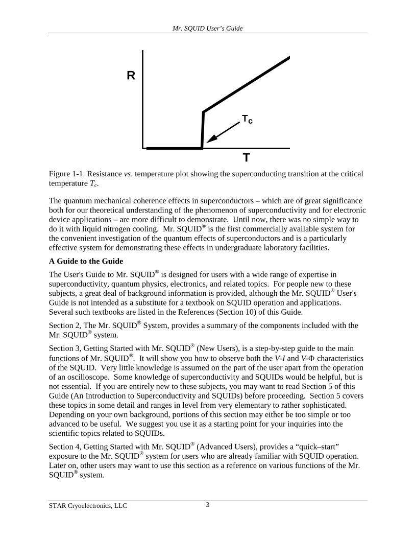
By attaching wires to a superconducting sample, one can just as easily demonstrate the zero resistance property of superconductors that gives them their name. A standard experiment is to monitor the electrical resistance of the sample as the temperature is lowered from room temperature. When the superconducting critical temperature (Tc) is reached, the resistance plummets abruptly to zero as the sample transitions to the superconducting state.
Mr. SQUID User’s Guide
STAR Cryoelectronics, LLC 3
R
T
Tc
Figure 1-1. Resistance vs. temperature plot showing the superconducting transition at the critical temperature Tc.
The quantum mechanical coherence effects in superconductors – which are of great significance both for our theoretical understanding of the phenomenon of superconductivity and for electronic device applications – are more difficult to demonstrate. Until now, there was no simple way to do it with liquid nitrogen cooling. Mr. SQUID® is the first commercially available system for the convenient investigation of the quantum effects of superconductors and is a particularly effective system for demonstrating these effects in undergraduate laboratory facilities.
A Guide to the Guide The User's Guide to Mr. SQUID® is designed for users with a wide range of expertise in superconductivity, quantum physics, electronics, and related topics. For people new to these subjects, a great deal of background information is provided, although the Mr. SQUID® User's Guide is not intended as a substitute for a textbook on SQUID operation and applications. Several such textbooks are listed in the References (Section 10) of this Guide.
Section 2, The Mr. SQUID® System, provides a summary of the components included with the Mr. SQUID® system.
Section 3, Getting Started with Mr. SQUID® (New Users), is a step-by-step guide to the main functions of Mr. SQUID®. It will show you how to observe both the V-I and V-Φ characteristics of the SQUID. Very little knowledge is assumed on the part of the user apart from the operation of an oscilloscope. Some knowledge of superconductivity and SQUIDs would be helpful, but is not essential. If you are entirely new to these subjects, you may want to read Section 5 of this Guide (An Introduction to Superconductivity and SQUIDs) before proceeding. Section 5 covers these topics in some detail and ranges in level from very elementary to rather sophisticated. Depending on your own background, portions of this section may either be too simple or too advanced to be useful. We suggest you use it as a starting point for your inquiries into the scientific topics related to SQUIDs.
Section 4, Getting Started with Mr. SQUID® (Advanced Users), provides a “quick–start” exposure to the Mr. SQUID® system for users who are already familiar with SQUID operation. Later on, other users may want to use this section as a reference on various functions of the Mr. SQUID® system.
Mr. SQUID User’s Guide
STAR Cryoelectronics, LLC 4
Section 5, An Introduction to Superconductivity and SQUIDs, contains background material describing the phenomenon of superconductivity with an emphasis on explaining how Mr. SQUID® works. In this section you will find discussions of superconducting rings, phase coherence, the Josephson effects, magnetic flux quantization, and basic SQUID operation, as well as a history of SQUIDs and a brief description of the methods used to make the SQUID in your Mr. SQUID® system.
Section 6, Troubleshooting and Getting Help, is provided to help you deal with some common problems encountered with SQUID operation. It also provides information on how to contact STAR Cryoelectronics with problems that you cannot solve yourself.
Section 7, Advanced Experiments, contains information on advanced experiments that are possible using Mr. SQUID® in conjunction with other instruments and materials, some background about STAR Cryoelectronics, the developer and manufacturer of Mr. SQUID®; technical specifications for Mr. SQUID®, and a reference section that lists some useful books on superconductivity and SQUID operation.
The Mr. SQUID® User's Guide is intended to be a complete reference for the Mr. SQUID® owner providing operating instructions, background information, and suggestions for additional experiments for the advanced user. We invite your contributions and comments to the Guide.
Mr. SQUID User’s Guide
STAR Cryoelectronics, LLC 5
2 THE MR. SQUID® SYSTEM
2.1 System Components The complete Mr. SQUID® system includes the following items:
• MS-EB03 electronic control box and external ±12 Volts DC power supply,
• Mr. SQUID probe with the SQUID sensor and mu-metal shield,
• Nine-pin DB-9 M/M cable to connect the probe to the electronics box, and
• 1 L liquid nitrogen dewar.
2.2 Additional Equipment Required In addition to the components included with the Mr. SQUID® system, there are a few additional items that the user must supply in order to operate the system:
• A two-channel oscilloscope capable of x-y display, or a PC-based digital oscilloscope (e.g., the Model DS1M12 “Stingray” USB digital oscilloscope available from EasySync Ltd.1
• BNC coaxial cables for connecting the electronics box to the output device. These are standard items for any laboratory using electronic instruments.
), or the optional USB Mr. SQUID Digitizer.
• Liquid nitrogen. The dewar included with Mr. SQUID® holds about 1 liter of liquid nitrogen, which should last for several hours. There are hazards associated with the use of liquid nitrogen and with vacuum vessels used to contain it – see instructions provided by the dewar manufacturer that are included with the dewar.
DIRECT SKIN EXPOSURE TO LIQUID NITROGEN CAN CAUSE SEVERE BURNS. Personnel experienced in the use of cryogenic liquids should be on hand for all experiments involving the use of liquid nitrogen and appropriate precautions must be taken. A special caution: when removing the Mr. SQUID® probe from the nitrogen dewar, be careful not to handle the cold end until it warms up completely (the frost and condensation will disappear when it has warmed completely).
1 www.usb-instruments.com..
Mr. SQUID User’s Guide
STAR Cryoelectronics, LLC 6
3 GETTING STARTED WITH MR. SQUID® (NEW USERS)
The directions that follow assume that you have some familiarity with the basics of superconductivity including zero resistance, flux quantization, and the Josephson effect. If not, you may wish to read some of Section 5, An Introduction to Superconductivity and SQUIDs, before going any further.
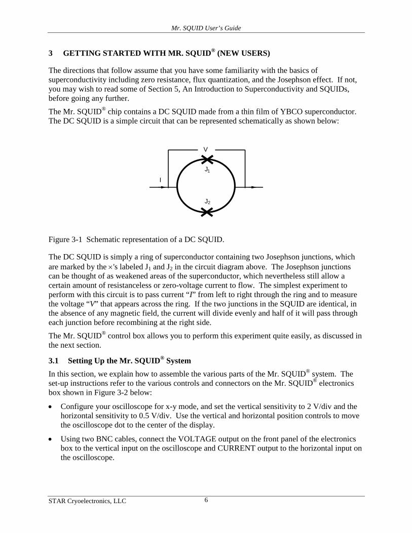
The Mr. SQUID® chip contains a DC SQUID made from a thin film of YBCO superconductor. The DC SQUID is a simple circuit that can be represented schematically as shown below:
V
J
J
1
2
I
Figure 3-1 Schematic representation of a DC SQUID.
The DC SQUID is simply a ring of superconductor containing two Josephson junctions, which are marked by the ×'s labeled J1 and J2 in the circuit diagram above. The Josephson junctions can be thought of as weakened areas of the superconductor, which nevertheless still allow a certain amount of resistanceless or zero-voltage current to flow. The simplest experiment to perform with this circuit is to pass current “I” from left to right through the ring and to measure the voltage “V” that appears across the ring. If the two junctions in the SQUID are identical, in the absence of any magnetic field, the current will divide evenly and half of it will pass through each junction before recombining at the right side.
The Mr. SQUID® control box allows you to perform this experiment quite easily, as discussed in the next section.
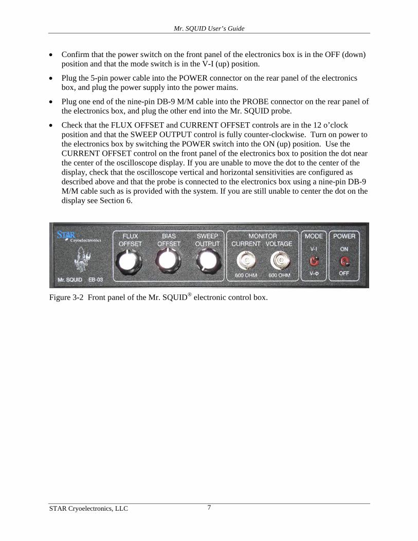
3.1 Setting Up the Mr. SQUID® System In this section, we explain how to assemble the various parts of the Mr. SQUID® system. The set-up instructions refer to the various controls and connectors on the Mr. SQUID® electronics box shown in Figure 3-2 below:
• Configure your oscilloscope for x-y mode, and set the vertical sensitivity to 2 V/div and the horizontal sensitivity to 0.5 V/div. Use the vertical and horizontal position controls to move the oscilloscope dot to the center of the display.
• Using two BNC cables, connect the VOLTAGE output on the front panel of the electronics box to the vertical input on the oscilloscope and CURRENT output to the horizontal input on the oscilloscope.
Mr. SQUID User’s Guide
STAR Cryoelectronics, LLC 7
• Confirm that the power switch on the front panel of the electronics box is in the OFF (down) position and that the mode switch is in the V-I (up) position.
• Plug the 5-pin power cable into the POWER connector on the rear panel of the electronics box, and plug the power supply into the power mains.
• Plug one end of the nine-pin DB-9 M/M cable into the PROBE connector on the rear panel of the electronics box, and plug the other end into the Mr. SQUID probe.
• Check that the FLUX OFFSET and CURRENT OFFSET controls are in the 12 o’clock position and that the SWEEP OUTPUT control is fully counter-clockwise. Turn on power to the electronics box by switching the POWER switch into the ON (up) position. Use the CURRENT OFFSET control on the front panel of the electronics box to position the dot near the center of the oscilloscope display. If you are unable to move the dot to the center of the display, check that the oscilloscope vertical and horizontal sensitivities are configured as described above and that the probe is connected to the electronics box using a nine-pin DB-9 M/M cable such as is provided with the system. If you are still unable to center the dot on the display see Section 6.
Figure 3-2 Front panel of the Mr. SQUID® electronic control box.

Mr. SQUID User’s Guide
STAR Cryoelectronics, LLC 8
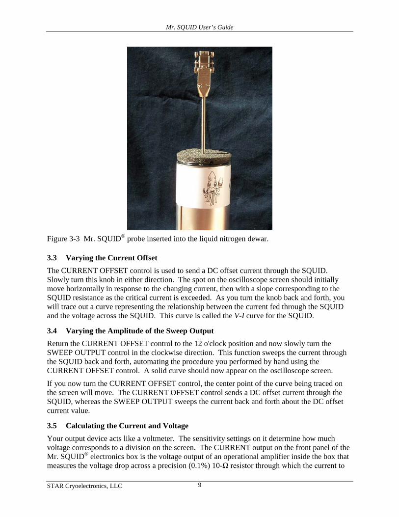
3.2 Cooling the Mr. SQUID® Probe
Fill the dewar about 3/4-full with liquid nitrogen. If you will be using the system for a long time (more than a few hours), the liquid nitrogen level in the dewar will decrease due to evaporation. If the liquid level drops below the SQUID sensor, simply refill the dewar to its original level with more liquid nitrogen.
Confirm that the mu-metal shield is securely installed on the Mr. SQUID probe. The mu-metal shield helps screen the SQUID from external magnetic noise sources.
Wear eye protection and gloves during the following procedure as the liquid nitrogen may splash as the probe is introduced into the dewar. Slowly lower the sensor end of the probe into the dewar taking care to avoid excess boiling and splashing of the liquid nitrogen. The foam cap for the Mr. SQUID® dewar has a hole and a slot in it to center the Mr. SQUID® probe in the dewar, as shown in Figure 3-3 below. It will take several minutes for the SQUID sensor at the end of the probe to reach the boiling point temperature of liquid nitrogen, 77 K (at sea level). The critical temperature (Tc) for the YBCO superconductor in Mr. SQUID® is approximately 90 K.
It is important to cool the SQUID into the superconducting state with a minimum of external magnetic fields present. This will reduce the effects of a phenomenon known as magnetic flux trapping, which will adversely affect the performance of the SQUID. We will discuss the consequences of flux-trapping later.
WARNING
WEAR EYE PROTECTION AND GLOVES WHEN WORKING WITH LIQUID NITROGEN. UNDER ALL CIRCUMSTANCES, BE SURE TO FOLLOW THE SAFETY REGULATIONS OF YOUR LABORATORY. IF YOU ARE UNCERTAIN ABOUT HANDLING LIQUID NITROGEN, CHECK WITH RESPONSIBLE PEOPLE IN YOUR LABORATORY. THE DEWAR SUPPLIED WITH MR. SQUID® IS MANUFACTURED SPECIFICALLY TO CONTAIN LIQUID NITROGEN, BUT IT CONSISTS OF A GLASS VACUUM VESSEL THAT CAN SHATTER IF MISHANDLED.
Mr. SQUID User’s Guide
STAR Cryoelectronics, LLC 9
Figure 3-3 Mr. SQUID® probe inserted into the liquid nitrogen dewar.
3.3 Varying the Current Offset The CURRENT OFFSET control is used to send a DC offset current through the SQUID. Slowly turn this knob in either direction. The spot on the oscilloscope screen should initially move horizontally in response to the changing current, then with a slope corresponding to the SQUID resistance as the critical current is exceeded. As you turn the knob back and forth, you will trace out a curve representing the relationship between the current fed through the SQUID and the voltage across the SQUID. This curve is called the V-I curve for the SQUID.
3.4 Varying the Amplitude of the Sweep Output Return the CURRENT OFFSET control to the 12 o'clock position and now slowly turn the SWEEP OUTPUT control in the clockwise direction. This function sweeps the current through the SQUID back and forth, automating the procedure you performed by hand using the CURRENT OFFSET control. A solid curve should now appear on the oscilloscope screen.
If you now turn the CURRENT OFFSET control, the center point of the curve being traced on the screen will move. The CURRENT OFFSET control sends a DC offset current through the SQUID, whereas the SWEEP OUTPUT sweeps the current back and forth about the DC offset current value.
3.5 Calculating the Current and Voltage Your output device acts like a voltmeter. The sensitivity settings on it determine how much voltage corresponds to a division on the screen. The CURRENT output on the front panel of the Mr. SQUID® electronics box is the voltage output of an operational amplifier inside the box that measures the voltage drop across a precision (0.1%) 10-Ω resistor through which the current to
Mr. SQUID User’s Guide
STAR Cryoelectronics, LLC 10
the SQUID flows. According to Ohm's Law (I = V/R), the current flowing through this resistor is equal to the voltage across it divided by the resistance. The operational amplifier is configured with a gain of 1,000 so a voltage of 1 V at the CURRENT monitor output corresponds to a current of (1/1,000)/10 = 1/10,000 A or 100 µA. Typical voltage levels across SQUIDs are very small and amplification is required to measure these voltages using an external display device such as an oscilloscope. The Mr. SQUID® electronic control box includes an amplifier circuit that can be configured for a gain of 100, 1,000 or 10,000 using an internal switch. For use with Mr. SQUID®, the default factory-configured gain setting is 10,000. Thus, to calculate the actual voltage across the SQUID, the measured value on the oscilloscope should be divided by 10,000. That is, 1 V at the VOLTAGE monitor output corresponds to 100 µV across the SQUID.
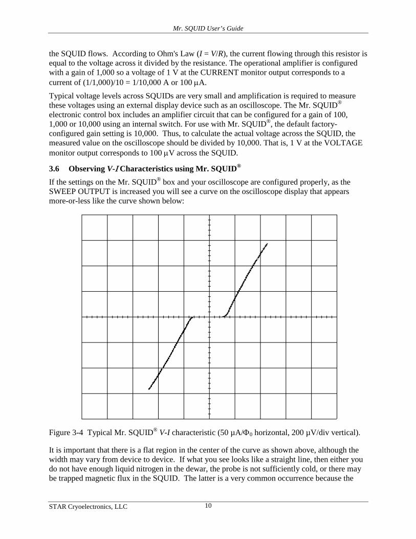
3.6 Observing V-Ι Characteristics using Mr. SQUID® If the settings on the Mr. SQUID® box and your oscilloscope are configured properly, as the SWEEP OUTPUT is increased you will see a curve on the oscilloscope display that appears more-or-less like the curve shown below:
Figure 3-4 Typical Mr. SQUID® V-I characteristic (50 µA/Φ0 horizontal, 200 µV/div vertical).
It is important that there is a flat region in the center of the curve as shown above, although the width may vary from device to device. If what you see looks like a straight line, then either you do not have enough liquid nitrogen in the dewar, the probe is not sufficiently cold, or there may be trapped magnetic flux in the SQUID. The latter is a very common occurrence because the
Mr. SQUID User’s Guide
STAR Cryoelectronics, LLC 11
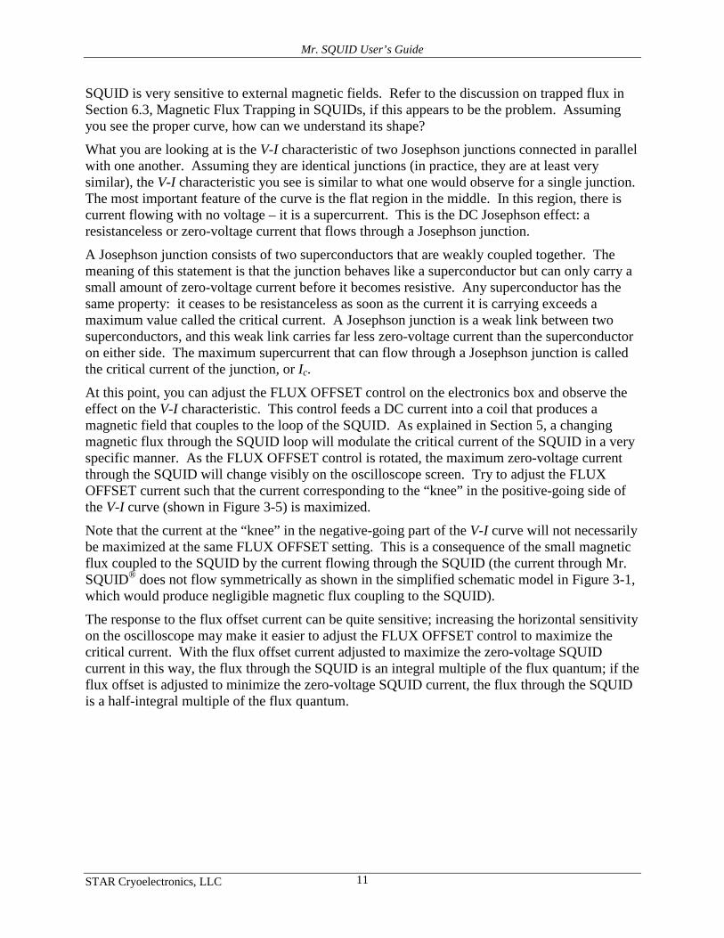
SQUID is very sensitive to external magnetic fields. Refer to the discussion on trapped flux in Section 6.3, Magnetic Flux Trapping in SQUIDs, if this appears to be the problem. Assuming you see the proper curve, how can we understand its shape?
What you are looking at is the V-I characteristic of two Josephson junctions connected in parallel with one another. Assuming they are identical junctions (in practice, they are at least very similar), the V-I characteristic you see is similar to what one would observe for a single junction. The most important feature of the curve is the flat region in the middle. In this region, there is current flowing with no voltage – it is a supercurrent. This is the DC Josephson effect: a resistanceless or zero-voltage current that flows through a Josephson junction.
A Josephson junction consists of two superconductors that are weakly coupled together. The meaning of this statement is that the junction behaves like a superconductor but can only carry a small amount of zero-voltage current before it becomes resistive. Any superconductor has the same property: it ceases to be resistanceless as soon as the current it is carrying exceeds a maximum value called the critical current. A Josephson junction is a weak link between two superconductors, and this weak link carries far less zero-voltage current than the superconductor on either side. The maximum supercurrent that can flow through a Josephson junction is called the critical current of the junction, or Ic.
At this point, you can adjust the FLUX OFFSET control on the electronics box and observe the effect on the V-I characteristic. This control feeds a DC current into a coil that produces a magnetic field that couples to the loop of the SQUID. As explained in Section 5, a changing magnetic flux through the SQUID loop will modulate the critical current of the SQUID in a very specific manner. As the FLUX OFFSET control is rotated, the maximum zero-voltage current through the SQUID will change visibly on the oscilloscope screen. Try to adjust the FLUX OFFSET current such that the current corresponding to the “knee” in the positive-going side of the V-I curve (shown in Figure 3-5) is maximized.
Note that the current at the “knee” in the negative-going part of the V-I curve will not necessarily be maximized at the same FLUX OFFSET setting. This is a consequence of the small magnetic flux coupled to the SQUID by the current flowing through the SQUID (the current through Mr. SQUID® does not flow symmetrically as shown in the simplified schematic model in Figure 3-1, which would produce negligible magnetic flux coupling to the SQUID).
The response to the flux offset current can be quite sensitive; increasing the horizontal sensitivity on the oscilloscope may make it easier to adjust the FLUX OFFSET control to maximize the critical current. With the flux offset current adjusted to maximize the zero-voltage SQUID current in this way, the flux through the SQUID is an integral multiple of the flux quantum; if the flux offset is adjusted to minimize the zero-voltage SQUID current, the flux through the SQUID is a half-integral multiple of the flux quantum.
Mr. SQUID User’s Guide
STAR Cryoelectronics, LLC 12
Figure 3-5. Location of “knee” in the SQUID V-I characteristic (100 µA/Φ0 horizontal, 200 µV/div vertical).
You can determine the critical current of the junctions in Mr. SQUID® by measuring the voltage at the “knee” in the V-I curve (after adjusting the FLUX OFFSET to maximize the zero-voltage current at the location of the “knee”) and dividing that number by 10,000 to convert your answer into Amperes of current. If the “knee” is at 0.5 Volt, for example, the corresponding current is 50 µA.
Since the V-I curve at the “knee” typically is rounded (owing to thermal noise), the critical current can more accurately be estimated as follows. Increase the horizontal and vertical sensitivities on the oscilloscope to magnify the region around the “knee”, and check that the horizontal and vertical inputs on the oscilloscope are zeroed at the center of the display. This can be done by grounding each input in turn and using the position controls on the oscilloscope to move the trace for the grounded input such that it coincides with the major axis through the center of the display.
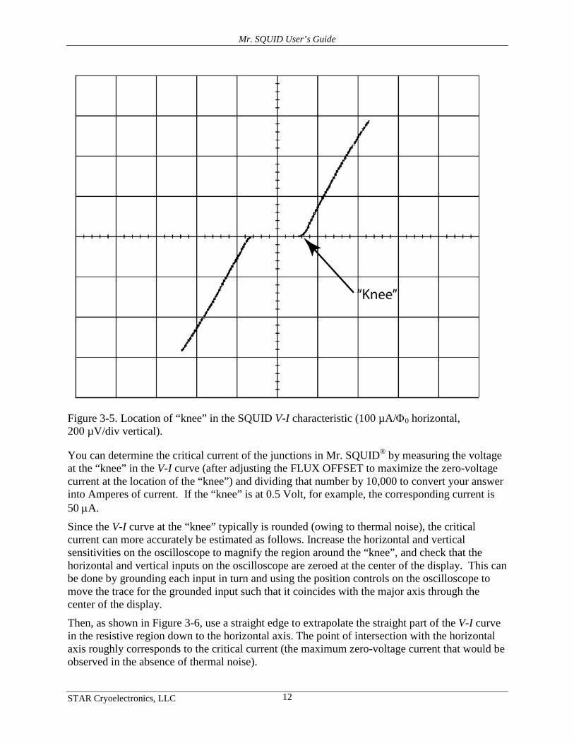
Then, as shown in Figure 3-6, use a straight edge to extrapolate the straight part of the V-I curve in the resistive region down to the horizontal axis. The point of intersection with the horizontal axis roughly corresponds to the critical current (the maximum zero-voltage current that would be observed in the absence of thermal noise).
Mr. SQUID User’s Guide
STAR Cryoelectronics, LLC 13
Figure 3-6. Method to determine the critical current 2Ic (20 µA/Φ0 horizontal, 10 µV/div vertical).
Note, however, that this is the current through both junctions in the SQUID, not just one. Therefore, assuming the junctions are identical, the current through one junction is half this value (in our example above, 50/2 = 25 µA).
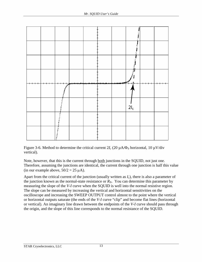
Apart from the critical current of the junction (usually written as Ic), there is also a parameter of the junction known as the normal-state resistance or RN. You can determine this parameter by measuring the slope of the V-I curve when the SQUID is well into the normal resistive region. The slope can be measured by increasing the vertical and horizontal sensitivities on the oscilloscope and increasing the SWEEP OUTPUT control almost to the point where the vertical or horizontal outputs saturate (the ends of the V-I curve “clip” and become flat lines (horizontal or vertical). An imaginary line drawn between the endpoints of the V-I curve should pass through the origin, and the slope of this line corresponds to the normal resistance of the SQUID.
Mr. SQUID User’s Guide
STAR Cryoelectronics, LLC 14
Figure 3-7 Determining the junction normal resistance RN from the SQUID V-I characteristic (50 µA/Φ0 horizontal, 200 µV/div vertical). The junction normal resistance is equal to twice the slope of the dashed line, or 2(∆V/∆I).
To measure the slope, ground the horizontal input on the oscilloscope and measure the voltage corresponding to the length of the vertical line displayed on the oscilloscope. This is the (amplified) voltage across the SQUID; to get the actual voltage you must divide this number by 10,000. Now reconfigure the horizontal input for DC coupling and ground the vertical input. Measure the voltage corresponding to the length of the horizontal line displayed on the oscilloscope. As described above, the actual current through the SQUID is equal to this voltage divided by 10,000. The normal resistance of the SQUID is then the voltage across the SQUID divided by the current through the SQUID.
Remember that the DC SQUID contains two junctions in parallel, so the resistance measured above corresponds to half the resistance of a single junction (assuming they are identical.) This means that the normal resistance RN of each Josephson junction is twice the normal resistance of the SQUID.
The product of the critical current and the normal state resistance (IcRN) is a voltage that is an important parameter for the SQUID. Make a note of it now for use later. Note that IcRN for one of the junctions has the same value for the SQUID, which has two junctions in parallel. For the
Mr. SQUID User’s Guide
STAR Cryoelectronics, LLC 15
junctions in Mr. SQUID® operating in liquid nitrogen, you will probably obtain a value between 100 and 200 µV. This value sets the maximum voltage change in the SQUID by an individual magnetic flux quantum, and is discussed later in this section.
3.7 Observing V-Φ Characteristics using Mr. SQUID® Up to this point, we have been looking at the properties of Josephson junctions. Now we will turn our attention to the properties of the DC SQUID itself. The DC SQUID has the remarkable property that there is a periodic relationship between the output voltage of the SQUID and applied magnetic flux. This relationship comes from the flux quantization property of superconducting rings that is discussed in detail in Section 5. The Mr. SQUID® electronics box will allow you to observe this periodic relationship in the form of V-Φ characteristics on your oscilloscope screen.
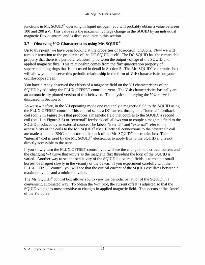
You have already observed the effects of a magnetic field on the V-I characteristics of the SQUID by adjusting the FLUX OFFSET control current. The V-Φ characteristics basically are an automatically plotted version of this behavior. The physics underlying the V-Φ curve is discussed in Section 5. As we saw before, in the V-I operating mode one can apply a magnetic field to the SQUID using the FLUX OFFSET control. This control sends a DC current through the “internal” feedback coil (coil 2 in Figure 3-8) that produces a magnetic field that couples to the SQUID; a second coil (coil 1 in Figure 3-8) or “external” feedback coil allows you to couple a magnetic field to the SQUID produced by an external source. The labels “internal” and “external” refer to the accessibility of the coils to the Mr. SQUID® user. Electrical connections to the “external” coil are made using the BNC connector on the back of the Mr. SQUID® electronics box. The “internal” coil is used by the Mr. SQUID® electronics to apply flux to the SQUID and is not directly accessible to the user.
If you slowly turn the FLUX OFFSET control, you will see the change in the critical current and the changing V-I curve that occurs as the magnetic flux threading the loop of the SQUID is varied. Another way to see the sensitivity of the SQUID to external fields is to rotate a small horseshoe magnet slowly in the vicinity of the dewar. If you experiment carefully with the FLUX OFFSET control, you will see that the critical current of the SQUID oscillates between a maximum value and a minimum value.
The Mr. SQUID® control box allows you to view the periodic behavior of the SQUID in a convenient, automated way. To obtain the V-Φ plot, the current offset is adjusted so that the SQUID voltage is most sensitive to changes in applied magnetic field. This occurs at the "knee" of the V-I curve.
Mr. SQUID User’s Guide
STAR Cryoelectronics, LLC 16
Figure 3-8 Photograph of the Mr. SQUID® chip showing the two feedback coils. Coil 1 is the “external” coil, coil 2 is the “internal” coil. See Sec. 9.2 for Mr. SQUID® specifications.
To find this point, first adjust the FLUX OFFSET control so that the zero-voltage current is at its largest value. Then, reduce the SWEEP OUTPUT control all the way so that only a point is visible on the oscilloscope screen. In this mode, you can then sweep the point along the V-I curve by adjusting the CURRENT OFFSET control such that the point rests at either knee in the V-I curve. Now turn the FLUX OFFSET control, which controls the amount of magnetic flux through the hole in the SQUID loop. You should see the point oscillate vertically on the screen as the FLUX OFFSET control is varied. This periodic motion arises because the screening current in the SQUID body depends on the applied magnetic flux in a periodic manner. The period is determined by the magnetic flux quantum (Φ0). This phenomenon is a manifestation of the macroscopic quantum nature of superconductivity.
To automate this procedure, configure the electronic control box for the V-Φ mode (MODE switch in the down position). In this mode, the sweep signal is sent through the feedback coil, which is linearly related to the magnetic field applied to the SQUID. Then, since the SQUID modulation signals are smaller than the junction voltages examined earlier, you will need to increase the sensitivity of the vertical input on the oscilloscope. The maximum peak-to-peak voltage swing of the SQUID modulation in Mr. SQUID® (∆V) typically is between 10 and 30 µV (or 100 to 300 mV at the front panel VOLTAGE output of the Mr. SQUID® electronics box). In this case, set the vertical sensitivity of your oscilloscope to 10 mV/div. In addition, if your oscilloscope can be operated in an AC-coupled mode on the vertical channel, use this mode for more convenient viewing of the V-Φ curve (never use the AC mode to look at the V-I curve, or it will be completely distorted on the oscilloscope screen.) In order to view several periods of oscillation, set the horizontal sensitivity to 50 mV/div.
Mr. SQUID User’s Guide
STAR Cryoelectronics, LLC 17
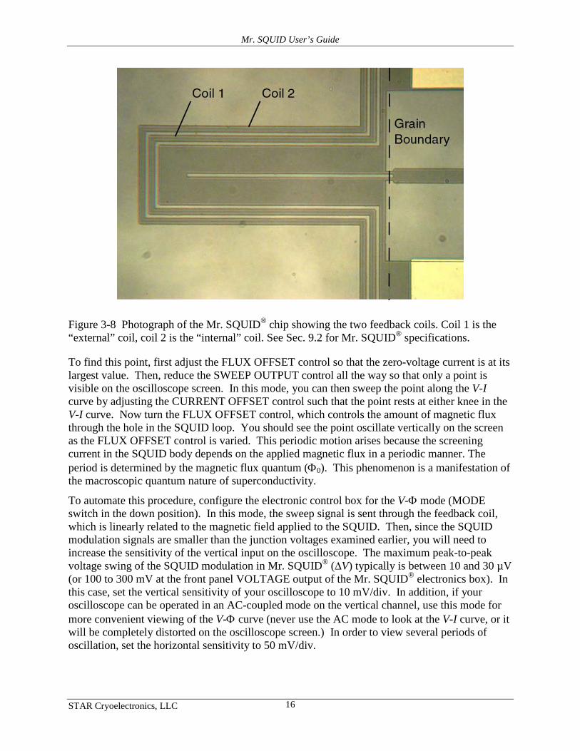
Now turn the SWEEP OUTPUT control in the clockwise direction. Depending on the particular SQUID and coil in your probe, you should be able to see at least four or five periods of oscillation as shown in Figure 3-9.
Figure 3-9 A typical Mr. SQUID® V-Φ characteristic (50 µA/Φ0 horizontal, 10 µV/div vertical). The maximum ∆V may range from 10 to 30 µV or higher.
The voltage change that occurs due to the influence of the magnetic field now appears on the vertical axis of your oscilloscope. You can maximize the signal by fine-tuning the CURRENT OFFSET control (just keep your eye on the V-Φ curve as you “tweak” the CURRENT OFFSET control until you get the maximum modulation or voltage swing ∆V). Since the voltage amplification provided by the Mr. SQUID® box is unchanged from before, to determine the actual voltage swing across the SQUID, you must divide the voltage swing displayed on the oscilloscope by 10,000.
Notice the effect that the FLUX OFFSET control has on the V-Φ curve. It allows you to set the central value of applied flux about which the SWEEP OUTPUT control varies the sweep signal. In other words, this control allows you to apply a static magnetic field to the SQUID on top of the oscillating field applied using the SWEEP OUTPUT control. Turning the FLUX OFFSET control will therefore allow you to move left and right along the V-Φ curve and thereby explore points along this curve. You can accomplish the same thing in a less controlled manner by waving a small permanent magnet near the probe. Another way to see the effect of an additional applied field is to carefully rotate the Mr. SQUID probe. This rotates the SQUID with respect to the Earth's magnetic field and causes a shift in the total magnetic field coupled to the SQUID.
Mr. SQUID User’s Guide
STAR Cryoelectronics, LLC 18
Actually, the magnetic shield on the probe screens out most of the Earth’s field, but the amount of field that gets by the shield is quite enough to move the V-Φ pattern noticeably on the screen.
Later on, you may want to warm the probe to room temperature and remove the magnetic shield from the bottom of the probe. This may be done by removing the small setscrew that supports the shield. Set both the shield and the screw aside in a safe place so that they can be reinstalled later. If you now cool the probe and set up the V-Φ measurement, you will find that the SQUID is tremendously more sensitive to the local environment. In fact, you may have a great deal of difficulty in getting a good V-I curve without flux trapping (see the discussion in Section 6). Assuming you succeed in observing the V-Φ curve without the magnetic shield (which may be impossible in many environments), you will find that almost any magnetic disturbance anywhere near the dewar will be visible on the oscilloscope display. Try swiveling a metal chair, for example!
The most sensitive mode of operating a SQUID is to “flux-lock” the SQUID using closed loop feedback electronics. In the flux-locked loop (FFL) mode, a feedback current is used to counteract any change in external magnetic field. By measuring the amount of feedback current needed to exactly counteract the external magnetic field, it is possible to detect magnetic fields corresponding to a tiny fraction of the characteristic field required to produce a quantum of flux through the SQUID. This experiment is detailed in Section 7, Advanced Experiments.
3.8 Additional SQUID Measurements Now that you can measure a variety of properties of the SQUID in the Mr. SQUID® probe, you can determine a key parameter of the device, namely the ßL parameter. This is defined by
Eqn. 3-1 0
2Φ
=βLIc
L
where L is the inductance of the SQUID loop.
Earlier we mentioned that the maximum modulation voltage depth ∆V as measured from the V-Φ curve is related to the IcRN product that can be determined from the V-I curve. As we will discuss in Section 5, this relationship can be expressed simply in terms of the ßL parameter.
Eqn. 3-2 14
−∆π
=βVRI Nc
L
The above expression provides an approximate way to determine the ßL parameter empirically (i.e., without knowing the inductance L of the SQUID). This expression is strictly correct only if the critical currents of the two junctions are equal and only if thermal noise effects are negligible. Both of these are approximations for the junctions in your Mr. SQUID®.
The inductance of the Mr. SQUID® chip (see Figure 3-8) may be written as the sum of three terms,
Eqn. 3-3 jksl LLLL ++= ,
Mr. SQUID User’s Guide
STAR Cryoelectronics, LLC 19
where Lsl is the inductance of the long slit in the SQUID body, Lk is the small kinetic inductance of the SQUID body (arising from the “inertia” of the electrons2
The horizontal axis of the V-Φ curve measures the current through the feedback coil, and this is linearly related to the magnetic flux in the SQUID. The current gain in the Mr. SQUID® electronics box is 10,000 V/A (i.e., 1 Volt = 10-4 Amperes). The period of the modulation of the magnetic flux in the Mr. SQUID® loop is the flux quantum, Φ0 (2.07×10⁻¹⁵ Wb in MKS units.) By measuring the amount of current (∆I) in the coil that is required to produce a change of one fluxon through the SQUID, you can determine the mutual inductance (M) of the internal feedback coil with respect to the SQUID, using the following formula:
), and Lj is the inductance of the Josephson junction bridges, which also includes a small kinetic inductance contribution. The slit inductance per unit length is about 0.46 pH/µm, and the slit length (excluding the length of the junction bridges) is 125 µm. Then, Lsl = 58 pH. The kinetic inductance of the SQUID body is more difficult to determine precisely but is estimated to be about 7 pH. The inductance of the Josephson junction bridges is estimated to be about 8 pH, which includes the kinetic inductance contribution (the inductance per unit length of the bridges is much higher than 0.46 pH/µm because of the narrow width of the bridges). Thus, the total inductance is approximately L = 73 pH.
Eqn. 3-4 I
M∆Φ
= 0
You can find the value of ßL for the SQUID in your Mr. SQUID® probe using Eqn. 3-1, your measurement of Ic, and L ≈ 73 pH. From the measured values of Ic and ∆V, you can calculate ßL using Eqn. 3-2. Compare these two values. Do they agree?
The fact that the values calculated using Eqn. 3-1 and Eqn. 3-2 do not agree was a mystery for a number of years after the 1986 discovery of high-Tc superconductors, as these equations worked quite well for SQUIDs made using traditional low-Tc superconductors. This lack of agreement was resolved in 1993 with the recognition that thermal effects play a large role in the behavior of high-Tc SQUIDs. 3 Eqn. 3-1 The lack of agreement between and Eqn. 3-2 is in large part due to the fact that the Mr. SQUID® is at a relatively high temperature where thermal energies (kBT) are no longer small compared to the energy of a flux quantum ( L2
0Φ ). The relationship between the observed voltage modulation and ßL at a nonzero temperature T changes Eqn. 3-2 to:3
Eqn. 3-5 157.314
0
−
Φ−
∆π=β
TLkVRI BNc
L
Figure 3-10 illustrates the differences between the ßL values calculated using Eqn. 3-1, Eqn. 3-2, and Eqn. 3-5.
2 Principles of Superconductive Devices and Circuits, T. Van Duzer and C.W. Turner (Elsevier, New York, 1981) pp 114-116. 3 K. Enpuku, Y. Shimomura, and T. Kisu, “Effect of thermal noise on the characteristics of a high Tc superconducting quantum interference device”, J. Appl. Phys. 73, 7929 (1993)
Mr. SQUID User’s Guide
STAR Cryoelectronics, LLC 20
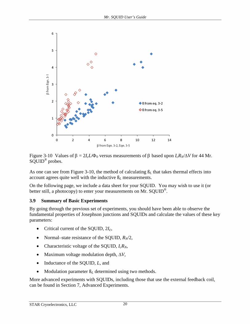
Figure 3-10 Values of β = 2IcL/Φ0 versus measurements of β based upon IcRN/∆V for 44 Mr. SQUID® probes.
As one can see from Figure 3-10, the method of calculating ßL that takes thermal effects into account agrees quite well with the inductive ßL measurements.
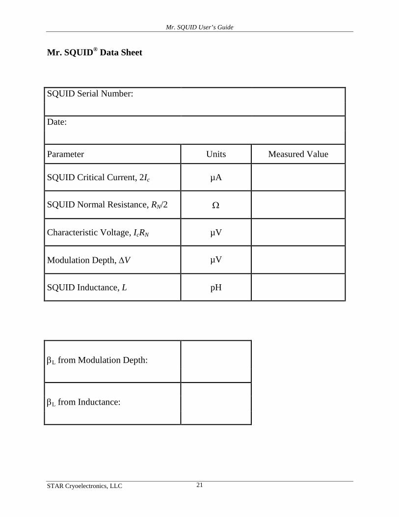
On the following page, we include a data sheet for your SQUID. You may wish to use it (or better still, a photocopy) to enter your measurements on Mr. SQUID®.
3.9 Summary of Basic Experiments By going through the previous set of experiments, you should have been able to observe the fundamental properties of Josephson junctions and SQUIDs and calculate the values of these key parameters:
• Critical current of the SQUID, 2Ic,
• Normal–state resistance of the SQUID, RN/2,
• Characteristic voltage of the SQUID, IcRN,
• Maximum voltage modulation depth, ∆V,
• Inductance of the SQUID, L, and
• Modulation parameter ßL determined using two methods. More advanced experiments with SQUIDs, including those that use the external feedback coil, can be found in Section 7, Advanced Experiments.
Mr. SQUID User’s Guide
STAR Cryoelectronics, LLC 21
Mr. SQUID® Data Sheet
SQUID Serial Number:
Date:
Parameter Units Measured Value
SQUID Critical Current, 2Ic µA
SQUID Normal Resistance, RN/2 Ω
Characteristic Voltage, IcRN µV
Modulation Depth, ∆V µV
SQUID Inductance, L pH
βL from Modulation Depth:
βL from Inductance:
Mr. SQUID User’s Guide
STAR Cryoelectronics, LLC 22
4 GETTING STARTED WITH MR. SQUID® (ADVANCED USERS)
This section is meant to give a quick explanation of the procedures for operating Mr. SQUID® and the features of the Mr. SQUID® control box, and assumes a previous knowledge of superconductivity and SQUIDs. The same information is provided in far greater detail in Section 3.
The Mr. SQUID® probe contains a DC SQUID fabricated from a thin-film of YBCO superconductor. The Josephson junctions are made using a junction process described at the end of Section 5. Flux is coupled to the SQUID via two separate 3/4-turn coils closely spaced around the outside of the SQUID (see Figure 3-8). Input to the feedback coil is made directly through the main cable in the system; the flux offset current is supplied by the Mr. SQUID® electronics box. Input to the external coil is at the discretion of the user. Terminals are available both at room temperature (through a BNC connector on the back of the electronics box for voltage input signals) and at low temperature through terminals at the bottom of the probe (for current input signals). The probe is equipped with a removable mu-metal magnetic shield to attenuate external magnetic fields. The SQUID chip itself is encased in an epoxy capsule that protects it from water vapor and ensures that it is cooled and warmed relatively slowly.
The Mr. SQUID® electronics box is designed to provide all the electronics necessary to observe the basic functions of a DC SQUID. Included is a low-noise amplifier section that amplifies the output voltage of the SQUID (with switch-configurable gains of 100, 1,000 and 10,000; the latter is the factory-configured default setting for Mr. SQUID®), current driver circuits to bias the SQUID and drive the feedback coil, and the switching required for the various functions. An internal triangle wave test signal is used to display the SQUID V-I and V-Φ characteristics on an oscilloscope. The default frequency is 20 Hz but may be adjusted over a frequency range from 10 to 50 Hz.
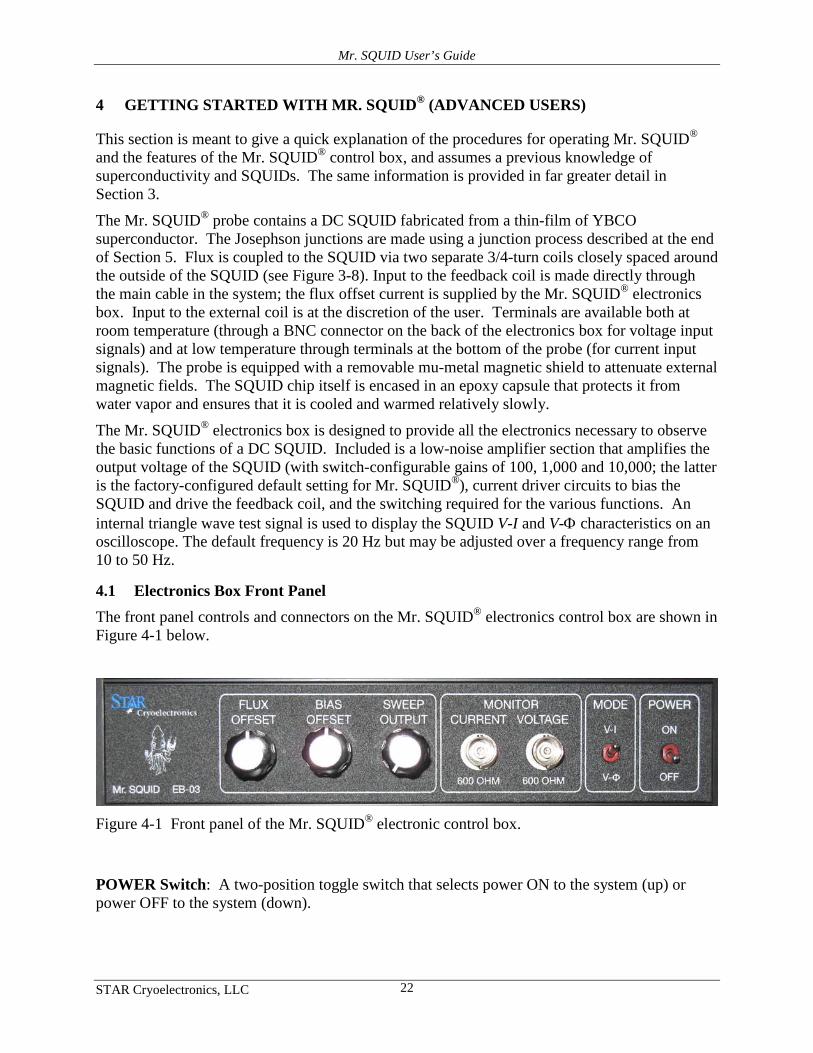
4.1 Electronics Box Front Panel The front panel controls and connectors on the Mr. SQUID® electronics control box are shown in Figure 4-1 below.
Figure 4-1 Front panel of the Mr. SQUID® electronic control box.
POWER Switch: A two-position toggle switch that selects power ON to the system (up) or power OFF to the system (down).
Mr. SQUID User’s Guide
STAR Cryoelectronics, LLC 23
MODE Switch: A two-position toggle switch that selects between the V–I (up) and V–Φ (down) modes.
• In V–I mode, the triangle wave test signal is applied across the SQUID bias terminals.
• In V–Φ mode, the triangle wave test signal is applied to a feedback coil that is inductively coupled to the SQUID.
VOLTAGE Output: A BNC connector providing the amplified voltage across the SQUID. The Mr. SQUID® electronics box includes an amplifier circuit that can be configured for a gain of 100, 1,000 or 10,000 using an internal switch. For use with Mr. SQUID®, the default factory-configured gain setting is 10,000. Thus, the actual voltage across the SQUID is the voltage at the VOLTAGE output divided by 10,000. (i.e., 1 V at the VOLTAGE output corresponds to 100 µV across the SQUID).
CURRENT Output: A BNC connector providing a voltage signal proportional to the current output of the Mr. SQUID® box. The CURRENT output signal is the voltage output of an operational amplifier inside the Mr. SQUID electronics box that measures the voltage drop across a precision (0.1%) 10 Ω resistor through which the current flows. According to Ohm's Law (I = V/R), the current flowing through this resistor is equal to the voltage across it divided by the resistance, 10.0 Ω. The operational amplifier is configured with a gain of 1,000 so a voltage of 1 V at the CURRENT monitor output corresponds to a current of (1/1,000)/10 = 1/10,000 A or 100 µA.
• In the V–I mode, the CURRENT output represents the current through the SQUID (the sum of the triangle wave plus the DC bias offset current set by the CURRENT OFFSET control).
• In the V–Φ mode, the CURRENT output represents the current through the feedback coil (the sum of the triangle wave plus the DC flux offset current set by the Flux Bias control).
SWEEP OUTPUT control: Sets the amplitude of the triangle wave test signal in either the V–I or V–Φ mode.
In either mode, use the SWEEP OUTPUT control to set the width of the test signal sweep. In V-I mode, the triangle wave is applied to the bias (I) terminals of the SQUID; in V-Φ mode, the triangle wave is applied to the “internal” feedback coil.
CURRENT OFFSET control: Applies a positive or negative DC bias current to the SQUID. In the 12 o'clock position, this current is approximately zero.
This control is used to apply a DC bias offset current to the SQUID.
FLUX OFFSET control: Applies a positive or negative DC current to the “internal” feedback coil, which produces a DC magnetic field that is coupled to the SQUID. In the 12 o'clock position, this current is approximately zero.
This control is used to modulate the critical current of the SQUID manually by the application of an external magnetic flux produced by the current in the feedback coil.
Mr. SQUID User’s Guide
STAR Cryoelectronics, LLC 24
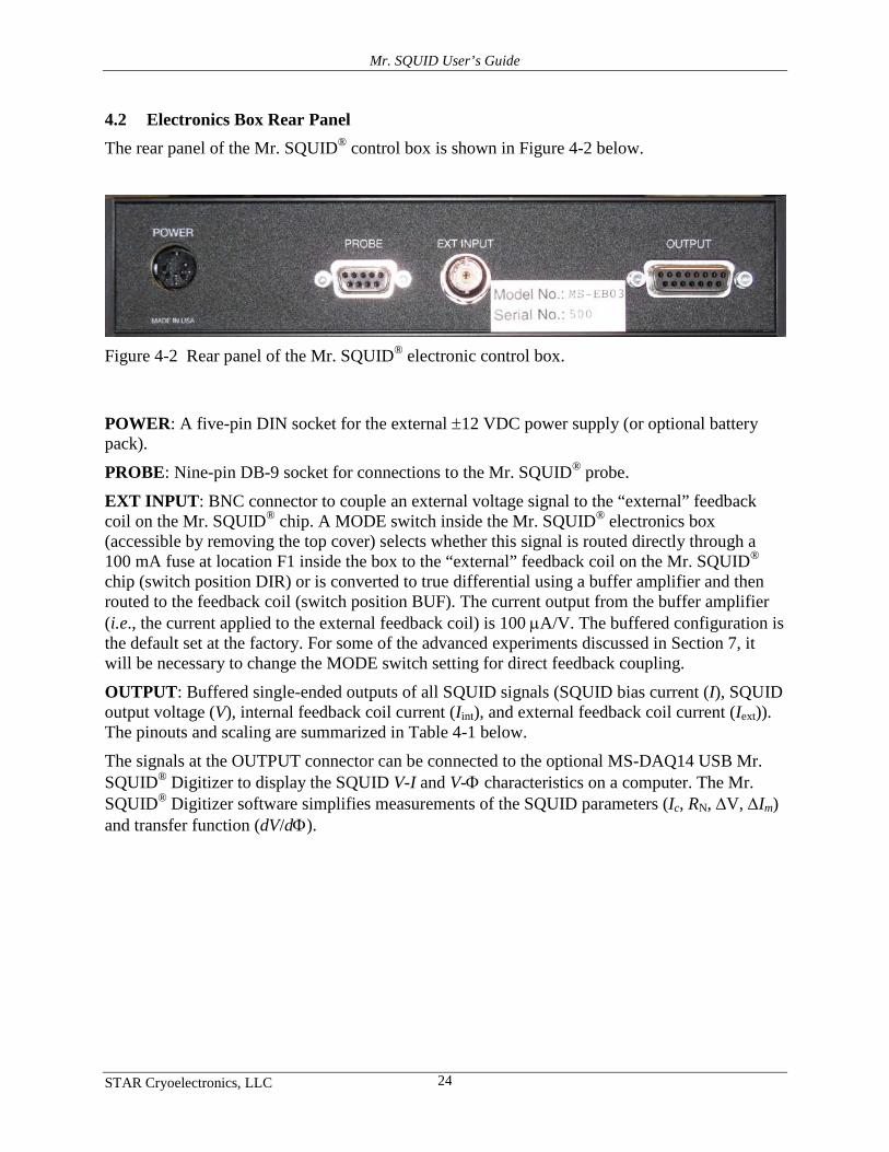
4.2 Electronics Box Rear Panel The rear panel of the Mr. SQUID® control box is shown in Figure 4-2 below.
Figure 4-2 Rear panel of the Mr. SQUID® electronic control box.
POWER: A five-pin DIN socket for the external ±12 VDC power supply (or optional battery pack).
PROBE: Nine-pin DB-9 socket for connections to the Mr. SQUID® probe.
EXT INPUT: BNC connector to couple an external voltage signal to the “external” feedback coil on the Mr. SQUID® chip. A MODE switch inside the Mr. SQUID® electronics box (accessible by removing the top cover) selects whether this signal is routed directly through a 100 mA fuse at location F1 inside the box to the “external” feedback coil on the Mr. SQUID® chip (switch position DIR) or is converted to true differential using a buffer amplifier and then routed to the feedback coil (switch position BUF). The current output from the buffer amplifier (i.e., the current applied to the external feedback coil) is 100 µA/V. The buffered configuration is the default set at the factory. For some of the advanced experiments discussed in Section 7, it will be necessary to change the MODE switch setting for direct feedback coupling.
OUTPUT: Buffered single-ended outputs of all SQUID signals (SQUID bias current (I), SQUID output voltage (V), internal feedback coil current (Iint), and external feedback coil current (Iext)). The pinouts and scaling are summarized in Table 4-1 below.
The signals at the OUTPUT connector can be connected to the optional MS-DAQ14 USB Mr. SQUID® Digitizer to display the SQUID V-I and V-Φ characteristics on a computer. The Mr. SQUID® Digitizer software simplifies measurements of the SQUID parameters (Ic, RN, ∆V, ∆Im) and transfer function (dV/dΦ).
Mr. SQUID User’s Guide
STAR Cryoelectronics, LLC 25
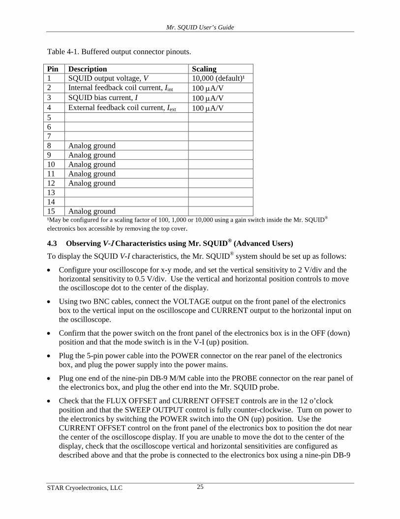
Table 4-1. Buffered output connector pinouts.
Pin Description Scaling 1 SQUID output voltage, V 10,000 (default)¹ 2 Internal feedback coil current, Iint 100 µA/V 3 SQUID bias current, I 100 µA/V 4 External feedback coil current, Iext 100 µA/V 5 6 7 8 Analog ground 9 Analog ground 10 Analog ground 11 Analog ground 12 Analog ground 13 14 15 Analog ground ¹May be configured for a scaling factor of 100, 1,000 or 10,000 using a gain switch inside the Mr. SQUID® electronics box accessible by removing the top cover.
4.3 Observing V-Ι Characteristics using Mr. SQUID® (Advanced Users) To display the SQUID V-I characteristics, the Mr. SQUID® system should be set up as follows:
• Configure your oscilloscope for x-y mode, and set the vertical sensitivity to 2 V/div and the horizontal sensitivity to 0.5 V/div. Use the vertical and horizontal position controls to move the oscilloscope dot to the center of the display.
• Using two BNC cables, connect the VOLTAGE output on the front panel of the electronics box to the vertical input on the oscilloscope and CURRENT output to the horizontal input on the oscilloscope.
• Confirm that the power switch on the front panel of the electronics box is in the OFF (down) position and that the mode switch is in the V-I (up) position.
• Plug the 5-pin power cable into the POWER connector on the rear panel of the electronics box, and plug the power supply into the power mains.
• Plug one end of the nine-pin DB-9 M/M cable into the PROBE connector on the rear panel of the electronics box, and plug the other end into the Mr. SQUID probe.
• Check that the FLUX OFFSET and CURRENT OFFSET controls are in the 12 o’clock position and that the SWEEP OUTPUT control is fully counter-clockwise. Turn on power to the electronics by switching the POWER switch into the ON (up) position. Use the CURRENT OFFSET control on the front panel of the electronics box to position the dot near the center of the oscilloscope display. If you are unable to move the dot to the center of the display, check that the oscilloscope vertical and horizontal sensitivities are configured as described above and that the probe is connected to the electronics box using a nine-pin DB-9
Mr. SQUID User’s Guide
STAR Cryoelectronics, LLC 26
M/M cable such as is provided with the system. If you are still unable to center the dot on the display see Section 6.
Fill the dewar about 3/4-full with liquid nitrogen. If you will be using the system for a long time (more than a few hours), the liquid nitrogen level in the dewar will decrease due to evaporation. If the liquid level dips below that of the SQUID sensor, simply refill the dewar to its original level with more liquid nitrogen.
Confirm that the mu-metal shield is securely installed on the Mr. SQUID probe. The mu-metal shield helps screen the SQUID from external magnetic noise sources.
Wear eye protection and gloves during the following procedure as the liquid nitrogen may splash as the probe is introduced into the dewar. Slowly lower the sensor end of the probe into the dewar taking care to avoid excess boiling and splashing of the liquid nitrogen. The foam cap for the Mr. SQUID® dewar has a hole and a slot in it to center the Mr. SQUID® probe in the dewar, as shown in Figure 3-3 below. It will take several minutes for the SQUID sensor at the end of the probe to reach the boiling point temperature of liquid nitrogen, 77 K (at sea level). The critical temperature (Tc) for the YBCO superconductor in Mr. SQUID® is approximately 90 K.
It is important to cool the SQUID into the superconducting state with a minimum of external magnetic fields present. This will reduce the effects of a phenomenon known as magnetic flux trapping, which will adversely affect the performance of the SQUID. We will discuss the consequences of flux-trapping later.
Zero the and CURRENT OFFSET controls (set them at 12 o'clock) and increase the SWEEP OUTPUT. The V-I curve should appear on your oscilloscope display. The CURRENT OFFSET control can be used to symmetrize the trace, if necessary, and the FLUX OFFSET control can be adjusted to maximize the critical current. A typical Mr. SQUID® V-I curve is shown in Figure 4-3 below.
WARNING
WEAR EYE PROTECTION AND GLOVES WHEN WORKING WITH LIQUID NITROGEN. UNDER ALL CIRCUMSTANCES, BE SURE TO FOLLOW THE SAFETY REGULATIONS OF YOUR LABORATORY. IF YOU ARE UNCERTAIN ABOUT HANDLING LIQUID NITROGEN, CHECK WITH RESPONSIBLE PEOPLE IN YOUR LABORATORY. THE DEWAR SUPPLIED WITH MR. SQUID® IS MANUFACTURED SPECIFICALLY TO CONTAIN LIQUID NITROGEN, BUT IT CONSISTS OF A GLASS VACUUM VESSEL THAT CAN SHATTER IF MISHANDLED.
Mr. SQUID User’s Guide
STAR Cryoelectronics, LLC 27
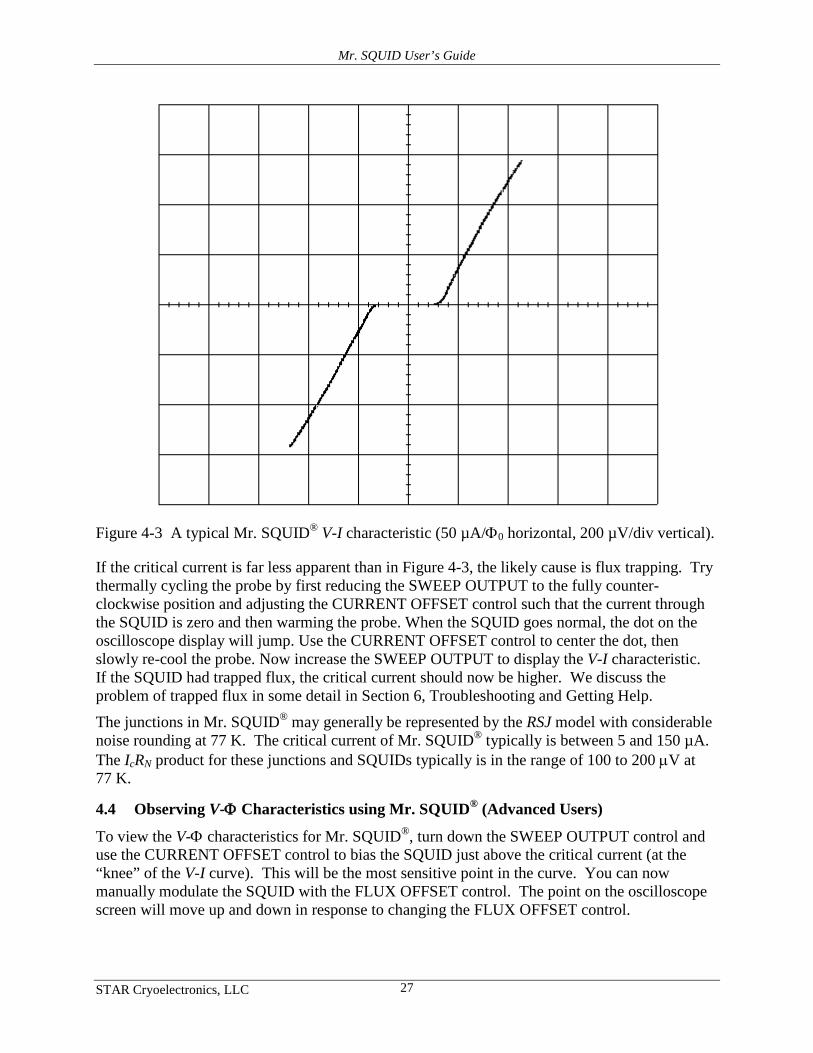
Figure 4-3 A typical Mr. SQUID® V-I characteristic (50 µA/Φ0 horizontal, 200 µV/div vertical).
If the critical current is far less apparent than in Figure 4-3, the likely cause is flux trapping. Try thermally cycling the probe by first reducing the SWEEP OUTPUT to the fully counter-clockwise position and adjusting the CURRENT OFFSET control such that the current through the SQUID is zero and then warming the probe. When the SQUID goes normal, the dot on the oscilloscope display will jump. Use the CURRENT OFFSET control to center the dot, then slowly re-cool the probe. Now increase the SWEEP OUTPUT to display the V-I characteristic. If the SQUID had trapped flux, the critical current should now be higher. We discuss the problem of trapped flux in some detail in Section 6, Troubleshooting and Getting Help.
The junctions in Mr. SQUID® may generally be represented by the RSJ model with considerable noise rounding at 77 K. The critical current of Mr. SQUID® typically is between 5 and 150 µA. The IcRN product for these junctions and SQUIDs typically is in the range of 100 to 200 µV at 77 K.
4.4 Observing V-Φ Characteristics using Mr. SQUID® (Advanced Users)
To view the V-Φ characteristics for Mr. SQUID®, turn down the SWEEP OUTPUT control and use the CURRENT OFFSET control to bias the SQUID just above the critical current (at the “knee” of the V-I curve). This will be the most sensitive point in the curve. You can now manually modulate the SQUID with the FLUX OFFSET control. The point on the oscilloscope screen will move up and down in response to changing the FLUX OFFSET control.
Mr. SQUID User’s Guide
STAR Cryoelectronics, LLC 28
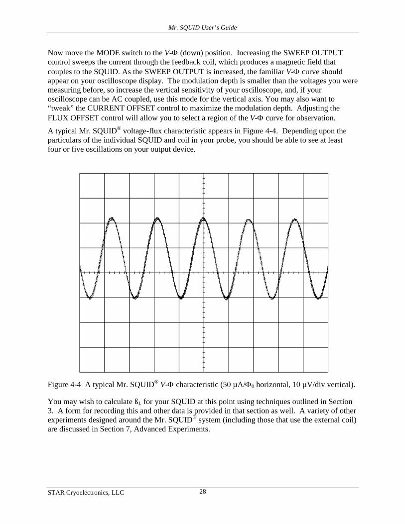
Now move the MODE switch to the V-Φ (down) position. Increasing the SWEEP OUTPUT control sweeps the current through the feedback coil, which produces a magnetic field that couples to the SQUID. As the SWEEP OUTPUT is increased, the familiar V-Φ curve should appear on your oscilloscope display. The modulation depth is smaller than the voltages you were measuring before, so increase the vertical sensitivity of your oscilloscope, and, if your oscilloscope can be AC coupled, use this mode for the vertical axis. You may also want to “tweak” the CURRENT OFFSET control to maximize the modulation depth. Adjusting the FLUX OFFSET control will allow you to select a region of the V-Φ curve for observation. A typical Mr. SQUID® voltage-flux characteristic appears in Figure 4-4. Depending upon the particulars of the individual SQUID and coil in your probe, you should be able to see at least four or five oscillations on your output device.
Figure 4-4 A typical Mr. SQUID® V-Φ characteristic (50 µA/Φ0 horizontal, 10 µV/div vertical).
You may wish to calculate ßL for your SQUID at this point using techniques outlined in Section 3. A form for recording this and other data is provided in that section as well. A variety of other experiments designed around the Mr. SQUID® system (including those that use the external coil) are discussed in Section 7, Advanced Experiments.
Mr. SQUID User’s Guide
STAR Cryoelectronics, LLC 29
5 AN INTRODUCTION TO SUPERCONDUCTIVITY AND SQUIDS
5.1 A Capsule History of Superconductivity Superconductivity was first discovered in 1911 in a sample of mercury metal that lost its resistance just four degrees above absolute zero. The phenomenon of superconductivity has been the subject of both scientific research and application development ever since. The ability to perform experiments at temperatures close to absolute zero was rare in the first half of this century and superconductivity research proceeded in relatively few laboratories. The first experiments only revealed the zero resistance property of superconductors, and more than twenty years passed before the ability of superconductors to expel magnetic flux (the Meissner Effect) was first observed. Magnetic flux quantization – the key to SQUID operation – was predicted theoretically only in 1950 and was finally observed in 1961. The Josephson effects were predicted and experimentally verified a few years after that.
SQUIDs were first studied in the mid-1960’s, soon after the first Josephson junctions were made. Practical superconducting wire for use in moving machines and magnets also became available in the 1960's. For the next twenty years, the field of superconductivity slowly progressed toward practical applications and to a more profound understanding of the underlying phenomena. A great revolution in superconductivity came in 1986 when the era of high-temperature superconductivity began. The existence of superconductivity at liquid nitrogen temperatures has opened the door to applications that are simpler and more convenient than were ever possible before. Nevertheless, the product you have in your hands today was made possible by many aspects of the 80 years of discovery that preceded it.
5.2 Superconductivity: A Quantum Mechanical Phenomenon There are certain materials – actually, many thousands of them by now – that exhibit a remarkable transition in their ability to pass electrical currents: when they are cooled down to a sufficiently low temperature, their electrical resistance vanishes completely. How this behavior comes about was a mystery that occupied the minds of theoretical physicists for nearly half a century after it was first observed. The answer turned out to be tied to the quantum-mechanical nature of solids, in particular, to the tendency of electrons to become paired. These “Cooper pairs” behave cooperatively in certain materials and form a single quantum-mechanical state.
In the following discussions, we can only explain these concepts briefly and without theoretical rigor. This User's Guide is not intended to be a textbook on quantum mechanics or on superconductivity. Fortunately, many such books exist and we refer you to some in the References in Section 10. What this Guide will try to do is give you some idea of the underlying physical principles behind Mr. SQUID®.
5.3 The Superconducting State A fundamental aspect of physical systems is that they naturally seek a state of lowest energy. An example of this is that a ball will roll to the lowest spot on an uneven surface (the lowest potential energy). An external source of energy (such as kicking the ball) is required to raise it to a higher spot (energy level). Similarly, systems of particles, such as the electrons in a metal, will occupy the lowest-energy state known as the ground state, unless they are excited by some external source of energy. In certain materials, it is possible for electrons to achieve a ground
Mr. SQUID User’s Guide
STAR Cryoelectronics, LLC 30
state with lower energy than otherwise available by entering the superconducting state. What is this state?
The Nobel Prize in Physics was awarded for the development of the theory that describes this state. Simply put, the superconducting ground state is one in which electrons pair up with one another such that each resultant pair has the same net momentum (which is zero if no current is flowing). In this ground state, all the electrons are described by the same wavefunction. What does this mean?
In quantum mechanics (also called “wave mechanics”), physical entities such as electrons are described mathematically by wavefunctions. Like ordinary waves in water or electromagnetic waves such as light waves, quantum mechanical wavefunctions are described by an amplitude (the height of the wave) and a phase (whether it is at a crest or a trough or somewhere in between). When you are describing waves of any kind, these two parameters are all that is necessary to specify what part of the wave you are discussing and how large it is. Moving waves oscillate both in time and in space. If we sit at one point in space, the wavefront will move up and down in time. If we look at one moment in time, the wavefront undulates in space. The quantum mechanical wavefunction is a mathematical entity that describes the behavior of physical systems such as electrons and light waves. A unique property of quantum mechanics is the interchangeability of particles and waves in describing physical systems.
Generally, there will be a unique wavefunction required to describe each particle in a physical system. In the usual or “normal” state, the wavefunctions describing the electrons in a material are unrelated to one another. In a superconductor, on the other hand, a single wavefunction describes the entire population of superconducting electron pairs. That wave function may differ in phase from one place to another within the superconductor, but knowing the function in one place determines it in another. Physicists call such a wavefunction a “many-body wavefunction.” Strictly speaking, electrons are indistinguishable particles; there is no way to keep track of an individual electron in the population and it in fact has no meaning to speak of one. The pairs of electrons that comprise the superconducting state are constantly forming, breaking, and reforming such that the wavefunction that describes the superconducting state remains the same. As we will see, it is the existence of this coherent wavefunction that accounts for the phenomena associated with superconductivity.
5.4 The Quantum of Flux Quantum mechanics is the modern theory of physical world in which matter and energy at their most fundamental levels occur in discrete chunks called quanta rather than being continuously divisible. We are familiar with this concept with respect to electrical charge, for example. To our knowledge, all electrical charge (excluding quarks for the moment) occurs in units of 1.6×10⁻¹⁹ coulombs, the charge on a single electron. Therefore, nothing in nature has 1.5 times this charge, for example. Electromagnetic energy is quantized in units called photons, whose magnitude is set by the product of the frequency of the radiation times a fundamental constant called Planck's constant (written simply as “h”). In general, quantization is only readily apparent when we are dealing with microscopic objects. Macroscopic objects are composed of enormous numbers of elementary particles whose complicated interactions and chaotic thermal motion completely masks the discrete nature of the microscopic world.
Superconductivity offers a unique opportunity to observe the quantization of a physical quantity in a macroscopic, readily observable system. The reason for this is that closed superconducting
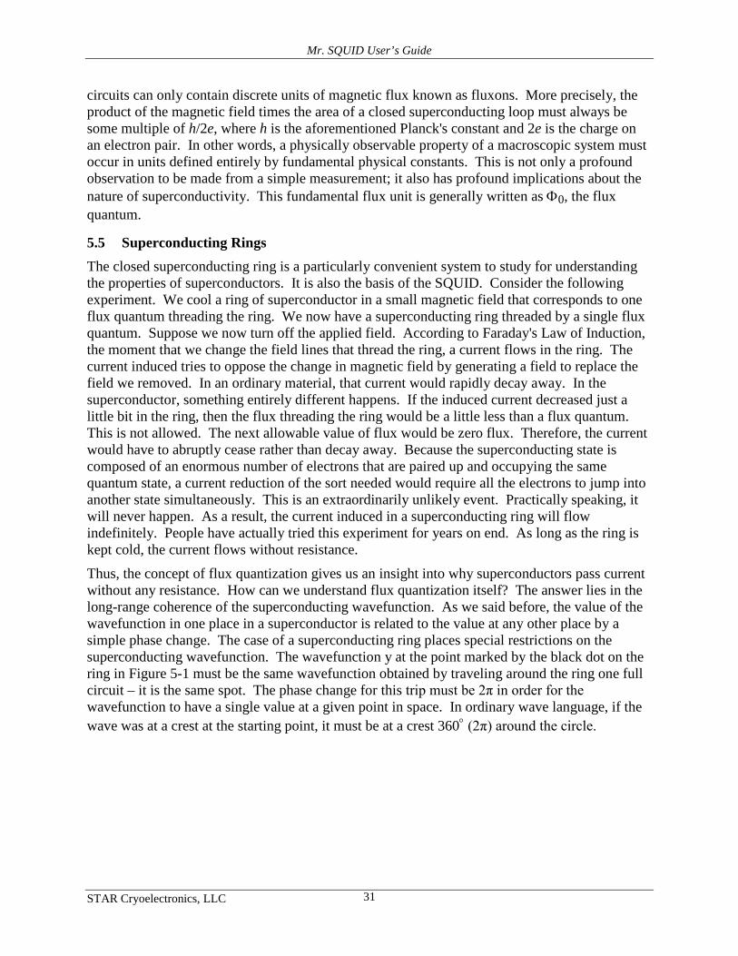
Mr. SQUID User’s Guide
STAR Cryoelectronics, LLC 31
circuits can only contain discrete units of magnetic flux known as fluxons. More precisely, the product of the magnetic field times the area of a closed superconducting loop must always be some multiple of h/2e, where h is the aforementioned Planck's constant and 2e is the charge on an electron pair. In other words, a physically observable property of a macroscopic system must occur in units defined entirely by fundamental physical constants. This is not only a profound observation to be made from a simple measurement; it also has profound implications about the nature of superconductivity. This fundamental flux unit is generally written as Φ0, the flux quantum.
5.5 Superconducting Rings The closed superconducting ring is a particularly convenient system to study for understanding the properties of superconductors. It is also the basis of the SQUID. Consider the following experiment. We cool a ring of superconductor in a small magnetic field that corresponds to one flux quantum threading the ring. We now have a superconducting ring threaded by a single flux quantum. Suppose we now turn off the applied field. According to Faraday's Law of Induction, the moment that we change the field lines that thread the ring, a current flows in the ring. The current induced tries to oppose the change in magnetic field by generating a field to replace the field we removed. In an ordinary material, that current would rapidly decay away. In the superconductor, something entirely different happens. If the induced current decreased just a little bit in the ring, then the flux threading the ring would be a little less than a flux quantum. This is not allowed. The next allowable value of flux would be zero flux. Therefore, the current would have to abruptly cease rather than decay away. Because the superconducting state is composed of an enormous number of electrons that are paired up and occupying the same quantum state, a current reduction of the sort needed would require all the electrons to jump into another state simultaneously. This is an extraordinarily unlikely event. Practically speaking, it will never happen. As a result, the current induced in a superconducting ring will flow indefinitely. People have actually tried this experiment for years on end. As long as the ring is kept cold, the current flows without resistance.
Thus, the concept of flux quantization gives us an insight into why superconductors pass current without any resistance. How can we understand flux quantization itself? The answer lies in the long-range coherence of the superconducting wavefunction. As we said before, the value of the wavefunction in one place in a superconductor is related to the value at any other place by a simple phase change. The case of a superconducting ring places special restrictions on the superconducting wavefunction. The wavefunction y at the point marked by the black dot on the ring in Figure 5-1 must be the same wavefunction obtained by traveling around the ring one full circuit – it is the same spot. The phase change for this trip must be 2π in order for the wavefunction to have a single value at a given point in space. In ordinary wave language, if the wave was at a crest at the starting point, it must be at a crest 360° (2π) around the circle.
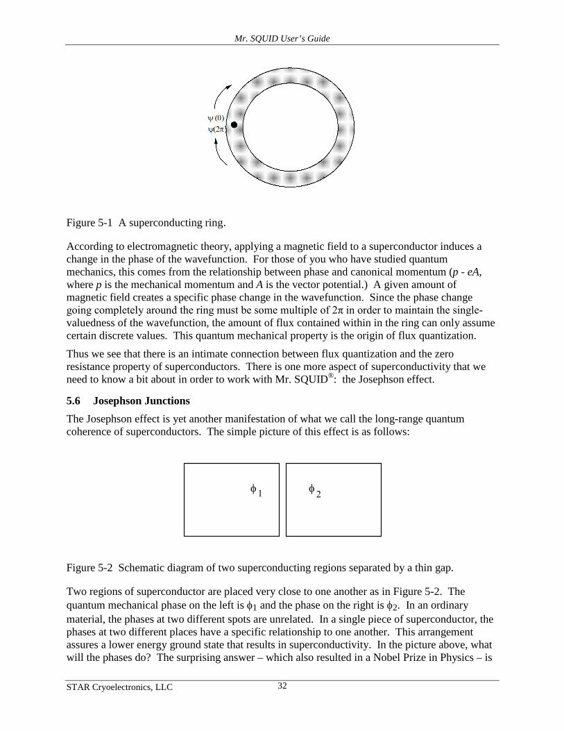
Mr. SQUID User’s Guide
STAR Cryoelectronics, LLC 32
Figure 5-1 A superconducting ring.
According to electromagnetic theory, applying a magnetic field to a superconductor induces a change in the phase of the wavefunction. For those of you who have studied quantum mechanics, this comes from the relationship between phase and canonical momentum (p - eA, where p is the mechanical momentum and A is the vector potential.) A given amount of magnetic field creates a specific phase change in the wavefunction. Since the phase change going completely around the ring must be some multiple of 2π in order to maintain the single-valuedness of the wavefunction, the amount of flux contained within in the ring can only assume certain discrete values. This quantum mechanical property is the origin of flux quantization.
Thus we see that there is an intimate connection between flux quantization and the zero resistance property of superconductors. There is one more aspect of superconductivity that we need to know a bit about in order to work with Mr. SQUID®: the Josephson effect.
5.6 Josephson Junctions The Josephson effect is yet another manifestation of what we call the long-range quantum coherence of superconductors. The simple picture of this effect is as follows:
φ φ1 2
Figure 5-2 Schematic diagram of two superconducting regions separated by a thin gap.
Two regions of superconductor are placed very close to one another as in Figure 5-2. The quantum mechanical phase on the left is φ1 and the phase on the right is φ2. In an ordinary material, the phases at two different spots are unrelated. In a single piece of superconductor, the phases at two different places have a specific relationship to one another. This arrangement assures a lower energy ground state that results in superconductivity. In the picture above, what will the phases do? The surprising answer – which also resulted in a Nobel Prize in Physics – is
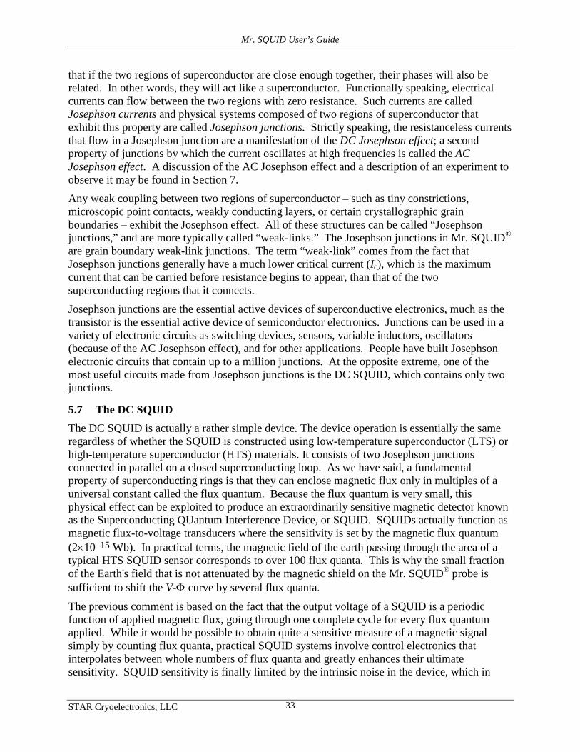
Mr. SQUID User’s Guide
STAR Cryoelectronics, LLC 33
that if the two regions of superconductor are close enough together, their phases will also be related. In other words, they will act like a superconductor. Functionally speaking, electrical currents can flow between the two regions with zero resistance. Such currents are called Josephson currents and physical systems composed of two regions of superconductor that exhibit this property are called Josephson junctions. Strictly speaking, the resistanceless currents that flow in a Josephson junction are a manifestation of the DC Josephson effect; a second property of junctions by which the current oscillates at high frequencies is called the AC Josephson effect. A discussion of the AC Josephson effect and a description of an experiment to observe it may be found in Section 7. Any weak coupling between two regions of superconductor – such as tiny constrictions, microscopic point contacts, weakly conducting layers, or certain crystallographic grain boundaries – exhibit the Josephson effect. All of these structures can be called “Josephson junctions,” and are more typically called “weak-links.” The Josephson junctions in Mr. SQUID® are grain boundary weak-link junctions. The term “weak-link” comes from the fact that Josephson junctions generally have a much lower critical current (Ic), which is the maximum current that can be carried before resistance begins to appear, than that of the two superconducting regions that it connects.
Josephson junctions are the essential active devices of superconductive electronics, much as the transistor is the essential active device of semiconductor electronics. Junctions can be used in a variety of electronic circuits as switching devices, sensors, variable inductors, oscillators (because of the AC Josephson effect), and for other applications. People have built Josephson electronic circuits that contain up to a million junctions. At the opposite extreme, one of the most useful circuits made from Josephson junctions is the DC SQUID, which contains only two junctions.
5.7 The DC SQUID The DC SQUID is actually a rather simple device. The device operation is essentially the same regardless of whether the SQUID is constructed using low-temperature superconductor (LTS) or high-temperature superconductor (HTS) materials. It consists of two Josephson junctions connected in parallel on a closed superconducting loop. As we have said, a fundamental property of superconducting rings is that they can enclose magnetic flux only in multiples of a universal constant called the flux quantum. Because the flux quantum is very small, this physical effect can be exploited to produce an extraordinarily sensitive magnetic detector known as the Superconducting QUantum Interference Device, or SQUID. SQUIDs actually function as magnetic flux-to-voltage transducers where the sensitivity is set by the magnetic flux quantum (2×10–15 Wb). In practical terms, the magnetic field of the earth passing through the area of a typical HTS SQUID sensor corresponds to over 100 flux quanta. This is why the small fraction of the Earth's field that is not attenuated by the magnetic shield on the Mr. SQUID® probe is sufficient to shift the V-Φ curve by several flux quanta.
The previous comment is based on the fact that the output voltage of a SQUID is a periodic function of applied magnetic flux, going through one complete cycle for every flux quantum applied. While it would be possible to obtain quite a sensitive measure of a magnetic signal simply by counting flux quanta, practical SQUID systems involve control electronics that interpolates between whole numbers of flux quanta and greatly enhances their ultimate sensitivity. SQUID sensitivity is finally limited by the intrinsic noise in the device, which in
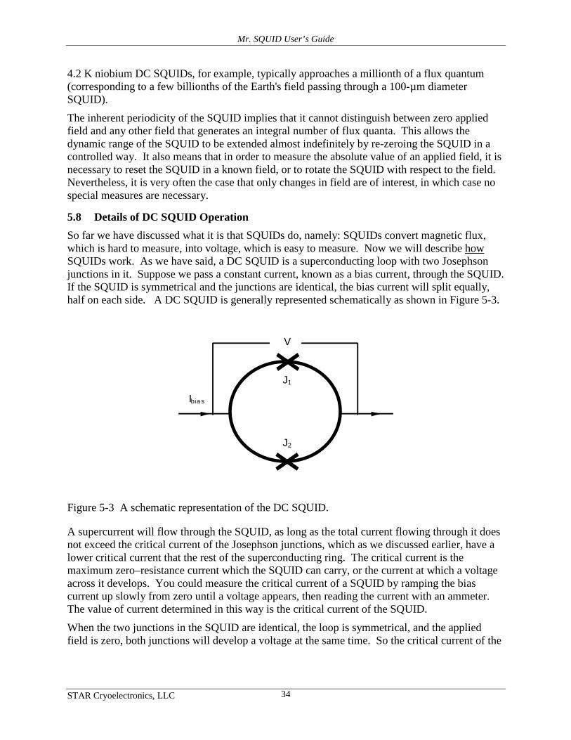
Mr. SQUID User’s Guide
STAR Cryoelectronics, LLC 34
4.2 K niobium DC SQUIDs, for example, typically approaches a millionth of a flux quantum (corresponding to a few billionths of the Earth's field passing through a 100-µm diameter SQUID).
The inherent periodicity of the SQUID implies that it cannot distinguish between zero applied field and any other field that generates an integral number of flux quanta. This allows the dynamic range of the SQUID to be extended almost indefinitely by re-zeroing the SQUID in a controlled way. It also means that in order to measure the absolute value of an applied field, it is necessary to reset the SQUID in a known field, or to rotate the SQUID with respect to the field. Nevertheless, it is very often the case that only changes in field are of interest, in which case no special measures are necessary.
5.8 Details of DC SQUID Operation So far we have discussed what it is that SQUIDs do, namely: SQUIDs convert magnetic flux, which is hard to measure, into voltage, which is easy to measure. Now we will describe how SQUIDs work. As we have said, a DC SQUID is a superconducting loop with two Josephson junctions in it. Suppose we pass a constant current, known as a bias current, through the SQUID. If the SQUID is symmetrical and the junctions are identical, the bias current will split equally, half on each side. A DC SQUID is generally represented schematically as shown in Figure 5-3.
Ibia s
V
J1
J2
Figure 5-3 A schematic representation of the DC SQUID.
A supercurrent will flow through the SQUID, as long as the total current flowing through it does not exceed the critical current of the Josephson junctions, which as we discussed earlier, have a lower critical current that the rest of the superconducting ring. The critical current is the maximum zero–resistance current which the SQUID can carry, or the current at which a voltage across it develops. You could measure the critical current of a SQUID by ramping the bias current up slowly from zero until a voltage appears, then reading the current with an ammeter. The value of current determined in this way is the critical current of the SQUID.
When the two junctions in the SQUID are identical, the loop is symmetrical, and the applied field is zero, both junctions will develop a voltage at the same time. So the critical current of the
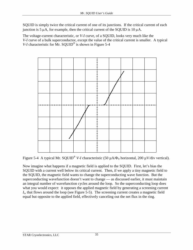
Mr. SQUID User’s Guide
STAR Cryoelectronics, LLC 35
SQUID is simply twice the critical current of one of its junctions. If the critical current of each junction is 5 µA, for example, then the critical current of the SQUID is 10 µA.
The voltage-current characteristic, or V-I curve, of a SQUID, looks very much like the V-I curve of a bulk superconductor, except the value of the critical current is smaller. A typical V-I characteristic for Mr. SQUID® is shown in Figure 5-4
Figure 5-4 A typical Mr. SQUID® V-I characteristic (50 µA/Φ0 horizontal, 200 µV/div vertical).
Now imagine what happens if a magnetic field is applied to the SQUID. First, let’s bias the SQUID with a current well below its critical current. Then, if we apply a tiny magnetic field to the SQUID, the magnetic field wants to change the superconducting wave function. But the superconducting wavefunction doesn’t want to change — as discussed earlier, it must maintain an integral number of wavefunction cycles around the loop. So the superconducting loop does what you would expect: it opposes the applied magnetic field by generating a screening current Is, that flows around the loop (see Figure 5-5). The screening current creates a magnetic field equal but opposite to the applied field, effectively canceling out the net flux in the ring.
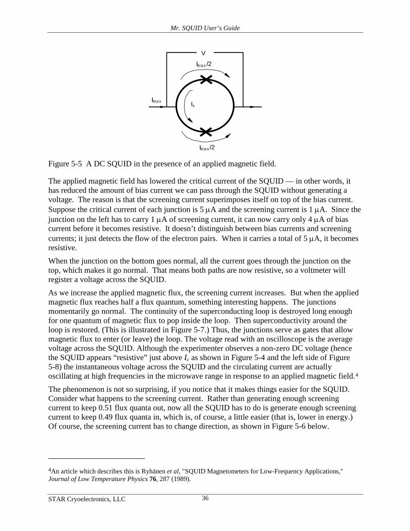
Mr. SQUID User’s Guide
STAR Cryoelectronics, LLC 36
Ibia s
V
Ibia s /2
Ibia s /2
Is
Figure 5-5 A DC SQUID in the presence of an applied magnetic field.
The applied magnetic field has lowered the critical current of the SQUID — in other words, it has reduced the amount of bias current we can pass through the SQUID without generating a voltage. The reason is that the screening current superimposes itself on top of the bias current. Suppose the critical current of each junction is 5 µA and the screening current is 1 µA. Since the junction on the left has to carry 1 µA of screening current, it can now carry only 4 µA of bias current before it becomes resistive. It doesn’t distinguish between bias currents and screening currents; it just detects the flow of the electron pairs. When it carries a total of 5 µA, it becomes resistive.
When the junction on the bottom goes normal, all the current goes through the junction on the top, which makes it go normal. That means both paths are now resistive, so a voltmeter will register a voltage across the SQUID.
As we increase the applied magnetic flux, the screening current increases. But when the applied magnetic flux reaches half a flux quantum, something interesting happens. The junctions momentarily go normal. The continuity of the superconducting loop is destroyed long enough for one quantum of magnetic flux to pop inside the loop. Then superconductivity around the loop is restored. (This is illustrated in Figure 5-7.) Thus, the junctions serve as gates that allow magnetic flux to enter (or leave) the loop. The voltage read with an oscilloscope is the average voltage across the SQUID. Although the experimenter observes a non-zero DC voltage (hence the SQUID appears “resistive” just above Ic as shown in Figure 5-4 and the left side of Figure 5-8) the instantaneous voltage across the SQUID and the circulating current are actually oscillating at high frequencies in the microwave range in response to an applied magnetic field.4
The phenomenon is not so surprising, if you notice that it makes things easier for the SQUID. Consider what happens to the screening current. Rather than generating enough screening current to keep 0.51 flux quanta out, now all the SQUID has to do is generate enough screening current to keep 0.49 flux quanta in, which is, of course, a little easier (that is, lower in energy.) Of course, the screening current has to change direction, as shown in
Figure 5-6 below.
4An article which describes this is Ryhänen et al, "SQUID Magnetometers for Low-Frequency Applications," Journal of Low Temperature Physics 76, 287 (1989).
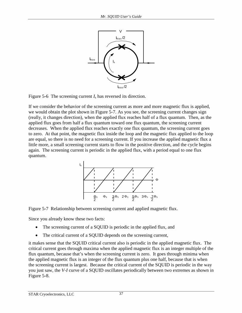
Mr. SQUID User’s Guide
STAR Cryoelectronics, LLC 37
Ibia s
V
Ibia s /2
Ibia s /2
Is
Figure 5-6 The screening current Is has reversed its direction.
If we consider the behavior of the screening current as more and more magnetic flux is applied, we would obtain the plot shown in Figure 5-7. As you see, the screening current changes sign (really, it changes direction), when the applied flux reaches half of a flux quantum. Then, as the applied flux goes from half a flux quantum toward one flux quantum, the screening current decreases. When the applied flux reaches exactly one flux quantum, the screening current goes to zero. At that point, the magnetic flux inside the loop and the magnetic flux applied to the loop are equal, so there is no need for a screening current. If you increase the applied magnetic flux a little more, a small screening current starts to flow in the positive direction, and the cycle begins again. The screening current is periodic in the applied flux, with a period equal to one flux quantum.
Is
Φ
2 2 2 2 7 5 3 2 3 Φ0 Φ0 Φ0 Φ0 Φ0 Φ0 Φ0
Figure 5-7 Relationship between screening current and applied magnetic flux.
Since you already know these two facts:
• The screening current of a SQUID is periodic in the applied flux, and
• The critical current of a SQUID depends on the screening current, it makes sense that the SQUID critical current also is periodic in the applied magnetic flux. The critical current goes through maxima when the applied magnetic flux is an integer multiple of the flux quantum, because that’s when the screening current is zero. It goes through minima when the applied magnetic flux is an integer of the flux quantum plus one half, because that is when the screening current is largest. Because the critical current of the SQUID is periodic in the way you just saw, the V-I curve of a SQUID oscillates periodically between two extremes as shown in Figure 5-8.
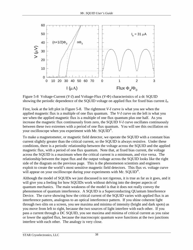
Mr. SQUID User’s Guide
STAR Cryoelectronics, LLC 38
I (µΑ)
0 10 20 30 40 50 60 70
V (µ
V)
0
10
20
30
40
50
60
Flux Φa/Φ0
0 1 2 3
nΦ0(n+1/2)Φ0
Ib = 31 µA
Figure 5-8 Voltage-Current (V-I) and Voltage-Flux (V-Φ) characteristics of a dc SQUID showing the periodic dependence of the SQUID voltage on applied flux for fixed bias current Ib.
First, look at the left plot in Figure 5-8. The rightmost V-I curve is what you see when the applied magnetic flux is a multiple of one flux quantum. The V-I curve on the left is what you see when the applied magnetic flux is a multiple of one flux quantum plus one half. As you increase the magnetic flux continuously from zero, the SQUID V-I curve oscillates continuously between these two extremes with a period of one flux quantum. You will see this oscillation on your oscilloscope when you experiment with Mr. SQUID®.
To make a magnetometer, or magnetic field detector, we operate the SQUID with a constant bias current slightly greater than the critical current, so the SQUID is always resistive. Under these conditions, there is a periodic relationship between the voltage across the SQUID and the applied magnetic flux, with a period of one flux quantum. Note that, at fixed bias current, the voltage across the SQUID is a maximum when the critical current is a minimum, and vice versa. The relationship between the input flux and the output voltage across the SQUID looks like the right side of the diagram on the previous page. This is the phenomenon scientists and engineers exploit to create the world’s most sensitive magnetic field detectors. This flux vs. voltage curve will appear on your oscilloscope during your experiments with Mr. SQUID®.
Although the model of SQUIDs we just discussed is not rigorous, it is true as far as it goes, and it will give you a feeling for how SQUIDs work without delving into the deeper aspects of quantum mechanics. The main weakness of the model is that it does not really convey the phenomenon of quantum interference. A SQUID is a Superconducting QUantum Interference Device. The curve showing how the critical current of the SQUID varies with applied flux is an interference pattern, analogous to an optical interference pattern. If you shine coherent light through two slits on a screen, you see maxima and minima of intensity (bright and dark spots) as you move from left to right, because the two sources of light interfere with each other. If you pass a current through a DC SQUID, you see maxima and minima of critical current as you raise or lower the applied flux, because the macroscopic quantum wave functions at the two junctions interfere with each other. The analogy is very close.
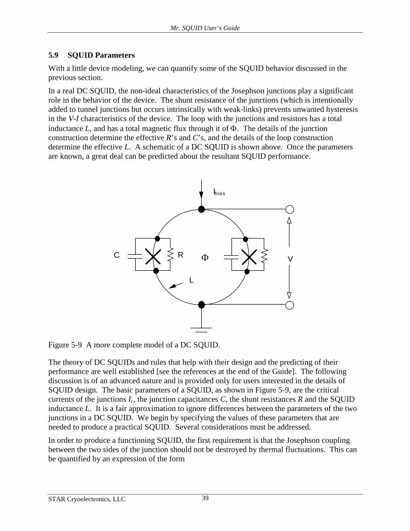
Mr. SQUID User’s Guide
STAR Cryoelectronics, LLC 39
5.9 SQUID Parameters With a little device modeling, we can quantify some of the SQUID behavior discussed in the previous section.
In a real DC SQUID, the non-ideal characteristics of the Josephson junctions play a significant role in the behavior of the device. The shunt resistance of the junctions (which is intentionally added to tunnel junctions but occurs intrinsically with weak-links) prevents unwanted hysteresis in the V-I characteristics of the device. The loop with the junctions and resistors has a total inductance L, and has a total magnetic flux through it of Φ. The details of the junction construction determine the effective R’s and C’s, and the details of the loop construction determine the effective L. A schematic of a DC SQUID is shown above. Once the parameters are known, a great deal can be predicted about the resultant SQUID performance.
Ibia s
V
Φ R C
L
Figure 5-9 A more complete model of a DC SQUID.
The theory of DC SQUIDs and rules that help with their design and the predicting of their performance are well established [see the references at the end of the Guide]. The following discussion is of an advanced nature and is provided only for users interested in the details of SQUID design. The basic parameters of a SQUID, as shown in Figure 5-9, are the critical currents of the junctions Ic, the junction capacitances C, the shunt resistances R and the SQUID inductance L. It is a fair approximation to ignore differences between the parameters of the two junctions in a DC SQUID. We begin by specifying the values of these parameters that are needed to produce a practical SQUID. Several considerations must be addressed.
In order to produce a functioning SQUID, the first requirement is that the Josephson coupling between the two sides of the junction should not be destroyed by thermal fluctuations. This can be quantified by an expression of the form
Mr. SQUID User’s Guide
STAR Cryoelectronics, LLC 40
Eqn. 5-1 TkI
Bc 52
0 >πΦ ,
where kB is Boltzman’s constant (kB = 1.38 × 10⁻²³ Joule/K). This determines a desirable minimum value for Ic. The second requirement is that thermal fluctuations in the flux in the SQUID should not exceed a fraction of a flux quantum. This can be quantified in the following form:
Eqn. 5-2 TkL B
L 52
>Φ ,
which puts an upper limit on the inductance of the SQUID. The unavoidable capacitance of any junction tends to make its current-voltage characteristic hysteretic. This complication can be avoided by making the shunt resistance small enough. This condition can be met by limiting the value of a parameter known as the “McCumber parameter” βc, given by:
Eqn. 5-3 12
0
2
<Φ
π=β
CRIcc
For βc < 0.7, the junctions are non-hysteretic, and this fixes the maximum resistance that can be used for a given capacitance and critical current. This capacitance is usually determined, for a particular junction technology, once the critical current has been set. The final design parameter is the modulation parameter defined by the expression
Eqn. 5-4 0
2Φ
=β cL
LI
This parameter determines the maximum extent to which circulating current in the SQUID can shield the applied flux, and is a factor in determining the flux-to-voltage transfer ratio of the SQUID. In Section 3of the User's Guide, two procedures for determining this parameter for the SQUID in the Mr. SQUID® system are outlined.
In addition to these theoretical parameters, there are some restrictions that are determined by the superconducting technology used in the SQUID. In the case of the YBCO grain boundary junctions used in Mr. SQUID®, the most important restriction arises from the fact that, as well as allowing Cooper pairs to pass, the junctions also allow a large current of single electrons to pass. This current behaves like the current that would flow through an intentionally added parallel resistor. One consequence is that the condition on βc is always satisfied: the junctions are not hysteretic. A less welcome consequence is that the product IcRN is a constant determined by the nature of the grain boundary (and the temperature). The size of IcRN is important because, along with βL, it determines the voltage that the SQUID generates in response to a change in flux. It has been shown [see the reference by Tesche and Clarke] that, at the optimum bias current, the
Mr. SQUID User’s Guide
STAR Cryoelectronics, LLC 41
change in SQUID voltage when the applied flux changes from zero to Φ0/2 is approximated by the expression5
Eqn. 5-5
( )L
NcRIVβπ +
=∆1
4
Extensive calculations and experiments have shown that a value of βL ≈ 1 is a good choice for low noise operation.
In the Mr. SQUID® experiments, it is possible to calculate βL using the measured values of Ic and L and Eqn. 3-1. Then, one may compare the predicted voltage modulation using Eqn. 5-5 and Eqn. 3-5 with the value determined experimentally.
5.10 SQUID Operation If a bias current less than the junction critical current is injected through the loop, then, as a consequence of the DC Josephson effect, there will be no voltage across the loop. If the bias current is raised above this critical current, then a voltage develops across the loop. The critical current Ic(Φ) is also a function of the magnetic flux through the loop and may be expressed as
Eqn. 5-6
Φ
Φπ=Φ
0
cos)0()( cc II
where Φ0 = h/2e = 2.07×10⁻¹⁵ Wb, the magnetic flux quantum, and this leads to the V-Φ characteristic shown in Figure 5-8. The total measured current is Itotal(Φ) = Ic(Φ) + Ileakage, where Ileakage is the leakage current through resistors of Figure 5-9. So, if the magnetic flux through the loop is changed, the critical current is changed and the non-linear voltage-current behavior of the loop is altered. Note that this equation is identical in form to the equation describing quantum interference of light diffracted by two slits, which displays an interference pattern between wave fronts that pass through the different slits. By analogy, the behavior of this double Josephson junction loop displays interference in the current-voltage behavior as magnetic flux threads the loop, hence the name Superconducting QUantum Interference Device, SQUID.
One does not need to measure a whole period in the SQUID modulation to perform a flux measurement. One can measure quite accurately a small fraction of a period, and detect changes in the flux threading the SQUID loop that are much smaller than a flux quantum, Φ0. A SQUID biased to where ∂V/∂Φ is maximized produces a considerable output voltage in response to a small input flux dΦ, thus acting as a magnetic flux-to-voltage converter.
One usually uses a SQUID in a flux-locked mode, where an external coil is used to generate a magnetic field in such a manner as to keep the total flux through the SQUID loop constant. The current supplied to this coil is used to indicate the value of the unknown flux being canceled. Thus the flux measurement is manifested as a current measurement that can be performed with extremely high sensitivity and accuracy, and also has the additional advantage of large dynamic
5 This equation is obtained by solving Eqn. 3-2 for ∆V. If thermal effects are to be considered as in the case of a high-Tc SQUID, then Eqn. 3-5 is used.
Mr. SQUID User’s Guide
STAR Cryoelectronics, LLC 42
range in magnetic field measurements. It is possible to use Mr. SQUID® in this way, and this is detailed in the Advanced Experiments in Section 7.
5.11 Practical SQUID Magnetometers Although in some applications it is convenient to expose the SQUID directly to the magnetic field of interest, more often the magnetic signal is conveyed to the SQUID by a flux transformer. A flux transformer is a closed superconducting circuit consisting of two coils in series. We emphasize that a SQUID flux transformer is superconducting because that means it can be used to couple static fields (ω = 0) as well as the alternating (ω > 0) fields that a non-superconducting transformer can couple. One coil, the input coil, is magnetically coupled to the SQUID and is usually fabricated along with it; the second or pick-up coil is exposed to the field to be measured. This second coil acts as a magnetic antenna that couples external signals into the SQUID. It is a basic principle of superconductivity that the flux inside a closed superconducting circuit cannot change. Consequently, a change in field that causes the flux in the pick-up coil to change also causes a change in the flux in the input coil. The SQUID senses this latter flux change. The area of the pick–up coil is usually much greater than the area of the SQUID. The prime function of the transformer is to convert the high magnetic flux sensitivity of the SQUID itself into a high magnetic field sensitivity.
Another advantage of using a flux transformer is that the input coil, which can be made as a wire or a thin film structure, can be configured to suit the measurement at hand. In particular, it can be wound so as to be sensitive not to the magnetic field itself, but to the gradient of the field in a chosen direction, or to a higher derivative of the field. In these cases the flux transformer is referred to as a gradiometer. Since the gradient of the magnetic field falls off more rapidly with distance from the magnetic source than the field itself, a gradiometer tends to reject magnetic interference from distant sources, while remaining sensitive to closer objects. Again, a gradiometer is basically sensitive to changes in the field gradient rather than its absolute value, and the technique of controlled resetting can be applied to give a large dynamic range.
The connections to the coils in Mr. SQUID® are not made of superconducting material, so that one cannot couple a superconducting flux transformer to it. This limitation comes from economics and simplicity of operation for the Mr. SQUID® product. As a result, external static flux cannot be coupled directly to Mr. SQUID® though an external pickup loop.
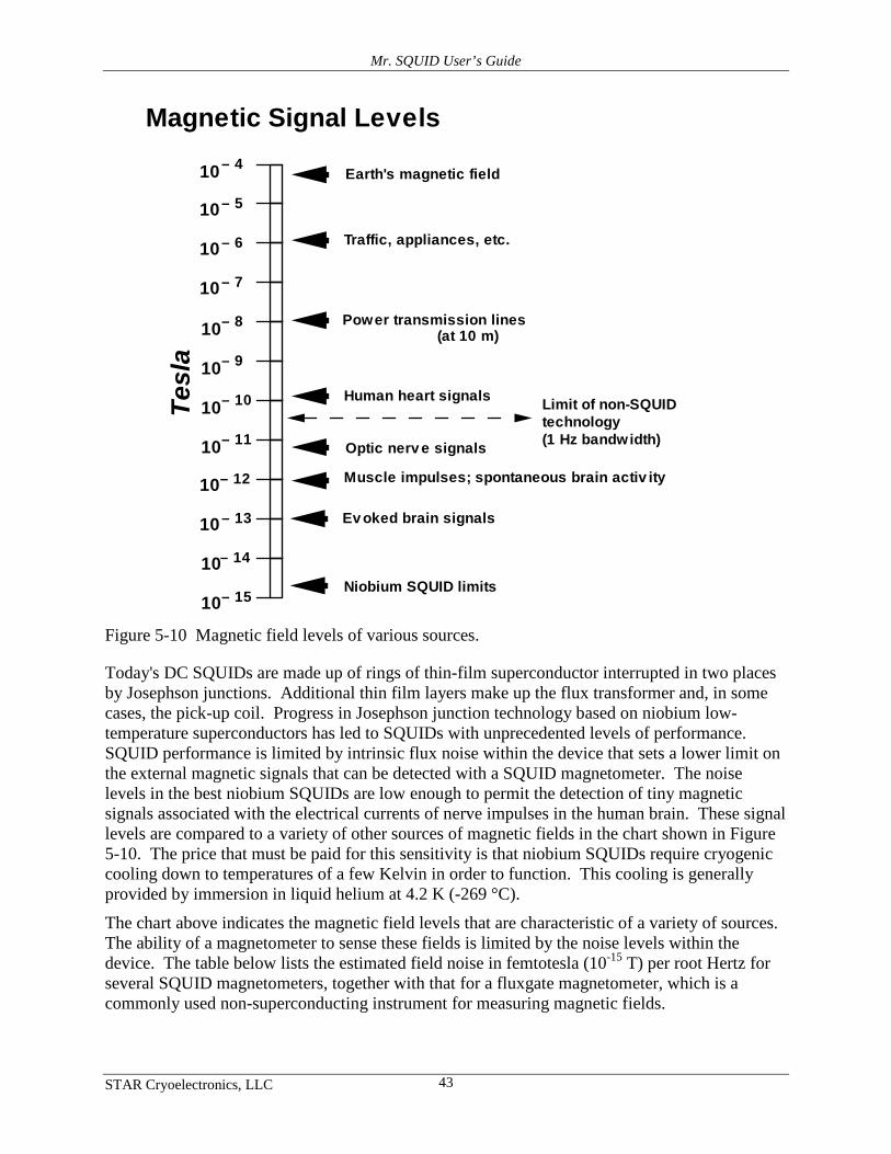
Mr. SQUID User’s Guide
STAR Cryoelectronics, LLC 43
Tesl
a10
10
10
10
10
10
10
10
10
10
10
10
– 4
– 5
– 6
– 7
– 8
– 9
– 10
– 11
– 12
– 13
– 14
– 15
Earth's magnetic field
Traffic, appliances, etc.
Power transmission lines
Human heart signals
Optic nerv e signals
Muscle impulses; spontaneous brain activ ity
Ev oked brain signals
Niobium SQUID limits
Magnetic Signal Levels
(at 10 m)
Limit of non-SQUID technology (1 Hz bandwidth)
Figure 5-10 Magnetic field levels of various sources.
Today's DC SQUIDs are made up of rings of thin-film superconductor interrupted in two places by Josephson junctions. Additional thin film layers make up the flux transformer and, in some cases, the pick-up coil. Progress in Josephson junction technology based on niobium low-temperature superconductors has led to SQUIDs with unprecedented levels of performance. SQUID performance is limited by intrinsic flux noise within the device that sets a lower limit on the external magnetic signals that can be detected with a SQUID magnetometer. The noise levels in the best niobium SQUIDs are low enough to permit the detection of tiny magnetic signals associated with the electrical currents of nerve impulses in the human brain. These signal levels are compared to a variety of other sources of magnetic fields in the chart shown in Figure 5-10. The price that must be paid for this sensitivity is that niobium SQUIDs require cryogenic cooling down to temperatures of a few Kelvin in order to function. This cooling is generally provided by immersion in liquid helium at 4.2 K (-269 °C).
The chart above indicates the magnetic field levels that are characteristic of a variety of sources. The ability of a magnetometer to sense these fields is limited by the noise levels within the device. The table below lists the estimated field noise in femtotesla (10-15 T) per root Hertz for several SQUID magnetometers, together with that for a fluxgate magnetometer, which is a commonly used non-superconducting instrument for measuring magnetic fields.
Mr. SQUID User’s Guide
STAR Cryoelectronics, LLC 44
Sensor Field Noise in fT/Hz½ At 1 Hz At 100 Hz
Flux Gate (room temperature) 30,000 30,000
77 K YBCO DC SQUID Magnetometer <100 <40
4.2 K Nb DC SQUID Magnetometer <5 <4
5.12 SQUID Applications Liquid-helium-cooled SQUIDs have been commercial products for two decades. In the early stages, the primary uses for these devices were in laboratory instrumentation. Generally speaking, technically trained users such as physicists and electrical engineers used commercial SQUIDs as highly sensitive magnetic field detectors, voltmeters, or null detectors for experiments that were already being conducted at cryogenic temperatures. During the past decade, however, complete instruments have become available that incorporate helium-temperature SQUIDs that require less expertise on the part of the user. The prime example of this type of application is the SQUID susceptometer that is widely used by many laboratory scientists. Ironically, this instrument has found its greatest application in the study of material properties of high-temperature superconductors. Other examples include rock magnetometers that analyze the magnetic properties of mineral samples. These SQUID-based instruments feature liquid helium dewars with hold times greater than one year! Clearly, for at least some fixed installations, liquid helium does not impose great hardships.
Special-purpose SQUID instruments for users other than laboratory scientists have been slower to reach the marketplace. The main example in this category is the multi-channel SQUID-based system for biomedical applications. Several companies worldwide market systems of this kind, which sell for as much as $3 million. The two main applications are magnetoencephalography (MEG) and magnetocardiography (MCG), in which the magnetometers measure magnetic signals generated in the brain and heart, respectively. The SQUID system is contactless and may yield additional or complementary information to the conventional electroencephalogram (EEG) or electrocardiogram (EKG). There are a number of applications beyond MEG and MCG that make use of SQUIDs. The combination of SQUIDs and superconducting magnets can be used as a “magneto-ferritometer,” which is a specialized instrument used to monitor iron levels in the liver. This is an important diagnostic tool for identifying a condition known as hemochromatosis, which can be extremely serious if not detected.
In addition to the commercial marketplace, there has been considerable development effort on a variety of SQUID applications for the military. The U.S. Navy has sponsored research for many years on SQUIDs for submarine and mine detection in both airborne and ocean-going platforms. For this application, the remote fielding and demanding environment for the system are major barriers to the use of liquid-helium-cooled SQUIDs. Nitrogen cooling offers a far more viable alternative if HTS SQUID performance can meet the requirements of this application.
A number of applications have been investigated in the area of geophysics. These range from prospecting for oil and minerals to earthquake prediction. There are a variety of different techniques that have been explored that use of SQUIDs. Active systems introduce pulsed magnetic signals into the earth and then detect the response by means of the SQUID. One
Mr. SQUID User’s Guide
STAR Cryoelectronics, LLC 45
version of this technique is essentially a type of NMR that determines the properties of the different strata that make up the ground in a test site. Currently, conventional (i.e. non-SQUID) magnetometers are used for “bore-hole logging,” an important technique for locating oil.
An important passive geophysical technique that utilizes SQUIDs is known as magnetotellurics. In this technique, the properties of an area of ground (actually the impedance tensor of the ground) are determined by comparing the signals at a reference SQUID to those at a test SQUID that is moved from point to point. During the early 1980’s, several companies practiced this technique on a commercial basis. However, the subsequent drop in the cost of oil –– and the removal of incentives to develop alternative energy sources, such as geothermal energy –– ended the commercial viability of such surveying techniques. As in the case of the magnetic anomaly detection applications, remote magnetic field measurement is a critical issue for geophysical applications and, therefore, HTS SQUIDs represent a significant advance in practicality.
Another area of investigation has been non-destructive evaluation (NDE) using SQUIDs. Once again, there are a variety of proposed techniques and implementations, both active and passive. Of special interest is the testing of submerged or otherwise inaccessible pipes, the evaluation of structural members such as bridge components, the location of buried toxic waste drums, and the testing of welds in structures such as aircraft wings. Initial studies indicate that SQUIDs may be effective in all these areas, but considerable modeling and testing remains to be done to demonstrate the viability of the method.
In summary, there is a great variety of SQUID applications either under investigation or commercially available. What has kept the majority of them out of the marketplace is a combination of the difficulties imposed by cryogenic requirements and the lack of sufficient demonstration of their utility. As high-temperature superconductor-based SQUIDs alleviate the former problem, the opportunities to eliminate the latter problem will only increase. The Mr. SQUID® system before you represented the first step in bringing HTS SQUID technology into the marketplace.
5.13 A Brief History of SQUIDs The quantum interference between two Josephson tunnel junctions was first reported by Jaklevic, Lambe, Silver, and Mercereau in early 1964, roughly a year after the first observation of Josephson tunneling by Anderson and Rowell. In both of these experiments, the authors used tunnel junctions consisting of two thin superconducting films separated by an oxide layer roughly 20 Å thick. However, at the time tunnel junctions were difficult to make reproducibly and usually did not cycle reliably between room temperature and liquid helium temperatures. For this reason, virtually all the device development over the ensuing decade involved devices made from bulk superconductors rather than thin films.
Much progress was made with SQUIDs involving point contact junctions consisting of sharpened niobium screws, often adjustable from the top of the cryostat, pressed against a block of niobium. Another device, the SLUG (Superconducting Low-inductance Undulating Galvanometer) consisted of a bead of tin-lead solder frozen around a length of niobium wire. Supercurrents flowed between the solder and the wire at a few discrete points only, and the critical current of the device was modulated by a current passed along the wire.
A major change occurred in the late 1960’s, however, with the advent of the rf SQUID, a closed superconducting loop interrupted by a single Josephson junction. The rf SQUID is inductively
Mr. SQUID User’s Guide
STAR Cryoelectronics, LLC 46
coupled to an inductor in parallel with a capacitor and the circuit is excited by an external oscillator at its resonant frequency, typically 30 MHz. The amplitude of the rf signal across the tank circuit turns out to be periodic in the flux applied to the SQUID – the period (of course!) is Φ0 – so that by monitoring this amplitude with suitable electronics one can measure small changes in magnetic flux in much the same way as for the DC SQUID. At the time, a major advantage of the rf SQUID over the DC SQUID was the fact that it required only a single Josephson junction. The rf SQUID – with a point contact junction – became commercially available in the early 1970's by S.H.E. in San Diego, CA, and has had a long history of successful use. It is undoubtedly true that, until very recently, more physics experiments were carried out with the rf SQUID than with the DC SQUID for the simple reason that only the former was commercially available.
The next major step in the development of SQUIDs was the introduction of the thin film DC SQUID in 1976. This device, built on a cylindrical quartz tube and involving Nb-NbOx-PbIn tunnel junctions, offered a major advance in resolution. This improvement was due partly to the use of ideal junctions and partly to the optimal coupling of the SQUID to the room temperature electronics via a cooled resonant circuit. Shortly afterwards a comprehensive theory for the white noise in the DC SQUID demonstrated that “smaller is better,” spurring the development of photolithographically processed devices.
The type of DC SQUID most commonly used today is the square washer configuration first produced in 1982. In this design, the thin-film body of the SQUID is covered with a thin insulating layer on top of which is grown a thin film spiral coil with as many as 50 turns. This scheme produces very tight inductive coupling between the coil and the SQUID. Devices of this kind – with niobium superconducting films used throughout – can be made in batches of as many as a thousand or more at a time on silicon wafers.
The development of SQUIDs – like all other aspects of superconductivity – received a tremendous boost from the advent of high-temperature superconductivity in 1986. Within a few months of the first thin film depositions, HTS DC SQUIDs had been announced, with junctions consisting of randomly-occurring boundaries between superconducting grains in the films. Despite the apparent crudity of these devices (somewhat reminiscent of the early days of LTS SQUIDs), much progress has been made in understanding their behavior and noise limitations. More recently, more controlled junctions have been developed, enabling one to produce DC SQUIDs with relatively predictable characteristics. Your Mr. SQUID® chip is the first commercialization of this technology.
5.14 The SQUID in Mr. SQUID® The SQUID in the Mr. SQUID® probe is a thin film of YBCO superconductor broken in two places by Josephson junctions. Because most of the magnetic flux generated by either of the Mr. SQUID® feedback coils (see Figure 3-8) is forced into the center hole of the SQUID owing to the Meissner Effect, the inductive coupling of each coil to the SQUID is similar, even though their physical sizes are different. This flux-focusing effect enhances the coupling of multi-turn spiral coils that can be fabricated on top of the SQUID body, with each turn contributing roughly the same amount of flux.
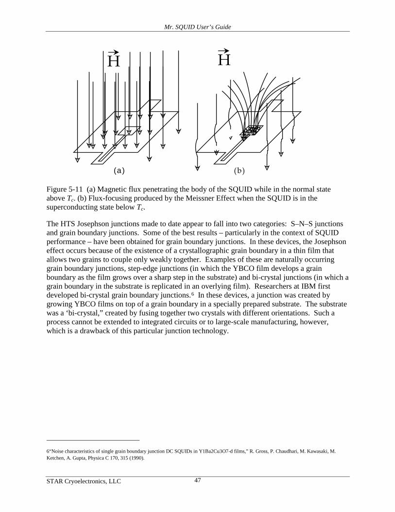
Mr. SQUID User’s Guide
STAR Cryoelectronics, LLC 47
(a) (b)
HH
Figure 5-11 (a) Magnetic flux penetrating the body of the SQUID while in the normal state above Tc. (b) Flux-focusing produced by the Meissner Effect when the SQUID is in the superconducting state below Tc.
The HTS Josephson junctions made to date appear to fall into two categories: S–N–S junctions and grain boundary junctions. Some of the best results – particularly in the context of SQUID performance – have been obtained for grain boundary junctions. In these devices, the Josephson effect occurs because of the existence of a crystallographic grain boundary in a thin film that allows two grains to couple only weakly together. Examples of these are naturally occurring grain boundary junctions, step-edge junctions (in which the YBCO film develops a grain boundary as the film grows over a sharp step in the substrate) and bi-crystal junctions (in which a grain boundary in the substrate is replicated in an overlying film). Researchers at IBM first developed bi-crystal grain boundary junctions.6
6“Noise characteristics of single grain boundary junction DC SQUIDs in Y1Ba2Cu3O7-d films,” R. Gross, P. Chaudhari, M. Kawasaki, M. Ketchen, A. Gupta, Physica C 170, 315 (1990).
In these devices, a junction was created by growing YBCO films on top of a grain boundary in a specially prepared substrate. The substrate was a ‘bi-crystal,” created by fusing together two crystals with different orientations. Such a process cannot be extended to integrated circuits or to large-scale manufacturing, however, which is a drawback of this particular junction technology.
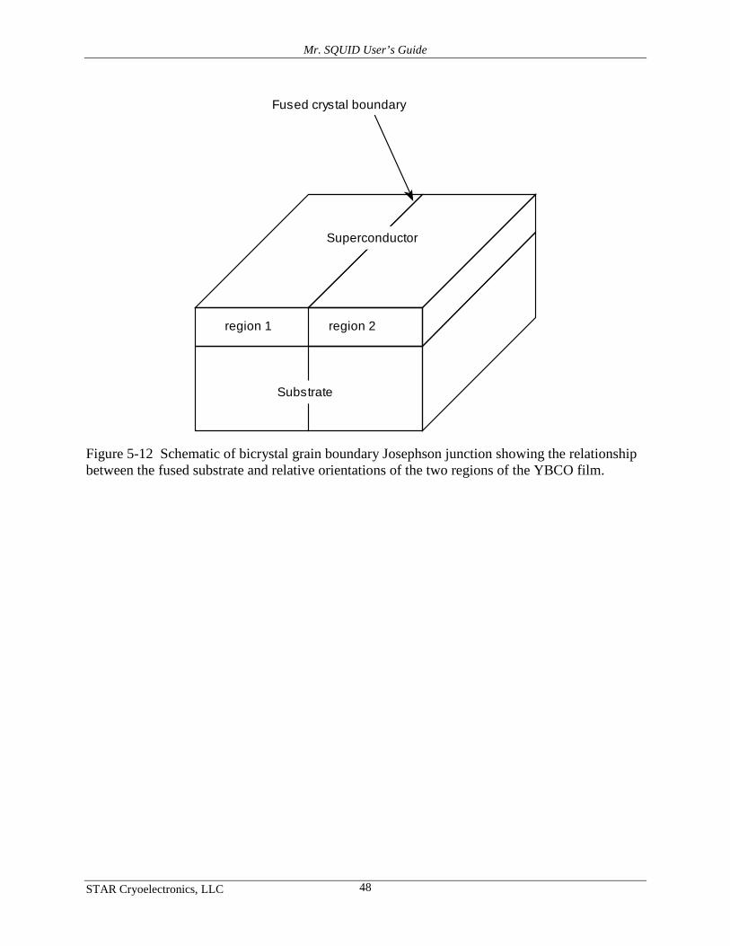
Mr. SQUID User’s Guide
STAR Cryoelectronics, LLC 48
Fused crystal boundary
Substrate
Superconductor
region 1 region 2
Figure 5-12 Schematic of bicrystal grain boundary Josephson junction showing the relationship between the fused substrate and relative orientations of the two regions of the YBCO film.
Mr. SQUID User’s Guide
STAR Cryoelectronics, LLC 49
6 TROUBLESHOOTING AND GETTING HELP
Mr. SQUID® has been designed to be a trouble-free, easy to operate system for the study of the physics and applications of SQUIDs. It is, however, a complex instrument incorporating sensitive Josephson junction electronics and cryogenic packaging. The SQUID probe itself undergoes tremendous thermal stresses during its repeated cycling between room temperature and liquid nitrogen. The cryogenic packaging system has been designed with two goals in mind: durability and visibility. These goals are not necessarily complementary, but we considered it important from an educational standpoint that the user be able to see the actual SQUID chip. With this in mind, there is the possibility that problems that you have encountered with Mr. SQUID® may be associated with a thermally induced failure in the probe. If this is the case, STAR Cryoelectronics will replace the defective probe at no cost for a period of one year from the purchase of the Mr. SQUID® system.
On the other hand, it is possible that the troubles you are encountering are of a less catastrophic nature and can be remedied by corrective actions outlined in this section. In the following table, we list some common difficulties along with recommended actions.

Mr. SQUID User’s Guide
STAR Cryoelectronics, LLC 50
6.1 Problems in V-I Mode
Output signal is: Action:
Point on scope is stationary regardless of settings
1. Check that the AC power supply is connected to the Mr. XSQUID box and plugged into the power mains, and that the POWER switch is in the ON position.
2. Check continuity and connections of the BNC cables to the oscilloscope.
3. Check scale settings on the oscilloscope.
Horizontal line regardless of settings
1. Check that the vertical input on the oscilloscope is configured for DC coupling.
2. Check the scale settings on the oscilloscope.
2. Check continuity and connection of VOLTAGE output BNC cable to oscilloscope.
Vertical line regardless of setting
1. Check that the vertical input on the oscilloscope is configured for DC coupling.
2. Check the scale settings on the oscilloscope.
2. Check the continuity and connection CURRENT BNC cable to oscilloscope.
3. Check the liquid nitrogen level.
Erratic or open-loop scope trace
1. Check that both oscilloscope inputs are DC coupled.
2. Check continuity and connection of both BNC cables to oscilloscope.
V-I curve has slight hysteresis
1. Check that both oscilloscope inputs are DC coupled.
2. If the oscilloscope has adjustable filters, increase the bandwidth.
3. Decrease the SWEEP OUTPUT control on the Mr. SQUID® box.

Mr. SQUID User’s Guide
STAR Cryoelectronics, LLC 51
V-I curve is linear
1. Check the continuity and connections of both BNC cables to the oscilloscope.
2. If the slope of the V-I curve is less than 10 Ω, see Sec. 6.3 on flux trapping and Sec. 6.5 on rf interference.
3. If the slope of the V-I curve is less than 10 Ω, try rotating and moving the dewar.
4. If slope of V-I curve is greater than about 10 Ω and less than a few hundred Ohms, check the liquid nitrogen level.
6.2 Problems in V-Φ Mode (Assuming Everything Works in V-I Mode)
Output signal is: Action:
Horizontal line
1. Check the scale settings on the oscilloscope.
2. Check that the vertical input on the oscilloscope is AC coupled.
3. Check for magnetized shield (see Sec. 6.4).
4. Check for RF interference.
V-Φ curve has slight hysteresis
1. Check that the horizontal input on the oscilloscope is DC coupled.
2. If the oscilloscope has adjustable filters, increase the bandwidth.
3. Decrease the SWEEP OUTPUT control on the Mr. SQUID® box.
6.3 Magnetic Flux Trapping in SQUIDs By far the most common difficulty encountered with Mr. SQUID® (and, for that matter, with all Josephson electronic circuits) is the effect of magnetic flux being trapped in the SQUID loop or in the junctions themselves. Trapped flux can greatly diminish the critical currents of the junctions. In the extreme (but, unfortunately, quite likely) case, the critical current in the SQUID may vanish entirely resulting in a linear V-I curve.
The cause of this problem is the extraordinary sensitivity of the SQUID and of Josephson junctions to applied magnetic fields. There are many sources of external magnetic fields in the
Mr. SQUID User’s Guide
STAR Cryoelectronics, LLC 52
operating environment of Mr. SQUID®. The most obvious one is the field of the Earth itself, which is approximately 0.5 Gauss in magnitude. If this entire field found its way into the SQUID, it would correspond to several hundred flux quanta in the loop. In addition, electrical devices of all sorts emanate magnetic fields that can affect Mr. SQUID®. It is for this reason that the end of the Mr. SQUID® probe that includes the chip is enclosed in a mu-metal shield. If this shielding were perfect, then external fields would not affect the SQUID at all. Bringing a small magnet close to the Mr. SQUID® dewar while the SQUID is operating should convince you that the shielding is not perfect.
In any event, it is important to cool down the SQUID into the superconducting state with the least amount of magnetic field present. Nearby computers can often cause trouble if they are on. In addition, it takes some time for the SQUID to reach liquid nitrogen temperature. Make sure you have waited long enough (perhaps a couple of minutes) before increasing the SWEEP OUTPUT.
If, after taking these precautions, the critical current is still miniscule or non-existent, warm up the probe again (it only needs to go above the critical temperature of the YBCO at 90 K) and cool it back down, perhaps rotating it to alter its orientation with respect to any local fields.
If, after several cooldowns, the V-I curve still shows a superconducting transition (i.e. the slope of the V-I curve indicates several hundred Ohms and suddenly switches to a few Ohms) but no supercurrent, one last thing to check is whether the black magnetic shield has itself become magnetized. Remember, the 0.5 Gauss field of the Earth forced through the SQUID will result in over a hundred trapped flux quanta, so even residual magnetizing of the shield at levels too small to measure by normal means can strongly affect the SQUID. This can happen if the shield has been dented, has been in extended contact with magnetized tools such as screwdrivers, has been rubbed by a magnet, or even has been rubbed by ordinary steel or iron. It is also possible for the shield to become magnetized during shipping, since many shipping companies will screen packages using x-ray machines, and these machines often generate magnetic fields. There is no easy way to tell if the mu-metal shield has become partly magnetized.
6.4 Degaussing the Magnetic Shield If you suspect that your Mr. SQUID® magnetic shield may be partly magnetized, there are products available that can be used to demagnetize the shield. This procedure is also called “degaussing.” We suggest that you use a bulk tape eraser typically used to erase video tapes, preferably one with an on-off switch, or a degaussing coil (diameter must be large enough so the Mr. SQUID® mu-metal shield will fit inside). Please read and follow both the Safety Instructions and the Operating Instructions that come with the bulk tape eraser or degaussing coil. To degauss a Mr. SQUID® mu-metal shield, one should follow the instructions that come with the tape eraser; in this case, the mu-metal shield is degaussed rather than recording tape. The instructions for degaussing the Mr. SQUID® magnetic shield are as follows:
STEP 1:
Remove the mu-metal shield from the Mr. SQUID® probe by loosening the setscrew at the top of the shield. Be sure the probe is at room temperature.
STEP 2:
Plug in and turn on the bulk tape eraser.
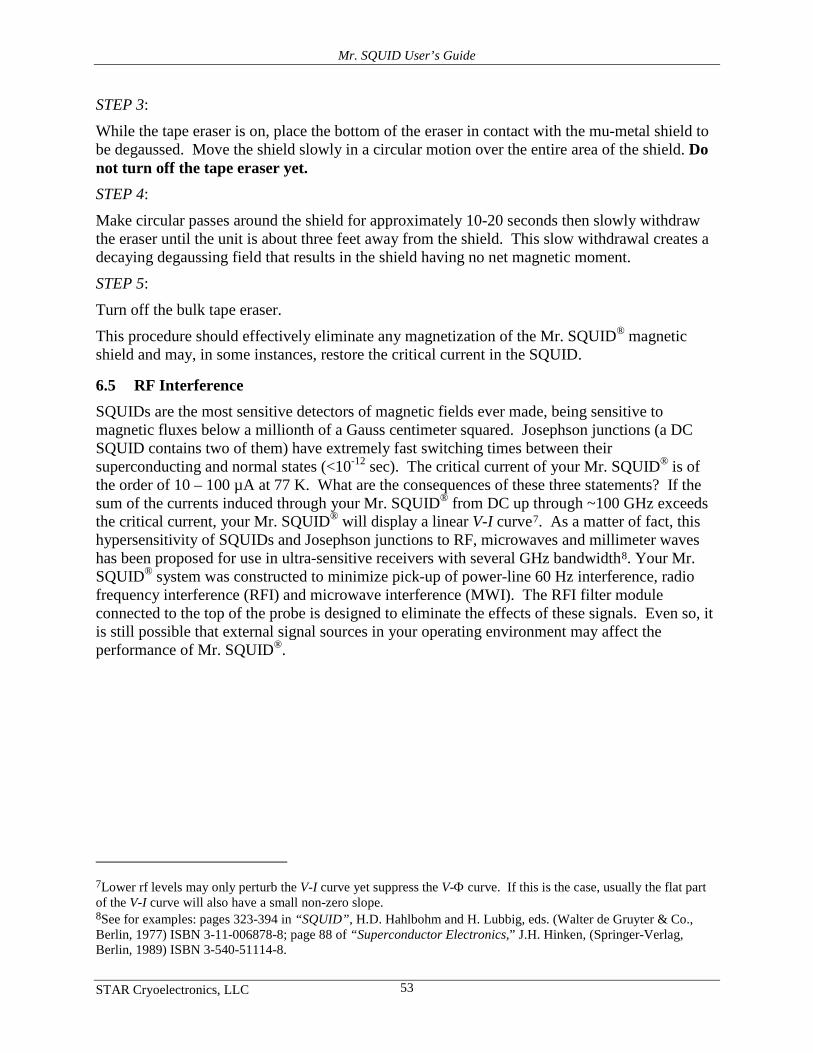
Mr. SQUID User’s Guide
STAR Cryoelectronics, LLC 53
STEP 3:
While the tape eraser is on, place the bottom of the eraser in contact with the mu-metal shield to be degaussed. Move the shield slowly in a circular motion over the entire area of the shield. Do not turn off the tape eraser yet. STEP 4:
Make circular passes around the shield for approximately 10-20 seconds then slowly withdraw the eraser until the unit is about three feet away from the shield. This slow withdrawal creates a decaying degaussing field that results in the shield having no net magnetic moment.
STEP 5:
Turn off the bulk tape eraser.
This procedure should effectively eliminate any magnetization of the Mr. SQUID® magnetic shield and may, in some instances, restore the critical current in the SQUID.
6.5 RF Interference SQUIDs are the most sensitive detectors of magnetic fields ever made, being sensitive to magnetic fluxes below a millionth of a Gauss centimeter squared. Josephson junctions (a DC SQUID contains two of them) have extremely fast switching times between their superconducting and normal states (<10-12 sec). The critical current of your Mr. SQUID® is of the order of 10 – 100 µA at 77 K. What are the consequences of these three statements? If the sum of the currents induced through your Mr. SQUID® from DC up through ~100 GHz exceeds the critical current, your Mr. SQUID® will display a linear V-I curve7. As a matter of fact, this hypersensitivity of SQUIDs and Josephson junctions to RF, microwaves and millimeter waves has been proposed for use in ultra-sensitive receivers with several GHz bandwidth8
. Your Mr. SQUID® system was constructed to minimize pick-up of power-line 60 Hz interference, radio frequency interference (RFI) and microwave interference (MWI). The RFI filter module connected to the top of the probe is designed to eliminate the effects of these signals. Even so, it is still possible that external signal sources in your operating environment may affect the performance of Mr. SQUID®.
7Lower rf levels may only perturb the V-I curve yet suppress the V-Φ curve. If this is the case, usually the flat part of the V-I curve will also have a small non-zero slope. 8See for examples: pages 323-394 in “SQUID”, H.D. Hahlbohm and H. Lubbig, eds. (Walter de Gruyter & Co., Berlin, 1977) ISBN 3-11-006878-8; page 88 of “Superconductor Electronics,” J.H. Hinken, (Springer-Verlag, Berlin, 1989) ISBN 3-540-51114-8.
Mr. SQUID User’s Guide
STAR Cryoelectronics, LLC 54
Above are V-I traces for a Mr. SQUID® in the absence and in the presence of RF interference of about 30 MHz. The critical current is totally suppressed when the RFI is present. The RFI was produced simply by pushing the “talk” button on a cordless telephone9
Other sources of RFI that are commonly encountered are computers, microwave ovens, garage door openers, pagers,
located a distance of about 1 foot from an operating Mr. SQUID® with the RFI filter module removed from the top of the probe.
10 CB radios, campus police radios, radio stations,11
A considerable amount of laboratory equipment also emits RF interference. Almost any high-voltage equipment, thin-film deposition equipment such as sputtering and e-beam evaporators, or electric welding equipment will also generate RFI. Electric motors that run fans or other equipment, particularly large electric motors, also generate considerable RFI. Any kind of rf or microwave test equipment will not only generate RFI, but many, for increased stability, keep their internal oscillators generating rf power even when their front panel power switches are in the “off” position.
and TV stations. These latter sources can be a problem at considerable distances, since most commercial stations broadcast hundreds of thousands of watts of RF power.
Unfortunately, the only way to definitively determine if RFI is causing problems for your Mr. SQUID® is to operate the Mr. SQUID® in an environment known to be RFI clean. Many low-temperature physics laboratories have RF shielded rooms as do many electrical engineering departments. However, if you do not have access to an RF shielded room, the first thing to do is to determine if any RF sources are nearby. When looking for possible sources of RFI, try to cover everything within 50 meters or so. Walls, even brick and concrete, will often not attenuate RFI very much. Remember to not only look in the surrounding area, but also on several floors above and below the room in which you are attempting to run your Mr. SQUID®.
9SONY model SPP-50. 10Paging systems in buildings often distribute their broadcasts by injecting their rf carrier into the building power lines. This rf can interfere with the operation of your Mr. SQUID. 11Campus radio stations often distribute their broadcasts by injecting their rf carrier into the campus power lines to avoid certain FCC restrictions. This rf can interfere with the operation of your Mr. SQUID®.

Mr. SQUID User’s Guide
STAR Cryoelectronics, LLC 55
After you have identified possible RFI sources, you should try switching them off, one by one, while watching the V-I or V-Φ curve of your Mr. SQUID®. This will allow you to identify which of the possible sources are causing the largest problems. Basically, just keep turning things off until the RFI goes away.
Some sources of RFI either cannot be turned off or are not under your control. In this case, you will need to consider operating your Mr. SQUID® at another location. For example, if there are TV or radio broadcast towers nearby, try operating your Mr. SQUID® in a room such that the bulk of the building is between your Mr. SQUID® and the broadcast tower. Another solution is to place the Mr. SQUID® system in a closed metal box (a “Faraday cage”) to screen out the RFI.
In the past, SQUID systems were primarily operated in controlled environments in which detrimental external influences such as RFI were carefully kept away. Mr. SQUID® is a system designed to be used in ordinary undergraduate laboratories. However, it is still a SQUID, which is an extraordinarily sensitive detector of electromagnetic signals. For this reason, there are some locations in which it simply will never work properly without measures such as the Faraday cage mentioned above. Your particular laboratory could possibly be such a location, in the final analysis. For this reason, before you become convinced that there is an internal problem with your Mr. SQUID®, make sure you operate it in a variety of locations.
What if it never looks right? All Mr. SQUID® probes have been tested at STAR Cryoelectronics in unshielded laboratory space and have demonstrated acceptable characteristics. It is possible that something may have gone wrong with the SQUID subsequent to its departure from our test lab, but a chip or probe failure is unlikely to result in a linear V-I curve of the sort usually associated with flux trapping (i.e., displaying a superconducting transition below which the SQUID V-I curve has a resistance of a few Ohms). Real chip failures generally yield a more catastrophic outcome. If all else fails, call us and describe your problem.
6.6 Customer Service We are anxious to help you make the most of your Mr. SQUID® system. You can best communicate with us by email at [email protected]
When you do contact us, please send a description of the problem, the serial number of your probe and electronics box, and descriptions of your V-I and V-Φ curves (values of Ic, RN and ∆V). You can also reach us weekdays between 8:00 a.m. and 6:00 p.m. Mountain Time at (505) 424-6454, or by fax at (505) 424-8225.

Mr. SQUID User’s Guide
STAR Cryoelectronics, LLC 56
7 ADVANCED EXPERIMENTS
This section of the User's Guide details a series of more advanced experiments using Mr. SQUID® that go beyond the basic functions of the SQUID system. Unlike the basic functions, these experiments require various additional pieces of equipment and in some cases assembly of simple electronic circuits. Where possible, the circuits used in the experiments can be built from readily available electronic components that can be obtained from most electronic parts suppliers.
The effort and experimental skills required to perform these experiments goes beyond the level of the basic operation of the system, but they are well within the scope of an advanced undergraduate laboratory course. The intent of these experiments is to demonstrate the operation and applications of SQUIDs and superconductivity, not to teach solid-state electronics. Some of the experiments can be performed during the course of a single laboratory session, while others may take more time.
We enthusiastically welcome feedback from users and particularly look forward to suggestions and descriptions for new experiments for the Mr. SQUID® system as well as improvements to the present experiments. We would like to include them in later versions of the User's Guide and in supplements for current users. Thank you in advance for your help.

Mr. SQUID User’s Guide
STAR Cryoelectronics, LLC 57
7.1 Resistance vs. Temperature of the YBCO SQUID Purpose This experiment will allow you to observe the superconducting transition of the YBCO film that forms the SQUID in Mr. SQUID®. By tracking the resistance of the SQUID with the V-I curve, you can watch the YBCO undergo its superconducting transition. The additional equipment needed for this experiment allows you to measure the temperature of the SQUID chip as it is cooled down to liquid nitrogen temperature. Equipment For this experiment you will need:
• A glass encapsulated silicon diode (e.g., 1N914 or equivalent),
• 200 cm of insulated copper magnet wire of size 32 to 40 AWG12
• A digital volt meter (DVM) with sub-millivolt resolution,
(this corresponds to a diameter of 0.020 to 0.008 mm),
13
• A soldering iron and electronics-grade solder,
• A binder clip (available from any stationary supplier),
• One or two cotton balls,
• Masking tape,
• An active DC constant current source capable of supplying 10 µA of current with a voltage compliance of at least 2 volts.
If you do not have a constant current source then you will also need:
• A general-purpose operational amplifier (e.g., LM741N),
• A zener diode in the range of 2.5 to 7 volts (e.g., 1N4733A),
• A selection of ¼ Watt resistors in the range of 1 kΩ through 100 kΩ,
• A capacitor in the range of 100 pF to 100 nF,
• A 9-Volt battery,
• A solderless breadboard.14
In this experiment, we will use a common silicon diode to measure the temperature of the SQUID in the Mr. SQUID® probe. Silicon diodes are a common and accurate way to measure temperature from 300 K down to liquid helium temperatures (4.2 K). They are simple to use, 12Such as Belden Beldsol Solderable Magnet Wire Types 8081 through 8087. 13Such as a Kiethley Model 197 or Agilent 34401A digital voltmeter. Millivolt resolution may be acceptable but will limit the accuracy of the temperature measurements. 14Such as 3M Electronic Specialty part number 922306.
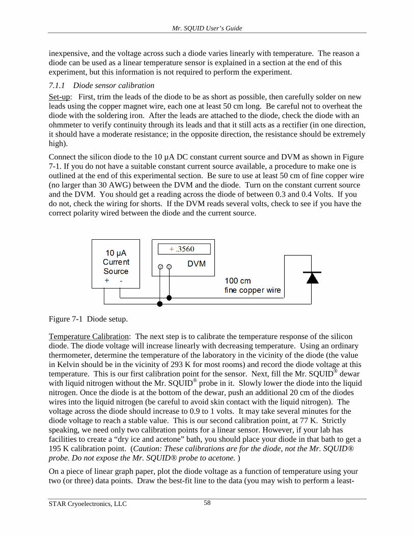
Mr. SQUID User’s Guide
STAR Cryoelectronics, LLC 58
inexpensive, and the voltage across such a diode varies linearly with temperature. The reason a diode can be used as a linear temperature sensor is explained in a section at the end of this experiment, but this information is not required to perform the experiment.
7.1.1 Diode sensor calibration Set-up: First, trim the leads of the diode to be as short as possible, then carefully solder on new leads using the copper magnet wire, each one at least 50 cm long. Be careful not to overheat the diode with the soldering iron. After the leads are attached to the diode, check the diode with an ohmmeter to verify continuity through its leads and that it still acts as a rectifier (in one direction, it should have a moderate resistance; in the opposite direction, the resistance should be extremely high).
Connect the silicon diode to the 10 µA DC constant current source and DVM as shown in Figure 7-1. If you do not have a suitable constant current source available, a procedure to make one is outlined at the end of this experimental section. Be sure to use at least 50 cm of fine copper wire (no larger than 30 AWG) between the DVM and the diode. Turn on the constant current source and the DVM. You should get a reading across the diode of between 0.3 and 0.4 Volts. If you do not, check the wiring for shorts. If the DVM reads several volts, check to see if you have the correct polarity wired between the diode and the current source.
Figure 7-1 Diode setup.
Temperature Calibration: The next step is to calibrate the temperature response of the silicon diode. The diode voltage will increase linearly with decreasing temperature. Using an ordinary thermometer, determine the temperature of the laboratory in the vicinity of the diode (the value in Kelvin should be in the vicinity of 293 K for most rooms) and record the diode voltage at this temperature. This is our first calibration point for the sensor. Next, fill the Mr. SQUID® dewar with liquid nitrogen without the Mr. SQUID® probe in it. Slowly lower the diode into the liquid nitrogen. Once the diode is at the bottom of the dewar, push an additional 20 cm of the diodes wires into the liquid nitrogen (be careful to avoid skin contact with the liquid nitrogen). The voltage across the diode should increase to 0.9 to 1 volts. It may take several minutes for the diode voltage to reach a stable value. This is our second calibration point, at 77 K. Strictly speaking, we need only two calibration points for a linear sensor. However, if your lab has facilities to create a “dry ice and acetone” bath, you should place your diode in that bath to get a 195 K calibration point. (Caution: These calibrations are for the diode, not the Mr. SQUID® probe. Do not expose the Mr. SQUID® probe to acetone. ) On a piece of linear graph paper, plot the diode voltage as a function of temperature using your two (or three) data points. Draw the best-fit line to the data (you may wish to perform a least-
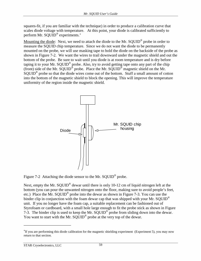
Mr. SQUID User’s Guide
STAR Cryoelectronics, LLC 59
squares-fit, if you are familiar with the technique) in order to produce a calibration curve that scales diode voltage with temperature. At this point, your diode is calibrated sufficiently to perform Mr. SQUID® experiments.*
Mounting the diode: Next, we need to attach the diode to the Mr. SQUID® probe in order to measure the SQUID chip temperature. Since we do not want the diode to be permanently mounted on the probe, we will use masking tape to hold the diode on the backside of the probe as shown in
Figure 7-2. We want the wires to trail downward under the magnetic shield and out the bottom of the probe. Be sure to wait until you diode is at room temperature and is dry before taping it to your Mr. SQUID® probe. Also, try to avoid getting tape onto any part of the chip (front) side of the Mr. SQUID® probe. Place the Mr. SQUID® magnetic shield on the Mr. SQUID® probe so that the diode wires come out of the bottom. Stuff a small amount of cotton into the bottom of the magnetic shield to block the opening. This will improve the temperature uniformity of the region inside the magnetic shield.
Mr. SQUID chip housing Diode
Figure 7-2 Attaching the diode sensor to the Mr. SQUID® probe.
Next, empty the Mr. SQUID® dewar until there is only 10-12 cm of liquid nitrogen left at the bottom (you can pour the unwanted nitrogen onto the floor, making sure to avoid people’s feet, etc.) Place the Mr. SQUID® probe into the dewar as shown in Figure 7-3. You can use the binder clip in conjunction with the foam dewar cap that was shipped with your Mr. SQUID® unit. If you no longer have the foam cap, a suitable replacement can be fashioned out of Styrofoam or cardboard, with a small hole large enough to fit the probe stick as shown in Figure 7-3. The binder clip is used to keep the Mr. SQUID® probe from sliding down into the dewar. You want to start with the Mr. SQUID® probe at the very top of the dewar.
*If you are performing this diode calibration for the magnetic shielding experiment (Experiment 5), you may now return to that section.
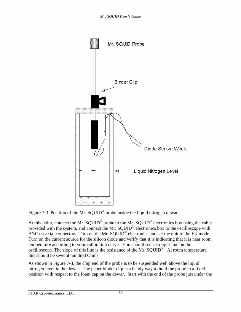
Mr. SQUID User’s Guide
STAR Cryoelectronics, LLC 60
Figure 7-3 Position of the Mr. SQUID® probe inside the liquid nitrogen dewar.
At this point, connect the Mr. SQUID® probe to the Mr. SQUID® electronics box using the cable provided with the system, and connect the Mr. SQUID® electronics box to the oscilloscope with BNC co-axial connectors. Turn on the Mr. SQUID® electronics and set the unit to the V-I mode. Turn on the current source for the silicon diode and verify that it is indicating that it is near room temperature according to your calibration curve. You should see a straight line on the oscilloscope. The slope of this line is the resistance of the Mr. SQUID®. At room temperature this should be several hundred Ohms.
As shown in Figure 7-3, the chip end of the probe is to be suspended well above the liquid nitrogen level in the dewar. The paper binder clip is a handy way to hold the probe in a fixed position with respect to the foam cap on the dewar. Start with the end of the probe just under the
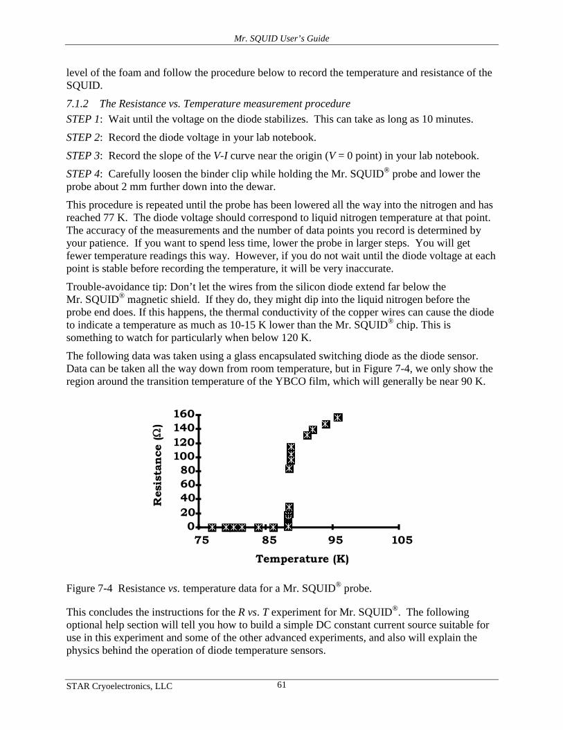
Mr. SQUID User’s Guide
STAR Cryoelectronics, LLC 61
level of the foam and follow the procedure below to record the temperature and resistance of the SQUID.
7.1.2 The Resistance vs. Temperature measurement procedure STEP 1: Wait until the voltage on the diode stabilizes. This can take as long as 10 minutes.
STEP 2: Record the diode voltage in your lab notebook.
STEP 3: Record the slope of the V-I curve near the origin (V = 0 point) in your lab notebook.
STEP 4: Carefully loosen the binder clip while holding the Mr. SQUID® probe and lower the probe about 2 mm further down into the dewar.
This procedure is repeated until the probe has been lowered all the way into the nitrogen and has reached 77 K. The diode voltage should correspond to liquid nitrogen temperature at that point. The accuracy of the measurements and the number of data points you record is determined by your patience. If you want to spend less time, lower the probe in larger steps. You will get fewer temperature readings this way. However, if you do not wait until the diode voltage at each point is stable before recording the temperature, it will be very inaccurate.
Trouble-avoidance tip: Don’t let the wires from the silicon diode extend far below the Mr. SQUID® magnetic shield. If they do, they might dip into the liquid nitrogen before the probe end does. If this happens, the thermal conductivity of the copper wires can cause the diode to indicate a temperature as much as 10-15 K lower than the Mr. SQUID® chip. This is something to watch for particularly when below 120 K.
The following data was taken using a glass encapsulated switching diode as the diode sensor. Data can be taken all the way down from room temperature, but in Figure 7-4, we only show the region around the transition temperature of the YBCO film, which will generally be near 90 K.
Temperature (K)
Res
ista
nce
(Ω)
0 20 40 60 80
100 120 140 160
75 85 95 105
Figure 7-4 Resistance vs. temperature data for a Mr. SQUID® probe.
This concludes the instructions for the R vs. T experiment for Mr. SQUID®. The following optional help section will tell you how to build a simple DC constant current source suitable for use in this experiment and some of the other advanced experiments, and also will explain the physics behind the operation of diode temperature sensors.
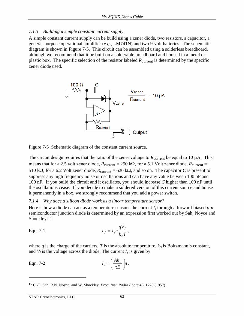
Mr. SQUID User’s Guide
STAR Cryoelectronics, LLC 62
7.1.3 Building a simple constant current supply A simple constant current supply can be build using a zener diode, two resistors, a capacitor, a general-purpose operational amplifier (e.g., LM741N) and two 9-volt batteries. The schematic diagram is shown in Figure 7-5. This circuit can be assembled using a solderless breadboard, although we recommend that it be built on a solderable breadboard and housed in a metal or plastic box. The specific selection of the resistor labeled Rcurrent is determined by the specific zener diode used.
Figure 7-5 Schematic diagram of the constant current source.
The circuit design requires that the ratio of the zener voltage to Rcurrent be equal to 10 µA. This means that for a 2.5 volt zener diode, Rcurrent = 250 kΩ, for a 5.1 Volt zener diode, Rcurrent = 510 kΩ, for a 6.2 Volt zener diode, Rcurrent = 620 kΩ, and so on. The capacitor C is present to suppress any high frequency noise or oscillations and can have any value between 100 pF and 100 nF. If you build the circuit and it oscillates, you should increase C higher than 100 nF until the oscillations cease. If you decide to make a soldered version of this current source and house it permanently in a box, we strongly recommend that you add a power switch.
7.1.4 Why does a silicon diode work as a linear temperature sensor? Here is how a diode can act as a temperature sensor: the current Is through a forward-biased p-n semiconductor junction diode is determined by an expression first worked out by Sah, Noyce and Shockley:15
Eqn. 7-1
TkqV
eIIB
fsf = ,
where q is the charge of the carriers, T is the absolute temperature, kB is Boltzmann’s constant, and Vf is the voltage across the diode. The current Is is given by:
Eqn. 7-2 nE
AkI Bs
τ= ,
15 C.-T. Sah, R.N. Noyce, and W. Shockley, Proc. Inst. Radio Engrs 45, 1228 (1957).
Mr. SQUID User’s Guide
STAR Cryoelectronics, LLC 63
where A is the p-n junction area, τ is the average carrier lifetime, E is the electric field in the depletion region of the p-n junction, and n is the carrier density. The value of n is given by
Eqn. 7-3
−
π≈
µ−−
π=
TkETmk
TkETmkn
B
gB
B
cB
2exp2
41)(
exp241 2/3
2
2/3
2
where Ec is the conduction band energy, Eg is the intrinsic energy gap in the semiconductor, µ is the carrier chemical potential, and m is the effective mass of the carriers. Combining these three equations and solving for Vf as a function of T, and assuming we have a fixed forward bias current (If) through the diode, we find:
Eqn. 7-4 q
TkITq
ETV B
fg
f2)ln()ln(
25)ln()(
−+α−= ,
where
Eqn. 7-5
τ
π=α
EAkTmk BB
2/3
2
241
.
Note that the above equation for Vf(T) says that a p-n semiconductor junction, under constant forward bias current (fixed If ), will display a voltage that will be approximately linear with temperature and will depend only on the intrinsic gap of the semiconductor, independent of the specific doping. It also says that if one plots Vf(T) vs. T, one can take the high-temperature region (before the (5/2)ln(T) term becomes significant) and use it to extrapolate Vf to T = 0. The zero intercept will give one the value of the semiconductor band gap, Eg. In other words, all diodes made from a specific semiconductor (such as silicon) should display the same approximately linear behavior as a function of temperature under the same constant current conditions. As a practical matter, the above explanation breaks down at temperatures below about 30 K for silicon diodes. Below that temperature, a different mechanism takes over the diode behavior, which still results in a linear Vf(T) down to almost 1 K, but with a different slope. Internal stresses in the silicon diode chip can also cause nonlinear Vf(T) relationships, and so diodes sold specifically as cryogenic sensors are mounted in special packages to minimize the stresses from thermal contraction.
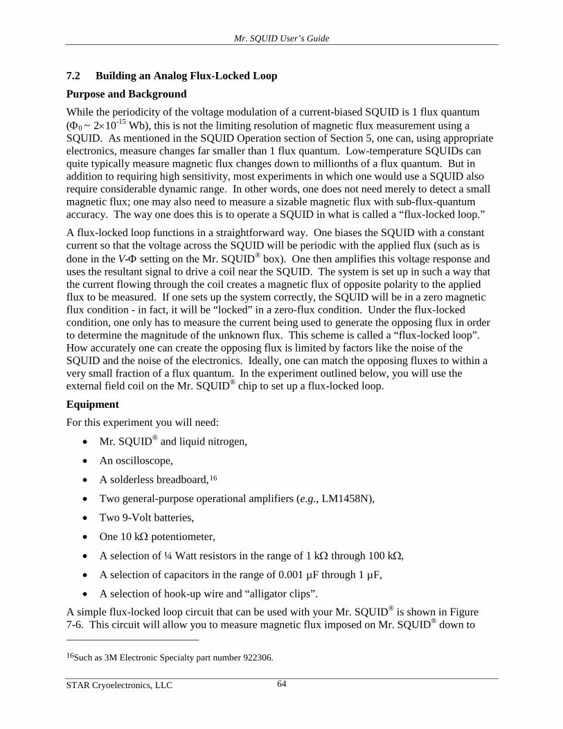
Mr. SQUID User’s Guide
STAR Cryoelectronics, LLC 64
7.2 Building an Analog Flux-Locked Loop Purpose and Background While the periodicity of the voltage modulation of a current-biased SQUID is 1 flux quantum (Φ0 ~ 2×10-15 Wb), this is not the limiting resolution of magnetic flux measurement using a SQUID. As mentioned in the SQUID Operation section of Section 5, one can, using appropriate electronics, measure changes far smaller than 1 flux quantum. Low-temperature SQUIDs can quite typically measure magnetic flux changes down to millionths of a flux quantum. But in addition to requiring high sensitivity, most experiments in which one would use a SQUID also require considerable dynamic range. In other words, one does not need merely to detect a small magnetic flux; one may also need to measure a sizable magnetic flux with sub-flux-quantum accuracy. The way one does this is to operate a SQUID in what is called a “flux-locked loop.”
A flux-locked loop functions in a straightforward way. One biases the SQUID with a constant current so that the voltage across the SQUID will be periodic with the applied flux (such as is done in the V-Φ setting on the Mr. SQUID® box). One then amplifies this voltage response and uses the resultant signal to drive a coil near the SQUID. The system is set up in such a way that the current flowing through the coil creates a magnetic flux of opposite polarity to the applied flux to be measured. If one sets up the system correctly, the SQUID will be in a zero magnetic flux condition - in fact, it will be “locked” in a zero-flux condition. Under the flux-locked condition, one only has to measure the current being used to generate the opposing flux in order to determine the magnitude of the unknown flux. This scheme is called a “flux-locked loop”. How accurately one can create the opposing flux is limited by factors like the noise of the SQUID and the noise of the electronics. Ideally, one can match the opposing fluxes to within a very small fraction of a flux quantum. In the experiment outlined below, you will use the external field coil on the Mr. SQUID® chip to set up a flux-locked loop.
Equipment For this experiment you will need:
• Mr. SQUID® and liquid nitrogen,
• An oscilloscope,
• A solderless breadboard,16
• Two general-purpose operational amplifiers (e.g., LM1458N),
• Two 9-Volt batteries,
• One 10 kΩ potentiometer,
• A selection of ¼ Watt resistors in the range of 1 kΩ through 100 kΩ,
• A selection of capacitors in the range of 0.001 µF through 1 µF,
• A selection of hook-up wire and “alligator clips”.
A simple flux-locked loop circuit that can be used with your Mr. SQUID® is shown in Figure 7-6. This circuit will allow you to measure magnetic flux imposed on Mr. SQUID® down to 16Such as 3M Electronic Specialty part number 922306.
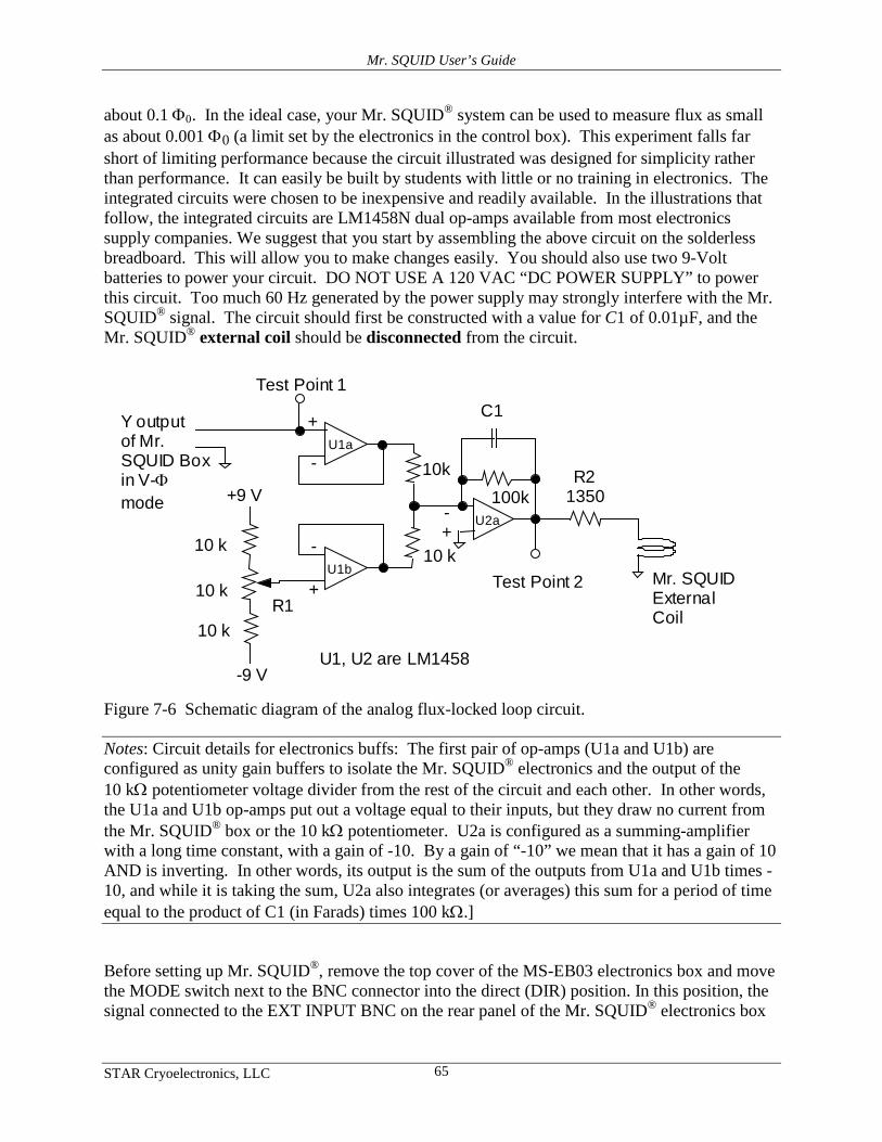
Mr. SQUID User’s Guide
STAR Cryoelectronics, LLC 65
about 0.1 Φ0. In the ideal case, your Mr. SQUID® system can be used to measure flux as small as about 0.001 Φ0 (a limit set by the electronics in the control box). This experiment falls far short of limiting performance because the circuit illustrated was designed for simplicity rather than performance. It can easily be built by students with little or no training in electronics. The integrated circuits were chosen to be inexpensive and readily available. In the illustrations that follow, the integrated circuits are LM1458N dual op-amps available from most electronics supply companies. We suggest that you start by assembling the above circuit on the solderless breadboard. This will allow you to make changes easily. You should also use two 9-Volt batteries to power your circuit. DO NOT USE A 120 VAC “DC POWER SUPPLY” to power this circuit. Too much 60 Hz generated by the power supply may strongly interfere with the Mr. SQUID® signal. The circuit should first be constructed with a value for C1 of 0.01µF, and the Mr. SQUID® external coil should be disconnected from the circuit.
+
-
-
+
U1a
U1b
100k
10 k
10 k
10 k
- +
U2a
10k
10 k Test Point 2
+9 V
-9 V
1350
Test Point 1
Mr. SQUID External Coil
U1, U2 are LM1458
R1
C1
R2
Y output of Mr. SQUID Box in V-Φ mode
Figure 7-6 Schematic diagram of the analog flux-locked loop circuit.
Notes: Circuit details for electronics buffs: The first pair of op-amps (U1a and U1b) are configured as unity gain buffers to isolate the Mr. SQUID® electronics and the output of the 10 kΩ potentiometer voltage divider from the rest of the circuit and each other. In other words, the U1a and U1b op-amps put out a voltage equal to their inputs, but they draw no current from the Mr. SQUID® box or the 10 kΩ potentiometer. U2a is configured as a summing-amplifier with a long time constant, with a gain of -10. By a gain of “-10” we mean that it has a gain of 10 AND is inverting. In other words, its output is the sum of the outputs from U1a and U1b times -10, and while it is taking the sum, U2a also integrates (or averages) this sum for a period of time equal to the product of C1 (in Farads) times 100 kΩ.]
Before setting up Mr. SQUID®, remove the top cover of the MS-EB03 electronics box and move the MODE switch next to the BNC connector into the direct (DIR) position. In this position, the signal connected to the EXT INPUT BNC on the rear panel of the Mr. SQUID® electronics box
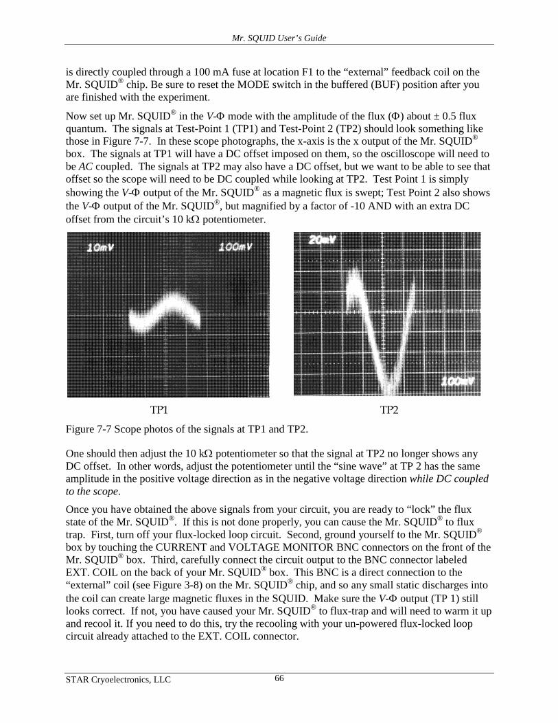
Mr. SQUID User’s Guide
STAR Cryoelectronics, LLC 66
is directly coupled through a 100 mA fuse at location F1 to the “external” feedback coil on the Mr. SQUID® chip. Be sure to reset the MODE switch in the buffered (BUF) position after you are finished with the experiment.
Now set up Mr. SQUID® in the V-Φ mode with the amplitude of the flux (Φ) about ± 0.5 flux quantum. The signals at Test-Point 1 (TP1) and Test-Point 2 (TP2) should look something like those in Figure 7-7. In these scope photographs, the x-axis is the x output of the Mr. SQUID® box. The signals at TP1 will have a DC offset imposed on them, so the oscilloscope will need to be AC coupled. The signals at TP2 may also have a DC offset, but we want to be able to see that offset so the scope will need to be DC coupled while looking at TP2. Test Point 1 is simply showing the V-Φ output of the Mr. SQUID® as a magnetic flux is swept; Test Point 2 also shows the V-Φ output of the Mr. SQUID®, but magnified by a factor of -10 AND with an extra DC offset from the circuit’s 10 kΩ potentiometer.
TP1 TP2 Figure 7-7 Scope photos of the signals at TP1 and TP2.
One should then adjust the 10 kΩ potentiometer so that the signal at TP2 no longer shows any DC offset. In other words, adjust the potentiometer until the “sine wave” at TP 2 has the same amplitude in the positive voltage direction as in the negative voltage direction while DC coupled to the scope.
Once you have obtained the above signals from your circuit, you are ready to “lock” the flux state of the Mr. SQUID®. If this is not done properly, you can cause the Mr. SQUID® to flux trap. First, turn off your flux-locked loop circuit. Second, ground yourself to the Mr. SQUID® box by touching the CURRENT and VOLTAGE MONITOR BNC connectors on the front of the Mr. SQUID® box. Third, carefully connect the circuit output to the BNC connector labeled EXT. COIL on the back of your Mr. SQUID® box. This BNC is a direct connection to the “external” coil (see Figure 3-8) on the Mr. SQUID® chip, and so any small static discharges into the coil can create large magnetic fluxes in the SQUID. Make sure the V-Φ output (TP 1) still looks correct. If not, you have caused your Mr. SQUID® to flux-trap and will need to warm it up and recool it. If you need to do this, try the recooling with your un-powered flux-locked loop circuit already attached to the EXT. COIL connector.
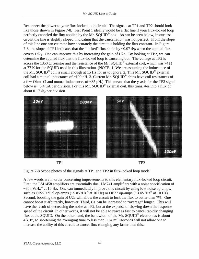
Mr. SQUID User’s Guide
STAR Cryoelectronics, LLC 67
Reconnect the power to your flux-locked loop circuit. The signals at TP1 and TP2 should look like those shown in Figure 7-8. Test Point 1 ideally would be a flat line if your flux-locked loop perfectly canceled the flux applied by the Mr. SQUID® box. As can be seen below, in our test circuit the line is slightly sloped, indicating that the cancellation was not perfect. From the slope of this line one can estimate how accurately the circuit is holding the flux constant. In Figure 7-8, the slope of TP1 indicates that the “locked” flux shifts by ~0.07 Φ0 when the applied flux covers 1 Φ0. One can improve this by increasing the gain of U2a. By looking at TP2, we can determine the applied flux that the flux-locked loop is canceling out. The voltage at TP2 is across the 1350 Ω resistor and the resistance of the Mr. SQUID® external coil, which was 74 Ω at 77 K for the SQUID used in this illustration. (NOTE: 1. We are assuming the inductance of the Mr. SQUID® coil is small enough at 15 Hz for us to ignore. 2. This Mr. SQUID® external coil had a mutual inductance of ~100 pH. 3. Current Mr. SQUID® chips have coil resistances of a few Ohms Ω and mutual inductances of ~35 pH.) This means that the y-axis for the TP2 signal below is ~3.4 µA per division. For this Mr. SQUID® external coil, this translates into a flux of about 0.17 Φ0 per division.
TP1 TP2
Figure 7-8 Scope photos of the signals at TP1 and TP2 in flux-locked loop mode.
A few words are in order concerning improvements to this elementary flux-locked loop circuit. First, the LM1458 amplifiers are essentially dual LM741 amplifiers with a noise specification of ~80 nV/Hz½ at 10 Hz. One can immediately improve this circuit by using low-noise op-amps, such as OP270 dual op-amps (~5 nV/Hz½ at 10 Hz) or OP27 op-amps (~3 nV/Hz½ at 10 Hz). Second, boosting the gain of U2a will allow the circuit to lock the flux to better than 7%. One cannot boost it arbitrarily, however. Third, C1 can be increased to “average” longer. This will have the result of decreasing the noise at TP2, but at the expense of slowing down the response speed of the circuit. In other words, it will not be able to react as fast to cancel rapidly changing flux at the SQUID. On the other hand, the bandwidth of the Mr. SQUID® electronics is about 4 kHz, so shortening the averaging time to less than ~0.4 milliseconds will not allow one to increase the ability of this circuit to cancel flux changing any faster than this.
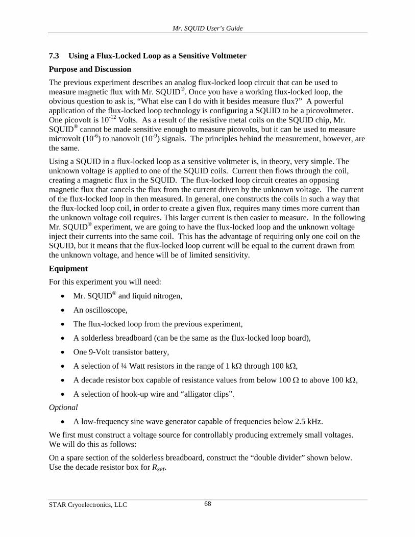
Mr. SQUID User’s Guide
STAR Cryoelectronics, LLC 68
7.3 Using a Flux-Locked Loop as a Sensitive Voltmeter Purpose and Discussion The previous experiment describes an analog flux-locked loop circuit that can be used to measure magnetic flux with Mr. SQUID®. Once you have a working flux-locked loop, the obvious question to ask is, “What else can I do with it besides measure flux?” A powerful application of the flux-locked loop technology is configuring a SQUID to be a picovoltmeter. One picovolt is 10-12 Volts. As a result of the resistive metal coils on the SQUID chip, Mr. SQUID® cannot be made sensitive enough to measure picovolts, but it can be used to measure microvolt (10-6) to nanovolt (10-9) signals. The principles behind the measurement, however, are the same.
Using a SQUID in a flux-locked loop as a sensitive voltmeter is, in theory, very simple. The unknown voltage is applied to one of the SQUID coils. Current then flows through the coil, creating a magnetic flux in the SQUID. The flux-locked loop circuit creates an opposing magnetic flux that cancels the flux from the current driven by the unknown voltage. The current of the flux-locked loop in then measured. In general, one constructs the coils in such a way that the flux-locked loop coil, in order to create a given flux, requires many times more current than the unknown voltage coil requires. This larger current is then easier to measure. In the following Mr. SQUID® experiment, we are going to have the flux-locked loop and the unknown voltage inject their currents into the same coil. This has the advantage of requiring only one coil on the SQUID, but it means that the flux-locked loop current will be equal to the current drawn from the unknown voltage, and hence will be of limited sensitivity.
Equipment For this experiment you will need:
• Mr. SQUID® and liquid nitrogen,
• An oscilloscope,
• The flux-locked loop from the previous experiment,
• A solderless breadboard (can be the same as the flux-locked loop board),
• One 9-Volt transistor battery,
• A selection of ¼ Watt resistors in the range of 1 kΩ through 100 kΩ,
• A decade resistor box capable of resistance values from below 100 Ω to above 100 kΩ,
• A selection of hook-up wire and “alligator clips”. Optional
• A low-frequency sine wave generator capable of frequencies below 2.5 kHz.
We first must construct a voltage source for controllably producing extremely small voltages. We will do this as follows:
On a spare section of the solderless breadboard, construct the “double divider” shown below. Use the decade resistor box for Rset.
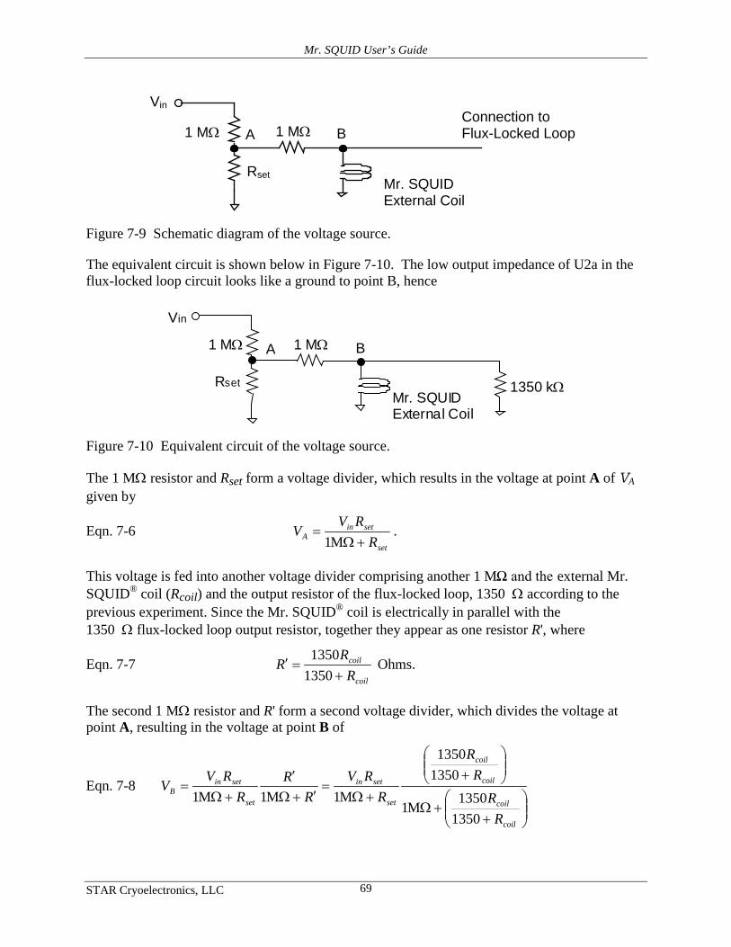
Mr. SQUID User’s Guide
STAR Cryoelectronics, LLC 69
Rset
1 MΩ
Mr. SQUID External Coil
1 MΩ
Vin Connection to Flux-Locked Loop A B
Figure 7-9 Schematic diagram of the voltage source.
The equivalent circuit is shown below in Figure 7-10. The low output impedance of U2a in the flux-locked loop circuit looks like a ground to point B, hence
1 MΩ
Mr. SQUID External Coil
Rset
1 MΩ
1350 kΩ
A B
Vin
Figure 7-10 Equivalent circuit of the voltage source.
The 1 MΩ resistor and Rset form a voltage divider, which results in the voltage at point A of VA given by
Eqn. 7-6 set
setinA R
RVV
+Ω=
M1.
This voltage is fed into another voltage divider comprising another 1 MΩ and the external Mr. SQUID® coil (Rcoil) and the output resistor of the flux-locked loop, 1350 Ω according to the previous experiment. Since the Mr. SQUID® coil is electrically in parallel with the 1350 Ω flux-locked loop output resistor, together they appear as one resistor R', where
Eqn. 7-7 coil
coil
RR
R+
=′13501350
Ohms.
The second 1 MΩ resistor and R' form a second voltage divider, which divides the voltage at point A, resulting in the voltage at point B of
Eqn. 7-8
+
+Ω
+
+Ω=
′+Ω′
+Ω=
coil
coil
coil
coil
set
setin
set
setinB
RR
RR
RRV
RR
RRV
V
13501350
M1
13501350
M1M1M1
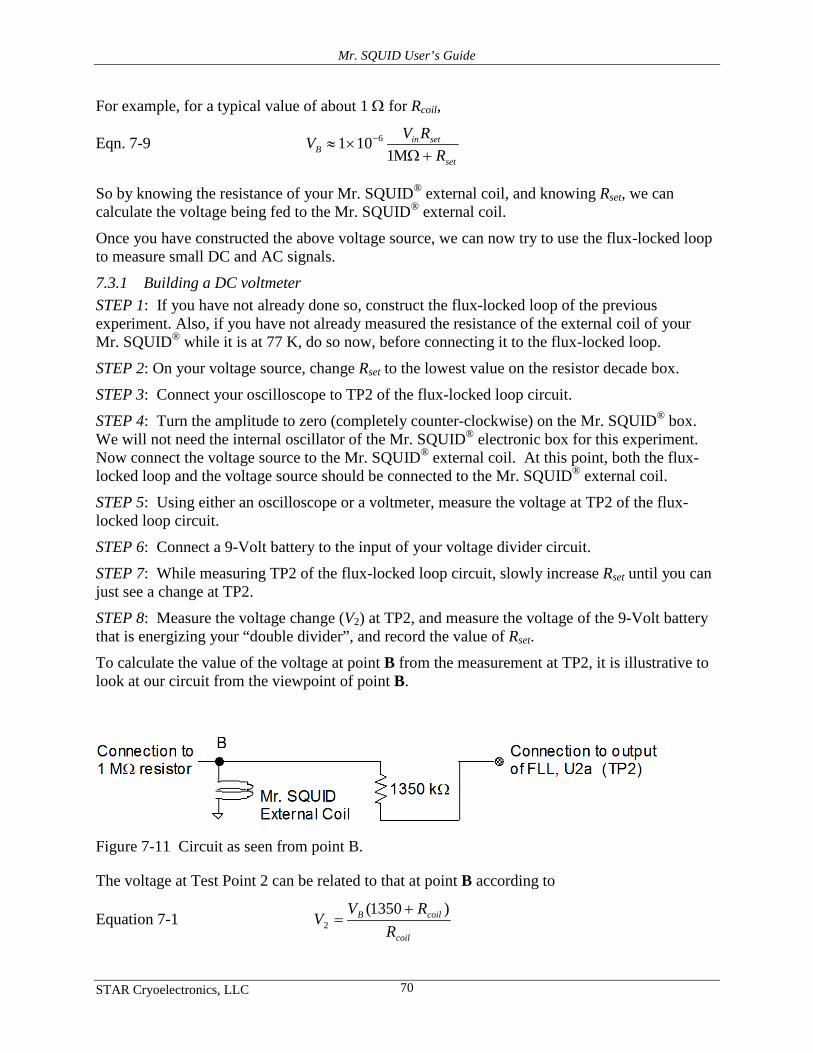
Mr. SQUID User’s Guide
STAR Cryoelectronics, LLC 70
For example, for a typical value of about 1 Ω for Rcoil,
Eqn. 7-9 set
setinB R
RVV+Ω
×≈ −
M1101 6
So by knowing the resistance of your Mr. SQUID® external coil, and knowing Rset, we can calculate the voltage being fed to the Mr. SQUID® external coil.
Once you have constructed the above voltage source, we can now try to use the flux-locked loop to measure small DC and AC signals.
7.3.1 Building a DC voltmeter STEP 1: If you have not already done so, construct the flux-locked loop of the previous experiment. Also, if you have not already measured the resistance of the external coil of your Mr. SQUID® while it is at 77 K, do so now, before connecting it to the flux-locked loop.
STEP 2: On your voltage source, change Rset to the lowest value on the resistor decade box.
STEP 3: Connect your oscilloscope to TP2 of the flux-locked loop circuit.
STEP 4: Turn the amplitude to zero (completely counter-clockwise) on the Mr. SQUID® box. We will not need the internal oscillator of the Mr. SQUID® electronic box for this experiment. Now connect the voltage source to the Mr. SQUID® external coil. At this point, both the flux-locked loop and the voltage source should be connected to the Mr. SQUID® external coil.
STEP 5: Using either an oscilloscope or a voltmeter, measure the voltage at TP2 of the flux-locked loop circuit.
STEP 6: Connect a 9-Volt battery to the input of your voltage divider circuit.
STEP 7: While measuring TP2 of the flux-locked loop circuit, slowly increase Rset until you can just see a change at TP2.
STEP 8: Measure the voltage change (V2) at TP2, and measure the voltage of the 9-Volt battery that is energizing your “double divider”, and record the value of Rset.
To calculate the value of the voltage at point B from the measurement at TP2, it is illustrative to look at our circuit from the viewpoint of point B.
Figure 7-11 Circuit as seen from point B.
The voltage at Test Point 2 can be related to that at point B according to
Equation 7-1 coil
coilB
RRV
V)1350(
2+
=

Mr. SQUID User’s Guide
STAR Cryoelectronics, LLC 71
From the value of V2, and using the equation above, calculate the voltage at point B (VB in the equation above). Compare this with the value for VB you would expect from the equations above governing the “double divider”. See what changes you can make to the flux-locked loop circuit to increase the sensitivity of your Mr. SQUID® voltmeter. Note that you can create a larger voltage at TP2 for a given voltage at point B by substituting a larger resistor for the 1350 Ω resistor. If you do this, what other change to the flux-locked loop circuit must you make? How sensitive can you make this DC voltmeter?
7.3.2 Building an AC voltmeter For this experiment, a low-frequency sine wave generator is required.
STEP 1: If you have not already done so, build the DC voltmeter described above.
STEP 2: On your voltage source, change Rset to the lowest value on the resistor decade box.
STEP 3: Disconnect the 9-Volt battery from the “double divider” and connect the sine wave generator. Be sure the sine wave generator is “off”.
STEP 4: Using an AC voltmeter, measure the voltage at TP2 of the flux-locked loop circuit. Record this value. This is the AC noise in the circuit.
STEP 5: Turn the amplitude of the sine wave generator to its minimum value and set Rset to its minimum value. Set the frequency of the sine wave generator to below 2.5 kHz.
STEP 6: Turn on the sine wave generator and slowly turn up its amplitude to about 9 V.
STEP 7: While measuring TP2 of the flux-locked loop circuit, slowly increase Rset until you can just see a change at TP2on the AC voltmeter.
STEP 8: Measure the voltage change (V2) at TP2, and measure the voltage of the 9-Volt battery that is energizing your “double divider”, and record the value of Rset.
See what changes you can make to the flux-locked loop circuit to increase the sensitivity of your Mr. SQUID® AC voltmeter. Note that you can create a larger voltage at TP2 for a given voltage at point B by substituting a larger resistor for the 1350 Ω resistor. If you do this, what other change to the flux-locked loop circuit must you make? How sensitive can you make this AC voltmeter? Which is more sensitive, the AC or the DC voltmeter? Why?
Mr. SQUID User’s Guide
STAR Cryoelectronics, LLC 72
7.4 The AC Josephson Effect: Microwave-Induced (Shapiro) Steps at 77K and Determining h/e.
Purpose and Discussion The following discussion of the AC Josephson effect contains a fair amount of mathematical rigor in order to quantitatively explain the origin of the microwave-induced steps in the V-I curve of a Josephson junction. The current density (J) of a Josephson junction with a fixed DC voltage (V) across it oscillates according to the equation:
Eqn. 7-10
π
−δ=heVtJtJ 4)0(sin)( 0 ,
where e is the charge on an electron (1.602×10⁻¹⁹ coulomb), δ(0) is the superconducting phase across the junction at time t = 0, and h is Planck’s constant (6.62×10⁻³⁴ J-s). This is called the AC Josephson Effect. This means that the current in the junction oscillates with a frequency of ω = 2πn = 4πeV/h. A 1 µV DC voltage across a Josephson junction will cause the current to oscillate at ν = 4.83593420×10⁸ Hz. Note that this formula contains neither materials parameters nor extrinsic quantities such as temperature. This formula holds for a niobium Josephson junction at 0.01 K as well as the high-Tc grain-boundary Josephson junctions in your Mr. SQUID® unit. The frequency ν depends only on the ratio of twice the electronic charge to Planck’s constant. In fact, the National Institute of Standards (NIST) uses the AC Josephson Effect to set the standard for the “official” value of the Volt.
As a practical matter, one cannot DC voltage bias a Josephson junction to a few microvolts, set a radio receiver next to it, and tune in to the radio frequency (rf) radiation emitted by the junction. The main reason is that the impedance of free space is ~370 Ω while the junction is usually much less than 1 Ω. For this reason, the rf will stay in the junction rather than radiate away into free space.
The AC Josephson Effect is usually observed by placing the DC voltage-biased junction in an applied oscillating electric field. In this case, V → V(t), which alters the AC Josephson Effect equation to
Eqn. 7-11
′
′′π
−δ= ∫ tdh
tteVJtJt
00
)(4)0(sin)( .
If V(t) = V0 + Va cos(ωat), then
Eqn. 7-12
ω
ω
π−
π
−δ′= )sin(44
)0(sin)( 00 a
a
a
hteV
hteV
JtJ .
Given that sin(X sin q) = ∑∞
−∞=nn nqXJ )sin()( , where Jn is the nth order Bessel function of the first
kind, the current density becomes
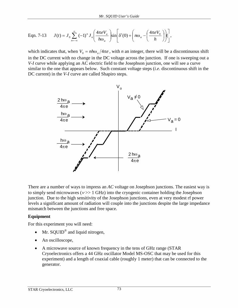
Mr. SQUID User’s Guide
STAR Cryoelectronics, LLC 73
Eqn. 7-13 ∑∞
−∞=
π
−ω+δ′
ω
π−=
na
a
an
n theV
nh
eVJJtJ 0
04
)0(sin4
)1()( ,
which indicates that, when enhV a πω= 40 , with n an integer, there will be a discontinuous shift in the DC current with no change in the DC voltage across the junction. If one is sweeping out a V-I curve while applying an AC electric field to the Josephson junction, one will see a curve similar to the one that appears below. Such constant voltage steps (i.e. discontinuous shift in the DC current) in the V-I curve are called Shapiro steps.
V
I
V a = 0 h ω 4πe
a
h ω 4πe
a 2
h ω 4πe
a
h ω 4πe
a 2
V a = 0 /
o
There are a number of ways to impress an AC voltage on Josephson junctions. The easiest way is to simply send microwaves (ν >> 1 GHz) into the cryogenic container holding the Josephson junction. Due to the high sensitivity of the Josephson junctions, even at very modest rf power levels a significant amount of radiation will couple into the junctions despite the large impedance mismatch between the junctions and free space.
Equipment For this experiment you will need:
• Mr. SQUID® and liquid nitrogen,
• An oscilloscope,
• A microwave source of known frequency in the tens of GHz range (STAR Cryoelectronics offers a 44 GHz oscillator Model MS-OSC that may be used for this experiment) and a length of coaxial cable (roughly 1 meter) that can be connected to the generator.
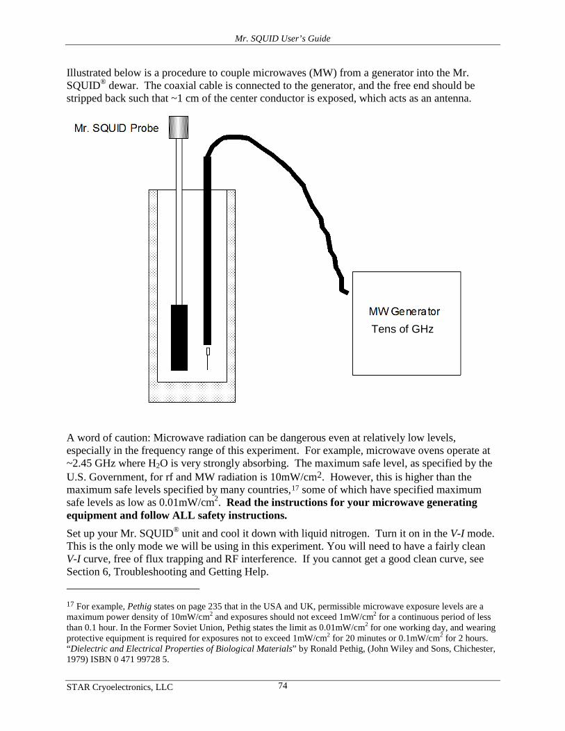
Mr. SQUID User’s Guide
STAR Cryoelectronics, LLC 74
Illustrated below is a procedure to couple microwaves (MW) from a generator into the Mr. SQUID® dewar. The coaxial cable is connected to the generator, and the free end should be stripped back such that ~1 cm of the center conductor is exposed, which acts as an antenna.
A word of caution: Microwave radiation can be dangerous even at relatively low levels, especially in the frequency range of this experiment. For example, microwave ovens operate at ~2.45 GHz where H2O is very strongly absorbing. The maximum safe level, as specified by the U.S. Government, for rf and MW radiation is 10mW/cm2. However, this is higher than the maximum safe levels specified by many countries,17
Set up your Mr. SQUID® unit and cool it down with liquid nitrogen. Turn it on in the V-I mode. This is the only mode we will be using in this experiment. You will need to have a fairly clean V-I curve, free of flux trapping and RF interference. If you cannot get a good clean curve, see Section
some of which have specified maximum safe levels as low as 0.01mW/cm2. Read the instructions for your microwave generating equipment and follow ALL safety instructions.
6, Troubleshooting and Getting Help. 17 For example, Pethig states on page 235 that in the USA and UK, permissible microwave exposure levels are a maximum power density of 10mW/cm2 and exposures should not exceed 1mW/cm2 for a continuous period of less than 0.1 hour. In the Former Soviet Union, Pethig states the limit as 0.01mW/cm2 for one working day, and wearing protective equipment is required for exposures not to exceed 1mW/cm2 for 20 minutes or 0.1mW/cm2 for 2 hours. “Dielectric and Electrical Properties of Biological Materials” by Ronald Pethig, (John Wiley and Sons, Chichester, 1979) ISBN 0 471 99728 5.
Tens of GHz
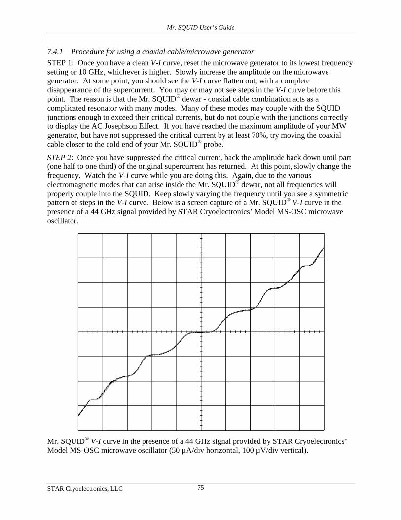
Mr. SQUID User’s Guide
STAR Cryoelectronics, LLC 75
7.4.1 Procedure for using a coaxial cable/microwave generator STEP 1: Once you have a clean V-I curve, reset the microwave generator to its lowest frequency setting or 10 GHz, whichever is higher. Slowly increase the amplitude on the microwave generator. At some point, you should see the V-I curve flatten out, with a complete disappearance of the supercurrent. You may or may not see steps in the V-I curve before this point. The reason is that the Mr. SQUID® dewar - coaxial cable combination acts as a complicated resonator with many modes. Many of these modes may couple with the SQUID junctions enough to exceed their critical currents, but do not couple with the junctions correctly to display the AC Josephson Effect. If you have reached the maximum amplitude of your MW generator, but have not suppressed the critical current by at least 70%, try moving the coaxial cable closer to the cold end of your Mr. SQUID® probe.
STEP 2: Once you have suppressed the critical current, back the amplitude back down until part (one half to one third) of the original supercurrent has returned. At this point, slowly change the frequency. Watch the V-I curve while you are doing this. Again, due to the various electromagnetic modes that can arise inside the Mr. SQUID® dewar, not all frequencies will properly couple into the SQUID. Keep slowly varying the frequency until you see a symmetric pattern of steps in the V-I curve. Below is a screen capture of a Mr. SQUID® V-I curve in the presence of a 44 GHz signal provided by STAR Cryoelectronics’ Model MS-OSC microwave oscillator.
Mr. SQUID® V-I curve in the presence of a 44 GHz signal provided by STAR Cryoelectronics’ Model MS-OSC microwave oscillator (50 µA/div horizontal, 100 µV/div vertical).
Mr. SQUID User’s Guide
STAR Cryoelectronics, LLC 76
Trouble-avoidance tip: If you cannot see any steps in the V-I after tuning the frequency up all the way, go back and repeat step 1 at a slightly higher frequency, then repeat step 2. Due to the spurious electromagnetic modes which form in the Mr. SQUID® dewar due to the silver coating inside the glass dewar, getting the microwaves to couple properly can be somewhat of a “black art”.
7.4.2 Determining e/h To determine the value of e/h, we need to measure the voltage change per step ∆Vo. This can usually be done to greater accuracy by measuring the voltage between a number of steps and then dividing by this number. For example, in the screen shot shown above there are six steps. The vertical setting on the oscilloscope was 1 V/div, which corresponds to 100 µV/div. The voltage difference between the n = +3 and n = -3 steps is about 540 µV, or 90 µV per step.
The voltage change per step is given by
Eqn. 7-14 e
he
nhehnV aaa
o 244)1( ν
πω
πω
=−+
=∆ ,
So that
Eqn. 7-15 02Vh
e aν= .
For our data from above,
Eqn. 7-16 Hertz/Volt1044.2Volts)102(90
Hertz10442
146-
9
0
×≈××
==Vh
e aν
The “official” value of e/h is 2.4179671×10¹⁴ Hertz/Volt, which means our measurement was “good” to about 0.9%. This relatively high level of accuracy using such a simple measurement is the reason the AC Josephson Effect is used by the National Institute of to set the standard for the “official” value of the Volt.
However, for us to claim that we made this measurement to this level of accuracy would be somewhat misleading. The reason is that if you look at the scope picture of the Shapiro steps above, the steps are not perfectly flat and show some rounding. This might be due to small fluctuations in the microwave generator frequency or they might also be due to thermal noise in the SQUID. Remember, although 77 K may seem cold to us, it is rather “hot” compared to the superconducting transition temperature of your SQUID (77 K/Tc ~ 0.85). So there is some uncertainty in the placement of the steps. For a measurement uncertainty of 3 µV (the rough precision to which the step voltage from the screen plot above can be measured), the voltages at which the steps appear would be stated as 90 ±3 µV.
To calculate the uncertainty in a function f(x) from the uncertainty of x, we would use*
*There are many good books on error analysis and error propagation. Two that we recommend are “Introduction to the Theory of Error” by Yardley Beers, (Addison-Wesley, Menlo Park California, 1962) ISBN 0-201-00470-4 and “An Introduction to Error Analysis” by John R. Taylor, (University Science Books, Mill Valley California, 1982) ISBN 0-935702-10-5.
Mr. SQUID User’s Guide
STAR Cryoelectronics, LLC 77
Eqn. 7-17 ( ) 22
)( xf xfx
σ
∂∂
=σ .
This means the 1 µV uncertainty in the voltage step (σV) would result in an uncertainty σe/h for e/h of
Eqn. 7-18 22
/ Vhe he
Vσ
∂∂
=σ
where σV = 3 µV.
Then,
Eqn. 7-19 Hz/V101.63V103)V10(90
Hz1044 13626-
9
20
/ ×≈×⋅××
=≈ −V
ahe V
σνσ
Our value for e/h is then (2.44 ± 0.16)×1014 Hz/V, as compared to the “official value” of 2.4179671×10¹⁴ Hz/V, which means we really have about a 6% uncertainty in our measurement. One can increase the accuracy of this measurement by cooling the SQUID to reduce the thermal rounding of the steps, by stabilizing the microwave source so that its frequency does not fluctuate, and shielding the SQUID from RF interferences (other than the microwave source) which can also cause rounding of the steps. By doing all these things, the ratio of value for e/h has been determined to a large number of decimal places.18
18W.H. Parker, B.N. Taykor, and D.N. Langenburg, Phys. Rev. Letters 18, 287 (1967).
Since ultra-stable frequency sources are relatively easy to build (e.g. atomic clocks), the U.S. National Institute of Standards (NIST) uses such time references along with the AC Josephson Effect to set the standard for the “official” value of the volt.

Mr. SQUID User’s Guide
STAR Cryoelectronics, LLC 78
7.5 Inductive Measurement of the Superconducting Transition Temperature of an HTS Film
Purpose SQUIDs, by virtue of being the world’s most sensitive detectors of magnetic fields, are commonly used in instruments designed to measure the magnetic properties of materials. Knowing the magnetic behavior of a material is often of direct technological importance as in the case of metals and oxides used for magnetic recording. The magnetic behavior of a material is often an indicator of its electronic properties, as in the case of the Meissner effect in superconductivity. In this experiment, we will measure the ability of a superconducting film to expel magnetic flux as it undergoes a superconducting transition.
Equipment For this experiment you will need:
• A HTS thin-film grown on sapphire19
• Mr. SQUID® and liquid nitrogen,
at least 0.5cm × 0.5 cm in size,
• An oscilloscope or X-Y recorder,
• One glass encapsulated silicon diode (e.g., 1N914 or equivalent),
• One 100 Ω surface mount thin film chip resistor,
• 500 cm of copper wire of size 36 to 40 AWG insulated magnet wire20
• A digital volt meter (DVM) with sub-millivolt resolution,
(this corresponds to diameters of 0.013 to 0.08 mm),
21
• A second digital volt meter (DVM) (may be a “hand held” unit),
• A 0-10 Volt adjustable power supply,
• A decade resistor box with resistance values from below 100 Ω to above 100 kΩ,
• A low frequency sine wave generator capable of frequencies below 2.5 kHz,
• A soldering iron and electronics grade solder,
• Polystyrene cement (“model glue”) such as Duco Cement,22
• One binder clip,
• Aluminum foil,
19This experiment works best if the HTS film is on a high thermal conductivity substrate such as sapphire. Although any size chip greater than 0.5 cm × 0.5 cm will do, it will be easier to mount the coil, diode and resistor on a 1cm × 1cm chip. YBCO films on sapphire are available from STAR Cryoelectronics. 20Such as Belden Beldsol Solderable Magnet Wire Types 8081 through 8087. 21Such as a Kiethley Model 197 or Agilent 34401A digital voltmeter. Millivolt resolution may be acceptable but will limit the accuracy of the temperature measurements. 22Any polystyrene cement (“model glue”) will work. If none is available, clear finger nail polish will work. Duco Cement is a registered trademark of the Devcon Corporation, Wood Dale, IL 60191, U.S.A.
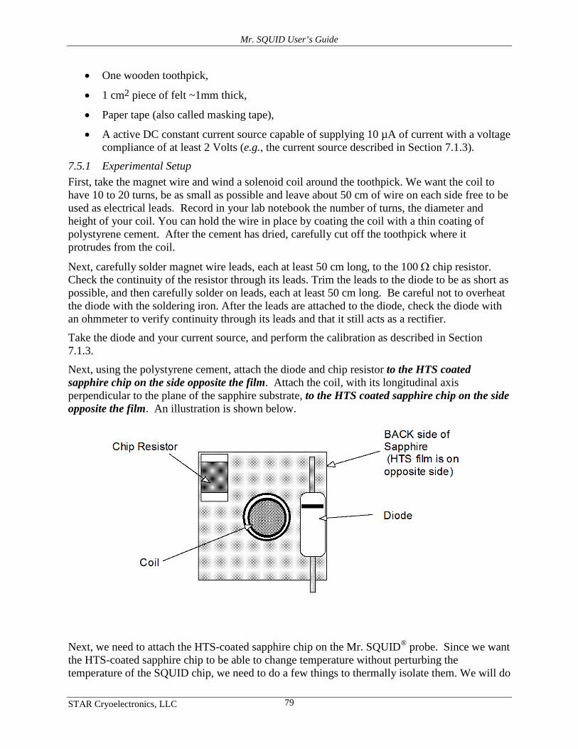
Mr. SQUID User’s Guide
STAR Cryoelectronics, LLC 79
• One wooden toothpick,
• 1 cm2 piece of felt ~1mm thick,
• Paper tape (also called masking tape),
• A active DC constant current source capable of supplying 10 µA of current with a voltage compliance of at least 2 Volts (e.g., the current source described in Section 7.1.3).
7.5.1 Experimental Setup First, take the magnet wire and wind a solenoid coil around the toothpick. We want the coil to have 10 to 20 turns, be as small as possible and leave about 50 cm of wire on each side free to be used as electrical leads. Record in your lab notebook the number of turns, the diameter and height of your coil. You can hold the wire in place by coating the coil with a thin coating of polystyrene cement. After the cement has dried, carefully cut off the toothpick where it protrudes from the coil.
Next, carefully solder magnet wire leads, each at least 50 cm long, to the 100 Ω chip resistor. Check the continuity of the resistor through its leads. Trim the leads to the diode to be as short as possible, and then carefully solder on leads, each at least 50 cm long. Be careful not to overheat the diode with the soldering iron. After the leads are attached to the diode, check the diode with an ohmmeter to verify continuity through its leads and that it still acts as a rectifier.
Take the diode and your current source, and perform the calibration as described in Section 7.1.3.
Next, using the polystyrene cement, attach the diode and chip resistor to the HTS coated sapphire chip on the side opposite the film. Attach the coil, with its longitudinal axis perpendicular to the plane of the sapphire substrate, to the HTS coated sapphire chip on the side opposite the film. An illustration is shown below.
Next, we need to attach the HTS-coated sapphire chip on the Mr. SQUID® probe. Since we want the HTS-coated sapphire chip to be able to change temperature without perturbing the temperature of the SQUID chip, we need to do a few things to thermally isolate them. We will do
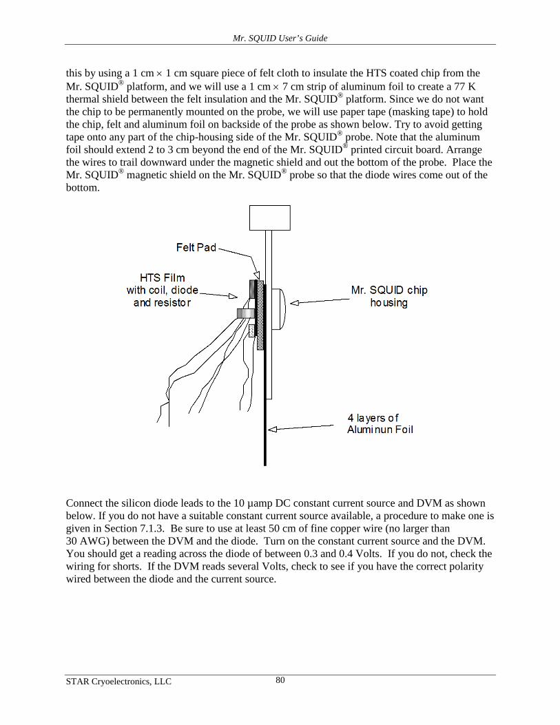
Mr. SQUID User’s Guide
STAR Cryoelectronics, LLC 80
this by using a 1 cm × 1 cm square piece of felt cloth to insulate the HTS coated chip from the Mr. SQUID® platform, and we will use a 1 cm × 7 cm strip of aluminum foil to create a 77 K thermal shield between the felt insulation and the Mr. SQUID® platform. Since we do not want the chip to be permanently mounted on the probe, we will use paper tape (masking tape) to hold the chip, felt and aluminum foil on backside of the probe as shown below. Try to avoid getting tape onto any part of the chip-housing side of the Mr. SQUID® probe. Note that the aluminum foil should extend 2 to 3 cm beyond the end of the Mr. SQUID® printed circuit board. Arrange the wires to trail downward under the magnetic shield and out the bottom of the probe. Place the Mr. SQUID® magnetic shield on the Mr. SQUID® probe so that the diode wires come out of the bottom.
Connect the silicon diode leads to the 10 µamp DC constant current source and DVM as shown below. If you do not have a suitable constant current source available, a procedure to make one is given in Section 7.1.3. Be sure to use at least 50 cm of fine copper wire (no larger than 30 AWG) between the DVM and the diode. Turn on the constant current source and the DVM. You should get a reading across the diode of between 0.3 and 0.4 Volts. If you do not, check the wiring for shorts. If the DVM reads several Volts, check to see if you have the correct polarity wired between the diode and the current source.
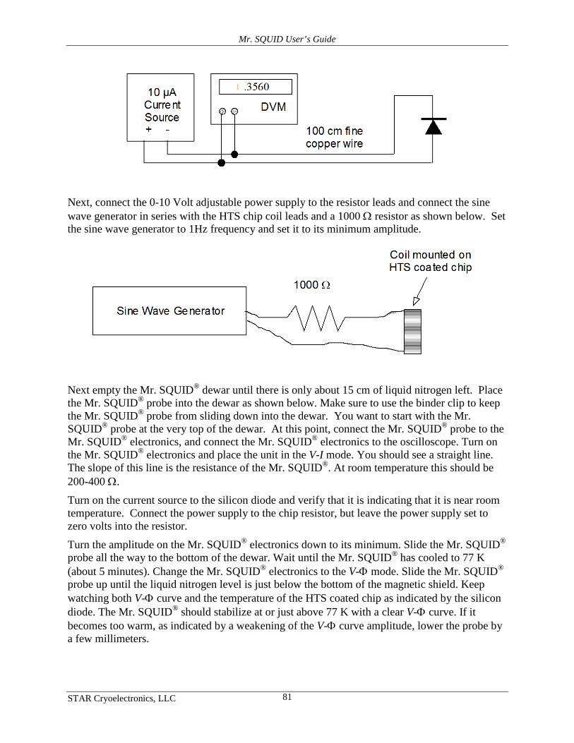
Mr. SQUID User’s Guide
STAR Cryoelectronics, LLC 81
Next, connect the 0-10 Volt adjustable power supply to the resistor leads and connect the sine wave generator in series with the HTS chip coil leads and a 1000 Ω resistor as shown below. Set the sine wave generator to 1Hz frequency and set it to its minimum amplitude.
Next empty the Mr. SQUID® dewar until there is only about 15 cm of liquid nitrogen left. Place the Mr. SQUID® probe into the dewar as shown below. Make sure to use the binder clip to keep the Mr. SQUID® probe from sliding down into the dewar. You want to start with the Mr. SQUID® probe at the very top of the dewar. At this point, connect the Mr. SQUID® probe to the Mr. SQUID® electronics, and connect the Mr. SQUID® electronics to the oscilloscope. Turn on the Mr. SQUID® electronics and place the unit in the V-I mode. You should see a straight line. The slope of this line is the resistance of the Mr. SQUID®. At room temperature this should be 200-400 Ω.
Turn on the current source to the silicon diode and verify that it is indicating that it is near room temperature. Connect the power supply to the chip resistor, but leave the power supply set to zero volts into the resistor.
Turn the amplitude on the Mr. SQUID® electronics down to its minimum. Slide the Mr. SQUID® probe all the way to the bottom of the dewar. Wait until the Mr. SQUID® has cooled to 77 K (about 5 minutes). Change the Mr. SQUID® electronics to the V-Φ mode. Slide the Mr. SQUID® probe up until the liquid nitrogen level is just below the bottom of the magnetic shield. Keep watching both V-Φ curve and the temperature of the HTS coated chip as indicated by the silicon diode. The Mr. SQUID® should stabilize at or just above 77 K with a clear V-Φ curve. If it becomes too warm, as indicated by a weakening of the V-Φ curve amplitude, lower the probe by a few millimeters.
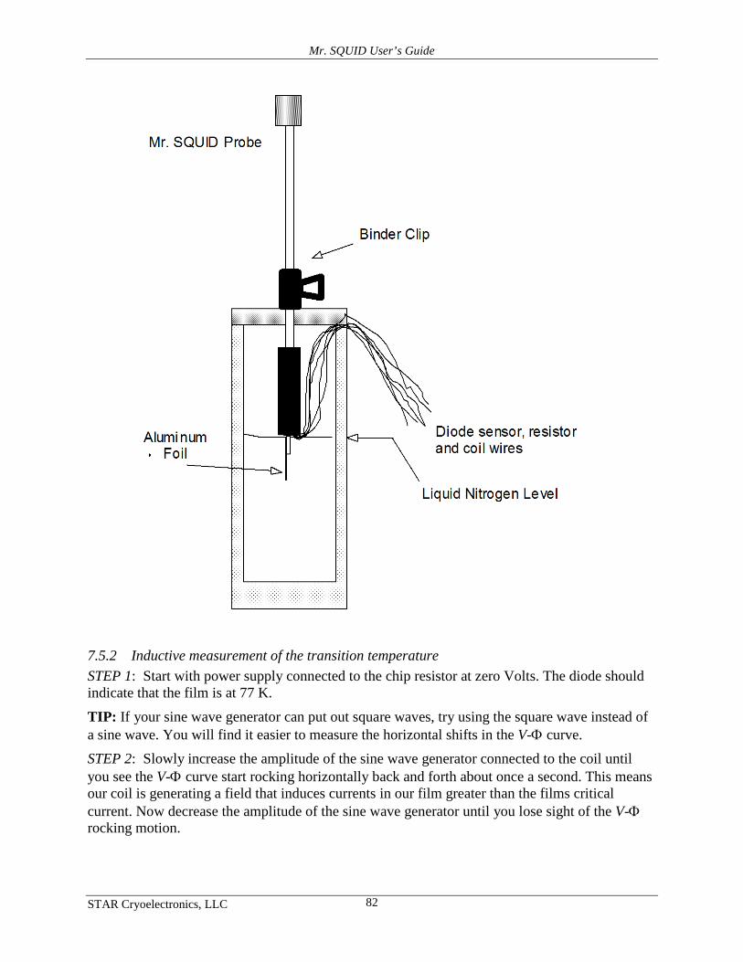
Mr. SQUID User’s Guide
STAR Cryoelectronics, LLC 82
7.5.2 Inductive measurement of the transition temperature STEP 1: Start with power supply connected to the chip resistor at zero Volts. The diode should indicate that the film is at 77 K.
TIP: If your sine wave generator can put out square waves, try using the square wave instead of a sine wave. You will find it easier to measure the horizontal shifts in the V-Φ curve. STEP 2: Slowly increase the amplitude of the sine wave generator connected to the coil until you see the V-Φ curve start rocking horizontally back and forth about once a second. This means our coil is generating a field that induces currents in our film greater than the films critical current. Now decrease the amplitude of the sine wave generator until you lose sight of the V-Φ rocking motion.
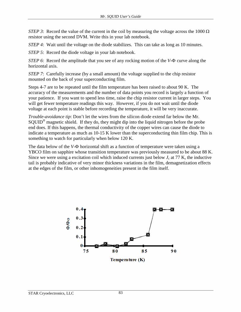
Mr. SQUID User’s Guide
STAR Cryoelectronics, LLC 83
STEP 3: Record the value of the current in the coil by measuring the voltage across the 1000 Ω resistor using the second DVM. Write this in your lab notebook.
STEP 4: Wait until the voltage on the diode stabilizes. This can take as long as 10 minutes. STEP 5: Record the diode voltage in your lab notebook.
STEP 6: Record the amplitude that you see of any rocking motion of the V-Φ curve along the horizontal axis.
STEP 7: Carefully increase (by a small amount) the voltage supplied to the chip resistor mounted on the back of your superconducting film.
Steps 4-7 are to be repeated until the film temperature has been raised to about 90 K. The accuracy of the measurements and the number of data points you record is largely a function of your patience. If you want to spend less time, raise the chip resistor current in larger steps. You will get fewer temperature readings this way. However, if you do not wait until the diode voltage at each point is stable before recording the temperature, it will be very inaccurate.
Trouble-avoidance tip: Don’t let the wires from the silicon diode extend far below the Mr. SQUID® magnetic shield. If they do, they might dip into the liquid nitrogen before the probe end does. If this happens, the thermal conductivity of the copper wires can cause the diode to indicate a temperature as much as 10-15 K lower than the superconducting thin film chip. This is something to watch for particularly when below 120 K.
The data below of the V-Φ horizontal shift as a function of temperature were taken using a YBCO film on sapphire whose transition temperature was previously measured to be about 88 K. Since we were using a excitation coil which induced currents just below Jc at 77 K, the inductive tail is probably indicative of very minor thickness variations in the film, demagnetization effects at the edges of the film, or other inhomogeneities present in the film itself.

Mr. SQUID User’s Guide
STAR Cryoelectronics, LLC 84
7.5.3 Additional exercises for this experiment 1. Calculate, from the geometry of their coils and the values of the currents measured in step 3 above, what size magnetic fields are being used to “sense” the superconducting state of the film.
2. Repeat this experiment using increasing current levels in the coil. Why are the curves different?

Mr. SQUID User’s Guide
STAR Cryoelectronics, LLC 85
7.6 SQUID Properties in Pumped Liquid Nitrogen Purpose Although Mr. SQUID® is designed to show excellent superconducting properties at 77 K in liquid nitrogen, it must be remembered that this operating temperature is about 85% of the critical temperature of 90 K for YBCO. Many of the superconducting properties of Josephson junctions, such as Ic, scale with the parameter (1-t)2 where t is the dimensionless reduced temperature defined as t = T/Tc.
Liquid nitrogen boils at 77 K at atmospheric pressure. By decreasing the ambient pressure, the boiling point can be reduced easily to around 68 K. All of the previous experiments can be done using pumped liquid nitrogen, as most SQUID properties are improved by operation at a lower temperature. The performance of various devices (such as the flux-locked loop and voltmeter) will be improved. In this experiment, we will measure the standard SQUID parameters at this lower reduced temperature, and explore the theory that explains how superconducting properties scale with temperature.
Equipment For this experiment you will need:
• A calibrated silicon diode temperature sensor attached to the Mr. SQUID® probe (see Section 7.1.1 for instructions),
• A >3"-diameter rubber stopper (size number 14) with a hole for tubing (preferably 1/4"),
• A vacuum source capable of less than 100 mTorr over the volume of the Mr. SQUID® dewar (<1 liter).
To design the pumping cap for the Mr. SQUID® dewar, drill a hole in the rubber stopper that is slightly smaller than the outer diameter (O.D.) of the tubing you plan to use. Often cooling the rubber down using liquid nitrogen makes it easier to drill. Insert the tubing so that approximately 1" extends through the hole, and make sure that it is fairly secure (i.e., not easy to pull out).
Fill the dewar about half-full with liquid nitrogen. If you have not yet calibrated your silicon diode temperature sensor, you should do so now. Also, it should be attached to the back of the Mr. SQUID® probe with masking tape. Both of these procedures are described in Advanced Experiment 1 (Section 7.1). At this time, you should record the superconducting parameters of the SQUID at 77 K if you have not already done so.
Now we are ready to pump on the liquid nitrogen to reduce its boiling temperature. Stick the rubber stopper into the top of the Mr. SQUID® dewar with the stopper wide-side towards the Mr. SQUID® dewar as shown in Figure 7-12. Do not use a stopper that enters the Mr. SQUID® dewar! Do not immerse the tubing into the liquid nitrogen inside the dewar!
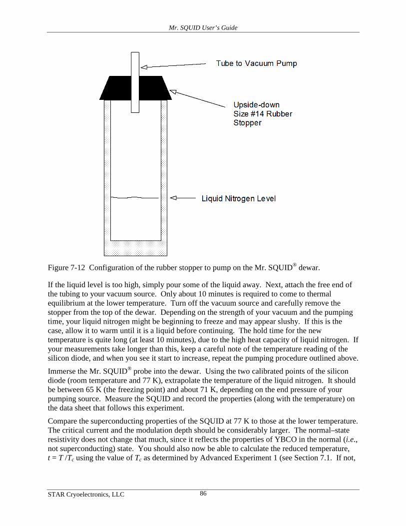
Mr. SQUID User’s Guide
STAR Cryoelectronics, LLC 86
Figure 7-12 Configuration of the rubber stopper to pump on the Mr. SQUID® dewar.
If the liquid level is too high, simply pour some of the liquid away. Next, attach the free end of the tubing to your vacuum source. Only about 10 minutes is required to come to thermal equilibrium at the lower temperature. Turn off the vacuum source and carefully remove the stopper from the top of the dewar. Depending on the strength of your vacuum and the pumping time, your liquid nitrogen might be beginning to freeze and may appear slushy. If this is the case, allow it to warm until it is a liquid before continuing. The hold time for the new temperature is quite long (at least 10 minutes), due to the high heat capacity of liquid nitrogen. If your measurements take longer than this, keep a careful note of the temperature reading of the silicon diode, and when you see it start to increase, repeat the pumping procedure outlined above.
Immerse the Mr. SQUID® probe into the dewar. Using the two calibrated points of the silicon diode (room temperature and 77 K), extrapolate the temperature of the liquid nitrogen. It should be between 65 K (the freezing point) and about 71 K, depending on the end pressure of your pumping source. Measure the SQUID and record the properties (along with the temperature) on the data sheet that follows this experiment.
Compare the superconducting properties of the SQUID at 77 K to those at the lower temperature. The critical current and the modulation depth should be considerably larger. The normal–state resistivity does not change that much, since it reflects the properties of YBCO in the normal (i.e., not superconducting) state. You should also now be able to calculate the reduced temperature, t = T /Tc using the value of Tc as determined by Advanced Experiment 1 (see Section 7.1. If not,
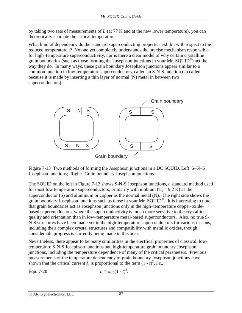
Mr. SQUID User’s Guide
STAR Cryoelectronics, LLC 87
by taking two sets of measurements of Ic (at 77 K and at the new lower temperature), you can theoretically estimate the critical temperature.
What kind of dependency do the standard superconducting properties exhibit with respect to the reduced temperature t? No one yet completely understands the precise mechanism responsible for high–temperature superconductivity, nor is there a clear model of why certain crystalline grain boundaries (such as those forming the Josephson junctions in your Mr. SQUID®) act the way they do. In many ways, these grain boundary Josephson junctions appear similar to a common junction in low-temperature superconductors, called an S-N-S junction (so called because it is made by inserting a thin layer of normal (N) metal in between two superconductors).
N
N S S
S S
S S
S S
Grain boundary
Grain boundary
Figure 7-13 Two methods of forming the Josephson junctions in a DC SQUID. Left S–N–S Josephson junctions; Right: Grain boundary Josephson junctions.
The SQUID on the left in Figure 7-13 shows S-N-S Josephson junctions, a standard method used for most low temperature superconductors, primarily with niobium (Tc = 9.2 K) as the superconductor (S) and aluminum or copper as the normal metal (N). The right side shows the grain boundary Josephson junctions such as those in your Mr. SQUID®. It is interesting to note that grain boundaries act as Josephson junctions only in the high–temperature copper-oxide-based superconductors, where the superconductivity is much more sensitive to the crystalline quality and orientation than in low–temperature metal-based superconductors. Also, no true S-N-S structures have been made yet in the high-temperature superconductors for various reasons, including their complex crystal structures and compatibility with metallic oxides, though considerable progress is currently being made in this area.
Nevertheless, there appear to be many similarities in the electrical properties of classical, low-temperature S-N-S Josephson junctions and high-temperature grain boundary Josephson junctions, including the temperature dependence of many of the critical parameters. Previous measurements of the temperature dependency of grain boundary Josephson junctions have shown that the critical current Ic is proportional to the term (1 - t)2, i.e.,
Eqn. 7-20 Ic = α (1 - t)2.
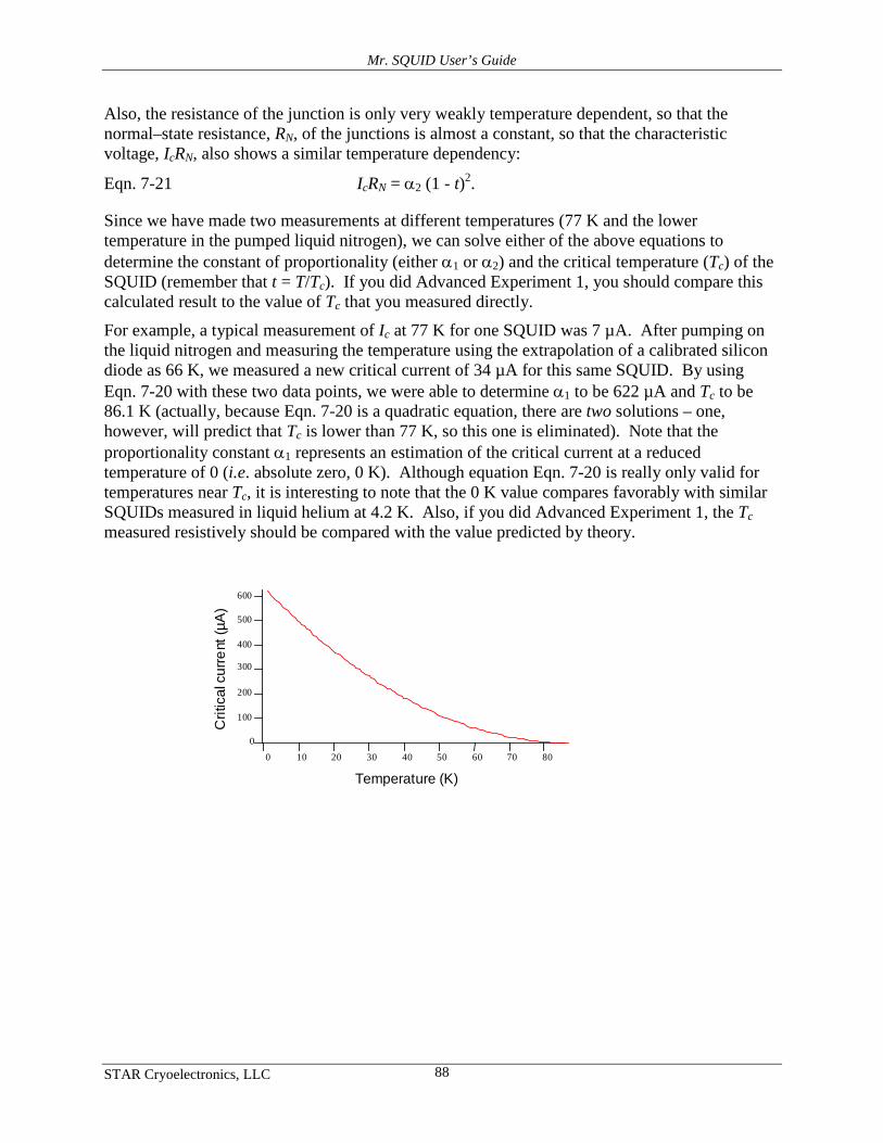
Mr. SQUID User’s Guide
STAR Cryoelectronics, LLC 88
Also, the resistance of the junction is only very weakly temperature dependent, so that the normal–state resistance, RN, of the junctions is almost a constant, so that the characteristic voltage, IcRN, also shows a similar temperature dependency:
Eqn. 7-21 IcRN = α2 (1 - t)2.
Since we have made two measurements at different temperatures (77 K and the lower temperature in the pumped liquid nitrogen), we can solve either of the above equations to determine the constant of proportionality (either α1 or α2) and the critical temperature (Tc) of the SQUID (remember that t = T/Tc). If you did Advanced Experiment 1, you should compare this calculated result to the value of Tc that you measured directly.
For example, a typical measurement of Ic at 77 K for one SQUID was 7 µA. After pumping on the liquid nitrogen and measuring the temperature using the extrapolation of a calibrated silicon diode as 66 K, we measured a new critical current of 34 µA for this same SQUID. By using Eqn. 7-20 with these two data points, we were able to determine α1 to be 622 µA and Tc to be 86.1 K (actually, because Eqn. 7-20 is a quadratic equation, there are two solutions – one, however, will predict that Tc is lower than 77 K, so this one is eliminated). Note that the proportionality constant α1 represents an estimation of the critical current at a reduced temperature of 0 (i.e. absolute zero, 0 K). Although equation Eqn. 7-20 is really only valid for temperatures near Tc, it is interesting to note that the 0 K value compares favorably with similar SQUIDs measured in liquid helium at 4.2 K. Also, if you did Advanced Experiment 1, the Tc measured resistively should be compared with the value predicted by theory.
0
100
200
300 400
500
600
Crit
ical
cur
rent
(µA
)
0 10 20 30 40 50 60 70 80 Temperature (K)
Mr. SQUID User’s Guide
STAR Cryoelectronics, LLC 89
8 ABOUT STAR CRYOELECTRONICS
STAR Cryoelectronics is engaged in the business of producing and marketing advanced sensors based on superconductors and related sensor control electronics. Application areas for STAR products include biomedical imaging, non-destructive testing of materials, geophysical exploration, and laboratory instrumentation. STAR Cryoelectronics manufactures and offers Mr. SQUID® under license from Conductus, Inc.
The cryogenic sensors from STAR Cryoelectronics are based on superconductors and typically operate in liquid nitrogen or in liquid helium. The basic sensor element is a Superconducting Quantum Interference Device (SQUID), which is the most sensitive detector of magnetic flux known. Aside from precision measurements of minute magnetic fields or field gradients, a SQUID may be used to measure any physical quantity that can be converted to a magnetic field, such as electrical currents or voltages, magnetic susceptibility, physical displacement, etc.
In addition to the extensive sensor product line, STAR Cryoelectronics also offers a line of advanced PC-based sensor control electronics sold under the trade name pcSQUID™. The state-of-the-art control electronics are easy to use and offer the user unsurpassed flexibility and performance. STAR Cryoelectronics’ pcSQUID™ and Mr. SQUID® products are CE-certified.
STAR Cryoelectronics staff and contract consultants include four members of the former Conductus SQUID Technology Group. Production, sales and customer service are handled through the company’s headquarters in Santa Fe, NM. The company’s commercial facilities include about 6,000 square feet of space for research and design development, production, final assembly and test of product, shipping, and sales and marketing activities. STAR Cryoelectronics was formed as a limited liability company in the State of New Mexico in April 1999.
For further information about STAR Cryoelectronics and the advanced SQUID products offered by STAR Cryoelectronics, please visit the company web site, http://www.starcryo.com.
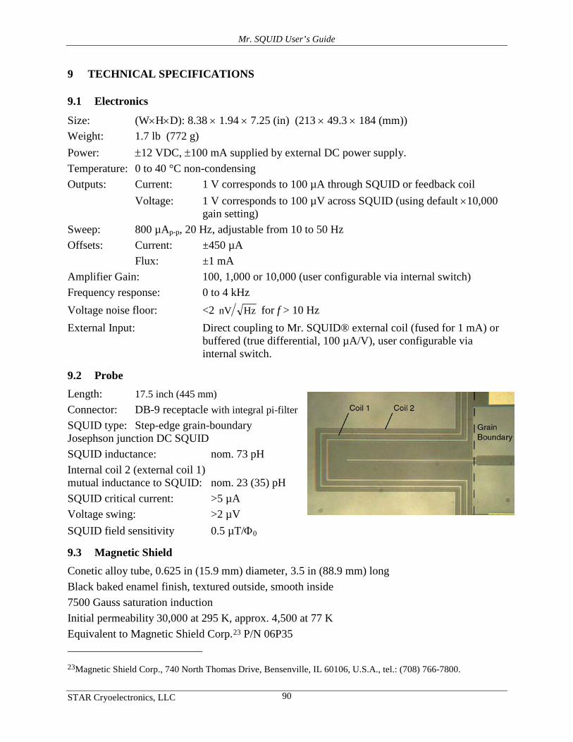
Mr. SQUID User’s Guide
STAR Cryoelectronics, LLC 90
9 TECHNICAL SPECIFICATIONS
9.1 Electronics
Size: (W×H×D): 8.38 × 1.94 × 7.25 (in) (213 × 49.3 × 184 (mm)) Weight: 1.7 lb (772 g) Power: ±12 VDC, ±100 mA supplied by external DC power supply. Temperature: 0 to 40 °C non-condensing Outputs: Current: 1 V corresponds to 100 µA through SQUID or feedback coil Voltage: 1 V corresponds to 100 µV across SQUID (using default ×10,000 gain setting) Sweep: 800 µAp-p, 20 Hz, adjustable from 10 to 50 Hz Offsets: Current: ±450 µA Flux: ±1 mA Amplifier Gain: 100, 1,000 or 10,000 (user configurable via internal switch) Frequency response: 0 to 4 kHz Voltage noise floor: <2 HznV for f > 10 Hz External Input: Direct coupling to Mr. SQUID® external coil (fused for 1 mA) or buffered (true differential, 100 µA/V), user configurable via internal switch.
9.2 Probe Length: 17.5 inch (445 mm) Connector: DB-9 receptacle with integral pi-filter SQUID type: Step-edge grain-boundary Josephson junction DC SQUID SQUID inductance: nom. 73 pH Internal coil 2 (external coil 1) mutual inductance to SQUID: nom. 23 (35) pH SQUID critical current: >5 µA Voltage swing: >2 µV SQUID field sensitivity 0.5 µT/Φ0
9.3 Magnetic Shield Conetic alloy tube, 0.625 in (15.9 mm) diameter, 3.5 in (88.9 mm) long Black baked enamel finish, textured outside, smooth inside 7500 Gauss saturation induction Initial permeability 30,000 at 295 K, approx. 4,500 at 77 K Equivalent to Magnetic Shield Corp.23
23Magnetic Shield Corp., 740 North Thomas Drive, Bensenville, IL 60106, U.S.A., tel.: (708) 766-7800.
P/N 06P35
Mr. SQUID User’s Guide
STAR Cryoelectronics, LLC 91
9.4 RF Filter Module DB-9 M/F EMI filtered connector adapter Each line contains a 0.8 MHz, 4,000 pF low-pass pi-filter Equivalent to Spectrum Control, Inc. 24
9.5 Cable
P/N SCI-56-705-005-LI
DB-9 M/M, 2 m long Equivalent to Assmann Electronics P/N AK129-2-R
9.6 Dewar Aluminum-encased silvered glass vacuum flask Volume: 1000 mL ID: 2.75 in (70 mm) Height: 13.3 in (337 mm) Includes foam cap with slot and hole for supporting the Mr. SQUID® probe Equivalent to Pope Scientific Corp.25
9.7 Rear Panel I/O Specifications
P/N 8645/0099
9.7.1 POWER Pin Description 1 Analog ground 2 Integrator balance offset signal (for MS-FLL Flux-Locked Loop accessory) 3 4 -12 VDC 5 +12 VDC
9.7.2 PROBE Pin Description 1 +V 2 -V 3 +I 4 -I 5 +Iint (internal feedback) 6 -Iint (internal feedback) 7 +Iext (externalfeedback) 8 -Iext (external feedback) 9 Analog ground
24Spectrum Controls, Inc. 2185 West Eighth Street, Erie PA 16505, U.S.A., tel.: (814) 455-0966. 25Pope Scientific Corp., N90 W14337 Commerce Drive, P.O. Box 495, Menomonee Falls, WI 53051, U.S.A., tel.: (414) 251-9300.

Mr. SQUID User’s Guide
STAR Cryoelectronics, LLC 92
9.7.3 EXT INPUT BNC connector to couple a voltage signal to the external feedback coil. A MODE switch inside the Mr. SQUID® electronics box (accessible by removing the top cover) selects whether this signal is routed directly through a 100 mA fuse at location F1 inside the box to the external feedback coil (switch position DIR) or is converted to true differential using a buffer amplifier and then routed to the feedback coil (switch position BUF). The current output from the buffer amplifier (i.e., the current applied to the external feedback coil) is 100 µA/V. The buffered configuration is the default set at the factory.
9.7.4 OUTPUT Buffered single-ended outputs of all SQUID signals (SQUID bias current (I), SQUID output voltage (V), internal feedback coil current (Iint), and external feedback coil current (Iext)). The pinouts and scaling are summarized in the table below. The signals at the OUTPUT connector can be connected to the optional MS-DAQ14 or MS-DAQ16 USB Mr. SQUID® Digitizer to display the SQUID V-I and V-Φ characteristics on a computer. The Mr. SQUID® Digitizer software simplifies measurements of the SQUID parameters (Ic, RN, ∆V, ∆Im) and transfer function (dV/dΦ).
Pin Description Scaling 1 SQUID output voltage, V 10,000 (default)¹ 2 Internal feedback coil current, Iint 100 µA/V 3 SQUID bias current, I 100 µA/V 4 External feedback coil current, Iext 100 µA/V 5 6 7 8 Analog ground 9 Analog ground 10 Analog ground 11 Analog ground 12 Analog ground 13 14 15 Analog ground ¹May be configured for a scaling factor of 100, 1,000 or 10,000 using a gain switch inside the Mr. SQUID® electronics box accessible by removing the top cover.
The above specifications are effective 1/11/2010 and subject to change without prior notice.
Mr. SQUID User’s Guide
STAR Cryoelectronics, LLC 93
10 REFERENCES
Most of the available information on superconductive electronics in general and on SQUIDs in particular is in the professional scientific literature. However, there are a number of texts and popularizations available that can serve as sources of information beyond what is provided in this User's Guide. Also included are some technical review articles and papers that discuss SQUID operation and applications.
Popularization “Superconductors: Conquering technology's new frontier,” Randy Simon and Andrew Smith, Plenum Publishing (New York) 1988
A non-mathematical presentation of the history, physics, and applications of superconductivity up to and including the discovery of high-temperature superconductivity.
Texts “Foundations of Applied Superconductivity,” Terry Orlando and Kevin Delin, Addison-Wesley Publishing Co. (Reading, MA) 1991
The new standard text on the principles of superconducting applications both thin film and bulk written in the post-high-Tc era and incorporating the consequences of the new materials.
“Introduction to Superconductivity,” Michael Tinkham, McGraw-Hill, Inc. (New York) 1975
A classic text on the science of superconductivity geared to upper division undergraduates and graduate students. Written before the high-Tc discovery.
“Superconductivity of Metals and Alloys,” P.G. de Gennes, Addison-Wesley Publishing Co. (Reading, MA) 1966, 1989
THE classic monograph on superconductivity. Reissued in 1989 with corrections by de Gennes. Geared to upper division undergraduates and graduate students. A “must” for serious researchers. Written before the high-Tc discovery.
“Introduction to Superconductivity,” A.C. Rose-Innes and E.H. Rhoderick, International Series in Solid State Physics, Vol. 6, Pergamon Press (Oxford) 1978
Written at more accessible level, this text focuses on explaining the experimental effects of superconductors. Written before the high- Tc discovery.
“Principles of Superconductive Devices and Circuits,” Theodore Van Duzer and Charles Turner, Elsevier North-Holland, Inc. (New York) 1981
The standard text on superconductive electronics with an emphasis on the physics of the electronic devices. Written before the high-Tc discovery.
“A Seminar on Superconductivity,” Ch. 21 from The Feynman Lectures on Physics, Vol. III, Richard P. Feynman, Robert B. Leighton, and Matthew Sands, Addison-Wesley Publishing Co. (Reading, MA) 1965
An early treatment of the quantum nature of superconductivity, including the original data and interpretation of some of the first devices to show quantum interference. Written before the high-Tc discovery.
Mr. SQUID User’s Guide
STAR Cryoelectronics, LLC 94
Articles and Technical Papers General Audience
“Superconductivity,” Kevin A. Delin and Terry P. Orlando, The Electrical Engineering Handbook, R.C. Dorf ed., pp 1114-1123, (CRC Press, Cleveland OH 1993)
This is a short overview of superconductivity at an undergraduate level.
“SQUIDs, brains and gravity waves,” John Clarke, Physics Today, March 1986, pp. 36-44.
Written just before the advent of the high-Tc cuprate superconductors, this is an accessible account of low-Tc DC SQUIDs and some of their applications.
“Principles and applications of SQUIDs,” John Clarke, Proc. IEEE 77, pp. 1208-1223 (1989).
A more comprehensive account of both low- and high-Tc SQUIDs.
“The impact of high-temperature superconductivity on SQUID magnetometers,” John Clarke and Roger H. Koch, Science 242, pp.217-223 (1988).
Discusses some early high- Tc SQUIDs and compares their performance with that of other kinds of magnetometers.
Advanced Topics
“DC SQUID: Noise and optimization,” Claudia D. Tesche and John Clarke, Journal of Low Temperature Physics 29, pp. 301-331 (1977).
This technical paper sets out the results of an extensive computer simulation of the operation of the DC SQUID.
“SQUID magnetometers for low-frequency applications,” Tapani Ryhänen, Heikki Seppa, Risto Ilmoniemi and Jukka Knuutila, Journal of Low Temperature Physics 76, pp.287-386 (1989).
A long review describing many kinds of SQUIDs and their applications.
“Radio-frequency SQUID operation using a ceramic high-temperature superconductor,” M.S. Colclough, C.E. Gough, M. Keene, C.M. Muirhead, N. Thomas, J.S. Abell and S. Sutton; Nature 328, 47-48 (1987).
The first SQUID magnetometer made with a high-Tc superconductor.
“Noise characteristics of single grain boundary junction DC SQUIDs in Y1Ba2Cu3O7-d films,” R. Gross, P. Chaudhari, M. Kawasaki, M. Ketchen, A. Gupta, Physica C 170, 315 (1990)
The first SQUID made using the basic junction technology similar to that used in your Mr. SQUID®.
“Extension of the bi-epitaxial Josephson junction process to various substrates,” K. Char, M.S. Colclough, L.P. Lee and G. Zaharchuk; App. Phys. Lett. 59, 2177-2179 (1991).
A detailed description of the technology used in making the older (pre-June 1995) Mr. SQUID® chips.

Mr. SQUID User’s Guide
STAR Cryoelectronics, LLC 95