
MOTOROLA SEMICONDUCTOR TECHNICAL DATA DSP56303
174
MOTOROLA SEMICONDUCTOR TECHNICAL DATA DSP56303 Order this document by: DSP56303/D ©1996, 1997 MOTOROLA, INC. Preliminary Data This document contains information on a new product. Specifications and information herein are subject to change without notice. Advance Information 24-BIT GENERAL PURPOSE DIGITAL SIGNAL PROCESSOR The DSP56303 is a member of the DSP56300 core family of programmable CMOS Digital Signal Processors (DSPs). This family uses a high performance, single-clock-cycle-per-instruction engine providing a two-fold performance increase over Motorola’s popular DSP56000 core, while retaining code compatibility. Significant architectural enhancements in the DSP56300 family include a barrel shifter, 24-bit addressing, instruction cache, and Direct Memory Access (DMA). The DSP56303 offers 66/80/100 MIPS using an internal 66/80/100 MHz clock at 3.0–3.6 V. The DSP56300 core family offers a new level of performance in speed and power provided by its rich instruction set and low power dissipation, enabling a new generation of wireless, telecommunications, and multimedia products. Figure 1 DSP56303 Block Diagram PLL OnCE™ Clock Generator Internal Data Bus Switch YAB XAB PAB YDB XDB PDB GDB MODB/IRQB MODC/IRQC External Data Bus Switch 13 MODD/IRQD DSP56300 6 16 24-Bit 24 18 DDB DAB Peripheral Core YM_EB XM_EB PM_EB PIO_EB Expansion Area 6 SCI Interface JTAG 5 3 RESET MODA/IRQA PINIT/NMI 2 Boot- strap ROM EXTAL XTAL Address Control Data Triple Timer Host Interface HI08 ESSI Interface Address Generation Unit Six Channel DMA Unit Program Interrupt Controller Program Decode Controller Program Address Generator Data ALU 24 × 24 + 56 → 56-bit MAC Two 56-bit Accumulators 56-bit Barrel Shifter Power Mngmnt. External Bus Interface & I - Cache Control External Address Bus Switch AA0456 Memory Expansion Area DE Program RAM 4096 × 24 (default) X Data RAM 2048 × 24 (default) Y Data RAM 2048 × 24 (default)
Transcript of MOTOROLA SEMICONDUCTOR TECHNICAL DATA DSP56303

MOTOROLASEMICONDUCTOR TECHNICAL DATA
DSP56303
Order this document by:DSP56303/D
©1996, 1997 MOTOROLA, INC.
Preliminary Data
This document contains information on a new product. Specifications and information herein are subject to change without notice.
Advance Information24-BIT GENERAL PURPOSE DIGITAL SIGNAL PROCESSOR
The DSP56303 is a member of the DSP56300 core family of programmable CMOS Digital Signal Processors (DSPs). This family uses a high performance, single-clock-cycle-per-instruction engine providing a two-fold performance increase over Motorola’s popular DSP56000 core, while retaining code compatibility. Significant architectural enhancements in the DSP56300 family include a barrel shifter, 24-bit addressing, instruction cache, and Direct Memory Access (DMA). The DSP56303 offers 66/80/100 MIPS using an internal 66/80/100 MHz clock at 3.0–3.6 V. The DSP56300 core family offers a new level of performance in speed and power provided by its rich instruction set and low power dissipation, enabling a new generation of wireless, telecommunications, and multimedia products.
Figure 1 DSP56303 Block Diagram
PLL OnCE™
ClockGenerator
Internal DataBus
Switch
YABXABPAB
YDBXDB
PDB
GDB
MODB/IRQBMODC/IRQC
ExternalData Bus
Switch
13
MODD/IRQD
DSP56300
616
24-Bit
24
18
DDB
DAB
Peripheral
Core
YM
_EB
XM
_EB
PM
_EB
PIO
_EB
Expansion Area
6
SCIInterface
JTAG5
3
RESET
MODA/IRQA
PINIT/NMI
2
Boot-strapROM
EXTAL
XTAL
Address
Control
Data
TripleTimer
HostInterface
HI08
ESSIInterface
AddressGeneration
Unit
Six ChannelDMA Unit
ProgramInterrupt
Controller
ProgramDecode
Controller
ProgramAddress
Generator
Data ALU24 × 24 + 56 → 56-bit MAC
Two 56-bit Accumulators56-bit Barrel Shifter
PowerMngmnt.
ExternalBus
Interface &
I - CacheControl
ExternalAddress
BusSwitch
AA0456
MemoryExpansion
Area
DE
Program RAM4096 × 24(default)
X DataRAM
2048 × 24(default)
Y DataRAM
2048 × 24(default)

Preliminary Data
ii DSP56303/D, Rev. 1 MOTOROLA
TABLE OF CONTENTS
SECTION 1 SIGNAL/CONNECTION DESCRIPTIONS. . . . . . . . . . . . . . . . . . . . .1-1
SECTION 2 SPECIFICATIONS . . . . . . . . . . . . . . . . . . . . . . . . . . . . . . . . . . . . . . .2-1
SECTION 3 PACKAGING . . . . . . . . . . . . . . . . . . . . . . . . . . . . . . . . . . . . . . . . . . .3-1
SECTION 4 DESIGN CONSIDERATIONS . . . . . . . . . . . . . . . . . . . . . . . . . . . . . .4-1
SECTION 5 ORDERING INFORMATION . . . . . . . . . . . . . . . . . . . . . . . . . . . . . . .5-1
APPENDIX A POWER CONSUMPTION BENCHMARK . . . . . . . . . . . . . . . . . . . . A-1
APPENDIX B BOOTSTRAP PROGRAM . . . . . . . . . . . . . . . . . . . . . . . . . . . . . . . . B-1
INDEX . . . . . . . . . . . . . . . . . . . . . . . . . . . . . . . . . . . . . . . . . . . . Index-1
FOR TECHNICAL ASSISTANCE:
Telephone: 1-800-521-6274
Email: [email protected]
Internet: http://www.motorola-dsp.com
Data Sheet Conventions
This data sheet uses the following conventions:
OVERBAR Used to indicate a signal that is active when pulled low (For example, the RESET pin is active when low.)
“asserted” Means that a high true (active high) signal is high or that a low true (active low) signal is low
“deasserted” Means that a high true (active high) signal is low or that a low true (active low) signal is high
Examples: Signal/Symbol Logic State Signal State Voltage1
PIN True Asserted VIL/VOL
PIN False Deasserted VIH/VOH
PIN True Asserted VIH/VOH
PIN False Deasserted VIL/VOL
Note: Values for VIL, VOL, VIH, and VOH are defined by individual product specifications.

DSP56303
Features
Preliminary Data
MOTOROLA DSP56303/D, Rev. 1 iii
FEATURES
High Performance DSP56300 Core
• 66/80/100 Million Instructions Per Second (MIPS) with a 66/80/100 MHz clock at 3.0–3.6 V
• Object code compatible with the DSP56000 core
• Highly parallel instruction set
• Data Arithmetic Logic Unit (Data ALU)
– Fully pipelined 24 x 24-bit parallel Multiplier-Accumulator (MAC)
– 56-bit parallel barrel shifter (fast shift and normalization; bit stream generation and parsing)
– Conditional ALU instructions
– 24-bit or 16-bit arithmetic support under software control
• Program Control Unit (PCU)
– Position Independent Code (PIC) support
– Addressing modes optimized for DSP applications (including immediate offsets)
– On-chip instruction cache controller
– On-chip memory-expandable hardware stack
– Nested hardware DO loops
– Fast auto-return interrupts
• Direct Memory Access (DMA)
– Six DMA channels supporting internal and external accesses
– One-, two-, and three- dimensional transfers (including circular buffering)
– End-of-block-transfer interrupts
– Triggering from interrupt lines and all peripherals
• Phase Lock Loop (PLL)
– Allows change of low power Divide Factor (DF) without loss of lock
– Output clock with skew elimination

Preliminary Data
iv DSP56303/D, Rev. 1 MOTOROLA
DSP56303
Features
• Hardware debugging support
– On-Chip Emulation (OnCE) module
– Joint Action Test Group (JTAG) Test Access Port (TAP)
– Address Trace mode reflects internal Program RAM accesses at the external port
On-Chip Memories
• Program RAM, Instruction Cache, X data RAM, and Y data RAM size is programmable:
• 192 x 24-bit bootstrap ROM
Off-Chip Memory Expansion
• Data memory expansion to two 256 K × 24-bit word memory spaces (or up to two 4 M x 24-bit word memory spaces by using the Address Attribute AA0–AA3 signals)
• Program memory expansion to one 256 K × 24-bit words memory space (or up to one 4 M x 24-bit word memory space by using the Address Attribute AA0–AA3 signals)
• External memory expansion port
• Chip Select Logic for glueless interface to SRAMs
• On-chip DRAM Controller for glueless interface to DRAMs
Instruction Cache
Switch Mode
Program RAM Size
Instruction Cache Size
X Data RAM Size
Y Data RAM Size
disabled disabled 4096 × 24-bit 0 2048 × 24-bit 2048 × 24-bit
enabled disabled 3072 × 24-bit 1024 × 24-bit 2048 × 24-bit 2048 × 24-bit
disabled enabled 2048 × 24-bit 0 3072 × 24-bit 3072 × 24-bit
enabled enabled 1024 × 24-bit 1024 × 24-bit 3072 × 24-bit 3072 × 24-bit

DSP56303
Target Applications
Preliminary Data
MOTOROLA DSP56303/D, Rev. 1 v
On-Chip Peripherals
• Enhanced DSP56000-like 8-bit parallel Host Interface (HI08) supports a variety of buses (e.g., ISA) and provides glueless connection to a number of industry standard microcomputers, microprocessors, and DSPs
• Two Enhanced Synchronous Serial Interfaces (ESSI), each with one receiver and three transmitters (allows six-channel home theater)
• Serial Communications Interface (SCI) with baud rate generator
• Triple timer module
• Up to thirty-four programmable General Purpose Input/Output (GPIO) pins, depending on which peripherals are enabled
Reduced Power Dissipation
• Very low power CMOS design
• Wait and Stop low power standby modes
• Fully-static logic, operation frequency down to 0 Hz (DC)
• Optimized power management circuitry (instruction-dependent, peripheral-dependent, and mode-dependent)
TARGET APPLICATIONS
The DSP56303 is intended for use in telecommunication applications, such as multi-line voice/data/fax processing, videoconferencing, audio applications, control, and general digital signal processing.

Preliminary Data
vi DSP56303/D, Rev. 1 MOTOROLA
DSP56303
Product Documentation
PRODUCT DOCUMENTATION
The three documents listed in the following table are required for a complete description of the DSP56303 and are necessary to design properly with the part. Documentation is available from one of the following locations (see back cover for detailed information):
• A local Motorola distributor
• A Motorola semiconductor sales office
• A Motorola Literature Distribution Center
• The World Wide Web (WWW)
See the Additional Support section of the DSP56300 Family Manual for detailed information on the multiple support options available to you.
Table 1 DSP56303 Documentation
Name Description Order Number
DSP56300 Family Manual
Detailed description of the DSP56300 family processor core and instruction set
DSP56300FM/AD
DSP56303 User’s Manual
Detailed functional description of the DSP56303 memory configuration, operation, and register programming
DSP56303UM/AD
DSP56303 Technical Data
DSP56303 features list and physical, electrical, timing, and package specifications
DSP56303/D

Preliminary Data
MOTOROLA DSP56303/D, Rev. 1 1-1
SECTION 1
SIGNAL/CONNECTION DESCRIPTIONS
SIGNAL GROUPINGS
The input and output signals of the DSP56303 are organized into functional groups, as shown in Table 1-1 and as illustrated in Figure 1-1.
The DSP56303 is operated from a 3 V supply; however, some of the inputs can tolerate 5 V. A special notice for this feature is added to the signal descriptions of those inputs.
Figure 1-1 is a diagram of DSP56303 signals by functional group.
Table 1-1 DSP56303 Functional Signal Groupings
Functional GroupNumber of
SignalsDetailed
Description
Power (VCC) 18 Table 1-2
Ground (GND) 19 Table 1-3
Clock 2 Table 1-4
PLL 3 Table 1-5
Address BusPort A1
18 Table 1-6
Data Bus 24 Table 1-7
Bus Control 13 Table 1-8
Interrupt and Mode Control 5 Table 1-9
Host Interface (HI08) Port B2 16 Table 1-11
Enhanced Synchronous Serial Interface (ESSI) Ports C and D3 12 Table 1-12 and Table 1-13
Serial Communication Interface (SCI) Port E4 3 Table 1-14
Timer 3 Table 1-15
JTAG/OnCE Port 6 Table 1-16
Note: 1. Port A signals define the external memory interface port, including the external address bus, data bus, and control signals.
2. Port B signals are the HI08 port signals multiplexed with the GPIO signals. 3. Port C and D signals are the two ESSI port signals multiplexed with the GPIO signals. 4. Port E signals are the SCI port signals multiplexed with the GPIO signals.

Preliminary Data
1-2 DSP56303/D, Rev. 1 MOTOROLA
Signal/Connection Descriptions
Signal Groupings
Figure 1-1 Signals Identified by Functional Group
DSP56303
24
18 ExternalAddress Bus
ExternalData Bus
ExternalBusControl
EnhancedSynchronous Serial
Interface Port 0(ESSI0)2
Timers3
PLL
JTAG/OnCE Port
Power Inputs:PLLInternal LogicAddress BusData BusBus ControlHI08ESSI/SCI/Timer
A0–A17
D0–D23
AA0–AA3/RAS0–RAS3
RDWRTABRBGBB
CASBCLKBCLK
TCKTDITDOTMSTRSTDE
CLKOUTPCAP
PINIT/NMI
VCCPVCCQVCCAVCCDVCCCVCCHVCCS
4
SerialCommunications
Interface (SCI) Port2
4
2
2
Grounds:PLLPLL Internal LogicAddress BusData BusBus ControlHI08ESSI/SCI/Timer
GNDPGNDP1GNDQGNDAGNDDGNDCGNDHGNDS
444
2
Interrupt/Mode
Control
MODA/IRQAMODB/IRQBMODC/IRQCMODD/IRQDRESET
HostInterface
(HI08) Port1
Non-Multiplexed BusH0–H7HA0HA1HA2HCS/HCSSingle DSHRWHDS/HDSSingle HRHREQ/HREQHACK/HACK
RXDTXDSCLK
SC00–SC02SCK0SRD0STD0
TIO0TIO1TIO2
8
3
4
2
EXTALXTAL Clock
EnhancedSynchronous Serial
Interface Port 1(ESSI1)2
SC10–SC12SCK1SRD1STD1
3
Multiplexed BusHAD0–HAD7HAS/HASHA8HA9HA10Double DSHRD/HRDHWR/HWRDouble HRHTRQ/HTRQHRRQ/HRRQ
Port B GPIOPB0–PB7PB8PB9PB10PB13
PB11PB12
PB14PB15
Port E GPIO PE0PE1PE2
Port C GPIOPC0-PC2PC3PC4PC5
Port D GPIOPD0-PD2PD3PD4PD5
Timer GPIOTIO0TIO1TIO2
Port A
4
AA0601
Note: 1. The HI08 port supports a non-multiplexed or a multiplexed bus, single or double Data Strobe (DS), and single or double Host Request (HR) configurations. Since each of these modes is configured independently, any combination of these modes is possible. These HI08 signals can also be configured alternately as GPIO signals (PB0–PB15). Signals with dual designations (e.g., HAS/HAS) have configurable polarity.
2. The ESSI0, ESSI1, and SCI signals are multiplexed with the Port C GPIO signals (PC0–PC5), Port D GPIO signals (PD0–PD5), and Port E GPIO signals (PE0–PE2), respectively.
3. TIO0–TIO2 can be configured as GPIO signals.

Signal/Connection Descriptions
Power
Preliminary Data
MOTOROLA DSP56303/D, Rev. 1 1-3
POWER
Table 1-2 Power Inputs
Power Name Description
VCCP PLL Power—VCCP is VCC dedicated for Phase Lock Loop (PLL) use. The voltage should be well-regulated and the input should be provided with an extremely low impedance path to the VCC power rail. There is one VCCP input.
VCCQ (4) Quiet Power—VCCQ is an isolated power for the internal processing logic. This input must be tied externally to all other chip power inputs. The user must provide adequate external decoupling capacitors. There are four VCCQ inputs.
VCCA (4) Address Bus Power—VCCA is an isolated power for sections of the address bus I/O drivers. This input must be tied externally to all other chip power inputs. The user must provide adequate external decoupling capacitors. There are four VCCA inputs.
VCCD (4) Data Bus Power—VCCD is an isolated power for sections of the data bus I/O drivers. This input must be tied externally to all other chip power inputs. The user must provide adequate external decoupling capacitors. There are four VCCD inputs.
VCCC (2) Bus Control Power—VCCC is an isolated power for the bus control I/O drivers. This input must be tied externally to all other chip power inputs. The user must provide adequate external decoupling capacitors. There are two VCCC inputs.
VCCH Host Power—VCCH is an isolated power for the HI08 I/O drivers. This input must be tied externally to all other chip power inputs. The user must provide adequate external decoupling capacitors. There is one VCCH input.
VCCS (2) ESSI, SCI, and Timer Power—VCCS is an isolated power for the ESSI, SCI, and timer I/O drivers. This input must be tied externally to all other chip power inputs. The user must provide adequate external decoupling capacitors. There are two VCCS inputs.
Note: These designations are package-dependent. Some packages connect all VCC inputs except VCCP to each other internally. On those packages, all power input, except VCCP, are labeled VCC. The numbers of connections indicated in this table are minimum values; the total VCC connections are package- dependent.

Preliminary Data
1-4 DSP56303/D, Rev. 1 MOTOROLA
Signal/Connection Descriptions
Ground
GROUND
Table 1-3 Grounds
Ground Name Description
GNDP PLL Ground—GNDP is ground dedicated for PLL use. The connection should be provided with an extremely low-impedance path to ground. VCCP should be bypassed to GNDP by a 0.47 µF capacitor located as close as possible to the chip package. There is one GNDP connection.
GNDP1 PLL Ground 1—GNDP1 is ground dedicated for PLL use. The connection should be provided with an extremely low-impedance path to ground. There is one GNDP1 connection.
GNDQ (4) Quiet Ground—GNDQ is an isolated ground for the internal processing logic. This connection must be tied externally to all other chip ground connections. The user must provide adequate external decoupling capacitors. There are four GNDQ connections.
GNDA (4) Address Bus Ground—GNDA is an isolated ground for sections of the address bus I/O drivers. This connection must be tied externally to all other chip ground connections. The user must provide adequate external decoupling capacitors. There are four GNDA connections.
GNDD (4) Data Bus Ground—GNDD is an isolated ground for sections of the data bus I/O drivers. This connection must be tied externally to all other chip ground connections. The user must provide adequate external decoupling capacitors. There are four GNDD connections.
GNDC (2) Bus Control Ground—GNDC is an isolated ground for the bus control I/O drivers. This connection must be tied externally to all other chip ground connections. The user must provide adequate external decoupling capacitors. There are two GNDC connections.
GNDH Host Ground—GNDH is an isolated ground for the HI08 I/O drivers. This connection must be tied externally to all other chip ground connections. The user must provide adequate external decoupling capacitors. There is one GNDH connection.
GNDS (2) ESSI, SCI, and Timer Ground—GNDS is an isolated ground for the ESSI, SCI, and timer I/O drivers. This connection must be tied externally to all other chip ground connections. The user must provide adequate external decoupling capacitors. There are two GNDS connections.
Note: These designations are package-dependent. Some packages connect all GND inputs, except GNDP and GNDP1, to each other internally. On those packages, all ground connections, except GNDP and GNDP1, are labeled GND. The numbers of connections indicated in this table are minimum values; the total GND connections are package-dependent.

Signal/Connection Descriptions
Clock
Preliminary Data
MOTOROLA DSP56303/D, Rev. 1 1-5
CLOCK
PHASE LOCK LOOP (PLL)
Table 1-4 Clock Signals
Signal Name
TypeState During
ResetSignal Description
EXTAL Input Input External Clock/Crystal Input—EXTAL interfaces the internal crystal oscillator input to an external crystal or an external clock.
XTAL Output Chip Driven Crystal Output—XTAL connects the internal crystal oscillator output to an external crystal. If an external clock is used, leave XTAL unconnected.
Table 1-5 Phase Lock Loop Signals
Signal Name TypeState During
ResetSignal Description
PCAP Input Input PLL Capacitor—PCAP is an input connecting an off-chip capacitor to the PLL filter. Connect one capacitor terminal to PCAP and the other terminal to VCCP.
If the PLL is not used, PCAP may be tied to VCC, GND, or left floating.
CLKOUT Output Chip-driven Clock Output—CLKOUT provides an output clock synchronized to the internal core clock phase.
If the PLL is enabled and both the multiplication and division factors equal one, then CLKOUT is also synchronized to EXTAL.
If the PLL is disabled, the CLKOUT frequency is half the frequency of EXTAL.
PINIT/NMI Input Input PLL Initial/Non-Maskable Interrupt—During assertion of RESET, the value of PINIT/NMI is written into the PLL Enable (PEN) bit of the PLL control register, determining whether the PLL is enabled or disabled. After RESET deassertion and during normal instruction processing, the PINIT/NMI Schmitt-trigger input is a negative-edge-triggered Non-Maskable Interrupt (NMI) request internally synchronized to CLKOUT.
PINIT/NMI can tolerate 5 V.

Preliminary Data
1-6 DSP56303/D, Rev. 1 MOTOROLA
Signal/Connection Descriptions
External Memory Expansion Port (Port A)
EXTERNAL MEMORY EXPANSION PORT (PORT A)
Note: When the DSP56303 enters a low-power standby mode (Stop or Wait), it releases bus mastership and tri-states the relevant Port A signals: A0–A17, D0–D23, AA0/RAS0–AA3/RAS3, RD, WR, BB, CAS, BCLK, BCLK.
EXTERNAL ADDRESS BUS
EXTERNAL DATA BUS
EXTERNAL BUS CONTROL
Table 1-6 External Address Bus Signals
Signal Name TypeState During
ResetSignal Description
A0–A17 Output Tri-stated Address Bus—When the DSP is the bus master, A0–A17 are active-high outputs that specify the address for external program and data memory accesses. Otherwise, the signals are tri-stated. To minimize power dissipation, A0–A17 do not change state when external memory spaces are not being accessed.
Table 1-7 External Data Bus Signals
Signal Name TypeState During
ResetSignal Description
D0–D23 Input/Output
Tri-stated Data Bus—When the DSP is the bus master, D0–D23 are active-high, bidirectional input/outputs that provide the bidirectional data bus for external program and data memory accesses. Otherwise, D0–D23 are tri-stated.
Table 1-8 External Bus Control Signals
Signal Name
TypeState During
ResetSignal Description
AA0–AA3/RAS0–RAS3
Output Tri-stated Address Attribute or Row Address Strobe—When defined as AA, these signals can be used as chip selects or additional address lines. When defined as RAS, these signals can be used as RAS for Dynamic Random Access Memory (DRAM) interface. These signals are tri-statable outputs with programmable polarity.
RD Output Tri-stated Read Enable—When the DSP is the bus master, RD is an active-low output that is asserted to read external memory on the data bus (D0–D23). Otherwise, RD is tri-stated.
WR Output Tri-stated Write Enable—When the DSP is the bus master, WR is an active-low output that is asserted to write external memory on the data bus (D0–D23). Otherwise, the signals are tri-stated.

Signal/Connection Descriptions
External Memory Expansion Port (Port A)
Preliminary Data
MOTOROLA DSP56303/D, Rev. 1 1-7
TA Input Ignored Input Transfer Acknowledge—If the DSP56303 is the bus master and there is no external bus activity, or the DSP56303 is not the bus master, the TA input is ignored. The TA input is a Data Transfer Acknowledge (DTACK) function that can extend an external bus cycle indefinitely. Any number of wait states (1, 2,..., infinity) may be added to the wait states inserted by the BCR by keeping TA deasserted. In typical operation, TA is deasserted at the start of a bus cycle, is asserted to enable completion of the bus cycle, and is deasserted before the next bus cycle. The current bus cycle completes one clock period after TA is asserted synchronous to CLKOUT. The number of wait states is determined by the TA input or by the Bus Control Register (BCR), whichever is longer. The BCR can be used to set the minimum number of wait states in external bus cycles.
In order to use the TA functionality, the BCR must be programmed to at least one wait state. A zero wait state access can not be extended by TA deassertion, otherwise improper operation may result. TA can operate synchronously or asynchronously depending on the setting of the TAS bit in the Operating Mode Register (OMR).
TA functionality may not be used while performing DRAM type accesses, otherwise improper operation may result.
BR Output Output(deasserted)
Bus Request—BR is an active-low output, never tri-stated. BR is asserted when the DSP requests bus mastership. BR is deasserted when the DSP no longer needs the bus. BR may be asserted or deasserted independent of whether the DSP56303 is a bus master or a bus slave. Bus “parking” allows BR to be deasserted even though the DSP56303 is the bus master (see the description of bus “parking” in the BB signal description). The Bus Request Hole (BRH) bit in the BCR allows BR to be asserted under software control even though the DSP does not need the bus. BR is typically sent to an external bus arbitrator that controls the priority, parking and tenure of each master on the same external bus. BR is only affected by DSP requests for the external bus, never for the internal bus. During hardware reset, BR is deasserted and the arbitration is reset to the bus slave state.
Table 1-8 External Bus Control Signals (Continued)
Signal Name
TypeState During
ResetSignal Description
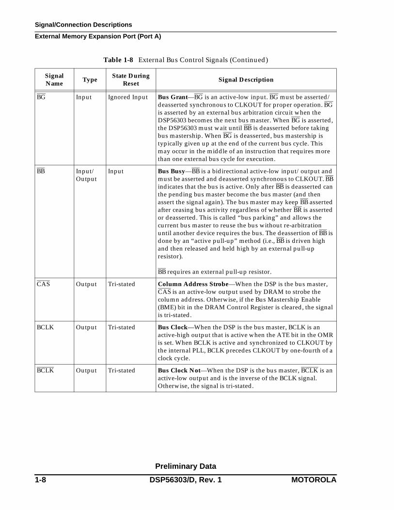
Preliminary Data
1-8 DSP56303/D, Rev. 1 MOTOROLA
Signal/Connection Descriptions
External Memory Expansion Port (Port A)
BG Input Ignored Input Bus Grant—BG is an active-low input. BG must be asserted/deasserted synchronous to CLKOUT for proper operation. BG is asserted by an external bus arbitration circuit when the DSP56303 becomes the next bus master. When BG is asserted, the DSP56303 must wait until BB is deasserted before taking bus mastership. When BG is deasserted, bus mastership is typically given up at the end of the current bus cycle. This may occur in the middle of an instruction that requires more than one external bus cycle for execution.
BB Input/Output
Input Bus Busy—BB is a bidirectional active-low input/output and must be asserted and deasserted synchronous to CLKOUT. BB indicates that the bus is active. Only after BB is deasserted can the pending bus master become the bus master (and then assert the signal again). The bus master may keep BB asserted after ceasing bus activity regardless of whether BR is asserted or deasserted. This is called “bus parking” and allows the current bus master to reuse the bus without re-arbitration until another device requires the bus. The deassertion of BB is done by an “active pull-up” method (i.e., BB is driven high and then released and held high by an external pull-up resistor).
BB requires an external pull-up resistor.
CAS Output Tri-stated Column Address Strobe—When the DSP is the bus master, CAS is an active-low output used by DRAM to strobe the column address. Otherwise, if the Bus Mastership Enable (BME) bit in the DRAM Control Register is cleared, the signal is tri-stated.
BCLK Output Tri-stated Bus Clock—When the DSP is the bus master, BCLK is an active-high output that is active when the ATE bit in the OMR is set. When BCLK is active and synchronized to CLKOUT by the internal PLL, BCLK precedes CLKOUT by one-fourth of a clock cycle.
BCLK Output Tri-stated Bus Clock Not—When the DSP is the bus master, BCLK is an active-low output and is the inverse of the BCLK signal. Otherwise, the signal is tri-stated.
Table 1-8 External Bus Control Signals (Continued)
Signal Name
TypeState During
ResetSignal Description

Signal/Connection Descriptions
Interrupt and Mode Control
Preliminary Data
MOTOROLA DSP56303/D, Rev. 1 1-9
INTERRUPT AND MODE CONTROL
The interrupt and mode control signals select the chip’s operating mode as it comes out of hardware reset. After RESET is deasserted, these inputs are hardware interrupt request lines.
Table 1-9 Interrupt and Mode Control
Signal Name TypeState During
ResetSignal Description
RESET Input Input Reset—RESET is an active-low, Schmitt-trigger input. Deassertion of RESET is internally synchronized to the clock out (CLKOUT). When asserted, the chip is placed in the Reset state and the internal phase generator is reset. The Schmitt-trigger input allows a slowly rising input (such as a capacitor charging) to reset the chip reliably. If RESET is deasserted synchronous to CLKOUT, exact start-up timing is guaranteed, allowing multiple processors to start synchronously and operate together in “lock-step.” When the RESET signal is deasserted, the initial chip operating mode is latched from the MODA, MODB, MODC, and MODD inputs. The RESET signal must be asserted after power up.
RESET can tolerate 5 V.
MODA/IRQA Input Input Mode Select A/External Interrupt Request A—MODA/IRQA is an active-low Schmitt-trigger input, internally synchronized to CLKOUT. MODA/IRQA selects the initial chip operating mode during hardware reset and becomes a level-sensitive or negative-edge-triggered, maskable interrupt request input during normal instruction processing. MODA, MODB, MODC, and MODD select one of sixteen initial chip operating modes, latched into the OMR when the RESET signal is deasserted. If IRQA is asserted synchronous to CLKOUT, multiple processors can be re-synchronized using the WAIT instruction and asserting IRQA to exit the Wait state. If the processor is in the Stop standby state and IRQA is asserted, the processor will exit the Stop state.
MODA/IRQA can tolerate 5 V.

Preliminary Data
1-10 DSP56303/D, Rev. 1 MOTOROLA
Signal/Connection Descriptions
Interrupt and Mode Control
MODB/IRQB Input Input Mode Select B/External Interrupt Request B—MODB/IRQB is an active-low Schmitt-trigger input, internally synchronized to CLKOUT. MODB/IRQB selects the initial chip operating mode during hardware reset and becomes a level-sensitive or negative-edge-triggered, maskable interrupt request input during normal instruction processing. MODA, MODB, MODC, and MODD select one of sixteen initial chip operating modes, latched into OMR when the RESET signal is deasserted. If IRQB is asserted synchronous to CLKOUT, multiple processors can be re-synchronized using the WAIT instruction and asserting IRQB to exit the Wait state.
MODB/IRQB can tolerate 5 V.
MODC/IRQC Input Input Mode Select C/External Interrupt Request C—MODC/IRQC is an active-low Schmitt-trigger input, internally synchronized to CLKOUT. MODC/IRQC selects the initial chip operating mode during hardware reset and becomes a level-sensitive or negative-edge-triggered, maskable interrupt request input during normal instruction processing. MODA, MODB, MODC, and MODD select one of sixteen initial chip operating modes, latched into OMR when the RESET signal is deasserted. If IRQC is asserted synchronous to CLKOUT, multiple processors can be re-synchronized using the WAIT instruction and asserting IRQC to exit the Wait state.
MODC/IRQC can tolerate 5 V.
MODD/IRQD Input Input Mode Select D/External Interrupt Request D—MODD/IRQD is an active-low Schmitt-trigger input, internally synchronized to CLKOUT. MODD/IRQD selects the initial chip operating mode during hardware reset and becomes a level-sensitive or negative-edge-triggered, maskable interrupt request input during normal instruction processing. MODA, MODB, MODC, and MODD select one of sixteen initial chip operating modes, latched into OMR when the RESET signal is deasserted. If IRQD is asserted synchronous to CLKOUT, multiple processors can be re-synchronized using the WAIT instruction and asserting IRQD to exit the Wait state.
MODD/IRQD can tolerate 5 V.
Table 1-9 Interrupt and Mode Control (Continued)
Signal Name TypeState During
ResetSignal Description

Signal/Connection Descriptions
Host Interface (HI08)
Preliminary Data
MOTOROLA DSP56303/D, Rev. 1 1-11
HOST INTERFACE (HI08)
The HI08 provides a fast parallel data to 8-bit port, which may be connected directly to the host bus.
The HI08 supports a variety of standard buses, and can be directly connected to a number of industry standard microcomputers, microprocessors, DSPs, and DMA hardware.
Host Port Usage Considerations
Careful synchronization is required when reading multiple-bit registers that are written by another asynchronous system. This is a common problem when two asynchronous systems are connected (as they are in the Host port). The considerations for proper operation are discussed in the following table:
Table 1-10 Host Port Usage Considerations
Action Description
Asynchronous read of receive byte registers
When reading the receive byte registers, Receive register High (RXH), Receive register Middle (RXM), or Receive register Low (RXL), the host interface programmer should use interrupts or poll the Receive register Data Full (RXDF) flag which indicates that data is available. This assures that the data in the receive byte registers will be valid.
Asynchronous write to transmit byte registers
The host interface programmer should not write to the transmit byte registers, Transmit register High (TXH), Transmit register Middle (TXM), or Transmit register Low (TXL), unless the Transmit register Data Empty (TXDE) bit is set indicating that the transmit byte registers are empty. This guarantees that the transmit byte registers will transfer valid data to the Host Receive (HRX) register.
Asynchronous write to host vector
The host interface programmer should change the Host Vector (HV) register only when the Host Command bit (HC) is clear. This will guarantee that the DSP interrupt control logic will receive a stable vector.

Preliminary Data
1-12 DSP56303/D, Rev. 1 MOTOROLA
Signal/Connection Descriptions
Host Interface (HI08)
Host Port Configuration
The functions of the signals associated with the HI08 vary according to the programmed configuration of the interface as determined by the 16 bits in the HI08 Port Control Register (HPCR). Refer to the DSP56303 User’s Manual for detailed descriptions of this and the other configuration registers used with the HI08.
Table 1-11 Host Interface
Signal Name TypeState During
ResetSignal Description
H0–H7
HAD0–HAD7
PB0–PB7
Input/Output
Input/Output
Input or Output
Tri-stated Host Data—When the HI08 is programmed to interface a non-multiplexed host bus and the HI function is selected, these signals are lines 0–7 of the Data bidirectional, tri-state bus.
Host Address—When HI08 is programmed to interface a multiplexed host bus and the HI function is selected, these signals are lines 0–7 of the Address/Data bidirectional, multiplexed, tri-state bus.
Port B 0–7—When the HI08 is configured as GPIO through the HPCR, these signals are individually programmed as inputs or outputs through the HI08 Data Direction Register (HDDR).
This input is 5 V tolerant.
HA0
HAS/HAS
PB8
Input
Input
Input or Output
Input Host Address Input 0—When the HI08 is programmed to interface a non-multiplexed host bus and the HI function is selected, this signal is line 0 of the Host Address input bus.
Host Address Strobe—When HI08 is programmed to interface a multiplexed host bus and the HI function is selected, this signal is the Host Address Strobe (HAS) Schmitt-trigger input. The polarity of the address strobe is programmable but is configured active-low (HAS) following reset.
Port B 8—When the HI08 is configured as GPIO through the HPCR, this signal is individually programmed as an input or output through the HDDR.
This input is 5 V tolerant.

Signal/Connection Descriptions
Host Interface (HI08)
Preliminary Data
MOTOROLA DSP56303/D, Rev. 1 1-13
HA1
HA8
PB9
Input
Input
Input or Output
Input Host Address Input 1—When the HI08 is programmed to interface a non-multiplexed host bus and the HI function is selected, this signal is line 1 of the Host Address (HA1) input bus.
Host Address 8—When HI08 is programmed to interface a multiplexed host bus and the HI function is selected, this signal is line 8 of the Host Address (HA8) input bus.
Port B 9—When the HI08 is configured as GPIO through the HPCR, this signal is individually programmed as an input or output through the HDDR.
This input is 5 V tolerant.
HA2
HA9
PB10
Input
Input
Input or Output
Input Host Address Input 2—When the HI08 is programmed to interface a non-multiplexed host bus and the HI function is selected, this signal is line 2 of the Host Address (HA2) input bus.
Host Address 9—When HI08 is programmed to interface a multiplexed host bus and the HI function is selected, this signal is line 9 of the Host Address (HA9) input bus.
Port B 10—When the HI08 is configured as GPIO through the HPCR, this signal is individually programmed as an input or output through the HDDR.
This input is 5 V tolerant.
HRW
HRD/HRD
PB11
Input
Input
Input or Output
Input Host Read/Write—When HI08 is programmed to interface a single-data-strobe host bus and the HI function is selected, this signal is the Host Read/Write (HRW) input.
Host Read Data—When HI08 is programmed to interface a double-data-strobe host bus and the HI function is selected, this signal is the Host Read Data strobe (HRD) Schmitt-trigger input. The polarity of the data strobe is programmable, but is configured as active-low (HRD) after reset.
Port B 11—When the HI08 is configured as GPIO through the HPCR, this signal is individually programmed as an input or output through the HDDR.
This input is 5 V tolerant.
Table 1-11 Host Interface (Continued)
Signal Name TypeState During
ResetSignal Description

Preliminary Data
1-14 DSP56303/D, Rev. 1 MOTOROLA
Signal/Connection Descriptions
Host Interface (HI08)
HDS/HDS
HWR/HWR
PB12
Input
Input
Input or Output
Input Host Data Strobe—When HI08 is programmed to interface a single-data-strobe host bus and the HI function is selected, this signal is the Host Data Strobe (HDS) Schmitt-trigger input. The polarity of the data strobe is programmable, but is configured as active-low (HDS) following reset.
Host Write Data—When HI08 is programmed to interface a double-data-strobe host bus and the HI function is selected, this signal is the Host Write Data Strobe (HWR) Schmitt-trigger input. The polarity of the data strobe is programmable, but is configured as active-low (HWR) following reset.
Port B 12—When the HI08 is configured as GPIO through the HPCR, this signal is individually programmed as an input or output through the HDDR.
This input is 5 V tolerant.
HCS
HA10
PB13
Input
Input
Input or Output
Input Host Chip Select—When HI08 is programmed to interface a non-multiplexed host bus and the HI function is selected, this signal is the Host Chip Select (HCS) input. The polarity of the chip select is programmable, but is configured active-low (HCS) after reset.
Host Address 10—When HI08 is programmed to interface a multiplexed host bus and the HI function is selected, this signal is line 10 of the Host Address (HA10) input bus.
Port B 13—When the HI08 is configured as GPIO through the HPCR, this signal is individually programmed as an input or output through the HDDR.
This input is 5 V tolerant.
Table 1-11 Host Interface (Continued)
Signal Name TypeState During
ResetSignal Description

Signal/Connection Descriptions
Host Interface (HI08)
Preliminary Data
MOTOROLA DSP56303/D, Rev. 1 1-15
HREQ/HREQ
HTRQ/HTRQ
PB14
Output
Output
Input or Output
Input Host Request—When HI08 is programmed to interface a single host request host bus and the HI function is selected, this signal is the Host Request (HREQ) output. The polarity of the host request is programmable, but is configured as active-low (HREQ) following reset. The host request may be programmed as a driven or open-drain output.
Transmit Host Request—When HI08 is programmed to interface a double host request host bus and the HI function is selected, this signal is the Transmit Host Request (HTRQ) output. The polarity of the host request is programmable, but is configured as active-low (HTRQ) following reset. The host request may be programmed as a driven or open-drain output.
Port B 14—When the HI08 is programmed to interface a multiplexed host bus and the signal is configured as GPIO through the HPCR, this signal is individually programmed as an input or output through the HDDR.
This input is 5 V tolerant.
HACK/HACK
HRRQ/HRRQ
PB15
Input
Output
Input or Output
Input Host Acknowledge—When HI08 is programmed to interface a single host request host bus and the HI function is selected, this signal is the Host Acknowledge (HACK) Schmitt-trigger input. The polarity of the host acknowledge is programmable, but is configured as active-low (HACK) after reset.
Receive Host Request—When HI08 is programmed to interface a double host request host bus and the HI function is selected, this signal is the Receive Host Request (HRRQ) output. The polarity of the host request is programmable, but is configured as active-low (HRRQ) after reset. The host request may be programmed as a driven or open-drain output.
Port B 15—When the HI08 is configured as GPIO through the HPCR, this signal is individually programmed as an input or output through the HDDR.
This input is 5 V tolerant.
Table 1-11 Host Interface (Continued)
Signal Name TypeState During
ResetSignal Description

Preliminary Data
1-16 DSP56303/D, Rev. 1 MOTOROLA
Signal/Connection Descriptions
Enhanced Synchronous Serial Interface 0 (ESSI0)
ENHANCED SYNCHRONOUS SERIAL INTERFACE 0 (ESSI0)
There are two synchronous serial interfaces (ESSI0 and ESSI1) that provide a full-duplex serial port for serial communication with a variety of serial devices, including one or more industry-standard codecs, other DSPs, microprocessors, and peripherals which implement the Motorola Serial Peripheral Interface (SPI).
Table 1-12 Enhanced Synchronous Serial Interface 0 (ESSI0)
Signal Name TypeState During
ResetSignal Description
SC00
PC0
Input or Output
Input Serial Control 0—The function of SC00 is determined by the selection of either Synchronous or Asynchronous mode. For Asynchronous mode, this signal will be used for the receive clock I/O (Schmitt-trigger input). For Synchronous mode, this signal is used either for Transmitter 1 output or for Serial I/O Flag 0.
Port C 0—The default configuration following reset is GPIO input PC0. When configured as PC0, signal direction is controlled through the Port Directions Register (PRR0). The signal can be configured as ESSI signal SC00 through the Port Control Register (PCR0).
This input is 5 V tolerant.
SC01
PC1
Input/Output
Input or Output
Input Serial Control 1—The function of this signal is determined by the selection of either Synchronous or Asynchronous mode. For Asynchronous mode, this signal is the receiver frame sync I/O. For Synchronous mode, this signal is used either for Transmitter 2 output or for Serial I/O Flag 1.
Port C 1—The default configuration following reset is GPIO input PC1. When configured as PC1, signal direction is controlled through PRR0. The signal can be configured as an ESSI signal SC01 through PCR0.
This input is 5 V tolerant.

Signal/Connection Descriptions
Enhanced Synchronous Serial Interface 0 (ESSI0)
Preliminary Data
MOTOROLA DSP56303/D, Rev. 1 1-17
SC02
PC2
Input/Output
Input or Output
Input Serial Control Signal 2—SC02 is used for frame sync I/O. SC02 is the frame sync for both the transmitter and receiver in Synchronous mode, and for the transmitter only in Asynchronous mode. When configured as an output, this signal is the internally generated frame sync signal. When configured as an input, this signal receives an external frame sync signal for the transmitter (and the receiver in synchronous operation).
Port C 2—The default configuration following reset is GPIO input PC2. When configured as PC2, signal direction is controlled through PRR0. The signal can be configured as an ESSI signal SC02 through PCR0.
This input is 5 V tolerant.
SCK0
PC3
Input/Output
Input or Output
Input Serial Clock—SCK0 is a bidirectional Schmitt-trigger input signal providing the serial bit rate clock for the ESSI interface. The SCK0 is a clock input or output used by both the transmitter and receiver in Synchronous modes, or by the transmitter in Asynchronous modes.
Although an external serial clock can be independent of and asynchronous to the DSP system clock, it must exceed the minimum clock cycle time of 6 T (i.e., the system clock frequency must be at least three times the external ESSI clock frequency). The ESSI needs at least three DSP phases inside each half of the serial clock.
Port C 3—The default configuration following reset is GPIO input PC3. When configured as PC3, signal direction is controlled through PRR0. The signal can be configured as an ESSI signal SCK0 through PCR0.
This input is 5 V tolerant.
Table 1-12 Enhanced Synchronous Serial Interface 0 (ESSI0) (Continued)
Signal Name TypeState During
ResetSignal Description

Preliminary Data
1-18 DSP56303/D, Rev. 1 MOTOROLA
Signal/Connection Descriptions
Enhanced Synchronous Serial Interface 0 (ESSI0)
SRD0
PC4
Input/Output
Input or Output
Input Serial Receive Data—SRD0 receives serial data and transfers the data to the ESSI receive shift register. SRD0 is an input when data is being received.
Port C 4—The default configuration following reset is GPIO input PC4. When configured as PC4, signal direction is controlled through PRR0. The signal can be configured as an ESSI signal SRD0 through PCR0.
This input is 5 V tolerant.
STD0
PC5
Input/Output
Input or Output
Input Serial Transmit Data—STD0 is used for transmitting data from the serial transmit shift register. STD0 is an output when data is being transmitted.
Port C 5—The default configuration following reset is GPIO input PC5. When configured as PC5, signal direction is controlled through PRR0. The signal can be configured as an ESSI signal STD0 through PCR0.
This input is 5 V tolerant.
Table 1-12 Enhanced Synchronous Serial Interface 0 (ESSI0) (Continued)
Signal Name TypeState During
ResetSignal Description

Signal/Connection Descriptions
Enhanced Synchronous Serial Interface 1 (ESSI1)
Preliminary Data
MOTOROLA DSP56303/D, Rev. 1 1-19
ENHANCED SYNCHRONOUS SERIAL INTERFACE 1 (ESSI1)
Table 1-13 Enhanced Synchronous Serial Interface 1 (ESSI1)
Signal Name TypeState During
ResetSignal Description
SC10
PD0
Input or Output
Input Serial Control 0—The function of SC10 is determined by the selection of either Synchronous or Asynchronous mode. For Asynchronous mode, this signal will be used for the receive clock I/O (Schmitt-trigger input). For Synchronous mode, this signal is used either for Transmitter 1 output or for Serial I/O Flag 0.
Port D 0—The default configuration following reset is GPIO input PD0. When configured as PD0, signal direction is controlled through the Port Directions Register (PRR1). The signal can be configured as an ESSI signal SC10 through the Port Control Register (PCR1).
This input is 5 V tolerant.
SC11
PD1
Input/Output
Input or Output
Input Serial Control 1—The function of this signal is determined by the selection of either Synchronous or Asynchronous mode. For Asynchronous mode, this signal is the receiver frame sync I/O. For Synchronous mode, this signal is used either for Transmitter 2 output or for Serial I/O Flag 1.
Port D 1—The default configuration following reset is GPIO input PD1. When configured as PD1, signal direction is controlled through PRR1. The signal can be configured as an ESSI signal SC11 through PCR1.
This input is 5 V tolerant.

Preliminary Data
1-20 DSP56303/D, Rev. 1 MOTOROLA
Signal/Connection Descriptions
Enhanced Synchronous Serial Interface 1 (ESSI1)
SC12
PD2
Input/Output
Input or Output
Input Serial Control Signal 2—SC12 is used for frame sync I/O. SC12 is the frame sync for both the transmitter and receiver in Synchronous mode, and for the transmitter only in Asynchronous mode. When configured as an output, this signal is the internally generated frame sync signal. When configured as an input, this signal receives an external frame sync signal for the transmitter (and the receiver in Synchronous operation).
Port D 2—The default configuration following reset is GPIO input PD2. When configured as PD2, signal direction is controlled through PRR1. The signal can be configured as an ESSI signal SC12 through PCR1.
This input is 5 V tolerant.
SCK1
PD3
Input/Output
Input or Output
Input Serial Clock—SCK1 is a bidirectional Schmitt-trigger input signal providing the serial bit rate clock for the ESSI interface. The SCK1 is a clock input or output used by both the transmitter and receiver in Synchronous modes, or by the transmitter in Asynchronous modes.
Although an external serial clock can be independent of and asynchronous to the DSP system clock, it must exceed the minimum clock cycle time of 6T (i.e., the system clock frequency must be at least three times the external ESSI clock frequency). The ESSI needs at least three DSP phases inside each half of the serial clock.
Port D 3—The default configuration following reset is GPIO input PD3. When configured as PD3, signal direction is controlled through PRR1. The signal can be configured as an ESSI signal SCK1 through PCR1.
This input is 5 V tolerant.
Table 1-13 Enhanced Synchronous Serial Interface 1 (ESSI1) (Continued)
Signal Name TypeState During
ResetSignal Description

Signal/Connection Descriptions
Enhanced Synchronous Serial Interface 1 (ESSI1)
Preliminary Data
MOTOROLA DSP56303/D, Rev. 1 1-21
SRD1
PD4
Input/Output
Input or Output
Input Serial Receive Data—SRD1 receives serial data and transfers the data to the ESSI receive shift register. SRD1 is an input when data is being received.
Port D 4—The default configuration following reset is GPIO input PD4. When configured as PD4, signal direction is controlled through PRR1. The signal can be configured as an ESSI signal SRD1 through PCR1.
This input is 5 V tolerant.
STD1
PD5
Input/Output
Input or Output
Input Serial Transmit Data—STD1 is used for transmitting data from the serial transmit shift register. STD1 is an output when data is being transmitted.
Port D 5—The default configuration following reset is GPIO input PD5. When configured as PD5, signal direction is controlled through PRR1. The signal can be configured as an ESSI signal STD1 through PCR1.
This input is 5 V tolerant.
Table 1-13 Enhanced Synchronous Serial Interface 1 (ESSI1) (Continued)
Signal Name TypeState During
ResetSignal Description

Preliminary Data
1-22 DSP56303/D, Rev. 1 MOTOROLA
Signal/Connection Descriptions
Serial Communication Interface (SCI)
SERIAL COMMUNICATION INTERFACE (SCI)
The Serial Communication interface (SCI) provides a full duplex port for serial communication to otherDSPs, microprocessors, or peripherals such as modems.
Table 1-14 Serial Communication Interface (SCI)
Signal Name TypeState During
ResetSignal Description
RXD
PE0
Input
Input or Output
Input Serial Receive Data—This input receives byte oriented serial data and transfers it to the SCI receive shift register.
Port E 0—The default configuration following reset is GPIO input PE0. When configured as PE0, signal direction is controlled through the SCI Port Directions Register (PRR). The signal can be configured as an SCI signal RXD through the SCI Port Control Register (PCR).
This input is 5 V tolerant.
TXD
PE1
Output
Input or Output
Input Serial Transmit Data—This signal transmits data from SCI transmit data register.
Port E 1—The default configuration following reset is GPIO input PE1. When configured as PE1, signal direction is controlled through the SCI PRR. The signal can be configured as an SCI signal TXD through the SCI PCR.
This input is 5 V tolerant.
SCLK
PE2
Input/Output
Input or Output
Input Serial Clock—This is the bidirectional Schmitt-trigger input signal providing the input or output clock used by the transmitter and/or the receiver.
Port E 2—The default configuration following reset is GPIO input PE2. When configured as PE2, signal direction is controlled through the SCI PRR. The signal can be configured as an SCI signal SCLK through the SCI PCR.
This input is 5 V tolerant.
Signal/Connection Descriptions
TimerS
Preliminary Data
MOTOROLA DSP56303/D, Rev. 1 1-23
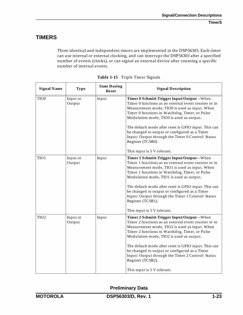
TIMERS
Three identical and independent timers are implemented in the DSP56303. Each timer can use internal or external clocking, and can interrupt the DSP56303 after a specified number of events (clocks), or can signal an external device after counting a specific number of internal events.
Table 1-15 Triple Timer Signals
Signal Name TypeState During
ResetSignal Description
TIO0 Input or Output
Input Timer 0 Schmitt-Trigger Input/Output—When Timer 0 functions as an external event counter or in Measurement mode, TIO0 is used as input. When Timer 0 functions in Watchdog, Timer, or Pulse Modulation mode, TIO0 is used as output.
The default mode after reset is GPIO input. This can be changed to output or configured as a Timer Input/Output through the Timer 0 Control/Status Register (TCSR0).
This input is 5 V tolerant.
TIO1 Input or Output
Input Timer 1 Schmitt-Trigger Input/Output—When Timer 1 functions as an external event counter or in Measurement mode, TIO1 is used as input. When Timer 1 functions in Watchdog, Timer, or Pulse Modulation mode, TIO1 is used as output.
The default mode after reset is GPIO input. This can be changed to output or configured as a Timer Input/Output through the Timer 1 Control/Status Register (TCSR1).
This input is 5 V tolerant.
TIO2 Input or Output
Input Timer 2 Schmitt-Trigger Input/Output—When Timer 2 functions as an external event counter or in Measurement mode, TIO2 is used as input. When Timer 2 functions in Watchdog, Timer, or Pulse Modulation mode, TIO2 is used as output.
The default mode after reset is GPIO input. This can be changed to output or configured as a Timer Input/Output through the Timer 2 Control/Status Register (TCSR2).
This input is 5 V tolerant.

Preliminary Data
1-24 DSP56303/D, Rev. 1 MOTOROLA
Signal/Connection Descriptions
JTAG/OnCE Interface
JTAG/ONCE INTERFACE
Table 1-16 JTAG/OnCE Interface
Signal Name TypeState During
ResetSignal Description
TCK Input Input Test Clock—TCK is a test clock input signal used to synchronize the JTAG test logic.
This input is 5 V tolerant.
TDI Input Input Test Data Input—TDI is a test data serial input signal used for test instructions and data. TDI is sampled on the rising edge of TCK and has an internal pull-up resistor.
This input is 5 V tolerant.
TDO Output Tri-stated Test Data Output—TDO is a test data serial output signal used for test instructions and data. TDO is tri-statable and is actively driven in the shift-IR and shift-DR controller states. TDO changes on the falling edge of TCK.
TMS Input Input Test Mode Select—TMS is an input signal used to sequence the test controller’s state machine. TMS is sampled on the rising edge of TCK and has an internal pull-up resistor.
This input is 5 V tolerant.
TRST Input Input Test Reset—TRST is an active-low Schmitt-trigger input signal used to asynchronously initialize the test controller. TRST has an internal pull-up resistor. TRST must be asserted after power up.
This input is 5 V tolerant.

Signal/Connection Descriptions
JTAG/OnCE Interface
Preliminary Data
MOTOROLA DSP56303/D, Rev. 1 1-25
DE Input/Output Input Debug Event—DE is an open-drain, bidirectional, active-low signal providing, as an input, a means of entering the Debug mode of operation from an external command controller, and, as an output, a means of acknowledging that the chip has entered the Debug mode. This signal, when asserted as an input, causes the DSP56300 core to finish the current instruction being executed, save the instruction pipeline information, enter the Debug mode, and wait for commands to be entered from the debug serial input line. This signal is asserted as an output for three clock cycles when the chip enters the Debug mode as a result of a debug request or as a result of meeting a breakpoint condition. The DE has an internal pull-up resistor.
This is not a standard part of the JTAG Test Access Port (TAP) Controller. The signal connects directly to the OnCE module to initiate Debug mode directly or to provide a direct external indication that the chip has entered the Debug mode. All other interface with the OnCE module must occur through the JTAG port.
This input is 5 V tolerant.
Table 1-16 JTAG/OnCE Interface (Continued)
Signal Name TypeState During
ResetSignal Description

Preliminary Data
1-26 DSP56303/D, Rev. 1 MOTOROLA
Signal/Connection Descriptions
JTAG/OnCE Interface

Preliminary Data
MOTOROLA DSP56303/D, Rev. 1 2-1
SECTION 2
SPECIFICATIONS
INTRODUCTION
The DSP56303 is fabricated in high density CMOS with Transistor-Transistor Logic (TTL) compatible inputs and outputs. The DSP56303 specifications are preliminary and are from design simulations, and may not be fully tested or guaranteed at this early stage of the product life cycle. Finalized specifications will be published after full characterization and device qualifications are complete.
MAXIMUM RATINGS
Note: In the calculation of timing requirements, adding a maximum value of one specification to a minimum value of another specification does not yield a reasonable sum. A maximum specification is calculated using a worst case variation of process parameter values in one direction. The minimum specification is calculated using the worst case for the same parameters in the opposite direction. Therefore, a “maximum” value for a specification will never occur in the same device that has a “minimum” value for another specification; adding a maximum to a minimum represents a condition that can never exist.
CAUTION
This device contains circuitry protectingagainst damage due to high static voltage orelectrical fields; however, normal precautionsshould be taken to avoid exceeding maximumvoltage ratings. Reliability is enhanced ifunused inputs are tied to an appropriate logicvoltage level (e.g., either GND or VCC).

Preliminary Data
2-2 DSP56303/D, Rev. 1 MOTOROLA
Specifications
Thermal Characteristics
THERMAL CHARACTERISTICS
Table 2-1 Maximum Ratings
Rating1 Symbol Value1, 2 Unit
Supply Voltage VCC −0.3 to +4.0 V
All input voltages excluding “5 V tolerant” inputs3 VIN GND − 0.3 to VCC + 0.3 V
All “5 V tolerant” input voltages3 VIN5 GND − 0.3 to VCC + 3.95 V
Current drain per pin excluding VCC and GND I 10 mA
Operating temperature range TJ −40 to +100 °C
Storage temperature TSTG −55 to +150 °C
Notes: 1. GND = 0 V, VCC = 3.3 V ± 0.3 V, TJ = –40°C to +100°C, CL = 50 pF + 2 TTL Loads2. Absolute maximum ratings are stress ratings only, and functional operation at the maximum is not
guaranteed. Stress beyond the maximum rating may affect device reliability or cause permanent damage to the device.
3. CAUTION: All “5 V Tolerant” input voltages cannot be more than 3.95 V greater than the supply voltage; this restriction applies to “power on”, as well as during normal operation. In any case, the input voltages can not be more than 5.75 V. “5 V Tolerant” inputs are inputs that tolerate 5 V.
Table 2-2 Thermal Characteristics
Characteristic SymbolTQFP Value
PBGA3 Value
PBGA4 Value
Unit
Junction-to-ambient thermal resistance RθJA or θJA 55.7 57 28 °C/W
Junction-to-case thermal resistance RθJC or θJC 11.4 15 — °C/W
Thermal characterization parameter ΨJT 6.8 8 — °C/W
Notes: 1. Junction-to-ambient thermal resistance is based on measurements on a horizontal single-sided printed circuit board per SEMI G38-87 in natural convection.(SEMI is Semiconductor Equipment and Materials International, 805 East Middlefield Rd., Mountain View, CA 94043, (415) 964-5111)
2. Junction-to-case thermal resistance is based on measurements using a cold plate per SEMI G30-88, with the exception that the cold plate temperature is used for the case temperature.
3. These are simulated values; testing is not complete. See note 1 for test board conditions.4. These are simulated values; testing is not complete. The test board has two, 2-ounce signal layers and
two 1-ounce solid ground planes internal to the test board.

Specifications
DC Electrical Characteristics
Preliminary Data
MOTOROLA DSP56303/D, Rev. 1 2-3
DC ELECTRICAL CHARACTERISTICS
Table 2-3 DC Electrical Characteristics6
Characteristics Symbol Min Typ Max Unit
Supply voltage VCC 3.0 3.3 3.6 V
Input high voltage• D(0:23), BG, BB, TA• MOD1/IRQ1, RESET, PINIT/NMI
and all JTAG/ESSI/SCI/Timer/HI08 pins
• EXTAL8
VIHVIHP
VIHX
2.02.0
0.8 × VCC
——
—
VCCVCC + 3.95
VCC
VV
V
Input low voltage• D(0:23), BG, BB, TA, MOD1/IRQ1,
RESET, PINIT• All JTAG/ESSI/SCI/Timer/HI08
pins• EXTAL8
VIL
VILP
VILX
–0.3
–0.3
–0.3
—
—
—
0.8
0.8
0.2 × VCC
V
V
V
Input leakage current IIN –10 — 10 µA
High impedance (off-state) input current (@ 2.4 V / 0.4 V)
ITSI –10 — 10 µA
Output high voltage • TTL (IOH = –0.4 mA)5,7
• CMOS (IOH = –10 µA)5
VOHVCC – 0.4VCC – 0.01
——
——
VV
Output low voltage • TTL (IOL = 3.0 mA, open-drain pins
IOL = 6.7 mA)5,7
• CMOS (IOL = 10 µA)5
VOL—
—
—
—
0.4
0.01
V
V
Internal supply current2:• In Normal mode
• In Wait mode3
• In Stop mode4
ICCI
ICCW
ICCS
—
—
—
66 MHz: 8480 MHz: 102100 MHz: 12766 MHz: 580 MHz: 6100 MHz: 7. 566 MHz: 10080 MHz: 100100 MHz: 100
66 MHz: 12080 MHz: 145100 MHz: 18166 MHz: 780 MHz: 9100 MHz: 1166 MHz: 15080 MHz: 150100 MHz: 150
mAmAmAmAmAmAµAµAµA
PLL supply current in Stop mode5 — 1 2.5 mA
Input capacitance5 CIN — — 10 pF

Preliminary Data
2-4 DSP56303/D, Rev. 1 MOTOROLA
Specifications
AC Electrical Characteristics
AC ELECTRICAL CHARACTERISTICS
The timing waveforms shown in the AC electrical characteristics section are tested with a VIL maximum of 0.3 V and a VIH minimum of 2.4 V for all pins except EXTAL, which is tested using the input levels shown in Note 6 of the previous table. AC timing specifications, which are referenced to a device input signal, are measured in production with respect to the 50% point of the respective input signal’s transition. DSP56303 output levels are measured with the production test machine VOL and VOH reference levels set at 0.8 V and 2.0 V, respectively.
Notes: 1. Refers to MODA/IRQA, MODB/IRQB, MODC/IRQC, and MODD/IRQD pins2. Power Consumption Considerations on page 4-4 provides a formula to compute the
estimated current requirements in Normal mode. In order to obtain these results, all inputs must be terminated (i.e., not allowed to float). Measurements are based on synthetic intensive DSP benchmarks (see Appendix A). The power consumption numbers in this specification are 90% of the measured results of this benchmark. This reflects typical DSP applications. Typical internal supply current is measured with VCC = 3.0 V at TJ = 100°C. Maximum internal supply current is measured with VCC = 3.6 V at TJ = 100°C.
3. In order to obtain these results, all inputs must be terminated (i.e., not allowed to float). PLL and XTAL signals are disabled during Stop state.
4. In order to obtain these results, all inputs, which are not disconnected at Stop mode, must be terminated (i.e., not allowed to float).
5. Periodically sampled and not 100% tested 6. VCC = 3.3 V ± 0.3 V; TJ = –40°C to +100 °C, CL = 50 pF + 2 TTL Loads7. This characteristic does not apply to XTAL and PCAP.8. Driving EXTAL to the low VIHX or the high VILX value may cause additional power consumption (DC
current). To minimize power consumption, the minimum VIHX should be no lower than 0.9 × VCC and the maximum VILX should be no higher than 0.1 × VCC.
Table 2-3 DC Electrical Characteristics6 (Continued)
Characteristics Symbol Min Typ Max Unit

Specifications
Internal Clocks
Preliminary Data
MOTOROLA DSP56303/D, Rev. 1 2-5
INTERNAL CLOCKS
Table 2-4 Internal Clocks, CLKOUT
Characteristics SymbolExpression1, 2
Min Typ Max
Internal operation frequency and CLKOUT with PLL enabled
f — (Ef × MF)/(PDF × DF)
—
Internal operation frequency and CLKOUT with PLL disabled
f — Ef/2 —
Internal clock and CLKOUT high period• With PLL disabled• With PLL enabled and
MF ≤ 4• With PLL enabled and
MF > 4
TH —0.49 × ETC ×
PDF × DF/MF0.47 × ETC ×
PDF × DF/MF
ETC—
—
—0.51 × ETC ×
PDF × DF/MF0.53 × ETC ×
PDF × DF/MF
Internal clock and CLKOUT low period• With PLL disabled• With PLL enabled and
MF ≤ 4• With PLL enabled and
MF > 4
TL —0.49 × ETC ×
PDF × DF/MF0.47 × ETC ×
PDF × DF/MF
ETC—
—
—0.51 × ETC ×
PDF × DF/MF0.53 × ETC ×
PDF × DF/MF
Internal clock and CLKOUT cycle time with PLL enabled
TC — ETC × PDF × DF/MF
—
Internal clock and CLKOUT cycle time with PLL disabled
TC — 2 × ETC —
Instruction cycle time ICYC — TC —
Notes: 1. DF = Division FactorEf = External frequencyETC = External clock cycleMF = Multiplication FactorPDF = Predivision FactorTC = internal clock cycle
2. See the PLL and Clock Generation section in the DSP56300 Family Manual for a detailed discussion of the PLL.

Preliminary Data
2-6 DSP56303/D, Rev. 1 MOTOROLA
Specifications
EXTERNAL CLOCK OPERATION
EXTERNAL CLOCK OPERATION
The DSP56303 system clock may be derived from the on−chip crystal oscillator, as shown in Figure 1 on the cover page, or it may be externally supplied. An externally supplied square wave voltage source should be connected to EXTAL (see Figure 2-2), leaving XTAL physically not connected to the board or socket.
Figure 2-1 Crystal Oscillator Circuits
Suggested Component Values:fOSC = 4 MHzR = 680 kΩ ± 10%C = 56 pF ± 20%
Calculations were done for a 4/20 MHz crystal with the following parameters: a CLof 30/20 pF, a C0 of 7/6 pF, a series resistance of 100/20 Ω, anda drive level of 2 mW.
Suggested Component Values:fOSC = 32.768 kHzR1 = 3.9 MΩ ± 10%C = 22 pF ± 20%R2 = 200 kΩ ± 10%
Calculations were done for a 32.768 kHz crystal with the following parameters: a load capacitance (CL) of 12.5 pF, a shunt capacitance (C0) of 1.8 pF, a series resistance of 40 kΩ, and a drive level of 1 µW.
XTAL1C C
R1
Fundamental FrequencyFork Crystal Oscillator
XTALEXTAL
XTAL1C C
R
Fundamental FrequencyCrystal Oscillator
XTALEXTAL
R2
fOSC = 20 MHzR = 680 kΩ ± 10%C = 22 pF ± 20%
AA1071

Specifications
EXTERNAL CLOCK OPERATION
Preliminary Data
MOTOROLA DSP56303/D, Rev. 1 2-7
Figure 2-2 External Clock Timing
Table 2-5 Clock Operation
No. Characteristics Symbol66 MHz 80 MHz 100 MHz
Min Max Min Max Min Max
1 Frequency of EXTAL (EXTAL Pin Frequency)The rise and fall time of this external clock should be 3 ns maximum.
Ef 0 66.0 0 80.0 0 100.0
2 EXTAL input high1, 2
• With PLL disabled (46.7%–53.3% duty cycle6)
• With PLL enabled (42.5%–57.5% duty cycle6)
ETH 7.08 ns
6.44 ns
∞
157.0 µs
5.84 ns
5.31 ns
∞
157.0 µs
4.67 ns
4.25 ns
∞
157.0 µs
3 EXTAL input low1, 2
• With PLL disabled (46.7%–53.3% duty cycle6)
• With PLL enabled (42.5%–57.5% duty cycle6)
ETL 7.08 ns
6.44 ns
∞
157.0 µs
5.84 ns
5.31 ns
∞
157.0 µs
4.67 ns
4.25 ns
∞
157.0 µs
EXTAL
VILC
VIHC
Midpoint
Note: The midpoint is 0.5 (VIHC + VILC).
ETH ETL
ETC
CLKOUT WithPLL Disabled
CLKOUT WithPLL Enabled
7
5
7
6b
5
3
4
2
AA0459
6a

Preliminary Data
2-8 DSP56303/D, Rev. 1 MOTOROLA
Specifications
EXTERNAL CLOCK OPERATION
4 EXTAL cycle time2
• With PLL disabled• With PLL enabled
ETC 15.15 ns15.15 ns
∞273.1 µs
12.50 ns12.50 ns
∞273.1 µs
10.00 ns10.00 ns
∞273.1 µs
5 CLKOUT change from EXTAL fall with PLL disabled
4.3 ns 11.0 ns 4.3 ns 11.0 ns 4.3 ns 11.0 ns
6 CLKOUT rising edge from EXTAL rising edge with PLL enabled (MF = 1, PDF = 1, Ef > 15 MHz)3,5
CLKOUT falling edge from EXTAL rising edge with PLL enabled (MF = 2 or 4, PDF = 1, Ef > 15 MHz)3,5
CLKOUT falling edge from EXTAL falling edge with PLL enabled (MF ≤ 4, PDF ≠ 1, Ef / PDF > 15 MHz)3,5
0.0 ns
0.0 ns
0.0 ns
1.8 ns
1.8 ns
1.8 ns
0.0 ns
0.0 ns
0.0 ns
1.8 ns
1.8 ns
1.8 ns
0.0 ns
0.0 ns
0.0 ns
1.8 ns
1.8 ns
1.8 ns
7 Instruction cycle time = ICYC = TC
4
(see Table 2-4) (46.7%–53.3% duty cycle)• With PLL disabled• With PLL enabled
ICYC
30.3 ns15.15 ns
∞8.53 µs
25.0 ns12.50 ns
∞8.53 µs
20.0 ns10.00 ns
∞8.53 µs
Notes: 1. Measured at 50% of the input transition2. The maximum value for PLL enabled is given for minimum VCO and maximum MF.3. Periodically sampled and not 100% tested4. The maximum value for PLL enabled is given for minimum VCO and maximum DF.5. The skew is not guaranteed for any other MF value.6. The indicated duty cycle is for the specified maximum frequency for which a part is rated. The
minimum clock high or low time required for correction operation, however, remains the same at lower operating frequencies; therefore, when a lower clock frequency is used, the signal symmetry may vary from the specified duty cycle as long as the minimum high time and low time requirements are met.
Table 2-5 Clock Operation (Continued)
No. Characteristics Symbol66 MHz 80 MHz 100 MHz
Min Max Min Max Min Max

Specifications
Phase Lock Loop (PLL) Characteristics
Preliminary Data
MOTOROLA DSP56303/D, Rev. 1 2-9
PHASE LOCK LOOP (PLL) CHARACTERISTICS
Table 2-6 PLL Characteristics
Characteristics66 MHz 80 MHz 100 MHz
UnitMin Max Min Max Min Max
VCO frequency when PLL enabled (MF × Ef × 2/PDF)
30 132 30 160 30 200 MHz
PLL external capacitor (PCAP pin to VCCP) (CPCAP
1)
• @ MF ≤ 4
• @ MF > 4
(MF × 425) − 125
MF × 520
(MF × 590) − 175
MF × 920
(MF × 425) − 125
MF × 520
(MF × 590) − 175
MF × 920
(MF × 425) − 125
MF × 520
(MF × 590) − 175
MF × 920
pF
pF
Note: CPCAP is the value of the PLL capacitor (connected between the PCAP pin and VCCP). The recommended value in pF for CPCAP can be computed from one of the following equations:
(500 × MF) – 150, for MF ≤ 4, or690 × MF, for MF > 4.

Preliminary Data
2-10 DSP56303/D, Rev. 1 MOTOROLA
Specifications
Reset, Stop, Mode Select, and Interrupt Timing
RESET, STOP, MODE SELECT, AND INTERRUPT TIMING
Table 2-7 Reset, Stop, Mode Select, and Interrupt Timing6
No. Characteristics Expression 66 MHz 80 MHz 100 MHz
UnitMin Max Min Max Min Max
8 Delay from RESET assertion to all pins at reset value3
— — 26.0 — 26.0 — 26.0 ns
9 Required RESET duration4
• Power on, external clock generator, PLL disabled
• Power on, external clock generator, PLL enabled
• Power on, internal oscillator
• During STOP, XTAL disabled (PCTL Bit 16 = 0)
• During STOP, XTAL enabled (PCTL Bit 16 = 1)
• During normal operation
50 × ETC
1000 × ETC
75000 × ETC
75000 × ETC
2.5 × TC
2.5 × TC
760.0
15.2
1.14
1.14
38.0
38.0
—
—
—
—
—
—
625.0
12.5
1.0
1.0
31.3
31.3
—
—
—
—
—
—
500.0
10.0
0.75
0.75
25.0
25.0
—
—
—
—
—
—
ns
µs
ms
ms
ns
ns
10 Delay from asynchronous RESET deassertion to first external address output (internal reset deassertion)5
• Minimum
• Maximum
66 MHz:3.25 × TC + 2.080 MHz:3.25 × TC + 2.0100 MHz:3.25 × TC + 2.066 MHz:20.25 TC + 11.080 MHz:20.25 TC + 9.95100 MHz:20.25 TC + 7.50
51.0
—
—
—
—
—
—
—
—
318.0
—
—
—
42.6
—
—
—
—
—
—
—
—
263.1
—
—
—
34.5
—
—
—
—
—
—
—
—
211.5
ns
ns
ns
ns
ns
ns

Specifications
Reset, Stop, Mode Select, and Interrupt Timing
Preliminary Data
MOTOROLA DSP56303/D, Rev. 1 2-11
11 Synchronous reset setup time from RESET deassertion to CLKOUT Transition 1• Minimum• Maximum TC
9.0—
—15.2
7.4—
—12.5
5.9—
—10.0
nsns
12 Synchronous reset deasserted, delay time from the CLKOUT Transition 1 to the first external address output• Minimum• Maximum
3.25 × TC + 1.020.25 TC + 5.0
50.0—
—312.0
41.6—
—258.1
33.5—
—207.5
nsns
13 Mode select setup time 30.0 — 30.0 — 30.0 — ns
14 Mode select hold time 0.0 — 0.0 — 0.0 — ns
15 Minimum edge-triggered interrupt request assertion width
10.0 — 8.25 — 6.6 — ns
16 Minimum edge-triggered interrupt request deassertion width
10.0 — 8.25 — 6.6 — ns
17 Delay from IRQA, IRQB, IRQC, IRQD, NMI assertion to external memory access address out valid• Caused by first
interrupt instruction fetch
• Caused by first interrupt instruction execution
4.25 × TC + 2.0
7.25 × TC + 2.0
66.0
112.0
—
—
55.1
92.6
—
—
44.5
74.5
—
—
ns
ns
Table 2-7 Reset, Stop, Mode Select, and Interrupt Timing6 (Continued)
No. Characteristics Expression 66 MHz 80 MHz 100 MHz
UnitMin Max Min Max Min Max

Preliminary Data
2-12 DSP56303/D, Rev. 1 MOTOROLA
Specifications
Reset, Stop, Mode Select, and Interrupt Timing
18 Delay from IRQA, IRQB, IRQC, IRQD, NMI assertion to general-purpose transfer output valid caused by first interrupt instruction execution
10 × TC + 5.0 157.0 — 130.0 — 105.0 — ns
19 Delay from address output valid caused by first interrupt instruction execute to interrupt request deassertion for level sensitive fast interrupts1
66 MHz8: 3.75 × TC + WS × TC – 14 80 MHz8: 3.75 × TC + WS × TC – 12.4 100 MHz8: 3.75 × TC + WS × TC – 10.94
—
—
—
ns
ns
ns
20 Delay from RD assertion to interrupt request deassertion for level sensitive fast interrupts1
66 MHz8: 3.25 × TC + WS × TC – 14 80 MHz8: 3.25 × TC + WS × TC – 12.4 100 MHz8: 3.25 × TC + WS × TC – 10.94
—
—
—
ns
ns
ns
Table 2-7 Reset, Stop, Mode Select, and Interrupt Timing6 (Continued)
No. Characteristics Expression 66 MHz 80 MHz 100 MHz
UnitMin Max Min Max Min Max
Specifications
Reset, Stop, Mode Select, and Interrupt Timing
Preliminary Data
MOTOROLA DSP56303/D, Rev. 1 2-13
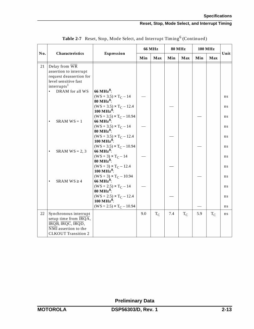
21 Delay from WR assertion to interrupt request deassertion for level sensitive fast interrupts1
• DRAM for all WS
• SRAM WS = 1
• SRAM WS = 2, 3
• SRAM WS ≥ 4
66 MHz8: (WS + 3.5) × TC – 14 80 MHz8: (WS + 3.5) × TC – 12.4100 MHz8: (WS + 3.5) × TC – 10.9466 MHz8: (WS + 3.5) × TC – 14 80 MHz8: (WS + 3.5) × TC – 12.4 100 MHz8: (WS + 3.5) × TC – 10.9466 MHz8: (WS + 3) × TC – 14 80 MHz8: (WS + 3) × TC – 12.4 100 MHz8: (WS + 3) × TC – 10.9466 MHz8: (WS + 2.5) × TC – 14 80 MHz8: (WS + 2.5) × TC – 12.4 100 MHz8: (WS + 2.5) × TC – 10.94
—
—
—
—
—
—
—
—
—
—
—
—
ns
ns
ns
ns
ns
ns
ns
ns
ns
ns
ns
ns
22 Synchronous interrupt setup time from IRQA, IRQB, IRQC, IRQD, NMI assertion to the CLKOUT Transition 2
9.0 TC 7.4 TC 5.9 TC ns
Table 2-7 Reset, Stop, Mode Select, and Interrupt Timing6 (Continued)
No. Characteristics Expression 66 MHz 80 MHz 100 MHz
UnitMin Max Min Max Min Max

Preliminary Data
2-14 DSP56303/D, Rev. 1 MOTOROLA
Specifications
Reset, Stop, Mode Select, and Interrupt Timing
23 Synchronous interrupt delay time from the CLKOUT Transition 2 to the first external address output valid caused by the first instruction fetch after coming out of Wait Processing state• Minimum• Maximum 9.25 × TC + 1.0
24.75 × TC + 5.0141.0
——
380.0116.6
——
314.493.5—
—252.5
nsns
24 Duration for IRQA assertion to recover from Stop state
9.0 — 7.4 — 5.9 — ns
25 Delay from IRQA assertion to fetch of first instruction (when exiting Stop)2, 3
• PLL is not active during Stop (PCTL Bit 17 = 0) and Stop delay is enabled (OMR Bit 6 = 0)
• PLL is not active during Stop (PCTL Bit 17 = 0) and Stop delay is not enabled (OMR Bit 6 = 1)
• PLL is active during Stop (PCTL Bit 17 = 1) (Implies No Stop Delay)
PLC × ETC × PDF + (128 K − PLC/2) × TC
PLC × ETC × PDF + (23.75 ± 0.5) × TC
(8.25 ± 0.5) × TC
2.0
352.3 ns
117.4
64.1
62.1 ms
132.6
1.6
290.6 ns
96.9
17.0
15.4 ms
109.4
1.3
232.5 ns
77.5
13.6
12.3 ms
87.5
ms
ns
Table 2-7 Reset, Stop, Mode Select, and Interrupt Timing6 (Continued)
No. Characteristics Expression 66 MHz 80 MHz 100 MHz
UnitMin Max Min Max Min Max

Specifications
Reset, Stop, Mode Select, and Interrupt Timing
Preliminary Data
MOTOROLA DSP56303/D, Rev. 1 2-15
26 Duration of level sensitive IRQA assertion to ensure interrupt service (when exiting Stop)2, 3
• PLL is not active during Stop (PCTL Bit 17 = 0) and Stop delay is enabled (OMR Bit 6 = 0)
• PLL is not active during Stop (PCTL Bit 17 = 0) and Stop delay is not enabled (OMR Bit 6 = 1)
• PLL is active during Stop (PCTL Bit 17 = 1) (implies no Stop delay)
PLC × ETC × PDF + (128K − PLC/2) × TC
PLC × ETC × PDF + (20.5 ± 0.5) × TC
5.5 × TC
64.1
62.1
83.4
—
—
—
17.0
15.4
68.8
—
—
—
13.6
12.3
55.0
—
—
—
ms
ms
ns
27 Interrupt Requests Rate• HI08, ESSI, SCI,
Timer• DMA• IRQ, NMI (edge
trigger)• IRQ, NMI (level
trigger)
12TC
8TC8TC
12TC
—
——
—
181.8
121.2121.2
181.8
—
——
—
150.0
100.0100.0
150.0
—
——
—
120.0
80.080.0
120.0
ns
nsns
ns
28 DMA Requests Rate• Data read from
HI08, ESSI, SCI• Data write to HI08,
ESSI, SCI• Timer• IRQ, NMI (edge
trigger)
6TC
7TC
2TC3TC
—
—
——
90.9
106.1
30.345.5
—
—
——
75.0
87.5
25.037.5
—
—
——
60.0
70.0
20.030.0
ns
ns
nsns
Table 2-7 Reset, Stop, Mode Select, and Interrupt Timing6 (Continued)
No. Characteristics Expression 66 MHz 80 MHz 100 MHz
UnitMin Max Min Max Min Max

Preliminary Data
2-16 DSP56303/D, Rev. 1 MOTOROLA
Specifications
Reset, Stop, Mode Select, and Interrupt Timing
29 Delay from IRQA, IRQB, IRQC, IRQD, NMI assertion to external memory (DMA source) access address out valid
4.25 × TC + 2.0 66.0 — 55.1 — 44.0 — ns
Notes: 1. When using fast interrupts and IRQA, IRQB, IRQC, and IRQD are defined as level-sensitive, timings 19 through 21 apply to prevent multiple interrupt service. To avoid these timing restrictions, the deasserted Edge-triggered mode is recommended when using fast interrupts. Long interrupts are recommended when using Level-sensitive mode.
2. This timing depends on several settings:
For PLL disable, using internal oscillator (PLL Control Register (PCTL) Bit 16 = 0) and oscillator disabled during Stop (PCTL Bit 17 = 0), a stabilization delay is required to assure the oscillator is stable before executing programs. In that case, resetting the Stop delay (OMR Bit 6 = 0) will provide the proper delay. While it is possible to set OMR Bit 6 = 1, it is not recommended and these specifications do not guarantee timings for that case.
For PLL disable, using internal oscillator (PCTL Bit 16 = 0) and oscillator enabled during Stop (PCTL Bit 17=1), no stabilization delay is required and recovery time will be minimal (OMR Bit 6 setting is ignored).
For PLL disable, using external clock (PCTL Bit 16 = 1), no stabilization delay is required and recovery time will be defined by the PCTL Bit 17 and OMR Bit 6 settings.
For PLL enable, if PCTL Bit 17 is 0, the PLL is shutdown during Stop. Recovering from Stop requires the PLL to get locked. The PLL lock procedure duration, PLL Lock Cycles (PLC), may be in the range of 0 to 1000 cycles. This procedure occurs in parallel with the stop delay counter, and stop recovery will end when the last of these two events occurs. The stop delay counter completes count or PLL lock procedure completion.
PLC value for PLL disable is 0.
The maximum value for ETC is 4096 (maximum MF) divided by the desired internal frequency (i.e., for 66 MHz it is 4096/66 MHz = 62 µs). During the stabilization period, TC, TH, and TL will not be constant, and their width may vary, so timing may vary as well.
3. Periodically sampled and not 100% tested
Table 2-7 Reset, Stop, Mode Select, and Interrupt Timing6 (Continued)
No. Characteristics Expression 66 MHz 80 MHz 100 MHz
UnitMin Max Min Max Min Max

Specifications
Reset, Stop, Mode Select, and Interrupt Timing
Preliminary Data
MOTOROLA DSP56303/D, Rev. 1 2-17
4. For an external clock generator, RESET duration is measured during the time in which RESET is asserted, VCC is valid, and the EXTAL input is active and valid.
For internal oscillator, RESET duration is measured during the time in which RESET is asserted and VCC is valid. The specified timing reflects the crystal oscillator stabilization time after power-up. This number is affected both by the specifications of the crystal and other components connected to the oscillator and reflects worst case conditions.
When the VCC is valid, but the other “required RESET duration” conditions (as specified above) have not been yet met, the device circuitry will be in an uninitialized state that can result in significant power consumption and heat-up. Designs should minimize this state to the shortest possible duration.
5. If PLL does not lose lock6. VCC = 3.3 V ± 0.3 V; TJ = –40°C to +100°C, CL = 50 pF + 2 TTL Loads7. WS = number of wait states (measured in clock cycles, number of TC)8. Use expression to compute maximum value.
Figure 2-3 Reset Timing
Figure 2-4 Synchronous Reset Timing
Table 2-7 Reset, Stop, Mode Select, and Interrupt Timing6 (Continued)
No. Characteristics Expression 66 MHz 80 MHz 100 MHz
UnitMin Max Min Max Min Max
VIH
RESET
Reset Value
First Fetch
All Pins
A0–A17
8
9 10
AA0460
CLKOUT
RESET
A0–A17
11
12
AA0461

Preliminary Data
2-18 DSP56303/D, Rev. 1 MOTOROLA
Specifications
Reset, Stop, Mode Select, and Interrupt Timing
Figure 2-5 External Fast Interrupt Timing
Figure 2-6 External Interrupt Timing (Negative Edge-Triggered)
A0–A17
RD
a) First Interrupt Instruction Execution
GeneralPurpose
I/O
IRQA,IRQB,IRQC,IRQD,
NMIb) General Purpose I/O
IRQA, IRQB,IRQC, IRQD,
NMI
WR
20
21
1917
18
AA0462
First Interrupt InstructionExecution/Fetch
IRQA, IRQB,IRQC, IRQD,
NMI
IRQA, IRQB,IRQC, IRQD,
NMI
15
16AA0463

Specifications
Reset, Stop, Mode Select, and Interrupt Timing
Preliminary Data
MOTOROLA DSP56303/D, Rev. 1 2-19
Figure 2-7 Synchronous Interrupt from Wait State Timing
Figure 2-8 Operating Mode Select Timing
Figure 2-9 Recovery from Stop State Using IRQA
CLKOUT
IRQA, IRQB,IRQC, IRQD,
NMI
A0–A17
22
23
AA0464
RESET
MODA, MODB,MODC, MODD,
PINIT
VIH
IRQA, IRQB, IRQC, IRQD, NMI
VIH
VIL
VIH
VIL
13
14
AA0465
First Instruction Fetch
IRQA
A0–A17
24
25
AA0466
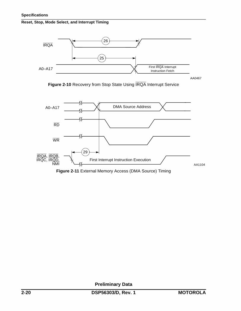
Preliminary Data
2-20 DSP56303/D, Rev. 1 MOTOROLA
Specifications
Reset, Stop, Mode Select, and Interrupt Timing
Figure 2-10 Recovery from Stop State Using IRQA Interrupt Service
Figure 2-11 External Memory Access (DMA Source) Timing
IRQA
A0–A17 First IRQA InterruptInstruction Fetch
26
25
AA0467
29
DMA Source Address
First Interrupt Instruction Execution
A0–A17
RD
WR
IRQA, IRQB,IRQC, IRQD,
NMI AA1104

Specifications
External Memory Expansion Port (Port A)
Preliminary Data
MOTOROLA DSP56303/D, Rev. 1 2-21
EXTERNAL MEMORY EXPANSION PORT (PORT A)
SRAM Timing
Table 2-8 SRAM Read and Write Accesses
No. Characteristics Symbol Expression166 MHz 80 MHz 100 MHz
Unit Min Max Min Max Min Max
100 Address valid and AA assertion pulse width
tRC, tWC (WS + 1) × TC − 4.0 [1 ≤ WS ≤ 3](WS + 2) × TC − 4.0 [4 ≤ WS ≤ 7](WS + 3) × TC − 4.0 [WS ≥ 8]
26.3
86.9
162.7
—
—
—
21.0
71.0
133.5
—
—
—
16.0
56.0
106.0
—
—
—
ns
ns
ns
101 Address and AA valid to WR assertion
tAS 66 MHz: 0.25 × TC − 3.7 [WS = 1]80 MHz: 0.25 × TC − 3.0[WS = 1]100 MHz: 0.25 × TC − 2.4[WS = 1]All frequencies:0.75 × TC − 4.0 [2 ≤ WS ≤ 3]1.25 × TC − 4.0 [WS ≥ 4]
0.1
—
—
7.4
14.9
—
—
—
—
—
—
0.1
—
5.4
11.6
—
—
—
—
—
—
—
0.1
3.5
8.5
—
—
—
—
—
ns
ns
ns
ns
ns
102 WR assertion pulse width
tWP 1.5 × TC − 4.5 [WS = 1]WS × TC − 4.0 [2 ≤ WS ≤ 3](WS − 0.5) × TC − 4.0 [WS ≥ 4]
18.2
26.3
49.0
—
—
—
14.3
21.0
39.8
—
—
—
10.5
16.0
31.0
—
—
—
ns
ns
ns

Preliminary Data
2-22 DSP56303/D, Rev. 1 MOTOROLA
Specifications
External Memory Expansion Port (Port A)
103 WR deassertion to address not valid
tWR 66 MHz: 0.25 × TC − 3.8 [1 ≤ WS ≤ 3]80 MHz: 0.25 × TC − 3.0 [1 ≤ WS ≤ 3]100 MHz: 0.25 × TC − 2.4 [1 ≤ WS ≤ 3]All frequencies:1.25 × TC − 4.0 [4 ≤ WS ≤ 7]2.25 × TC − 4.0 [WS ≥ 8]
0.1
—
—
14.9
30.1
—
—
—
—
—
—
0.1
—
11.6
24.1
—
—
—
—
—
—
—
0.1
8.5
18.5
—
—
—
—
—
ns
ns
ns
ns
ns
104 Address and AA valid to input data valid
tAA, tAC 66 MHz: (WS + 0.75) × TC − 11.0 [WS ≥ 1]80 MHz: (WS + 0.75) × TC − 9.5 [WS ≥ 1]100 MHz: (WS + 0.75) × TC − 8.0 [WS ≥ 1]
—
—
—
15.5
—
—
—
—
—
—
12.4
—
—
—
—
—
—
9.5
ns
ns
ns
105 RD assertion to input data valid
tOE 66 MHz: (WS + 0.25) × TC − 11.0 [WS ≥ 1]80 MHz: (WS + 0.25) × TC − 9.5 [WS ≥ 1]100 MHz: (WS + 0.25) × TC − 8.0 [WS ≥ 1]
—
—
—
7.9
—
—
—
—
—
—
6.1
—
—
—
—
—
—
4.5
ns
ns
ns
106 RD deassertion to data not valid (data hold time)
tOHZ 0.0 — 0.0 — 0.0 — ns
107 Address valid to WR deassertion
tAW (WS + 0.75) × TC − 4.0 [WS ≥ 1]
22.5 — 17.9 — 13.5 — ns
Table 2-8 SRAM Read and Write Accesses (Continued)
No. Characteristics Symbol Expression166 MHz 80 MHz 100 MHz
Unit Min Max Min Max Min Max

Specifications
External Memory Expansion Port (Port A)
Preliminary Data
MOTOROLA DSP56303/D, Rev. 1 2-23
108 Data valid to WR deassertion (data setup time)
tDS (tDW) 66 MHz: (WS − 0.25) × TC − 3.9 [WS ≥ 1]80 MHz: (WS − 0.25) × TC − 3.3 [WS ≥ 1]100 MHz: (WS − 0.25) × TC − 2.75 [WS ≥ 1]
7.5
—
—
—
—
—
—
6.1
—
—
—
—
—
—
4.8
—
—
—
ns
ns
ns
109 Data hold time from WR deassertion
tDH 66 MHz: 0.25 × TC − 3.7 [1 ≤ WS ≤ 3]80 MHz: 0.25 × TC − 3.0 [1 ≤ WS ≤ 3]100 MHz: 0.25 × TC − 2.4 [1 ≤ WS ≤ 3]All frequencies:1.25 × TC − 3.8[4 ≤ WS ≤ 7]2.25 × TC − 3.8 [WS ≥ 8]
0.1
—
—
15.2
30.4
—
—
—
—
—
—
0.1
—
11.8
24.3
—
—
—
—
—
—
—
0.1
8.7
18.7
—
—
—
—
—
ns
ns
ns
ns
ns
110 WR assertion to data active
0.75 × TC − 3.7 [WS = 1]0.25 × TC − 3.7 [2 ≤ WS ≤ 3]−0.25 × TC − 3.7 [WS ≥ 4]
7.7
0.1
–7.5
—
—
—
5.7
–0.6
–6.8
—
—
—
3.8
–1.2
–6.2
—
—
—
ns
ns
ns
111 WR deassertion to data high impedance
0.25 × TC + 0.2 [1 ≤ WS ≤ 3]1.25 × TC + 0.2 [4 ≤ WS ≤ 7]2.25 × TC + 0.2 [WS ≥ 8]
—
—
—
4.0
19.1
34.3
—
—
—
3.3
15.8
28.3
—
—
—
2.7
12.7
22.7
ns
ns
ns
112 Previous RD deassertion to data active (write)
1.25 × TC − 4.0 [1 ≤ WS ≤ 3]2.25 × TC − 4.0 [4 ≤ WS ≤ 7]3.25 × TC − 4.0 [WS ≥ 8]
14.9
30.1
45.2
—
—
—
11.6
24.1
36.6
—
—
—
8.5
18.5
28.5
—
—
—
ns
ns
ns
Table 2-8 SRAM Read and Write Accesses (Continued)
No. Characteristics Symbol Expression166 MHz 80 MHz 100 MHz
Unit Min Max Min Max Min Max

Preliminary Data
2-24 DSP56303/D, Rev. 1 MOTOROLA
Specifications
External Memory Expansion Port (Port A)
113 RD deassertion time
0.75 × TC − 4.0 [1 ≤ WS ≤ 3]1.75 × TC − 4.0 [4 ≤ WS ≤ 7]2.75 × TC − 4.0 [WS ≥ 8]
7.4
22.5
37.7
—
—
—
5.4
17.9
30.4
—
—
—
3.5
13.5
23.5
—
—
—
ns
ns
ns
114 WR deassertion time
0.5 × TC − 3.5 [WS = 1]TC − 3.5 [2 ≤ WS ≤ 3]2.5 × TC − 3.5 [4 ≤ WS ≤ 7]3.5 × TC − 3.5 [WS ≥ 8]
4.1
11.7
34.4
49.5
—
—
—
—
2.8
9.0
27.8
40.3
—
—
—
—
1.5
6.5
21.5
31.5
—
—
—
—
ns
ns
ns
ns
115 Address valid to RD assertion
0.5 × TC − 4 3.5 — 2.3 — 1.0 — ns
116 RD assertion pulse width
(WS + 0.25) × TC − 3.8 15.1 — 11.8 — 8.7 — ns
117 RD deassertion to address not valid
0.25 × TC − 3.0 [1 ≤ WS ≤ 3]1.25 × TC − 3.0 [4 ≤ WS ≤ 7]2.25 × TC − 3.0 [WS ≥ 8]
0.7
15.9
31.0
—
—
—
0.1
12.6
25.1
—
—
—
0.0
9.5
19.5
—
—
—
ns
ns
ns
Notes: 1. WS is the number of wait states specified in the BCR.2. VCC = 3.3 V ± 0.3 V; TJ = –40°C to +100 °C, CL = 50 pF + 2 TTL Loads
Table 2-8 SRAM Read and Write Accesses (Continued)
No. Characteristics Symbol Expression166 MHz 80 MHz 100 MHz
Unit Min Max Min Max Min Max

Specifications
External Memory Expansion Port (Port A)
Preliminary Data
MOTOROLA DSP56303/D, Rev. 1 2-25
Figure 2-12 SRAM Read Access
Figure 2-13 SRAM Write Access
A0–A17
RD
WR
DataInD0–D23
AA0–AA3
115 105 106
113
104
116 117
100
AA0468
A0–A17
WR
RD
DataOutD0–D23
AA0–AA3
100
102101
107
114
110
112
103
111108
109
AA0469

Preliminary Data
2-26 DSP56303/D, Rev. 1 MOTOROLA
Specifications
External Memory Expansion Port (Port A)
DRAM Timing
The selection guides provided in Figure 2-14 and Figure 2-17 on page 2-37 should be used for primary selection only. Final selection should be based on the timing provided in the following tables. As an example, the selection guide suggests that 4 wait states must be used for 100 MHz operation when using Page Mode DRAM. However, by using the information in the appropriate table, a designer may choose to evaluate whether fewer wait states might be used by determining which timing prevents operation at 100 MHz, running the chip at a slightly lower frequency (e.g., 95 MHz), using faster DRAM (if it becomes available), and control factors such as capacitive and resistive load to improve overall system performance.
Figure 2-14 DRAM Page Mode Wait States Selection Guide
Chip Frequency(MHz)
DRAM Type(tRAC ns)
100
80
70
60
40 66 80 100
1 Wait States
2 Wait States
3 Wait States
4 Wait States
Note: This figure should be use for primary selection. For exact and detailed timings see the following tables.
AA0472
50120

Specifications
External Memory Expansion Port (Port A)
Preliminary Data
MOTOROLA DSP56303/D, Rev. 1 2-27
Table 2-9 DRAM Page Mode Timings, One Wait State (Low-Power Applications)1, 2, 3
No. Characteristics Symbol Expression20 MHz6 30 MHz6
UnitMin Max Min Max
131 Page mode cycle time tPC 1.25 × TC 62.5 — 41.7 — ns
132 CAS assertion to data valid (read)
tCAC TC − 7.5 — 42.5 — 25.8 ns
133 Column address valid to data valid (read)
tAA 1.5 × TC − 7.5 — 67.5 — 42.5 ns
134 CAS deassertion to data not valid (read hold time)
tOFF 0.0 — 0.0 — ns
135 Last CAS assertion to RAS deassertion
tRSH 0.75 × TC − 4.0 33.5 — 21.0 — ns
136 Previous CAS deassertion to RAS deassertion
tRHCP 2 × TC − 4.0 96.0 — 62.7 — ns
137 CAS assertion pulse width tCAS 0.75 × TC − 4.0 33.5 — 21.0 — ns
138 Last CAS deassertion to RAS deassertion4
• BRW[1:0] = 00• BRW[1:0] = 01• BRW[1:0] = 10• BRW[1:0] = 11
tCRP
1.75 × TC − 6.03.25 × TC − 6.04.25 × TC − 6.06.25 × TC – 6.0
81.5156.5206.5306.5
————
52.3102.2135.5202.1
————
nsnsnsns
139 CAS deassertion pulse width
tCP 0.5 × TC − 4.0 21.0 — 12.7 — ns
140 Column address valid to CAS assertion
tASC 0.5 × TC − 4.0 21.0 — 12.7 — ns
141 CAS assertion to column address not valid
tCAH 0.75 × TC − 4.0 33.5 — 21.0 — ns
142 Last column address valid to RAS deassertion
tRAL 2 × TC − 4.0 96.0 — 62.7 — ns
143 WR deassertion to CAS assertion
tRCS 0.75 × TC − 3.8 33.7 — 21.2 — ns
144 CAS deassertion to WR assertion
tRCH 0.25 × TC − 3.7 8.8 — 4.6 — ns
145 CAS assertion to WR deassertion
tWCH 0.5 × TC − 4.2 20.8 — 12.5 — ns
146 WR assertion pulse width tWP 1.5 × TC − 4.5 70.5 — 45.5 — ns
147 Last WR assertion to RAS deassertion
tRWL 1.75 × TC − 4.3 83.2 — 54.0 — ns

Preliminary Data
2-28 DSP56303/D, Rev. 1 MOTOROLA
Specifications
External Memory Expansion Port (Port A)
148 WR assertion to CAS deassertion
tCWL 1.75 × TC − 4.3 83.2 — 54.0 — ns
149 Data valid to CAS assertion (Write)
tDS 0.25 × TC − 4.0 8.5 — 4.3 — ns
150 CAS assertion to data not valid (write)
tDH 0.75 × TC − 4.0 33.5 — 21.0 — ns
151 WR assertion to CAS assertion
tWCS TC − 4.3 45.7 — 29.0 — ns
152 Last RD assertion to RAS deassertion
tROH 1.5 × TC − 4.0 71.0 — 46.0 — ns
153 RD assertion to data valid tGA TC − 7.5 — 42.5 — 25.8 ns
154 RD deassertion to data not valid 5
tGZ 0.0 — 0.0 — ns
155 WR assertion to data active 0.75 × TC − 0.3 37.2 — 24.7 — ns
156 WR deassertion to data high impedance
0.25 × TC — 12.5 — 8.3 ns
Notes: 1. The number of wait states for Page mode access is specified in the DCR.2. The refresh period is specified in the DCR.3. All the timings are calculated for the worst case. Some of the timings are better for specific cases (e.g.,
tPC equals 2 × TC for read-after-read or write-after-write sequences).4. BRW[1:0] (DRAM control register bits) defines the number of wait states that should be inserted in each
DRAM out-of-page access.5. RD deassertion will always occur after CAS deassertion; therefore, the restricted timing is tOFF and not
tGZ.6. Reduced DSP clock speed allows use of Page Mode DRAM with one Wait state (see Figure 2-14).
Table 2-9 DRAM Page Mode Timings, One Wait State (Low-Power Applications)1, 2, 3
No. Characteristics Symbol Expression20 MHz6 30 MHz6
UnitMin Max Min Max

Specifications
External Memory Expansion Port (Port A)
Preliminary Data
MOTOROLA DSP56303/D, Rev. 1 2-29
Table 2-10 DRAM Page Mode Timings, Two Wait States1, 2, 3, 7
No. Characteristics Symbol Expression66 MHz 80 MHz
Unit Min Max Min Max
131 Page mode cycle time tPC 2.75 × TC 41.7 — 34.4 — ns
132 CAS assertion to data valid (read)
tCAC 66 MHz: 1.5 × TC − 7.580 MHz: 1.5 × TC − 6.5
—
—
15.2
—
—
—
—
12.3
ns
ns
133 Column address valid to data valid (read)
tAA 66 MHz: 2.5 × TC − 7.580 MHz: 2.5 × TC − 6.5
—
—
30.4
—
—
—
—
24.8
ns
ns
134 CAS deassertion to data not valid (read hold time)
tOFF 0.0 — 0.0 — ns
135 Last CAS assertion to RAS deassertion
tRSH 1.75 × TC − 4.0 22.5 — 17.9 — ns
136 Previous CAS deassertion to RAS deassertion
tRHCP 3.25 × TC − 4.0 45.2 — 36.6 — ns
137 CAS assertion pulse width tCAS 1.5 × TC − 4.0 18.7 — 14.8 — ns
138 Last CAS deassertion to RAS deassertion5
• BRW[1:0] = 00• BRW[1:0] = 01• BRW[1:0] = 10• BRW[1:0] = 11
tCRP
2.0 × TC − 6.03.5 × TC − 6.04.5 × TC − 6.06.5 × TC − 6.0
24.447.262.492.8
————
19.037.850.375.3
————
nsnsnsns
139 CAS deassertion pulse width
tCP 1.25 × TC − 4.0 14.9 — 11.6 — ns
140 Column address valid to CAS assertion
tASC TC − 4.0 11.2 — 8.5 — ns
141 CAS assertion to column address not valid
tCAH 1.75 × TC − 4.0 22.5 — 17.9 — ns
142 Last column address valid to RAS deassertion
tRAL 3 × TC − 4.0 41.5 — 33.5 — ns
143 WR deassertion to CAS assertion
tRCS 1.25 × TC − 3.8 15.1 — 11.8 — ns
144 CAS deassertion to WR assertion
tRCH 0.5 × TC − 3.7 3.9 — 2.6 — ns
145 CAS assertion to WR deassertion
tWCH 1.5 × TC − 4.2 18.5 — 14.6 — ns
146 WR assertion pulse width tWP 2.5 × TC − 4.5 33.4 — 26.8 — ns

Preliminary Data
2-30 DSP56303/D, Rev. 1 MOTOROLA
Specifications
External Memory Expansion Port (Port A)
147 Last WR assertion to RAS deassertion
tRWL 2.75 × TC − 4.3 37.4 — 30.1 — ns
148 WR assertion to CAS deassertion
tCWL 2.5 × TC − 4.3 33.6 — 27.0 — ns
149 Data valid to CAS assertion (write)
tDS 66 MHz: 0.25 × TC − 3.780 MHz: 0.25 × TC − 3.0
0.1
—
—
—
—
0.1
—
—
ns
ns
150 CAS assertion to data not valid (write)
tDH 1.75 × TC − 4.0 22.5 — 17.9 — ns
151 WR assertion to CAS assertion
tWCS TC − 4.3 10.9 — 8.2 — ns
152 Last RD assertion to RAS deassertion
tROH 2.5 × TC − 4.0 33.9 — 27.3 — ns
153 RD assertion to data valid tGA 66 MHz: 1.75 × TC − 7.580 MHz: 1.75 × TC − 6.5
—
—
19.0
—
—
—
—
15.4
ns
ns
154 RD deassertion to data not valid6
tGZ 0.0 — 0.0 — ns
155 WR assertion to data active 0.75 × TC − 0.3 11.1 — 9.1 — ns
156 WR deassertion to data high impedance
0.25 × TC — 3.8 — 3.1 ns
Notes: 1. The number of wait states for Page mode access is specified in the DCR.2. The refresh period is specified in the DCR.3. The asynchronous delays specified in the expressions are valid for DSP56303.4. All the timings are calculated for the worst case. Some of the timings are better for specific cases (e.g.,
tPC equals 3 × TC for read-after-read or write-after-write sequences).5. BRW[1:0] (DRAM Control Register bits) defines the number of wait states that should be inserted in
each DRAM out-of-page access.6. RD deassertion will always occur after CAS deassertion; therefore, the restricted timing is tOFF and not
tGZ.7. There are not any fast enough DRAMs to fit to two wait states Page mode @ 100MHz (see
Figure 2-14)
Table 2-10 DRAM Page Mode Timings, Two Wait States1, 2, 3, 7 (Continued)
No. Characteristics Symbol Expression66 MHz 80 MHz
Unit Min Max Min Max

Specifications
External Memory Expansion Port (Port A)
Preliminary Data
MOTOROLA DSP56303/D, Rev. 1 2-31
Table 2-11 DRAM Page Mode Timings, Three Wait States1, 2, 3
No. Characteristics Symbol Expression66 MHz 80 MHz 100 MHz
Unit Min Max Min Max Min Max
131 Page mode cycle time tPC 3.5 × TC 53.0 — 43.8 — 35.0 — ns
132 CAS assertion to data valid (read)
tCAC 66 MHz: 2 × TC − 7.580 MHz: 2 × TC − 6.5100 MHz: 2 × TC − 5.7
—
—
—
22.8
—
—
—
—
—
—
18.5
—
—
—
—
—
—
14.3
ns
ns
ns
133 Column address valid to data valid (read)
tAA 66 MHz: 3 × TC − 7.580 MHz: 3 × TC − 6.5100 MHz: 3 × TC − 5.7
—
—
—
37.9
—
—
—
—
—
—
31.0
—
—
—
—
—
—
24.3
ns
ns
ns
134 CAS deassertion to data not valid (read hold time)
tOFF 0.0 — 0.0 — 0.0 — ns
135 Last CAS assertion to RAS deassertion
tRSH 2.5 × TC − 4.0 33.9 — 27.3 — 21.0 — ns
136 Previous CAS deassertion to RAS deassertion
tRHCP 4.5 × TC − 4.0 64.2 — 52.3 — 41.0 — ns
137 CAS assertion pulse width tCAS 2 × TC − 4.0 26.3 — 21.0 — 16.0 — ns
138 Last CAS deassertion to RAS deassertion5
• BRW[1:0] = 00• BRW[1:0] = 01• BRW[1:0] = 10• BRW[1:0] = 11
tCRP
2.25 × TC − 6.03.75 × TC − 6.04.75 × TC − 6.06.75 × TC − 6.0
28.251.066.296.6
————
22.240.953.478.4
————
16.531.541.561.5
————
nsnsnsns
139 CAS deassertion pulse width tCP 1.5 × TC − 4.0 18.7 — 14.8 — 11.0 — ns
140 Column address valid to CAS assertion
tASC TC − 4.0 11.2 — 8.5 — 6.0 — ns
141 CAS assertion to column address not valid
tCAH 2.5 × TC − 4.0 33.9 — 27.3 — 21.0 — ns
142 Last column address valid to RAS deassertion
tRAL 4 × TC − 4.0 56.6 — 46.0 — 36.0 — ns
143 WR deassertion to CAS assertion
tRCS 1.25 × TC − 3.8 15.1 — 11.8 — 8.7 — ns
144 CAS deassertion to WR assertion
tRCH 0.75 × TC − 3.7 7.7 — 5.7 — 3.8 — ns

Preliminary Data
2-32 DSP56303/D, Rev. 1 MOTOROLA
Specifications
External Memory Expansion Port (Port A)
145 CAS assertion to WR deassertion
tWCH 2.25 × TC − 4.2 29.9 — 23.9 — 18.3 — ns
146 WR assertion pulse width tWP 3.5 × TC − 4.5 48.5 — 39.3 — 30.5 — ns
147 Last WR assertion to RAS deassertion
tRWL 3.75 × TC − 4.3 52.5 — 42.6 — 33.2 — ns
148 WR assertion to CAS deassertion
tCWL 3.25 × TC − 4.3 44.9 — 36.3 — 28.2 — ns
149 Data valid to CAS assertion (write)
tDS 0.5 × TC − 4.0 3.6 — 2.3 — 1.0 — ns
150 CAS assertion to data not valid (write)
tDH 2.5 × TC − 4.0 33.9 — 27.3 — 21.0 — ns
151 WR assertion to CAS assertion tWCS 1.25 × TC − 4.3 14.6 — 11.3 — 8.2 — ns
152 Last RD assertion to RAS deassertion
tROH 3.5 × TC − 4.0 49.0 — 39.8 — 31.0 — ns
153 RD assertion to data valid tGA 66 MHz: 2.5 × TC − 7.580 MHz: 2.5 × TC − 6.5100 MHz: 2.5 × TC − 5.7
—
—
—
30.4
—
—
—
—
—
—
24.8
—
—
—
—
—
—
19.3
ns
ns
ns
154 RD deassertion to data not valid6
tGZ 0.0 — 0.0 — 0.0 — ns
155 WR assertion to data active 0.75 × TC − 0.3 11.1 — 9.1 — 7.2 — ns
156 WR deassertion to data high impedance
0.25 × TC — 3.8 — 3.1 — 2.5 ns
Notes: 1. The number of wait states for Page mode access is specified in the DCR.2. The refresh period is specified in the DCR.3. The asynchronous delays specified in the expressions are valid for DSP56303.4. All the timings are calculated for the worst case. Some of the timings are better for specific cases (e.g.,
tPC equals 4 × TC for read-after-read or write-after-write sequences).5. BRW[1:0] (DRAM control register bits) defines the number of wait states that should be inserted in each
DRAM out-of page-access.6. RD deassertion will always occur after CAS deassertion; therefore, the restricted timing is tOFF and not
tGZ.
Table 2-11 DRAM Page Mode Timings, Three Wait States1, 2, 3 (Continued)
No. Characteristics Symbol Expression66 MHz 80 MHz 100 MHz
Unit Min Max Min Max Min Max

Specifications
External Memory Expansion Port (Port A)
Preliminary Data
MOTOROLA DSP56303/D, Rev. 1 2-33
Table 2-12 DRAM Page Mode Timings, Four Wait States1, 2, 3
No. Characteristics Symbol Expression66 MHz 80 MHz 100 MHz
Unit Min Max Min Max Min Max
131 Page mode cycle time tPC 4.5 × TC 68.2 — 56.3 — 45.0 — ns
132 CAS assertion to data valid (read)
tCAC 66 MHz: 2.75 × TC − 7.580 MHz:2.75 × TC − 6.5100 MHz:2.75 × TC − 5.7
—
—
—
34.2
—
—
—
—
—
—
27.9
—
—
—
—
—
—
21.8
ns
ns
ns
133 Column address valid to data valid (read)
tAA 66 MHz: 3.75 × TC − 7.580 MHz:3.75 × TC − 6.5100 MHz:3.75 × TC − 5.7
—
—
—
49.3
—
—
—
—
—
—
40.4
—
—
—
—
—
—
31.8
ns
ns
ns
134 CAS deassertion to data not valid (read hold time)
tOFF 0.0 — 0.0 — 0.0 — ns
135 Last CAS assertion to RAS deassertion
tRSH 3.5 × TC − 4.0 49.0 — 39.8 — 31.0 — ns
136 Previous CAS deassertion to RAS deassertion
tRHCP 6 × TC − 4.0 86.9 — 71.0 — 56.0 — ns
137 CAS assertion pulse width tCAS 2.5 × TC − 4.0 33.9 — 27.3 — 21.0 — ns
138 Last CAS deassertion to RAS deassertion5
• BRW[1:0] = 00• BRW[1:0] = 01• BRW[1:0] = 10• BRW[1:0] = 11
tCRP
2.75 × TC − 6.04.25 × TC − 6.05.25 × TC − 6.06.25 × TC − 6.0
35.858.673.889.0
————
28.447.259.772.2
————
21.536.546.556.5
————
nsnsnsns
139 CAS deassertion pulse width
tCP 2 × TC − 4.0 26.3 — 21.0 — 16.0 — ns
140 Column address valid to CAS assertion
tASC TC − 4.0 11.2 — 8.5 — 6.0 — ns
141 CAS assertion to column address not valid
tCAH 3.5 × TC − 4.0 49.0 — 39.8 — 31.0 — ns
142 Last column address valid to RAS deassertion
tRAL 5 × TC − 4.0 71.8 — 58.5 — 46.0 — ns
143 WR deassertion to CAS assertion
tRCS 1.25 × TC − 3.8 15.1 — 11.8 — 8.7 — ns
144 CAS deassertion to WR assertion
tRCH 1.25 × TC − 3.7 15.2 — 11.9 — 8.8 — ns
Preliminary Data
2-34 DSP56303/D, Rev. 1 MOTOROLA
Specifications
External Memory Expansion Port (Port A)
145 CAS assertion to WR deassertion
tWCH 3.25 × TC − 4.2 45.0 — 36.4 — 28.3 — ns
146 WR assertion pulse width tWP 4.5 × TC − 4.5 63.7 — 51.8 — 40.5 — ns
147 Last WR assertion to RAS deassertion
tRWL 4.75 × TC − 4.3 67.7 — 55.1 — 43.2 — ns
148 WR assertion to CAS deassertion
tCWL 3.75 × TC − 4.3 52.5 — 42.6 — 33.2 — ns
149 Data valid to CAS assertion (write)
tDS 0.5 × TC − 4.0 3.6 — 2.3 — 1.0 — ns
150 CAS assertion to data not valid (write)
tDH 3.5 × TC − 4.0 49.0 — 39.8 — 31.0 — ns
151 WR assertion to CAS assertion
tWCS 1.25 × TC − 4.3 14.6 — 11.3 — 8.2 — ns
152 Last RD assertion to RAS deassertion
tROH 4.5 × TC − 4.0 64.2 — 52.3 — 41.0 — ns
153 RD assertion to data valid tGA 66 MHz: 3.25 × TC − 7.580 MHz:3.25 × TC − 6.5100 MHz:3.25 × TC − 5.7
—
—
—
41.7
—
—
—
—
—
—
34.1
—
—
—
—
—
—
26.8
ns
ns
ns
154 RD deassertion to data not valid6
tGZ 0.0 — 0.0 — 0.0 — ns
155 WR assertion to data active 0.75 × TC − 0.3 11.1 — 9.1 — 7.2 — ns
156 WR deassertion to data high impedance
0.25 × TC — 3.8 — 3.1 — 2.5 ns
Notes: 1. The number of wait states for Page mode access is specified in the DCR.2. The refresh period is specified in the DCR.3. The asynchronous delays specified in the expressions are valid for DSP56303.4. All the timings are calculated for the worst case. Some of the timings are better for specific cases (e.g.,
tPC equals 3 × TC for read-after-read or write-after-write sequences).5. BRW[1:0] (DRAM control register bits) defines the number of wait states that should be inserted in each
DRAM out-of-page access.6. RD deassertion will always occur after CAS deassertion; therefore, the restricted timing is tOFF and not
tGZ.
Table 2-12 DRAM Page Mode Timings, Four Wait States1, 2, 3 (Continued)
No. Characteristics Symbol Expression66 MHz 80 MHz 100 MHz
Unit Min Max Min Max Min Max

Specifications
External Memory Expansion Port (Port A)
Preliminary Data
MOTOROLA DSP56303/D, Rev. 1 2-35
Figure 2-15 DRAM Page Mode Write Accesses
RAS
CAS
A0–A17
WR
RD
D0–D23
ColumnRow
Data Out Data Out Data Out
Last ColumnColumnAdd Address Address Address
136
135131
139
141
137140
142
147
144151
148146
155 156
150
138
145143
149
AA0473

Preliminary Data
2-36 DSP56303/D, Rev. 1 MOTOROLA
Specifications
External Memory Expansion Port (Port A)
Figure 2-16 DRAM Page Mode Read Accesses
RAS
CAS
A0–A17
WR
RD
D0–D23
Column Last ColumnColumnRow
Data In Data InData In
Add Address Address Address
136
135131
137
140141 142
143
152133
153
132
138139
134
154
AA0474

Specifications
External Memory Expansion Port (Port A)
Preliminary Data
MOTOROLA DSP56303/D, Rev. 1 2-37
Figure 2-17 DRAM Out-of-Page Wait States Selection Guide
Table 2-13 DRAM Out-of-Page and Refresh Timings, Four Wait States1, 2
No. Characteristics3 Symbol Expression20 MHz4 30 MHz4
UnitMin Max Min Max
157 Random read or write cycle time
tRC 5 × TC 250.0 — 166.7 — ns
158 RAS assertion to data valid (read)
tRAC 2.75 × TC − 7.5 — 130.0 — 84.2 ns
159 CAS assertion to data valid (read)
tCAC 1.25 × TC − 7.5 — 55.0 — 34.2 ns
160 Column address valid to data valid (read)
tAA 1.5 × TC − 7.5 — 67.5 — 42.5 ns
161 CAS deassertion to data not valid (read hold time)
tOFF 0.0 — 0.0 — ns
Chip Frequency(MHz)
DRAM Type(tRAC ns)
100
80
70
5066 80 100
4 Wait States
8 Wait States
11 Wait States
15 Wait States
Note: This figure should be use for primary selection. For exact and detailed timings see the following tables.
60
40 120
AA0475

Preliminary Data
2-38 DSP56303/D, Rev. 1 MOTOROLA
Specifications
External Memory Expansion Port (Port A)
162 RAS deassertion to RAS assertion
tRP 1.75 × TC − 4.0 83.5 — 54.3 — ns
163 RAS assertion pulse width
tRAS 3.25 × TC − 4.0 158.5 — 104.3 — ns
164 CAS assertion to RAS deassertion
tRSH 1.75 × TC − 4.0 83.5 — 54.3 — ns
165 RAS assertion to CAS deassertion
tCSH 2.75 × TC − 4.0 133.5 — 87.7 — ns
166 CAS assertion pulse width
tCAS 1.25 × TC − 4.0 58.5 — 37.7 — ns
167 RAS assertion to CAS assertion
tRCD 1.5 × TC ± 2 73.0 77.0 48.0 52.0 ns
168 RAS assertion to column address valid
tRAD 1.25 × TC ± 2 60.5 64.5 39.7 43.7 ns
169 CAS deassertion to RAS assertion
tCRP 2.25 × TC − 4.0 108.5 — 71.0 — ns
170 CAS deassertion pulse width
tCP 1.75 × TC − 4.0 83.5 — 54.3 — ns
171 Row address valid to RAS assertion
tASR 1.75 × TC − 4.0 83.5 — 54.3 — ns
172 RAS assertion to row address not valid
tRAH 1.25 × TC − 4.0 58.5 — 37.7 — ns
173 Column address valid to CAS assertion
tASC 0.25 × TC − 4.0 8.5 — 4.3 — ns
174 CAS assertion to column address not valid
tCAH 1.75 × TC − 4.0 83.5 — 54.3 — ns
175 RAS assertion to column address not valid
tAR 3.25 × TC − 4.0 158.5 — 104.3 — ns
176 Column address valid to RAS deassertion
tRAL 2 × TC − 4.0 96.0 — 62.7 — ns
177 WR deassertion to CAS assertion
tRCS 1.5 × TC − 3.8 71.2 — 46.2 — ns
178 CAS deassertion to WR assertion
tRCH 0.75 × TC − 3.7 33.8 — 21.3 — ns
179 RAS deassertion to WR assertion
tRRH 0.25 × TC − 3.7 8.8 — 4.6 — ns
Table 2-13 DRAM Out-of-Page and Refresh Timings, Four Wait States1, 2 (Continued)
No. Characteristics3 Symbol Expression20 MHz4 30 MHz4
UnitMin Max Min Max

Specifications
External Memory Expansion Port (Port A)
Preliminary Data
MOTOROLA DSP56303/D, Rev. 1 2-39
180 CAS assertion to WR deassertion
tWCH 1.5 × TC − 4.2 70.8 — 45.8 — ns
181 RAS assertion to WR deassertion
tWCR 3 × TC − 4.2 145.8 — 95.8 — ns
182 WR assertion pulse width
tWP 4.5 × TC − 4.5 220.5 — 145.5 — ns
183 WR assertion to RAS deassertion
tRWL 4.75 × TC − 4.3 233.2 — 154.0 — ns
184 WR assertion to CAS deassertion
tCWL 4.25 × TC − 4.3 208.2 — 137.4 — ns
185 Data valid to CAS assertion (write)
tDS 2.25 × TC − 4.0 108.5 — 71.0 — ns
186 CAS assertion to data not valid (write)
tDH 1.75 × TC − 4.0 83.5 — 54.3 — ns
187 RAS assertion to data not valid (write)
tDHR 3.25 × TC − 4.0 158.5 — 104.3 — ns
188 WR assertion to CAS assertion
tWCS 3 × TC − 4.3 145.7 — 95.7 — ns
189 CAS assertion to RAS assertion (refresh)
tCSR 0.5 × TC − 4.0 21.0 — 12.7 — ns
190 RAS deassertion to CAS assertion (refresh)
tRPC 1.25 × TC − 4.0 58.5 — 37.7 — ns
191 RD assertion to RAS deassertion
tROH 4.5 × TC − 4.0 221.0 — 146.0 — ns
192 RD assertion to data valid
tGA 4 × TC − 7.5 — 192.5 — 125.8 ns
193 RD deassertion to data not valid3
tGZ 0.0 — 0.0 — ns
194 WR assertion to data active
0.75 × TC − 0.3 37.2 — 24.7 — ns
195 WR deassertion to data high impedance
0.25 × TC — 12.5 — 8.3 ns
Notes: 1. The number of wait states for out of page access is specified in the DCR.2. The refresh period is specified in the DCR.3. RD deassertion will always occur after CAS deassertion; therefore, the restricted timing is tOFF and not
tGZ. 4. Reduced DSP clock speed allows use of DRAM out-of-page access with four Wait states (see
Figure 2-17).
Table 2-13 DRAM Out-of-Page and Refresh Timings, Four Wait States1, 2 (Continued)
No. Characteristics3 Symbol Expression20 MHz4 30 MHz4
UnitMin Max Min Max

Preliminary Data
2-40 DSP56303/D, Rev. 1 MOTOROLA
Specifications
External Memory Expansion Port (Port A)
Table 2-14 DRAM Out-of-Page and Refresh Timings, Eight Wait States1, 2
No. Characteristics4 Symbol Expression366 MHz 80 MHz 100 MHz
Unit Min Max Min Max Min Max
157 Random read or write cycle time
tRC 9 × TC 136.4 — 112.5 — 90.0 — ns
158 RAS assertion to data valid (read)
tRAC 66 MHz: 4.75 × TC − 7.580 MHz: 4.75 × TC − 6.5100 MHz: 4.75 × TC − 5.7
—
—
—
64.5
—
—
—
—
—
—
52.9
—
—
—
—
—
—
41.8
ns
ns
ns
159 CAS assertion to data valid (read)
tCAC 66 MHz: 2.25 × TC − 7.580 MHz: 2.25 × TC − 6.5100 MHz: 2.25 × TC − 5.7
—
—
—
26.6
—
—
—
—
—
—
21.6
—
—
—
—
—
—
16.8
ns
ns
ns
160 Column address valid to data valid (read)
tAA 66 MHz: 3 × TC − 7.580 MHz: 3 × TC − 6.5100 MHz: 3 × TC − 5.7
—
—
—
40.0
—
—
—
—
—
—
31.0
—
—
—
—
—
—
24.3
ns
ns
ns
161 CAS deassertion to data not valid (read hold time)
tOFF 0.0 — 0.0 — 0.0 — ns
162 RAS deassertion to RAS assertion
tRP 3.25 × TC − 4.0 45.2 — 36.6 — 28.5 — ns
163 RAS assertion pulse width tRAS 5.75 × TC − 4.0 83.1 — 67.9 — 53.5 — ns
164 CAS assertion to RAS deassertion
tRSH 3.25 × TC − 4.0 45.2 — 36.6 — 28.5 — ns
165 RAS assertion to CAS deassertion
tCSH 4.75 × TC − 4.0 68.0 — 55.4 — 43.5 — ns
166 CAS assertion pulse width tCAS 2.25 × TC − 4.0 30.1 — 24.1 — 18.5 — ns
167 RAS assertion to CAS assertion
tRCD 2.5 × TC ± 2 35.9 39.9 29.3 33.3 23.0 27.0 ns
168 RAS assertion to column address valid
tRAD 1.75 × TC ± 2 24.5 28.5 19.9 23.9 15.5 19.5 ns
169 CAS deassertion to RAS assertion
tCRP 4.25 × TC − 4.0 59.8 — 49.1 — 38.5 — ns
170 CAS deassertion pulse width
tCP 2.75 × TC − 4.0 37.7 — 30.4 — 23.5 — ns

Specifications
External Memory Expansion Port (Port A)
Preliminary Data
MOTOROLA DSP56303/D, Rev. 1 2-41
171 Row address valid to RAS assertion
tASR 3.25 × TC − 4.0 45.2 — 36.6 — 28.5 — ns
172 RAS assertion to row address not valid
tRAH 1.75 × TC − 4.0 22.5 — 17.9 — 13.5 — ns
173 Column address valid to CAS assertion
tASC 0.75 × TC − 4.0 7.4 — 5.4 — 3.5 — ns
174 CAS assertion to column address not valid
tCAH 3.25 × TC − 4.0 45.2 — 36.6 — 28.5 — ns
175 RAS assertion to column address not valid
tAR 5.75 × TC − 4.0 83.1 — 67.9 — 53.5 — ns
176 Column address valid to RAS deassertion
tRAL 4 × TC − 4.0 56.6 — 46.0 — 36.0 — ns
177 WR deassertion to CAS assertion
tRCS 2 × TC − 3.8 26.5 — 21.2 — 16.2 — ns
178 CAS deassertion to WR5 assertion
tRCH 1.25 × TC − 3.7 15.2 — 11.9 — 8.8 — ns
179 RAS deassertion to WR5 assertion
tRRH 66 MHz: 0.25 × TC − 3.780 MHz:0.25 × TC − 3.0100 MHz:0.25 × TC − 2.4
0.1
—
—
—
—
—
—
0.1
—
—
—
—
—
—
0.1
—
—
—
ns
ns
ns
180 CAS assertion to WR deassertion
tWCH 3 × TC − 4.2 41.3 — 33.3 — 25.8 — ns
181 RAS assertion to WR deassertion
tWCR 5.5 × TC − 4.2 79.1 — 64.6 — 50.8 — ns
182 WR assertion pulse width tWP 8.5 × TC − 4.5 124.3 — 101.8 — 80.5 — ns
183 WR assertion to RAS deassertion
tRWL 8.75 × TC − 4.3 128.3 — 105.1 — 83.2 — ns
184 WR assertion to CAS deassertion
tCWL 7.75 × TC − 4.3 113.1 — 92.6 — 73.2 — ns
185 Data valid to CAS assertion (write)
tDS 4.75 × TC − 4.0 68.0 — 55.4 — 43.5 — ns
186 CAS assertion to data not valid (write)
tDH 3.25 × TC − 4.0 45.2 — 36.6 — 28.5 — ns
187 RAS assertion to data not valid (write)
tDHR 5.75 × TC − 4.0 83.1 — 67.9 — 53.5 — ns
Table 2-14 DRAM Out-of-Page and Refresh Timings, Eight Wait States1, 2 (Continued)
No. Characteristics4 Symbol Expression366 MHz 80 MHz 100 MHz
Unit Min Max Min Max Min Max

Preliminary Data
2-42 DSP56303/D, Rev. 1 MOTOROLA
Specifications
External Memory Expansion Port (Port A)
188 WR assertion to CAS assertion
tWCS 5.5 × TC − 4.3 79.0 — 64.5 — 50.7 — ns
189 CAS assertion to RAS assertion (refresh)
tCSR 1.5 × TC − 4.0 18.7 — 14.8 — 11.0 — ns
190 RAS deassertion to CAS assertion (refresh)
tRPC 1.75 × TC − 4.0 22.5 — 17.9 — 13.5 — ns
191 RD assertion to RAS deassertion
tROH 8.5 × TC − 4.0 124.8 — 102.3 — 81.0 — ns
192 RD assertion to data valid tGA 66 MHz: 7.5 × TC − 7.580 MHz:7.5 × TC − 6.5100 MHz:7.5 × TC − 5.7
—
—
—
106.1
—
—
—
—
—
—
87.3
—
—
—
—
—
—
69.3
ns
ns
ns
193 RD deassertion to data not valid4
tGZ 0.0 0.0 — 0.0 — 0.0 — ns
194 WR assertion to data active 0.75 × TC − 0.3 11.1 — 9.1 — 7.2 — ns
195 WR deassertion to data high impedance
0.25 × TC — 3.8 — 3.1 — 2.5 ns
Notes: 1. The number of wait states for out-of-page access is specified in the DCR.2. The refresh period is specified in the DCR.3. The asynchronous delays specified in the expressions are valid for DSP56303.4. RD deassertion will always occur after CAS deassertion; therefore, the restricted timing is tOFF and not
tGZ. 5. Either tRCH or tRRH must be satisfied for read cycles.
Table 2-14 DRAM Out-of-Page and Refresh Timings, Eight Wait States1, 2 (Continued)
No. Characteristics4 Symbol Expression366 MHz 80 MHz 100 MHz
Unit Min Max Min Max Min Max

Specifications
External Memory Expansion Port (Port A)
Preliminary Data
MOTOROLA DSP56303/D, Rev. 1 2-43
Table 2-15 DRAM Out-of-Page and Refresh Timings, Eleven Wait States1, 2
No. Characteristics4 Symbol Expression366 MHz 80 MHz 100 MHz
Unit Min Max Min Max Min Max
157 Random read or write cycle time
tRC 12 × TC 181.8 — 150.0 — 120.0 — ns
158 RAS assertion to data valid (read)
tRAC 66 MHz: 6.25 × TC − 7.580 MHz:6.25 × TC − 6.5100 MHz:6.25 × TC − 5.7
—
—
—
87.2
—
—
—
—
—
—
71.6
—
—
—
—
—
—
56.8
ns
ns
ns
159 CAS assertion to data valid (read)
tCAC 66 MHz: 3.75 × TC − 7.580 MHz:3.75 × TC − 6.5100 MHz:3.75 × TC − 5.7
—
—
—
49.3
—
—
—
—
—
—
40.4
—
—
—
—
—
—
31.8
ns
ns
ns
160 Column address valid to data valid (read)
tAA 66 MHz: 4.5 × TC − 7.580 MHz:4.5 × TC − 6.5100 MHz:4.5 × TC − 5.7
—
—
—
60.7
—
—
—
—
—
—
49.8
—
—
—
—
—
—
39.3
ns
ns
ns
161 CAS deassertion to data not valid (read hold time)
tOFF 0.0 — 0.0 — 0.0 — ns
162 RAS deassertion to RAS assertion
tRP 4.25 × TC − 4.0 60.4 — 49.1 — 38.5 — ns
163 RAS assertion pulse width tRAS 7.75 × TC − 4.0 113.4 — 92.9 — 73.5 — ns
164 CAS assertion to RAS deassertion
tRSH 5.25 × TC − 4.0 75.5 — 61.6 — 48.5 — ns
165 RAS assertion to CAS deassertion
tCSH 6.25 × TC − 4.0 90.7 — 74.1 — 58.5 — ns
166 CAS assertion pulse width tCAS 3.75 × TC − 4.0 52.8 — 42.9 — 33.5 — ns
167 RAS assertion to CAS assertion
tRCD 2.5 × TC ± 2 35.9 39.9 29.3 33.3 23.0 27.0 ns
168 RAS assertion to column address valid
tRAD 1.75 × TC ± 2 24.5 28.5 19.9 23.9 15.5 19.5 ns
169 CAS deassertion to RAS assertion
tCRP 5.75 × TC − 4.0 83.1 — 67.9 — 53.5 — ns
170 CAS deassertion pulse width
tCP 4.25 × TC − 4.0 60.4 — 49.1 — 38.5 — ns

Preliminary Data
2-44 DSP56303/D, Rev. 1 MOTOROLA
Specifications
External Memory Expansion Port (Port A)
171 Row address valid to RAS assertion
tASR 4.25 × TC − 4.0 60.4 — 49.1 — 38.5 — ns
172 RAS assertion to row address not valid
tRAH 1.75 × TC − 4.0 22.5 — 17.9 — 13.5 — ns
173 Column address valid to CAS assertion
tASC 0.75 × TC − 4.0 7.4 — 5.4 — 3.5 — ns
174 CAS assertion to column address not valid
tCAH 5.25 × TC − 4.0 75.5 — 61.6 — 48.5 — ns
175 RAS assertion to column address not valid
tAR 7.75 × TC − 4.0 113.4 — 92.9 — 73.5 — ns
176 Column address valid to RAS deassertion
tRAL 6 × TC − 4.0 86.9 — 71.0 — 56.0 — ns
177 WR deassertion to CAS assertion
tRCS 3.0 × TC − 3.8 41.7 — 33.7 — 26.2 — ns
178 CAS deassertion to WR5 assertion
tRCH 1.75 × TC − 3.7 22.8 — 18.2 — 13.8 — ns
179 RAS deassertion to WR5 assertion
tRRH 66 MHz:0.25 × TC − 3.780 MHz:0.25 × TC − 3.0100 MHz:0.25 × TC − 2.4
0.1
—
—
—
—
—
—
0.1
—
—
—
—
—
—
0.1
—
—
—
ns
ns
ns
180 CAS assertion to WR deassertion
tWCH 5 × TC − 4.2 71.6 — 58.3 — 45.8 — ns
181 RAS assertion to WR deassertion
tWCR 7.5 × TC − 4.2 109.4 — 89.6 — 70.8 — ns
182 WR assertion pulse width tWP 11.5 × TC − 4.5 169.7 — 139.3 — 110.5 — ns
183 WR assertion to RAS deassertion
tRWL 11.75 × TC − 4.3 173.7 — 142.7 — 113.2 — ns
184 WR assertion to CAS deassertion
tCWL 10.25 × TC − 4.3 151.0 — 130.1 — 103.2 — ns
185 Data valid to CAS assertion (write)
tDS 5.75 × TC − 4.0 83.1 — 67.9 — 53.5 — ns
186 CAS assertion to data not valid (write)
tDH 5.25 × TC − 4.0 75.5 — 61.6 — 48.5 — ns
187 RAS assertion to data not valid (write)
tDHR 7.75 × TC − 4.0 113.4 — 92.9 — 73.5 — ns
Table 2-15 DRAM Out-of-Page and Refresh Timings, Eleven Wait States1, 2 (Continued)
No. Characteristics4 Symbol Expression366 MHz 80 MHz 100 MHz
Unit Min Max Min Max Min Max

Specifications
External Memory Expansion Port (Port A)
Preliminary Data
MOTOROLA DSP56303/D, Rev. 1 2-45
188 WR assertion to CAS assertion
tWCS 6.5 × TC − 4.3 94.2 — 77.0 — 60.7 — ns
189 CAS assertion to RAS assertion (refresh)
tCSR 1.5 × TC − 4.0 18.7 — 14.8 — 11.0 — ns
190 RAS deassertion to CAS assertion (refresh)
tRPC 2.75 × TC − 4.0 37.7 — 30.4 — 23.5 — ns
191 RD assertion to RAS deassertion
tROH 11.5 × TC − 4.0 170.2 — 139.8 — 111.0 — ns
192 RD assertion to data valid tGA 66 MHz: 10 × TC − 7.580 MHz:10 × TC − 6.5100 MHz:10 × TC − 5.7
—
—
—
144.0
—
—
—
—
—
—
118.5
—
—
—
—
—
—
94.3
ns
ns
ns
193 RD deassertion to data not valid4
tGZ 0.0 — 0.0 — 0.0 — ns
194 WR assertion to data active 0.75 × TC − 0.3 11.1 — 9.1 — 7.2 — ns
195 WR deassertion to data high impedance
0.25 × TC — 3.8 — 3.1 — 2.5 ns
Notes: 1. The number of wait states for out-of-page access is specified in the DCR.2. The refresh period is specified in the DCR.3. The asynchronous delays specified in the expressions are valid for DSP56303.4. RD deassertion will always occur after CAS deassertion; therefore, the restricted timing is tOFF and not
tGZ. 5. Either tRCH or tRRH must be satisfied for read cycles.
Table 2-15 DRAM Out-of-Page and Refresh Timings, Eleven Wait States1, 2 (Continued)
No. Characteristics4 Symbol Expression366 MHz 80 MHz 100 MHz
Unit Min Max Min Max Min Max

Preliminary Data
2-46 DSP56303/D, Rev. 1 MOTOROLA
Specifications
External Memory Expansion Port (Port A)
Table 2-16 DRAM Out-of-Page and Refresh Timings, Fifteen Wait States1, 2
No. Characteristics3 Symbol Expression66 MHz 80 MHz 100 MHz
Unit Min Max Min Max Min Max
157 Random read or write cycle time
tRC 16 × TC 242.4 — 200.0 — 160.0 — ns
158 RAS assertion to data valid (read)
tRAC 66 MHz:8.25 × TC − 7.580 MHz:8.25 × TC − 6.5100 MHz:8.25 × TC − 5.7
—
—
—
117.5
—
—
—
—
—
—
96.6
—
—
—
—
—
—
76.8
ns
ns
ns
159 CAS assertion to data valid (read)
tCAC 66 MHz:4.75 × TC − 7.580 MHz:4.75 × TC − 6.5100 MHz:4.75 × TC − 5.7
—
—
—
64.5
—
—
—
—
—
—
52.9
—
—
—
—
—
—
41.8
ns
ns
ns
160 Column address valid to data valid (read)
tAA 66 MHz:5.5 × TC − 7.580 MHz:5.5 × TC − 6.5100 MHz:5.5 × TC − 5.7
—
—
—
75.8
—
—
—
—
—
—
62.3
—
—
—
—
—
—
49.3
ns
ns
ns
161 CAS deassertion to data not valid (read hold time)
tOFF 0.0 0.0 — 0.0 — 0.0 — ns
162 RAS deassertion to RAS assertion
tRP 6.25 × TC − 4.0 90.7 — 74.1 — 58.5 — ns
163 RAS assertion pulse width tRAS 9.75 × TC − 4.0 143.7 — 117.9 — 93.5 — ns
164 CAS assertion to RAS deassertion
tRSH 6.25 × TC − 4.0 90.7 — 74.1 — 58.5 — ns
165 RAS assertion to CAS deassertion
tCSH 8.25 × TC − 4.0 121.0 — 99.1 — 78.5 — ns
166 CAS assertion pulse width tCAS 4.75 × TC − 4.0 68.0 — 55.4 — 43.5 — ns
167 RAS assertion to CAS assertion
tRCD 3.5 × TC ± 2 51.0 55.0 41.8 45.8 33.0 37.0 ns
168 RAS assertion to column address valid
tRAD 2.75 × TC ± 2 39.7 43.7 32.4 36.4 25.5 29.5 ns
169 CAS deassertion to RAS assertion
tCRP 7.75 × TC − 4.0 113.4 — 92.9 — 73.5 — ns
170 CAS deassertion pulse width tCP 6.25 × TC − 4.0 90.7 — 74.1 — 58.5 — ns

Specifications
External Memory Expansion Port (Port A)
Preliminary Data
MOTOROLA DSP56303/D, Rev. 1 2-47
171 Row address valid to RAS assertion
tASR 6.25 × TC − 4.0 90.7 — 74.1 — 58.5 — ns
172 RAS assertion to row address not valid
tRAH 2.75 × TC − 4.0 37.7 — 30.4 — 23.5 — ns
173 Column address valid to CAS assertion
tASC 0.75 × TC − 4.0 7.4 — 5.4 — 3.5 — ns
174 CAS assertion to column address not valid
tCAH 6.25 × TC − 4.0 90.7 — 74.1 — 58.5 — ns
175 RAS assertion to column address not valid
tAR 9.75 × TC − 4.0 143.7 — 117.9 — 93.5 — ns
176 Column address valid to RAS deassertion
tRAL 7 × TC − 4.0 102.1 — 83.5 — 66.0 — ns
177 WR deassertion to CAS assertion
tRCS 5 × TC − 3.8 72.0 — 58.7 — 46.2 — ns
178 CAS deassertion to WR5 assertion
tRCH 1.75 × TC − 3.7 22.8 — 18.2 — 13.8 — ns
179 RAS deassertion to WR5 assertion
tRRH 66 MHz:0.25 × TC − 3.780 MHz:0.25 × TC − 3.0100 MHz:0.25 × TC − 2.4
0.1
—
—
—
—
—
—
0.1
—
—
—
—
—
—
0.1
—
—
—
ns
ns
ns
180 CAS assertion to WR deassertion
tWCH 6 × TC − 4.2 86.7 — 70.8 — 55.8 — ns
181 RAS assertion to WR deassertion
tWCR 9.5 × TC − 4.2 139.7 — 114.6 — 90.8 — ns
182 WR assertion pulse width tWP 15.5 × TC − 4.5 230.3 — 189.3 — 150.5 — ns
183 WR assertion to RAS deassertion
tRWL 15.75 × TC − 4.3 234.3 — 192.6 — 153.2 — ns
184 WR assertion to CAS deassertion
tCWL 66–80 MHz:14.25 × TC − 4.3100 MHz:14.75 × TC − 4.3
211.6
—
—
—
180.1
—
—
—
—
143.2
—
—
ns
ns
185 Data valid to CAS assertion (write)
tDS 8.75 × TC − 4.0 128.6 — 105.4 — 83.5 — ns
186 CAS assertion to data not valid (write)
tDH 6.25 × TC − 4.0 90.7 — 74.1 — 58.5 — ns
Table 2-16 DRAM Out-of-Page and Refresh Timings, Fifteen Wait States1, 2 (Continued)
No. Characteristics3 Symbol Expression66 MHz 80 MHz 100 MHz
Unit Min Max Min Max Min Max

Preliminary Data
2-48 DSP56303/D, Rev. 1 MOTOROLA
Specifications
External Memory Expansion Port (Port A)
187 RAS assertion to data not valid (write)
tDHR 9.75 × TC − 4.0 143.7 — 117.9 — 93.5 — ns
188 WR assertion to CAS assertion
tWCS 9.5 × TC − 4.3 139.6 — 114.5 — 90.7 — ns
189 CAS assertion to RAS assertion (refresh)
tCSR 1.5 × TC − 4.0 18.7 — 14.8 — 11.0 — ns
190 RAS deassertion to CAS assertion (refresh)
tRPC 4.75 × TC − 4.0 68.0 — 55.4 — 43.5 — ns
191 RD assertion to RAS deassertion
tROH 15.5 × TC − 4.0 230.8 — 189.8 — 151.0 — ns
192 RD assertion to data valid tGA 66 MHz:14 × TC − 7.580 MHz:14 × TC − 6.5100 MHz:14 × TC − 5.7
—
—
—
204.6
—
—
—
—
—
—
168.5
—
—
—
—
—
—
134.3
ns
ns
ns
193 RD deassertion to data not valid3
tGZ 0.0 — 0.0 — 0.0 — ns
194 WR assertion to data active 0.75 × TC − 0.3 11.1 — 9.1 — 7.2 — ns
195 WR deassertion to data high impedance
0.25 × TC — 3.8 — 3.1 — 2.5 ns
Notes: 1. The number of wait states for out-of-page access is specified in the DCR.2. The refresh period is specified in the DCR.3. RD deassertion will always occur after CAS deassertion; therefore, the restricted timing is tOFF and not
tGZ.4. Either tRCH or tRRH must be satisfied for read cycles.
Table 2-16 DRAM Out-of-Page and Refresh Timings, Fifteen Wait States1, 2 (Continued)
No. Characteristics3 Symbol Expression66 MHz 80 MHz 100 MHz
Unit Min Max Min Max Min Max

Specifications
External Memory Expansion Port (Port A)
Preliminary Data
MOTOROLA DSP56303/D, Rev. 1 2-49
Figure 2-18 DRAM Out-of-Page Read Access
RAS
CAS
A0–A17
WR
RD
D0–D23Data
Row Address Column Address
In
157
163
165
162162
169
170
171
168
167164
166
173174
175
172177
176
191
160 168
159
193
161192
158
179
AA0476
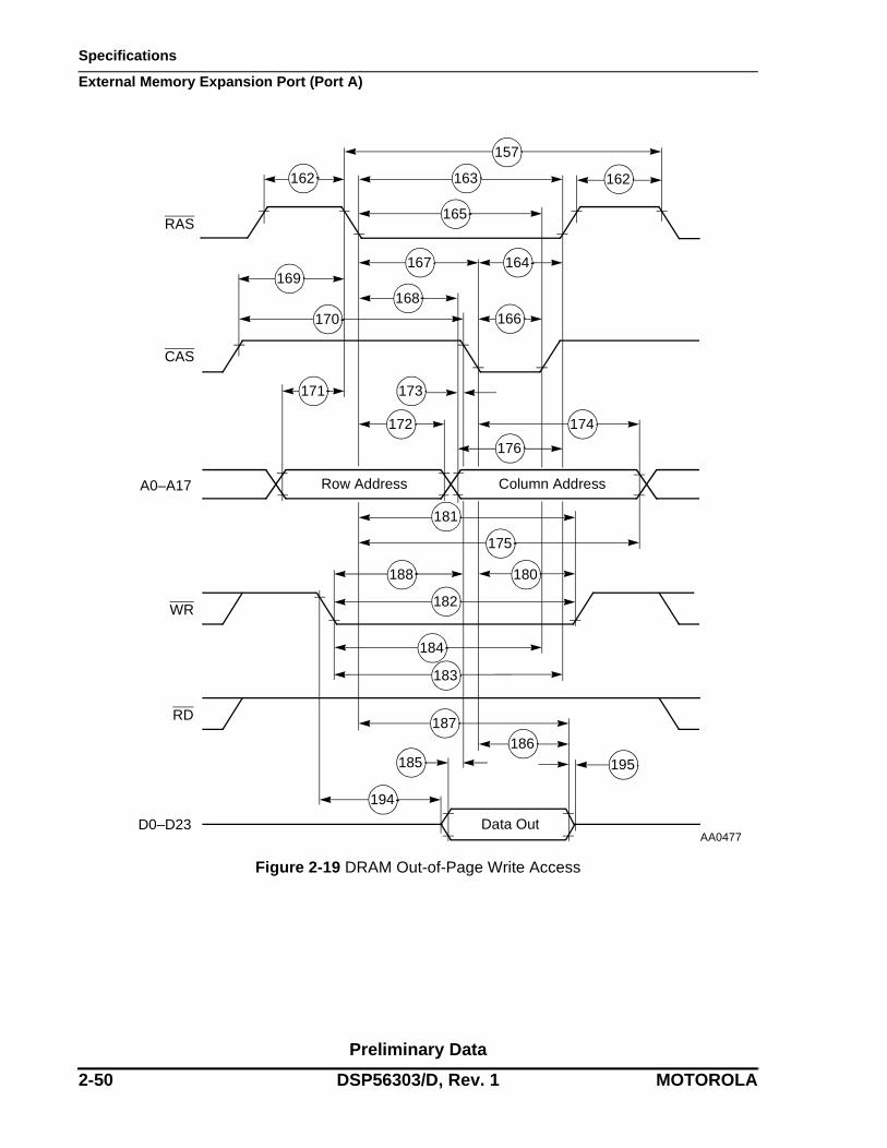
Preliminary Data
2-50 DSP56303/D, Rev. 1 MOTOROLA
Specifications
External Memory Expansion Port (Port A)
Figure 2-19 DRAM Out-of-Page Write Access
RAS
CAS
A0–A17
WR
RD
D0–D23 Data Out
Column AddressRow Address
162 163
165
162
157
169
170
167
168
164
166
171 173
174
176
172
181
175
180188
182
184
183
187
185
194
186
195
AA0477

Specifications
External Memory Expansion Port (Port A)
Preliminary Data
MOTOROLA DSP56303/D, Rev. 1 2-51
Figure 2-20 DRAM Refresh Access
RAS
CAS
WR
157
163 162162
190
170 165
189
177
AA0478
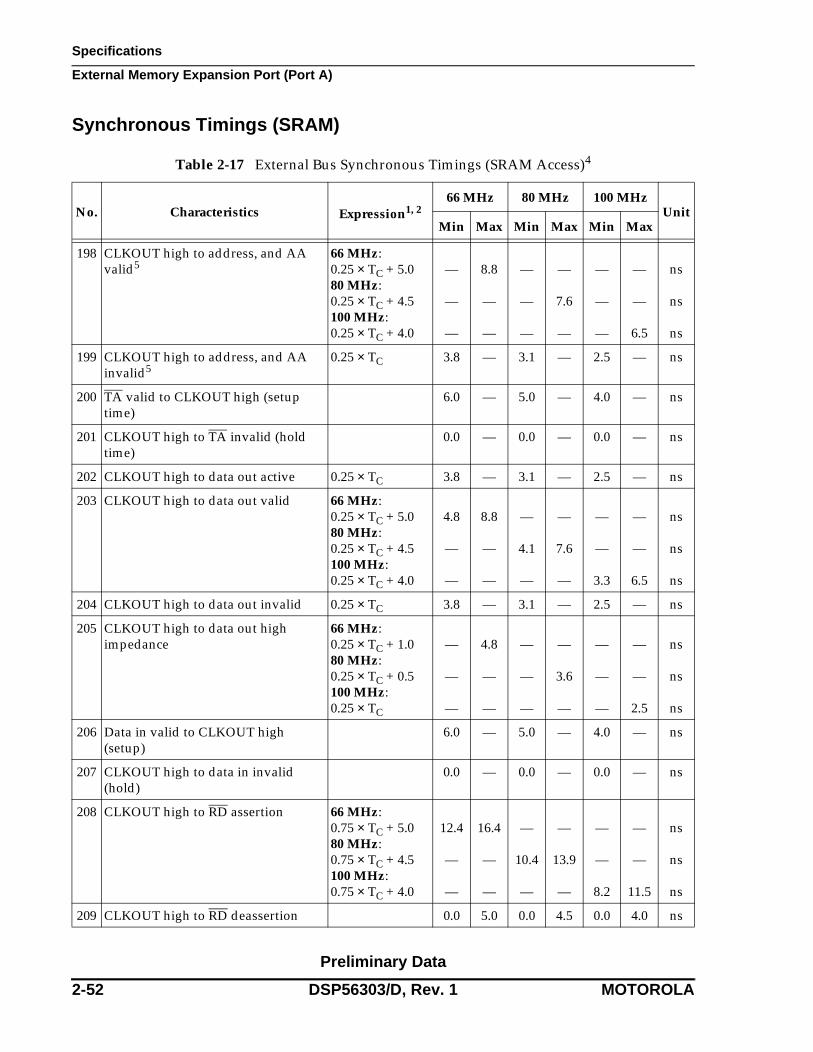
Preliminary Data
2-52 DSP56303/D, Rev. 1 MOTOROLA
Specifications
External Memory Expansion Port (Port A)
Synchronous Timings (SRAM)
Table 2-17 External Bus Synchronous Timings (SRAM Access)4
No. Characteristics Expression1, 266 MHz 80 MHz 100 MHz
Unit Min Max Min Max Min Max
198 CLKOUT high to address, and AA valid5
66 MHz:0.25 × TC + 5.080 MHz:0.25 × TC + 4.5100 MHz:0.25 × TC + 4.0
—
—
—
8.8
—
—
—
—
—
—
7.6
—
—
—
—
—
—
6.5
ns
ns
ns
199 CLKOUT high to address, and AA invalid5
0.25 × TC 3.8 — 3.1 — 2.5 — ns
200 TA valid to CLKOUT high (setup time)
6.0 — 5.0 — 4.0 — ns
201 CLKOUT high to TA invalid (hold time)
0.0 — 0.0 — 0.0 — ns
202 CLKOUT high to data out active 0.25 × TC 3.8 — 3.1 — 2.5 — ns
203 CLKOUT high to data out valid 66 MHz:0.25 × TC + 5.080 MHz:0.25 × TC + 4.5100 MHz:0.25 × TC + 4.0
4.8
—
—
8.8
—
—
—
4.1
—
—
7.6
—
—
—
3.3
—
—
6.5
ns
ns
ns
204 CLKOUT high to data out invalid 0.25 × TC 3.8 — 3.1 — 2.5 — ns
205 CLKOUT high to data out high impedance
66 MHz:0.25 × TC + 1.080 MHz:0.25 × TC + 0.5100 MHz:0.25 × TC
—
—
—
4.8
—
—
—
—
—
—
3.6
—
—
—
—
—
—
2.5
ns
ns
ns
206 Data in valid to CLKOUT high (setup)
6.0 — 5.0 — 4.0 — ns
207 CLKOUT high to data in invalid (hold)
0.0 — 0.0 — 0.0 — ns
208 CLKOUT high to RD assertion 66 MHz:0.75 × TC + 5.080 MHz:0.75 × TC + 4.5100 MHz:0.75 × TC + 4.0
12.4
—
—
16.4
—
—
—
10.4
—
—
13.9
—
—
—
8.2
—
—
11.5
ns
ns
ns
209 CLKOUT high to RD deassertion 0.0 5.0 0.0 4.5 0.0 4.0 ns

Specifications
External Memory Expansion Port (Port A)
Preliminary Data
MOTOROLA DSP56303/D, Rev. 1 2-53
210 CLKOUT high to WR assertion3 66 MHz:0.5 × TC + 5.3[WS = 1 or WS ≥ 4]80 MHz:0.5 × TC + 4.8[WS = 1 or WS ≥ 4]100 MHz:0.5 × TC + 4.3[WS = 1 or WS ≥ 4]All frequencies:[2 ≤ WS ≤ 3]
8.9
—
—
1.3
12.9
—
—
5.3
—
7.6
—
1.3
—
11.1
—
4.8
—
—
6.3
1.3
—
—
9.3
4.3
ns
ns
ns
ns
211 CLKOUT high to WR deassertion 0.0 4.8 0.0 4.3 0.0 3.8 ns
Notes: 1. WS is the number of wait states specified in the BCR.2. The asynchronous delays specified in the expressions are valid for DSP56303.3. If WS > 1, WR assertion refers to the next rising edge of CLKOUT.4. External bus synchronous timings should be used only for reference to the clock and not for relative
timings.5. T198 and T199 are valid for Address Trace mode if the ATE bit in the OMR is set. Use the status of BR
(See T212) to determine whether the access referenced by A0–A23 is internal or external, when this mode is enabled
Table 2-17 External Bus Synchronous Timings (SRAM Access)4 (Continued)
No. Characteristics Expression1, 266 MHz 80 MHz 100 MHz
Unit Min Max Min Max Min Max
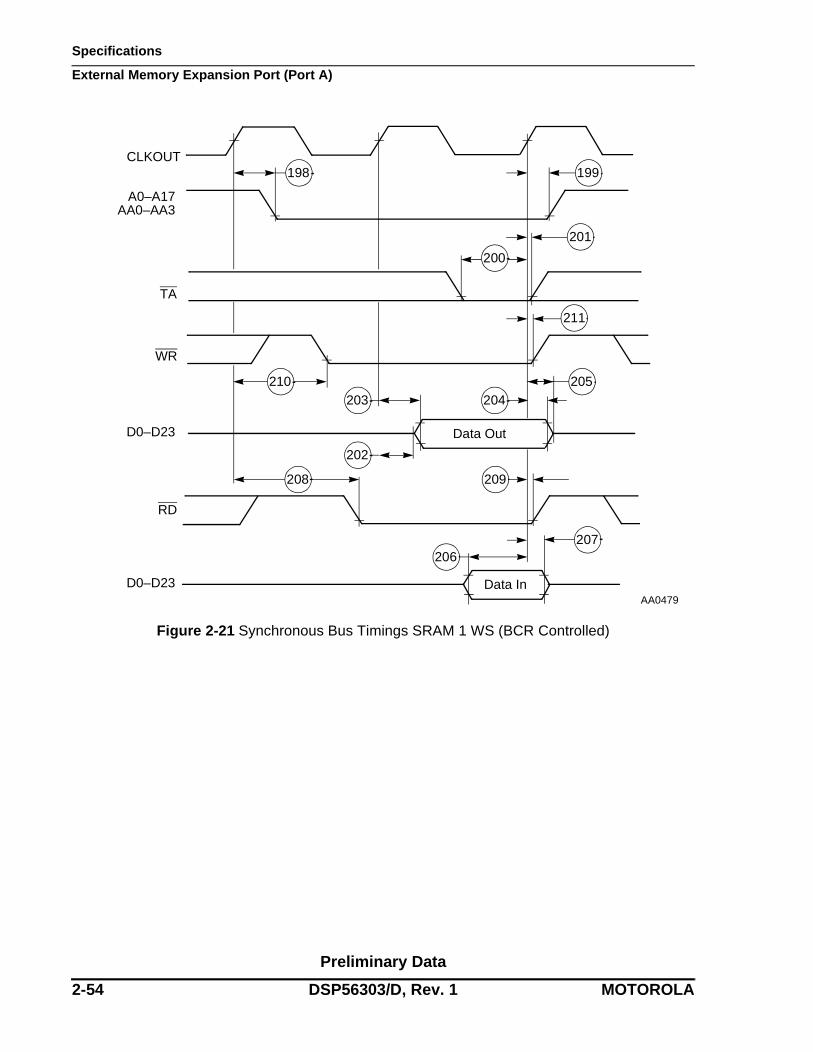
Preliminary Data
2-54 DSP56303/D, Rev. 1 MOTOROLA
Specifications
External Memory Expansion Port (Port A)
Figure 2-21 Synchronous Bus Timings SRAM 1 WS (BCR Controlled)
WR
RD
Data OutD0–D23
CLKOUT
TA
Data InD0–D23
A0–A17AA0–AA3
199
201
200
211
210
208 209
207
198
205204203
202
206
AA0479

Specifications
External Memory Expansion Port (Port A)
Preliminary Data
MOTOROLA DSP56303/D, Rev. 1 2-55
Figure 2-22 Synchronous Bus Timings SRAM 2 WS (TA Controlled)
A0–A17
WR
RD
Data OutD0–D23
AA0–AA3
CLKOUT
TA
Data InD0–D23
198 199
201200
201
211
209
207
208
210
200
203
202
205
204
206
AA0480

Preliminary Data
2-56 DSP56303/D, Rev. 1 MOTOROLA
Specifications
External Memory Expansion Port (Port A)
Arbitration Timings
Table 2-18 Arbitration Bus Timings1
No. Characteristics Expression66 MHz 80 MHz 100 MHz
Unit Min Max Min Max Min Max
212 CLKOUT high to BR assertion/deassertion2
1.0 5.0 1.0 4.5 1.0 4.0 ns
213 BG asserted/deasserted to CLKOUT high (setup)
6.0 — 5.0 — 4.0 — ns
214 CLKOUT high to BG deasserted/asserted (hold)
0.0 — 0.0 — 0.0 — ns
215 BB deassertion to CLKOUT high (input setup)
6.0 — 5.0 — 4.0 — ns
216 CLKOUT high to BB assertion (input hold)
0.0 — 0.0 — 0.0 — ns
217 CLKOUT high to BB assertion (output) 1.0 5.0 1.0 4.5 1.0 4.0 ns
218 CLKOUT high to BB deassertion (output)
1.0 5.0 1.0 4.5 1.0 4.0 ns
219 BB high to BB high impedance (output)
— 6.8 — 5.6 — 4.5 ns
220 CLKOUT high to address and controls active
0.25 × TC 3.8 — 3.1 — 2.5 — ns
221 CLKOUT high to address and controls high impedance
66 MHz:0.25 × TC + 1.080 MHz:0.25 × TC + 0.5100 MHz:0.25 × TC
—
—
—
4.8
—
—
—
—
—
—
3.6
—
—
—
—
—
—
2.5
ns
ns
ns
222 CLKOUT high to AA active 0.25 × TC 3.8 — 3.1 — 2.5 — ns
223 CLKOUT high to AA deassertion 66 MHz:0.25 × TC + 5.080 MHz:0.25 × TC + 4.5100 MHz:0.25 × TC + 4.0
4.8
—
—
8.8
—
—
—
4.1
—
—
7.6
—
—
—
3.2
—
—
6.5
ns
ns
ns
224 CLKOUT high to AA high impedance 66 MHz:0.75 × TC + 1.080 MHz:0.75 × TC + 0.5100 MHz:0.75 × TC
—
—
—
12.4
—
—
—
—
—
—
9.9
—
—
—
—
—
—
7.5
ns
ns
ns
Notes: 1. The asynchronous delays specified in the expressions are valid for DSP56303.2. T212 is valid for Address Trace mode when the ATE bit in the OMR is set. BR is deasserted for internal
accesses and asserted for external accesses.

Specifications
External Memory Expansion Port (Port A)
Preliminary Data
MOTOROLA DSP56303/D, Rev. 1 2-57
Figure 2-23 Bus Acquisition Timings
A0–A17
BB
AA0–AA3
CLKOUT
BR
BG
RD, WR
212
214
216
215
220
217
213
222
AA0481

Preliminary Data
2-58 DSP56303/D, Rev. 1 MOTOROLA
Specifications
External Memory Expansion Port (Port A)
Figure 2-24 Bus Release Timings Case 1 (BRT Bit in OMR Cleared)
A0–A17
BB
AA0–AA3
CLKOUT
BR
BG
RD, WR
212
214
218
221
224
223
213
219
AA0482

Specifications
External Memory Expansion Port (Port A)
Preliminary Data
MOTOROLA DSP56303/D, Rev. 1 2-59
Figure 2-25 Bus Release Timings Case 2 (BRT Bit in OMR Set)
A0–A17
BB
AA0–AA3
CLKOUT
BR
BG
RD, WR
223
218219
214
212
213
221
224
AA0483
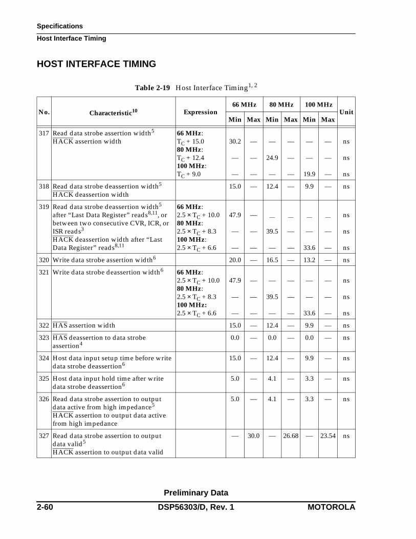
Preliminary Data
2-60 DSP56303/D, Rev. 1 MOTOROLA
Specifications
Host Interface Timing
HOST INTERFACE TIMING
Table 2-19 Host Interface Timing1, 2
No. Characteristic10 Expression66 MHz 80 MHz 100 MHz
UnitMin Max Min Max Min Max
317 Read data strobe assertion width5 HACK assertion width
66 MHz:TC + 15.080 MHz:TC + 12.4100 MHz:TC + 9.0
30.2
—
—
—
—
—
—
24.9
—
—
—
—
—
—
19.9
—
—
—
ns
ns
ns
318 Read data strobe deassertion width5 HACK deassertion width
15.0 — 12.4 — 9.9 — ns
319 Read data strobe deassertion width5 after “Last Data Register” reads8,11, or between two consecutive CVR, ICR, or ISR reads3
HACK deassertion width after “Last Data Register” reads8,11
66 MHz:2.5 × TC + 10.080 MHz:2.5 × TC + 8.3100 MHz:2.5 × TC + 6.6
47.9
—
—
—
—
—
—
39.5
—
—
—
—
—
—
33.6
—
—
—
ns
ns
ns
320 Write data strobe assertion width6 20.0 — 16.5 — 13.2 — ns
321 Write data strobe deassertion width6 66 MHz:2.5 × TC + 10.080 MHz:2.5 × TC + 8.3100 MHz:2.5 × TC + 6.6
47.9
—
—
—
—
—
—
39.5
—
—
—
—
—
—
33.6
—
—
—
ns
ns
ns
322 HAS assertion width 15.0 — 12.4 — 9.9 — ns
323 HAS deassertion to data strobe assertion4
0.0 — 0.0 — 0.0 — ns
324 Host data input setup time before write data strobe deassertion6
15.0 — 12.4 — 9.9 — ns
325 Host data input hold time after write data strobe deassertion6
5.0 — 4.1 — 3.3 — ns
326 Read data strobe assertion to output data active from high impedance5
HACK assertion to output data active from high impedance
5.0 — 4.1 — 3.3 — ns
327 Read data strobe assertion to output data valid5 HACK assertion to output data valid
— 30.0 — 26.68 — 23.54 ns

Specifications
Host Interface Timing
Preliminary Data
MOTOROLA DSP56303/D, Rev. 1 2-61
328 Read data strobe deassertion to output data high impedance5 HACK deassertion to output data high impedance
— 15.0 — 12.4 — 9.9 ns
329 Output data hold time after read data strobe deassertion5 Output data hold time after HACK deassertion
5.0 — 4.1 — 4.1 — ns
330 HCS assertion to read data strobe deassertion5
66 MHz:TC + 15.080 MHz:TC + 12.4100 MHz:TC + 9.9
30.2
—
—
—
—
—
—
24.9
—
—
—
—
—
—
19.9
—
—
—
ns
ns
ns
331 HCS assertion to write data strobe deassertion6
15.0 — 12.4 — 9.9 — ns
332 HCS assertion to output data valid — 25.0 — 20.6 — 16.5 ns
333 HCS hold time after data strobe deassertion4
0.0 — 0.0 — 0.0 — ns
334 Address (AD7–AD0) setup time before HAS deassertion (HMUX=1)
7.0 — 5.8 — 4.7 — ns
335 Address (AD7–AD0) hold time after HAS deassertion (HMUX=1)
5.0 — 4.1 — 3.3 — ns
336 A10–A8 (HMUX=1), A2–A0 (HMUX=0), HR/W setup time before data strobe assertion4
• Read• Write
07.0
——
05.8
——
04.7
——
nsns
337 A10–A8 (HMUX=1), A2–A0 (HMUX=0), HR/W hold time after data strobe deassertion4
5.0 — 4.1 — 3.3 — ns
338 Delay from read data strobe deassertion to host request assertion for “Last Data Register” read5, 7, 8
66 MHz:2 × TC + 25.080 MHz:2 × TC + 20.6100 MHz:2 × TC + 20.6
55.3
—
—
—
—
—
—
45.6
—
—
—
—
—
—
36.5
—
—
—
ns
ns
ns
Table 2-19 Host Interface Timing1, 2 (Continued)
No. Characteristic10 Expression66 MHz 80 MHz 100 MHz
UnitMin Max Min Max Min Max

Preliminary Data
2-62 DSP56303/D, Rev. 1 MOTOROLA
Specifications
Host Interface Timing
339 Delay from write data strobe deassertion to host request assertion for “Last Data Register” write6, 7, 8
66 MHz:1.5 × TC + 25.080 MHz:1.5 × TC + 20.6100 MHz:1.5 × TC + 16.5
47.7
—
—
—
—
—
—
39.4
—
—
—
—
—
—
31.5
—
—
—
ns
ns
ns
340 Delay from data strobe assertion to host request deassertion for “Last Data Register” read or write (HROD=0)4, 7, 8
— 25.0 — 22.55 — 20.24 ns
341 Delay from data strobe assertion to host request deassertion for “Last Data Register” read or write (HROD=1, open drain host request)4, 7, 8, 9
— 300.0 — 300.0 — 300.0 ns
Notes: 1. See Host Port Usage Considerations on page 1-11.2. In the timing diagrams below, the controls pins are drawn as active low. The pin polarity is
programmable.3. This timing is applicable only if two consecutive reads from one of these registers are executed.4. The data strobe is Host Read (HRD) or Host Write (HWR) in the Dual Data Strobe mode and Host Data
Strobe (HDS) in the Single Data Strobe mode.5. The read data strobe is HRD in the Dual Data Strobe mode and HDS in the Single Data Strobe mode.6. The write data strobe is HWR in the Dual Data Strobe mode and HDS in the Single Data Strobe mode.7. The host request is HREQ in the Single Host Request mode and HRRQ and HTRQ in the Double Host
Request mode.8. The “Last Data Register” is the register at address $7, which is the last location to be read or written in
data transfers. This is RXL/TXL in the Little Endian mode (HBE = 0), or RXH/TXH in the Big Endian mode (HBE = 1).
9. In this calculation, the host request signal is pulled up by a 4.7 kΩ resistor in the Open-drain mode.10. VCC = 3.3 V ± 0.3 V; TJ = −40°C to +100 °C, CL = 50 pF + 2 TTL loads11. This timing is applicable only if a read from the “Last Data Register” is followed by a read from the
RXL, RXM, or RXH registers without first polling RXDF or HREQ bits, or waiting for the assertion of the HREQ signal.
Table 2-19 Host Interface Timing1, 2 (Continued)
No. Characteristic10 Expression66 MHz 80 MHz 100 MHz
UnitMin Max Min Max Min Max

Specifications
Host Interface Timing
Preliminary Data
MOTOROLA DSP56303/D, Rev. 1 2-63
Figure 2-26 Host Interrupt Vector Register (IVR) Read Timing Diagram
Figure 2-27 Read Timing Diagram, Non-Multiplexed Bus
HACK
HD7–HD0
HREQ
329
317 318
328
326
327
AA1105
HRD, HDS
HA0–HA7
HCS
HD0–HD7
HREQ,
327
332 319
318
317
300
330
329
337336
328
326
338
341
340
333
AA0484
HRRQ,HTRQ

Preliminary Data
2-64 DSP56303/D, Rev. 1 MOTOROLA
Specifications
Host Interface Timing
Figure 2-28 Write Timing Diagram, Non-Multiplexed Bus
HWR, HDS
HA0–HA7
HCS
HD0–HD7
HREQ, HRRQ, HTRQ
336331
337
321
300
320
324325
339340
341
333
AA0485

Specifications
Host Interface Timing
Preliminary Data
MOTOROLA DSP56303/D, Rev. 1 2-65
Figure 2-29 Read Timing Diagram, Multiplexed Bus
HRD, HDS
HA8–HA10
HAS
HAD0–HAD7
HREQ, HRRQ, HTRQ
Address Data
300
317
318
319328
329
327
326
335
336 337
334
341
340 338
323
AA0486
322

Preliminary Data
2-66 DSP56303/D, Rev. 1 MOTOROLA
Specifications
Host Interface Timing
Figure 2-30 Write Timing Diagram, Multiplexed Bus
HWR, HDS
HA8–HA10
HREQ, HRRQ, HTRQ
HAS
HAD0–HAD7 Address Data
300320
321
325
324
335
341
339
336
334
340
322
323
AA0487

Specifications
SCI Timing
Preliminary Data
MOTOROLA DSP56303/D, Rev. 1 2-67
SCI TIMING
Table 2-20 SCI Timing
No. Characteristics1 Symbol Expression66 MHz 80 MHz 100 MHz
Unit Min Max Min Max Min Max
400 Synchronous clock cycle
tSCC2 8 × TC 121.0 — 100.0 — 80.0 — ns
401 Clock low period tSCC/2 − 10.0 50.5 — 40.0 — 30.0 — ns
402 Clock high period tSCC/2 − 10.0 50.5 — 40.0 — 30.0 — ns
403 Output data setup to clock falling edge (internal clock)
tSCC/4 + 0.5 × TC −17.0 20.5 — 14.3 — 8.0 — ns
404 Output data hold after clock rising edge (internal clock)
tSCC/4 − 0.5 × TC 22.5 — 18.8 — 15.0 — ns
405 Input data setup time before clock rising edge (internal clock)
tSCC/4 + 0.5 × TC + 25.0 63.0 — 56.3 — 50.0 — ns
406 Input data not valid before clock rising edge (internal clock)
tSCC/4 + 0.5 × TC − 5.5 — 32.0 — 25.8 — 19.5 ns
407 Clock falling edge to output data valid (external clock)
— 32.0 — 32.0 — 32.0 ns
408 Output data hold after clock rising edge (external clock)
TC + 8.0 23.0 — 20.5 — 18.0 — ns
409 Input data setup time before clock rising edge (external clock)
0.0 — 0.0 — 0.0 — ns
410 Input data hold time after clock rising edge (external clock)
9.0 — 9.0 — 9.0 — ns
411 Asynchronous clock cycle
tACC3 64 × TC 969.7 — 800.0 — 640.0 — ns
412 Clock low period tACC/2 − 10.0 474.8 — 390.0 — 310.0 — ns
413 Clock high period tACC/2 − 10.0 474.8 — 390.0 — 310.0 — ns

Preliminary Data
2-68 DSP56303/D, Rev. 1 MOTOROLA
Specifications
SCI Timing
414 Output data setup to clock rising edge (internal clock)
tACC/2 − 30.0 458.8 — 370.0 — 290.0 — ns
415 Output data hold after clock rising edge (internal clock)
tACC/2 − 30.0 458.8 — 370.0 — 290.0 — ns
Notes: 1. VCC = 3.3 V ± 0.3 V; TJ = −40°C to +100 °C, CL = 50 pF + 2 TTL Loads2. tSCC = synchronous clock cycle time (For internal clock, tSCC is determined by the SCI clock control
register and TC.)3. tACC = asynchronous clock cycle time; value given for 1X Clock mode (For internal clock, tACC is
determined by the SCI clock control register and TC.)
Table 2-20 SCI Timing (Continued)
No. Characteristics1 Symbol Expression66 MHz 80 MHz 100 MHz
Unit Min Max Min Max Min Max

Specifications
SCI Timing
Preliminary Data
MOTOROLA DSP56303/D, Rev. 1 2-69
Figure 2-31 SCI Synchronous Mode Timing
Figure 2-32 SCI Asynchronous Mode Timing
a) Internal Clock
Data Valid
DataValid
b) External Clock
Data Valid
SCLK(Output)
TXD
RXD
SCLK(Input)
TXD
RXD
Data Valid
400
402
404
401
403
405
406
400
402401
407
409 410
408
AA0488
1X SCLK(Output)
TXD Data Valid
413
411
412
414 415
AA0489

Preliminary Data
2-70 DSP56303/D, Rev. 1 MOTOROLA
Specifications
ESSI0/ESSI1 Timing
ESSI0/ESSI1 TIMING
Table 2-21 ESSI Timings
No. Characteristics4, 6, 7 Symbol Expression66 MHz 80 MHz 100 MHz Cond-
ition5 Unit Min Max Min Max Min Max
430 Clock cycle1 tSSICC 4 × TC3 × TC
60.645.5
——
50.037.5
——
40.030.0
——
i ckx ck
ns
431 Clock high period• For internal clock • For external clock
2 × TC − 10.01.5 × TC
20.322.7
——
15.018.8
——
10.015.0
——
nsns
432 Clock low period • For internal clock• For external clock
2 × TC − 10.01.5 × TC
20.322.7
——
15.018.8
——
10.015.0
——
nsns
433 RXC rising edge to FSR out (bl) high
——
37.022.0
——
37.022.0
——
37.022.0
x cki ck a
ns
434 RXC rising edge to FSR out (bl) low
——
37.022.0
——
37.022.0
——
37.022.0
x cki ck a
ns
435 RXC rising edge to FSR out (wr) high2
——
39.024.0
——
39.024.0
——
39.024.0
x cki ck a
ns
436 RXC rising edge to FSR out (wr) low2
——
39.024.0
——
39.024.0
——
39.024.0
x cki ck a
ns
437 RXC rising edge to FSR out (wl) high
——
36.021.0
——
36.021.0
——
36.021.0
x cki ck a
ns
438 RXC rising edge to FSR out (wl) low
——
37.022.0
——
37.022.0
——
37.022.0
x cki ck a
ns
439 Data in setup time before RXC (SCK in Synchronous mode) falling edge
0.019.0
——
0.019.0
——
0.019.0
——
x cki ck
ns
440 Data in hold time after RXC falling edge
5.03.0
——
5.03.0
——
5.03.0
——
x cki ck
ns
441 FSR input (bl, wr) high before RXC falling edge2
23.01.0
——
23.01.0
——
23.01.0
——
x cki ck a
ns
442 FSR input (wl) high before RXC falling edge
23.01.0
——
23.01.0
——
23.01.0
——
x cki ck a
ns
443 FSR input hold time after RXC falling edge
3.00.0
——
3.00.0
——
3.00.0
——
x cki ck a
ns
444 Flags input setup before RXC falling edge
0.019.0
——
0.019.0
——
0.019.0
——
x cki ck s
ns

Specifications
ESSI0/ESSI1 Timing
Preliminary Data
MOTOROLA DSP56303/D, Rev. 1 2-71
445 Flags input hold time after RXC falling edge
6.00.0
——
6.00.0
——
6.00.0
——
x cki ck s
ns
446 TXC rising edge to FST out (bl) high
——
29.015.0
——
29.015.0
——
29.015.0
x cki ck
ns
447 TXC rising edge to FST out (bl) low
——
31.017.0
——
31.017.0
——
31.017.0
x cki ck
ns
448 TXC rising edge to FST out (wr) high2
——
31.017.0
——
31.017.0
——
31.017.0
x cki ck
ns
449 TXC rising edge to FST out (wr) low2
——
33.019.0
——
33.019.0
——
33.019.0
x cki ck
ns
450 TXC rising edge to FST out (wl) high
——
30.016.0
——
30.016.0
——
30.016.0
x cki ck
ns
451 TXC rising edge to FST out (wl) low
——
31.017.0
——
31.017.0
——
31.017.0
x cki ck
ns
452 TXC rising edge to data out enable from high impedance
——
31.017.0
——
31.017.0
——
31.017.0
x cki ck
ns
453 TXC rising edge to Transmitter #0 drive enable assertion
——
34.020.0
——
34.020.0
——
34.020.0
x cki ck
ns
454 TXC rising edge to data out valid
35 + 0.5 × TC21.0
——
42.621.0
——
41.321.0
——
40.021.0
x cki ck
ns
455 TXC rising edge to data out high impedance3
——
31.016.0
——
31.016.0
——
31.016.0
x cki ck
ns
456 TXC rising edge to Transmitter #0 drive enable deassertion3
——
34.020.0
——
34.020.0
——
34.020.0
x cki ck
ns
457 FST input (bl, wr) setup time before TXC falling edge2
2.021.0
——
2.021.0
——
2.021.0
——
x cki ck
ns
458 FST input (wl) to data out enable from high impedance
— 27.0 — 27.0 — 27.0 — ns
459 FST input (wl) to Transmitter #0 drive enable assertion
— 31.0 — 31.0 — 31.0 — ns
Table 2-21 ESSI Timings (Continued)
No. Characteristics4, 6, 7 Symbol Expression66 MHz 80 MHz 100 MHz Cond-
ition5 Unit Min Max Min Max Min Max

Preliminary Data
2-72 DSP56303/D, Rev. 1 MOTOROLA
Specifications
ESSI0/ESSI1 Timing
460 FST input (wl) setup time before TXC falling edge
2.021.0
——
2.021.0
——
2.021.0
——
x cki ck
ns
461 FST input hold time after TXC falling edge
4.00.0
——
4.00.0
——
4.00.0
——
x cki ck
ns
462 Flag output valid after TXC rising edge
——
32.018.0
——
32.018.0
——
32.018.0
x cki ck
ns
Notes: 1. For the internal clock, the external clock cycle is defined by Icyc and the ESSI control register.2. The word-relative frame sync signal waveform relative to the clock operates in the same manner as the
bit-length frame sync signal waveform, but spreads from one serial clock before first bit clock (same as Bit Length Frame Sync signal), until the one before last bit clock of the first word in frame.
3. Periodically sampled and not 100% tested4. VCC = 3.3 V ± 0.3 V; TJ = −40°C to +100 °C, CL = 50 pF + 2 TTL Loads5. TXC (SCK Pin) = Transmit Clock
RXC (SC0 or SCK Pin) = Receive ClockFST (SC2 Pin) = Transmit Frame SyncFSR (SC1 or SC2 Pin) Receive Frame Sync
6. i ck = Internal Clockx ck = External Clocki ck a = Internal Clock, Asynchronous Mode
(Asynchronous implies that TXC and RXC are two different clocks)i ck s = Internal Clock, Synchronous Mode
(Synchronous implies that TXC and RXC are the same clock)7. bl = bit length
wl = word lengthwr = word length relative
Table 2-21 ESSI Timings (Continued)
No. Characteristics4, 6, 7 Symbol Expression66 MHz 80 MHz 100 MHz Cond-
ition5 Unit Min Max Min Max Min Max

Specifications
ESSI0/ESSI1 Timing
Preliminary Data
MOTOROLA DSP56303/D, Rev. 1 2-73
Figure 2-33 ESSI Transmitter Timing
Last Bit
See Note
Note: In Network mode, output flag transitions can occur at the start of each time slot within the frame. In Normal mode, the output flag state is asserted for the entire frame period.
First Bit
430
432
446 447
450 451
455
454454
452
459
456453
461
457
458
460 461
462
431
AA0490
TXC(Input/
Output)
FST (Bit)Out
FST (Word)Out
Data Out
Transmitter#0 Drive
Enable
FST (Bit) In
FST (Word)In
Flags Out

Preliminary Data
2-74 DSP56303/D, Rev. 1 MOTOROLA
Specifications
ESSI0/ESSI1 Timing
Figure 2-34 ESSI Receiver Timing
Last BitFirst Bit
430
432
433
437 438
440439
443441
442 443
445444
431
434
RXC(Input/
Output)
FSR (Bit)Out
FSR(Word)
Out
Data In
FSR (Bit)In
FSR(Word)
In
Flags In
AA0491

Specifications
Timer Timing
Preliminary Data
MOTOROLA DSP56303/D, Rev. 1 2-75
TIMER TIMING
Table 2-22 Timer Timing
No. Characteristics Expression66 MHz 80 MHz 100 MHz
Unit Min Max Min Max Min Max
480 TIO Low 2 × TC + 2.0 32.5 — 27.0 — 22.0 — ns
481 TIO High 2 × TC + 2.0 32.5 — 27.0 — 22.0 — ns
482 Timer setup time from TIO (Input) assertion to CLKOUT rising edge
9.0 15.15 9.0 12.5 9.0 10.0 ns
483 Synchronous timer delay time from CLKOUT rising edge to the external memory access address out valid caused by first interrupt instruction execution
10.25 × TC + 1.0 156.0 — 129.1 — 103.5 — ns
484 CLKOUT rising edge to TIO (Output) assertion• Minimum• Maximum
0.5 × TC + 3.50.5 × TC + 19.8
11.1—
—28.1
9.8—
—26.1
8.5—
—24.8
nsns
485 CLKOUT rising edge to TIO (Output) deassertion• Minimum• Maximum
60.5 × TC + 3.566–80 MHz:0.5 × TC + 19.8100 MHz:0.5 × TC + 19.0
11.1
—
—
—
28.1
—
9.8
—
—
—
26.1
—
8.5
—
—
—
—
24.8
ns
ns
ns
Note: VCC = 3.3 V ± 0.3 V; TJ = −40°C to +100 °C, CL = 50 pF + 2 TTL Loads
Figure 2-35 TIO Timer Event Input Restrictions
TIO
481480AA0492

Preliminary Data
2-76 DSP56303/D, Rev. 1 MOTOROLA
Specifications
Timer Timing
Figure 2-36 Timer Interrupt Generation
Figure 2-37 External Pulse Generation
CLKOUT
TIO (Input)
First Interrupt Instruction Execution
Address
482
483
AA0493
CLKOUT
TIO (Output)
484 485AA0494

Specifications
GPIO Timing
Preliminary Data
MOTOROLA DSP56303/D, Rev. 1 2-77
GPIO TIMING
Table 2-23 GPIO Timing
No. Characteristics Expression66 MHz 80 MHz 100 MHz
Unit Min Max Min Max Min Max
490 CLKOUT edge to GPIO out valid (GPIO out delay time)
— 31.0 — 31.0 — 31.0 ns
491 CLKOUT edge to GPIO out not valid (GPIO out hold time)
3.0 — 3.0 — 3.0 — ns
492 GPIO In valid to CLKOUT edge (GPIO in set-up time)
12.0 — 12.0 — 12.0 — ns
493 CLKOUT edge to GPIO in not valid (GPIO in hold time)
0.0 — 0.0 — 0.0 — ns
494 Fetch to CLKOUT edge before GPIO change
6.75 × TC 102.3 — 84.4 — 67.5 — ns
Note: VCC = 3.3 V ± 0.3 V; TJ = −40°C to +100 °C, CL = 50 pF + 2 TTL Loads
Figure 2-38 GPIO Timing
ValidGPIO(Input)
GPIO (Output)
CLKOUT(Output)
Fetch the instruction MOVE X0,X:(R0); X0 contains the new value of GPIOand R0 contains the address of GPIO data register.
A0–A17
490
491
492
494
493
AA0495

Preliminary Data
2-78 DSP56303/D, Rev. 1 MOTOROLA
Specifications
JTAG Timing
JTAG TIMING
Table 2-24 JTAG Timing
No. CharacteristicsAll frequencies
Unit Min Max
500 TCK frequency of operation (1/(TC
× 3); maximum 22 MHz) 0.0 22.0 MHz
501 TCK cycle time in Crystal mode 45.0 — ns
502 TCK clock pulse width measured at 1.5 V 20.0 — ns
503 TCK rise and fall times 0.0 3.0 ns
504 Boundary scan input data setup time 5.0 — ns
505 Boundary scan input data hold time 24.0 — ns
506 TCK low to output data valid 0.0 40.0 ns
507 TCK low to output high impedance 0.0 40.0 ns
508 TMS, TDI data setup time 5.0 — ns
509 TMS, TDI data hold time 25.0 — ns
510 TCK low to TDO data valid 0.0 44.0 ns
511 TCK low to TDO high impedance 0.0 44.0 ns
512 TRST assert time 100.0 — ns
513 TRST setup time to TCK low 40.0 — ns
Notes: 1. VCC = 3.3 V ± 0.3 V; TJ = −40°C to +100 °C, CL = 50 pF + 2 TTL Loads2. All timings apply to OnCE module data transfers because it uses the JTAG port as an interface.
Figure 2-39 Test Clock Input Timing Diagram
TCK(Input)
VM VMVIHVIL
501
502 502
503503AA0496

Specifications
JTAG Timing
Preliminary Data
MOTOROLA DSP56303/D, Rev. 1 2-79
Figure 2-40 Boundary Scan (JTAG) Timing Diagram
Figure 2-41 Test Access Port Timing Diagram
TCK(Input)
DataInputs
DataOutputs
DataOutputs
DataOutputs
VIHVIL
Input Data Valid
Output Data Valid
Output Data Valid
505504
506
507
506
AA0497
TCK(Input)
TDI
(Input)
TDO(Output)
TDO(Output)
TDO(Output)
VIHVIL
Input Data Valid
Output Data Valid
Output Data Valid
TMS
508 509
510
511
510
AA0498
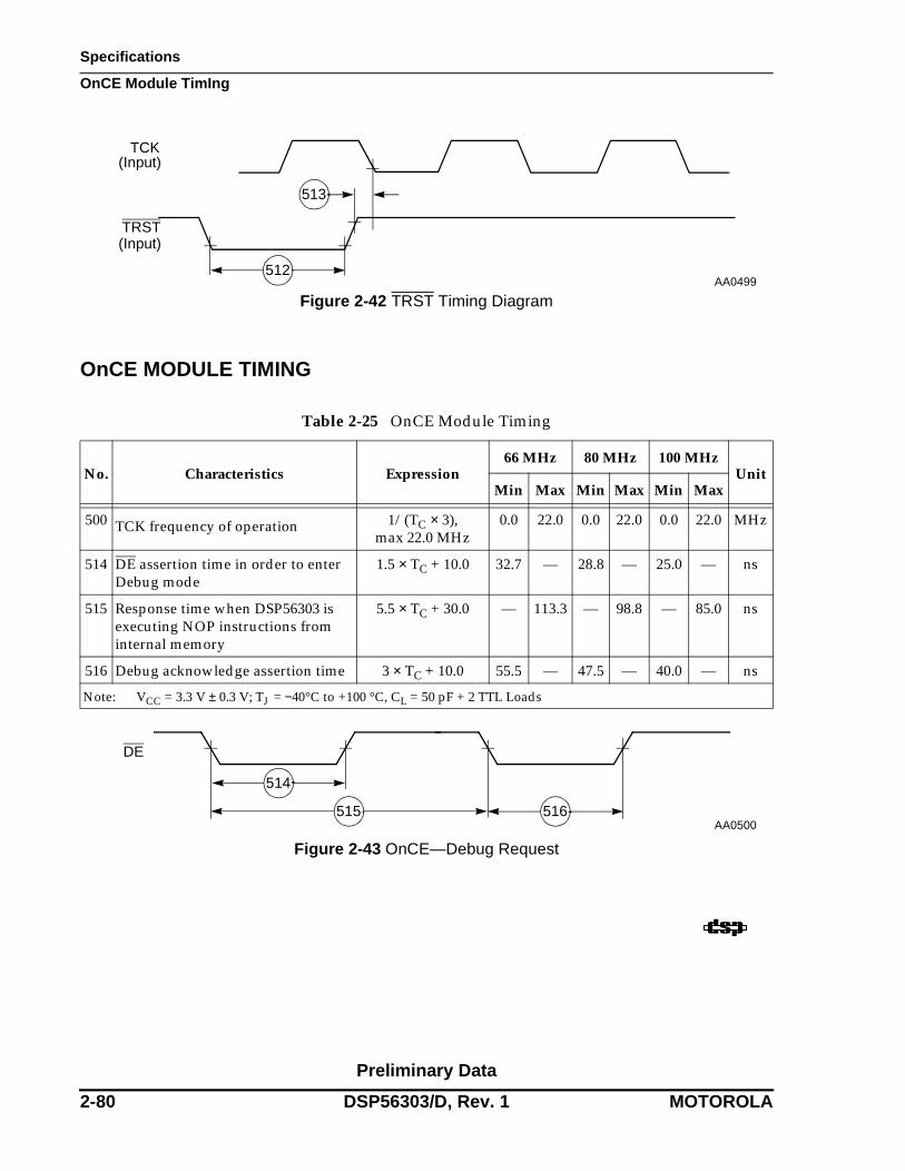
Preliminary Data
2-80 DSP56303/D, Rev. 1 MOTOROLA
Specifications
OnCE Module TimIng
OnCE MODULE TIMING
Figure 2-42 TRST Timing Diagram
Table 2-25 OnCE Module Timing
No. Characteristics Expression66 MHz 80 MHz 100 MHz
Unit Min Max Min Max Min Max
500 TCK frequency of operation 1/(TC × 3), max 22.0 MHz
0.0 22.0 0.0 22.0 0.0 22.0 MHz
514 DE assertion time in order to enter Debug mode
1.5 × TC + 10.0 32.7 — 28.8 — 25.0 — ns
515 Response time when DSP56303 is executing NOP instructions from internal memory
5.5 × TC + 30.0 — 113.3 — 98.8 — 85.0 ns
516 Debug acknowledge assertion time 3 × TC + 10.0 55.5 — 47.5 — 40.0 — ns
Note: VCC = 3.3 V ± 0.3 V; TJ = −40°C to +100 °C, CL = 50 pF + 2 TTL Loads
Figure 2-43 OnCE—Debug Request
TCK(Input)
TRST(Input)
513
512AA0499
DE
516515
514
AA0500

Preliminary Data
MOTOROLA DSP56303/D, Rev. 1 3-1
SECTION 3
PACKAGING
PIN-OUT AND PACKAGE INFORMATION
This sections provides information about the available packages for this product, including diagrams of the package pinouts and tables describing how the signals described in Section 1 are allocated for each package.
The DSP56303 is available in two package types:
• 144-pin Thin Quad Flat Pack (TQFP)
• 196-pin Plastic Ball Grid Array (PBGA)

Preliminary Data
3-2 DSP56303/D, Rev. 1 MOTOROLA
Packaging
Pin-out and Package Information
TQFP Package Description
Top and bottom views of the TQFP package are shown in Figure 3-1 and Figure 3-2 with their pin-outs.
Figure 3-1 DSP56303 Thin Quad Flat Pack (TQFP), Top View
SR
D1
ST
D1
SC
02S
C01 D
EP
INIT
SR
D0
VC
CS
GN
DS
ST
D0
SC
10S
C00
RX
DT
XD
SC
LKS
CK
1S
CK
0V
CC
QG
ND
QN
CH
DS
HR
WH
AC
KH
RE
QV
CC
SG
ND
ST
IO2
TIO
1T
IO0
HC
SH
A9
HA
8H
AS
HA
D7
HA
D6
HA
D5
HAD4VCCH
GNDH
HAD3HAD2HAD1HAD0RESETVCCP
PCAPGNDP
GNDP1
NCAA3AA2CASXTALGNDQ
EXTALVCCQ
VCCC
GNDC
CLKOUTBCLKBCLKTABRBBVCCC
GNDC
WRRDAA1AA0BGA0D7
D8VCCD
GNDDD9
D10D11D12D13D14
VCCDGNDD
D15D16D17D18D19
VCCQGNDQ
D20VCCD
GNDDD21D22D23
TRSTTDOTDI
TCKTMS
SC12SC11 1 37
73109 (Top View)
Orientation Mark
A1
VC
CA
GN
DA
A2
A3
A4
A5
VC
CA
GN
DA
A6
A7
A8
A9
VC
CA
GN
DA
A10
A11
GN
DQ
VC
CQ
A12
A13
A14
VC
CA
GN
DA
A15
A16
A17
D0
D1
D2
VC
CD
GN
DD
D3
D4
D5
D6
AA0301
MODDMODCMODBMODA
Note: Because of size constraints in this figure, only one name is shown for multiplexed pins. Refer to Table 3-1 and Table 3-2 for detailed information about pin functions and signal names.

Packaging
Pin-out and Package Information
Preliminary Data
MOTOROLA DSP56303/D, Rev. 1 3-3
Figure 3-2 DSP56303 Thin Quad Flat Pack (TQFP), Bottom View
SR
D1
ST
D1
SC
02S
C01D
EP
INIT
SR
D0
VC
CS
GN
DS
ST
D0
SC
10S
C00
RX
DT
XD
SC
LKS
CK
1S
CK
0V
CC
Q
GN
DQ
NC
HD
SH
RW
HA
CK
HR
EQ
VC
CS
GN
DS
TIO
2T
IO1
TIO
0H
CS
HA
9H
A8
HA
SH
AD
7H
AD
6H
AD
5
HAD4VCCH
GNDH
HAD3HAD2HAD1HAD0RESET
VCCP
PCAPGNDP
GNDP1
NCAA3AA2CAS
XTALGNDQ
EXTALVCCQ
VCCC
GNDC
CLKOUTBCLKBCLK
TABRBB
VCCC
GNDC
WRRD
AA1AA0
BGA0 D7
D8VCCDGNDD
D9D10D11D12D13D14VCCDGNDD
D15D16D17D18D19VCCQGNDQ
D20VCCDGNDD
D21D22D23MODDMODCMODBMODATRSTTDOTDITCKTMSSC12SC11137
73109(Bottom View)
A1
VC
CA
GN
DA
A2
A3
A4
A5
VC
CA
GN
DA
A6
A7
A8
A9
VC
CA
GN
DA
A10
A11
GN
DQ
VC
CQ
A12
A13
A14
VC
CA
GN
DA
A15
A16
A17
D0
D1
D2
VC
CD
GN
DD
D3
D4
D5
D6
Orientation Mark(on top side)
AA0302
Note: Because of size constraints in this figure, only one name is shown for multiplexed pins. Refer to Table 3-1 and Table 3-2 for detailed information about pin functions and signal names.

Preliminary Data
3-4 DSP56303/D, Rev. 1 MOTOROLA
Packaging
Pin-out and Package Information
Table 3-1 DSP56303 TQFP Signal Identification by Pin Number
Pin No.
Signal NamePin No.
Signal NamePin No.
Signal Name
1 SRD1 or PD4 26 GNDS 51 AA2/RAS2
2 STD1 or PD5 27 TIO2 52 CAS
3 SC02 or PC2 28 TIO1 53 XTAL
4 SC01 or PC1 29 TIO0 54 GNDQ
5 DE 30 HCS/HCS, HA10, or PB13 55 EXTAL
6 PINIT/NMI 31 HA2, HA9, or PB10 56 VCCQ
7 SRD0 or PC4 32 HA1, HA8, or PB9 57 VCCC
8 VCCS 33 HA0, HAS/HAS, or PB8 58 GNDC
9 GNDS 34 H7, HAD7, or PB7 59 CLKOUT
10 STD0 or PC5 35 H6, HAD6, or PB6 60 BCLK
11 SC10 or PD0 36 H5, HAD5, or PB5 61 BCLK
12 SC00 or PC0 37 H4, HAD4, or PB4 62 TA
13 RXD or PE0 38 VCCH 63 BR
14 TXD or PE1 39 GNDH 64 BB
15 SCLK or PE2 40 H3, HAD3, or PB3 65 VCCC
16 SCK1 or PD3 41 H2, HAD2, or PB2 66 GNDC
17 SCK0 or PC3 42 H1, HAD1, or PB1 67 WR
18 VCCQ 43 H0, HAD0, or PB0 68 RD
19 GNDQ 44 RESET 69 AA1/RAS1
20 Not Connected (NC), reserved
45 VCCP 70 AA0/RAS0
21 HDS/HDS, HWR/HWR, or PB12
46 PCAP 71 BG
22 HRW, HRD/HRD, or PB11 47 GNDP 72 A0
23 HACK/HACK, HRRQ/HRRQ, or PB15
48 GNDP1 73 A1
24 HREQ/HREQ,HTRQ/HTRQ, or PB14
49 Not Connected (NC), reserved
74 VCCA
25 VCCS 50 AA3/RAS3 75 GNDA

Packaging
Pin-out and Package Information
Preliminary Data
MOTOROLA DSP56303/D, Rev. 1 3-5
76 A2 99 A17 122 D16
77 A3 100 D0 123 D17
78 A4 101 D1 124 D18
79 A5 102 D2 125 D19
80 VCCA 103 VCCD 126 VCCQ
81 GNDA 104 GNDD 127 GNDQ
82 A6 105 D3 128 D20
83 A7 106 D4 129 VCCD
84 A8 107 D5 130 GNDD
85 A9 108 D6 131 D21
86 VCCA 109 D7 132 D22
87 GNDA 110 D8 133 D23
88 A10 111 VCCD 134 MODD/IRQD
89 A11 112 GNDD 135 MODC/IRQC
90 GNDQ 113 D9 136 MODB/IRQB
91 VCCQ 114 D10 137 MODA/IRQA
92 A12 115 D11 138 TRST
93 A13 116 D12 139 TDO
94 A14 117 D13 140 TDI
95 VCCA 118 D14 141 TCK
96 GNDA 119 VCCD 142 TMS
97 A15 120 GNDD 143 SC12 or PD2
98 A16 121 D15 144 SC11 or PD1
Note: Signal names are based on configured functionality. Most pins supply a single signal. Some pins provide a signal with dual functionality, such as the MODx/IRQx pins that select an operating mode after RESET is deasserted, but act as interrupt lines during operation. Some signals have configurable polarity; these names are shown with and without overbars, such as HAS/HAS. Some pins have two or more configurable functions; names assigned to these pins indicate the function for a specific configuration. For example, Pin 34 is data line H7 in non-multiplexed bus mode, data/address line HAD7 in multiplexed bus mode, or GPIO line PB7 when the GPIO function is enabled for this pin.
Table 3-1 DSP56303 TQFP Signal Identification by Pin Number (Continued)
Pin No.
Signal NamePin No.
Signal NamePin No.
Signal Name

Preliminary Data
3-6 DSP56303/D, Rev. 1 MOTOROLA
Packaging
Pin-out and Package Information
Table 3-2 DSP56303 TQFP Signal Identification by Name
Signal NamePin No.
Signal NamePin No.
Signal NamePin No.
A0 72 BG 71 D7 109
A1 73 BR 63 D8 110
A10 88 CAS 52 D9 113
A11 89 CLKOUT 59 DE 5
A12 92 D0 100 EXTAL 55
A13 93 D1 101 GNDA 75
A14 94 D10 114 GNDA 81
A15 97 D11 115 GNDA 87
A16 98 D12 116 GNDA 96
A17 99 D13 117 GNDC 58
A2 76 D14 118 GNDC 66
A3 77 D15 121 GNDD 104
A4 78 D16 122 GNDD 112
A5 79 D17 123 GNDD 120
A6 82 D18 124 GNDD 130
A7 83 D19 125 GNDH 39
A8 84 D2 102 GNDP 47
A9 85 D20 128 GNDP1 48
AA0 70 D21 131 GNDQ 19
AA1 69 D22 132 GNDQ 54
AA2 51 D23 133 GNDQ 90
AA3 50 D3 105 GNDQ 127
BB 64 D4 106 GNDS 9
BCLK 60 D5 107 GNDS 26
BCLK 61 D6 108 H0 43
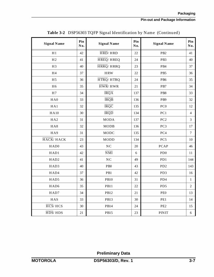
Packaging
Pin-out and Package Information
Preliminary Data
MOTOROLA DSP56303/D, Rev. 1 3-7
H1 42 HRD/HRD 22 PB2 41
H2 41 HREQ/HREQ 24 PB3 40
H3 40 HRRQ/HRRQ 23 PB4 37
H4 37 HRW 22 PB5 36
H5 36 HTRQ/HTRQ 24 PB6 35
H6 35 HWR/HWR 21 PB7 34
H7 34 IRQA 137 PB8 33
HA0 33 IRQB 136 PB9 32
HA1 32 IRQC 135 PC0 12
HA10 30 IRQD 134 PC1 4
HA2 31 MODA 137 PC2 3
HA8 32 MODB 136 PC3 17
HA9 31 MODC 135 PC4 7
HACK/HACK 23 MODD 134 PC5 10
HAD0 43 NC 20 PCAP 46
HAD1 42 NMI 6 PD0 11
HAD2 41 NC 49 PD1 144
HAD3 40 PB0 43 PD2 143
HAD4 37 PB1 42 PD3 16
HAD5 36 PB10 31 PD4 1
HAD6 35 PB11 22 PD5 2
HAD7 34 PB12 21 PE0 13
HAS 33 PB13 30 PE1 14
HCS/HCS 30 PB14 24 PE2 15
HDS/HDS 21 PB15 23 PINIT 6
Table 3-2 DSP56303 TQFP Signal Identification by Name (Continued)
Signal NamePin No.
Signal NamePin No.
Signal NamePin No.

Preliminary Data
3-8 DSP56303/D, Rev. 1 MOTOROLA
Packaging
Pin-out and Package Information
RAS0 70 SRD1 1 VCCC 57
RAS1 69 STD0 10 VCCC 65
RAS2 51 STD1 2 VCCD 103
RAS3 50 TA 62 VCCD 111
RD 68 TCK 141 VCCD 119
RESET 44 TDI 140 VCCD 129
RXD 13 TDO 139 VCCH 38
SC00 12 TIO0 29 VCCP 45
SC01 4 TIO1 28 VCCQ 18
SC02 3 TIO2 27 VCCQ 56
SC10 11 TMS 142 VCCQ 91
SC11 144 TRST 138 VCCQ 126
SC12 143 TXD 14 VCCS 8
SCK0 17 VCCA 74 VCCS 25
SCK1 16 VCCA 80 WR 67
SCLK 15 VCCA 86 XTAL 53
SRD0 7 VCCA 95
Table 3-2 DSP56303 TQFP Signal Identification by Name (Continued)
Signal NamePin No.
Signal NamePin No.
Signal NamePin No.

Packaging
Pin-out and Package Information
Preliminary Data
MOTOROLA DSP56303/D, Rev. 1 3-9
TQFP Package Mechanical Drawing
Figure 3-3 DSP56303 Mechanical Information, 144-pin TQFP Package
SEATINGPLANE
0.1 T 144XC 2θ
VIEW AB
2θT
PLATING
F AAJ
DBASEMETAL
SECTION J1-J1(ROTATED 90)
144 PL
M0.08 NT L-M
N0.20 T L-M
144
73
109
37
1081
36
72
4X 4X 36 TIPS
PIN 1 IDENT
VIEW Y
B
B1 V1
A1
S1
V
A
S
N0.20 T L-M
ML
N
P4X
G140X
J1
J1
VIEW Y
CL
XX=L, M OR N
GAGE PLANE
θ
0.05
(Z)
R2
E
C2
(Y)
R1
(K)C1
1θ
0.25
VIEW AB
DIM MIN MAXMILLIMETERS
A 20.00 BSCA1 10.00 BSCB 20.00 BSC
B1 10.00 BSCC 1.40 1.60
C1 0.05 0.15C2 1.35 1.45D 0.17 0.27E 0.45 0.75F 0.17 0.23G 0.50 BSCJ 0.09 0.20K 0.50 REFP 0.25 BSC
R1 0.13 0.20R2 0.13 0.20S 22.00 BSC
S1 11.00 BSCV 22.00 BSC
V1 11.00 BSCY 0.25 REFZ 1.00 REF
AA 0.09 0.16θ 0°
θ 0° 7°θ 11° 13°
12
NOTES:1. DIMENSIONS AND TOLERANCING PER ASME
Y14.5, 1994.2. DIMENSIONS IN MILLIMETERS.3. DATUMS L, M AND N TO BE DETERMINED AT THE
SEATING PLANE, DATUM T.4. DIMENSIONS S AND V TO BE DETERMINED AT
SEATING PLANE, DATUM T.5. DIMENSIONS A AND B DO NOT INCULDE MOLD
PROTRUSION. ALLOWABLE PROTRUSION IS 0.25 PER SIDE. DIMENSIONS A AND B DO INCLUDE MOLD MISMATCH AND ARE DETERMINED AT DATUM PLANE H.
6. DIMENSION D DOES NOT INCLUDE DAMBAR PROTRUSION. ALLOWABLED DAMBAR PROTRUSION SHALL NOT CAUSE THE D DIMENSION TO EXCEED 0.35.
CASE 918-03
—
ISSUE C

Preliminary Data
3-10 DSP56303/D, Rev. 1 MOTOROLA
Packaging
Pin-out and Package Information
PBGA Package Description
Top and bottom views of the PBGA package are shown in Figure 3-4 and Figure 3-5 with their pin-outs.
Figure 3-4 DSP56303 Plastic Ball Grid Array (PBGA), Top View
1 3 42 5 6 7 8 10 141312119
NC
HACK
HREQ
B
C
D
E
F
G
H
N
M
L
J
K
HA0
HRW HDS
HCS
MODD
H5 NC
H7
HA1 HA2
H2
VCCD
VCCQMODA
D19
D18 VCCD
VCCD
VCCQ
VCCS
VCCAGND GND GND GND GND
GND
GNDGNDGNDGND
GND
GND
GND
GND GND
GND
GND
GNDGNDGNDGND
GND GNDGND
GNDGNDGND
GND GND GND
VCCA
VCCC
VCCA
VCCA
VCCPVCCH
VCCS
VCCQ
GND
GND
GND
GND
GND
GND
VCCD
NC
MODC
H4H6 VCCQ
D12
D11
D15
D9
D5
D3
D0
A0
A17 A16
A1 A2
H1
PB0
H3
TIO1
RXD
TIO2
TIO0
SCK1 TXD
SC12
SC11
STD1
SCK0
SRD0
SRD1
STD0
SC02
SC01
TDOTMS
DE
TA
TDI
TCK
A15
A12
A7
A5
BG
GNDP
PINIT
AA0
TRST
SCLK
VCCC
P
A
Top View
MODB D23
D22
D21 D20 D17
D16 D14
D13 D10 D8
D7
D6 D4
D2D1
A14
A13
A11A10
A9A8
A6
A4A3
AA1
RDWR
BB
BR
BCLK
BCLK
CLKOUT
XTAL
CASAA3
AA2GNDP1PCAP
RESET
SC00SC10
NC
NC
NC
NC
GND GND
GND
GND GND
GND GND
GND GND
GND GND
GND
GND
GND
GND
GND
GND
GND
GND
GND
GND
GND
GND
GND
GND GND
GNDGND
EXTAL

Packaging
Pin-out and Package Information
Preliminary Data
MOTOROLA DSP56303/D, Rev. 1 3-11
Figure 3-5 DSP56303 Plastic Ball Grid Array (PBGA), Bottom View
Bottom View134 256781014 13 12 11 9
NC
HACK
HREQ
B
C
D
E
F
G
H
N
M
L
J
K
HA0
HRWHDS
HCS
MODD
H5NC
H7
HA1HA2
H2
VCCD
VCCQ MODA
D19
D18VCCD
VCCD
VCCQ
VCCS
VCCA GNDGNDGNDGNDGND
GND
GND GND GND GND
GND
GND
GND
GNDGND
GND
GND
GND GND GND GND
GNDGND GND
GND GND GND
GNDGNDGND
VCCA
VCCC
VCCA
VCCA
VCCP VCCH
VCCS
VCCQ
GND
GND
GND
GND
GND
GND
VCCD
NC
MODC
H4 H6VCCQ
D12
D11
D15
D9
D5
D3
D0
A0
A17A16
A1A2
H1
PB0
H3
TIO1
RXD
TIO2
TIO0
SCK1TXD
SC12
SC11
STD1
SCK0
SRD0
SRD1
STD0
SC02
SC01
TDO TMS
DE
TA
TDI
TCK
A15
A12
A7
A5
BG
GNDP
PINIT
AA0
TRST
SCLK
VCCC
P
AMODBD23
D22
D21D20D17
D16D14
D13D10D8
D7
D6D4
D2 D1
A14
A13
A11 A10
A9 A8
A6
A4 A3
AA1
RD WR
BB
BR
BCLK
BCLK
CLKOUT
XTAL
CAS AA3
AA2 GNDP1 PCAP
RESET
SC00 SC10
NC
NC
NC
NC
GNDGND
GND
GNDGND
GNDGND
GNDGND
GNDGND
GND
GND
GND
GND
GND
GND
GND
GND
GND
GND
GND
GND
GND
GNDGND
GND GND
EXTAL

Preliminary Data
3-12 DSP56303/D, Rev. 1 MOTOROLA
Packaging
Pin-out and Package Information
Table 3-3 DSP56303 PBGA Signal Identification by Pin Number
Pin No.
Signal NamePin No.
Signal NamePin No.
Signal Name
A1 Not Connected (NC), reserved
B12 D8 D9 GND
A2 SC11 or PD1 B13 D5 D10 GND
A3 TMS B14 NC D11 GND
A4 TDO C1 SC02 or PC2 D12 D1
A5 MODB/IRQB C2 STD1 or PD5 D13 D2
A6 D23 C3 TCK D14 VCCD
A7 VCCD C4 MODA/IRQA E1 STD0 or PC5
A8 D19 C5 MODC/IRQC E2 VCCS
A9 D16 C6 D22 E3 SRD0 or PC4
A10 D14 C7 VCCQ E4 GND
A11 D11 C8 D18 E5 GND
A12 D9 C9 VCCD E6 GND
A13 D7 C10 D12 E7 GND
A14 NC C11 VCCD E8 GND
B1 SRD1 or PD4 C12 D6 E9 GND
B2 SC12 or PD2 C13 D3 E10 GND
B3 TDI C14 D4 E11 GND
B4 TRST D1 PINIT/NMI E12 A17
B5 MODD/IRQD D2 SC01 or PC1 E13 A16
B6 D21 D3 DE E14 D0
B7 D20 D4 GND F1 RXD or PE0
B8 D17 D5 GND F2 SC10 or PD0
B9 D15 D6 GND F3 SC00 or PC0
B10 D13 D7 GND F4 GND
B11 D10 D8 GND F5 GND

Packaging
Pin-out and Package Information
Preliminary Data
MOTOROLA DSP56303/D, Rev. 1 3-13
F6 GND H3 SCK0 or PC3 J14 A9
F7 GND H4 GND K1 VCCS
F8 GND H5 GND K2 HREQ/HREQ,HTRQ/HTRQ, or PB14
F9 GND H6 GND K3 TIO2
F10 GND H7 GND K4 GND
F11 GND H8 GND K5 GND
F12 VCCA H9 GND K6 GND
F13 A14 H10 GND K7 GND
F14 A15 H11 GND K8 GND
G1 SCK1 or PD3 H12 VCCA K9 GND
G2 SCLK or PE2 H13 A10 K10 GND
G3 TXD or PE1 H14 A11 K11 GND
G4 GND J1 HACK/HACK, HRRQ/HRRQ, or PB15
K12 VCCA
G5 GND J2 HRW, HRD/HRD, or PB11 K13 A5
G6 GND J3 HDS/HDS, HWR/HWR, or PB12
K14 A6
G7 GND J4 GND L1 HCS/HCS, HA10, or PB13
G8 GND J5 GND L2 TIO1
G9 GND J6 GND L3 TIO0
G10 GND J7 GND L4 GND
G11 GND J8 GND L5 GND
G12 A13 J9 GND L6 GND
G13 VCCQ J10 GND L7 GND
G14 A12 J11 GND L8 GND
H1 NC J12 A8 L9 GND
H2 VCCQ J13 A7 L10 GND
Table 3-3 DSP56303 PBGA Signal Identification by Pin Number (Continued)
Pin No.
Signal NamePin No.
Signal NamePin No.
Signal Name

Preliminary Data
3-14 DSP56303/D, Rev. 1 MOTOROLA
Packaging
Pin-out and Package Information
L11 GND M13 A1 P1 NC
L12 VCCA M14 A2 P2 H5, HAD5, or PB5
L13 A3 N1 H6, HAD6, or PB6 P3 H3, HAD3, or PB3
L14 A4 N2 H7, HAD7, or PB7 P4 H1, HAD1, or PB1
M1 HA1, HA8, or PB9 N3 H4, HAD4, or PB4 P5 PCAP
M2 HA2, HA9, or PB10 N4 H2, HAD2, or PB2 P6 GNDP1
M3 HA0, HAS/HAS, or PB8 N5 RESET P7 AA2/RAS2
M4 VCCH N6 GNDP P8 XTAL
M5 H0, HAD0, or PB0 N7 AA3/RAS3 P9 VCCC
M6 VCCP N8 CAS P10 TA
M7 NC N9 VCCQ P11 BB
M8 EXTAL N10 BCLK P12 AA1/RAS1
M9 CLKOUT N11 BR P13 BG
M10 BCLK N12 VCCC P14 NC
M11 WR N13 AA0/RAS0
M12 RD N14 A0
Note: Signal names are based on configured functionality. Most connections supply a single signal. Some connections provide a signal with dual functionality, such as the MODx/IRQx pins that select an operating mode after RESET is deasserted, but act as interrupt lines during operation. Some signals have configurable polarity; these names are shown with and without overbars, such as HAS/HAS. Some connections have two or more configurable functions; names assigned to these connections indicate the function for a specific configuration. For example, connection N2 is data line H7 in non-multiplexed bus mode, data/address line HAD7 in multiplexed bus mode, or GPIO line PB7 when the GPIO function is enabled for this pin. Unlike the TQFP package, most of the GND pins are connected internally in the center of the connection array and act as heat sink for the chip. Therefore, except for GNDP and GNDP1 that support the PLL, other GND signals do not support individual subsystems in the chip.
Table 3-3 DSP56303 PBGA Signal Identification by Pin Number (Continued)
Pin No.
Signal NamePin No.
Signal NamePin No.
Signal Name

Packaging
Pin-out and Package Information
Preliminary Data
MOTOROLA DSP56303/D, Rev. 1 3-15
Table 3-4 DSP56303 PBGA Signal Identification by Name
Signal NamePin No.
Signal NamePin No.
Signal NamePin No.
A0 N14 BG P13 D7 A13
A1 M13 BR N11 D8 B12
A10 H13 CAS N8 D9 A12
A11 H14 CLKOUT M9 DE D3
A12 G14 D0 E14 EXTAL M8
A13 G12 D1 D12 GND D4
A14 F13 D10 B11 GND D5
A15 F14 D11 A11 GND D6
A16 E13 D12 C10 GND D7
A17 E12 D13 B10 GND D8
A2 M14 D14 A10 GND D9
A3 L13 D15 B9 GND D10
A4 L14 D16 A9 GND D11
A5 K13 D17 B8 GND E4
A6 K14 D18 C8 GND E5
A7 J13 D19 A8 GND E6
A8 J12 D2 D13 GND E7
A9 J14 D20 B7 GND E8
AA0 N13 D21 B6 GND E9
AA1 P12 D22 C6 GND E10
AA2 P7 D23 A6 GND E11
AA3 N7 D3 C13 GND F4
BB P11 D4 C14 GND F5
BCLK M10 D5 B13 GND F6
BCLK N10 D6 C12 GND F7

Preliminary Data
3-16 DSP56303/D, Rev. 1 MOTOROLA
Packaging
Pin-out and Package Information
GND F8 GND J9 H4 N3
GND F9 GND J10 H5 P2
GND F10 GND J11 H6 N1
GND F11 GND K4 H7 N2
GND G4 GND K5 HA0 M3
GND G5 GND K6 HA1 M1
GND G6 GND K7 HA10 L1
GND G7 GND K8 HA2 M2
GND G8 GND K9 HA8 M1
GND G9 GND K10 HA9 M2
GND G10 GND K11 HACK/HACK J1
GND G11 GND L4 HAD0 M5
GND H4 GND L5 HAD1 P4
GND H5 GND L6 HAD2 N4
GND H6 GND L7 HAD3 P3
GND H7 GND L8 HAD4 N3
GND H8 GND L9 HAD5 P2
GND H9 GND L10 HAD6 N1
GND H10 GND L11 HAD7 N2
GND H11 GNDP N6 HAS/HAS M3
GND J4 GNDP1 P6 HCS/HCS L1
GND J5 H0 M5 HDS/HDS J3
GND J6 H1 P4 HRD/HRD J2
GND J7 H2 N4 HREQ/HREQ K2
GND J8 H3 P3 HRRQ/HRRQ J1
Table 3-4 DSP56303 PBGA Signal Identification by Name (Continued)
Signal NamePin No.
Signal NamePin No.
Signal NamePin No.

Packaging
Pin-out and Package Information
Preliminary Data
MOTOROLA DSP56303/D, Rev. 1 3-17
HRW J2 PB14 K2 PE2 G2
HTRQ/HTRQ K2 PB15 J1 PINIT D1
HWR/HWR J3 PB2 N4 RAS0 N13
IRQA C4 PB3 P3 RAS1 P12
IRQB A5 PB4 N3 RAS2 P7
IRQC C5 PB5 P2 RAS3 N7
IRQD B5 PB6 N1 RD M12
MODA C4 PB7 N2 RESET N5
MODB A5 PB8 M3 RXD F1
MODC C5 PB9 M1 SC00 F3
MODD B5 PC0 F3 SC01 D2
NC A1 PC1 D2 SC02 C1
NC A14 PC2 C1 SC10 F2
NC B14 PC3 H3 SC11 A2
NC H1 PC4 E3 SC12 B2
NC M7 PC5 E1 SCK0 H3
NC P1 PCAP P5 SCK1 G1
NC P14 PD0 F2 SCLK G2
NMI D1 PD1 A2 SRD0 E3
PB0 M5 PD2 B2 SRD1 B1
PB1 P4 PD3 G1 STD0 E1
PB10 M2 PD4 B1 STD1 C2
PB11 J2 PD5 C2 TA P10
PB12 J3 PE0 F1 TCK C3
PB13 L1 PE1 G3 TDI B3
Table 3-4 DSP56303 PBGA Signal Identification by Name (Continued)
Signal NamePin No.
Signal NamePin No.
Signal NamePin No.

Preliminary Data
3-18 DSP56303/D, Rev. 1 MOTOROLA
Packaging
Pin-out and Package Information
TDO A4 VCCA K12 VCCP M6
TIO0 L3 VCCA L12 VCCQ C7
TIO1 L2 VCCC N12 VCCQ G13
TIO2 K3 VCCC P9 VCCQ H2
TMS A3 VCCD A7 VCCQ N9
TRST B4 VCCD C9 VCCS E2
TXD G3 VCCD C11 VCCS K1
VCCA F12 VCCD D14 WR M11
VCCA H12 VCCH M4 XTAL P8
Table 3-4 DSP56303 PBGA Signal Identification by Name (Continued)
Signal NamePin No.
Signal NamePin No.
Signal NamePin No.

Packaging
Pin-out and Package Information
Preliminary Data
MOTOROLA DSP56303/D, Rev. 1 3-19
PBGA Package Mechanical Drawing
Figure 3-6 DSP56303 Mechanical Information, 196-pin PBGA Package
A BD
EE2
D2
4X 0.2
TOP VIEW
0.3 BAC
0.1 C
e /2
BOTTOM VIEW
13X
196X b
e /2
E1
D1
e
ABCDEFGHJKLMNP
C
0.35 C
0.15 C
SIDE VIEW
AA1
A3A2
DIM MIN MAXMILLIMETERS
A 1.91A1 0.27 0.47A2 0.28 0.44A3 0.70 1.00b 0.35 0.65D 15.00 BSC
D1 13.00 BSCD2 12.00 15.00E 15.00 BSC
E1 13.00 BSCE2 12.00 15.00e 1.00 BSC
NOTES:1. DIMENSIONING AND TOLERANCING PER ASME
Y14.5M, 1994.2. DIMENSIONS IN MILLIMETERS.3. DIMENSION b IS THE SOLDER BAL DIAMETER
ISSUE B
1.25
1 2 3 4 5 6 7 8 9 10 11 12 13 14
R1 — 2.50
CASE 1128-01DATE 11/22/96
4X R R1
2X R R1

Preliminary Data
3-20 DSP56303/D, Rev. 1 MOTOROLA
Packaging
Ordering Drawings
ORDERING DRAWINGS
Complete mechanical information regarding DSP56303 packaging is available by facsimile through Motorola’s Mfax system. Call the following number to obtain information by facsimile:
The Mfax automated system requests the following information:
• The receiving facsimile telephone number including area code or country code
• The caller’s Personal Identification Number (PIN)
Note: For first time callers, the system provides instructions for setting up a PIN, which requires entry of a name and telephone number.
• The type of information requested:
– Instructions for using the system
– A literature order form
– Specific part technical information or data sheets
– Other information described by the system messages
A total of three documents may be ordered per call.
The DSP56303 144-pin TQFP package mechanical drawing is referenced as 918-03. The reference number for the 196-pin PBGA package is 1128-01.
(602) 244-6609

Preliminary Data
MOTOROLA DSP56303/D, Rev. 1 4-1
SECTION 4
DESIGN CONSIDERATIONS
THERMAL DESIGN CONSIDERATIONS
An estimation of the chip junction temperature, TJ, in °C can be obtained from the equation:
Equation 1:
Where:
TA = ambient temperature °CRθJA = package junction-to-ambient thermal resistance °C/WPD = power dissipation in package
Historically, thermal resistance has been expressed as the sum of a junction-to-case thermal resistance and a case-to-ambient thermal resistance:
Equation 2:
Where:
RθJA = package junction-to-ambient thermal resistance °C/WRθJC = package junction-to-case thermal resistance °C/WRθCA = package case-to-ambient thermal resistance °C/W
RθJC is device-related and cannot be influenced by the user. The user controls the thermal environment to change the case-to-ambient thermal resistance, RθCA. For example, the user can change the air flow around the device, add a heat sink, change the mounting arrangement on the Printed Circuit Board (PCB), or otherwise change the thermal dissipation capability of the area surrounding the device on a PCB. This model is most useful for ceramic packages with heat sinks; some 90% of the heat flow is dissipated through the case to the heat sink and out to the ambient environment. For ceramic packages, in situations where the heat flow is split between a path to the case and an alternate path through the PCB, analysis of the device thermal performance may need the additional modeling capability of a system level thermal simulation tool.
TJ TA PD RθJA×( )+=
RθJA RθJC RθCA+=

Preliminary Data
4-2 DSP56303/D, Rev. 1 MOTOROLA
Design Considerations
Thermal Design Considerations
The thermal performance of plastic packages is more dependent on the temperature of the PCB to which the package is mounted. Again, if the estimations obtained from RθJA do not satisfactorily answer whether the thermal performance is adequate, a system level model may be appropriate.
A complicating factor is the existence of three common ways for determining the junction-to-case thermal resistance in plastic packages:
• To minimize temperature variation across the surface, the thermal resistance is measured from the junction to the outside surface of the package (case) closest to the chip mounting area when that surface has a proper heat sink.
• To define a value approximately equal to a junction-to-board thermal resistance, the thermal resistance is measured from the junction to where the leads are attached to the case.
• If the temperature of the package case (TT) is determined by a thermocouple, the thermal resistance is computed using the value obtained by the equation (TJ - TT)/PD.
As noted above, the junction-to-case thermal resistances quoted in this data sheet are determined using the first definition. From a practical standpoint, that value is also suitable for determining the junction temperature from a case thermocouple reading in forced convection environments. In natural convection, using the junction-to-case thermal resistance to estimate junction temperature from a thermocouple reading on the case of the package will estimate a junction temperature slightly hotter than actual temperature. Hence, the new thermal metric, Thermal Characterization Parameter or ΨJT, has been defined to be (TJ - TT)/PD. This value gives a better estimate of the junction temperature in natural convection when using the surface temperature of the package. Remember that surface temperature readings of packages are subject to significant errors caused by inadequate attachment of the sensor to the surface and to errors caused by heat loss to the sensor. The recommended technique is to attach a 40-gauge thermocouple wire and bead to the top center of the package with thermally conductive epoxy.

Design Considerations
Electrical Design Considerations
Preliminary Data
MOTOROLA DSP56303/D, Rev. 1 4-3
ELECTRICAL DESIGN CONSIDERATIONS
Use the following list of recommendations to assure correct DSP operation:
• Provide a low-impedance path from the board power supply to each VCC pin on the DSP, and from the board ground to each GND pin.
• Use at least six 0.01–0.1 µF bypass capacitors positioned as close as possible to the four sides of the package to connect the VCC power source to GND.
• Ensure that capacitor leads and associated printed circuit traces that connect to the chip VCC and GND pins are less than 0.5 in per capacitor lead.
• Use at least a four-layer PCB with two inner layers for VCC and GND.
• Because the DSP output signals have fast rise and fall times, PCB trace lengths should be minimal. This recommendation particularly applies to the address and data buses as well as the IRQA, IRQB, IRQC, IRQD, TA, and BG pins. Maximum PCB trace lengths on the order of 6 inches are recommended.
• Consider all device loads as well as parasitic capacitance due to PCB traces when calculating capacitance. This is especially critical in systems with higher capacitive loads that could create higher transient currents in the VCC and GND circuits.
• All inputs must be terminated (i.e., not allowed to float) using CMOS levels, except for the three pins with internal pull-up resistors (TRST, TMS, DE).
• Take special care to minimize noise levels on the VCCP, GNDP, and GNDP1 pins.
• The following pins must be asserted after power-up: RESET and TRST.
• If multiple DSP56303 devices are on the same board, check for cross-talk or excessive spikes on the supplies due to synchronous operation of the devices.
CAUTION
This device contains protective circuitry toguard against damage due to high staticvoltage or electrical fields. However, normalprecautions are advised to avoid applicationof any voltages higher than maximum ratedvoltages to this high-impedance circuit.Reliability of operation is enhanced if unusedinputs are tied to an appropriate logic voltagelevel (e.g., either GND or VCC).

Preliminary Data
4-4 DSP56303/D, Rev. 1 MOTOROLA
Design Considerations
Power Consumption Considerations
• RESET must be asserted when the chip is powered up. A stable EXTAL signal should be supplied before deassertion of RESET.
• At power-up, ensure that the voltage difference between the 5 V tolerant pins and the chip VCC never exceeds 3.5 V.
POWER CONSUMPTION CONSIDERATIONS
Power dissipation is a key issue in portable DSP applications. Some of the factors which affect current consumption are described in this section. Most of the current consumed by CMOS devices is Alternating Current (AC), which is charging and discharging the capacitances of the pins and internal nodes.
Current consumption is described by the formula:
Equation 3:
where: C = node/pin capacitanceV = voltage swing f = frequency of node/pin toggle
The Maximum Internal Current (ICCImax) value reflects the typical possible switching of the internal buses on best-case operation conditions, which is not necessarily a real application case. The Typical Internal Current (ICCItyp) value reflects the average switching of the internal buses on typical operating conditions.
For applications that require very low current consumption:
• Set the EBD bit when not accessing external memory.
• Minimize external memory accesses, and use internal memory accesses.
• Minimize the number of pins that are switching.
• Minimize the capacitive load on the pins.
• Connect the unused inputs to pull-up or pull-down resistors.
• Disable unused peripherals.
Example 4-1 Current Consumption
For a Port A address pin loaded with 50 pF capacitance, operating at 3.3 V, and with a 66 MHz clock, toggling at its maximum possible rate (33 MHz), the current consumption is:
Equation 4:
I C V f××=
I 50 1012–× 3.3× 33× 10
6× 5.48 mA= =

Design Considerations
PLL Performance Issues
Preliminary Data
MOTOROLA DSP56303/D, Rev. 1 4-5
• Disable unused pin activity (e.g., CLKOUT, XTAL).
One way to evaluate power consumption is to use a current per MIPS measurement methodology to minimize specific board effects (i.e., to compensate for measured board current not caused by the DSP). A benchmark power consumption test algorithm is listed in Appendix A. Use the test algorithm, specific test current measurements, and the following equation to derive the current per MIPS value:
Equation 5:
where: ItypF2 = current at F2ItypF1 = current at F1F2 = high frequency (any specified operating frequency)F1 = low frequency (any specified operating frequency lower than F2)
Note: F1 should be significantly less than F2. For example, F2 could be 66 MHz and F1 could be 33 MHz. The degree of difference between F1 and F2 determines the amount of precision with which the current rating can be determined for an application.
PLL PERFORMANCE ISSUES
The following explanations should be considered as general observations on expected PLL behavior. There is no testing that verifies these exact numbers. These observations were measured on a limited number of parts and were not verified over the entire temperature and voltage ranges.
Phase Skew Performance
The phase skew of the PLL is defined as the time difference between the falling edges of EXTAL and CLKOUT for a given capacitive load on CLKOUT, over the entire process, temperature and voltage ranges. As defined in Figure 2-2 on page 2-7, for input frequencies greater than 15 MHz and the MF ≤ 4, this skew is greater than or equal to 0.0 ns and less than 1.8 ns; otherwise, this skew is not guaranteed. However, for MF < 10 and input frequencies greater than 10 MHz, this skew is between −1.4 ns and +3.2 ns.
I MIPS⁄ I MHz⁄ ItypF2 ItypF1–( ) F2 F1–( )⁄= =

Preliminary Data
4-6 DSP56303/D, Rev. 1 MOTOROLA
Design Considerations
PLL Performance Issues
Phase Jitter Performance
The phase jitter of the PLL is defined as the variations in the skew between the falling edges of EXTAL and CLKOUT for a given device in specific temperature, voltage, input frequency, MF, and capacitive load on CLKOUT. These variations are a result of the PLL locking mechanism. For input frequencies greater than 15 MHz and MF ≤ 4, this jitter is less than ±0.6 ns; otherwise, this jitter is not guaranteed. However, for MF < 10 and input frequencies greater than 10 MHz, this jitter is less than ±2 ns.
Frequency Jitter Performance
The frequency jitter of the PLL is defined as the variation of the frequency of CLKOUT. For small MF (MF < 10) this jitter is smaller than 0.5%. For mid-range MF (10 < MF < 500) this jitter is between 0.5% and approximately 2%. For large MF (MF > 500), the frequency jitter is 2–3%.
Input (EXTAL) Jitter Requirements
The allowed jitter on the frequency of EXTAL is 0.5%. If the rate of change of the frequency of EXTAL is slow (i.e., it does not jump between the minimum and maximum values in one cycle) or the frequency of the jitter is fast (i.e., it does not stay at an extreme value for a long time), then the allowed jitter can be 2%. The phase and frequency jitter performance results are only valid if the input jitter is less than the prescribed values.
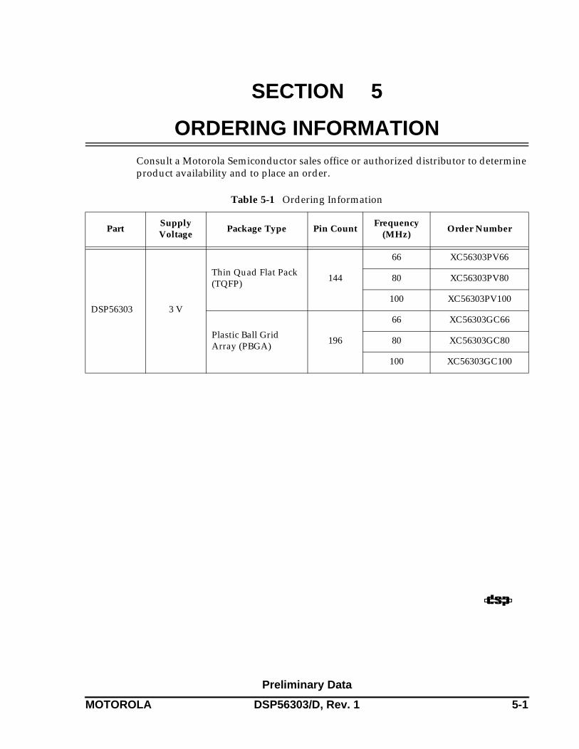
Preliminary Data
MOTOROLA DSP56303/D, Rev. 1 5-1
SECTION 5
ORDERING INFORMATIONConsult a Motorola Semiconductor sales office or authorized distributor to determine product availability and to place an order.
Table 5-1 Ordering Information
PartSupply Voltage
Package Type Pin CountFrequency
(MHz)Order Number
DSP56303 3 V
Thin Quad Flat Pack (TQFP) 144
66 XC56303PV66
80 XC56303PV80
100 XC56303PV100
Plastic Ball Grid Array (PBGA) 196
66 XC56303GC66
80 XC56303GC80
100 XC56303GC100

Preliminary Data
5-2 DSP56303/D, Rev. 1 MOTOROLA
Ordering Information

Preliminary Data
MOTOROLA DSP56303/D, Rev. 1 A-1
APPENDIX A
POWER CONSUMPTION BENCHMARKThe following benchmark program permits evaluation of DSP power usage in a test situation. It enables the PLL, disables the external clock, and uses repeated multiply-accumulate (MAC) instructions with a set of synthetic DSP application data to emulate intensive sustained DSP operation.
;**************************************************************************;**************************************************************************;* *;* CHECKS Typical Power Consumption *;* *;**************************************************************************
page 200,55,0,0,0nolist
I_VEC EQU $000000 ; Interrupt vectors for program debug onlySTART EQU $8000 ; MAIN (external) program starting addressINT_PROG EQU $100 ; INTERNAL program memory starting addressINT_XDAT EQU $0 ; INTERNAL X-data memory starting address INT_YDAT EQU $0 ; INTERNAL Y-data memory starting address
INCLUDE "ioequ.asm"INCLUDE "intequ.asm"
list
org P:START;
movep #$0123FF,x:M_BCR; BCR: Area 3 : 1 w.s (SRAM); Default: 1 w.s (SRAM);
movep #$0d0000,x:M_PCTL ; XTAL disable; PLL enable; CLKOUT disable
;; Load the program;
move #INT_PROG,r0move #PROG_START,r1do #(PROG_END-PROG_START),PLOAD_LOOPmove p:(r1)+,x0move x0,p:(r0)+nop

Preliminary Data
A-2 DSP56303/D, Rev. 1 MOTOROLA
Power Consumption Benchmark
PLOAD_LOOP;; Load the X-data;
move #INT_XDAT,r0move #XDAT_START,r1do #(XDAT_END-XDAT_START),XLOAD_LOOPmove p:(r1)+,x0move x0,x:(r0)+
XLOAD_LOOP;; Load the Y-data;
move #INT_YDAT,r0move #YDAT_START,r1do #(YDAT_END-YDAT_START),YLOAD_LOOPmove p:(r1)+,x0move x0,y:(r0)+
YLOAD_LOOP;
jmp INT_PROG
PROG_STARTmove #$0,r0move #$0,r4move #$3f,m0move #$3f,m4
;clr aclr bmove #$0,x0move #$0,x1move #$0,y0move #$0,y1bset #4,omr ; ebd
;sbr dor #60,_end
mac x0,y0,a x:(r0)+,x1 y:(r4)+,y1mac x1,y1,a x:(r0)+,x0 y:(r4)+,y0add a,bmac x0,y0,a x:(r0)+,x1mac x1,y1,a y:(r4)+,y0move b1,x:$ff
_endbra sbrnop nopnopnop
PROG_ENDnopnop

Power Consumption Benchmark
Preliminary Data
MOTOROLA DSP56303/D, Rev. 1 A-3
XDAT_START; org x:0
dc $262EB9dc $86F2FEdc $E56A5Fdc $616CACdc $8FFD75dc $9210Adc $A06D7Bdc $CEA798dc $8DFBF1dc $A063D6dc $6C6657dc $C2A544dc $A3662Ddc $A4E762dc $84F0F3dc $E6F1B0dc $B3829dc $8BF7AEdc $63A94Fdc $EF78DCdc $242DE5dc $A3E0BAdc $EBAB6Bdc $8726C8dc $CA361dc $2F6E86dc $A57347dc $4BE774dc $8F349Ddc $A1ED12dc $4BFCE3dc $EA26E0dc $CD7D99dc $4BA85Edc $27A43Fdc $A8B10Cdc $D3A55dc $25EC6Adc $2A255Bdc $A5F1F8dc $2426D1dc $AE6536dc $CBBC37dc $6235A4dc $37F0Ddc $63BEC2dc $A5E4D3dc $8CE810dc $3FF09

Preliminary Data
A-4 DSP56303/D, Rev. 1 MOTOROLA
Power Consumption Benchmark
dc $60E50Edc $CFFB2Fdc $40753Cdc $8262C5dc $CA641Adc $EB3B4Bdc $2DA928dc $AB6641dc $28A7E6dc $4E2127dc $482FD4dc $7257Ddc $E53C72dc $1A8C3dc $E27540
XDAT_END
YDAT_START; org y:0
dc $5B6DAdc $C3F70Bdc $6A39E8dc $81E801dc $C666A6dc $46F8E7dc $AAEC94dc $24233Ddc $802732dc $2E3C83dc $A43E00dc $C2B639dc $85A47Edc $ABFDDFdc $F3A2Cdc $2D7CF5dc $E16A8Adc $ECB8FBdc $4BED18dc $43F371dc $83A556dc $E1E9D7dc $ACA2C4dc $8135ADdc $2CE0E2dc $8F2C73dc $432730dc $A87FA9dc $4A292Edc $A63CCFdc $6BA65Cdc $E06D65dc $1AA3Adc $A1B6EB

Power Consumption Benchmark
Preliminary Data
MOTOROLA DSP56303/D, Rev. 1 A-5
dc $48AC48dc $EF7AE1dc $6E3006dc $62F6C7dc $6064F4dc $87E41Ddc $CB2692dc $2C3863dc $C6BC60dc $43A519dc $6139DEdc $ADF7BFdc $4B3E8Cdc $6079D5dc $E0F5EAdc $8230DBdc $A3B778dc $2BFE51dc $E0A6B6dc $68FFB7dc $28F324dc $8F2E8Ddc $667842dc $83E053dc $A1FD90dc $6B2689dc $85B68Edc $622EAFdc $6162BCdc $E4A245
YDAT_END
;**************************************************************************;; EQUATES for DSP56303 I/O registers and ports;; Last update: June 11 1995;;**************************************************************************
page 132,55,0,0,0opt mex
ioequ ident 1,0
;------------------------------------------------------------------------;; EQUATES for I/O Port Programming;

Preliminary Data
A-6 DSP56303/D, Rev. 1 MOTOROLA
Power Consumption Benchmark
;------------------------------------------------------------------------
; Register Addresses
M_HDR EQU $FFFFC9 ; Host port GPIO data RegisterM_HDDR EQU $FFFFC8 ; Host port GPIO direction RegisterM_PCRC EQU $FFFFBF ; Port C Control RegisterM_PRRC EQU $FFFFBE ; Port C Direction RegisterM_PDRC EQU $FFFFBD ; Port C GPIO Data RegisterM_PCRD EQU $FFFFAF ; Port D Control registerM_PRRD EQU $FFFFAE ; Port D Direction Data RegisterM_PDRD EQU $FFFFAD ; Port D GPIO Data RegisterM_PCRE EQU $FFFF9F ; Port E Control registerM_PRRE EQU $FFFF9E ; Port E Direction RegisterM_PDRE EQU $FFFF9D ; Port E Data RegisterM_OGDB EQU $FFFFFC ; OnCE GDB Register
;------------------------------------------------------------------------;; EQUATES for Host Interface;;------------------------------------------------------------------------
; Register Addresses M_HCR EQU $FFFFC2 ; Host Control RegisterM_HSR EQU $FFFFC3 ; Host Status RgisterM_HPCR EQU $FFFFC4 ; Host Polarity Control RegisterM_HBAR EQU $FFFFC5 ; Host Base Address RegisterM_HRX EQU $FFFFC6 ; Host Receive RegisterM_HTX EQU $FFFFC7 ; Host Transmit Register
; HCR bits definitionM_HRIE EQU $0 ; Host Receive interrupts EnableM_HTIE EQU $1 ; Host Transmit Interrupt EnableM_HCIE EQU $2 ; Host Command Interrupt EnableM_HF2 EQU $3 ; Host Flag 2M_HF3 EQU $4 ; Host Flag 3
; HSR bits definitionM_HRDF EQU $0 ; Host Receive Data FullM_HTDE EQU $1 ; Host Receive Data EmptiyM_HCP EQU $2 ; Host Command PendingM_HF0 EQU $3 ; Host Flag 0M_HF1 EQU $4 ; Host Flag 1
; HPCR bits definitionM_HGEN EQU $0 ; Host Port GPIO Enable

Power Consumption Benchmark
Preliminary Data
MOTOROLA DSP56303/D, Rev. 1 A-7
M_HA8EN EQU $1 ; Host Address 8 EnableM_HA9EN EQU $2 ; Host Address 9 EnableM_HCSEN EQU $3 ; Host Chip Select EnableM_HREN EQU $4 ; Host Request EnableM_HAEN EQU $5 ; Host Acknowledge EnableM_HEN EQU $6 ; Host EnableM_HOD EQU $8 ; Host Request Open Drain modeM_HDSP EQU $9 ; Host Data Strobe PolarityM_HASP EQU $A ; Host Address Strobe PolarityM_HMUX EQU $B ; Host Multiplexed bus selectM_HD_HS EQU $C ; Host Double/Single Strobe selectM_HCSP EQU $D ; Host Chip Select PolarityM_HRP EQU $E ; Host Request PolarityPolarityM_HAP EQU $F ; Host Acknowledge Polarity
;------------------------------------------------------------------------;; EQUATES for Serial Communications Interface (SCI);;------------------------------------------------------------------------
; Register Addresses
M_STXH EQU $FFFF97 ; SCI Transmit Data Register (high)M_STXM EQU $FFFF96 ; SCI Transmit Data Register (middle)M_STXL EQU $FFFF95 ; SCI Transmit Data Register (low)M_SRXH EQU $FFFF9A ; SCI Receive Data Register (high)M_SRXM EQU $FFFF99 ; SCI Receive Data Register (middle)M_SRXL EQU $FFFF98 ; SCI Receive Data Register (low)M_STXA EQU $FFFF94 ; SCI Transmit Address RegisterM_SCR EQU $FFFF9C ; SCI Control RegisterM_SSR EQU $FFFF93 ; SCI Status RegisterM_SCCR EQU $FFFF9B ; SCI Clock Control Register
; SCI Control Register Bit Flags
M_WDS EQU $7 ; Word Select Mask (WDS0-WDS3)M_WDS0 EQU 0 ; Word Select 0M_WDS1 EQU 1 ; Word Select 1M_WDS2 EQU 2 ; Word Select 2M_SSFTD EQU 3 ; SCI Shift Direction M_SBK EQU 4 ; Send BreakM_WAKE EQU 5 ; Wakeup Mode SelectM_RWU EQU 6 ; Receiver Wakeup EnableM_WOMS EQU 7 ; Wired-OR Mode SelectM_SCRE EQU 8 ; SCI Receiver EnableM_SCTE EQU 9 ; SCI Transmitter EnableM_ILIE EQU 10 ; Idle Line Interrupt EnableM_SCRIE EQU 11 ; SCI Receive Interrupt EnableM_SCTIE EQU 12 ; SCI Transmit Interrupt Enable

Preliminary Data
A-8 DSP56303/D, Rev. 1 MOTOROLA
Power Consumption Benchmark
M_TMIE EQU 13 ; Timer Interrupt EnableM_TIR EQU 14 ; Timer Interrupt RateM_SCKP EQU 15 ; SCI Clock PolarityM_REIE EQU 16 ; SCI Error Interrupt Enable (REIE)
; SCI Status Register Bit Flags
M_TRNE EQU 0 ; Transmitter EmptyM_TDRE EQU 1 ; Transmit Data Register EmptyM_RDRF EQU 2 ; Receive Data Register FullM_IDLE EQU 3 ; Idle Line FlagM_OR EQU 4 ; Overrun Error Flag M_PE EQU 5 ; Parity ErrorM_FE EQU 6 ; Framing Error FlagM_R8 EQU 7 ; Received Bit 8 (R8) Address
; SCI Clock Control Register
M_CD EQU $FFF ; Clock Divider Mask (CD0-CD11)M_COD EQU 12 ; Clock Out DividerM_SCP EQU 13 ; Clock PrescalerM_RCM EQU 14 ; Receive Clock Mode Source BitM_TCM EQU 15 ; Transmit Clock Source Bit
;------------------------------------------------------------------------;; EQUATES for Synchronous Serial Interface (SSI);;------------------------------------------------------------------------
;; Register Addresses Of SSI0 M_TX00 EQU $FFFFBC ; SSI0 Transmit Data Register 0M_TX01 EQU $FFFFBB ; SSIO Transmit Data Register 1M_TX02 EQU $FFFFBA ; SSIO Transmit Data Register 2M_TSR0 EQU $FFFFB9 ; SSI0 Time Slot RegisterM_RX0 EQU $FFFFB8 ; SSI0 Receive Data RegisterM_SSISR0 EQU $FFFFB7 ; SSI0 Status RegisterM_CRB0 EQU $FFFFB6 ; SSI0 Control Register BM_CRA0 EQU $FFFFB5 ; SSI0 Control Register AM_TSMA0 EQU $FFFFB4 ; SSI0 Transmit Slot Mask Register AM_TSMB0 EQU $FFFFB3 ; SSI0 Transmit Slot Mask Register BM_RSMA0 EQU $FFFFB2 ; SSI0 Receive Slot Mask Register AM_RSMB0 EQU $FFFFB1 ; SSI0 Receive Slot Mask Register B
; Register Addresses Of SSI1 M_TX10 EQU $FFFFAC ; SSI1 Transmit Data Register 0M_TX11 EQU $FFFFAB ; SSI1 Transmit Data Register 1M_TX12 EQU $FFFFAA ; SSI1 Transmit Data Register 2M_TSR1 EQU $FFFFA9 ; SSI1 Time Slot Register

Power Consumption Benchmark
Preliminary Data
MOTOROLA DSP56303/D, Rev. 1 A-9
M_RX1 EQU $FFFFA8 ; SSI1 Receive Data RegisterM_SSISR1 EQU $FFFFA7 ; SSI1 Status RegisterM_CRB1 EQU $FFFFA6 ; SSI1 Control Register BM_CRA1 EQU $FFFFA5 ; SSI1 Control Register AM_TSMA1 EQU $FFFFA4 ; SSI1 Transmit Slot Mask Register AM_TSMB1 EQU $FFFFA3 ; SSI1 Transmit Slot Mask Register BM_RSMA1 EQU $FFFFA2 ; SSI1 Receive Slot Mask Register AM_RSMB1 EQU $FFFFA1 ; SSI1 Receive Slot Mask Register B
; SSI Control Register A Bit Flags
M_PM EQU $FF ; Prescale Modulus Select Mask (PM0-PM7) M_PSR EQU 11 ; Prescaler Range M_DC EQU $1F000 ; Frame Rate Divider Control Mask (DC0-DC7)M_ALC EQU 18 ; Alignment Control (ALC)M_WL EQU $380000 ; Word Length Control Mask (WL0-WL7)M_SSC1 EQU 22 ; Select SC1 as TR #0 drive enable (SSC1)
; SSI Control Register B Bit Flags
M_OF EQU $3 ; Serial Output Flag MaskM_OF0 EQU 0 ; Serial Output Flag 0 M_OF1 EQU 1 ; Serial Output Flag 1 M_SCD EQU $1C ; Serial Control Direction Mask M_SCD0 EQU 2 ; Serial Control 0 Direction M_SCD1 EQU 3 ; Serial Control 1 Direction M_SCD2 EQU 4 ; Serial Control 2 Direction M_SCKD EQU 5 ; Clock Source DirectionM_SHFD EQU 6 ; Shift Direction M_FSL EQU $180 ; Frame Sync Length Mask (FSL0-FSL1)M_FSL0 EQU 7 ; Frame Sync Length 0M_FSL1 EQU 8 ; Frame Sync Length 1M_FSR EQU 9 ; Frame Sync Relative TimingM_FSP EQU 10 ; Frame Sync PolarityM_CKP EQU 11 ; Clock Polarity M_SYN EQU 12 ; Sync/Async Control M_MOD EQU 13 ; SSI Mode SelectM_SSTE EQU $1C000 ; SSI Transmit enable Mask M_SSTE2 EQU 14 ; SSI Transmit #2 Enable M_SSTE1 EQU 15 ; SSI Transmit #1 Enable M_SSTE0 EQU 16 ; SSI Transmit #0 Enable M_SSRE EQU 17 ; SSI Receive Enable M_SSTIE EQU 18 ; SSI Transmit Interrupt Enable M_SSRIE EQU 19 ; SSI Receive Interrupt Enable M_STLIE EQU 20 ; SSI Transmit Last Slot Interrupt Enable M_SRLIE EQU 21 ; SSI Receive Last Slot Interrupt Enable M_STEIE EQU 22 ; SSI Transmit Error Interrupt Enable M_SREIE EQU 23 ; SI Receive Error Interrupt Enable
; SSI Status Register Bit Flags
M_IF EQU $3 ; Serial Input Flag Mask M_IF0 EQU 0 ; Serial Input Flag 0

Preliminary Data
A-10 DSP56303/D, Rev. 1 MOTOROLA
Power Consumption Benchmark
M_IF1 EQU 1 ; Serial Input Flag 1 M_TFS EQU 2 ; Transmit Frame Sync Flag M_RFS EQU 3 ; Receive Frame Sync Flag M_TUE EQU 4 ; Transmitter Underrun Error FLag M_ROE EQU 5 ; Receiver Overrun Error Flag M_TDE EQU 6 ; Transmit Data Register Empty M_RDF EQU 7 ; Receive Data Register Full
; SSI Transmit Slot Mask Register A
M_SSTSA EQU $FFFF ; SSI Transmit Slot Bits Mask A (TS0-TS15)
; SSI Transmit Slot Mask Register B
M_SSTSB EQU $FFFF ; SSI Transmit Slot Bits Mask B (TS16-TS31)
; SSI Receive Slot Mask Register A
M_SSRSA EQU $FFFF ; SSI Receive Slot Bits Mask A (RS0-RS15) ; SSI Receive Slot Mask Register B
M_SSRSB EQU $FFFF ; SSI Receive Slot Bits Mask B (RS16-RS31)
;------------------------------------------------------------------------;; EQUATES for Exception Processing ;;------------------------------------------------------------------------
; Register Addresses
M_IPRC EQU $FFFFFF ; Interrupt Priority Register CoreM_IPRP EQU $FFFFFE ; Interrupt Priority Register Peripheral
; Interrupt Priority Register Core (IPRC)
M_IAL EQU $7 ; IRQA Mode MaskM_IAL0 EQU 0 ; IRQA Mode Interrupt Priority Level (low)M_IAL1 EQU 1 ; IRQA Mode Interrupt Priority Level (high)M_IAL2 EQU 2 ; IRQA Mode Trigger ModeM_IBL EQU $38 ; IRQB Mode MaskM_IBL0 EQU 3 ; IRQB Mode Interrupt Priority Level (low)M_IBL1 EQU 4 ; IRQB Mode Interrupt Priority Level (high)M_IBL2 EQU 5 ; IRQB Mode Trigger ModeM_ICL EQU $1C0 ; IRQC Mode MaskM_ICL0 EQU 6 ; IRQC Mode Interrupt Priority Level (low)M_ICL1 EQU 7 ; IRQC Mode Interrupt Priority Level (high)

Power Consumption Benchmark
Preliminary Data
MOTOROLA DSP56303/D, Rev. 1 A-11
M_ICL2 EQU 8 ; IRQC Mode Trigger ModeM_IDL EQU $E00 ; IRQD Mode MaskM_IDL0 EQU 9 ; IRQD Mode Interrupt Priority Level (low)M_IDL1 EQU 10 ; IRQD Mode Interrupt Priority Level (high)M_IDL2 EQU 11 ; IRQD Mode Trigger ModeM_D0L EQU $3000 ; DMA0 Interrupt priority Level MaskM_D0L0 EQU 12 ; DMA0 Interrupt Priority Level (low)M_D0L1 EQU 13 ; DMA0 Interrupt Priority Level (high)M_D1L EQU $C000 ; DMA1 Interrupt Priority Level MaskM_D1L0 EQU 14 ; DMA1 Interrupt Priority Level (low)M_D1L1 EQU 15 ; DMA1 Interrupt Priority Level (high)M_D2L EQU $30000 ; DMA2 Interrupt priority Level MaskM_D2L0 EQU 16 ; DMA2 Interrupt Priority Level (low)M_D2L1 EQU 17 ; DMA2 Interrupt Priority Level (high)M_D3L EQU $C0000 ; DMA3 Interrupt Priority Level MaskM_D3L0 EQU 18 ; DMA3 Interrupt Priority Level (low)M_D3L1 EQU 19 ; DMA3 Interrupt Priority Level (high)M_D4L EQU $300000 ; DMA4 Interrupt priority Level MaskM_D4L0 EQU 20 ; DMA4 Interrupt Priority Level (low)M_D4L1 EQU 21 ; DMA4 Interrupt Priority Level (high)M_D5L EQU $C00000 ; DMA5 Interrupt priority Level MaskM_D5L0 EQU 22 ; DMA5 Interrupt Priority Level (low)M_D5L1 EQU 23 ; DMA5 Interrupt Priority Level (high)
; Interrupt Priority Register Peripheral (IPRP)
M_HPL EQU $3 ; Host Interrupt Priority Level MaskM_HPL0 EQU 0 ; Host Interrupt Priority Level (low)M_HPL1 EQU 1 ; Host Interrupt Priority Level (high)M_S0L EQU $C ; SSI0 Interrupt Priority Level MaskM_S0L0 EQU 2 ; SSI0 Interrupt Priority Level (low)M_S0L1 EQU 3 ; SSI0 Interrupt Priority Level (high)M_S1L EQU $30 ; SSI1 Interrupt Priority Level MaskM_S1L0 EQU 4 ; SSI1 Interrupt Priority Level (low)M_S1L1 EQU 5 ; SSI1 Interrupt Priority Level (high)M_SCL EQU $C0 ; SCI Interrupt Priority Level Mask M_SCL0 EQU 6 ; SCI Interrupt Priority Level (low)M_SCL1 EQU 7 ; SCI Interrupt Priority Level (high)M_T0L EQU $300 ; TIMER Interrupt Priority Level MaskM_T0L0 EQU 8 ; TIMER Interrupt Priority Level (low)M_T0L1 EQU 9 ; TIMER Interrupt Priority Level (high)
;------------------------------------------------------------------------;; EQUATES for TIMER ;;------------------------------------------------------------------------
; Register Addresses Of TIMER0

Preliminary Data
A-12 DSP56303/D, Rev. 1 MOTOROLA
Power Consumption Benchmark
M_TCSR0 EQU $FFFF8F ; Timer 0 Control/Status Register M_TLR0 EQU $FFFF8E ; TIMER0 Load Reg M_TCPR0 EQU $FFFF8D ; TIMER0 Compare RegisterM_TCR0 EQU $FFFF8C ; TIMER0 Count Register
; Register Addresses Of TIMER1
M_TCSR1 EQU $FFFF8B ; TIMER1 Control/Status Register M_TLR1 EQU $FFFF8A ; TIMER1 Load Reg M_TCPR1 EQU $FFFF89 ; TIMER1 Compare RegisterM_TCR1 EQU $FFFF88 ; TIMER1 Count Register
; Register Addresses Of TIMER2
M_TCSR2 EQU $FFFF87 ; TIMER2 Control/Status Register M_TLR2 EQU $FFFF86 ; TIMER2 Load Reg M_TCPR2 EQU $FFFF85 ; TIMER2 Compare RegisterM_TCR2 EQU $FFFF84 ; TIMER2 Count RegisterM_TPLR EQU $FFFF83 ; TIMER Prescaler Load RegisterM_TPCR EQU $FFFF82 ; TIMER Prescalar Count Register
; Timer Control/Status Register Bit Flags
M_TE EQU 0 ; Timer Enable M_TOIE EQU 1 ; Timer Overflow Interrupt EnableM_TCIE EQU 2 ; Timer Compare Interrupt EnableM_TC EQU $F0 ; Timer Control Mask (TC0-TC3)M_INV EQU 8 ; Inverter BitM_TRM EQU 9 ; Timer Restart Mode M_DIR EQU 11 ; Direction BitM_DI EQU 12 ; Data InputM_DO EQU 13 ; Data OutputM_PCE EQU 15 ; Prescaled Clock EnableM_TOF EQU 20 ; Timer Overflow FlagM_TCF EQU 21 ; Timer Compare Flag
; Timer Prescaler Register Bit Flags
M_PS EQU $600000 ; Prescaler Source MaskM_PS0 EQU 21M_PS1 EQU 22
; Timer Control BitsM_TC0 EQU 4 ; Timer Control 0M_TC1 EQU 5 ; Timer Control 1M_TC2 EQU 6 ; Timer Control 2M_TC3 EQU 7 ; Timer Control 3
Power Consumption Benchmark
Preliminary Data
MOTOROLA DSP56303/D, Rev. 1 A-13
;------------------------------------------------------------------------;; EQUATES for Direct Memory Access (DMA) ;;------------------------------------------------------------------------
; Register Addresses Of DMAM_DSTR EQU FFFFF4 ; DMA Status RegisterM_DOR0 EQU $FFFFF3 ; DMA Offset Register 0M_DOR1 EQU $FFFFF2 ; DMA Offset Register 1M_DOR2 EQU $FFFFF1 ; DMA Offset Register 2M_DOR3 EQU $FFFFF0 ; DMA Offset Register 3
; Register Addresses Of DMA0
M_DSR0 EQU $FFFFEF ; DMA0 Source Address RegisterM_DDR0 EQU $FFFFEE ; DMA0 Destination Address Register M_DCO0 EQU $FFFFED ; DMA0 CounterM_DCR0 EQU $FFFFEC ; DMA0 Control Register
; Register Addresses Of DMA1
M_DSR1 EQU $FFFFEB ; DMA1 Source Address RegisterM_DDR1 EQU $FFFFEA ; DMA1 Destination Address Register M_DCO1 EQU $FFFFE9 ; DMA1 CounterM_DCR1 EQU $FFFFE8 ; DMA1 Control Register
; Register Addresses Of DMA2
M_DSR2 EQU $FFFFE7 ; DMA2 Source Address RegisterM_DDR2 EQU $FFFFE6 ; DMA2 Destination Address Register M_DCO2 EQU $FFFFE5 ; DMA2 CounterM_DCR2 EQU $FFFFE4 ; DMA2 Control Register ; Register Addresses Of DMA4
M_DSR3 EQU $FFFFE3 ; DMA3 Source Address RegisterM_DDR3 EQU $FFFFE2 ; DMA3 Destination Address Register M_DCO3 EQU $FFFFE1 ; DMA3 CounterM_DCR3 EQU $FFFFE0 ; DMA3 Control Register
; Register Addresses Of DMA4
M_DSR4 EQU $FFFFDF ; DMA4 Source Address RegisterM_DDR4 EQU $FFFFDE ; DMA4 Destination Address Register M_DCO4 EQU $FFFFDD ; DMA4 CounterM_DCR4 EQU $FFFFDC ; DMA4 Control Register
; Register Addresses Of DMA5

Preliminary Data
A-14 DSP56303/D, Rev. 1 MOTOROLA
Power Consumption Benchmark
M_DSR5 EQU $FFFFDB ; DMA5 Source Address RegisterM_DDR5 EQU $FFFFDA ; DMA5 Destination Address Register M_DCO5 EQU $FFFFD9 ; DMA5 CounterM_DCR5 EQU $FFFFD8 ; DMA5 Control Register
; DMA Control Register
M_DSS EQU $3 ; DMA Source Space Mask (DSS0-Dss1)M_DSS0 EQU 0 ; DMA Source Memory space 0M_DSS1 EQU 1 ; DMA Source Memory space 1M_DDS EQU $C ; DMA Destination Space Mask (DDS-DDS1)M_DDS0 EQU 2 ; DMA Destination Memory Space 0M_DDS1 EQU 3 ; DMA Destination Memory Space 1M_DAM EQU $3f0 ; DMA Address Mode Mask (DAM5-DAM0)M_DAM0 EQU 4 ; DMA Address Mode 0M_DAM1 EQU 5 ; DMA Address Mode 1M_DAM2 EQU 6 ; DMA Address Mode 2M_DAM3 EQU 7 ; DMA Address Mode 3M_DAM4 EQU 8 ; DMA Address Mode 4M_DAM5 EQU 9 ; DMA Address Mode 5M_D3D EQU 10 ; DMA Three Dimensional ModeM_DRS EQU $F800 ; DMA Request Source Mask (DRS0-DRS4)M_DCON EQU 16 ; DMA Continuous ModeM_DPR EQU $60000 ; DMA Channel PriorityM_DPR0 EQU 17 ; DMA Channel Priority Level (low)M_DPR1 EQU 18 ; DMA Channel Priority Level (high)M_DTM EQU $380000 ; DMA Transfer Mode Mask (DTM2-DTM0)M_DTM0 EQU 19 ; DMA Transfer Mode 0M_DTM1 EQU 20 ; DMA Transfer Mode 1M_DTM2 EQU 21 ; DMA Transfer Mode 2M_DIE EQU 22 ; DMA Interrupt Enable bitM_DE EQU 23 ; DMA Channel Enable bit
; DMA Status Register
M_DTD EQU $3F ; Channel Transfer Done Status MASK (DTD0-DTD5)M_DTD0 EQU 0 ; DMA Channel Transfer Done Status 0M_DTD1 EQU 1 ; DMA Channel Transfer Done Status 1M_DTD2 EQU 2 ; DMA Channel Transfer Done Status 2M_DTD3 EQU 3 ; DMA Channel Transfer Done Status 3M_DTD4 EQU 4 ; DMA Channel Transfer Done Status 4M_DTD5 EQU 5 ; DMA Channel Transfer Done Status 5M_DACT EQU 8 ; DMA Active StateM_DCH EQU $E00 ; DMA Active Channel Mask (DCH0-DCH2)M_DCH0 EQU 9 ; DMA Active Channel 0M_DCH1 EQU 10 ; DMA Active Channel 1M_DCH2 EQU 11 ; DMA Active Channel 2
;------------------------------------------------------------------------;

Power Consumption Benchmark
Preliminary Data
MOTOROLA DSP56303/D, Rev. 1 A-15
; EQUATES for Phase Locked Loop (PLL) ;;------------------------------------------------------------------------
; Register Addresses Of PLL
M_PCTL EQU $FFFFFD ; PLL Control Register
; PLL Control Register
M_MF EQU $FFF : Multiplication Factor Bits Mask (MF0-MF11)M_DF EQU $7000 ; Division Factor Bits Mask (DF0-DF2)M_XTLR EQU 15 ; XTAL Range select bitM_XTLD EQU 16 ; XTAL Disable BitM_PSTP EQU 17 ; STOP Processing State Bit M_PEN EQU 18 ; PLL Enable BitM_PCOD EQU 19 ; PLL Clock Output Disable BitM_PD EQU $F00000 ; PreDivider Factor Bits Mask (PD0-PD3)
;------------------------------------------------------------------------;; EQUATES for BIU ;;------------------------------------------------------------------------
; Register Addresses Of BIU
M_BCR EQU $FFFFFB ; Bus Control RegisterM_DCR EQU $FFFFFA ; DRAM Control RegisterM_AAR0 EQU $FFFFF9 ; Address Attribute Register 0 M_AAR1 EQU $FFFFF8 ; Address Attribute Register 1 M_AAR2 EQU $FFFFF7 ; Address Attribute Register 2 M_AAR3 EQU $FFFFF6 ; Address Attribute Register 3 M_IDR EQU $FFFFF5 ; ID Register
; Bus Control Register
M_BA0W EQU $1F ; Area 0 Wait Control Mask (BA0W0-BA0W4)M_BA1W EQU $3E0 ; Area 1 Wait Control Mask (BA1W0-BA14)M_BA2W EQU $1C00 ; Area 2 Wait Control Mask (BA2W0-BA2W2)M_BA3W EQU $E000 ; Area 3 Wait Control Mask (BA3W0-BA3W3)M_BDFW EQU $1F0000 ; Default Area Wait Control Mask (BDFW0-BDFW4)M_BBS EQU 21 ; Bus StateM_BLH EQU 22 ; Bus Lock HoldM_BRH EQU 23 ; Bus Request Hold
; DRAM Control Register
Preliminary Data
A-16 DSP56303/D, Rev. 1 MOTOROLA
Power Consumption Benchmark
M_BCW EQU $3 ; In Page Wait States Bits Mask (BCW0-BCW1)M_BRW EQU $C ; Out Of Page Wait States Bits Mask (BRW0-BRW1)M_BPS EQU $300 ; DRAM Page Size Bits Mask (BPS0-BPS1)M_BPLE EQU 11 ; Page Logic EnableM_BME EQU 12 ; Mastership EnableM_BRE EQU 13 ; Refresh EnableM_BSTR EQU 14 ; Software Triggered RefreshM_BRF EQU $7F8000 ; Refresh Rate Bits Mask (BRF0-BRF7)M_BRP EQU 23 ; Refresh prescaler
; Address Attribute Registers
M_BAT EQU $3 ; Ext. Access Type and Pin Def. Bits Mask (BAT0-BAT1)M_BAAP EQU 2 ; Address Attribute Pin PolarityM_BPEN EQU 3 ; Program Space EnableM_BXEN EQU 4 ; X Data Space EnableM_BYEN EQU 5 ; Y Data Space EnableM_BAM EQU 6 ; Address MuxingM_BPAC EQU 7 ; Packing EnableM_BNC EQU $F00 ; Number of Address Bits to Compare Mask (BNC0-BNC3)M_BAC EQU $FFF000 ; Address to Compare Bits Mask (BAC0-BAC11)
; control and status bits in SR
M_CP EQU $c00000 ; mask for CORE-DMA priority bits in SRM_CA EQU 0 ; CarryM_V EQU 1 ; Overflow M_Z EQU 2 ; ZeroM_N EQU 3 ; Negative M_U EQU 4 ; UnnormalizedM_E EQU 5 ; Extension M_L EQU 6 ; LimitM_S EQU 7 ; Scaling Bit M_I0 EQU 8 ; Interupt Mask Bit 0M_I1 EQU 9 ; Interupt Mask Bit 1M_S0 EQU 10 ; Scaling Mode Bit 0M_S1 EQU 11 ; Scaling Mode Bit 1M_SC EQU 13 ; Sixteen_Bit CompatibilityM_DM EQU 14 ; Double Precision MultiplyM_LF EQU 15 ; DO-Loop FlagM_FV EQU 16 ; DO-Forever FlagM_SA EQU 17 ; Sixteen-Bit ArithmeticM_CE EQU 19 ; Instruction Cache EnableM_SM EQU 20 ; Arithmetic SaturationM_RM EQU 21 ; Rounding ModeM_CP0 EQU 22 ; bit 0 of priority bits in SRM_CP1 EQU 23 ; bit 1 of priority bits in SR
; control and status bits in OMRM_CDP EQU $300 ; mask for CORE-DMA priority bits in OMRM_MA equ0 ; Operating Mode A

Power Consumption Benchmark
Preliminary Data
MOTOROLA DSP56303/D, Rev. 1 A-17
M_MB equ1 ; Operating Mode BM_MC equ2 ; Operating Mode CM_MD equ3 ; Operating Mode DM_EBD EQU 4 ; External Bus Disable bit in OMRM_SD EQU 6 ; Stop Delay M_MS EQU 7 ; Memory Switch bit in OMRM_CDP0 EQU 8 ; bit 0 of priority bits in OMRM_CDP1 EQU 9 ; bit 1 of priority bits in OMRM_BEN EQU 10 ; Burst Enable M_TAS EQU 11 ; TA Synchronize SelectM_BRT EQU 12 ; Bus Release Timing M_ATE EQU 15 ; Address Tracing Enable bit in OMR.M_XYS EQU 16 ; Stack Extension space select bit in OMR.M_EUN EQU 17 ; Extensed stack UNderflow flag in OMR.M_EOV EQU 18 ; Extended stack OVerflow flag in OMR.M_WRP EQU 19 ; Extended WRaP flag in OMR.M_SEN EQU 20 ; Stack Extension Enable bit in OMR.
;*************************************************************************;; EQUATES for DSP56303 interrupts;; Last update: June 11 1995 ;;*************************************************************************
page 132,55,0,0,0opt mex
intequ ident 1,0
if @DEF(I_VEC);leave user definition as is.else
I_VEC EQU $0endif
;------------------------------------------------------------------------; Non-Maskable interrupts;------------------------------------------------------------------------I_RESET EQU I_VEC+$00 ; Hardware RESET
Preliminary Data
A-18 DSP56303/D, Rev. 1 MOTOROLA
Power Consumption Benchmark
I_STACK EQU I_VEC+$02 ; Stack ErrorI_ILL EQU I_VEC+$04 ; Illegal InstructionI_DBG EQU I_VEC+$06 ; Debug Request I_TRAP EQU I_VEC+$08 ; TrapI_NMI EQU I_VEC+$0A ; Non Maskable Interrupt
;------------------------------------------------------------------------; Interrupt Request Pins;------------------------------------------------------------------------I_IRQA EQU I_VEC+$10 ; IRQAI_IRQB EQU I_VEC+$12 ; IRQBI_IRQC EQU I_VEC+$14 ; IRQCI_IRQD EQU I_VEC+$16 ; IRQD
;------------------------------------------------------------------------; DMA Interrupts;------------------------------------------------------------------------I_DMA0 EQU I_VEC+$18 ; DMA Channel 0I_DMA1 EQU I_VEC+$1A ; DMA Channel 1I_DMA2 EQU I_VEC+$1C ; DMA Channel 2I_DMA3 EQU I_VEC+$1E ; DMA Channel 3I_DMA4 EQU I_VEC+$20 ; DMA Channel 4I_DMA5 EQU I_VEC+$22 ; DMA Channel 5
;------------------------------------------------------------------------; Timer Interrupts;------------------------------------------------------------------------I_TIM0C EQU I_VEC+$24 ; TIMER 0 compareI_TIM0OF EQU I_VEC+$26 ; TIMER 0 overflowI_TIM1C EQU I_VEC+$28 ; TIMER 1 compareI_TIM1OF EQU I_VEC+$2A ; TIMER 1 overflowI_TIM2C EQU I_VEC+$2C ; TIMER 2 compareI_TIM2OF EQU I_VEC+$2E ; TIMER 2 overflow
;------------------------------------------------------------------------; ESSI Interrupts;------------------------------------------------------------------------I_SI0RD EQU I_VEC+$30 ; ESSI0 Receive DataI_SI0RDE EQU I_VEC+$32 ; ESSI0 Receive Data w/ exception StatusI_SI0RLS EQU I_VEC+$34 ; ESSI0 Receive last slotI_SI0TD EQU I_VEC+$36 ; ESSI0 Transmit dataI_SI0TDE EQU I_VEC+$38 ; ESSI0 Transmit Data w/ exception StatusI_SI0TLS EQU I_VEC+$3A ; ESSI0 Transmit last slotI_SI1RD EQU I_VEC+$40 ; ESSI1 Receive DataI_SI1RDE EQU I_VEC+$42 ; ESSI1 Receive Data w/ exception Status

Power Consumption Benchmark
Preliminary Data
MOTOROLA DSP56303/D, Rev. 1 A-19
I_SI1RLS EQU I_VEC+$44 ; ESSI1 Receive last slotI_SI1TD EQU I_VEC+$46 ; ESSI1 Transmit dataI_SI1TDE EQU I_VEC+$48 ; ESSI1 Transmit Data w/ exception StatusI_SI1TLS EQU I_VEC+$4A ; ESSI1 Transmit last slot
;------------------------------------------------------------------------; SCI Interrupts;------------------------------------------------------------------------I_SCIRD EQU I_VEC+$50 ; SCI Receive Data I_SCIRDE EQU I_VEC+$52 ; SCI Receive Data With Exception StatusI_SCITD EQU I_VEC+$54 ; SCI Transmit DataI_SCIIL EQU I_VEC+$56 ; SCI Idle LineI_SCITM EQU I_VEC+$58 ; SCI Timer
;------------------------------------------------------------------------; HOST Interrupts;------------------------------------------------------------------------I_HRDF EQU I_VEC+$60 ; Host Receive Data FullI_HTDE EQU I_VEC+$62 ; Host Transmit Data EmptyI_HC EQU I_VEC+$64 ; Default Host Command
;------------------------------------------------------------------------; INTERRUPT ENDING ADDRESS;------------------------------------------------------------------------I_INTEND EQU I_VEC+$FF ; last address of interrupt vector space

MOTOROLA DSP56303UM/AD, Rev. 1 B-1
APPENDIX B
BOOTSTRAP PROGRAMS
; BOOTSTRAP CODE FOR DSP56303 - (C) Copyright 1995 Motorola Inc.; Revised June, 29 1995.;; Bootstrap through the Host Interface, External EPROM or SCI.;; This is the Bootstrap program contained in the DSP56303 192-word Boot; ROM. This program can load any program RAM segment from an external; EPROM, from the Host Interface or from the SCI serial interface.;;;;;;;;;;;;;;;;;;;;;;;;;;;;;;;;;;;;;;;;;;;;;;;;;;;;;;;;;;;;;;;;;;;;;;;;;;;;;; If MD:MC:MB:MA=1000, then the Boot ROM is bypassed and the DSP56303 will; start fetching instructions beginning with the address $8000 assuming that; an external memory of SRAM type is used. The accesses will be performed ; using 31 wait states with no address attributes selected (default area).;;;;;;;;;;;;;;;;;;;;;;;;;;;;;;;;;;;;;;;;;;;;;;;;;;;;;;;;;;;;;;;;;;;;;;;;;;;;;; If MC:MB:MA=001, then it loads a program RAM segment from consecutive; byte-wide P memory locations, starting at P:$D00000 (bits 7-0). ; The memory is selected by the Address Attribute AA1 and is accessed with; 31 wait states.; The EPROM bootstrap code expects to read 3 bytes; specifying the number of program words, 3 bytes specifying the address; to start loading the program words and then 3 bytes for each program; word to be loaded. The number of words, the starting address and the; program words are read least significant byte first followed by the; mid and then by the most significant byte. ; The program words will be condensed into 24-bit words and stored in ; contiguous PRAM memory locations starting at the specified starting : address.; After reading the program words, program execution starts from the same ; address where loading started.;;;;;;;;;;;;;;;;;;;;;;;;;;;;;;;;;;;;;;;;;;;;;;;;;;;;;;;;;;;;;;;;;;;;;;;;;;;;;; If MC:MB:MA=010, then it loads the program RAM from the SCI interface.; The number of program words to be loaded and the starting address must; be specified. The SCI bootstrap code expects to receive 3 bytes

B-2 DSP56303UM/AD, Rev. 1 MOTOROLA
Bootstrap Programs
; specifying the number of program words, 3 bytes specifying the address; to start loading the program words and then 3 bytes for each program; word to be loaded. The number of words, the starting address and the; program words are received least significant byte first followed by the; mid and then by the most significant byte. After receiving the; program words, program execution starts in the same address where; loading started. The SCI is programmed to work in asynchronous mode; with 8 data bits, 1 stop bit and no parity. The clock source is; external and the clock frequency must be 16x the baud rate.; After each byte is received, it is echoed back through the SCI; transmitter. ;;;;;;;;;;;;;;;;;;;;;;;;;;;;;;;;;;;;;;;;;;;;;;;;;;;;;;;;;;;;;;;;;;;;;;;;;;;;;; If MC:MB:MA=100, then it loads the program RAM from the Host; Interface programmed to operate in the ISA mode.; The HOST ISA bootstrap code expects to read a 24-bit word ; specifying the number of program words, a 24-bit word specifying the address; to start loading the program words and then a 24-bit word for each program; word to be loaded. The program words will be stored in ; contiguous PRAM memory locations starting at the specified starting address.; After reading the program words, program execution starts from the same ; address where loading started.; The Host Interface bootstrap load program may be stopped by; setting the Host Flag 0 (HF0). This will start execution of the loaded; program from the specified starting address.;;;;;;;;;;;;;;;;;;;;;;;;;;;;;;;;;;;;;;;;;;;;;;;;;;;;;;;;;;;;;;;;;;;;;;;;;;;;;; If MC:MB:MA=101, then it loads the program RAM from the Host; Interface programmed to operate in the HC11 non multiplexed mode.;; The HOST HC11 bootstrap code expects to read a 24-bit word ; specifying the number of program words, a 24-bit word specifying the address; to start loading the program words and then a 24-bit word for each program; word to be loaded. The program words will be stored in ; contiguous PRAM memory locations starting at the specified starting address.; After reading the program words, program execution starts from the same ; address where loading started.; The Host Interface bootstrap load program may be stopped by; setting the Host Flag 0 (HF0). This will start execution of the loaded; program from the specified starting address.;;;;;;;;;;;;;;;;;;;;;;;;;;;;;;;;;;;;;;;;;;;;;;;;;;;;;;;;;;;;;;;;;;;;;;;;;;;;;; If MC:MB:MA=110, then it loads the program RAM from the Host; Interface programmed to operate in the 8051 multiplexed bus mode,

Bootstrap Programs
MOTOROLA DSP56303UM/AD, Rev. 1 B-3
; in double-strobe pin configuration.; The HOST 8051 bootstrap code expects accesses that are byte wide.; The HOST 8051 bootstrap code expects to read 3 bytes forming a 24-bit word ; specifying the number of program words, 3 bytes forming a 24-bit word ; specifying the address to start loading the program words and then 3 bytes ; forming 24-bit words for each program word to be loaded. ; The program words will be stored in contiguous PRAM memory locations ; starting at the specified starting address.; After reading the program words, program execution starts from the same ; address where loading started.; The Host Interface bootstrap load program may be stopped by setting the ; Host Flag 0 (HF0). This will start execution of the loaded program from ; the specified starting address.;; The base address of the HI08 in multiplexed mode is 0x80 and is not modified; by the bootstrap code. All the address lines are enabled and should be; connected accordingly.;;;;;;;;;;;;;;;;;;;;;;;;;;;;;;;;;;;;;;;;;;;;;;;;;;;;;;;;;;;;;;;;;;;;;;;;;;;;; If MC:MB:MA=111, then it loads the program RAM from the Host; Interface programmed to operate in the MC68302 bus mode, ; in single-strobe pin configuration.; The HOST MC68302 bootstrap code expects accesses that are byte wide.; The HOST MC68302 bootstrap code expects to read 3 bytes forming a 24-bit word ; specifying the number of program words, 3 bytes forming a 24-bit word ; specifying the address to start loading the program words and then 3 bytes ; forming 24-bit words for each program word to be loaded. ; The program words will be stored in contiguous PRAM memory locations ; starting at the specified starting address.; After reading the program words, program execution starts from the same ; address where loading started.; The Host Interface bootstrap load program may be stopped by setting the ; Host Flag 0 (HF0). This will start execution of the loaded program from ; the specified starting address.;
BOOT equ $D00000 ; this is the location in P memory ; on the external memory bus ; where the external byte-wide ; EPROM would be located AARV equ $D00409 ; AAR1 selects the EPROM as CE~ ; mapped as P from $D00000 to ; $DFFFFF, active low
M_SSR EQU $FFFF93 ; SCI Status RegisterM_STXL EQU $FFFF95 ; SCI Transmit Data Register (low)M_SRXL EQU $FFFF98 ; SCI Receive Data Register (low)

B-4 DSP56303UM/AD, Rev. 1 MOTOROLA
Bootstrap Programs
M_SCCR EQU $FFFF9B ; SCI Clock Control RegisterM_SCR EQU $FFFF9C ; SCI Control RegisterM_PCRE EQU $FFFF9F ; Port E Control registerM_AAR1 EQU $FFFFF8 ; Address Attribute Register 1M_HPCR EQU $FFFFC4 ; Host Polarity Control RegisterM_HSR EQU$FFFFC3; Host Status RegisterM_HRX EQU$FFFFC6; Host Receive RegisterHRDF EQU$0 ; Host Receive Data FullHF0 EQU$3 ; Host Flag 0HEN EQU$6 ; Host Enable
ORG PL:$ff0000,PL:$ff0000 ; bootstrap code starts at $ff0000 START clr a #$0a,X0 ; clear a and load X0 with constant 0a0000 jclr #2,omr,EPRSCILD ; If MC:MB:MA=0xx, go load from EPROM/SCI
jclr #1,omr,OMR1IS0; IF MC:MB:MA=10x, go to look for ISA/HC11 options jclr #0,omr,I8051HOSTLD ; If MC:MB:MA=110, go load from 8051 Host jmp MC68302HOSTLD ; If MC:MB:MA=111, go load from MC68302 HostOMR1IS0 jset #0,omr,HC11HOSTLD ; If MC:MB:MA=101, go load from HC11 Host ; If MC:MB:MA=100, go load from ISA HOST
;=============================================================================; This is the routine which loads a program through the HI08 host port; The program is downloaded from the host MCU with the following scenario:; 1) 3 bytes - Define the program length.; 2) 3 bytes - Define the address to which to start loading the program to.; 3) 3n bytes (while n is any integer number); The program words will be stored in contiguous PRAM memory locations starting; at the specified starting address.; After reading the program words, program execution starts from the same address; where loading started.; The host MCU may terminate the loading process by setting the HF1=0 and HF0=1.; When the downloading is terminated, the program will start execution of the; loaded program from the specified starting address.; The HI08 boot ROM program enables the following busses to download programs; through the HI08 port:;; 1 - ISA- Dual strobes non-multiplexed bus with negative strobe; pulses dual positive request; 2 - HC11- Single strobe non-multiplexed bus with positive strobe; pulse single negative request.; 4 - i8051 - Dual strobes multiplexed bus with negative strobe pulses; dual negative request.; 5 - MC68302 - Single strobe non-multiplexed bus with negative strobe

Bootstrap Programs
MOTOROLA DSP56303UM/AD, Rev. 1 B-5
; pulse single negative request.;=============================================================================
ISAHOSTLDmovep #%0101000000011000,x:M_HPCR
; Configure the following conditions:; HAP = 0 Negative host acknowledge; HRP = 1 Positive host request; HCSP= 0 Negative chip select input; HD/HS= 1 Dual strobes bus (RD and WR strobes); HMUX= 0 Non multiplexed bus; HASP= 0 (address strobe polarity has no
; meaning in non-multiplexed bus); HDSP= 0 Negative data strobes polarity; HROD= 0 Host request is active when enabled; spare = 0 This bit should be set to 0 for; future compatibility; HEN = 0 When the HPCR register is modified; HEN should be cleared; HAEN= 0 Host acknowledge is disabled; HREN= 1 Host requests are enabled; HCSEN = 1 Host chip select input enabled; HA9EN= 0 (address 9 enable bit has no meaning in ; non-multiplexed bus); HA8EN= 0 (address 8 enable bit has no meaning in ; non-multiplexed bus); HGEN= 0 Host GPIO pins are disabled
bra <HI08CONTHC11HOSTLD
movep #%0000001000011000,x:M_HPCR; Configure the following conditions:; HAP = 0 Negative host acknowledge; HRP = 0 Negative host request; HCSP= 0 Negative chip select input; HD/HS= 0 Single strobe bus (R/W~ and DS strobes); HMUX= 0 Non multiplexed bus; HASP= 0 (address strobe polarity has no meaning in ; non-multiplexed bus); HDSP= 1 Negative data strobes polarity; HROD= 0 Host request is active when enabled; spare = 0 This bit should be set to 0 for future ; compatibility; HEN = 0 When the HPCR register is modified HEN should be; cleared; HAEN= 0 Host acknowledge is disabled; HREN= 1 Host requests are enabled; HCSEN = 1 Host chip select input enabled

B-6 DSP56303UM/AD, Rev. 1 MOTOROLA
Bootstrap Programs
; HA9EN= 0 (address 9 enable bit has no meaning in ; non-multiplexed bus); HA8EN= 0 (address 8 enable bit has no meaning in ; non-multiplexed bus); HGEN= 0 Host GPIO pins are disabled
bra <HI08CONTI8051HOSTLD
movep #%0001110000011110,x:M_HPCR; Configure the following conditions:; HAP = 0 Negative host acknowledge; HRP = 0 Negative host request; HCSP= 0 Negative chip select input; HD/HS= 1 Dual strobes bus (RD and WR strobes); HMUX= 1 Multiplexed bus; HASP= 1 Positive address strobe polarity; HDSP= 0 Negative data strobes polarity; HROD= 0 Host request is active when enabled; spare = 0 This bit should be set to 0 for future ; compatibility; HEN = 0 When the HPCR register is modified HEN ; should be cleared; HAEN= 0 Host acknowledge is disabled; HREN= 1 Host requests are enabled; HCSEN = 1 Host chip select input enabled; HA9EN= 1 Enable address 9 input; HA8EN= 1 Enable address 8 input; HGEN= 0 Host GPIO pins are disabled
bra <HI08CONTMC68302HOSTLD
movep #%0000000000111000,x:M_HPCR; Configure the following conditions:; HAP = 0 Negative host acknowledge; HRP = 0 Negative host request; HCSP= 0 Negative chip select input; HD/HS= 0 Single strobe bus (R/W~ and DS strobes); HMUX= 0 Non multiplexed bus; HASP= 0 (address strobe polarity has no meaning in ; non-multiplexed bus); HDSP= 0 Negative data strobes polarity; HROD= 0 Host request is active when enabled; spare = 0 This bit should be set to 0 for future ; compatibility; HEN = 0 When the HPCR register is modified HEN should be; cleared; HAEN= 1 Host acknowledge is enabled; HREN= 1 Host requests are enabled; HCSEN = 1 Host chip select input enabled

Bootstrap Programs
MOTOROLA DSP56303UM/AD, Rev. 1 B-7
; HA9EN= 0 (address 9 enable bit has no meaning in ; non-multiplexed bus); HA8EN= 0 (address 8 enable bit has no meaning in ; non-multiplexed bus); HGEN= 0 Host GPIO pins are disabled
HI08CONTbset #HEN,x:M_HPCR ; Enable the HI08 to operate as host
; interface (set HEN=1)jclr #HRDF,x:M_HSR,* ; wait for the program length to be
; writtenmovep x:M_HRX,a0jclr #HRDF,x:M_HSR,* ; wait for the program starting address
; to be writtenmovep x:M_HRX,r0move r0,r1do a0,HI08LOOP ; set a loop with the downloaded length
; countsHI08LL
jset #HRDF,x:M_HSR,HI08NW ; If new word was loaded then jump ;to read that word
jclr #HF0,x:M_HSR,HI08LL ; If HF0=0 then continue with the; downloading
enddo ; Must terminate the do loopbra <HI08LOOP
HI08NWmovep x:M_HRX,p:(r0)+ ; Move the new word into its destination
; location in the program RAMHI08LOOP
bra <FINISH;========================================================================EPRSCILD jclr #1,omr,EPROMLD ; If MC:MB:MA=001, go load from EPROM
;========================================================================; This is the routine that loads from the SCI.; MC:MB:MA=010 - external SCI clock
SCILD movep #$0302,X:M_SCR ; Configure SCI Control Reg movep #$C000,X:M_SCCR ; Configure SCI Clock Control Reg movep #7,X:M_PCRE ; Configure SCLK, TXD and RXD
do #6,_LOOP6 ; get 3 bytes for number of ; program words and 3 bytes ; for the starting address jclr #2,X:M_SSR,* ; Wait for RDRF to go high movep X:M_SRXL,A2 ; Put 8 bits in A2

B-8 DSP56303UM/AD, Rev. 1 MOTOROLA
Bootstrap Programs
jclr #1,X:M_SSR,* ; Wait for TDRE to go high movep A2,X:M_STXL ; echo the received byte asr #8,a,a_LOOP6 move a1,r0 ; starting address for load move a1,r1 ; save starting address
do a0,_LOOP7 ; Receive program words do #3,_LOOP8 jclr #2,X:M_SSR,* ; Wait for RDRF to go high movep X:M_SRXL,A2 ; Put 8 bits in A2 jclr #1,X:M_SSR,* ; Wait for TDRE to go high movep a2,X:M_STXL ; echo the received byte asr #8,a,a_LOOP8 movem a1,p:(r0)+ ; Store 24-bit result in P mem._LOOP7 bra <FINISH ; Boot from SCI done
;========================================================================; This is the routine that loads from external EPROM.; MC:MB:MA=001 EPROMLD move #BOOT,r2 ; r2 = address of external EPROM movep #AARV,X:M_AAR1 ; aar1 configured for SRAM types of access
do #6,_LOOP9 ; read number of words and starting address movem p:(r2)+,a2 ; Get the 8 LSB from ext. P mem. asr #8,a,a ; Shift 8 bit data into A1_LOOP9 ; move a1,r0 ; starting address for load move a1,r1 ; save it in r1 ; a0 holds the number of words
do a0,_LOOP10 ; read program words do #3,_LOOP11 ; Each instruction has 3 bytes movem p:(r2)+,a2 ; Get the 8 LSB from ext. P mem. asr #8,a,a ; Shift 8 bit data into A1_LOOP11 ; Go get another byte. movem a1,p:(r0)+ ; Store 24-bit result in P mem._LOOP10 ; and go get another 24-bit word. ; Boot from EPROM done;========================================================================FINISH

Bootstrap Programs
MOTOROLA DSP56303UM/AD, Rev. 1 B-9
; This is the exit handler that returns execution to normal; expanded mode and jumps to the RESET vector.
andi #$0,ccr ; Clear CCR as if RESET to 0. jmp (r1) ; Then go to starting Prog addr.
; End of bootstrap code. Number of program words: 91

B-10 DSP56303UM/AD, Rev. 1 MOTOROLA
Bootstrap Programs

Preliminary Data
MOTOROLA DSP56303/D, Rev. 1 Index-1
INDEX
Numerics
5 V tolerance 1-1
A
ac electrical characteristics 2-4address bus 1-1Address Trace mode iii, 2-52, 2-56address, electronic mail iiALU iiiapplications varbitration bus timings 2-56Arithmetic Logic Unit iii
B
benchmark test algorithm A-1bootstrap ROM iiiBoundary Scan (JTAG Port) timing diagram 2-
79bus
address 1-2data 1-2external address 1-6external data 1-6multiplexed 1-2non-multiplexed 1-2
bus acquisition timings 2-57bus control 1-1bus release timings 2-58, 2-59
C
Clock 1-5clock 1-1
external 2-5operation 2-7
clocksinternal 2-5
contents iicrystal oscillator circuits 2-6
D
Data Arithmetic Logic Unit iiidata bus 1-1data memory expansion iv
dc electrical characteristics 2-3Debug support iiidescription, general 1design considerations
electrical 4-3PLL 4-5, 4-6power consumption 4-4thermal 4-1, 4-2
Direct Memory Access iiiDMA iiidocument conventions iidocumentation list viDouble Data Strobe 1-2DRAM
out of pageread access 2-49wait states selection guide 2-37write access 2-50
out of page and refresh timings11 wait states 2-4315 wait states 2-464 wait states 2-378 wait states 2-40
Page moderead accesses 2-36wait states selection guide 2-26write accesses 2-35
Page mode timings1 wait state 2-272 wait states 2-293 wait states 2-314 wait states 2-33
refresh access 2-51DRAM controller ivDS 1-2DSP56300
core features iiiFamily Manual vi
DSP56303block diagram 1description 1features iiispecifications 2-1

Index
Preliminary Data
Index-2 DSP56303/D, Rev. 1 MOTOROLA
Technical Data viUser’s Manual vi
E
electrical design considerations 4-3Enhanced Synchronous Serial Interface 1-1, 1-16,
1-17, 1-18, 1-19, 1-20, 1-21Enhanced Synchronous Serial Interfaces vESSI v, 1-1, 1-2, 1-16, 1-17, 1-18, 1-19, 1-20,
1-21receiver timing 2-74timings 2-70transmitter timing 2-73
external address bus 1-6external bus control 1-6, 1-7, 1-8external bus synchronous timings (SRAM access)
2-52external clock operation 2-5external data bus 1-6external interrupt timing (negative edge-triggered)
2-18external level-sensitive fast interrupt timing 2-18external memory access (DMA Source) timing 2-
20External Memory Expansion Port 1-6, 2-21
F
functional groups 1-2functional signal groups 1-1
G
general description 1General Purpose Input/Output vGPIO v, 1-2, 1-23
Timers 1-2GPIO timing 2-77Ground 1-4
PLL 1-4ground 1-1
H
helpline electronic mail (email) address iiHI08 v, 1-1, 1-2, 1-11, 1-12, 1-13, 1-14, 1-15Host Interface v, 1-1, 1-2, 1-11, 1-12, 1-13, 1-
14, 1-15Host Interface timing 2-60host port
configuration 1-12usage considerations 1-11
Host RequestDouble 1-2Single 1-2
HR 1-2
I
information sources viinstruction cache iiiinternal clocks 2-5internet address iiinterrupt and mode control 1-1, 1-9, 1-10interrupt control 1-9, 1-10interrupt timing 2-10
external level-sensitive fast 2-18external negative edge-triggered 2-18synchronous from Wait state 2-19
J
JTAG 1-24JTAG Port iii
reset timing diagram 2-80timing 2-78, 2-79
JTAG/OnCE port 1-1
M
maximum ratings 2-1, 2-2Memory Expansion Port iiimode control 1-9, 1-10Mode select timing 2-10multiplexed bus 1-2multiplexed bus timings
read 2-65write 2-66
N
non-multiplexed bus 1-2non-multiplexed bus timings
read 2-63write 2-64
O
off-chip memory iiiOnCE
module timing 2-80OnCE module iii, 1-24
Debug request 2-80OnCE/JTAG 1-2on-chip DRAM controller ivOn-Chip Emulation module iii

Preliminary Data
MOTOROLA DSP56303/D, Rev. 1 Index-3
Index
on-chip memory iiioperating mode select timing 2-19ordering information 5-1
P
package144-pin TQFP 3-1196-pin PBGA 3-1PBGA description 3-10, 3-11, 3-12, 3-15, 3-
19TQFP description 3-2, 3-3, 3-4, 3-6, 3-9
PBGA 3-1ball grid drawing (bottom) 3-11ball grid drawing (top) 3-10ball list by name 3-15ball list by number 3-12mechanical drawing 3-19
PCU iiiPhase Lock Loop iii, 2-9PLL iii, 1-1, 1-5, 2-9
Characteristics 2-9performance issues 4-5
PLL design considerations 4-5, 4-6PLL performance issues 4-6Port A 1-1, 1-6Port B 1-1, 1-2, 1-12, 1-13, 1-14, 1-15Port C 1-1, 1-2, 1-16, 1-17, 1-18Port D 1-1, 1-2, 1-19, 1-20, 1-21Port E 1-1, 1-22Power 1-3power 1-1power consumption benchmark test A-1power consumption design considerations 4-4power management vProgram Control Unit iiiprogram memory expansion ivprogram RAM iii
R
recovery from Stop state using IRQA 2-19, 2-20RESET 1-9Reset timing 2-10, 2-17
synchronous 2-17ROM, bootstrap iii
S
SCI v, 1-2, 1-22Asynchronous mode timing 2-69Synchronous mode timing 2-69timing 2-67
Serial Communications Interface v, 1-22Serial Communications Interface (SCI) 1-1signal groupings 1-1signals 1-1
functional grouping 1-2Single Data Strobe 1-2SRAM 2-54
Access 2-52read access 2-25read and write accesses 2-21support ivwrite access 2-25
Stop mode vStop state
recovery from 2-19, 2-20Stop timing 2-10supply voltage 2-2Switch mode iiisynchronous bus timings
SRAM2 wait states 2-55
SRAM 1 wait state (BCR controlled) 2-54synchronous interrupt from Wait state timing 2-
19synchronous Reset timing 2-17
T
table of contents iiTAP iiitarget applications vtechnical assistance iiTest Access Port iiiTest Access Port timing diagram 2-79Test Clock (TCLK) input timing diagram 2-78thermal characteristics 2-2thermal design considerations 4-1, 4-2Timer
event input restrictions 2-75interrupt generation 2-76timing 2-75
Timers 1-1, 1-2, 1-23timing
interrupt 2-10mode select 2-10Reset 2-10Stop 2-10
TQFP 3-1mechanical drawing 3-9pin list by name 3-6pin list by number 3-4

Index
Preliminary Data
Index-4 DSP56303/D, Rev. 1 MOTOROLA
pin-out drawing (bottom) 3-3pin-out drawing (top) 3-2
W
Wait mode vWorld Wide Web vi
X
X data RAM iii
Y
Y data RAM iii

Motorola reserves the right to make changes without further notice to any products herein. Motorola makes no warranty, representation or guarantee regarding the suitability of its products for any particular purpose, nor does Motorola assume any liability arising out of the application or use of any product or circuit, and specifically disclaims any and all liability, including without limitation consequential or incidental damages. “Typical” parameters which may be provided in Motorola data sheets and/or specifications can and do vary in different applications and actual performance may vary over time. All operating parameters, including “Typicals” must be validated for each customer application by customer’s technical experts. Motorola does not convey any license under its patent rights nor the rights of others. Motorola products are not designed, intended, or authorized for use as components in systems intended for surgical implant into the body, or other applications intended to support life, or for any other application in which the failure of the Motorola product could create a situation where personal injury or death may occur. Should Buyer purchase or use Motorola products for any such unintended or unauthorized application, Buyer shall indemnify and hold Motorola and its officers, employees, subsidiaries, affiliates, and distributors harmless against all claims, costs, damages, and expenses, and reasonable attorney fees arising out of, directly or indirectly, any claim of personal injury or death associated with such unintended or unauthorized use, even if such claim alleges that Motorola was negligent regarding the design or manufacture of the part. Motorola and are registered trademarks of Motorola, Inc. Motorola, Inc. is an Equal Opportunity/Affirmative Action Employer.
How to reach us:
USA/Europe/Locations Not Listed:Motorola Literature DistributionP.O. Box 5405Denver, Colorado 80217303-675-21401 (800) 441-2447
Mfax™ :[email protected] (602) 244-6609US & Canada ONLY (800) 774-1848
Asia/Pacific :Motorola Semiconductors H.K. Ltd.8B Tai Ping Industrial Park51 Ting Kok RoadTai Po, N.T., Hong Kong852-26629298
Technical Resource Center:1 (800) 521-6274
Japan :Nippon Motorola Ltd.SPD, Strategic Planning Office4-32-1, Nishi-GotandaSinagawa-ku, Tokyo 141, Japan81-3-5487-8488
Internet :http://www.motorola-dsp.com
OnCE and Mfax are trademarks of Motorola, Inc.


