MOTOROLA INC•• DIAGNOSTIC METERING PANEL Sector · 2010-03-04 · MOTOROLA INC••...
15
MOTOROLA INC•• Communications Sector DIAGNOSTIC METERING PANEL MODEL TLN2419A FAEPS-48002-0 (f80S) Figure~. Diagnostic Metering Panel - Front Vlew 1. DESCRIPTION plifier (and speaker), and a meter used to monitor the sta- tion transmitter and receiver circuits. The meter circuit provides five selected metering positions, as well as a Ill-volt or a 25-volt full scale de voltmeter selected posi- tion. The DMP also provides a station parameter status display matrix, which permits the service technician to si- multaneously monitor the status of up to 64 different sta- tion operating parameters (bits), as shown in Table 1. 1.1 GENERAL The Diagnostic Metering Panel (DMP) is a service option designed specifically for the MSF 5000 series of base and repeater stations. The DMP includes a 5-watt audio am- ©Motorola, Inc. 1990 All Rights Reserved Printed in U.S.A. technical writing services 1301 E. Algonquin Road, Schaumburg, IL 60196 68P81114E03-D 7/15/90- UP
Transcript of MOTOROLA INC•• DIAGNOSTIC METERING PANEL Sector · 2010-03-04 · MOTOROLA INC••...
MOTOROLA INC••CommunicationsSector
DIAGNOSTIC METERING PANEL
MODEL TLN2419A
FAEPS-48002-0(f80S)
Figure~. Diagnostic Metering Panel - Front Vlew
1. DESCRIPTION plifier (and speaker), and a meter used to monitor the sta-tion transmitter and receiver circuits. The meter circuitprovides five selected metering positions, as well as aIll-volt or a 25-volt full scale de voltmeter selected posi-tion. The DMP also provides a station parameter statusdisplay matrix, which permits the service technician to si-multaneously monitor the status of up to 64 different sta-tion operating parameters (bits), as shown in Table 1.
1.1 GENERAL
The Diagnostic Metering Panel (DMP) is a service optiondesigned specifically for the MSF 5000 series of base andrepeater stations. The DMP includes a 5-watt audio am-
©Motorola, Inc. 1990All Rights ReservedPrinted in U.S.A.
technical writing services1301E. Algonquin Road, Schaumburg, IL 60196
68P81114E03-D7/15/90- UP

Table l. Station Parameter Status Display MatrixADDRESS D3 D2 D1 DO
0 SPXMr SCAN TALM SALMDS DS
1 RPTPTT LIN PTT LOCPTT INTCOM
2 TXPLDS TX RX2ACT RXIACTACT··
3 RXPLDS Rl PLDT Rl SO LV RIUNSO··
4 R2MUTE R2PLDT R2S0LV R2UNSO··
5 GDTNAUXDET RPTKD RPT
DT USO··6 ACC EXDA DVPSEL DVPC/CDIS·· DT7 .. .. .. Baud Rate8 TXRXC8 AUXC4 AUXC2 AUXCI9 AUXC8 AUXC4 AUXC2 AUXCl10 . . .. ..11 .. . .. ..12 RW40VG RW3.SYN RW2PA RWIBAT13 RWC8 RWC7 RWC6 RWC514 FWC4 FWC3 FWC2 FWCl15 FWC8 FWC7 FWC6 FWC5. currently unassigned
.•• status only bits
These same operatingparameters may also be selectivelyaltered using various control switches located-on theDMP.Also, two separate 7-segment display units indicate(in hexadecimal notation =-$#) the current auxiliaryprimary operating station channels ($1 through $FChannell through 15, and $0 Channell).
1.2 DMP 4O-CONDUCTOR INTERFACE CABLE
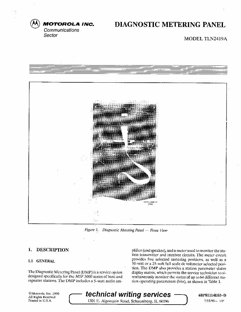
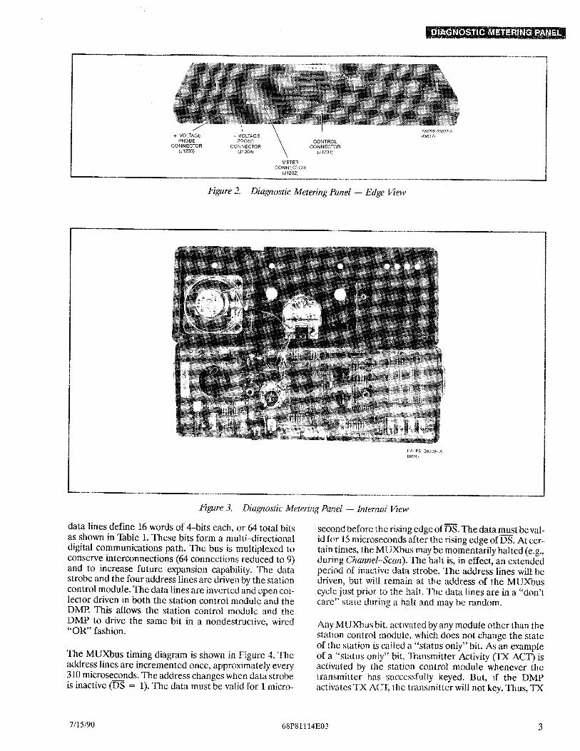
The DMP comes with a separate 40-conductor ribbon in-terface cable, a separate 8-conductor metering cable with"modular" connectors, two separate voltage probes anda set of housing rods that may be extended and insertedinto the mounting rails inside the station cabinet. Referto Figure 2 for the locations of the connectors used forthe CONTROL (11201), METER (11202), + voltageprobe (11203), and - voltage probe (11204). Refer toFigure 3 for a view of the DMP with its front panel re-moved.
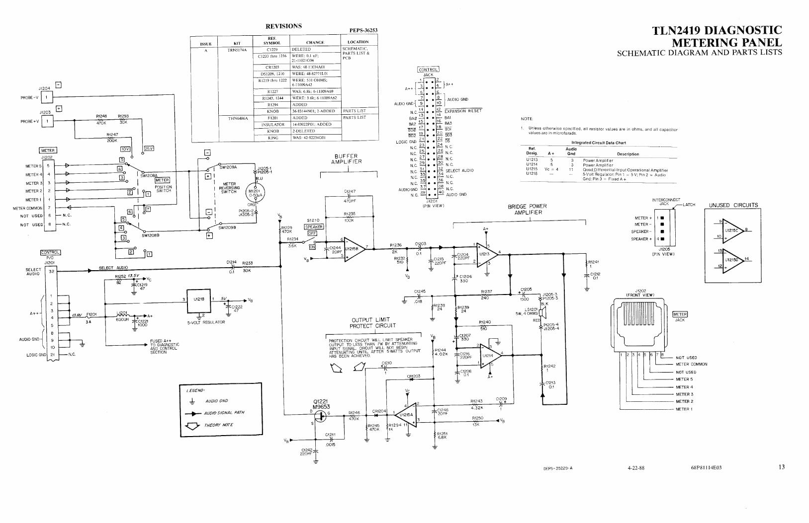
The 40-conductor interface cable connects the stationEXPANSION connector J800 (located on the top of thecontrol tray housing) to the DMP CONTROL connectorJ1201. This cable provides interface lines which connectpower, audio and digital signals between the station con-trol board, other control modules within the station, andthe DMP. There are four types of signal lines provided,as follows:•• audio line., dedicated logic line., multiplexed logic (MUXbus) lines., power and ground lines
2 68P81114E03
SELECT AUDIO (Pin 32) - Audio line
The Select Audio signal, originating on the station controlmodule, is the audio input for the local speaker amplifiercircuit in the DMP. Any of the following audio signals willbe present on the select audio line when it is properlygated by the control circuits in the station: primary receiv-er audio, secondary receiver audio, transmit audio fromthe remote wire line, and automatic station LD. andalarm tone audio. The Select.Andio line is connected tothe wiper of the VOLUMpcontrol on the control trayfront panel. Therefore, the debias level and ac level onthe line vary depending onthe VOLUME control setting.The DMP employs an audio power amplifier circuit toprovide up to 5watts of local service audio from the SelectAudio signal, through the DMP internal 4-ohm speaker.The audio power amplifier circuit can be disabled withSPEAKER ON/OFF switch S121O,located on the face ofthe DMP. By connecting an optional microphone(HMN1001) to CONTROL Jack J812 on the front panelof the station control tray, the transmitter can be locallykeyed and modulated, or intercom with the remote con-trol.console operator can be accomplished.
EXPANSION RE5ET (Pin 12) - Dedicated Logic line
11Ie.EXPANSION RESET signal is a shared logic linewhiChallows a clean, coordinated start up of the stationco:fltro1module and any other interconnected modules ore~t~rnal equipment (such as the DMP). The EXPAN-~QN RESET signal is active low at power-up, or whenstation control module switch S801 is put into the TESTposition, or when t~ station control module is reset byits watchdog timer circuit, or when another control mod-ule receives a command to reset the station. Also, normalMUXbus operation is suspended while the watchdog tim-er circuit generated RESET signal is active low. TheMUXbus data strobe line DS, is held inactive and theMUXbus address and data lines do not follow their nor-mal patterns.
IMPORTANTWhile the EXPANSION RESET line isactive low, no module except the stationcontrol module should write to the MUX-bus data lines. Otherwise, the station con-trol module may fail its self diagnostictests, and remain reset indefinitely.
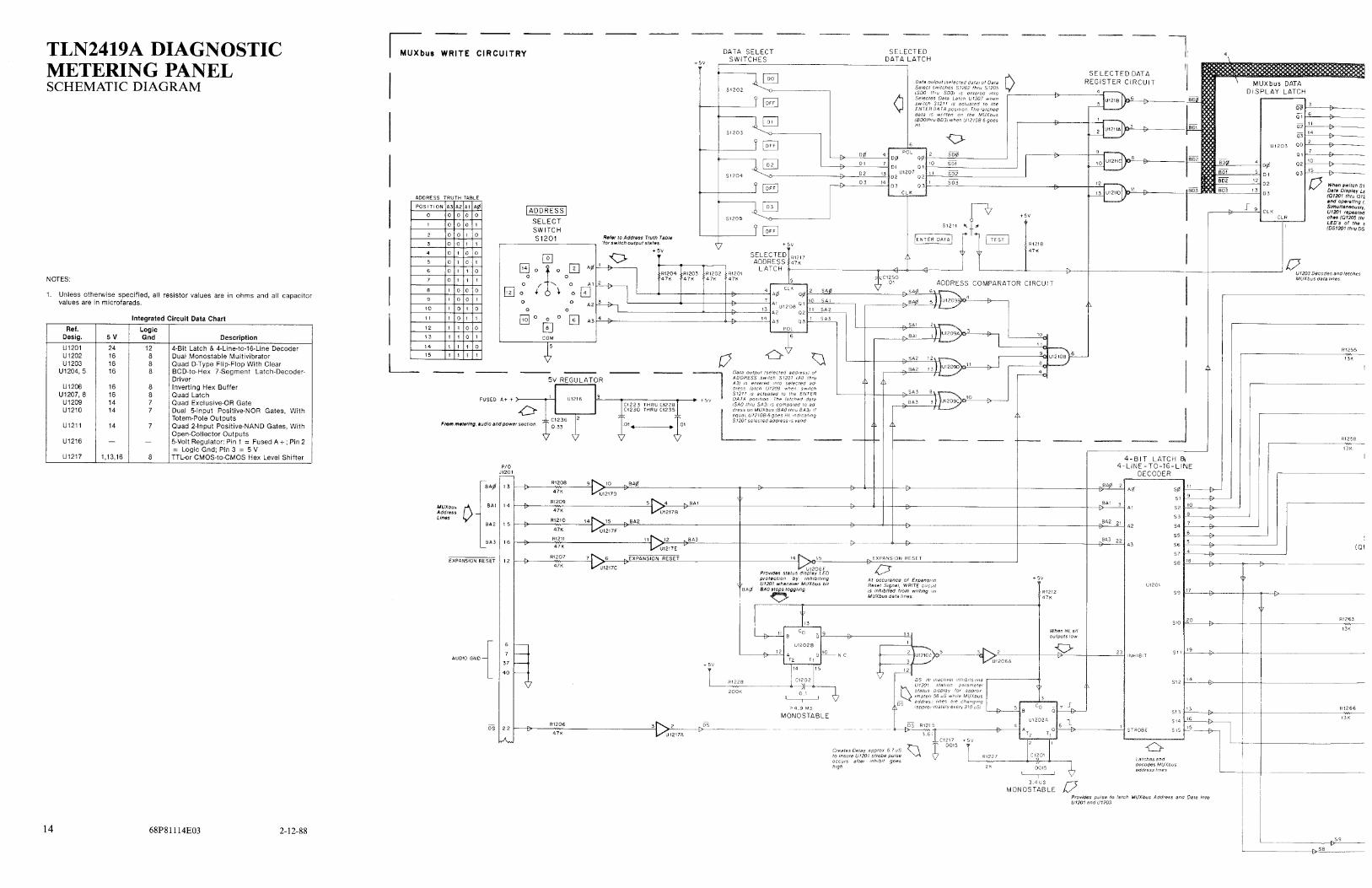
Multiplexed Logic (MUXbus) lines
The multiplexed logic (MUXbus) lines consist of the fol-lowing signals:
* Four Address lines (BAO-BA3) - Pins 13-16•• Four Data lines (BDO-BD3) - Pins 17-20•• Data strobe (DS) - Pin 22
All DMP MUXbus lines are referenced to audio ground(logic ground is not used). The four address and the four
7/15/90
METERCONNECTOR
(J1202)
Figure 2. Diagnostic Metering Panel - Edge View
FAEPS-36238-A(1624)
3. Diagnostic Metermg Panel - Internal View
data lines define 16words of 4~bits each, or 64 total bitsas shown in Table 1. These bits form a multi-directionaldigital communications path. The bus is multiplexed toconserve interconnections (64 connections reduced to 9)and to increase future expansion capability. The datastrobe and the four address lines are driven by thecontrol module. The data lines are.inverted and open col-lector driven in both the station control module and theDMP. This allows the station control module and theDMP to drive the same bit in a nondestructive, wired"OR" fashion.
The MUXbus timing diagram is shown in Figure 4. Theaddress lines are incremented once, approximately every310microseconds. The address changes when data strobeis inactive CDS = 1). The data must be valid for 1micro-
7/15/90
edge of DS. The data must be val-the rising edge of DS. At cer-
the MUXbus maybe momentarily halted (e.g.,halt is, in effect, an extended
strobe. The address lines will be",AllH,d\!, Uti, WIn remam at the address of the MUXbus
to the halt. The data lines are in a "don'ta halt and may be random.
any module other than thecontrol does not change the state
of the station is called a "status only" bit. As an exampleof a "status Transmitter Activity (IX ACT) isactivated station control module whenever thetransmitter keyed. But, if the DMPactivates TX the transmitter will not key. Thus, TX
68P81114E03 3
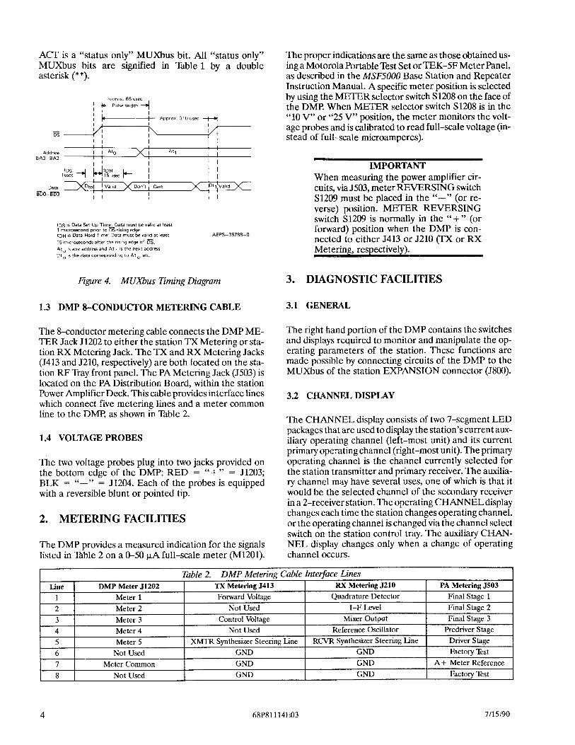
ACT is a "status only" MUXbus bit. All "status only"MUXbus bits are signified in Table 1 by a doubleasterisk (**).
Aoprox. 65 usee
I ~. Pulse Width ~I I
: ~ : Approx. 310 usee ~
55 ----tV: :'" i~I I I I I
i i A'o X i At, : :I I I I I
,~~~~ ~i~~secI+- : : :Data =:)(Dto! !Valid X Don't: ea,. X Ft':V"id ><=
iill1l-m53 I I I I I
AddressBAO-BA3
tos is Data Set Up Time: Data must be valid at least1 mi~rosecond prio~ to 1:5S rising edqetOH IS Data Hold Time: Data must be valid at least15 microseconds after the rising edge of 5S.Ato is any address and At 1 is the next addressDt 0 is the data corresponding to At 0' etc.
AEPS-35788-0
Figure 4. MUXbus Timing Diagram
1.3 DMP 8-CONDUCTOR METERING CABLE
The 8-conductor metering cable connects the DMP ME-TER Jack J1202 to either the station TX Metering or sta-tion RX Metering Jack. The TX and RX Metering Jacks(J413 and J21O, respectively) are both located on the sta-tion RF Tray front panel. The PAMetering Jack (J503) islocated on the PA Distribution Board, within the stationPower Amplifier Deck. This cable provides interface lineswhich connect five metering lines and a meter commonline to the DMP, as shown in Table 2.
1.4 VOLTAGE PROBES
The two voltage probes plug into two jacks provided onthe bottom edge of the DMP: RED = "+" = J1203;BLK = "-" = J1204. Each of the probes is equippedwith a reversible blunt or pointed tip.
2. METERING FACILITIES
The DMP provides a measured indication for the signalslisted in Table 2 on a 0-50 J.l.A full-scale meter (MI201).
The proper indications are the same as those obtained us-ing a Motorola Portable Test Set or TEK-5F Meter Panel,as described in the MSF5000 Base Station and RepeaterInstruction Manual. A specific meter position is selectedby using the METER selector switch S1208 on the face ofthe DMP. When METER selector switch S1208 is in the"10 V" or "25 V" position, the meter monitors the volt-age probes and is calibrated to read full-scale voltage (in-stead of full-scale microamperes).
IMPORTA.NTWhen measuringthe.power amplifier cir-cuits, via J503, meter REVERSING switchS1209 must be placed in the "-" (or re-verse) position. METER REVERSINGswitch S1209 is normally in the" +" (orforward) position when the DMP is con-nected to either J413 or J210 (TX or RXMetering, respectively).
3. DIAGNOSTIC FACILITIES
3.1 GENERAL
The right hand portion of the DMP contains the switchesand displays required to monitor and manipulate the op-erating parameters of the station. These functions aremade possible by connecting circuits of the DMP to theMUXbus of the station EXPANSION connector (J800).
3.2 CHANNEL DISPLAY
The CHANNEL display consists of two 7-segment LEDpackages that are used to display the station's current aux-iliary operating channel (left-most unit) and its currentprimary operating channel (right-most unit). The primaryoperating channel is the channel currently selected forthe station transmitter and primary receiver. The auxilia-ry channel may have several uses, one of which is that itwould be the selected channel of the secondary receiverin a 2-receiver station. The operating CHANNEL displaychanges each time the station changes operating channel,or the operating channel is changed via the channel selectswitch on the station control tray. The auxiliary CHAN-NEL display changes only when a change of operatingchannel occurs.
Table 2. DMP Metering Cable Interface LinesLine DMP Meter JI202 TX Metering J413 RX Metering J210 PA Metering J503
1 Meter 1 Forward Voltage Quadrature Detector Final Stage 1
2 Meter 2 Not Used I-F Level Final Stage 2
3 Meter 3 Control Voltage Mixer Output Final Stage 3
4 Meter 4 Not Used Reference Oscillator Predriver Stage
5 Meter 5 XMTR Synthesizer Steering Line RCVR Synthesizer Steering Line Driver Stage
6 Not Used GND GND Factory Test
7 Meter Common GND GND A + Meter Reference
8 Not Used GND GND Factory Test
4 68P81114E03 7/15/90
3.3 STATUS DISPLAY
The Station Parameter Status Display Matrix consists ofeight 8 element LED packages located behind the re-cessed sceened panel of the DMP. The screening identi-fies each of 641vlUXbus bits, via a specific mnemonic des-ignation, as shown in Thole 1.
The STATUS DisplaY.Pl"()vides a visible indication of themajor portion of the main control related activities thatare occurring at any timejn. the station. These include var-ious push-to-talk signals, the state of the squelch circuits,the presence of properly coded squelch signals, the sta-tion channel, the station-level alarms and "wild" cardfunctions, as well as specialized activities such as Chan-nel-Scan or DVP operation.
NOTETo check to see if all the LEDs in this sec-tion of DMP are functional, momentarilyswitch the ENIER DATA-TEST switch tothe TEST position. AU 64 LEDs in theSTATUS display area should light, and thetwo-digit CHANNEL display should indi-cate $FF.
The STATUS Display indicates the active control condi-tions within the station with a corresponding illuminatedLED. The absence of an expected condition can be readilyobserved as the station is operated, leading to rapid iden-tification of a defective area.
To simulate an active condition in the station using theDMP, select the address or row in the display containingthe particular signal with the ADDRESS switch. Next, setone of the data switches DO through D3 corresponding tothe column in the display containing the signal. Momen-tarily switch the ENTER DATA-TEST switch to the EN-TER DATA position and the condition will become ac-tive. To clear the condition, return the data switch to theOFF position and flip the switch to the ENTER DATAposition once again.
CAUTIONIt is recommended that the DMP be dis-connected from the control tray (via J8oo)during station power up. This prevents thestation from being initially activated in apossible undesirable function. However, ifthe station is powered up with the DMPconnected, and an undesirable conditiondoes occur, place the four DATA switchesto the OFF position, and then toggle theENTER DATA switch. This will deactivatethe four DMP data bits applied to theMUXbus Data Line and remove the unde-sirable condition
7/15/90 68P81114E03
DI~GNOSrrIC MErrEBING P~NEL.;
An active condition is also cleared when the ADDRESSswitch is moved to a different address, and the ENTERDATA switch is used to activate a MUXbus bit at the newaddress.
For example, suppose it is desired to verify that the properalarm tones would be sent by the station in the event ofa PA failure. To simulate this alarm condition using theDMP, set the ADDRESS switch to 12 (the row containingthe PA alarm signal) and flip the data switch up (for thecolumn containing this signal (D1). Flip the ENfERDATA switch, illuminating the LED in the status displayfor PA alarm and activating a simulated PA failure alarm.If the station is working properly, two beeps will be heard.
If the Dl switch is turned to the OFF position and the EN-TER DATA switch is activated, the PA alarm LED willtum off, and the alarm beeps will cease. Likewise, if theADDRESS switch is moved to address 1, and the D1switch is left in the up position, then when the ENTERDATA switch is activated, the PA alarm LED will turn off,the alarm beeps will cease, the LOCal PTf LED will illu-minate, and the station will key up.
NOTE"Status only" bits, when activated by theDMP, will cause their corresponding LEDto light, but will not affect a change in sta-tion operation. The station causes theseLEDs to light when it has successfully ac-complished a certain function.
4. MUXBUS BIT DEFINITIONS
4.1 INTRODUCTION
The following paragraphs provide definitions for each ofthe 64 operating parameters (MUXbus Bits) displayed bythe DMP. Each of these bits may have their state changedby the DMP. Each paragraph title gives the MUXbus Bitmnemonic, definition, and row-column address requiredfor access (in the form: #, D#), respectively.
4.2 SP XMIT (SPECIAL TRANSMIT) 0, D3
The SP XMIT bit indicates that the deviation and/or therf PA power should be either boosted or cut, defined byinformation in the station control module code plug. Thedefault condition in the station control module code plug,upon activation of this MUXbus bit, is deviation control.This bit will only have an effect during a PIT. The activa-tion of this bit, by itself, will not key the station.
4.3 SCAN (SCAN ENABLE) 0, D2
The SCAN bit forces the station control module to enablethe primary receiver as a scanning receiver. The stationmust be ordered with the Channel-Scan option in orderfor this feature to operate. Only the primary receiver canscan.
5
4.4 T ALM DS (TOTAL ALARM DISABLE) 0, Dl
The T ALM DS bit mutes all alarm tones until this bit isdeactivated. This bit will deactivate the station controlmodule alarm bits on the Reverse "Wild Card" bits 1through 4, but will not affect the other Reverse "WildCard" bits on the MUXbus. Pulsing T ALM DS for 25msec or longer will release S ALM DS, if active.
4.5 S ALM DS (SELECTIVE ALARM DISABLE) O,DO
The S ALM DS bit is meant to support a "nuisance avoid-ance" alarm feature. The console operator can mute in-progress alarm tones without fear of missing any newalarms. For example, initially all alarm bits (Reverse"Wild Card" bits, addresses 12 & 13) and S ALM DS areinactive. An alarm condition activates an alarm bit, andalarm tones are heard. The wireline control pulsesS ALM DS active for 25 msec or longer in response to aremote control console command, and the alarm tonesare muted. If the alarm condition were to disappear, thecorresponding alarm bit would be deactivated, S ALM DSwould be cleared, and no alarm tones would be heardsince no alarm bit is active. If, instead, a second alarm bitwere activated while the first alarm was active, S ALM DSwould be deactivated and alarm tones for both alarmswould be heard. The wireline control could re-enableS ALM DS, then alarm tones for both alarms would bemuted. S ALM DS does not deactivate the MUXbusalarm bits, but merely mutes the alarm tones.
4.6 RPT PTT (REPEATER PUSH-TO-TALK) 1, D3
The RPT PTT bit keys the transmitter, modulating withRX 1 Audio if no higher-priority PTT is active. If a high-er -priority PTT is active, the station control module deac-tivates RPT P1T. If the repeater PTT time-out timer(TOT) times out, RPT PTT will be deactivated, and thetransmitter will dekey. If repeater knock down (RPT KD)goes active while RPT PTT is active, RPT PTT will bedeactivated, PL reverse burst or DPL turn off code (RBITOC) will be encoded if appropriate, and the transmitterwill dekey. RPT PTT is active during repeater drop-outdelay. RPT PTT is inactive when RBITOC is encoded.The station control module turns on RPT P1T, if repeateraudio activity exists on Receiver 1, and if RPT KD is inac-tive, and if no higher-priority PTT is active. "Repeateraudio activity" is set for each channel by station controlmodule code plug qualifiers. These qualifiers determinewhat combination of the four MUXbus bits RX P L DS,Rl PL DT, RPT USQ, and AUX DET are ANDed to ob-tain RPT PTf. Line, Local, and Repeater PTT prioritiesare set for each channel by station control module codeplug qualifiers.
4.7 LIN PTT (LINE PUSH-TO-TALK) I,D2
The LIN PTT bit keys the transmitter, modulating withTX Audio (inbound wireline) if no higher-priority PTT is
6 68P81114E03
active. LIN PTT stays active if a higher-priority PTT is ac-tive. LIN PTT is inactive when RBITOC is encoded, un-less the RBITOC is caused by the Line PT T TOT timingout. If the station is so equipped, LIN PTT switches theantenna switch to its transmit state. Line, Local, and Re-peater PTT priorities are set for each channel by stationcontrol module code plug qualifiers
4.8 LOC PTT (LOCAL PVSH- TO-TALK) 1, Dl
The LOC PTT bit keys the transmitter, modulating withLocal Audio if no higher priority PTT is active. LOC PTTsays active if a higher priority PTT is active. LOC PTT isinactive when RBITOC is encoded, unless the RBIT OCis caused by the Local PTT TOT timing out. If the stationis so equipped, LO C PTT switches the antenna switch toits transmit state. LOC PTT is active if the PTT switch isdepressed on the local microphone plugged into the sta-tion control module front panel CONTROL connectorJ812. Line, Local, and Repeater PTT priorities are set foreach channel by station control module code plug qualifi-ers. The front panel XMIT switch on the station controlmodule will activate TX PL DS and key the station with-out activating the LOC PTT bit on the MUXbus. This keywill be without PL, DPL, or audio (silent carrier). Asthusly defined, it is not a true P1T, and can be overriddenby any other PTT
4.9 INTCOM (INTERCOM) 1, DO
The INTCOM bit is active if the remote control moduleINTERCOM switch is actuated. When INTCOM is ac-tive, the station control module treats LOC PTT as an In-tercom P1T. Local Audio is gated to the wireline (out-bound wireline) when a local PTT is generated, but thetransmitter is not keyed. When LOC PTT is not active,remote control console audio (inbound wireline) is gatedto the 112-watt local audio amplifier.
4.10 TX PL DS (TRANSMIT PLIDPL DISABLE) 2, D3
The TX PL DS bit mutes encoded PL or DPL. The Trans-mit PL Strip wireline option utilizes this bit. If PL or DPLis being encoded when TX PL DS goes active, then RBITOC will be generated before muting PL or DPL. Thisbit will also be set active whenever PLI DPL encoding isdisabled, such as during an auto ID transmission, or if thefront panel XMIT switch on station control module is ac-tivated.
4.11 TX ACT (TRANSMITTER ACTMTY) 2, D2
The TX ACT is a status only bit, and indicates that thetransmit rf channel (outbound) is ready. TX ACT goes ac-tive after a keyup, when the transmitter power output hasstabilized. In the event of a PA failure on keyup, TX ACTstays inactive (doesn't glitch). TX ACT goes inactivewhen the station control module dekeys the PA. TX ACTis inactive during RBITOC.
4.12 RX2 ACT (RECEIVER 2 ACTMTY) 2,mThe RX2 ACT bit indicates whether second receiver au-dio should be used. The second receiver control module
7/15/90
responds to an active RX2 ACT by gating deemphasized,PL-stripped audio from the second receiver to the RX2audio line. From there, it is mixed with line audio (out-bound wireline) by the station control module. RX2 Au-dio is also mixed with select audio (local speaker) by thestation control module.
4.13 RX1 ACT (RECEIVER 1 ACTMTY) 2, DO
The RXI ACT bit indicates whether the primary receiverhas audio present with the proper qualifiers to unmute re-ceiver audio. This condition is set for each channel by fourqualifiers in the station control module code plug. Thesequalifiers determine what combination of the four MUX-bus bits RX PL DS, Rl PL DT, Rl UN SQ, and AUX DETare ANDed to obtain RXI ACf. The station control mod-ule responds to an active RXI ACT by opening the RXIaudio gate. This gates RXI audio to both the line audio(outbound wireline) and select audio (local speaker) lines.RXI audio is also gated to the station control module re-peater audio gate. If the station is transmitting due to aRPT PTT, then the repeater audio gate will be open andRXI audio will be gated, via the IDC circuit, to the TXmodulation audio line.
4.14 RX PL DS (RECEIVE PLIDPL DISABLE) 3, D3
The RX PL DS bit causes the station to revert to carriersquelch only operation for purposes of determining statusof RXI ACT and RX2 ACf. The Monitor and ReceiverSquelch OnlOff wireline functions utilize RX PL DS.Also, the station control module front panel PL Disableswitch activates RX PL DS.
4.15 Rl PL DT (RECEIVER 1 PLlDPL DETECT) 3, D2
The Rl PL DT bit is active when PL or DPL codedsquelch is being detected via Receiver 1.
4.16 Rl SQ LV (RECEIVER 1 SQUELCH LEVEL) 3, nt
The R 1SQ LV bit changes the carrier squelch threshold.When Rl SQ LV is active, the primary receiver is operat-ing with "loose" squelch.
4.17 Rl UN SQ (RECEIVER 1 UNSQUELCH) 3, DO
The Rl UN SQ bit is a status only bit, and is active whenthe Receiver 1audio carrier squelch circuit on the stationcontrol module detects activity. Rl UN SQ is used for au-dio gating (refer to RX 1ACT), not for repeater keying(refer to RPT PIT).
4.18 R2 MUTE (RECEIVER 2 MUTE) 4, D3
The R2 MUfE bit causes the second receiver controlmodule to attenuate the audio driving the RX2 audio line,so that Local or RXI audio can be heard on both the line
7/15/90 68P81114E03
audio (outbound wireline) and select audio (local speak-er) lines. The attenuation is accomplished by means of apotentiometer on the second receiver control module.Therefore, RX2 audio can be fully muted, if desired.
4.19 R2 PL DT (RECEIVER 2 PLlDPL DETECT) 4, D2
The R2 PL DT is active when PL or DPL coded squelchis being detected via Receiver 2.
4.20 R2 SQ LV (RECEIVER 2 SQUELCH LEVEL) 4, D1
The R2 SQ LV bit changes the carrier squelch threshold.When R2 SQ LV is active, the second receiver is operat-ing with "loose" squelch.
4.21 R2 UN SQ (RECEIVER 2 UNSQUELCH) 4, DO
The R2 UN SQ bit is a status only bit, and is active whenthe Receiver 2 audio carrier squelch circuit on the secondreceiver control module detects activity. R2 UN SQ isused for audio gating (refer to RX2 ACT). The second re-ceiver can neither key the repeater (activate RPT PIT),nor modulate the transmitter.
4.22 GD TN DT (GUARD TONE DETECT) 5, D3
The GD TN DT bit becomes active whenever high levelguard tone is detected from the TX Audio signal (inboundwireline) by the tone remote control module. In stationswith an antenna switch, the station control module re-sponds to an active GD TN DT by switching the antennaswitch to its transmit state. The TX Audio signal is muted(on the station control module) while GD TN DT is ac-tive, in order to prevent remote control tones from beingtransmitted.
4.23 AUX DET (AUXILIARY DETECT) 5, D2
The AUX DET bit indicates that an optional decoder isdetecting. The optional decoder may be connected to ei-ther Receiver 1 or Receiver 2 audio. AUX DET can beused to activate TXl ACT , RX2 ACT, and RPT PIT ina manner similar to the Rl PL DT and Rl UN SQ qualifi-ers.
4.24 RPT KD (REPEATER KNOCK-DOWN) 5, Dl
The RPT KD bit disallows a repeater PTT. Also, this bitforces an existing active RPT PIT inactive.
4.25 RPT USQ (REPEATER UN SQUELCH) 5, DO
The RPT USQ bit is a status only bit, and is active whenthe Receiver 1repeater carrier squelch circuit, located onthe station control module, detects activity. This bit isused to key the repeater, not to gate audio (refer to RPTPTT).
7
4.26 ACC DIS (ACCESS DISABLE) 6, D3
The ACC DIS bit is a status only bit, and is active whenthe Access Disable station control module switch is actu-ated. ACC DIS active indicates that the following fivefunctions are inhibited: 1) Auto ID; 2) Alarm tones; 3)Time-out timers; 4) Repeater PIT initiated from the pri-mary receiver; and, 5) Wire line commands including LineP1T. When Access Disabled, the station operating chan-nel is selected with the CHANNEL select switch, locatedon the front panel of the remote control module. The pre-vious station operating channel is "remembered" by thestation control module and reinstated when the AccessDisable switch is deactivated. If there is no remote controlmodule connected as part of the station (repeater only op-eration) the DMP channel display will show $0, but thestation control module will equate this with Channell op-eration.
4.27 EX DA DT (EXTERNAL DATA DETECT) 6, D2
The EX DA DT bit, when active, can cause the stationcontrol module to mute TX, and/or local, and/or RXI(Repeater) audios, under code plug programming con-trol. This bit can allow or disallow selected mixing of theseaudios with TX data audio onto the TX modulation audioline. Which of the three audios is muted depends onwhich PTT is keying the transmitter. The intent is to op-tionally prevent audio from mixing with TX Data audio.Whether or not mixing occurs is determined by a qualifierfor each channel in the station control module code plug.
4.28 DW SEL (DIGITAL VOICE PROTECTIONSELECT) 6, Dl
The DVP SEL bit selects either the primary DVP code 1,or the secondary DVP subcode from the DVP controlmodule.
4.29 DW C/C (DIGITAL VOICE PROTECTIONCODED/CLEAR) 6, DO
The DVP C/C bit, when active, enables the encryptionand decryption functions of the DVP control module.Therefore, voice is transmitted "coded". When inactive,this bit disables the encryption and decryption functions.Therefore, voice is transmitted "clear".
4.30 ADDRESS 7, BITS 3 THRU 0 (RESERVED FORFUTURE USE) 7, D3 THRU 7, DO
These parameter bits are reserved for future applications,or special customer needs.
8 68P81114E03
4.31 TX RX C8, TX RX C4, TX RX C2, & TX RX Cl(TRANSMITTER/RECEIVER 1 CHANNEL)8, D3 TURU 8, DOandAUX C8, AUX C4, AUX C2, & AUX Cl(AUXILIARY CHANNEL) 9, D3 TURU 9, DO
These eight bits determine up to two sets of channels forthe station. A channel is a station state which chooses pre-defined groups of station parameters such as transmit andreceive frequencies and coded squelch code. The channelparameters are defined in the station control modulecode plug. Also, the station control module code plugcontains the transmit, primary receive, and Channel-Scanparameters. The (second receiver control module) codeplug contains the second receiver parameters. The TX/RX Channel occupies Address 8, Bits 3-0. The AuxiliaryChannel (Second Receiver and Channel-Scan) occupiesAddress 9, Bits 3-0. Optionally, the bits making up thetwo channels can be re-grouped to form two differentchannels, in which one channel has more. than four bits.In this optional configuration, the TX/RX Channel leastsignificant bit (LSB) is at Address 8, Bit O. If more thanfour bits are required to form the TX/RX channel repre-sentation, then those bits are taken from the auxiliarychannel assignments beginning with bit 0 of address 9.The Auxiliary Channel then starts (LSB) with the nextavailable bit after the last defined TX/RX channel bit andcontinues to bit 3 of address 9. If the two channels are tobe independent, then they cannot share any bits. Thismeans that the sum of the numbers of bits for the two in-dependent channels must be eight or less.
4.32 ADDRESSES 10 and 11, BITS 3 THRU 0(RESERVED FOR FUTURE USE)10, D3 THRU 10, DO and11, D3 TURU 11, DO
These parameter bits are reserved for future applicationsor special customer needs.
4.33 REVERSE "WILD CARD" PARAMETER BITS
Use of the reverse "wild card" bits (8 bits total, addresses12 & 13) requires the "wild card" module which residesin the Control Option Tray. The "wild card" inputs (fourper card) activate or deactivate the appropriate Reverse"wild card" MUXbus bit in response to a status signal ex-ternal to the station. The eight reverse "wild card" MUX-bus bits also have an additional definition. They are con-sidered alarms which, when activated, translate to alarmtones and are sent to the remote control console via theoutbound wireline. Optionally, the alarm tones may alsobe transmitted. The alarms are tone bursts (beeps). Thefour bits in Address 12 are normally defined as internalalarms and do not require the "wild card" equipment.Station conditions which the station control module mon-
7/15/90
itors cause the station control module to write to thesebits which, in tum, send the alarm tones.
NOTEIf the four internal alarm bits of address 12are activated by the DMP, or some othercontrol module connected to the MUX-bus, then the alarm beeps will be activated,but the actual internal alarm condition willnot be simulated. For example, if the PAFail alarm bit (RW2 PA) were to be acti-vated, two alarm beeps would be sent, butthe PA itself would not be forced to dekey.
The station control module code plug contains informationwhich determines whether an internal alarm gets written tothe MUXbus, and also if all of the reverse "wild card"MUXbus bits will be enabled to activate alarm tones. Thus,all 8 bits can be configured as external alarm inputs, if de-sired. The maximum number of internal alarms is four.
5. INTERNAL I EXTERNAL STATIONALARMS
5.1 INTERNAL STATION ALARMS
RW4 OVG (Reverse "Wild Card" Bit 4 - Bauery Overvol-taze) 12, D3
The RW4 OVG bit is the battery overvoltage internal sta-tion alarm parameter, and is activated by the station controlmodule. RW4 OVG is active when the station battery char-ger power supply indicates that the external (customersupplied) station emergency batteries are providing toomuch voltage (e.g., are overcharged).
RW3 SYN (Reverse "Wild Card" Bit 3 - Synthesizer Un-lock) 12, D2
The RW3 SYN bit is the transmit or primary receiver syn-thesizer unlocked internal station alarm parameter, and isactivated by the station control module. RW3 SYN is activewhen either the transmit, primary receive, or both synthesiz-ers are unlocked.
RW2 PA (Reverse "Wild Card" Bit 2 - PA Rlil) 12, Dl
The RW2 PA bit is the rf power amplifier fail internal stationalarm parameter, and is activated by the station controlmodule. RW2 PA is active when the rf power amplifier has
DIAGNOSTIC METERING PANEL.
failed. A successful keyup or a station control module resetis required to clear the alarm. The alarm may be active whenthe transmitter is de-keyed, due to a prior failure. PA Failmeans that one or both of the station control module PAstatus lines (pA On or PA Full Power) are inactive 30-45msec after the start of a keyup, or for 30-45 msec continu-ously during keyup, thereafter. RW2 PA is not activated bythe station control module if the PA is not keyed at full pow-er due to the station control module personality EPROMrf power cut option. If the station control module servicejumper (JUB01) is installed, the station control module willactivate RW2 PA regardless of the PA status lines. This isa reminder that the rf power amplifier is operating in a non-standard manner.
RWl BAT (Reverse "Wild Card" Bit 1 - Bauery Revert) 12,DO
This bit is the battery revert internal station alarm parame-ter activated by the station control module. RWI BAT is ac-tive when the station battery charger power supply indicatesthat the station has lost ac power and has switched to emer-gency battery backup. RWI BAT becomes inactive as soonas proper ac power is restored to the station.
5.2 EXTERNAL STATION ALARMS
RWC 5, RWC 6, RWC 7, & RWC 8(Reverse "Wild Card" Bits 5 thru 8)13, D3 thru 13, DO
Reserved for those reverse "wild card" applications whichprovide an interface between external station inputs and theMUXbus. These parameters can also provide additionalalarm input capability thru information contained in the sta-tion control module code plug, which allows these bits to beidentified as alarm inputs.
5.3 FORWARD "WILD CARD" PARAMETER BITS
FWC 1, FWC 2, FWC 3 & FWC 4(14, D3 THRU 14, DO) andFWC 5, FWC 6, FWC 7, & FWC 8(15, D3 THRU D, DO)
Use of the Forward "Wild Card" bits (up to 8 bits on ad-dresses 14 & 15) require the "wild card" module (four out-puts per card) which resides in the Control Option Tray. Re-mote wireline control activates these bits. The "wild card"control module responds by activating a relay closure or anopen collector output. These closures and/or outputs canthen be used to control equipment external to the station.
COMPUTER SOfTWARE COPYRIGHTS
The Motorola products described in this instruction manual may include copyrighted Motorola computer programs stored in semiconductormemories or other media. Laws in the United States and other countries preserve for Motorola certain exclusive rights for copyrighted computerprograms, including the exclusive right to copy or reproduce in any form the copyrighted computer program. Accordingly, any copyrightedMotorola computer programs contained in the Motorola products described in his instruction manual may not be copied or reproduced in anymanner without the express written permission of Motorola. Furthermore. the purchase of Motorola products shall not be deemed to grant eitherdirectly or by implication. estoppel. or otherwise, any license under the copyrights. patents. or patent applications of Motorola. except tor thenormal non-exclusive, royalty free license to use that arises by operation of law in the sale of a product.
7/15/90 68P81114E03
EPS-34440-B
9
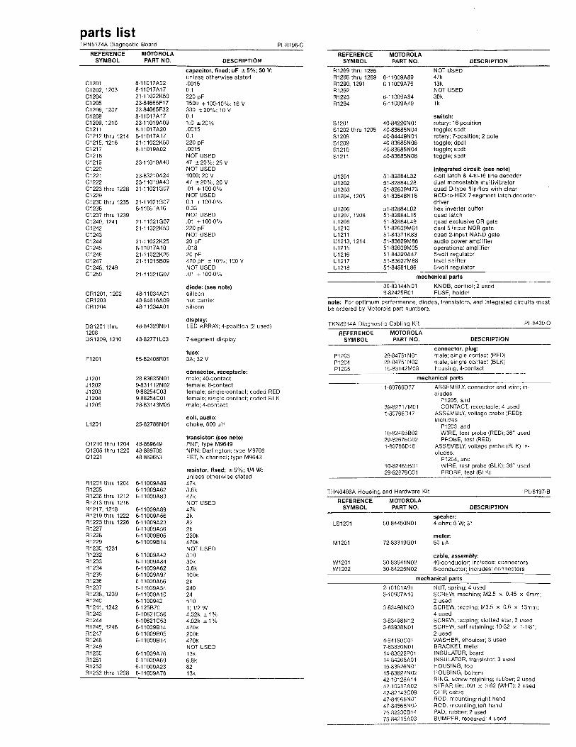
parts listTRN5174A Diagnostic Board PL-8196'C
REFERENCE MOTOROLASYMBOL PART NO. DESCRIPTION
capacitor, fixed; uF ± 5%; 50 V:unless otherwise stated
C1201 8·11017A02 .0015C1202, 1203 8·11017A17 0.1C1204 21·11022K50 220 pFC1205 23-84665F17 1500 + 100·10%; 16 VC1206, 1207 23-84665F32 330 ± 20%; 10 VC1208 8·11017A17 0.1C1209, 1210 23·11019A09 1.0 ±20%C1211 8·11017A20 .0015C1212 thru 1214 8·11017A17 0.1C1215, 1216 21·11022K50 220 pFC1217 8·11019A02 .0015C1218 NOT USEDC1219 23-11019MO 47 ±20%; 25 VC1220 NOT USEDC1221 23-83210A24 1000;20VC1222 23-11019MO 47 ± 20%; 20 VC1223 thru 1228 21-11021G07 .01 + 100·0%C1229 NOT USEDC1230 thru 1235 21·11021G07 0.1 +100-0%C1236 8-11051A16 0.33C1237 thru 1239 NOT USEDC1240, 1241 21-11021G07 .01 + 100·0%C1242 21-11022K50 220 pFC1243 NOT USEDC1244 21-11022K25 20 pFC1245 8-11017A10 .018C1246 2H1022K25 20 pFC1247 21·11015809 470 pF ± 10%; 100 VC1248, 1249 NOT USEDC1250 21·11021G07 .01 +100·0%
diode: (see nole)CR1201,1202 48-11034A01 siliconCR1203 48-84616A09 hot carrierCR1204 48·11034A01 silicon
display:DS1201 thru 48-84329N01 lED ARRAY; 4-position (2 used)1208DS1209, 1210 48·82771 l03 7-segment display
luse:F1201 65·82408R01 3A; 32 V
connector, receptacle:J1201 28·83835N01 male; 40·contactJ1202 9·831112N02 female; 8·contactJ1203 9·88254C03 female; slnqle-contact: coded REDJ1204 9·88254C01 female; single-contact; coded BlKJ1205 28·83143M05 male; 4·contact
coil, audio:l1201 25·82786N01 choke, 600 uH
transistor: (see note)01210 thru 1204 48-869649 PN P; type M964901205 thru 1220 48·869706 NPN; Darlington; type M970601221 48-869653 FET, N-channel; type M9643
resistor, fixed; ± 5%; 114W:unless otherwise stated
R1201 thru 1204 6·11009A89 47kR1205 6·11009A62 3.6kR1206 thru 1212 6·11009A89 47kR1213 thru 1216 NOT USEDR1217,1218 6·11009A89 47kR1219 thru 1222 6·11009A56 2kR1223 thru 1226 6·11009A23 82R1227 6·11009A56 2kR1228 6·11009805 220kR1229 6·11009814 470kR1230, 1231 NOT USEDR1232 6·11009M2 510R1233 6-11009A84 30kR1234 6-11009A62 3.6kR1235 6-11009A97 100kR1236 6-11009A56 2kR1237 6-11009A34 240R1238,1239 6·11009A10 24R1240 6·1100942 510R1241,1242 6·125870 1;1/2WR1243 6-10621C56 4.32k ± 1%R1244 6·10621C53 4.02k ± 1%R1245, 1246 6-11009814 470kR1247 6-11009805 200kR1248 6·11009814 470kR1249 NOT USEDR1250 6·11009A76 13kR1251 6·11009A69 6.8kR1252 6·11009A23 82R1253 thru 1268 6-11009A76 13k
REFERENCE MOTOROLASYMBOl PART NO_ D~SCRIPTION
R1269 thru 1285R1286 thru 1289 6-11009A89R1290, 1291 6-11009A76R1292R1293 6-11009A84R1294 6·11009A49
S1201S1202 thru 1205S1208S1209S1210S1211
U1201U1202U1203U1204,1205
U1206U1207, 1208U1209U1210U1211U1213,1214U1215U1216U1217U1218
40-84226N0140-83685N0440-84449N0140·83685N0640-83685N0440-83685N08
51-82884l3251-82884 L2851-82609M7351-83548N18
51-82884 l0251-82884l1551-82884L4951-82609M6151-84371 K8351-83629M8651-82609M0551-84320A4751-83627M8851-84561 L86
NOT USED47k13kNOT USED30k1k
switch:rotary: 16-positiontoggle; spdtrotary; 7-position; 2 poletoggle; dpdttoggle; spdttoggle; spdt
integrated circuit: (see nole)4-bit latch & 4-to-16 line decoderdual monostable multivibratorquad D-type tllp-flop with clearBCD-to-HEX 7-segment latch-decoder-driverhex inverter bufferquad latchquad exclusiveOft gatedual 5-input NOH gatequad 2-input NAND gateaudio power amplifieroperational amplifier5-voll regulatorlevel shifter5-volt regulator
mechanical parts
36-83144N01 KNOB, control; 2 used9-82425R01 FUSE, holder
note: For optimum performance, diodes, transistors, and integrated circuits mustbe ordered by Motorola part numbers.
TKN8914A Diagnostic Cabling Kit PL·8430-0
REFERENCE MOTOROLASYMBOL PART NO. DeSCRIPTION
P1203P1204P1205
28-84751 N0128-84751 N0215-83142M08
connector, plug:male; sinqle contact (RED)
single contact (8lK)4-contact
1·80766D37
39-82717MOI1-80766047
10-8246580229-82676C021-80766D48
10-8246580129-82676COI
receptacle; 4 used(RED);
includes
eludes:P1204,WIRE,PROBE,
36" used
THN6486A and Hardware Kit Pl-8197-8
SYMBOL PART NO. DESCRIPTION
lS1201
M1201
W1201W1202
speaker:50-84450N01 4 ohm; 5 W; 3"
meter:72-83319GOI 50 uA
cable, assembly:30-83941 N02 40-conductor; includes: connectors30-84225N02 8-conductor;includes: connectors
mechanical paris
2·10101A913-10907A10
3-83498N03
3-83498N123·83938N01
4-84180C017-83830N0114-83022POl14-84268AOI15-83826N0115-83827N0242-10128A1442-10217 A0242-82143C0947-84568N0147-84568N0275·82230B 1475-84215A03
NUT, spring; 4 usedSCREW, machine; M2.5 x 0.45 X 6mm;2 usedSCREW, tapping; M3.5 x 0.6 x 13mm;4 usedSCREW, tapping; slotted star; 3 usedSCREW, self retaining; 10-32 x 1-1/8";2 usedWASH ER, shoulder; 3 usedBRACKET, meterINSULATOR, boardINSULATOR, transistor; 3 usedHOUSING, topHOUSING, bottomRING, screw retaining; rubber; 2 usedSTRAp, tie; .091 X 3.62 (WHT); 2 used
cablemounting; right handmounting; left handrubber; 2 used
4 used
JI204 BPROBE-V
JI203 ElPROBE-t-V
ICONTROLIPIO
Jt201
SELECT 32AUDIO
H'~
2
3
4
5
AUDIO GND{
8
9
10
LOGIC GND 21
Rt248 RI293
470K 30K
RI247
200K
~ ffi]
REVISIONSPEPS-36253
REEISSUE KIT SYMBOL CHANGE LOCATION
A TRN5174A C1229 DELETED SCHEMATIC,
CI233 thru 1236 WERE: 0.1 uF;PARTS LIST &
21-11021G04PCB
CR1203 WAS: 48-1 1034AOI
DS1209, 1210 WERE: 48-82771LOI
R1219 thru 1222 WERE: 510 OHMS;6-11009A42
R1227 WAS: 6.8k; 6-1 1009A69
R1243, 1244 WERE: 3.6k; 6-1 1009A62
R1294 ADDED
KNOB 36-83144NOl; 2-ADDED PARTS LIST
THN6486A F1201 ADDED PARTS LIST
INSULATOR 14-83022POl; ADDED
KNOB 2-DELETED
RING WAS: 42-82234GOI
0.1 30K
B
I SW1209A
811 METERI REVERSING
1SWITCH
I[]I
1ISWI209B
EJ
BUFFERAMPLIFIER
I
CI247
lOOK
r SWi20BAI IMETER IPOSITIONSWITCH
OJl--~-----------;:-'470PF
RI235
51210
ISPEAKER IffiJSWi208B
CI214 RI233
RI229470K
RI234
7
RI241I
3.6K
SELECT AUDIO
1--_-+-~/3~.8~V'__'\.FI:.=2:=0:.1_ .•••._~L~12~O~I::-..,.:-'"+ ..•.A+3A 600UH ICI221
1000
N,C.
FUSED A++1-- -+ TO DIAGNOSTIC
AND CONTROLSECTION
3 UI218 5V VB
+±CI22247
-::1:-25-VOLT REGULATOR
-::1:- AUDIO GNo
--..- AUDIO SIGNAL PATH
-Q THEORY NOTE
OUTPUT LIMITPROTECT CIRCUIT
I
I CONTROL IJACK
1 .2• }A++3 • .4• • 6
7 • • 8 } AUDIO GNDAUDIO GND{ 9 • • 10
N.C. II •• 12 EXPANSION RESET
BAlli 13 •• 14 BAI
BA2 15 •• 16 BA3
~ 17 •• 18 B5Itlm 19 • • 20 BD3
LOGIC GND 21 • 22 OSN_C. 23 •• 24 N.C
N.C. 25 •• 26 N. C.
N.C. 27 •• 28 N. C.
N.C. 29 •• 30 N. C.
N C. 31 • • 32 SELECT AUDIO
N:C. 33 " • 34 N.C.
N.C. 35 •• 36 N.C.
AUDIO GND 37 • • 38 N.C.N. C. 39 • • 40 AUDIO GND
JI201lPIN VIEW)
RI236 CI203
2K
RI232510
0.1CI215
1220PF
CI245
f .~B
NOTE:
TLN2419 DIAGNOSTICMETERING PANEL
SCHEMATIC DIAGRAM AND PARTS LISTS
1. Unless otherwise specified, all resistor values are in ohms. and all capacitorvalues are in microfarads.
_--::-c:- -----'I...n,,'e:=gratedCircui~'O-"-~~h-"_r' ~~_Ref. Audio
Desig. A + Gnd Description
U1213 5 3 Power AmplifierU1214 5 3 Power AmplifierU1215 Vc = 4 11 OuadDiffere ntial-Input Operational AmplifierU1218 5-Volt Regulator: Pin 1 = 5 V; Pin 2 = Audio
Gnd; Pin 3 = Fixed A +~----
BRIDGE POWERAMPLIFIER
!
INTERCONNECTJACK LATCH
4
Cf205
+f5~ .• ~~II~~~--~BLK
LSI2015W, 4 OHMS
REDP1205-4Jf205-4
I METER IJI202
METER 5 5
METER 4 4
METER 3 3
METER 2 2
METER I
METER COMMON 7
NOT USED 6 N.C.
NOT USED 8 N.C.
METER + f!lllMETER - IIIi
SPEAKER - IiII
SPEAKER + 4 l1li
RI23824
PROTECTION CIRCUIT WILL LIMIT SPEAKEROUTPUT TO LESS THAN 7W BY ATTENUATINGINPUT SIGNAL. CIRCUIT WILL NOT BEGINATTENUATING UNTIL AFTER 5WATTS OUTPUTHAS BEEN ACHIEVED.
./'f CI210~1_-2-+II----~
CRf203
01221M9653
D G RI246 CRI204
470KS
RI245470K
C1211
VB -e- -=.0015
C1242220PFI
A+
RI237
240
RI23924
RI2444.02K
1+ 5
CI20BJ 0.1 A+
RI243C1209
+
CI2464.32K
20PFRI250
VB13K
4
Rf242I
DEPS-35229-A
CI2130.1
JI205(PIN VIEW)
J1202lFRONT VIEW)
,J ~
I 2 3 4 5 6C
IMETERIJACK
NOT USED
METER COMMON
NOT USED
METER 5
METER 4
METER 3
METER 2
METER 1
4-22-88 68P81114E03
UNUSED CIRCUITS
13
r-::bUS WRITE CIRCUITRYTLN2419A DIAGNOSTICMETERING PANELSCHEMATIC DIAGRAM
NOTES:
I
IADDRESS TRUTH TABLE
IPQS I T I ON A3 A2 AI Art
0 o a 0 0
o 0 0 I
0 0 I 0
I0 o I
o I o aa I 0 I
a I I a
Ia I I
I a a aI a a I
10 I a I a
III I a I
12 100
13 I I 0 I
14 I I I a
L 15 I I I I
1. Unless otherwise specified, all resistor values are in ohms and ali capacitorvalues are in microfarads.
Integrated Circuii Data Chart
Ref. LogicDesig. 5V Gnd Description
U1201 24 12 4-Bit Latch & 4·Line·to·16·Line DecoderU1202 16 8 Dual Monostable MultivibratorU1203 16 8 Quad D-Type Flip-Flop With Clear
U1204, 5 16 8 BCD-to-Hex 7-Segment Latch-Decoder-Driver
U1206 16 8 Inverting Hex BufferU1207, 8 16 8 Quad LatchU1209 14 7 Quad Exclusive-OR GateU1210 14 7 Dual 5-lnput Positive-NOR Gates, With
Totem-Pole OutputsU1211 14 7 Quad 2-lnput Positive-NAND Gates, With
Open-Coli ector OutputsU1216 - - 5-Volt RegUlator: Pin 1 = Fused A +; Pin 2
= Logic Gnd; Pin 3 = 5 VU1217 1,13,16 8 TTL-or CMOS-to-CMOS Hex Level Shifter
IADDRESS I
SELECTSWITCHS1201
DATA SELECT
+5V SWITCHES
S 1202
~
~I S1203
I B~
S 1204
~[D2J
51205
BRefer to Address Truth Table'for switch output states. + 5V
+ 5V0-RI204 RIZ03 RIZ0247K 47K 47K
SELECTEDDATA LATCH
60-
o¢ POL sOjj00 o¢
01 ID SOl01 01
02 13 U1207 II S0202 02
03 I.03 03
SD3
eLK
+5V
Bo
IT] A01-''-£>---oo A I 20[;]
SELECTED DATAREGISTER CIRCUIT
U1Z03
O¢01
1202
1303
I9 eLKeLR
o
EJoo 0 A2
0
0 0 0 A3 4
[8]COM
5
o
~o
SA3
FUSEDA+ + >---~'-1 BA3 U1209C:»,,1O'------B~-
From mo,,,lng, euato and power section.
U1Z18I JO"----!'l~-----''''''-
Ul211AIj!)"----!'l~----f!""-
Whon swlfch S1Dat« Display LIl(Q1201 thru Q1;'ena operatlnQ (,Simultaneously,U1201 (1.lp&0IedChf§S (01205 tnrLED's of the s(D$1201 thru D$
i5?l- 601
02II
0314
00
011-'--~[O>-----
Q2 10
031-'-"5'--[0>----_o
R1255
13K
I
4- BIT LATC H B\ JJ4- LINE - TO-16- LINEDECODER
SAA0 5¢
II
51SAl 3 10AI S2
53SA2 21 54A2
S58A3 22
A3 S6
S7
58 18
U1201
59 17
20 RI263SID
13K
23 51jINHI BIT
+ SV
R121247K
,,,,,.o {U12028 -012 Q 10
37
40
I>4.9 MS
MONOSTABLELR1206 D5
OS 2247K U1217A
PIOJ1201
rR1208 10 SA¢1347K U1217D
14R1209 BAI
MUXlw/> o B8AA~Address 47K U12178Lines Rt210 14 IS BA215
47K U1217F
RI211 11 12 BA3 t>-BA3 1647K U1217E
R1207 EXPANSION RESET 14 15 EXPANSION RESETEXPANSION RESET 12
047K U1217C
14 68P81114E03 2-12-88
3.4
MONOSTABLElelch MUXbus
Rt266
and into

SE LECTED DATAREGISTER CIRCUITleered data} of Dala ~
s $1202 thru 51205 V3) is entered into r--~~~~----B>-~~~---"--r-")i~a~c:'u~::~7fOW~~~ U121B1)c"'---;:>-~~~--!!l1l!.osition. The/archedn on the MUXbusvnen U1210B·6 goes
01 10 Ul211C lO''--t>-~~~~
12
+5V
R121847K
09~"-~-t>-~___,
RESS COMPARATOR CIRCUIT
09C;'JC>,,,,0~--£;>---l
13 U12110 »"-'-'-t>-~~~_~~
J4-81T LATCH SO
4- LINE - TO -16- LINEDECODER
SAA~ 8¢
11
81SAl 3 10Al 82
83BA2 21 A2 84
85BA3 22
A3 86
87
8B IB
Qi3r--+----------------------------------------+------------Qll--"-~__j)>-~~~~~~~~~~~~~~~~~~~~~~~~~~~~~~~~~~~~~~~~~~~~~-+-------------,Q2 11
Q3 14
QOfL-__j)>-----------------------------------------------,Ql!--!--__j)>--------------~-----------------------___,02 10
Q3 15
[}
LED 5-VOLTSWITCHES
(Q1201-QI204)
R1222
U1203
O¢
0112
0213
03
S 9 ClKClR
When .wltch S1211 Ja actuated to TEST position, MUXbu' ~Dat. Display Latch U1203 forces 811LED 5-voft swItches(01201 thru Q12CU) on, lind causes thct auxiliary (DS1210)and o".,atlng (DS1209) channel displays to Indlc,t. $F.SimultaneouSly, 4-blt 'slch & 4·Lln8-fo-16-Llne Decod.,U120f fePHt&dly ripples through the LED ground swit-ch •• (01205 th,u QI220). Theso two actfons ceuse all 64 0LED's of the station parameter status display matrix(D51201 thru 051208) to light. R1223
82Rt22482
R122582
Q1202M9649
Q1203M9649
Q1201M9649 RI221R1219 RI220
2K 2K2K2K
oU1203 Decodes and latchesMUXbus data lines
R1253
13K
R1255
13K Q1207M9706
R1256
13K
R1258
13K Q1210M9706
R1259
13K
R1260
13K
LEDGROUND
SWITCHES(Q1205 - Q1220)
17015
R1261
13K
R1263
13K Q1215M9706
Provides pulse to latch AWXbus Addrfflss end Data IntoU1201sndU1203.
R1264
13K
R1266
R1267
Latches anddecodes MUXbusaddress lines
13K Q1218M9706
13K
R1268
13K
STATION PARAMETER STATUS DI SPLAY MATRIX
89
Q1204M9649
4
+5V
RI28947K
88
R122682
10 9 6 5
03 02 0\ O¢
UI204
PfOJ120!
17
'"J18 SOl ¢ IAUXbu.O.t.•
19 '802 Un.!20 803
ABCOEFG
12 13 14 15 1 2 3
10985423
ABCoEFG
~_A~_
COM
DS12iOAUXILIARYCHANNELDISPLAY
+5VU1201
RI212 89 17
47K
810 20
When HI, alloutputs low
0 23 811 19INHIBIT
U1206A
14
3
CD 7 I 13Q 813
U1202A 1- 814 16
STROBE 15
+ 5V
CR120!
R1290
13K
CLOCKPULSE
C1240.01
II 89
., 12
I U1206E
11
89
Clock Pulse generatingCircuit used to latch auxiliary channel numberdata into U1204, SeeChannel Display TimingDiagram
R128847K
R12B747K
R12864':"K
6 5
ABC' 0 E F G
12 13 \4 15 1 2 3
03 C2 01 o¢
U1205
COM
+ 5V
CR1202
I!
R1291
13K
CLOCKPULSE
C1241.01
88
10
U1206D
J88
LEGEND:
THEORY NOTE
LOGIC GND
---&>-- CONTROL SIGNAL
BCD-TO- HEX7-SEGMENT
LATCH-DECODER -DRIVER
CHANNEL DISPLAY TIMING DIAGRAM
I I
S80RS9~- - ISB OR 89LLs--
ClOCK~~.PULSE' V!
I !I' I
LOAD LATCHDS1209 DATA DATA
OPERATINGCHANNELDISPLAY
UNUSED CIRCUITS
~ " U12068
7"'--.6~
Clock Pulse generating circuitu,sedto latch operating Channel numberdata into U1205, See Channel DisplayTiming Diagram
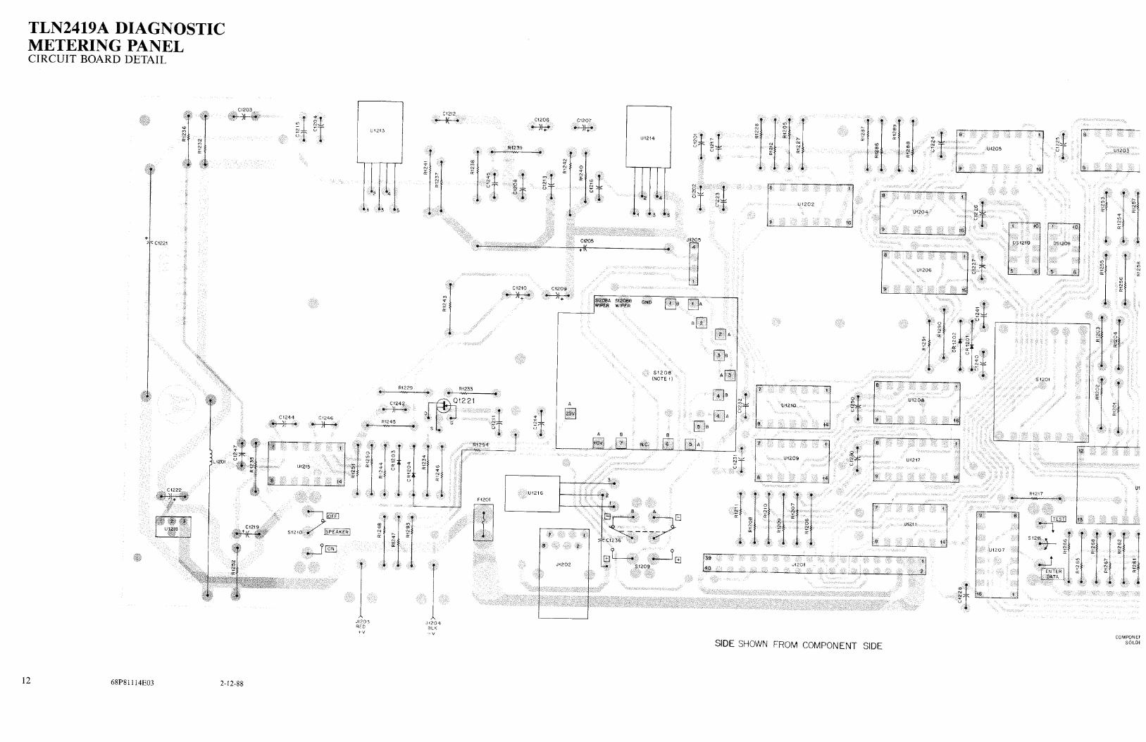
TLN2419A DIAGNOSTICMETERING PANELCIRCUIT BOARD DETAIL
C1206 C1207.....jf-:;:<> .. ~~.
UI214
ui213
C1221 CI205+
+
51208(NOTE I)
J1204BLK-v
SIDE SHOWN FROM COMPON ENT SIDECOMPONEI
SOLD!
12 68P81114E03 2-12-88
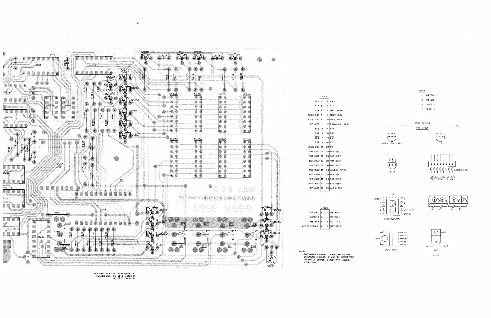
COMPONENT SIDESOLDER SIDE
BD-EEPSBD-EEPS -36182-BOL_EEPS-36183-B
-36184- B
A++
A++ 3
A++ 5
AUDIO GND 7
AUDIO GND 9
NOT USED 11
BAIll 13
BA2 15
BDIll 17
BD2 19
LOGIC GND 21
NOT USED 23
NOT USED 25
NOT USED 27
NOT USED 29
NOT USED 31
NOT USED 33
NOT USED 35
AUDIO GND 37
NOT USED 39
RESET
16 BA3
18 SOl
C B E
UQ1201 THRU Q122020 BD3
22 OS
24 NOT USED
26 NOT USED
28 NOT USED
30 NOT USED
32 SELECT AUDIO
34 NOT USED
36 NOT USED
38 NOT USED
40 AUDIO GND
o I-Z Z :::>
~3 2 1
U1218
METER 1OJ12022 METER
METER 3 3 4 METER 4
METER 5 5METER COM 6 NOT USED
MON 7 8 NOT USED
DS1209.DS1210
§[JA+
GND0 4 OUT3 GND2 IN-1 IN+
U1213.U1214NOTES'
L THE BOXEDSCHEMATIC ~,~~BERS CORRESPONDTO SWITCH RAM.•••••• AND "a" TO THERESPECTIV~yEGMENT S120SA AND CORRESPOND. S1208S.
mJI2105METER +
2 METER-
3 SPKR-
4 SPKR +
BASE ~ETAILS
TOP VIEWS
~Q1221
(K)
051201 TH(SEE DETAI~U 051208SELOW)
NOT USED
COM K
~
GND
I 2 3
IN OUT
GND
UI216