MOS operational amplifier design-a tutorial overvie · Schematic of basic two-stage CMOS...
14
IEEE JOURNAL OF SOLID-STATE CIRCUITS, VOL. SC-17, NO. 6, DECEMBER 1982 969 , Special Papers MOS Operational Amplifier Design— A Tutorial Overview PAUL R. GRAY, FELLOW, IEEE, AND ROBERT G. MEYER, FELLOW, IEEE (ZnvitedPaper) Abstract-This paper presents an overview of current design tech- niques for operational amplifiers implemented in CMOS and NMOS technology at a tutorial level. Primary emphasis is placed on CMOS amplifiers because of their more widespread use. Factors affecting volt- age gain, input ,noise, offsets, common mode and power supply rejec- tion, power dissipation, and transient response are considered for the traditional bipolar-derived two-stage architecture. Alternative circuit approaches for optimization of particular performance aapects are sum- marized, and examples are given. I. INTRODUCTION T HE rapid increase in chip complexity which has occurred over the past few years has created the need to implement complete analog-digital subsystems on the same integrated cir- cuit using the same technology. For this reason, implementa- tion of analog functions in MOS technology has become in- creasingly important, and great strides have been made in recent years in implementing functions such as high-speed DAC’S, sampled data analog filters, voltage references, instru- mentation amplifiers, and ‘so forth in CMOS and NMOS tech- nology [1] . These developments have been well documented in the literature. Another key technical development has been a maturing of the state of the art in the implementation of op- erational amplifiers (op amps) in MOS technology. These am- plifiers are key elements of most analog subsystems, particu- larly in switched capacitor filters, and the performance of many systems is strongly influenced by op amp performance. Many of the developments in MOS operational amplifier de- sign have not been as well documented in the literature, and the intent of this paper is to review the state of the art in this field. This paper is focused on the design of op amps for use within single-chip analog-digital LSI systems, and the particu- lar problems of the design of stand-alone CMOS amplifiers are not addressed. Manuscript received August 24, 1982; revised September 27, 1982. This work was supported by the Joint Services Electronics Program under Contract F49620-79-c-0178 and the National Science Founda- tion under Grant ENG79-07055. The authors are with the Department of Electrical Engineering and Computer Sciences and the Electronics Research Laboratory, Univer- sity of California, Berkeley, CA 94720. In Section II, the important performance requirements and objectives for operational amplifiers within a monolithic ana- log subsystem are summarized. In Section III, the perfor- mance of the basic two-stage CMOS operational amplifier architecture is summarized. In Section IV, alternative circuit approaches for the improvement of particular performance as- pects are considered. In Section V, the particular problems associated with NMOS depletion load amplifier design are con- sidered, and in Section VI, the design of output stages is con- sidered. Finally, a summary and discussion of the design of amplifiers in scaled technologies are presented in Section VII. II. PERFORMANCE OBJECTIVES FOR MOS OPERATIONAL AMPLIFIERS The performance objectives for operational amplifiers to be used within a monolithic analog subsystem are often quite dif- ferent from those of traditional stand-alone bipolar amplifiers. Perhaps the most important difference is the fact that for many of the amplifiers in the system, the load which the out- put of the amplifier has to drive is well defined, and is often purely capacitive with values of a few picofarads. In contrast, stand-alone general-purpose amplifiers usually must be de- signed to achieve a certain level of performance independent of loading over capacitive loads up to several hundred pico- farads and resistive loads down to 2 kfl or less. Within a monolithic analog subsystem, only a few of the amplifiers must drive a signal off chip where the capacitive and resistive loads are significant and variable. In this paper, these amplif- iers will be termed output buffers, and the amplifiers whose outputs do not go off chip will be termed internal amplifiers. The particular problems of the design of these output buffers are considered in Section VII. A typical application of an internal operational amplifier, a switched capacitor integrator, is illustrated in Fig. 1. The basic function of the op amp is to produce an updated value of the output in response to a switching event at the input in which the sampling capacitor is charged from the source and dis- charged into the summing node. The output must assume the new updated value within the required accuracy, typically on the order of 0.1 percent, within one clock period, t ypically on the order of 1 I.N for voiceband filters. Important performance 0018 -9200/82/ 1200-0969 $00.75 @ 1982 IEEE
Transcript of MOS operational amplifier design-a tutorial overvie · Schematic of basic two-stage CMOS...
IEEE JOURNAL OF SOLID-STATE CIRCUITS, VOL. SC-17, NO. 6, DECEMBER 1982 969
,
Special Papers
MOS Operational Amplifier Design—A Tutorial Overview
PAUL R. GRAY, FELLOW, IEEE, AND ROBERT G. MEYER, FELLOW, IEEE
(ZnvitedPaper)
Abstract-This paper presents an overview of current design tech-
niques for operational amplifiers implemented in CMOS and NMOS
technology at a tutorial level. Primary emphasis is placed on CMOS
amplifiers because of their more widespread use. Factors affecting volt-
age gain, input ,noise, offsets, common mode and power supply rejec-tion, power dissipation, and transient response are considered for thetraditional bipolar-derived two-stage architecture. Alternative circuitapproaches for optimization of particular performance aapects are sum-marized, and examples are given.
I. INTRODUCTION
T HE rapid increase in chip complexity which has occurred
over the past few years has created the need to implement
complete analog-digital subsystems on the same integrated cir-
cuit using the same technology. For this reason, implementa-
tion of analog functions in MOS technology has become in-
creasingly important, and great strides have been made in
recent years in implementing functions such as high-speed
DAC’S, sampled data analog filters, voltage references, instru-
mentation amplifiers, and ‘so forth in CMOS and NMOS tech-
nology [1] . These developments have been well documented
in the literature. Another key technical development has been
a maturing of the state of the art in the implementation of op-
erational amplifiers (op amps) in MOS technology. These am-
plifiers are key elements of most analog subsystems, particu-
larly in switched capacitor filters, and the performance of
many systems is strongly influenced by op amp performance.
Many of the developments in MOS operational amplifier de-
sign have not been as well documented in the literature, and
the intent of this paper is to review the state of the art in this
field. This paper is focused on the design of op amps for use
within single-chip analog-digital LSI systems, and the particu-
lar problems of the design of stand-alone CMOS amplifiers are
not addressed.
Manuscript received August 24, 1982; revised September 27, 1982.This work was supported by the Joint Services Electronics Programunder Contract F49620-79-c-0178 and the National Science Founda-tion under Grant ENG79-07055.
The authors are with the Department of Electrical Engineering andComputer Sciences and the Electronics Research Laboratory, Univer-sity of California, Berkeley, CA 94720.
In Section II, the important performance requirements and
objectives for operational amplifiers within a monolithic ana-
log subsystem are summarized. In Section III, the perfor-
mance of the basic two-stage CMOS operational amplifier
architecture is summarized. In Section IV, alternative circuit
approaches for the improvement of particular performance as-
pects are considered. In Section V, the particular problems
associated with NMOS depletion load amplifier design are con-
sidered, and in Section VI, the design of output stages is con-
sidered. Finally, a summary and discussion of the design of
amplifiers in scaled technologies are presented in Section VII.
II. PERFORMANCE OBJECTIVES FOR
MOS OPERATIONAL AMPLIFIERS
The performance objectives for operational amplifiers to be
used within a monolithic analog subsystem are often quite dif-
ferent from those of traditional stand-alone bipolar amplifiers.
Perhaps the most important difference is the fact that for
many of the amplifiers in the system, the load which the out-
put of the amplifier has to drive is well defined, and is often
purely capacitive with values of a few picofarads. In contrast,
stand-alone general-purpose amplifiers usually must be de-
signed to achieve a certain level of performance independent
of loading over capacitive loads up to several hundred pico-
farads and resistive loads down to 2 kfl or less. Within a
monolithic analog subsystem, only a few of the amplifiers
must drive a signal off chip where the capacitive and resistive
loads are significant and variable. In this paper, these amplif-
iers will be termed output buffers, and the amplifiers whose
outputs do not go off chip will be termed internal amplifiers.
The particular problems of the design of these output buffers
are considered in Section VII.
A typical application of an internal operational amplifier, a
switched capacitor integrator, is illustrated in Fig. 1. The basic
function of the op amp is to produce an updated value of the
output in response to a switching event at the input in which
the sampling capacitor is charged from the source and dis-
charged into the summing node. The output must assume the
new updated value within the required accuracy, typically on
the order of 0.1 percent, within one clock period, t ypically on
the order of 1 I.N for voiceband filters. Important performance
0018 -9200/82/ 1200-0969 $00.75 @ 1982 IEEE

970 IEEE JOURNAL OF SOLID-STATE CIRCUITS, VOL. SC-17, NO. 6, DECEMBER 1982
&
Fig. 1. Typical application of an internal MOS operational amplifier,a switched capacitor integrator.
TABLE ITYPICAL PERFORMANCE, CONVENTIONAL TWO-STAGE CMOS
INTERNAL OPERATIONAL AMPLIFIER(+/–5 V SUPPLY, 4pm S1 GATE CMOS)
dc gain (capacitive load only) 5000
Setting time, 1 V step, Cl = 5 pF 500 nsFquiv. input noise, 1 kHz 100 nV/@PSRR, dc 90 dBPSRR, 1 kHz 60 dBPSRR, 50 kHz 40 dBSupply capacitance lfFPower dissipation 0.5 mWUnity-gain frequency 4 MHzDie area 75 mils2Systematic offset 0.1 mVRandom offset std. deviation 2 mVCMRR 80 dBCM range within 1 V of supply
parameters are the power dissipation, maximum allowable
capacitive load, open-loop voltage gain, output voltage swing,
equivalent input flicker noise, equivalent input thermal noise,
power supply rejection ratio, supply capacitance (to be de-
fined later), and die area. In this particular application the in-
put offset voltage, common-mode rejection ratio, and common-
mode range are less important, but these parameters can be im-
portant in other applications. Because of the inherent capaci-
tive sample/hold capability in MOS technology, dc offsets can
often be eliminated at the subsystem level, making operational
amplifier offsets less important. A typical set of values for the
parameters given above for a conventional amplifier design in
4 pm CMOS technology are given in Table I. In the follow-
ing section, the factors affecting the various performance pa-
rameters are evaluated for the most widely used amplifier
architecture.
III. BASIC TWO-STAGE CMOS
OPERATIONAL AMPLIFIER
Currently, the most widely used circuit approach for the im-
plementation of MOS operational amplifiers is the two-stage
configuration shown in Fig. 2(b). This configuration is also
widely used in bipolar technology, and the bipolar counterpart
is also illustrated in Fig. 2(a). The behavior of this circuit
when implemented in bipolar technology has been reviewed
in an overview article published earlier [2] . This circuit con-
figuration provides good common mode range, output swing,
voltage gain, and CMRR in a simple circuit that can be com-
pensated with a single pole-splitting capacitor. While the im-
plementation of this architecture in NMOS technology re-
quires additional circuit elements because of the lack of a
complementary device, many NMOS amplifiers commercially
manufactured at the present time use a conceptually similar
D
G44-
SUB
NMO:
s
G++SUB
PM&
~i
IN IN
OUT
vSs
(a)
i‘H
L!!!!cOUT
v-
(b)
(c)
Fig. 2. Two-stage operational amplifier architecture. (a) Bipolar imple-mentation. (b) CMOS implementation. (c) An example of an NMOSimplementation with interstage coupling network.
configuration, as illustrated in Fig. 2(c) where a differential in-
terstate level-shifting network composed of voltage and cur-
rent sources has been inserted between the first and second
stages so that both stages can utilize n-channel active devices
and depletion mode devices as loads. The implementation of
this circuit is discussed further in Section V.
In this section, we will analyze the various performance pa-
rameters of the CMOS implementation of this circuit, focusing
particularly on the aspects which are different from the bi-
polar case.
Open Circuit Voltage Gain
An important difference between MOS and bipolar technol-
ogy is the fact that the maximum transistor open circuit volt-
age gain gm /gO is much lower for MOS transistors than for bi-
polar transistors, typically by a factor on the order of 10-40
for typically used geometries and bias currents [3] . Under
certain simplifying assumptions, voltage gain can be shown
to be
(1)
where xd is the width of the depletion region between the end
of the channel and the drain and L is the effective channel
length. The expression illustrates several key aspects of MOS
devices used as analog amplifiers. First, for constant drain cur-
rent decreasing either the channel length or width results in adecrease in the gain, the latter because of the fact that Vg~ in-
creases. This fact, along with noise considerations, usually
dictates the minimum size of the transistors that must be used
in a given high-gain amplifier application. Usually, this is

GRAY AND MEYER: MOS OP AMP DESIGN–AN OVERVIEW 971
’09al r“:~’:::~’:ooo 1FREQ, OF OCCURRENCE
\
,..7 ,&.e /.-5 ,:.4 ,&.? * I,amps
SCALE DEPENDS ON Z,L-3 -2 -1 1234
. Vos, mV
Fig.3. Typical open circuit gain of anMOS transistor asafunctionof {bias current.
SYSTEMATIC OFFSET
Fig.5. Typicdtiput offset distribution, MOSoperationfl mpltiier.
+V
1M8 Ir M5 ~t M7
identical and thatlf3 andi144 are identical. Similarly, thesec-
ond stage voltage gain is
A=gi??6
(3)
I -+ Ml M2 --J++ ‘2 go6 +807 “
( JBIAS — V.
For switched capacitor filter applications, the overall voltageII gain required is on the order of several thousand [5], implying
a gain in each stage on the order of 50. In order to achieve
this level of gain per stage, transistor bias currents and channel
1 ‘M3 M41 L M6 lengths and widths are usually chosen such that the transistor
.\/ (Vz= - VT) is several hundred millivolts, and the drain deple-
Fig. 4. Schematic of basic two-stage CMOS operational amplifier.tio-ri region is on the order of one fifth or less of the effective
channel length at the typical drain bias of several volts. Circuit
larger than the length and width used for digital circuits in the
same technology.
Second, if the device geometry is kept constant, the voltage
gain is inversely proportional to the square root of the drain
current since (v& - vT) is proportional to the square root of
the drain current. A typical variation of open circuit voltage
gain as a function of drain current is shown in Fig. 3 [4]. The
gain becomes constant at a value comparable to bipolar devices
in the subthreshold range of current. This fact makes use
of low current levels desirable, and at the same time compli-
cates the design of high-speed amplifiers which must operate at
high current.
Third, if device size and bias current are kept constant,
the gain is an increasing function of substrate doping since
&d/dvd~ decreases with increasing doping. Thus, devices
which have received a channel implant to increase threshold
voltage would display a higher open circuit gain than an unim-
planted device whose channel doping was lower. Finally, the
expression demonstrates that open circuit gain is not degraded
by technology scaling in the constant field sense since all terms
in the expression decrease in proportion. However, scaling in
the quasi-constant field or constant voltage sense would result
in a decrease in gain.
Turning to the operational amplifier, the voltage gain of the
first stage of the circuit shown in Fig. 4 can be shown to besimply
Avl =gm 1 (2)
g02 + go4
where gm is the device transconductance and go is the small
signal output conductance, and assuming that Ml and lf2 are
approaches to achieving more voltage gain or, alternatively,
achieving the same voltage gain with smaller devices, are dis-
cussed in Section IV.
DC Offsets, DC Biasing, and DC Power Supply Rejection
The input offset voltage of an operational amplifier is com-
posed of two components, the systematic offset and the ran-
dom offset. The former results from the design of the circuit
and is present even when all of the matched devices in the cir-
cuit are indeed identical. The latter results from mismatches
in supposedly identical pairs of devices. A typical observed
distribution of input offset voltages is shown in Fig. 5.
Systematic Offset Voltage
In bipolar technology, the comparatively high voltage gain
per stage (on the order of 500) tends to result in a situation in
which the input-referred dc offset voltage of an operational
amplifier is primarily dependent on the design of the first stage.
In MOS op amps, because of the relatively low gain per stage,
the offset voltage of the differential to single-ended converter
and second stage can play an important role. In Fig. 6, the op-
erational amplifier of Fig. 4 has been split into two separate
stages. Assuming perfectly matched devices, if the inputs of
the first stage are grounded, then the quiescent output volt-
age at the drain of lkf4 is equal to the voltage at the drain of
i143 (M3 and f144 have the same drain current and gate-source
voltage, and hence must have the same drain-source voltage).
However, the value of the gate voltage of IW6 which is required
to force the amplifier output voltage to zero maybe different
from the quiescent output voltage of the first stage. For a first
stage gain of 50, for example, each 50 mV difference in these

972 IEEE JOURNAL OF SOLID-STATE CIRCUITS, VOL. SC-17, NO. 6, DECEMBER 1982
v+
‘“+ + 1M7
,v-
Fig. 6. Two-stage ampltler illustrating interstage coupling constraints.
voltages results in 1 mV of input-referred systematic offset.
Thus, the W/L ratios of M3, M4, and M6 must be chosen so
that the current density in these three devices are equal. For
the simple circuit of Fig. 6, this constraint would take the
form
()(W/L)3 _ (W/L)4 = 1 (W/L)5
(W/L)6 - (l#/L), ~ (W/L), “(4)
In order that this ratio be maintained over process-induced
variations in channel length, the channel lengths of ikf3, f144,
and kf6 usually must be chosen to be the same, and the ratios
provided by properly choosing the channel widths. The
use of identical channel lengths for the devices is at odds
with the requirements (discussed later) that for low noise,
M3 and M4 have low transconductance, and that for best
frequency response under capacitive loading, M6 has high
transconductance.
Systematic offset voltage is closely correlated with dc power
supply rejection ratio. If a systematic offset exists, it is likely
to display a dependence on power supply voltage, particularly
if the bias reference source is such that the bias currents in the
amplifier are not supply independent.
Random Input Offset Voltage
Source-coupled pairs of MOS transistors inherently display
somewhat higher input offset voltage than bipolar pairs for the
same level of geometric mismatch or process gradient. The
reason for this is perhaps best understood intuitively by meansof the conceptual circuit shown in Fig. 7. Here, a differential
amplifier is made up of an identical pair of unilateral active de-
vices biased at a current 1 and displaying a transconductance
gm. If the load elements, in this case assumed to be resistors,
are assumed to mismatch by a percentage A, then in order for
the output voltage of the differential amplifier to be zero, the
absolute difference in the currents in the two devices must be
equal to AI. This in turn requires that the dc input difference
voltage applied to bring about this difference be
Vg~ = ~ A.g???
Thus, the input offset in this case depends
of the active devices and the fractional
(5)
on the I/gm ratio
mismatch in the
v-
ZI
‘x
df(v)
v ‘i f(v) dv1
= 9rn
I= f(v)[’*I
Fig. 7. Conceptual circuit for calculation of random offset voltage.
matched elements. A similar dependence is found for mis-
matches in many of the parameters of the active devices them-
selves, such as area mismatches in bipolar transistors and chan-
nel length and width mismatches in MOS transistors.
For bipolar devices, the I/gm ratio is equal to kT/q or 0.026
V at room temperature. For MOS transistors, the ratio is
(Vg. - VT)/2, a bias-dependent quantity which is normally in
the 100-500 mV range. While the offset voltage can be sub-
stantially improved by operating at low values of V&, the re-
sult is typically a somewhat larger offset voltage than in the bi-
polar case [2]. As discussed in a later section, the I/gm ratio
also directly effects the slew rate for class A input stages, so
that ofteh transient performance requirements place a lower
limit on the allowable value of this parameter.
One mismatch component present in MOS devices which is
not present in bipolar transistors is the mismatch in the thresh-
old voltage itself. This component does not obey the above re-
lationship, and results in a constant offset component which is
bias current independent. Threshold mismatch is a strong
function of process cleanliness and uniformity, and can be sub-
stantially improved by the use of common centroid geome-
tries. Published data indicate that large-geometry common-
centroid structures are capable of achieving threshold match
distributions with standard deviations on the order of 2 mV in
a silicon gate MOS process of current vintage [6] .
Frequency Response, Compensation, Slew Rate, and
Power Dissipation
The compensation of the two-stage CMOS amplifier can be
carried out much as in the case of its bipolar equivalent using
a pole-splitting capacitor CC as shown in Fig. 2. However, im-
portant differences arise because of the much lower transcon-
ductance of the MOS transistor relative to bipolar devices [7].
The circuit can be approximately represented by the small-
signal equivalent circuit of Fig. 8(a) if the nondominant poles
due to the capacitances at the source of Ml -2, the capacitance
at the gate of M3, and any other nondominant poles which
may exist on the circuit are neglected. This circuit has been
anrdyzed by many authors [2] , [8] because it occurs so fre-

GRAY AND MEYER: MOSOPAMP DESIGN–AN OVERVIEW 973
(a)
+
VI
L ‘Ta “o
‘J2 4 R2
gm2v2 (LARGE)
—
Fig.8. (a) Small-signal equivalent circuit for two-stage amplifier. (b)SmaU-signal equivalent c~cuitwith C1 and C2setto zero, andgainofthe circuit versus frequency.
quently in bipolar amplifiers. The circuit displays two poles
and a right half-plane zero, which under the assumption that
the poles are widely spaced, can be shown to be approximately
located at
-1
‘1 =(1 +gm2R2)ccR,(6)
‘47m2 Ccp2 =
C2CI+’C2CC+-ccc,(7)
(8)
Note that the pole due to the capacitive loading of the first
stage by the second, p ~, has been pushed down to a very low
frequency by the Miller effect in the second stage, while the
pole due to the capacitance at the output node of the second
stage, pz, has been pushed to a very high frequency due to the
shunt feedback. For this reason, the compensation technique
is called pole splitting.
A unique problem arises when attempting to use pole split-
ting in MOS amplifiers. Analytically, the problem is illustrated
by considering the location of the second pole Pz and the right
half-plane zero z relative to the unity-gain frequency gm ~/CC.
Here we make the simplifying assumption that the internal
parasitic Cl is much smaller than either the compensation
capacitor Cc or the load capacitance Cz. This gives
P2 . gm2cc. _— (9)cdl gm 1 C2
z &7m2— .— (10)cdl L?ml “
Note that the location of the right half-plane zero relative to
the unity-gain frequency is dependent on the ratio of the
transconductances of the two stages.
Physically, the zero arises because the compensation capaci-
tor provides a path for the signal to propagate directly through
the circuit to the output at high frequencies. Since there is no
inversion in that signal path as there is in the inverting path
dominant at low frequencies, stability is degraded. The loca-
tion of the zero can best be conceptually understood by con-
sidering a case in which Cl and C2 are zero as illustrated in
Fig. 8(b). For low frequencies, this circuit l?ehaves like an in-
tegrator, but at high frequencies, the compensation capacitor
behaves like a short circuit. When this occurs, the second stage
behaves like a diode-connected transistor, presenting a load to
the first stage equal to 1/gm2. Thus, the circuit displays a gain
at high frequencies which is simply gm ~/gm2, as illustrated in
Fig. 8(b). The polarity of this gain is opposite to that at low
frequencies, turning any negative feedback that might be pres-
ent around the amplifier into positive feedback.
In bipolar technology, the transconductance of the second
stage is normally much higher than the first because it is o~er-
ated at relatively high current and the transconductance of the
bipolar device is proportional to current level. In MOS ampli-
fiers, the transconductances of the two stages tend to be simi-
lar, in part because the transconductance varies only as the
square root of the drain current. Also, the transconductance
of the first stage must be kept reasonably high for tkrnal
noise reasons.
Fortunately, two effective means have evolved for eliminat-
ing the effect of the right half-plane zero. One approach has
been to insert a source follower in the path from the output
back through the compensation capacitor to prevent the prop-
agation of signals forward through the capacitor [7] . This
works well, although it requires more devices and dc bias cur-
rent. An even simpler approach is to insert a nulling resistor in
series with the compensation capacitor as shown in Fig. 9 [9] .
In this circuit, note that at high frequencies, the output cur-
rent from the first stage must flow principally as drain current
in the second stage transistor. This, in turn, gives rise to volt-
age variation at the gate of the second stage which is propor-
tional to the small-signal current from the first stage and in-
versely proportional to the transconductance of the second
stage. In the circuit of Fig. 8, this voltage appears directly at
the output. However, if a resistor of value equal to 1/gm2 is
inserted in series with the compensation capacitor, the voltage
across this resistor will cancel the small-signal voltage appear-
ing on the left side of the compensation capacitor, resulting in
the cancellation of the feedthrough effect.
Using an analysis similar to that performed for the circuit of
Fig. 8, one obtains pole locations which are close to those for
the original circuit, and a zero location of
1z=
()
1“(11)
co —-RZgm2
As expected, the zero vanishes when R= is made equal to
l/gm~. In fact, the resistor can be further increased to move
the zero into the left half-plane to improve the amplifier phase
margin [10] . The movement of the zero for increasing values
of RZ is illustrated in Fig. 10.

974 IEEE JOURNAL OF SOLID-STATE CIRCUITS, VOL. SC-17, NO. 6, DECEMBER 1982
Fig. 9. Small-signal equivalent circuit of the basic amplifier with nulling
resistor added in series with the compensation capacitor.
/’xx I
+LReI \Rz, O
Fig. 10. Pole-zero diagram showing movement clf the transmission zerofor various values of R=.
A second problem in compensation involves the effects of
capacitive loading. From (9), the location of the nondominant
pole due to capacitive loading on the output node relative to
the unity-gain frequency is determined by the ratio of the
second-stage transconductance to that of the first and the ratio
of the load capacitance to the compensation capacitance.
Since the stage transconductances tend to be similar, this im-
plies that the use of load capacitances of the same order as the
compensation capacitance will tend to degrade the unity-gain
phase margin because of the encroachment of this nondomi-
nant pole. This is of considerable practical significance in
switched capacitor filters where large capacitive loads must be
driven, and the use of an output stage is undesirable for power
dissipation and noise reasons.
Slew Rate
As in its bipolar counterpart, the CMOS op amp of Fig. 4
displays a relationship among slew rate, bandwidth, input stage
bias current, and input device transconductance of
SR=@ol (12)gm 1
where gm ~ is the input transistor transconductance, ID ~ is the
bias current of the input devices, and al is the unity-gain fre-
quency of the amplifier. For the MOS case, this gives
SR = (Vg. - VT),
2cdl. (13)
In effect, the (Vg~ - J’T) of the input stage is the range of dif-
ferential input voltage for which the input stage stays in the
active region. If the bandwidth is kept constant and this range
is increased, the slew rate improves. Because this range is usu-
ally substantially higher in MOS amplifiers than in bipolar am-
plifiers, MOS amplifiers usually display relatively good slew
rate. In micropower or precision applications where the input
transistors are operated at very low (V& - VT), this may not
be the case, however.
Power Dissipation
Even for the simple circuit of Fig. 4, the minimum achiev-
able power dissipation is a complex functicm of the technology
used and the particular requirements of the application. In
sampled data systems such as switched capacitor filters, the
requirement is that the amplifier be able to settle i~ a certain
time to a certain accuracy with a capacitive load of several
picofarads. In this application, the factors determining theminimum power dissipation tend to be the fact that there
must be enough standing current in the amplifier class A sec-
ond stage such that the capacitance can be charged in the
allowed time, and the fact that the amplifier must have suffi-
cient phase margin to avoid degradation cjf the settling time
due to ringing and overshoot. The latter requirement dictates
a certain minimum gm in transistor i146 for a given bandwidth
and load capacitor. This, in turn, usually dictates a certain
minimum bias current in Jkf6 for a reasonable device size. If a
class A source follower output stage is added, then the same
comment would apply to its bias current since its gm, together
with the load capacitance, contribute a nondominant pole,
The preceding discussion is predicted on the use of class A
circuitry (i.e., circuits whose available output current is not
greater than the quiescent bias current). Quiescent power dis-
sipation can be greatly reduced through tlhe use of dynamic
circuits and class B circuits, as discussed later,
Noise Performance
Because of the fact that MOS devices display relatively high
1/f noise, the noise performance is an important design con-
sideration in MOS amplifiers. All four transistors in the input
stage contribute to the equivalent input noise, as illustrated in
Fig. 11. By simply calculating the output noise for each cir-
cuit and equating them (1 1),
V:qT’OT = V:ql + ‘:q2 +
()~ (K?q3 + J’%14 ) (14)
where it has been assumed that gm, = gmz and that gm ~ = gm~,
Thus, the input transistors contribute to the input noise di-
rectly, while the contribution of the loads is reduced by the
square of the ratio of their transconductance to that of the in-
put transistors. The significance of this inl the design can be
further appreciated by considering the input-referred 1/f noise
and the input-referred thermal noise separately.
Input-Referred l/f Noise
The equivalent input noise spectrum of a typical MOS tran-
sistor is shown in Fig. 12. The dependence of the 1/f portion
of the spectrum on device geometry and l)ias conditions has
been studied by many authors [12] -[1 4]. Considerable dis-
crepancy exists in the published data on 1/f noise, indicating
that it arises from a mechanism that is strongly affected by de-
tails of device fabrication. Perhaps the most widely accepted
model for 1/f noise is that for a given device, the gate-referred
equivalent mean-squared voltage noise is approximately inde-
pendent of bias conditions in saturation, and is inversely pro-
portional to the gate capacitance of the device. The followinganalytical results are based on this model, but it should be em-
phasized that the actual dependence must be verified for each
process technology and device type [12], [15]. Thus,
K~;,f . —()
8f
COXWL ~ “(15)

GRAY AND MEYER: MOS OP AMP DESIGN–AN OVERVIEW 975
v’ that of the input transistors by a factor of on the order of two
or more. The input transistors can then be made wide enough
-2to achieve the desired performance. It is interesting to note
2
‘eq2 that increasing the width of the channel in the loads does not& m! m2-J% improve the 1/~ noise performance.—
u Thermal Noise Perfoirnance
-2 The input-referred thermal noise of an MOS transistor is
m3 — ‘o given by [8]m4 _
—
2‘eq; %4
()
V:q = 4kT A af.3gm
(17a)
v-(a)
‘!Utilizing the same approach as for the flicker noise, this gives
Fig. 11. CMOS input stage. (a) Device noise contributions.lent input noise.
V:q = 4kT 4 [+J-).3 <2&CoX(W/L)l ID
(17b)
Again, the first term represents the thermal noise from the in-
put transistors, and the term in parentheses represents the frac-
tional increase in noise due to the loads. The term in paren-
theses will be small if the W/L’s are chosen so that the trans-
conductance of the input devices is much larger than that of
the loads. If this condition is satisfied, then the input noise is
(b) Equiva-simply determined by the transconductance of the input
transistors.
v:, A
vZ/&z
‘;-.L —.‘.
‘.I
100 IK IOK IOOK IM IOM Freq, Hz
Fig. 12. Typical equivalent input noise, MOS transistor.
Utilizing this assumption, we obtain for the equivalent input
noise
v:/f = ‘K’(%:;)(3WIL 1COX(16)
where Kn and Kp are the flicker noise coefficients for the n-
channel and p-channel devices, respectively. Depending on
processing details, these may be comparable or different. by a
factor of two or more. Note that the multiplying term in
front is the input noise of the input transistors, and the second
term is the increase in noise due to the loads. It is clear from
this second term that the load contribution can be made small
by simply making the channel lengths of the loads longer than
Power Supply Rejection and Supply Capacitance
Power supply rejection ratio (PSRR) is a parameter of con-
siderable importance in MOS amplifier design. One reason for
this is that in complex analog-digital systems, the analog cir-
cuitry must coexist on the same chip with large amounts of
digital circuitry. Even though separate analog and digital sup-
ply buses are often run on chip, it is hard to avoid some cou-
pling of digital noise into the analog supplies. A second reason
is that in many systems, switching regulators are used which
introduce power supply noise into the supply voltage lines. If
these high-frequency signals couple into the signal path in a
sampled data system such as a switched capacitor filter or
high-speed A/D converter, they can be aliased down into the
frequency band where the signal resides and degrade the over-
all system signal-to-noise ratio. The parameters reflecting sus-
ceptibility to this phenomenon in the operational amplifier are
the high-frequency PSRR and the supply capacitance.
The PSRR of an operational amplifier is simply the ratio of
the voltage gain from the input to the output (open loop) to
that from the supply to the output. It can be easily demon-
strated that for frequencies less than the unity-gain frequency,
if the operational amplifier is connected in a follower configu-
ration and an ac signal is superimposed on one of the power
supplies, the signal appearing at the output is equal to the ap-
plied signal divided by the PSRR for that supply. The basic
circuit of Fig. 4 is particularly poor in terms of its high-fre-quency rejection from the negative power supply, as illustrated
in Fig. 13. The primary reason is that as the applied frequency
increases, the impedence of the compensation capacitor de-
creases, effectively shorting the drain of J46 to its gate for ac
signals. Thus, the gain from the negative supply to the output

976 IEEE JOURNAL OF SOLID-STATE CIRCUITS, VOL. SC-17, NO. 6, DECEMBER 1982
L
PSRR +
-1o’
1------
A.
(c)
PSRR -—W
[1
PSRR+= {*}
L
{:+(w)}
4WIJ
u
11
P,RR-= *}
(d){$+(J)}
Fig. 13. High-frequency PSRR of bipolarderived op amp. (a) Gainfrom input to output. (b) Gain from positive supply to output. (c)
Gain from negative supply to output. (d) Positive and negative PSRR.
approaches unity and stays there out to very high frequencies.
The same phenomenon causes the gain from the positive sup-
ply to fall with frequency as the open-loop gain does, so that
the positive PSRR remains relatively flat with increasing fre-
quency. The negative supply PSRR falls to approximately
unity at the unity-gain frequency of the operational amplifier.
Several alternative amplifier architectures have evolved which
alleviate this problem, and they are discussed in a later section.
A second important contribution to coupling between the
power supply and the signal path at high frequency is termed
supply capacitance [10] , [17] . This phenomenon manifests
itself as a capacitive coupling between one or both of the
power supplies and the operational amplifier input leads. The
effect of this capacitance is illustrated in Fig. 14 for a switched
capacitor integrator. Since the op amp input is connected to
the summing node, then the power supply variations will ap-
pear at the integrator output attenuated by the ratio of the
supply capacitance to the integrator capacitance. The result
can be quite poor power supply rejection in switched capacitor
filters and other sampled data analog circuits.
Supply capacitance effects can occur in several ways, but
four important ones are given below.
1) Variation in drain voltage on Ml, i142 with negative sup-
ply voltage. If the op amp inputs are grounded and the nega-
tive supply voltage changes, then a displacement current flows
into the summing node because of the resulting change in volt-
age across the drain-gate capacitance of the input transistors.
This is usually eliminated by the use of cascode transistors in
series with the drains of the input transistors.
2) Variation of drain current in Ml, M2 with supply voltage.
Use of a bias reference which results in bias current variations
with supply voltage will, in turn, cause the ~g~ - VT of the in-
put devices to change with supply voltage. This will cause a
I I I~-
Fig. 14. Supply capacitance in a CMOS amplifier,
displacement current to flow through the gate-source ca-
pacitance of Ml, f142 onto the summing node. The usual solu-
tion to this problem is the use of a supply-independent bias
reference.
3) Variation of body bias on Ml, M2 with supply voltage
variations. If the substrate terminal of the input transistors is
tied to a supply or supply-related voltage, then as the supply
voltage changes, the substrate bias changes. This, in turn,
changes the threshold, which changes V&. The resulting dis-
placement current in Cg~ flows into the summing node. In
CMOS operational amplifiers, the usual solution to this prob-
lem is to put the input transistors in a well and tie the well to
the sources of the input transistors. This dictates, for exam-
ple, that in a p-well process, the input devices be n-channel de-
vices, and vice versa. In NMOS, the use of fully differential
circuitry is probably the only way to fully alleviate the prob-
lem since the substrate must be tied to a supply. A second
alternative is capacitive decoupling of the substrate so that it
does not follow high-frequency supply variations [17] .
4) Interconnect crossovers in the amplifier layout and in the
system layout can produce undesired supply capacitance. This
can usually be overcome with careful layout.
IV. ALTERNATIVE ARCHITECTUFW, ZOR
IMPROVED PERFORMANCE
The bipolar-derived amplifier discussed above is widely used
at the present time, although with many variations, in a variety
of applications. However, many alternative circuit approaches
have been investigated and, in many cases, utilized in commer-
cial products in order to achieve performance which is superior
to that available from the basic circuit in some respect. In this
section, we first consider variations on the basic circuit, and
then alternative architectures.
Variations on the Basic Two-Stage Amplifier
Use of Cascodes for Improved Voltage Gain: In precision
applications involving large values of closed-loop gain, the volt-
age gain available from the basic circuit shown in Fig. 4 may
be inadequate. One approach to improving the voltage gain
without adding an additional common-source stage with its
977GRAY AND MEYER: MOS OP AMP DESIGN–AN OVERVIEW
(2 V7+2LV)
B: k:’AV= VGS-VT @ IR~r
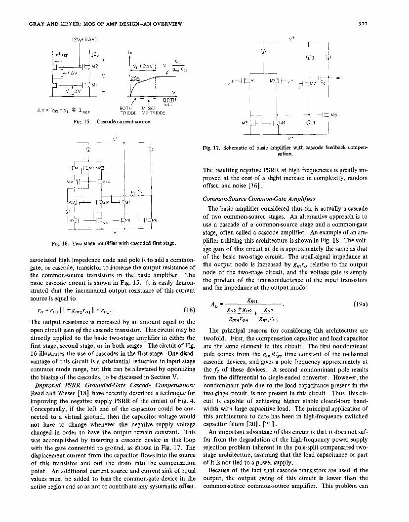
Fig. 15.
,oTH/-& WHTRIODE M2 TRIODE
Cascode current source.
k&A4MA ~ M2A
~7 cc
M3A M4A M?
J
M3 +- r M4M8 + M6
~–
Fig. 16. Two-stage amplifier with cascoded fiist stage.
associated high impedence node and pole is to add a common-
gate, or cascode, transistor to increase the output resistance of
the common-source transistors in the basic amplifier. The
basic cascode circuit is shown in Fig. 15. It is easily demon-
strated that the incremented output resistance of this current
source is equal to
/-0 = ro~ [1 +gm2r01] +ro~. (18)
The output resistance is increased by an amount equal to the
open circuit gain d the cascode transistor. This circuit maybe
directly applied to the basic two-stage amplifier in either the
first stage, second stage, or in both stages. The circuit of Fig.
16 illustrates the use of cascodes in the first stage. One disad-
vantage of this circuit is a substantial reduction in input stage
common mode range, but this can be alleviated by optimizing
the biasing of the cascodes, to be discussed in Section V.
Improved PSRR Grounded-Gate Cascode Compensation:
Read and Wieser [18] have recently described a technique for
improving the negative supply PSRR of the circuit of Fig. 4.
Conceptually, if the left end of the capacitor could be con-
nected to a virtual ground, then the capacitor voltage would
not have to change whenever the negative supply voltage
changed in order to have the output remain constant. This
was accomplished by inserting a cascode device in this loop
with the gate connected to ground, as shown in Fig. 17. The
displacement current from the capacitor flows into the source
of this transistor and out the drain into the compensation
point. An additional current source and current sink of equal
values must be added to bias the common-gate device in the
active region and so as not to contribute any systematic offset.
TT!‘-+T’TV++F”UM=HM6~ ~..~ ~-
Fig. 17. Schematic of basic amplifier with cascode feedback compen-
The resulting negative PSRR at high frequencies is greatly im-
proved at the cost of a slight increase in complexity, random
offset, and noise [16] .
Common-Source Common-Gate Amplifiers
The basic amplifier considered thus far is actually a cascade
of two common-source stages. An alternative approach is to
use a cascade of a common-source stage and a common-gate
stage, often called a cascode amplifier. An example of an am-
plifier utilizing this architecture is shown in Fig. 18. The volt-
age gain of this circuit at dc is approximately the same as thatof the basic two-stage circuit. The small-signal impedance at
the output node is increased by gmro relative to the output
node of the two-stage circuit, and the voltage gain is simply
the product of the transconductance of the input transistors
and the impedance at the output mode:
Au=gm 1
(19a)go2 + &709 + go7 “
gm4r04 gm5r05
The principal reasons for considering this architecture are
twofold. First, the compensation capacitor and load capacitor
are the same element in this circuit. The first nondominant
pole. comes from the gm /Cg~ time constant of the n-channelcascode devices, and gives a pole frequency approximately at
the ft of these devices. A second nondominant pole results
from the differential to single-ended converter. However, the
nondominant pole due to the load capacitance present in the
two-stage circuit, is not present in this circuit. Thus, this cir-
cuit is capable of achieving higher stable closed-loop band-
width with large capacitive load. The principal application of
this architecture to date has been in high-frequency switched
capacitor filters [20], [21 ].
An important advantage of this circuit is that it does not suf-fer from the degradation of the high-frequency power supply
rejection problem inherent in the pole-split compensated two-stage architecture, assuming that the load capacitance or part
of it is not tied to a power supply.
Because of the fact that cascode transistors are used at the
output, the output swing of this circuit is lower than the
common-source common-source amplifier. This problem can

978 IEEE JOURNAL OF SOLID-STATE CIRCUITS, VOL. SC-17, NO. 6, DECEMBER 1982
T“--!?-i-6’A’—“+-...
M5
‘8 F “
J-
l.—
I
r
.;–+ .M1 M2 ~ –v,.
P
%
~
!“
1 IA’’”L—
__:fiB’A’v-
Fig. 18. One-stage amplifier schematic.
be minimized by modifying the bias generator such that the
lower transistors in the cascode current source are biased on
the edge of saturation (i.e., Vgd = VT). This results in an avail-
able output voltage swing within 2(Vg~ - VT) of each supply,
or perhaps 0.4 to 0.8 V in voiceband filters. MOS transistors
actually display a rather indistinct transition from triode to
saturation as the drain depletion region forms, and as a result,
the bias point must actually be chosen so as to bias the lower
transistor a few hundred millivolts into saturation if the pre-
dicted value of incremental output resistance is to be obtained.
A second disadvantage of this circuit is that more devices
contribute to the input-referred voltage and input offset volt-
age. Assuming that transistors Lf5-lf8 are biased at the same
current as the input devices, the input-referred flicker noise
can be shown to be
“q=%[’+%wwl% (19b)
In this case, the current sources M9 and Ml O contribute an
additional term not present in (16). However, as in the case of
the common-source common-source amplifier, the equivalent
input noise can be made almost equivalent to the noise of the
input transistors alone by choosing the channel lengths of the
input transistors to be short compared to those of M5, M6,
M9, and Ml O. The same considerations apply for the thermal
noise.
Class AB Amplifiers. Dynamic Amplifiers. andDynamic Biasing
Many, if not all, MOS analog circuits commercially produced
utilize class AB circuitry in some form. Here the term class
AB is taken to mean a circuit which can source and sink cur-
rent from a load which is larger than the dc quiescent current
flowing in the circuit. The most widespread application is in
output buffers, but if an important objective is the minimiza-
tion of chip power, then the philosophy of using class AB op-
eration can be extended to the internal amplifiers. The moti-
vation for doing so is that one of the factors that dictates the
value of the quiescent current with an MOS amplifier is the
v+
I 1 I
I IT I L
l% I L“9
Fig. 19. Example circuit illustrating class.0 second stage.
value of current required to charge the load and/or the com-
pensation capacitance in the required time. However, it is rela-
tively rare that the operational amplifier outputs actually have
to change the maximum amount in one clock cycle. Large
power savings can be effected if only that current is drawn
which is required to charge the capacitance on that particular
cycle. An example of an amplifier utilizing a class A first
stage and a class AB second stage is shown in Fig. 19 [22] . In
a conventional circuit, the gate of M2 would be connected to a
level-shifted version of the stage input voltage. Thus, when the
first stage output swings positive, reducing the current in Ml,
the current in M2 increases above its quiescent dc value. An
example of a single-stage amplifier that operates on this prin-
ciple is shown in Fig. 20 [23] . This particular circuit can be
used in the inverting mode only. With the input grounded, the
quiescent current in the input transistors is determined by the
bias voltages shown. Upon the application of a voltage to the
input, the current in one side of the input stage increases
monotonically with the applied voltage until the power supply
is reached, while the other side of the input stage turns off.
The amount of current available at the output is much larger
than the quiescent current, and the circuit, as a result, does
not follow the relationship of (12). In fact, the circuit does
not display slew rate limiting in the usual sense. Another as-
pect of this circuit is the fact that the small-signal voltage gain
in the quiescent mode can be quite high because of the low
current level, and the fact that the voltage gain falls off during
transients because of the high current levels is of little conse-
quence. Similar circuits have been used extensively in bipolartechnology [24] .
Degrauwe et al. [25] have recently described a novel ap-
proach to the same objective. A conventional class A amplifier
configuration is used, but an auxiliary circuit is used to detect
the presence of large differential signals at the input. The bias
current in the class A circuitry is then increased when such sig-
nals are present. Experimental versions of such amplifiers have
yielded quiescent power dissipation of less than 10 vW.
A second class of amplifiers has been explored by several
authors, beginning with Copeland [26] , in which the quiescent
current in the absence of signals is allowed to decay to zero.
Such amplifiers are fully dynamic in the sense that no dc paths

GRAY AND MEYER : MOS OP AMP DESIGN–AN OVERVIEW 979
IN
nD’-Fig. 20. Examples of a single-stage class ,4~ op amp.
exist for current to flow from the supply. While very low val-
ues of power dissipation can be obtained, difficult problems of
settling time and power supply rejection remain to be solved
with these amplifiers.
Hostica [27] has described a third approach to micropower
amplifier design for switched capacitor applications which uti-
lizes a time-varying periodic bias current which is synchro-
nous with the master clock in the filter. In contrast to the ap-
proaches described above, the power supply current is inde-
pendent of signal amplitude, and is made large during the early
part of the clock period for fast slewing and small during the
later portion for high gain and power savings. The bias current
waveform is generated by discharging a capacitor into the in-
put of a current mirror. While this technique, in principle,
dissipates more power than the other approaches under low
signal conditions, it can be implemented with relatively simple
circuitry, and it has demonstrated good experimental results
for both one-stage and two-stage amplifiers [28] .
V. DIFFERENTIAL OUTPUT AMPLIFIERS
As has been mentioned, power supply rejection is an impor-
tant performance parameter for amplifiers to be used in comp-
lex analog/digital systems. In addition, one inevitable result
of technology scaling is a reduction in power supply voltage
with an accompanying reduction in internal signal swings and
dynamic range. These two considerations make use of fully
differential signal paths throughout the analog portions of
the system attractive for some systems [29] , [30] . The in-
herently differential nature of the circuit tends to give very
high PSRR since the supply variations appear as a common
mode signal. Also, the effective output swing is doubled,
while the magnitude of the input-referred operational ampli-
fier noise remains the same, giving a 6 dB improvement in op-
erational amplifier noise-limited dynamic range.
A typical implementation of a differential switched capaci-
tor integrator is shown in Fig. 21. The operational amplifier is
required to produce two analog outputs which are symmetric
about ground, in contrast to the single-ended case where only
one is produced. An equivalent circuit for a differential op
-Vo+~o-
Fig. 21. Differential switched capacitor integrator.
p,,1 -.
,,,
-’.
$ “ --J -,
-. ++,,.‘R
-.-.
-,>,/
R /
1= ‘/’
\
,. -“
+ ~. .,
‘.>.,’
.-.
1 /’I ..’,,. ‘
STANDARDSIPJ6LE-ENDEDOP AMPS
Fig. 22. Equivalent circuit for a differential output operationalamplitler.
n.$’BIAS
M8 M7
{ Ml M2 h
M3
L
L,
MIO —
cMFB
~-
;
M4BIAS
BIA s
M9
Fig. 23. Example of a differential output amplifier. The block labeledClfFB serves to keep the common-mode output voltage near ground.
amp is shown in Fig. 22. An example of a CMOS differential
output operational amplifier is shown in Fig. 23.
An important problem in such amplifiers is the design of afeedback loop to force the common mode output voltage to
be ground or some other internal reference potential. Thisfeedback path can be implemented with transistors in a con-
tinuous-time circuit or can be implemented with switched
capacitor circuitry. The continuous approach is potentially
simpler, but presents a difficult design problem in making the
common-mode output voltage independent of thp differential
mode signal voltage [21 ] , [29]. Switched capacitor circuitry
can make use of the linearity of MOS capacitors to achieve this
goal [30]. The choice between the two techniques depends
on the sensitivity of the particular application to variations in
common-mode voltage.

IEEE JOURNAL OF SOLID-STATE CIRCUITS, VOL. SC-17, NO. 6, DECEMBER 1982
~+T
Fig. 24. Small-signal differential half circuit for the amplifier in Fig. 23.
Another important advantage of differential output ampli-
fiers is that the differential single-ended converter with its
associated nondominant poles is eliminated. The small-signal
equivalent circuit for the circuit in Fig. 22, for example, is a
simple common-source common-gate cascade, as shown in Fig.
24. This circuit has only one nondominant pole, at theft of
the common-gate device. Thus the configuration is particu-
larly well suited to the implementation of high-frequency
switched capacitor filters. A configuration of this type has
been used in recently reported work yielding high-Q switched
capacitor filters clocked at 4 MHz with center frequencies of
250 kHz in a 4 pm silicon gate CMOS technology [21 ] .
VI. NMOS OPERATIONAL AMPLIFIERS
The design of an operational amplifier of a given perfor-
mance level in NMOS depletion load technology is a much
more difficult task than in CMOS technology. The absence of
a complementary device makes the implementation of level
shifters which track supply voltage variations much more com-
plex. The level of body effect found in most depletion load
devices makes the realization of large gains per stage difficult.
Assuming that the basic architecture is similar to that illus-
trated in Fig. 2(c), the small-signal properties, voltage gain,
transient response and slew rate, input noise, and power sup-
ply rejection considerations are basically similar to the two-
stage CMOS amplifier. The key additional considerations are
the shunting effects of the incremental output conductance of
the depletion load current sources and the impedance and
power supply variation of the floating level-shifting voltage
sources and the resulting degradation of power supply rejec-
tion ratio. Nonetheless, creative circuit design has resulted in
NMOS amplifiers which nearly match CMOS amplifiers in
most performance aspects, albeit at the cost of somewhat
more complexity, die area, and power dissipation. Circuittechniques used to achieve this include replica biasing for
tracking level shifters [9] , [17] , positive feedback for high
voltage gain [31 ] , [30] , differential configurations for power
supply rejection [29 ], [30], and others.
While there will no doubt always be a need for NMOS ampli-
fiers for some applications, the emergence of CMOS as a key
VLSI digital technology has resulted in the widespread adop-
tion of CMOS for new mixed analog-digital designs.
VII. OUTPUT BUFFERS
In amplifier applications involving either a large capacitive or
resistive load, an output stage must be added to the basic am-
plifier to prevent the load from degrading the voltage gain or
closed-loop stability. This situation most often arises when
signals must be supplied off the chip to an external environ-
ment. The key requirements on such stages is that they be suf-
ficiently broad band with heavy capacitive loading such that
they do not degrade the loop stability of the operational am-
plifier, and such that the output is able to supply a large
enough voltage swing to the load with the maximum load con-
ductance. While class A source follower or emitter follower
circuits can be used in some applications, quiescent power dis-
sipation considerations usually dictate a class AB implementa-
tion of the circuit. This discussion is limited to class Al? out-
put buffers.
In bipolar operational amplifier design, the complementary
emitter follower class AB configuration is used in the vast
majority of cases. In contrast, class All CMOS output stage
implementations tend to vary widely, depending on the spe-
cific devices available in the particular technology used. The
CMOS complementary source follower class Al? output buffer
stage shown in Fig. 25 is a direct analog of its bipolar counter-
part. The primary drawback of this circuit is that the output
voltage swing is limited by the gate-source voltage of the out-
put transistors. This occurs because the transistors used for
logic functions on the chip have thresholds in the 0.5-1 V
range, so that the amount of swing lost due to threshold voh-
age plus the (Vg~ - VT) drop is too large for many applica-
tions. However, many technologies have an extra device type
with very low threshold voltage, and in this case, this low
threshold device can be used for one of the two output transis-
tors. It is rare that both p-channel and n-channel low thresh-
old devices are available in the same technology.
In many CMOS technologies, a bipolar transistor follower is
available and can be used in place of one of the output fol-
lowers. This provides very low output resistance and good
output swing. In processes with light substrate doping, poten-
tial latchup problems can make the use of such devices in off-
chip driver stages impractical because of the fact that the col-
lector current of the transistor flows in the substrate and can
cause voltage drops which cause a junction to be forward
biased. An example of the use of a bipolar device in an MOS
output stage together with a low threshold device is illustrated
in Fig. 26.
A third alternative is the use of quasi-complementary con-
figurations in which a common-source transistor together with
an error amplifier is used in place of one or both of the fol-
lower devices. This circuit is shown conceptually in Fig. 27.The combination of the error amplifier and the common-
source device mimics the behavior of a follower with high dc
transconductance. Such quasi-complementary circuits provide
excellent dc performance with voltage swings approaching the
supply rails, but since the amplifier must be broad band to pre-
vent crossover distortion problems, they present difficult prob-
lems in compensation of the local feedback loop in the pres-
ence of large capacitive loads. Proper control of the quiescent
current is also a key design constraint.
Low threshold devices, bipolar devices, and quasi-comple-
mentary devices can be used in any combination, depending
on what devices are available in the particular technology

GRAY AND MEYER: MOSOP AMP DESIGN–AN OVERVIEW 981
Fig. 25.
/
Fig. 26.
Fig. 27’.
Complementary source follower CMOS output stage basedonthe traditional bipolar implementation.
v+
Example ofa CMOS output stage using abipolar emitter fol-lower and a low-threshold p-channel source follower.
I
~1
—
‘$”V’1
>
I“-
Example of a complementary classll output stage using corn-pound devices with imbedded common-source output transistors.
being used. Whereas inthebipolar case thevast majority of
output stage applications can be satisfied using the traditional
complementary class 13 emitter follower stage, no single circuit
approach has yet emerged as the standard for CMOS output
stages.
VIII. SUMMARY AND CONCLUSIONS
In this paper, we have attempted to summarize the various
techniques and architectures which have been applied in the
design of MOS operational amplifiers in the past several years.
An important question is the extent to which these amplifier
designs can be scaled as minimum feature sizes continue to de-
crease. As pointed out in a recent study [32] , dc parameters
such as voltage gain are generally unaffected for constant-field
scaling, although they are degraded for quasi-constant voltage
or constant voltage scaling. Perhaps the most difficult prob-
lem results from the fact that the effective dynamic range ofthe amplifier falls in scaled technologies. This occurs funda-
mentally because of the fact that analog signal swings fall with
reductions in power supply voltage. Input-referred thermal
noise remains constant because of the fact that the device
transconductance remains constant under constant-field scal-
ing. The input-referred 1/f noise increases, but this does not
appear to be a fundamental limitation on system dynamic
range because the signal can always be translated to a higher
portion of the spectrum using techniques like chopper stabili-
zation [29] . Also, newer technologies have demonstrated con-
tinuing reductions in 1/f noise as a result of better process
control.
‘In sampled data analog amplifiers, filters and data convert-
ers, the primary limitation on dynamic range, assuming that
1/f noise has been removed, is the kT/C noise contributed by
the analog switches making up the filter. The kT/C limited
dynamic range also falls as the technology is scaled, and since
for practical clock rates and capacitor sizes this noise source is
dominant over op amp thermal noise, there appears to be no
barrier to constant-field scaling of operational amplifiers for
this application, assuming that 1/f noise is removed by circuit
or technological means. Thus, the adaptation of the circuit ap-
proaches described in this paper to lower supply voltages and
scaled devices, and the removal of 1/f noise from the signal
path in such circuits, are important objectives in future work.
[1]
[2]
[3]
[4]
[5]
[6]
[7]
[8]
[9]
[10]
[11]
REFERENCES
D, A. Hodges, P. R. Gray, and R. W. Broderson, “Potential of
MOS technologies for analog integrated circuits: IEEE J. Solid-State Circuits, pp. 285-293, June 1978.J. E. Solomon, “The monolithic Qp amp, A tutorial studyyIEEE J. Solid-State Circuits, vol. SC-9, pp. 314-332, Dec. 1974.Y. P. Tsividis, “Design considerations in single-channel MOS ana-
log circuits-A tutorial;’ IEEE J. Solid-State Circuits, pp. 383-
391, June 1978.
P. R. Gray, “Basic MOS operational amplifier design-An over-view; in Analog MOS Integrated Circuits. New York: IEEE
Press, 1980, pp. 28-49.
R. W. Broderson, P. R. Gray, and D. A. Hodges, “MOS switched
capacitor fiiters~ Proc. IEEE, pp. 61-75, Jan, 1979.
0. H. Shade, Jr., “BiMOS micropower integrated circuits, IEEEJ. Solid-State CYrcuits, vol. SC-13, pp. 791-798, Dec. 1978. See
also O. H. Schade, Jr. and E. J. Kramer, “A low-voltage BiMOS OPamp,” IEEE J. Solid-State Circuits, vol. SC-16, pp. 661-668,Dec. 1981.
Y. P. Tsividis and P. R. Gray, “An integrated NMOS operational
amplifier with internrd compensation,” IEEE J. Solid-state Cir.cuits, vol. SC-11, pp. 748-753, Dec. 1976.P. R. Gray and R. G. Meyer, Analysis and Design of Analog Inte-grated Circuits. New Yor~: Wiley, 1977.D. Senderowicz, D. A. Hodges, and P. R. Gray, “A high-perfor-
mance NMOS operational amplifier’ IEEE J. Solid-State Cir-cuits, vol. SC-13, pp. 760-768, Dec. 1978.
W. C. Black and D. J. Allstott, “Low power CMOS channel fil-ter: IEEE J. Solid-State Circuits, vol. SC-15, pp. 929-938, Dec.
1980.
J. C. Bertails, “Low frequency noise considerations for MOS am-
982
[12]
[13]
[14]
[15]
[16][17]
[18][19]
[20]
[21]
[22]
[23]
[24]
[25]
[26]
[27]
[28]
[29]
[30]
IEEE JOURNAL OF SOLID-STATE CIRCUITS, VOL. SC-17, NO. 6, DECEMBER 1982
plifier design:’ IEEE J. Solid-State Circuits, vol. SC-14, pp. 773-
776, Aug. 1979.
M. B. Das and J. M. Moore, “Measurements and interpretation oflow-frequency noise in FET’sj” IEEE Trans. Electron Devices,vol. ED-21, Apr. 1974.
N. R. Mantena and R. C. Lucas, “Experimental study of flickernoise in MIS transistors: Electron. Lett., vol. 5, pp. 697-603,
1969.H. Mikoshiba, “l/f noise in n-channel silicon gate MOS transis-
tor” IEEE Trans. Electron Devices, vol. ED-29, June 1962.E. Vittoz and J. Fellrath, “CMOS inte~ated circuits based onweak inversion operation,” IEEE J. Solid-State Circuits, vol. SC-
12, pp. 214-231, June 1977.B. Ahuja, Intel Corporation, private communication.H. Ohara, W. M. Baxter, C. F. Rahim, and J. L. McCreary, “Aprecision low power PCM channel filter with on-chip power sup-ply regnlation~’ IEEE J. Solid-State Circuits, vol. SC-15, pp.
1005-1013, Dec. 1980.R. Read, private communication.P. R. Gray and R. G. Meyer, “Recent advances in monolithic op-
erational amplifier design,” IEEE Trans. Circuits Syst., pp. 317-
327, May 1974.P. R. Gray, R. W. Broderson, D.A. Hodges, T. C. Choi, R. Kane-
shiro, and K. C. Hsieh, “Some practical aspects of switched ca-pacitor filter design: in Dig. Tech. Papers, 1981 Int. Symp. Cir-cuits Syst.T. Choi, R. Kaneshiro, R. W, Broderson, and P. R. Gray, “Highfrequency CMOS switched capacitor filters for communications
applications, “ in Dig. Tech. Papers, 1983 Int. Solid-State CircuitsCon~Y. A. Haque, R. Gregortan, D. Blasco, R. Mao, and W. Nicholson,“A two-chip PCM codec with filters,” IEEE J. Solid-State Cir-cuits, vol. SC-24, pp. 961-969, Dec. 1979.W. Black, personal communication.P. C. Davis and V. Saari, “A high slew rate monolithic op ampusing compatible complementary PNPs,” in Dig. Tech. Papers,IEEE Int. Solid-State Circuits Con$, Philadelphia, PA, Feb. 1974.M. G. Degrauwe, J. Rijmenants, E. A. Vittoz, and H. J. De Man,
“Adaptive biasing CMOS amplifiers;’ IEEE J. Solid-State Cir-cuits, vol. SC-17, pp. 522-528, June 1982.M. A. Copeland and J. M. Rabaey, “Dynamic u amplifiers fo~MOS technology,” Electron. Lett., vol. 15, pp. 301-302, May
1979.B. J. Hosticka, “Dynamic CMOS amplifiers;’ IEEE J. Solid-StateCircuits, vol. SC-15, pp. 887-894, Oct. 1980.
B. J. Hosticka, D. Herbst, B. Hoefflinger, U. Kleine, J. Pandel,and R. Schweer, “ReaJ-time programmable low-power SC band-
pass filter,” IEEE J. Solid-State Circuits, vol. SC-G’, pp. 499-
506, June 1982.K. C. Hsieh, P. R. Gray, D. Senderowicz, and D. Messerschmitt,
“A low-noise differential chopper stabilized switched capacitor
filtering technique,” IEEE J. Solid-State Circuits, VOL SC-16,pp. 708-715, Dec. 1981.D. Senderowicz, S. F. Dreyer, J. M. Huggins, C. F. Rahhn, and
C. A. Laber, “Differential NMOS analog building blocks for PCMtelephony,” in Dig. Tech. Papers, 1982 Int. Solid-State CircuitsCorrf, San Francisco, CA, Feb. 1982. Also appears in full lengthform in this issue, pp. 1014-1023.
[31 ] J. Guinea and D. Senderowicz, “High frequency NMOS switchedcapacitor filters using positive feedback techniques,” this issue,
pp. 1029-1038.[32] S. Wong and C. A. T. Salama, “ScaJing of MOS analog circuits for
VLSI applications,” in Dig. Tech. Papers, 1982 Symp. VLSITechnology, Tokyo, Japan, Sept. 1982.
Additional References on MOS Operational Amplifiers
[33]
[34]
[35]
[36]
[37]
[38]
F. H. Muss and R. C. Huntington, “A CMOS monolithic 3; digit
A/D converter, “ in Dig. Tech. Papers, 1976 Int. Solid.State Cir-cuits Con.f, Philadelphia, PA, Feb. 1976, pp. 144-145.
A. G. F. Dingwrdl and B. D. Rosenthal, “Low-power monolithicCOS/MOS dual-slope 1 l-bit AID converters~’ in Dig. Tech. Pa-pers, 1976 Int. Solid-State Circuits Confi, Philadelphia, PA, Feb.1976, pp. 146-147.Y. P. Tsividis and D. Fraser, “A process insensitive NMOS opera-
tional amplifier,” in Dig. Tech. Papers, 1979 Int. Solid-State Cir-cuits Conj!, Philadelphia, PA, Feb. 1979, pp. 188-189.
S. Kelley and D. Ulmer, “A single-chip PCM codec,” IEEE J.Solid-State Circuits, vol. SC-14, pp. 54-58, Feb. 1979.
B. J. White, G. M. Jacobs, and G. Landsburg, “Monolithic dual
tone multifrequency receiver,” IEEE J. Solid-State Circuits, vol.SC-14, pp. 991-997, Dec. 1979.L A. Young, “A high performance all-enhancement NMOS opera-tional amplifier,” IEEE J. Solid-State Circuits, vol. SC-14, pp.
1070-1076, Dec. 1979.
Paul R. Gray (S’56-M’69-SM76 -F’8 1), for a photograph and biogra-phy, see p. 419 of the April 1982 issue of this JOURNAL.
Robert G. Meyer (S’64-M’68-SM’7 4-F’81) wasborn in Melbourne, Australia, on July 21, 1942.
He received the B. E., M.Eng.Sci., and Ph.D. de-grees in electrical engineering from the Univer-
sit y of Melbourne, Melbourne, Austr@ia, in
1963, 1965, and 1968, respectively.In 1968 he was employed as an Assistant Lec-
turer in Electrical Engineering at the Universityof Melbourne. Since September 1968, he hasbeen employed in the Department of Electrical
Engineering and Computer Sciences, Universityof California, Berkeley, where he is now a Professor. His current re-
search interests are in integrated circuit design and device fabrication.He has been a consultant to Hewlett-Packard, IBM, Exar, and Signetics.
He is coauthor of Analysis and Design of Analog Integrated Circuits(Wiley, 1977), and editor of the book Integrated Circuit OperationalAmplzj”iers (IEEE Press, 1978). He is President of the Solid-State Cir-cuits Council of the IEEE and is a former Associate Editor of the IEEEJOURNAL OF SOLID-STATE CIRCUITS and of the IEEE TRANSACTIONS ONCIRCUITS AND SYSTEMS.