(MOS-FET) Metal Oxide Semiconductor Field- Effect Transistors · Note that the PMOS transistor is...
50
(MOS-FET) Metal Oxide Semiconductor Field- Effect Transistors Microelectronic Circuits - Fifth Edition © Sedra/Smith® Prodi S1-SK 2017
Transcript of (MOS-FET) Metal Oxide Semiconductor Field- Effect Transistors · Note that the PMOS transistor is...

(MOS-FET) Metal Oxide Semiconductor Field-
Effect Transistors
Microelectronic Circuits - Fifth Edition © Sedra/Smith®
Prodi S1-SK
2017

Bipolar Junction Transistor Structure
1. 3 Layers
2. Difficult to make, especially in sub micron
Figure 1. Cross-section of an npn BJT.
Why MOSFET ?
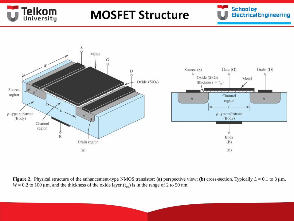
Figure 2. Physical structure of the enhancement-type NMOS transistor: (a) perspective view; (b) cross-section. Typically L = 0.1 to 3 mm,
W = 0.2 to 100 mm, and the thickness of the oxide layer (tox) is in the range of 2 to 50 nm.
MOSFET Structure
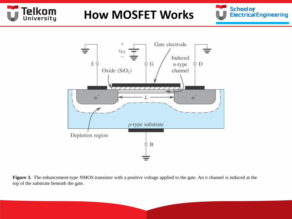
Figure 3. The enhancement-type NMOS transistor with a positive voltage applied to the gate. An n channel is induced at the
top of the substrate beneath the gate.
How MOSFET Works
How MOSFET Works
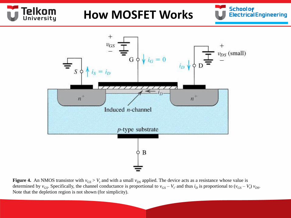
Figure 4. An NMOS transistor with vGS > Vt and with a small vDS applied. The device acts as a resistance whose value is
determined by vGS. Specifically, the channel conductance is proportional to vGS – Vt’ and thus iD is proportional to (vGS – Vt) vDS.
Note that the depletion region is not shown (for simplicity).
How MOSFET Works
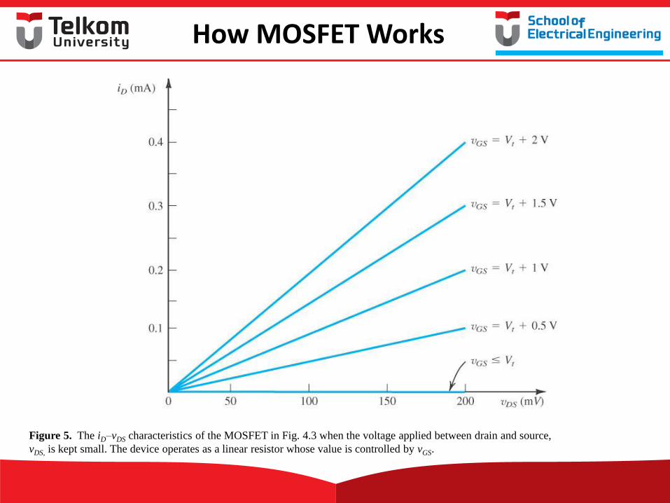
Figure 5. The iD–vDS characteristics of the MOSFET in Fig. 4.3 when the voltage applied between drain and source,
vDS, is kept small. The device operates as a linear resistor whose value is controlled by vGS.
How MOSFET Works
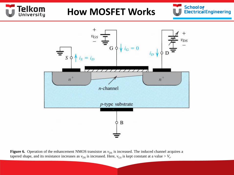
Figure 6. Operation of the enhancement NMOS transistor as vDS is increased. The induced channel acquires a
tapered shape, and its resistance increases as vDS is increased. Here, vGS is kept constant at a value > Vt.
How MOSFET Works
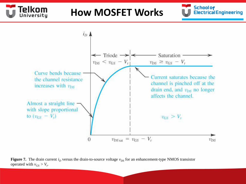
Figure 7. The drain current iD versus the drain-to-source voltage vDS for an enhancement-type NMOS transistor
operated with vGS > Vt.
How MOSFET Works
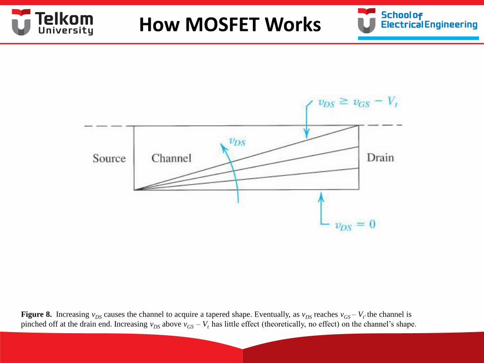
Figure 8. Increasing vDS causes the channel to acquire a tapered shape. Eventually, as vDS reaches vGS – Vt’ the channel is
pinched off at the drain end. Increasing vDS above vGS – Vt has little effect (theoretically, no effect) on the channel’s shape.
How MOSFET Works
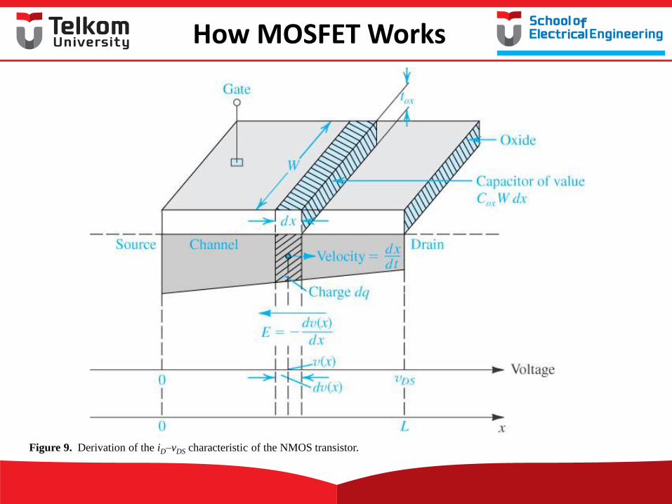
Figure 9. Derivation of the iD–vDS characteristic of the NMOS transistor.
How MOSFET Works

NMOS vs PMOS
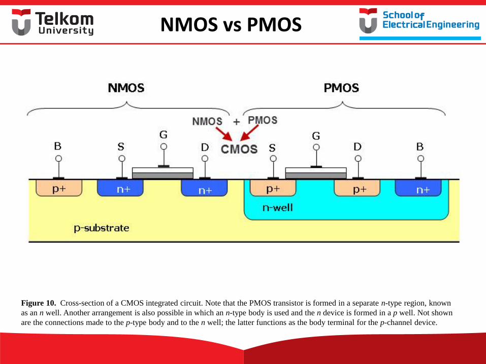
Figure 10. Cross-section of a CMOS integrated circuit. Note that the PMOS transistor is formed in a separate n-type region, known
as an n well. Another arrangement is also possible in which an n-type body is used and the n device is formed in a p well. Not shown
are the connections made to the p-type body and to the n well; the latter functions as the body terminal for the p-channel device.
NMOS vs PMOS
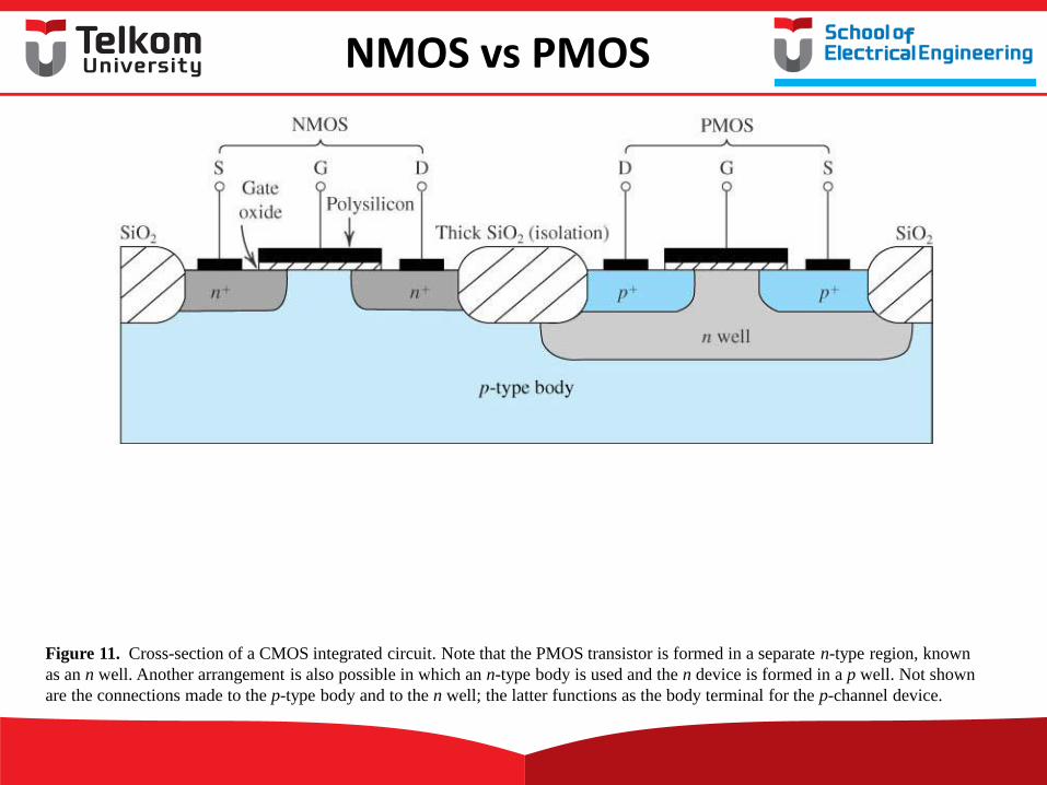
Figure 11. Cross-section of a CMOS integrated circuit. Note that the PMOS transistor is formed in a separate n-type region, known
as an n well. Another arrangement is also possible in which an n-type body is used and the n device is formed in a p well. Not shown
are the connections made to the p-type body and to the n well; the latter functions as the body terminal for the p-channel device.
NMOS vs PMOS
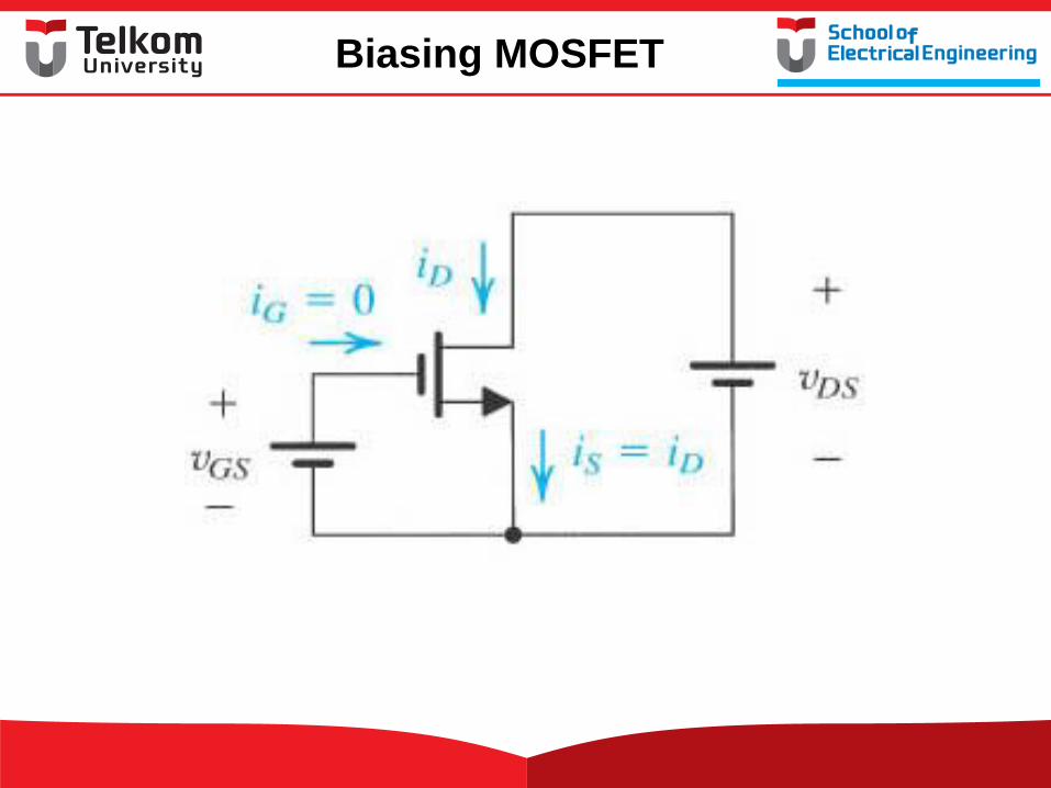
Biasing MOSFET
Biasing MOSFET
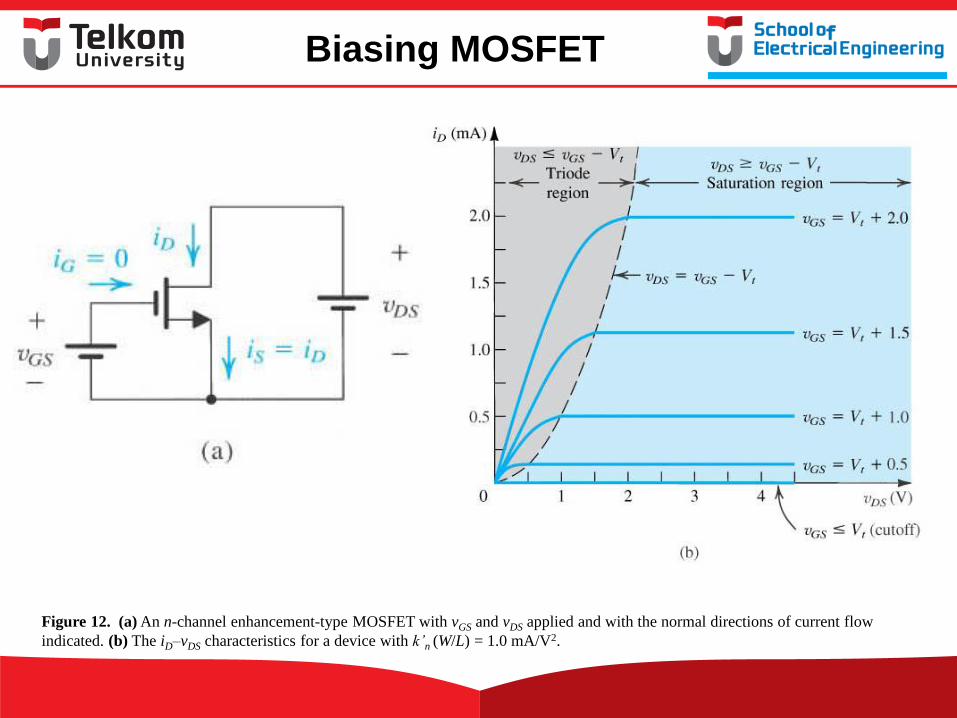
Figure 12. (a) An n-channel enhancement-type MOSFET with vGS and vDS applied and with the normal directions of current flow
indicated. (b) The iD–vDS characteristics for a device with k’n (W/L) = 1.0 mA/V2.
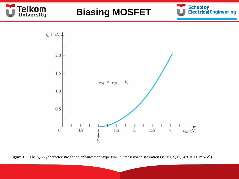
Figure 13. The iD–vGS characteristic for an enhancement-type NMOS transistor in saturation (Vt = 1 V, k’n W/L = 1.0 mA/V2).
Biasing MOSFET
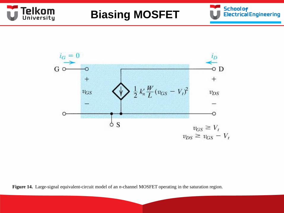
Figure 14. Large-signal equivalent-circuit model of an n-channel MOSFET operating in the saturation region.
Biasing MOSFET
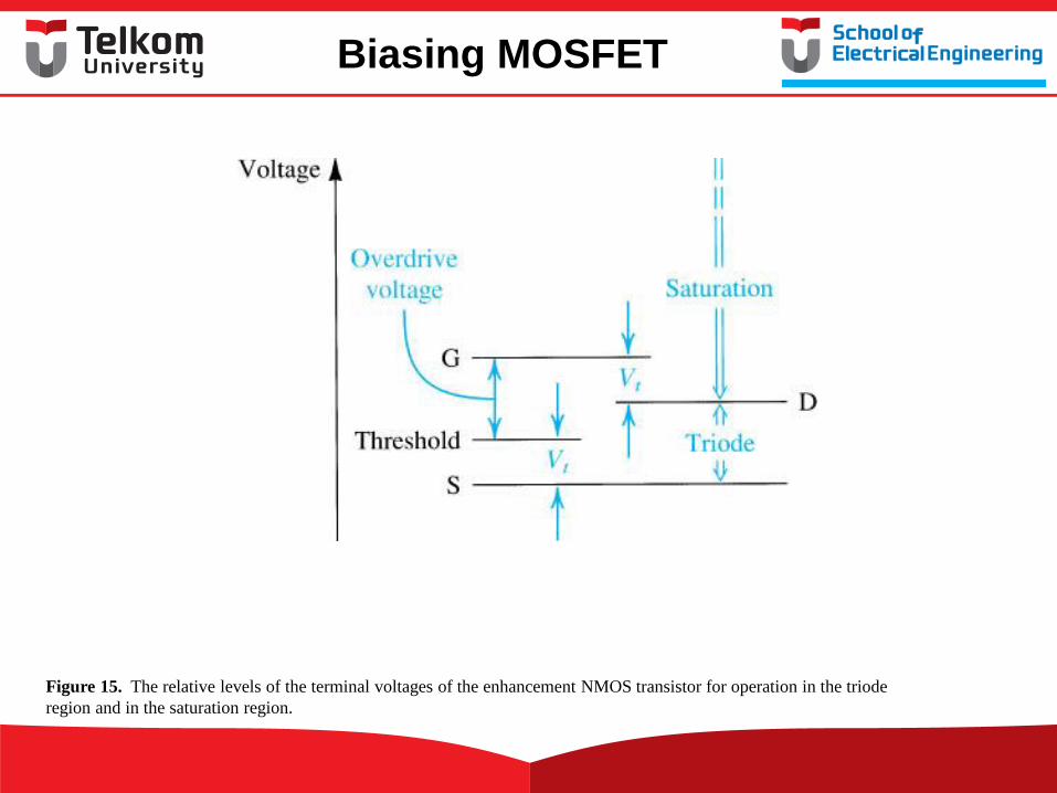
Figure 15. The relative levels of the terminal voltages of the enhancement NMOS transistor for operation in the triode
region and in the saturation region.
Biasing MOSFET
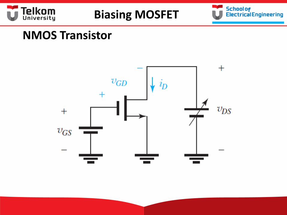
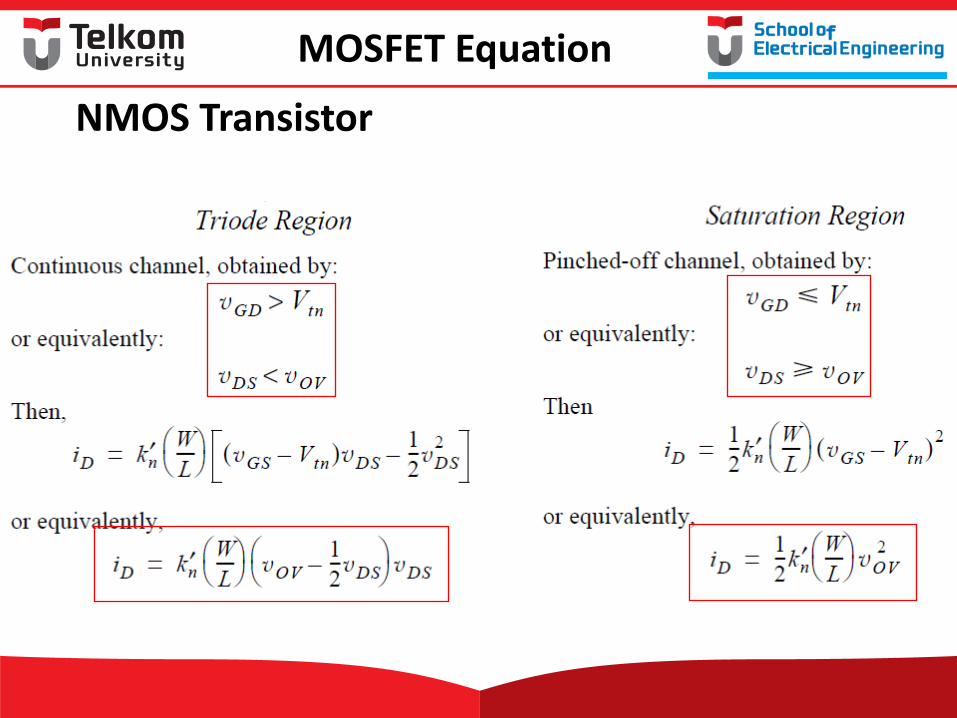
NMOS Transistor
Biasing MOSFET
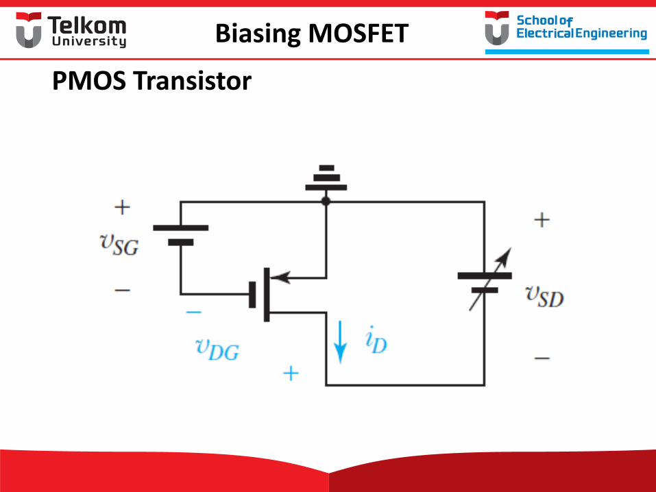
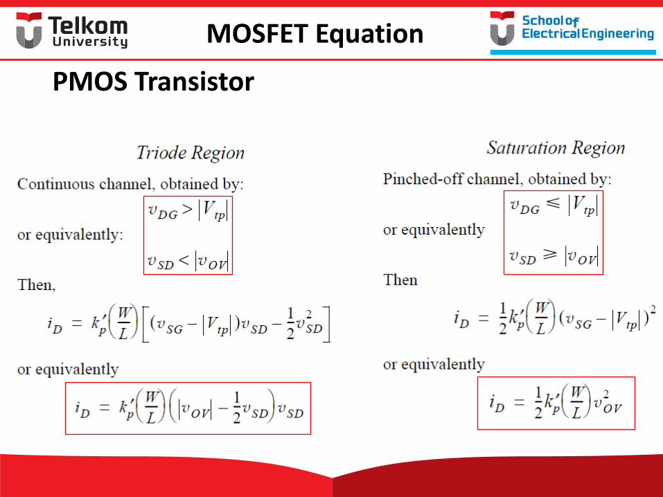
PMOS Transistor
Biasing MOSFET
NMOS Transistor
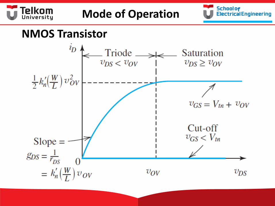
Mode of Operation
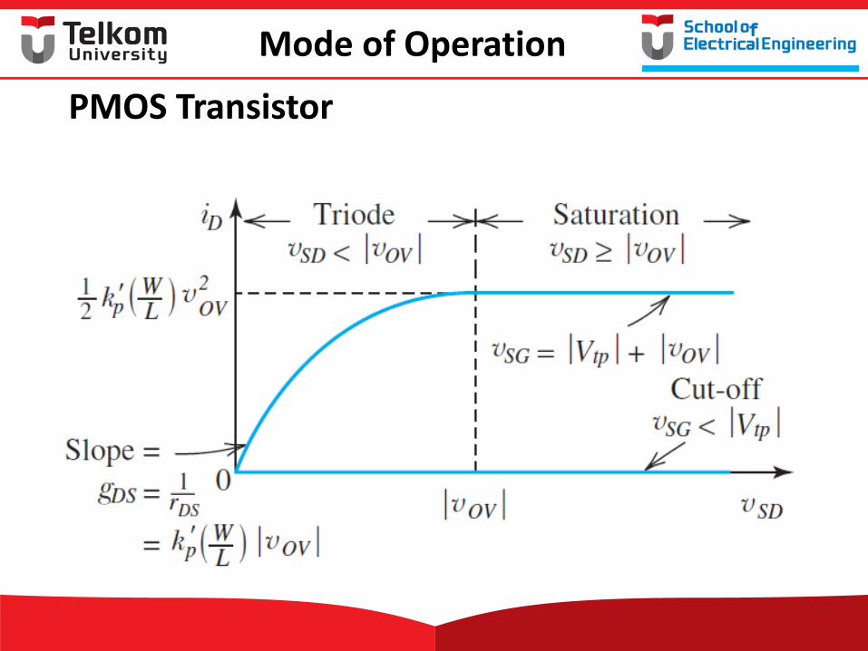
PMOS Transistor
Mode of Operation
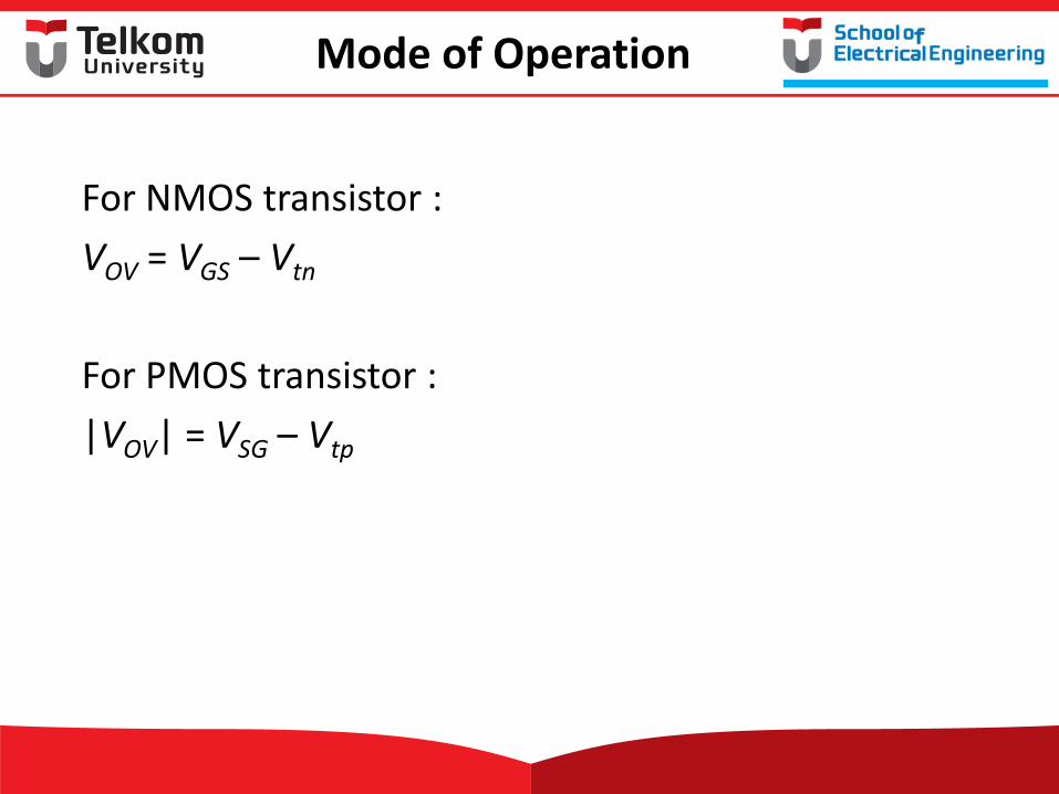
For NMOS transistor :
VOV = VGS – Vtn
For PMOS transistor :
|VOV| = VSG – Vtp
Mode of Operation
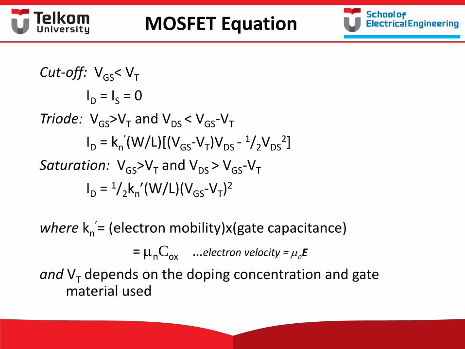
Cut-off: VGS< VT
ID = IS = 0
Triode: VGS>VT and VDS < VGS-VT
ID = kn’(W/L)[(VGS-VT)VDS -
1/2VDS2]
Saturation: VGS>VT and VDS > VGS-VT
ID = 1/2kn’(W/L)(VGS-VT)2
where kn’= (electron mobility)x(gate capacitance)
= mnCox …electron velocity = mnE
and VT depends on the doping concentration and gate material used
MOSFET Equation
NMOS Transistor
MOSFET Equation
PMOS Transistor
MOSFET Equation
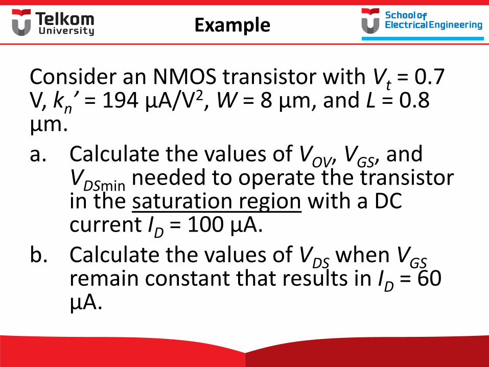
Example
Consider an NMOS transistor with Vt = 0.7 V, kn’ = 194 μA/V2, W = 8 μm, and L = 0.8 μm. a. Calculate the values of VOV, VGS, and
VDSmin needed to operate the transistor in the saturation region with a DC current ID = 100 μA.
b. Calculate the values of VDS when VGS remain constant that results in ID = 60 μA.
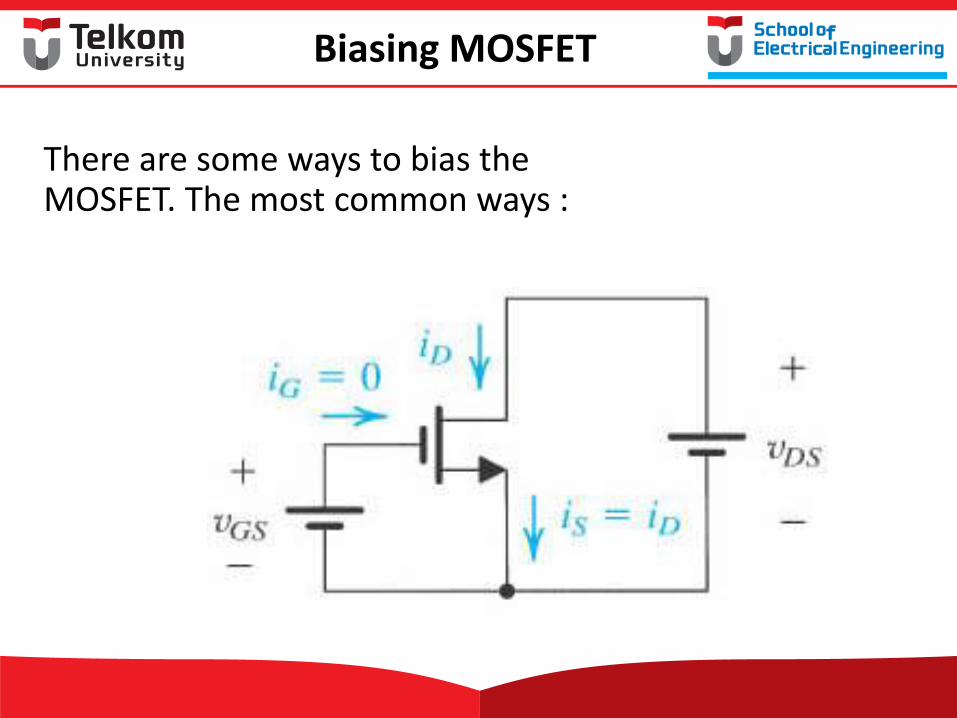
There are some ways to bias the MOSFET. The most common ways :
Biasing MOSFET
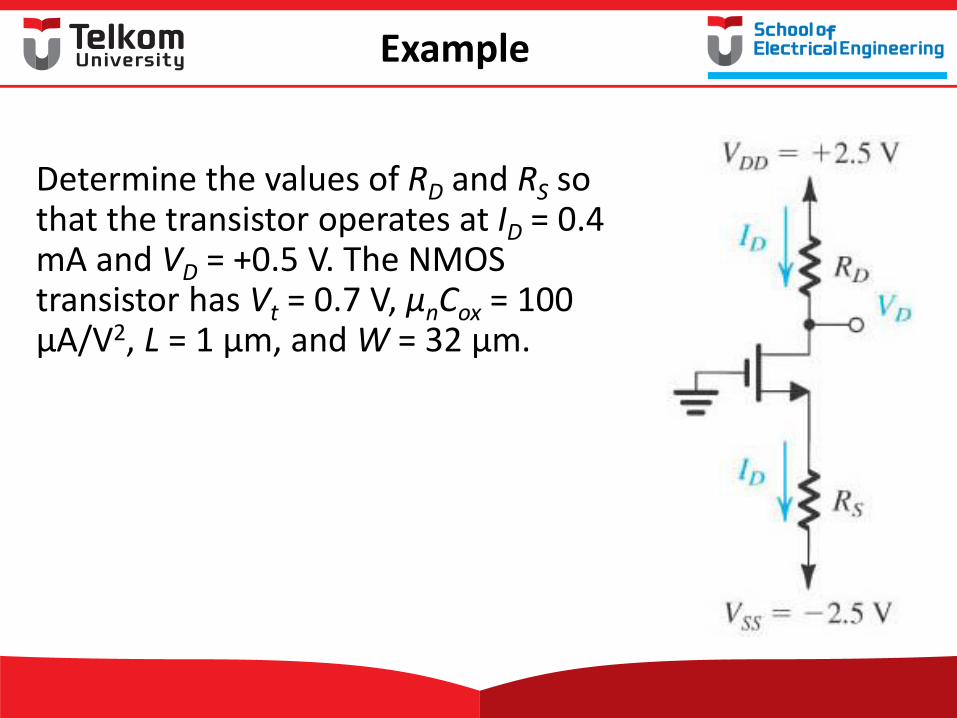
Determine the values of RD and RS so that the transistor operates at ID = 0.4 mA and VD = +0.5 V. The NMOS transistor has Vt = 0.7 V, μnCox = 100 μA/V2, L = 1 μm, and W = 32 μm.
Example
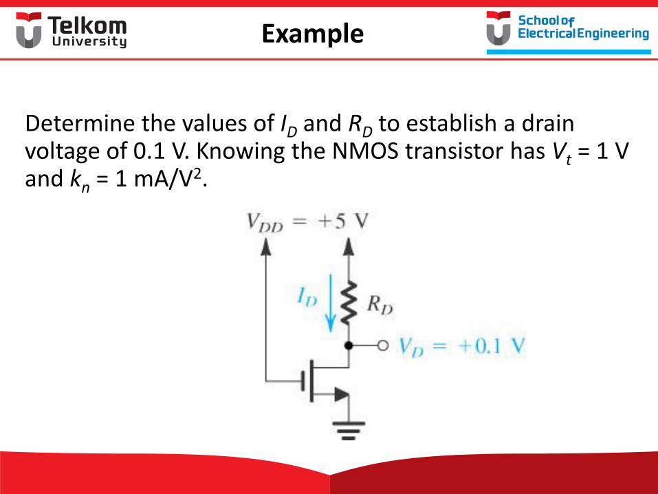
Determine the values of ID and RD to establish a drain voltage of 0.1 V. Knowing the NMOS transistor has Vt = 1 V and kn = 1 mA/V2.
Example
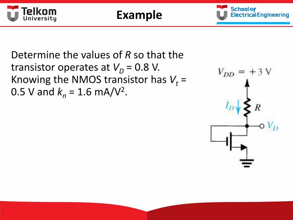
Determine the values of R so that the transistor operates at VD = 0.8 V. Knowing the NMOS transistor has Vt = 0.5 V and kn = 1.6 mA/V2.
Example
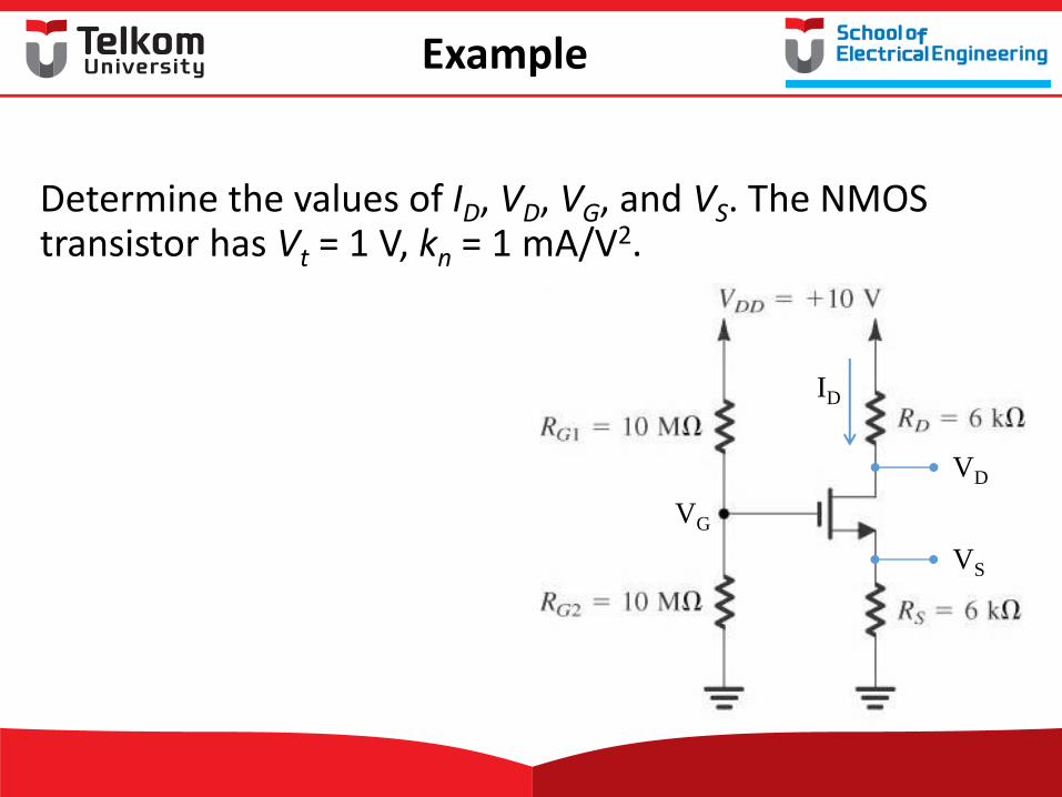
Determine the values of ID, VD, VG, and VS. The NMOS transistor has Vt = 1 V, kn = 1 mA/V2.
VS
VD
VG
ID
Example
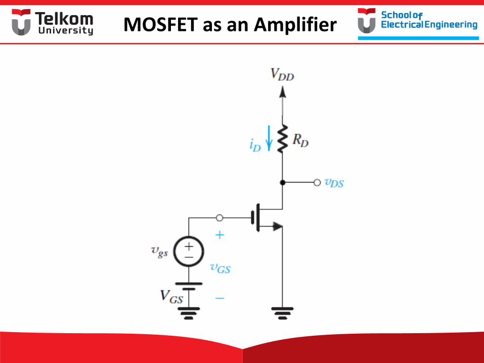
MOSFET as an Amplifier
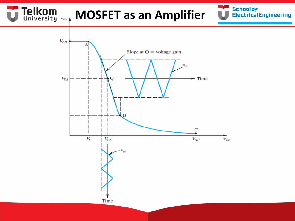
MOSFET as an Amplifier
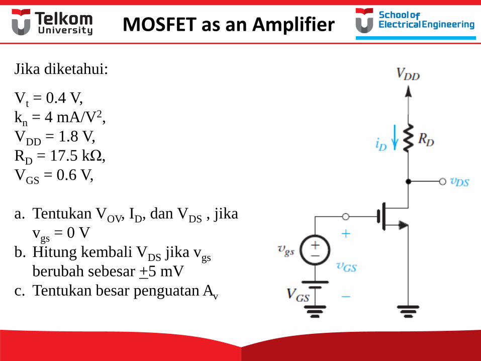
Jika diketahui:
Vt = 0.4 V,
kn = 4 mA/V2,
VDD = 1.8 V,
RD = 17.5 kΩ,
VGS = 0.6 V,
a. Tentukan VOV, ID, dan VDS , jika
vgs = 0 V
b. Hitung kembali VDS jika vgs
berubah sebesar +5 mV
c. Tentukan besar penguatan Av
MOSFET as an Amplifier
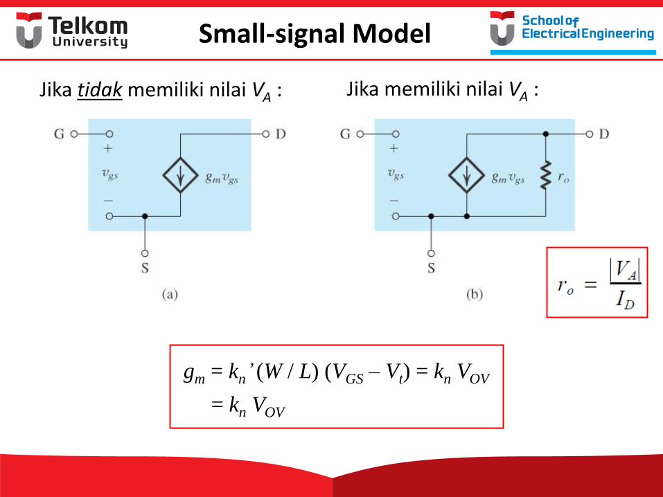
Jika memiliki nilai VA : Jika tidak memiliki nilai VA :
Small-signal Model
gm = kn’ (W / L) (VGS – Vt) = kn VOV
= kn VOV
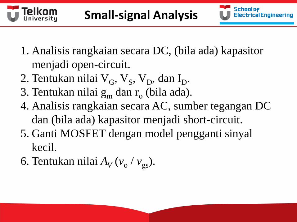
1. Analisis rangkaian secara DC, (bila ada) kapasitor
menjadi open-circuit.
2. Tentukan nilai VG, VS, VD, dan ID.
3. Tentukan nilai gm dan ro (bila ada).
4. Analisis rangkaian secara AC, sumber tegangan DC
dan (bila ada) kapasitor menjadi short-circuit.
5. Ganti MOSFET dengan model pengganti sinyal
kecil.
6. Tentukan nilai AV (vo / vgs).
Small-signal Analysis
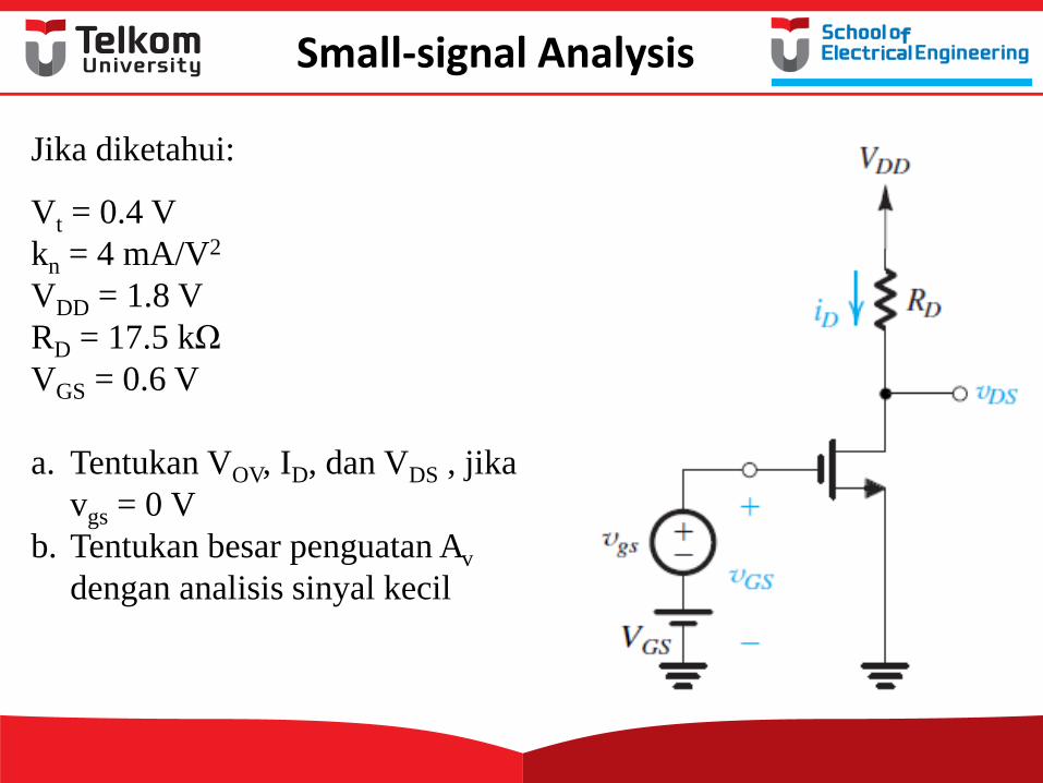
Jika diketahui:
Vt = 0.4 V
kn = 4 mA/V2
VDD = 1.8 V
RD = 17.5 kΩ
VGS = 0.6 V
a. Tentukan VOV, ID, dan VDS , jika
vgs = 0 V
b. Tentukan besar penguatan Av
dengan analisis sinyal kecil
Small-signal Analysis
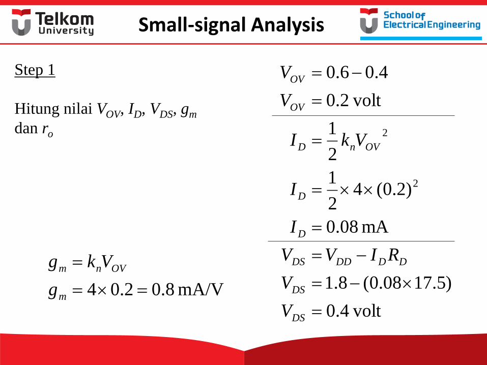
Step 1
Hitung nilai VOV, ID, VDS, gm
dan ro
volt4.0
)5.1708.0(8.1
mA 08.0
)2.0(42
1
2
1
volt2.0
4.06.0
2
2
DS
DS
DDDDDS
D
D
OVnD
OV
OV
V
V
RIVV
I
I
VkI
V
V
mA/V 8.02.04
m
OVnm
g
Vkg
Small-signal Analysis
Step 2
Hilangkan sumber DC
(jadikan short circuit)
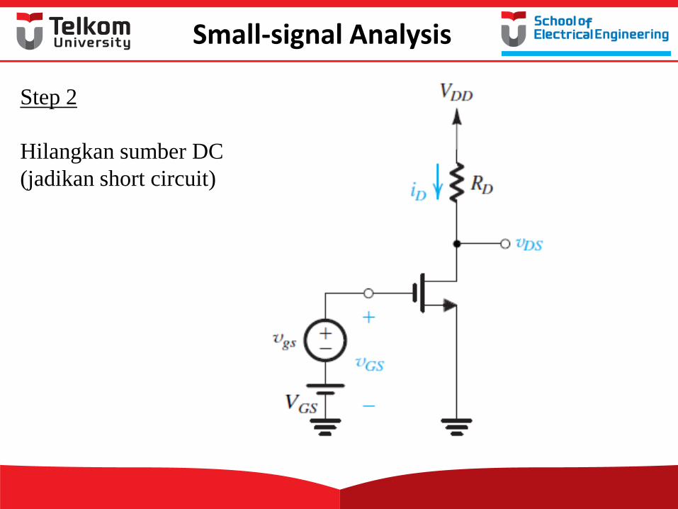
Small-signal Analysis
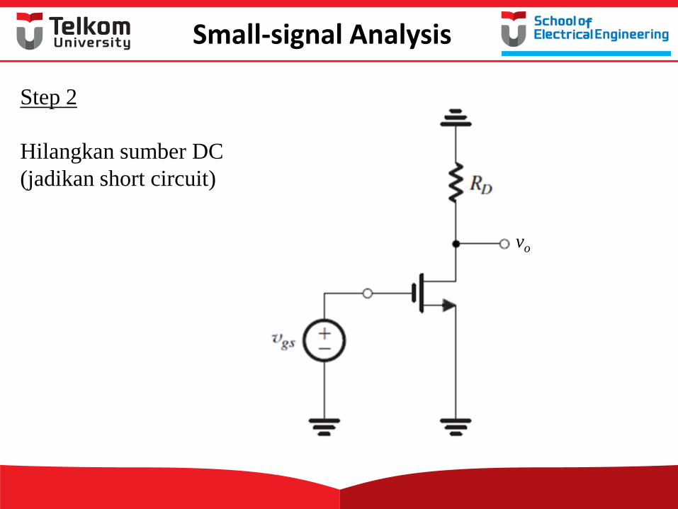
Step 2
Hilangkan sumber DC
(jadikan short circuit)
vo
Small-signal Analysis
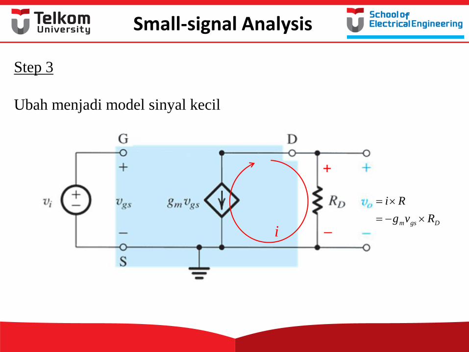
Step 3
Ubah menjadi model sinyal kecil
i Dgsm Rvg
Ri
+
–
Small-signal Analysis
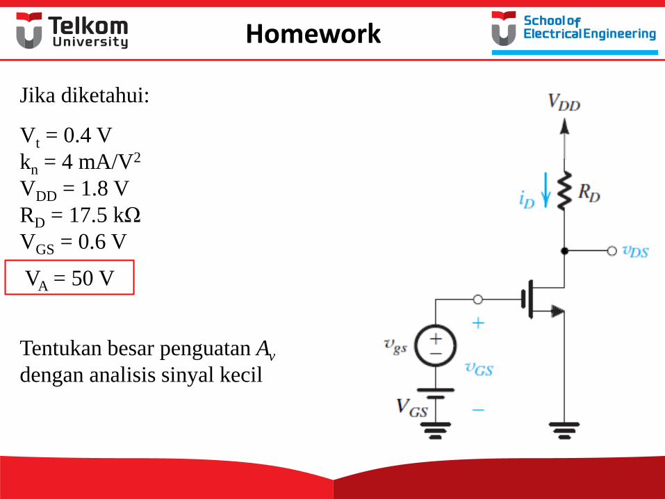
Homework
Jika diketahui:
Vt = 0.4 V
kn = 4 mA/V2
VDD = 1.8 V
RD = 17.5 kΩ
VGS = 0.6 V
Tentukan besar penguatan Av
dengan analisis sinyal kecil
VA = 50 V
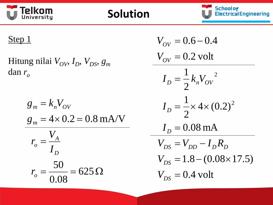
Step 1
Hitung nilai VOV, ID, VDS, gm
dan ro
volt4.0
)5.1708.0(8.1
mA 08.0
)2.0(42
1
2
1
volt2.0
4.06.0
2
2
DS
DS
DDDDDS
D
D
OVnD
OV
OV
V
V
RIVV
I
I
VkI
V
V
62508.0
50
mA/V 8.02.04
o
D
Ao
m
OVnm
r
I
Vr
g
Vkg
Solution
Step 2
Hilangkan sumber DC
(jadikan short circuit)
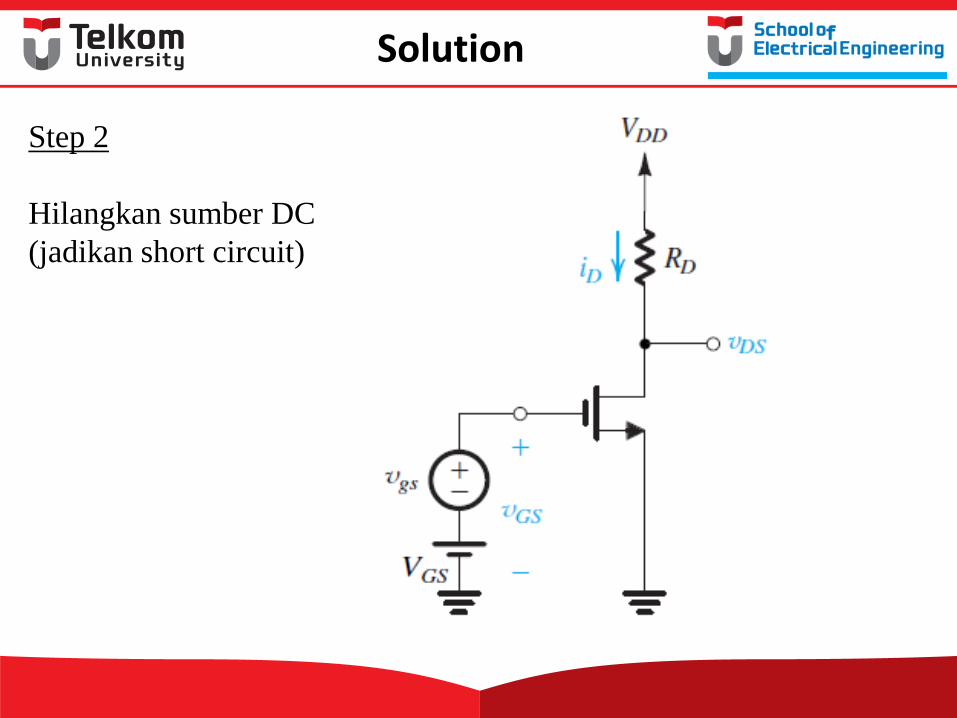
Solution
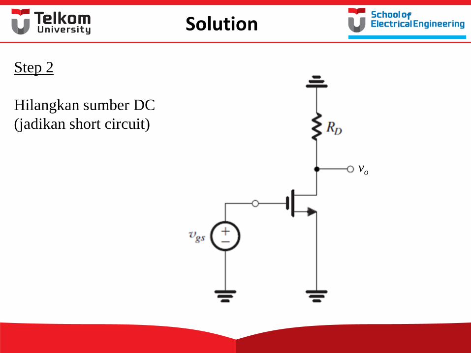
Step 2
Hilangkan sumber DC
(jadikan short circuit)
vo
Solution
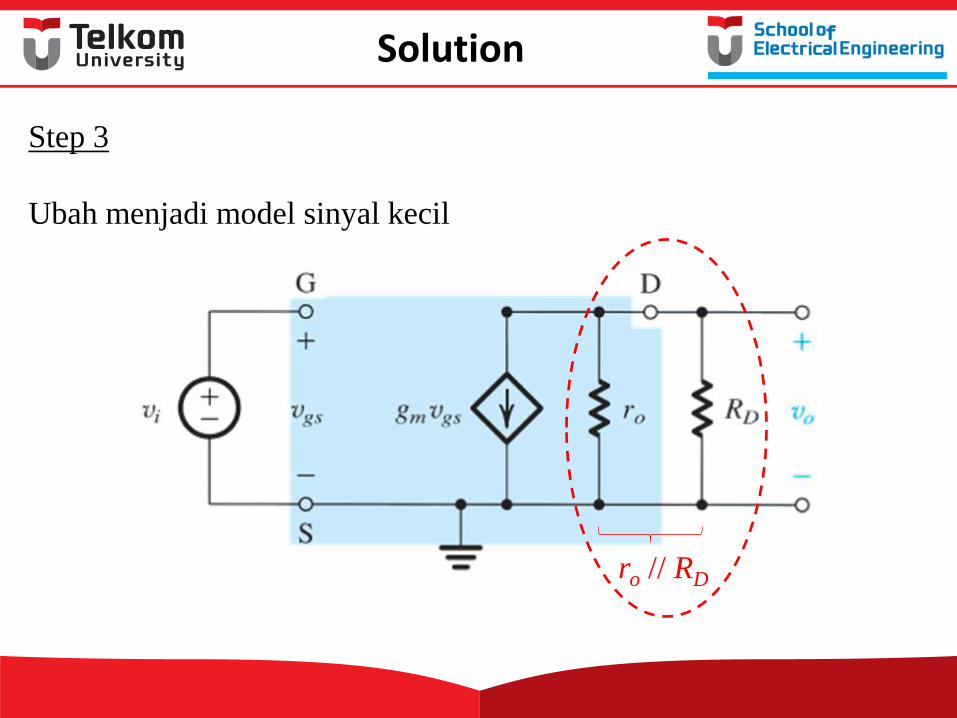
Step 3
Ubah menjadi model sinyal kecil
ro // RD
Solution
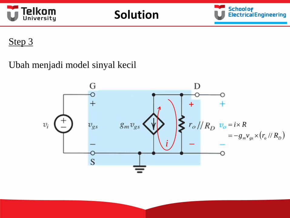
Step 3
Ubah menjadi model sinyal kecil
i Dogsm Rrvg
Ri
//
+
–
Solution